Embed Size (px)
Citation preview
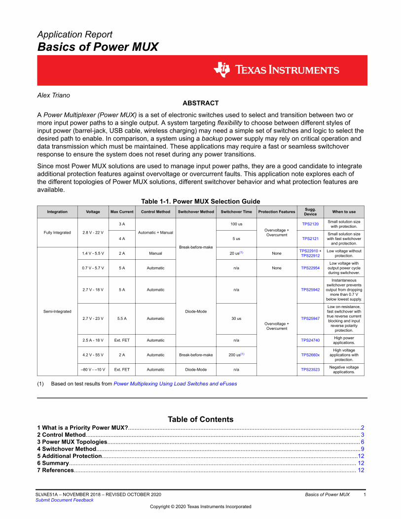
Application ReportBasics of Power MUX
Alex TrianoABSTRACT
A Power Multiplexer (Power MUX) is a set of electronic switches used to select and transition between two ormore input power paths to a single output. A system targeting flexibility to choose between different styles ofinput power (barrel-jack, USB cable, wireless charging) may need a simple set of switches and logic to select thedesired path to enable. In comparison, a system using a backup power supply may rely on critical operation anddata transmission which must be maintained. These applications may require a fast or seamless switchoverresponse to ensure the system does not reset during any power transitions.
Since most Power MUX solutions are used to manage input power paths, they are a good candidate to integrateadditional protection features against overvoltage or overcurrent faults. This application note explores each ofthe different topologies of Power MUX solutions, different switchover behavior and what protection features areavailable.
Table 1-1. Power MUX Selection GuideIntegration Voltage Max Current Control Method Switchover Method Switchover Time Protection Features Sugg.
Device When to use
Fully Integrated 2.8 V - 22 V
3 A
Automatic + Manual
Break-before-make
100 usOvervoltage +Overcurrent
TPS2120 Small solution sizewith protection.
4 A 5 us TPS2121Small solution sizewith fast switchover
and protection.
Semi-Integrated
1.4 V - 5.5 V 2 A Manual 20 us(1) None TPS22910 +TPS22912
Low voltage withoutprotection.
0.7 V - 5.7 V 5 A Automatic n/a None TPS22954Low voltage with
output power cycleduring switchover.
2.7 V - 18 V 5 A Automatic
Diode-Mode
n/a
Overvoltage +Overcurrent
TPS25942
Instantaneousswitchover preventsoutput from dropping
more than 0.7 Vbelow lowest supply.
2.7 V - 23 V 5.5 A Automatic 30 us TPS25947
Low on-resistance,fast switchover withtrue reverse currentblocking and input
reverse polarityprotection.
2.5 A - 18 V Ext. FET Automatic n/a TPS24740 High powerapplications.
4.2 V - 55 V 2 A Automatic Break-before-make 200 us(1) TPS2660xHigh voltage
applications withprotection.
–80 V - –10 V Ext. FET Automatic Diode-Mode n/a TPS23523 Negative voltageapplications.
(1) Based on test results from Power Multiplexing Using Load Switches and eFuses
Table of Contents1 What is a Priority Power MUX?..............................................................................................................................................22 Control Method....................................................................................................................................................................... 33 Power MUX Topologies.......................................................................................................................................................... 64 Switchover Method.................................................................................................................................................................95 Additional Protection............................................................................................................................................................126 Summary............................................................................................................................................................................... 127 References............................................................................................................................................................................ 12
www.ti.com Table of Contents
SLVAE51A – NOVEMBER 2018 – REVISED OCTOBER 2020Submit Document Feedback
Basics of Power MUX 1
Copyright © 2020 Texas Instruments Incorporated
8 Revision History................................................................................................................................................................... 12
List of FiguresFigure 1-1. Power MUX Block Diagram.......................................................................................................................................2Figure 1-2. Minimum Functionality for Power MUX Without Priority............................................................................................3Figure 1-3. Example Priority Power MUX.................................................................................................................................... 3Figure 2-1. Manual Power MUX using TPS22910 and TPS22912 Load Switches..................................................................... 4Figure 2-2. Automatic Power MUX using 2x TPS259470x eFuses............................................................................................. 5Figure 2-3. Automatic Power MUX with Manual Override using TPS2120..................................................................................6Figure 3-1. Manual and Automatic Discrete Power MUX with Priority.........................................................................................6Figure 3-2. Load Switch with Parasitic Body Diode Removed.....................................................................................................7Figure 3-3. Semi-Integrated Power MUX using TPS22910 and TPS22912 Load Switches........................................................7Figure 3-4. Semi-Integrated Power MUX using 2x TPS2660 eFuses......................................................................................... 8Figure 3-5. Fully-Integrated Priority Power MUX with TPS2120..................................................................................................9Figure 4-1. Voltage Dip on Output During Switchover Time...................................................................................................... 10Figure 4-2. Inrush Current Spike Caused by Supply Switchover...............................................................................................10Figure 4-3. Inrush Current Spike on IN2 During Switchover Using 2x TPS25942.....................................................................11
List of TablesTable 1-1. Power MUX Selection Guide...................................................................................................................................... 1
TrademarksAll other trademarks are the property of their respective owners.
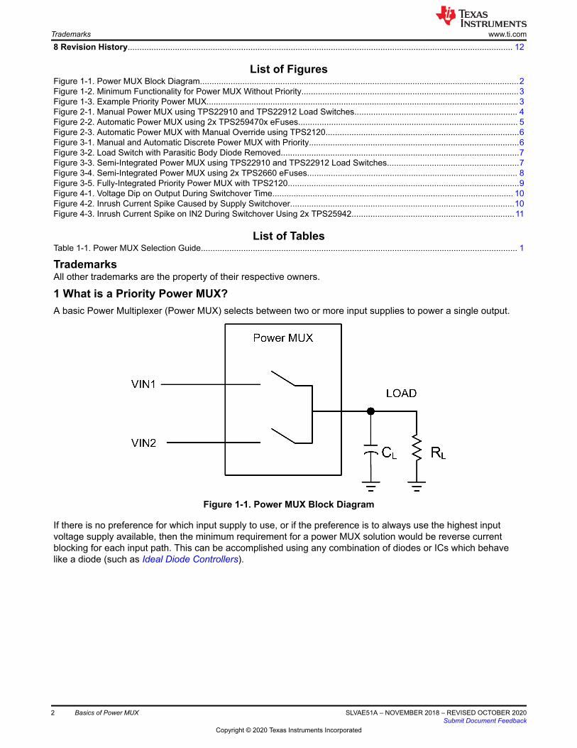
1 What is a Priority Power MUX?A basic Power Multiplexer (Power MUX) selects between two or more input supplies to power a single output.
Figure 1-1. Power MUX Block Diagram
If there is no preference for which input supply to use, or if the preference is to always use the highest inputvoltage supply available, then the minimum requirement for a power MUX solution would be reverse currentblocking for each input path. This can be accomplished using any combination of diodes or ICs which behavelike a diode (such as Ideal Diode Controllers).
Trademarks www.ti.com
2 Basics of Power MUX SLVAE51A – NOVEMBER 2018 – REVISED OCTOBER 2020Submit Document Feedback
Copyright © 2020 Texas Instruments Incorporated
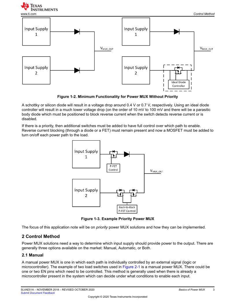
Figure 1-2. Minimum Functionality for Power MUX Without Priority
A schottky or silicon diode will result in a voltage drop around 0.4 V or 0.7 V, respectively. Using an ideal diodecontroller will result in a much lower voltage drop (on the order of 10 mV to 100 mV and there will be a parasiticbody diode which must be positioned to block reverse current when the switch detects reverse current or isdisabled.
If there is a priority, then additional switches must be added to have full control over which path to enable.Reverse current blocking (through a diode or a FET) must remain present and now a MOSFET must be added toturn on/off each power path to the load.
Figure 1-3. Example Priority Power MUX
The focus of this application note will be on priority power MUX solutions and how they can be implemented.
2 Control MethodPower MUX solutions need a way to determine which input supply should provide power to the output. There aregenerally three options available on the market: Manual, Automatic, or Both.
2.1 ManualA manual power MUX is one in which each path is individually controlled by an external signal (logic ormicrocontroller). The example of two load switches used in Figure 2-1 is a manual power MUX. There could beone or two EN pins which need to be controlled. This method is generally used when there is already amicrocontroller present in the system which can decide under what conditions to enable each input.
www.ti.com Control Method
SLVAE51A – NOVEMBER 2018 – REVISED OCTOBER 2020Submit Document Feedback
Basics of Power MUX 3
Copyright © 2020 Texas Instruments Incorporated
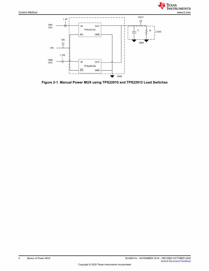
Figure 2-1. Manual Power MUX using TPS22910 and TPS22912 Load Switches
Control Method www.ti.com
4 Basics of Power MUX SLVAE51A – NOVEMBER 2018 – REVISED OCTOBER 2020Submit Document Feedback
Copyright © 2020 Texas Instruments Incorporated
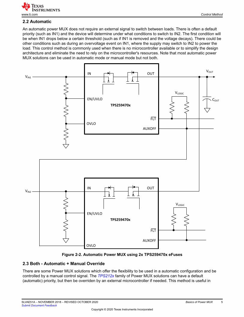
2.2 AutomaticAn automatic power MUX does not require an external signal to switch between loads. There is often a defaultpriority (such as IN1) and the device will determine under what conditions to switch to IN2. The first condition willbe when IN1 drops below a certain threshold (such as if IN1 is removed and the voltage decays). There could beother conditions such as during an overvoltage event on IN1, where the supply may switch to IN2 to power theload. This control method is commonly used when there is no microcontroller available or to simplify the designarchitecture and eliminate the need to rely on the microcontroller's resources. Note that most automatic powerMUX solutions can be used in automatic mode or manual mode but not both.
TPS259470x
IN OUT
EN/UVLO
VIN1
VOUT
COUT
OVLO
AUXOFF
VLOGIC
TPS259470x
IN OUT
EN/UVLO
VIN2
OVLO
AUXOFF
VLOGIC
FLT
FLT
Figure 2-2. Automatic Power MUX using 2x TPS259470x eFuses
2.3 Both - Automatic + Manual OverrideThere are some Power MUX solutions which offer the flexibility to be used in a automatic configuration and becontrolled by a manual control signal. The TPS212x family of Power MUX solutions can have a default(automatic) priority, but then be overriden by an external microcontroller if needed. This method is useful in
www.ti.com Control Method
SLVAE51A – NOVEMBER 2018 – REVISED OCTOBER 2020Submit Document Feedback
Basics of Power MUX 5
Copyright © 2020 Texas Instruments Incorporated
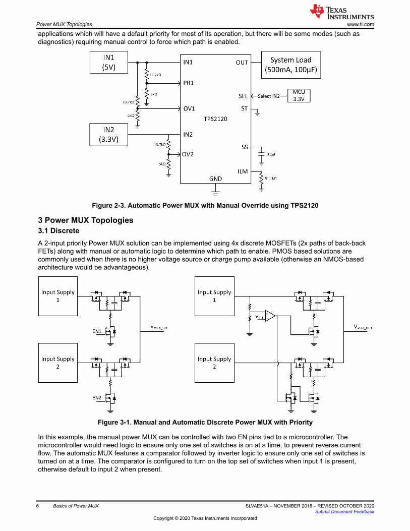
applications which will have a default priority for most of its operation, but there will be some modes (such asdiagnostics) requiring manual control to force which path is enabled.
Figure 2-3. Automatic Power MUX with Manual Override using TPS2120
3 Power MUX Topologies3.1 DiscreteA 2-input priority Power MUX solution can be implemented using 4x discrete MOSFETs (2x paths of back-backFETs) along with manual or automatic logic to determine which path to enable. PMOS based solutions arecommonly used when there is no higher voltage source or charge pump available (otherwise an NMOS-basedarchitecture would be advantageous).
Figure 3-1. Manual and Automatic Discrete Power MUX with Priority
In this example, the manual power MUX can be controlled with two EN pins tied to a microcontroller. Themicrocontroller would need logic to ensure only one set of switches is on at a time, to prevent reverse currentflow. The automatic MUX features a comparator followed by inverter logic to ensure only one set of switches isturned on at a time. The comparator is configured to turn on the top set of switches when input 1 is present,otherwise default to input 2 when present.
Power MUX Topologies www.ti.com
6 Basics of Power MUX SLVAE51A – NOVEMBER 2018 – REVISED OCTOBER 2020Submit Document Feedback
Copyright © 2020 Texas Instruments Incorporated
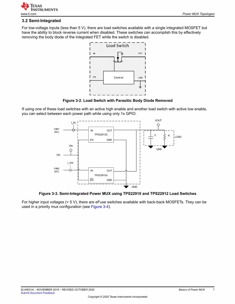
3.2 Semi-IntegratedFor low-voltage inputs (less than 5 V), there are load switches available with a single integrated MOSFET buthave the ability to block reverse current when disabled. These switches can accomplish this by effectivelyremoving the body diode of the integrated FET while the switch is disabled.
Figure 3-2. Load Switch with Parasitic Body Diode Removed
If using one of these load switches with an active high enable and another load switch with active low enable,you can select between each power path while using only 1x GPIO.
Figure 3-3. Semi-Integrated Power MUX using TPS22910 and TPS22912 Load Switches
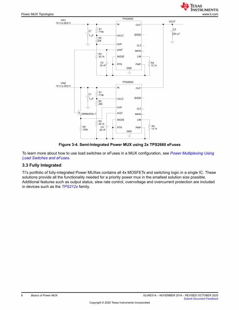
For higher input voltages (> 5 V), there are eFuse switches available with back-back MOSFETs. They can beused in a priority mux configuration (see Figure 3-4).
www.ti.com Power MUX Topologies
SLVAE51A – NOVEMBER 2018 – REVISED OCTOBER 2020Submit Document Feedback
Basics of Power MUX 7
Copyright © 2020 Texas Instruments Incorporated
IN OUT
UVLO
OVP
dVdT
RTN
LIM
IMON
GND
PWP
MODE
715k
20k
22 nF
R1
R2
C2
220 µF
C3
SHDN
FLT
12.1k
R4
VIN1
19 V to 28.8 V
TPS26600
IN OUT
UVLO
OVP
dVdT
RTN
LIM
IMON
GND
PWP
MODE
715k
20k
R1
R2
SHDN
FLT
12.1k
R4
TPS26600
1 µF
C1
VOUT
22 nF
C2
VIN2
19 V to 28.8 V
1 µF
C1
100k
R5
DMN62D0U-7
30.1k
R3
30.1k
R3
Figure 3-4. Semi-Integrated Power MUX using 2x TPS2660 eFuses
To learn more about how to use load switches or eFuses in a MUX configuration, see Power Multiplexing UsingLoad Switches and eFuses.
3.3 Fully IntegratedTI’s portfolio of fully-integrated Power MUXes contains all 4x MOSFETs and switching logic in a single IC. Thesesolutions provide all the functionality needed for a priority power mux in the smallest solution size possible.Additional features such as output status, slew rate control, overvoltage and overcurrent protection are includedin devices such as the TPS212x family.
Power MUX Topologies www.ti.com
8 Basics of Power MUX SLVAE51A – NOVEMBER 2018 – REVISED OCTOBER 2020Submit Document Feedback
Copyright © 2020 Texas Instruments Incorporated
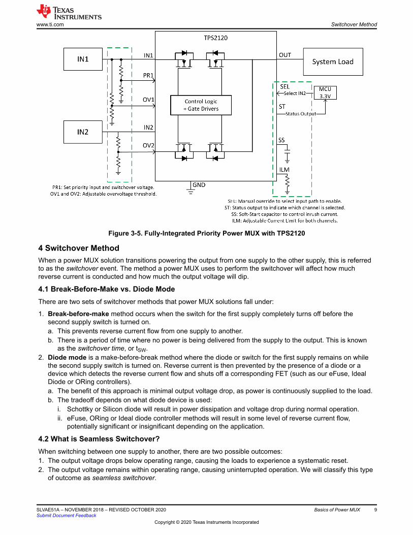
Figure 3-5. Fully-Integrated Priority Power MUX with TPS2120
4 Switchover MethodWhen a power MUX solution transitions powering the output from one supply to the other supply, this is referredto as the switchover event. The method a power MUX uses to perform the switchover will affect how muchreverse current is conducted and how much the output voltage will dip.
4.1 Break-Before-Make vs. Diode ModeThere are two sets of switchover methods that power MUX solutions fall under:
1. Break-before-make method occurs when the switch for the first supply completely turns off before thesecond supply switch is turned on.a. This prevents reverse current flow from one supply to another.b. There is a period of time where no power is being delivered from the supply to the output. This is known
as the switchover time, or tSW.2. Diode mode is a make-before-break method where the diode or switch for the first supply remains on while
the second supply switch is turned on. Reverse current is then prevented by the presence of a diode or adevice which detects the reverse current flow and shuts off a corresponding FET (such as our eFuse, IdealDiode or ORing controllers).a. The benefit of this approach is minimal output voltage drop, as power is continuously supplied to the load.b. The tradeoff depends on what diode device is used:
i. Schottky or Silicon diode will result in power dissipation and voltage drop during normal operation.ii. eFuse, ORing or Ideal diode controller methods will result in some level of reverse current flow,
potentially significant or insignificant depending on the application.
4.2 What is Seamless Switchover?When switching between one supply to another, there are two possible outcomes:1. The output voltage drops below operating range, causing the loads to experience a systematic reset.2. The output voltage remains within operating range, causing uninterrupted operation. We will classify this type
of outcome as seamless switchover.
www.ti.com Switchover Method
SLVAE51A – NOVEMBER 2018 – REVISED OCTOBER 2020Submit Document Feedback
Basics of Power MUX 9
Copyright © 2020 Texas Instruments Incorporated
If using a break-before-make power MUX, then switchover time is one key factor which will determine whether aseamless switchover will or will not occur. Faster switchover time will help achieve seamless switchover, at theexpense of higher inrush current. This balance should be considered and power MUX solutions are availablewith a range of switchover times.
If using a diode-mode or make-before-break power MUX, then seamless switchover is often possible sinceworst-case output voltage drop will be approximately 0.4 V to 0.7 V (depending on the diode used).
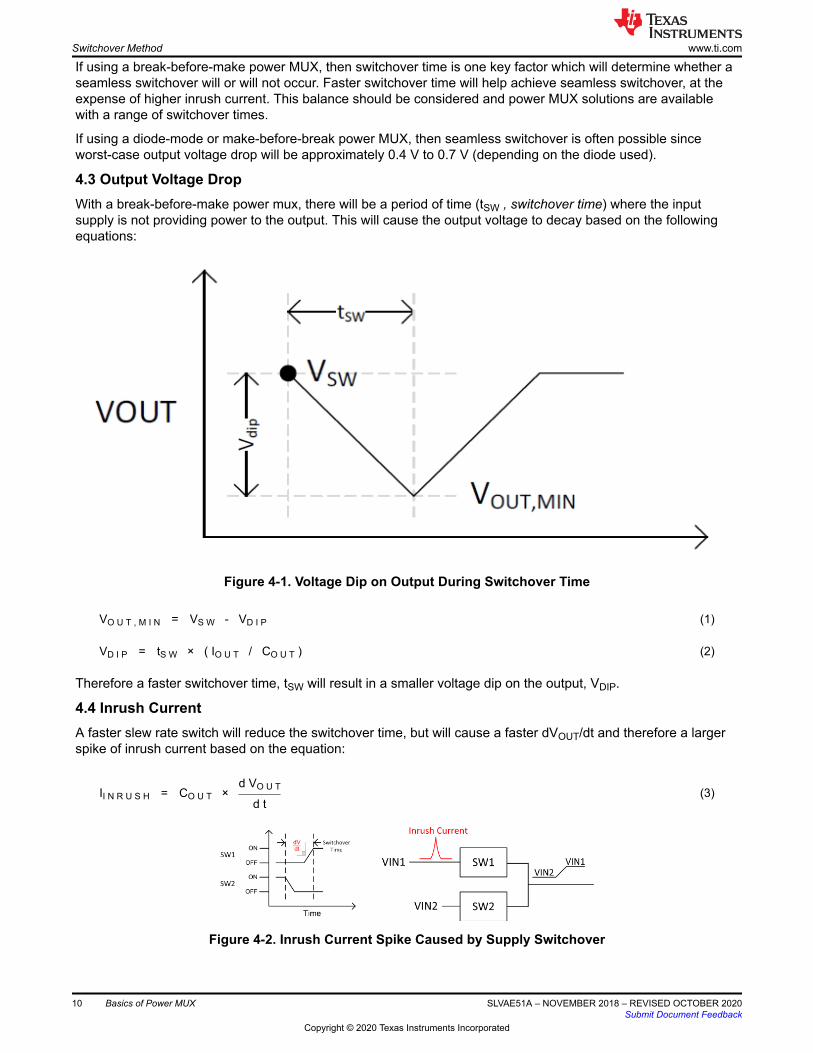
4.3 Output Voltage DropWith a break-before-make power mux, there will be a period of time (tSW , switchover time) where the inputsupply is not providing power to the output. This will cause the output voltage to decay based on the followingequations:
Figure 4-1. Voltage Dip on Output During Switchover Time
VO U T , M I N = VS W - VD I P (1)
VD I P = tS W × ( IO U T / CO U T ) (2)
Therefore a faster switchover time, tSW will result in a smaller voltage dip on the output, VDIP.
4.4 Inrush CurrentA faster slew rate switch will reduce the switchover time, but will cause a faster dVOUT/dt and therefore a largerspike of inrush current based on the equation:
II N R U S H = CO U T × d VO U T
d t(3)
Figure 4-2. Inrush Current Spike Caused by Supply Switchover
Switchover Method www.ti.com
10 Basics of Power MUX SLVAE51A – NOVEMBER 2018 – REVISED OCTOBER 2020Submit Document Feedback
Copyright © 2020 Texas Instruments Incorporated
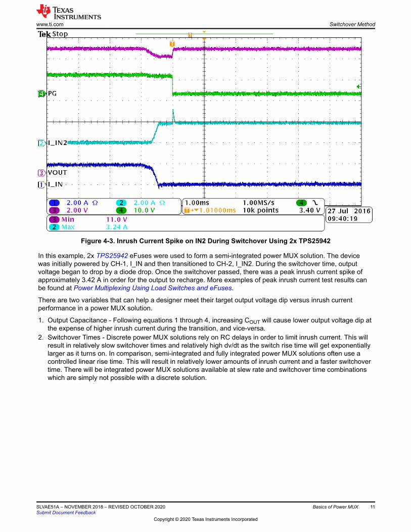
Figure 4-3. Inrush Current Spike on IN2 During Switchover Using 2x TPS25942
In this example, 2x TPS25942 eFuses were used to form a semi-integrated power MUX solution. The devicewas initially powered by CH-1, I_IN and then transitioned to CH-2, I_IN2. During the switchover time, outputvoltage began to drop by a diode drop. Once the switchover passed, there was a peak inrush current spike ofapproximately 3.42 A in order for the output to recharge. More examples of peak inrush current test results canbe found at Power Multiplexing Using Load Switches and eFuses.
There are two variables that can help a designer meet their target output voltage dip versus inrush currentperformance in a power MUX solution.
1. Output Capacitance - Following equations 1 through 4, increasing COUT will cause lower output voltage dip atthe expense of higher inrush current during the transition, and vice-versa.
2. Switchover Times - Discrete power MUX solutions rely on RC delays in order to limit inrush current. This willresult in relatively slow switchover times and relatively high dv/dt as the switch rise time will get exponentiallylarger as it turns on. In comparison, semi-integrated and fully integrated power MUX solutions often use acontrolled linear rise time. This will result in relatively lower amounts of inrush current and a faster switchovertime. There will be integrated power MUX solutions available at slew rate and switchover time combinationswhich are simply not possible with a discrete solution.
www.ti.com Switchover Method
SLVAE51A – NOVEMBER 2018 – REVISED OCTOBER 2020Submit Document Feedback
Basics of Power MUX 11
Copyright © 2020 Texas Instruments Incorporated
5 Additional ProtectionSince power MUX solutions are often used at the input to a system, it is a good location to integrate protectionfeatures such as overvoltage or overcurrent protection.
5.1 Overvoltage ProtectionSome applications need to protect against undesired high-voltage DC supplies or against transient inducedvoltages (such as from surge events or inductive switching). These potentially harmful voltages can be blockedfrom downstream components by using a power MUX with protection.
5.2 Overcurrent ProtectionIf a downstream circuit or fault event begins to draw excessive amounts of current, it is essential to limit thatcurrent quickly to avoid potential circuit damage or fire. This is another level of protection that can be integratedwithin a power mux.
TI provides power mux solutions with both overvoltage and overcurrent protection. For example, 2x TPS2660 or2x TPS25947 are semi-integrated power MUX solutions and TPS212x is a fully-integrated power MUX whicheach offer this level of protection.
6 SummaryThere are different power MUX control methods, topologies, and switchover methods which offer a certain levelof flexibility, protection and performance. System concerns such as output voltage drop or inrush current can beaddressed by utilizing Texas Instruments' portfolio of semi-integrated Load Switch and eFuse solutions, or afully-integrated Power MUX such as the TPS212x family which can offer the highest level of functionality in thesmallest size available.
7 References• Seamless Switchover for Backup Power Reference Design• Power Multiplexing Using Load Switches and eFuses• Basics of eFuses
8 Revision HistoryNOTE: Page numbers for previous revisions may differ from page numbers in the current version.
Changes from Revision * (November 2018) to Revision A (October 2020) Page• Updated the numbering format for tables, figures and cross-references throughout the document...................2
Additional Protection www.ti.com
12 Basics of Power MUX SLVAE51A – NOVEMBER 2018 – REVISED OCTOBER 2020Submit Document Feedback
Copyright © 2020 Texas Instruments Incorporated

IMPORTANT NOTICE AND DISCLAIMER
TI PROVIDES TECHNICAL AND RELIABILITY DATA (INCLUDING DATASHEETS), DESIGN RESOURCES (INCLUDING REFERENCE DESIGNS), APPLICATION OR OTHER DESIGN ADVICE, WEB TOOLS, SAFETY INFORMATION, AND OTHER RESOURCES “AS IS” AND WITH ALL FAULTS, AND DISCLAIMS ALL WARRANTIES, EXPRESS AND IMPLIED, INCLUDING WITHOUT LIMITATION ANY IMPLIED WARRANTIES OF MERCHANTABILITY, FITNESS FOR A PARTICULAR PURPOSE OR NON-INFRINGEMENT OF THIRD PARTY INTELLECTUAL PROPERTY RIGHTS.These resources are intended for skilled developers designing with TI products. You are solely responsible for (1) selecting the appropriate TI products for your application, (2) designing, validating and testing your application, and (3) ensuring your application meets applicable standards, and any other safety, security, or other requirements. These resources are subject to change without notice. TI grants you permission to use these resources only for development of an application that uses the TI products described in the resource. Other reproduction and display of these resources is prohibited. No license is granted to any other TI intellectual property right or to any third party intellectual property right. TI disclaims responsibility for, and you will fully indemnify TI and its representatives against, any claims, damages, costs, losses, and liabilities arising out of your use of these resources.TI’s products are provided subject to TI’s Terms of Sale (www.ti.com/legal/termsofsale.html) or other applicable terms available either on ti.com or provided in conjunction with such TI products. TI’s provision of these resources does not expand or otherwise alter TI’s applicable warranties or warranty disclaimers for TI products.
Mailing Address: Texas Instruments, Post Office Box 655303, Dallas, Texas 75265Copyright © 2020, Texas Instruments Incorporated