Embed Size (px)
Citation preview
This document is downloaded from DR‑NTU (https://dr.ntu.edu.sg)Nanyang Technological University, Singapore.
Beamsteering antennas using liquid crystals for5G applications
Divya Krishnan
2020
Divya Krishnan. (2020). Beamsteering antennas using liquid crystals for 5G applications.Master's thesis, Nanyang Technological University, Singapore.
https://hdl.handle.net/10356/144902
https://doi.org/10.32657/10356/144902
This work is licensed under a Creative Commons Attribution‑NonCommercial 4.0International License (CC BY‑NC 4.0).
Downloaded on 29 Jan 2022 00:53:09 SGT
i
BEAMSTEERING ANTENNAS USING LIQUID CRYSTALS
FOR 5G APPLICATIONS
DIVYA KRISHNAN
School of Electrical & Electronic Engineering
A thesis submitted to the Nanyang Technological University
in partial fulfillment of the requirement for the degree of
Master of Engineering
2020
ii
STATEMENT OF ORIGINALITY
I hereby certify that the work embodied in this thesis is the result of original
research, is free of plagiarised materials, and has not been submitted for a higher
degree to any other University or Institution.
[Provide Student’s Signature Here]
.. 22/11/2020. . . . . . . . . Divya Krishnan. . . . . . . .
Date [Key in Student’s Name Here]
iii
SUPERVISOR DECLARATION STATEMENT
I have reviewed the content and presentation style of this thesis and declare it is
free of plagiarism and of sufficient grammatical clarity to be examined. To the
best of my knowledge, the research and writing are those of the candidate except
as acknowledged in the Author Attribution Statement. I confirm that the
investigations were conducted in accord with the ethics policies and integrity
standards of Nanyang Technological University and that the research data are
presented honestly and without prejudice.
[Enter Date in dd-mm-yy] [Provide Supervisor’s Signature Here]
. 22/11/2020. . . . . . .. ……... . Alphones Arokiaswami. . . . . . . .
Date [Key in Supervisor’s Name Here]

iv
AUTHORSHIP ATTRIBUTION STATEMENT
This thesis contains material from 2 paper(s) published in the following peer-
reviewed journal(s) / from papers accepted at conferences in which I am listed as an
author.
Chapter 4 is published in Asia Pacific Microwave Conference (APMC), Singapore,
2018 conference paper titled ‘Enhanced Frequency Tuning based on Optimized
Liquid Crystal Cavity Patch Antenna’ and accepted for presentation in Antenna and
Propogation Society (AP-S), Montreal, Canada, 2020 conference paper titled ‘Liquid
Crystal Material based Electronically Beam Steering Antenna at Ka-band for 5G
Applications’.
The contributions of the co-authors are as follows:
• Mr Alphones supervised and provided valuable feedback and editing of the
final draft
• Mr. Nasimuddin helped conduct simulation studies required to add in the
paper and provided the technology and material details and also helped in
editing of paper
• I wrote the paper and ran the simulations to see its working and included in
the paper
[Enter Date in dd-mm-yy] [Provide Student’s Signature Here]
. . 22/11/2020. . . . .Divya Krishnan . . . . . .
Date [Key in Student’s Name Here]
v
ACKNOWLEDGEMENT
I would like to extend my sincere gratitude to everyone who helped in making
me complete this work successfully. I thank my supervisor Prof Alphones
Arokiaswami wholeheartedly for his continued support in every stage of my
candidature including project design, conceptualization and editing. I am
forever grateful for the advice and feedback that proved to be very valuable
in this journey.
Next, I thank Dr. Nasimuddin of I2R Department, A*STAR for his sincere
and innovative ideas and unwavering support that led to the completion of
this work as well as for access to the labs and technology at A*STAR that
made this project possible.
I further note my eternal gratitude to my family and close friends who
provided me with the motivation and love that enabled me to do this work
completely.
vi
Table of Contents
STATEMENT OF ORIGINALITY .................................................................................... ii
SUPERVISOR DECLARATION STATEMENT ............................................................. iii
AUTHORSHIP ATTRIBUTION STATEMENT ............................................................. iv
ACKNOWLEDGEMENT ................................................................................................... v
ABBREVIATIONS .............................................................................................................. x
SUMMARY ....................................................................................................................... xiii
LIST OF FIGURES ........................................................................................................... xv
LIST OF TABLES ............................................................................................................ xix
Chapter 1 INTRODUCTION ............................................................................................. 1
1.1. General Background .............................................................................................. 1
1.2. Motivation for the Project ...................................................................................... 3
1.3. Organisation of Thesis ........................................................................................... 3
Chapter 2 LITERATURE REVIEW ................................................................................. 5
2.1. 5G - An Overview of Technology ......................................................................... 5
2.1.1. The Need For 5G .................................................................................. 5
2.1.2. 5G Spectra and Standards ..................................................................... 7
2.2. Massive MIMO Technology .................................................................................. 9
2.2.1. mm-Wave with Massive MIMO ......................................................... 10
2.3. Beamforming and Beamsteering .......................................................................... 12
2.3.1. Beamforming - definition and principle ............................................. 12

vii
2.3.2. Beamsteering and Beam Switching .................................................... 13
2.3.3. Beamforming techniques .................................................................... 13
2.3.4. Beamsteering techniques .................................................................... 14
2.3.4. Conclusions ......................................................................................... 18
2.4. Liquid Crystals ..................................................................................................... 19
2.4.1. Physical Properties and Behaviour .......................................................... 19
2.4.2. Reaction to external Electric Field ...................................................... 21
2.4.3. LC Based Beamteering techniques ..................................................... 23
Chapter 3 MEANDERLINE FEED AND INTERDIGITATED FEED COMPARISON
WITH LC LAYER ............................................................................................................. 26
3.1. Introduction .......................................................................................................... 26
3.2. Meanderline feed .................................................................................................. 26
3.3. Interdigitated feed ................................................................................................ 30
3.4. Conclusion ........................................................................................................... 35
Chapter 4 PATCH ANTENNA WITH LC AND MEANDERLINE - LC CAVITY
DESIGN AND BEAMSCANNING .................................................................................. 36
4.1. Introduction .......................................................................................................... 36
4.1. Cavity design using Liquid Crystal ...................................................................... 38
4.1.1. Results ................................................................................................. 43
4.2. The Meanderline Feed with Patch Antenna and LC Layer .................................. 43
4.2.1. 1 x 4 Array .......................................................................................... 44
viii
4.2.2. Results ................................................................................................. 46
4.2.3. 4 X 4 Array ......................................................................................... 48
4.2.4. Results ................................................................................................. 48
4.3. Flipped Structure .................................................................................................. 50
4.3.1. 1 X 4 flipped array .............................................................................. 51
4.3.2. Results ................................................................................................. 52
4.3.3. 4 x 4 flipped array ............................................................................... 53
4.3.4. Results ................................................................................................. 54
4.4. Conclusion ........................................................................................................... 56
Chapter 5 LEAKY WAVE ANTENNAS WITH LC ...................................................... 58
5.1. Introduction .......................................................................................................... 58
5.2. Design of circular LWA ....................................................................................... 64
5.2.1. Results ................................................................................................. 67
5.3. Design of Square LWA ........................................................................................ 69
5.3.1. Results ................................................................................................. 70
5.4. Conclusion ........................................................................................................... 72
Chapter 6 STAR SHAPED LWA AND TWA WITH LC .............................................. 73
6.1. Introduction .......................................................................................................... 73
6.2. Design of Star shaped TWA ................................................................................ 74
6.2.1. Results ................................................................................................. 77
6.3. Design of Star shaped LWA ................................................................................ 77
ix
6.3.1. Results ................................................................................................. 79
6.4. Star shaped array .................................................................................................. 81
6.4.1. Results ................................................................................................. 83
6.4.2. Fabricated Structure ............................................................................ 88
6.4.3. Results ..................................................................................................... 90
6.5. Conclusions .......................................................................................................... 91
Chapter 7 CONCLUSIONS AND FUTURE WORK ..................................................... 92
AUTHOR’S PUBLICATIONS ......................................................................................... 98
BIBLIOGRAPHY .............................................................................................................. 99
x
ABBREVIATIONS
5G …………………………………………………………………………… 5th Generation
MIMO ………………………………………………………. Massive Input Massive Output
RF-MEMS ………………………….. Radio Frequency Micro Electro Mechanical System
LC…..………………………………………………………………………… Liquid Crystal
DC…………………………….………………………………………………. Direct Current
OFDM ....……………………………………. Orthogonal Frequency Division Multiplexing
LTE ………………………………………….……………………….. Long Term Evolution
3D ……………………………………….…………………………………… 3 Dimensional
LWA ..………………………………………………………………… Leaky Wave Antenna
TWA .…………………………………………………………..… Travelling Wave Antenna
HetNets …………………………………………………………… Heterogeneous Networks
Gbps ...……………………………………………..…………………… Giga bits per second
UHD ….……………………………………………..………………… Ultra High Definition
AR …………………………………………………….………………… Augmented Reality
VR ...……………………………………………………….………………… Virtual Reality
IoT …………………………………….…………………..……………… Internet of Things
NR …..……………………………..…………………………..………………… New Radio
TDD ...…………………………………..………………………… Time Division Duplexing
GDPA …………………………………..………………………….. Gross Domestic Product
3GPP ….…………………………………….…………… 3rd Generation Partnership Project
ITU ……...………………………………………… International Telecommunication Union
WRC ……………………………………………………………… World Radio Convention
EB ……………..…………………………………………………… Elevation Beamforming
Rel ..………………………………………………………….……………………… Release
BS …………………………………………………….………………………… Base Station
SNR …………………………………………………………………… Signal to Noise Ratio
FDD …………………………………………………………… Full Dimensional Duplexing
PIN ……………………………………………………………… Positive-Intrinsic-Negative
MEMS ….…………………………………..…………… Micro-electro-Mechanical System
xi
FET ..……………………………………………….………………… Field Effect Transistor
ADC ………………………………………………………… Alternating and Direct Current
TXRU …..………………………………………….…………… Transmission Receive Unit
ESPAR …...…………………………….… Electronically Steerable Parasitic Array Radiator
CSPA …………..…………………………..…………… Circular Switched Parasitic Array
RH …..…………………………………..…………….………………………… Right Hand
LH …..…………………………………….…………….………………………… Left Hand
CRLH ...………………………………………………………… Composite Right Left Hand
PLTWA ...………………………….……………… Patch Loaded Travelling Wave Antenna
dB ...………………………………………………………………………………… Decibels
FSS …………………….……………………………………… Frequency Selective Surface
NLC ….……………………….……….…………………………… Nematic Liquid Crystal
5CB ….……………………………….………………….……… 4-cyano-4’-pentylbiphenyl
SIW …………………………..……….…………………… Substrate Integrated Waveguide
DRA ……………………………………………….………… Dielectric Resonator Antenna
GAA ………………………………………….………………………… Grid Array Antenna
MHz …...…………………………………….…….…….……………………… Mega Hertz
GHz …..……………………………………………..…………………………… Giga Hertz
xii
SYMBOLS
α ………………………….…………………………………………..…………. Attenuation
λ ………………………………………………………..……….…….………… Wavelength
β …………………………………………….……….……....….…………… Phase Constant
θ …………………………………………….……….………….………..…………… Angle
k ……………………………………………….……………………… Propagation Constant
δ .…………………………….…………………………………….………….. Dielectric loss
ε …………………………..…………………………….…………..…………… Permittivity
L .…………………………………………………………. Length of microstrip antenna feed
d …..…………………………………..……. Separation Distance between antenna elements
W/ Wf …….……………………………………..……………………………… Patch width
h ….………………………………………………………...……………….. Substrate height
t ..……………………………..…………………………..……………………….. Thickness
xiii
SUMMARY
5G being a buzzword in telecommunication has led to the invention of many novel
designs of antennas that cater to the 5G protocols, techniques and applications.
Antenna arrays with small form factor, able to show ability of mainlobe scanning thus
became a necessity to be able to implement Massive Input Massive Output (MIMO)
arrays as part of the 5th Generation applications.
Liquid Crystals (LC’s) were a class of materials gaining traction in beamscanning
applications due to the ability of integration of these materials in planar and compact
surfaces. Their unique properties regarding permittivity change with applied voltage
thus could be harnessed in various ways. This opened up a new era of antenna
configurations and feed networks that solely worked on integration with LC
materials.
The focus of this thesis is thus on different types of planar antenna array systems used
in telecommunication and their behavior and advantage when integrated with an LC
layer.
Starting with an Introduction and Literature Review in which various 5G terms,
protocol and definitions, the existing methods of beamscanning technologies and the
drawbacks of each as well as need for a more easy-to-integrate beamscanning
technique is discussed, the properties of Liquid Crystals that make it suitable for the
same is also described in detail.
Next, various types of beamscanning configurations are investigated starting with the
basic rectangular patch antennas. The patch antenna array system is the most common
type of array used in 5G beamforming and MIMO applications due to the relative
ease of design and compact structure as well as low cost of fabrication. On integrating
with the LC layer, it can be seen to show a larger scanning range with relatively less
modifications in array geometry and working principles. In addition to being applied
underneath the patch itself, LC layer can also be used in the feed network of a patch
array and can be used to provide variable phase shifts as in a delay line topology. A
xiv
simple and effective feed system with LC layer is proposed that can be integrated to
provide required phase shift for any antenna configuration.
Later, Leaky Wave Antennas and Travelling Wave Antennas and their reaction to the
LC layer in the network is studied. A novel shape of LWA design and its advantages
are also defined. The LWA’s provide multiple degrees of freedom in beamscanning
due to the property of the array to act as a variable delay line with differential phase
shift. This is combined with the LC permittivity change property to provide greater
angles of scanning. The LWA design has been found to overcome various drawbacks
of the initial designs including ease of practical application of a DC bias to the LC
layer as well as stable gain during resonant frequency change with permittivity
change of LC layer. Lower sidelobes for the beam is observed.
The designs mentioned have been modified and tuned to satisfy 5G protocol
requirements like resonant frequency range, gain cutoffs and scanning angle
requirements.
Depending on the problem statement, we can thus use a different type of antenna
array along with the embedded LC layer. Each type has its own advantages and
drawbacks, but many limitations of the scanning range is overcome using a very
simple method of adding a variable permittivity Liquid Crystal layer.
This work is thus an investigation in how different antenna arrays work to enable and
support beamscanning as well as the requirements, standards and technologies that
make 5G MIMO beamscanning a reality. It also describes how the use of a simple
metamaterial modification can be applied to any type of array and how each response
is unique.
The conclusion gives an overview of the problems incurred at each level of antenna
design and how to overcome the challenges as well as the future of LC’s in
beamscanning.
xv
LIST OF FIGURES
Figure 2-1. The PLTWA of [26] .............................................................................. 16
Figure 2-2. The CRLH antenna of [27] and equivalent circuit ................................ 17
Figure 2-3. Temperature dependant phases of calamitic LCs [33] .......................... 20
Figure 2-4. Anchoring and behavior of LC with applied DC voltage [35] .............. 22
Figure 3-1. Impedence equivalent of a meanderline’s shorter sides [41] ................ 27
Figure 3-2. Meanderline feed design with 0.503mm RO4350B substrate layer and
0.25mm LC layer with optimized length of line 4.4 mm, with 0.25 mm and thickness
0.1 mm. .................................................................................................................... 28
Figure 3-3. Phase shift caused for different values of permittivity of LC layer ...... 29
Figure 3-4. Magnitude of S-parameters(S11) for changing permittivity of LC layer 29
Figure 3-5. Interdigitated finger design on Rogers RO4530B substrate of 0.503 mm
thickness and embedded LC layer of 0.25 mm with optimized length of fingers 3.5
mm, side length 4.2 mm and thickness 0.2 mm. ...................................................... 31
Figure 3-6. S21_Phase values vs frequency using interdigitated structure for 0.25 mm
LC layer under 0.503 mm RO4350B substrate with LC permittivities 2.5, 3 and 3.5
respectively- a) through the large frequency band b) for required range(28-30 GHz).
.................................................................................................................................. 32
Figure 3-7. Comparison of phase shifts between meanderline and interdigitated feed
with varying LC permittivity (2.5, 3 and 3.5) …………………………………….. 33
Figure 3-8. Comparison of phase shifts caused by different types of LC beamsteering
techniques……………………..…………………………………………………... 34
Figure 4-1. Patch antenna with a dielectric layer and ground plane [43] ................ 36
Figure 4-2. Radiation diagram of patch antenna [45] .............................................. 37
Figure 4-3. Cavity design for LC layer of 0.25 mm in a 1 mm ground layer with a
substrate layer, RO4530B of 0.25 mm on top and patch antenna printed above it. 39
Figure 4-4. Cavity shapes and dimensions .............................................................. 40
Figure 4-5. Frequency change for rectangular cavity .............................................. 41
Figure 4-6. Frequency change for Pillar-shape cavity ............................................. 41
Figure 4-7. Frequency change for I-shape cavity .................................................... 42
Figure 4-8. 1X4 array design with embedded LC layer in ground layer, both 0.25 mm
and a thicker substrate layer of 0.803 mm thickness on top. The meanderline is printed
xvi
on the embedded LC layer and connected to patch antenna and impedence matching
network on top using vias. ....................................................................................... 45
Figure 4-9. 1X4 patch antenna array ........................................................................ 45
Figure 4-10. Radiation pattern shift for the configuration by keeping all LC layers of
same permittivity and by keeping them successively 2.5, 2.8, 3.2 and 3.5, to induce
phase shift in the array. ............................................................................................ 46
Figure 4-11. 3D radiation pattern with a) all LC layers same permittivity and b) LC
layers having 2.5, 2.8, 3.2 and 3.5 permittivities. .................................................... 47
Figure 4-12. 4x4 patch array .................................................................................... 48
Figure 4-13. Radiation pattern shift for the configuration by keeping all LC layers of
same permittivity and by keeping them successively 2.5, 2.8, 3.2 and 3.5, to induce
phase shift in the array. ............................................................................................ 49
Figure 4-14. 3D view of radiation pattern with all LC layers same permittivity(3). 49
Figure 4-15. Flipped design by connecting meanderline feed on the bottom side of
embedded LC layer (0.25 mm) in ground plane (1 mm) and patch antenna on the
opposite side above another substrate layer(0.25 mm), through vias. Impedence
matching network on bottom side below another substrate layer. ........................... 50
Figure 4-16. Front view of flipped patch array ........................................................ 51
Figure 4-17. Back view of flipped patch array ........................................................ 52
Figure 4-18. Farfield result with phase shift by comparing all LC layers of same
permittivity and for successively 2.5, 2.8, 3.2 and 3.5 of the array. ........................ 52
Figure 4-19. 3D farfield beam with phase shift seen due to LC layers having different
permittivities. ........................................................................................................... 53
Figure 4-20. Top and back view of design .............................................................. 54
Figure 4-21. Farfield result ...................................................................................... 55
Figure 4-22. 3D farfield beam showing higher directivity with this configuration, for
all LC layers same permittivity(3). .......................................................................... 56
Figure 5-1. Radiation patterns of electric fields in a) Parallel plate waveguide b)
coaxial line c) stripline d) microstrip[47] ................................................................ 58
Figure 5-2. Current and field radiation patterns of a slot in a waveguide [47] ........ 59
Figure 5-3. Conventional LWA [47] ....................................................................... 60
Figure 5-4. Transmission coefficient behavior as a function of propagation constants
for conventional LWA [49] ..................................................................................... 63
Figure 5-5. Dependence of transmission wavelength to slit width in a LWA [47] . 63
xvii
Figure 5-6. Transmission coefficient vs propagation constant enhancement using
design techniques [49] ............................................................................................. 64
Figure 5-8. LWA design with LC layer of 0.5 mm inside a sybstrate layer of 0.762mm
thickness, with LWA on the embedded LC layer connected to feed network on top
using vias. ................................................................................................................ 65
Figure 5-9. Top view of circular LWA structure ..................................................... 66
Figure 5-10. Dimensions of design .......................................................................... 66
Figure 5-11. S11 of the circular LWA design ........................................................... 67
Figure 5-12. Gain vs frequency ............................................................................... 68
Figure 5-13. Farfield phase shift by using LC layer of permittivity 2.5 vs 3.5. ...... 68
Figure 5-14. Top view of structure .......................................................................... 69
Figure 5-15. Dimensions of square LWA ................................................................ 70
Figure 5-16. S11 of the square LWA design ............................................................. 70
Figure 5-17. Gain vs frequency ............................................................................... 71
Figure 5-18. Farfield phase shift using LC layer of permittivity 2.5 vs 3.5. ........... 71
Figure 6-1. Types of TWA designs from top left : the comb MTWA, Meanderline
type MTWA, Rectangular loop type MTWA, Franklin type MTWA, Normal TEM
line terminated in matched resistive load [52] ......................................................... 73
Figure 6-2. Circuit equivalent of the matched resistive termination TWA with
radiation pattern[52] ................................................................................................. 74
Figure 6-3. Normal patch loaded TWA structure design with star shaped patch slots
in feedline with embedded LC Layer inside Rogers substrate(RO4350B). ............. 75
Figure 6-4. Top view of star patch TWA ................................................................. 75
Figure 6-5. Dimensions of star patch ....................................................................... 76
Figure 6-6. Radiation pattern shift by changing permittivity of LC from 2.5 to 3.5.
.................................................................................................................................. 77
Figure 6-7. Top view of designed LWA by using only star shaped slot radiators on
0.5 mm LC layer and no patch loading. The slot radiators are underneath a 0.762 mm
Rogers RO4530B layer and connected to feed network through vias on both sides.
.................................................................................................................................. 78
Figure 6-8.Dimensions of design ............................................................................. 78
Figure 6-9. S11 values of the antenna at 3 different permittivities of LC ................. 79
Figure 6-10. Farfield pattern shift with changing LC permittivity from 2.5, 3 and 3.5.
.................................................................................................................................. 80
xviii
Figure 6-11. Gain vs frequency ............................................................................... 80
Figure 6-12. Top view of star LWA array ............................................................... 81
Figure 6-13. Dimensions of star shaped LWA design with LC layers having different
permittivities. ........................................................................................................... 83
Figure 6-14. S11 values of the LWA array for different values of permittivity of LC
.................................................................................................................................. 84
Figure 6-15. Farfield pattern for different LC permittivitie, 2.5, 3 and 3.5. ............ 85
Figure 6-16. Farfield patterns for 3 groups of phases applied at feeds. ................... 86
Figure 6-17. Gain vs frequency ............................................................................... 86
Figure 6-18. Beam scanning as a function of frequency for the array ..................... 87
Figure 6-19. Beamshift due to same(all 3) and different permittivities(2.5, 2.8, 3.2
and 3.5) applied to adjacent rows of antenna array. ................................................ 88
Figure 6-20. Top view of star-LWA array ............................................................... 89
Figure 6-21. LC cavity ............................................................................................. 89
Figure 6-22. S11 comparison of experimental vs simulated ..................................... 90
Figure 7-1. Top view of Grid Array Antenna .......................................................... 95
Figure 7-2. Grid antenna designed ........................................................................... 95
Figure 7-3. Beamscanning due to LC permittivity change ...................................... 96
Figure 7-4. S11 resonance change with permittivity ................................................. 96
xix
LIST OF TABLES
Table 1. 5G frequency bands and functions ……………………………….... 28
Table 2. Beamforming Techniques and their features ……………………… 44
Table 3. Frequency shift comparison for 2 types of feed …………………… 61
Table 4. Comparison of LC based phase shifters ………………………….... 61
Table 5. Cavity Tuning range ………………………………………………...70
1
CHAPTER 1 INTRODUCTION
1.1. General Background
The most pivotal technological advance in the 21st century in communications
domain has been the introduction of 5G or 5th Generation cellular network
technology. Mobile communication had become an inevitable part of daily life by the
late 20th century and ever since its advance, demands have increased for higher data
rates, faster networks and more user-friendly applications. 4G LTE (Long Term
Evolution) was an important advancement that gave consumers an idea of how a
frequency spectrum could be harnessed in previously unidentified ways to provide
significantly faster speed as well as advanced applications like video conferencing,
mobile TV etc. This led to an interest in how this technology could be further
developed to create drastically higher performance and better user interfaces. As a
result, companies like Huawei, Xilinx and Qualcomm started trials and testing of 5G
products in allotted bands in various countries by the end of 2010. [1]
Some key innovative ideas/technologies facilitate the introduction of such a high
efficiency, high capacity communication link, the most important being: massive
MIMO (Multi-input, Multi-Output) arrays, Beamforming and Millimeter-wave
antennas/circuits. Massive MIMO implies using a very large number of antennas for
transmission of signal bits simultaneously and being received by the end system, so
that net transfer rate or bit rate is high. The number of antennas could be as large as
256 or 1280 in an array, which requires that they be of small form factor and low cost
in order to deploy to the masses.
Another key term used is Beamforming, which refers to creating a main beam in an
antenna array and using phase shifters and other methods to steer the beam to desired
direction.
Millimeter arrays refer to tiny antennas that can transmit at very high frequencies, to
the order of GigaHertz frequencies.
2
Massive MIMO systems require small antennas with high directivity that can employ
beamforming and beamsteering for them to communicate with each other efficiently.
As a part of the research to find a new and efficient method of beamsteering, various
methods were investigated. RF-MEMS (Radio Frequency- Micro-Electro-
Mechanical System), Reflectarrays, Mechanical actuators etc. were all used
conventionally for beamsteering purposes. Scientists later developed various
metamaterials that could effectively combine with an antenna array to direct the beam
formed in a desired direction. A metamaterial structure in relation to an antenna array
usually consists of a changeable electrical length feed designed to provide variable
phase shift to the elements of an antenna array.
Liquid Crystals were one such material that gained interest during this time since
their variable permittivity posed an intriguing electrical property that could be
combined with an antenna array. They had the advantage of being largely invariable
to temperature and interference effects, as well as being easy to integrate on planar
surfaces like a smartphone. The material losses incurred for the electromagnetic
waves were also comparatively lesser than for other methods. Thus, a new era of
beamsteering antennas composed of LC based phase shifters came into the picture.
However, the current scenario of LC based beamsteering methods lack a coherent
methodology and usually find place only in the design of phase shifters within array
connections or feed networks. They can however be used in a much larger field of
application when integrated with the radiation part of antenna arrays. This area thus
offers a large window of research.
4
1.2. Motivation for the Project
The application of LCs in different types of antenna array configurations was a
hitherto unexplored region of study. Depending on the configuration of an antenna
array, the LC layer can be added at an appropriate region to obtain best results.
Biasing of the LC was an additional consideration, therefore designs require a DC
bias point for practical application.
Thus, a comparison of different antenna arrays and their design, simulation and
fabrication with respect to Liquid Crystal addition in the design became the focus of
this thesis.
1.3. Organisation of Thesis
The first chapter is an introduction and general summary of the technologies and
keywords used in the work to obtain the background required for next sessions. It
also provides an overview of the thesis.
The 2nd chapter consists of literature review of key protocols followed in 5G
architecture and their application in practical scenarios, meaning of certain keywords
and so on. Various papers that review 5G beam-steering methods, Liquid Crystal
based beam scanning antennas and existing methods of beamsteering are also
summarised. This chapter provides an understanding of the most recent novel
techniques related to the project.
Chapter 3 talks about the simplest application of an LC layer while designing a feed
that can be applied with any antenna configuration. A comparison between two
possible feed methods namely the meanderline feed and the interdigitated/capacitive
feed and their behavior and beam scanning angles obtained are further covered.
4
Chapter 4 is a study of the most common type of antenna array- the patch array, with
LC cavity feed layer. Different configurations of the LC feed layer with meanderline
are considered. The scanning angle gain and size of the array are then discussed in
terms of efficiency and advantages in design. In addition, the effect of the LC cavity
shape in tuning frequency is studied and the best shape for maximum tuning is
discussed. An improvement on the conventional patch antenna structure to make it
more compact and efficient in terms of reducing sidelobe due to the meanderline feed
using a novel flipped structure is then presented and compared with previous cases in
terms of scanning angle, sidelobe level and gain.
Chapter 5 is a study of the Leaky Wave Antenna(LWA) and their behavior with an
LC layer and how different patch shapes affect the various output parameters of the
array.
Chapter 6 is focused on an improved shape of the LWA patch-the star shaped LWA.
It is compared with Travelling Wave Antennas of the same shape. The novel design
is then expanded to a 4 x 8 array as a method of showcasing Massive MIMO and their
various output parameters are compared with other antenna structures.
Lastly, the conclusion and future works recommend modifications and possible
innovation scenarios for current array antennas, while also providing a summary of
the work so far.
5
CHAPTER 2 LITERATURE REVIEW
2.1. 5G - An Overview of Technology
2.1.1. The Need For 5G
The increasing demand for network bandwidth and high rate of internet traffic as well
as increased connectivity requirements have given rise to the requirement of a new
generation of transmission and device protocol namely 5G or the 5th Generation of
communication.
The design targets of 5G are: 10–100x peak data rate, 1000x better network capacity,
10x more energy efficiency, and 10–30x lower latency ultimately leading to Gigabit
wireless.[2]
In other words, the 3 main aims of 5G can be summarized as:
a) Lower latency and very high data rates
b) Greater reliability in communication
c) Energy efficient systems capable of accommodating dense layout of devices [3]
What makes 5G so attractive for consumers is the very high broadband speed upto 10
Gbps for static users comparable to that of fiber and 1 Gbps edge user coverage that
it proposes.[4]
The scope of 5G can be extended beyond the mobile and wireless pieces to the wide
area coverage network.
When looking back at 4G, 5G evolution can be termed as the combination of Internet
services and existing mobile networking standards forming what is called the ‘mobile
Internet’, building on Heterogeneous Networks (HetNets), while also providing high‐
speed broadband connectivity.[2]
6
By using cloud resource sharing, 5G also aims to develop the next generation of TV
and video communication. This includes advanced and immersive multi‐media
applications like Ultra‐High Definition (UHD) as well as 3D video and augmented
reality (AR and VR). [2] 5G also encompasses all Internet of Things (IoT) services
and applications. Through the deployment and operation of 5G networks, it will be a
familiar sight to see many unique solutions such as highly integrated wearable
devices, household appliances, industry solutions, robotics, self‐driving cars, virtual
reality, and other advanced technologies that will be enabled greatly through the 5G
network platform. [6]
5G is based on OFDM or Orthogonal Frequency Division Multiplexing, much like
its predecessor 4G LTE and will operate based on the same principles of mobile
networking. In addition, the introduction of a new air interface named 5G NR (New
Radio) will further enable OFDM to deliver a much higher degree of scalability and
flexibility.[8]
In the economic perspective, 5G claims to obtain 18% more GDPA growth and upto
22.3 M more jobs. 5G will be using Time Division Duplexing or TDD as its
communication method.
5G can therefore be a unified technology that mainly combines 3 main broad
applications:
1. Enhanced mobile broadband
The technologies proposed in 5G can usher in an age of fully immersive techniques
like augmented and virtual reality- AR and VR. This is enabled through stable data
rates, much higher data speeds, reduced per-bit cost and much lower latency, thus
making the smartphone experience better.
2. Mission-critical communications
Certain areas like medicine, mission critical infrastructure controls done remotely,
and self-driven vehicles require ultra-reliable, available, low-latency links which
only 5G technology can help realise.
7
3. Massive IoT
5G’s IoT program means to seamlessly connect a massive number of embedded
sensors. This can be done through scaling down data rates, power and mobility,
providing exceedingly compact and cheap solutions for connectivity. [8]
The inception of 3G and data in the early 2000s brought smart antenna techniques to
a more practical level. Investigations later resulted in full scale standardization of
smart antenna solutions or antenna diversity solutions, that is, MIMO (Multiple Input
Multiple Output).
Spectral efficiency of the allocated 5G frequency bands and Cloud sharing together
requires the use of Massive MIMO to help enable it.
2.1.2. 5G Spectra and Standards
The term 5G was formally defined by the 3GPP project in late 2018 as any
system/hardware that uses the 5G NR or 5G New Radio software. 3GPP stands for
3rd Generation Partnership Project, a group of organizations that develop standards
and protocols for mobile telecommunication. Earlier, 5G was broadly used to refer to
any system that could deliver very high download speeds up to 20 GHz as defined by
the International Telecommunication Union (ITU)’s International Mobile
Telecommunication standard of 2020. A more versatile classification which will be
the global standard is set to be developed by the 3GPP and delivered to the ITU to
define 5G systems more clearly, whose focus will be in defining the 5G New
Radio(NR) air interface that set 5G apart from previous generations. [12]
In order to cater to such a varied group of interest, 5G defines new ranges of the
communication spectrum. The standardisation of the new air interfaces for 5G was
first done by the International Telecommunication Union‐ Radiocommunication
Sector’s (ITU‐R) meeting at the World Radio communication Conference (WRC) in
2015.
8
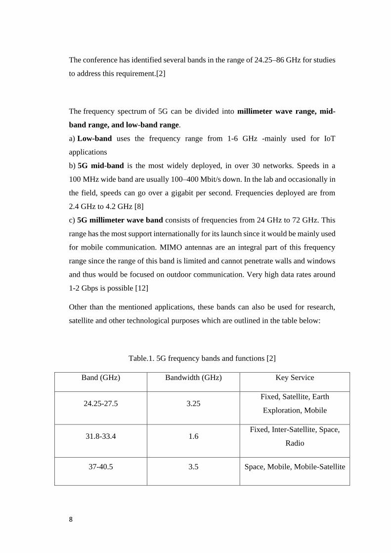
The conference has identified several bands in the range of 24.25–86 GHz for studies
to address this requirement.[2]
The frequency spectrum of 5G can be divided into millimeter wave range, mid-
band range, and low-band range.
a) Low-band uses the frequency range from 1-6 GHz -mainly used for IoT
applications
b) 5G mid-band is the most widely deployed, in over 30 networks. Speeds in a
100 MHz wide band are usually 100–400 Mbit/s down. In the lab and occasionally in
the field, speeds can go over a gigabit per second. Frequencies deployed are from
2.4 GHz to 4.2 GHz [8]
c) 5G millimeter wave band consists of frequencies from 24 GHz to 72 GHz. This
range has the most support internationally for its launch since it would be mainly used
for mobile communication. MIMO antennas are an integral part of this frequency
range since the range of this band is limited and cannot penetrate walls and windows
and thus would be focused on outdoor communication. Very high data rates around
1-2 Gbps is possible [12]
Other than the mentioned applications, these bands can also be used for research,
satellite and other technological purposes which are outlined in the table below:
Table.1. 5G frequency bands and functions [2]
Band (GHz) Bandwidth (GHz) Key Service
24.25-27.5 3.25 Fixed, Satellite, Earth
Exploration, Mobile
31.8-33.4 1.6 Fixed, Inter-Satellite, Space,
Radio
37-40.5 3.5 Space, Mobile, Mobile-Satellite
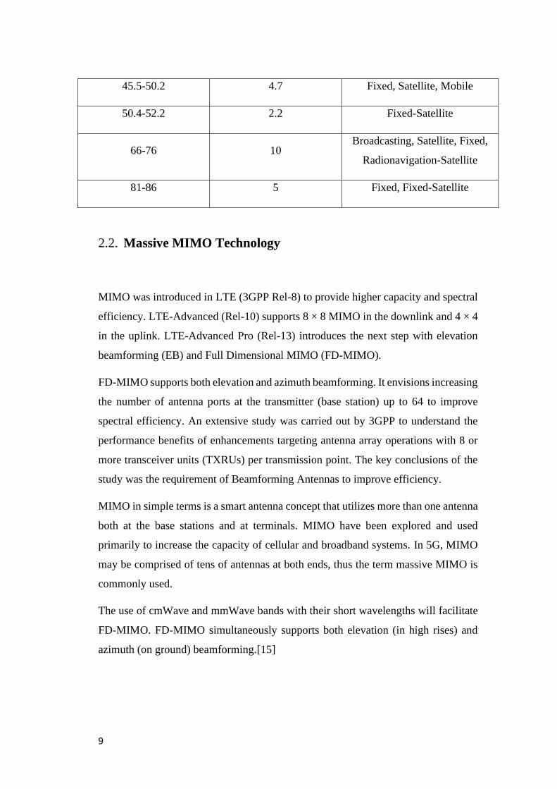
9
45.5-50.2 4.7 Fixed, Satellite, Mobile
50.4-52.2 2.2 Fixed-Satellite
66-76 10 Broadcasting, Satellite, Fixed,
Radionavigation-Satellite
81-86 5 Fixed, Fixed-Satellite
2.2. Massive MIMO Technology
MIMO was introduced in LTE (3GPP Rel-8) to provide higher capacity and spectral
efficiency. LTE-Advanced (Rel-10) supports 8 × 8 MIMO in the downlink and 4 × 4
in the uplink. LTE-Advanced Pro (Rel-13) introduces the next step with elevation
beamforming (EB) and Full Dimensional MIMO (FD-MIMO).
FD-MIMO supports both elevation and azimuth beamforming. It envisions increasing
the number of antenna ports at the transmitter (base station) up to 64 to improve
spectral efficiency. An extensive study was carried out by 3GPP to understand the
performance benefits of enhancements targeting antenna array operations with 8 or
more transceiver units (TXRUs) per transmission point. The key conclusions of the
study was the requirement of Beamforming Antennas to improve efficiency.
MIMO in simple terms is a smart antenna concept that utilizes more than one antenna
both at the base stations and at terminals. MIMO have been explored and used
primarily to increase the capacity of cellular and broadband systems. In 5G, MIMO
may be comprised of tens of antennas at both ends, thus the term massive MIMO is
commonly used.
The use of cmWave and mmWave bands with their short wavelengths will facilitate
FD-MIMO. FD-MIMO simultaneously supports both elevation (in high rises) and
azimuth (on ground) beamforming.[15]
10
The Massive MIMO technology can bring at least ten-fold improvements in area
throughput by increasing the spectral efficiency (bit/s/Hz/cell), while using the same
bandwidth and density of base stations as in current networks.[15]
Transmissions can be parallel by having multiple transmit antennas and multiple
receive antennas. There are two distinct cases:
1. Point-to-point MIMO where a Base Station (BS) with multiple antennas
communicates with a single user terminal having multiple antennas.
2. Multi-user MIMO where a BS with multiple antennas communicates with
multiple user terminals, each having one or multiple antennas.[17]
Multi-user MIMO is found to be the more attractive solution due to lesser number of
antennas and higher efficiency.[18]
The working of multi-user MIMO can be explained as a base station with M antennas
communicating with K single user terminals, each having multiple antennas. The
multiplexing at BS ensures that only one data stream per user is occupying the
downlink and also receives only one data stream per user in its uplink parallelly. As
mentioned before, 5G uses a TDD frame design since there is the added benefit of
scalability in downlink data communication compared to FDD even though uplink
provides same performance in downlink and uplink.[17]
2.2.1. mm-Wave with Massive MIMO
The propagation loss for mmWave transmission is quite large due to the high
frequency and corresponding low wavelength of the signals that therefore limit its
range of transmission. Therefore, mmWave transmission is more suitable for small
cells for data rate and dense user scenarios. To compensate for the propogation losses,
high gain and directivity is required for the designed arrays at both base stations and
user terminals. The MIMO technology consists of using antenna arrays with a large
number of elements, the scale of the array being the cause of high gain. Each element
also needs to be precisely beam-directed in order to obtain the added-up signal at
11
destination. The larger the number of elements, the greater the requirement of proper
beam-steering. For example, a size of 66mm by 66mm may accommodate 1024
antenna elements can form a main beam as narrow as 3°. [17]
The directivity of a beam formed by an array can be sensitive to azimuthal and
elevation angles. Additionally, mmWave transmission link will be sensitive to angle
changes in departure and arrival. The importance of a directed beam is much higher
in the millimeter wave scenario as compared to say, a sub-6 GHz range ( low band)
since the losses are much higher in mm-wave range and the beams in the low-band
range can also be much wider since angle variation is compensated by high range and
gain. For mathematical modelling of mm-range frequency antennas also, the beam
angles thus become necessary.[17]
As a result, comes the requirement of beamforming and beamsteering antenna arrays.
12
2.3. Beamforming and Beamsteering
2.3.1. Beamforming - definition and principle
Beamforming is the formation of a single targeted signal beam by combining signals
at same phase and wavelength from a group of radiating elements in a defined manner
that is more targeted and stronger than a single signal. [21]
mmWave frequency antennas as mentioned before enjoy the advantage of having a
higher bandwidth but suffer from various propogation losses that microwave signals
do not, which are as follows:
1. Path loss: As the term suggests, the loss incurred in the signal as it travels a
distance. The path loss is higher for higher frequencies as per Frii’s law.
2. Diffraction and blockage: High frequency mmWave signals have limited range
and thus cannot penetrate walls, buildings and other solid objects, thus are limited in
outdoor applications.
3. Rain attenuation: Atmospheric effects like rain attenuation become a real problem
in mmWave communication as the magnitude of such attenuation is greater for these
signals over microwave signals
4. Atmospheric absorption: Another effect of atmospheric interaction is the
absorption of the waves due to oxygen that is greater for mmWave signals over
microwave signals as per field measurements.
5. Foliage loss: In densely wooded areas, the radio link can be obstructed by trees
that will interfere in signal quality.
All these factors contribute to the overall losses of mmWave signals being larger than
those of microwave signals. Fortunately, the small wavelengths of mmWave signals
enable a large number of antenna elements to be placed in the same physical
antenna area thereby providing high spatial processing gains that can theoretically
compensate for at least the corresponding isotropic path loss. [22]
A narrower beam can be formed by increasing the number of radiating elements that
make up the antenna array. A negative effect of beamforming is the side lobes. These
are the excessive or unwanted radiation of the signal that forms the main lobe in
13
different directions. Poorly designed antenna arrays would cause an excessive
interference to beamformed main beam by way of the signal’s side lobe. Thus,
increasing the number of radiating elements will result in a narrower and more
directive beam with lesser sidelobe which is the essence of the MIMO technique.[21]
2.3.2. Beamsteering and Beam Switching
In the cellular communication scenario, beam steering is achieved by adaptively
updating the phase of the input signal on all radiating elements constituting the BS
array. Phase shifting allows the signal to be targeted at a specific receiver. An antenna
system can be such that it consists of radiating elements creating a single beam with
a common frequency steered in a particular direction. Different frequency beams can
also be steered in different directions to serve different users. The direction a signal
is sent is determined by the base station and is updated dynamically as the user moves,
effectively tracking the user. If a beam cannot track a user, the endpoint may switch
to a different beam.[21]
Beamforming consists of applying discrete phase shifts to each antenna element
forming the antenna array effectively shaping the beam and providing individual
control of the direction of a transmitted beam.[23]
2.3.3. Beamforming techniques
Beamforming techniques can be subclassified as: RF/analogue, digital, or hybrid
beamforming.
a) RF/Analog beamforming: Each element of an antenna array produces a signal that
is individually given a time delay using a phase shifter. This method of beamforming
is relatively cheap and low power when compared to digital beamforming [24]. The
challenge faced by this method is the frequency dependence of phase shifters thereby
limiting high-bandwidth applications.
14
b) Digital beamforming: The same beamforming principles as for the RF case are
applied to a digitized signal. An ADC samples the sinusoidal signals from each
element of the array. It is however costlier and more power hungry.
c) Hybrid beamforming: As the name suggests, it is a combination of RF and Digital
beamforming methods. The first conversion is done by the RF beamformer in
providing phase shifts to each signal. The 2nd section is controlled by the Digital
section that takes care of the sampling as well as down-conversion to baseband. This
combination enhances performance of the system as well as allows multiple channels
to be accommodated simultaneously.[24]
2.3.4. Beamsteering techniques
After forming the desired beam, various methods of beamsteering is required to direct
the beam to a specific user from base station.
The different types of beamsteering methods practically used are outlined:
1. Mechanical steering
This consists of physically turning the antenna to face the desired direction.
Mechanical steering is often performed by means of electric motors. Mechanical
steering is highly effective since it maintains the gain of the antenna and offers
flexibility in the steering range of the antenna.
Mechanical steering becomes undesirable and difficult when we consider factors such
as antenna size, weight, and weather conditions. Recently, MEMS devices have been
used to implement mechanical steering, they offer improved speed of scanning
compared to manually steered arrays as well as low losses to the system. Steering
speed is usually limited by weather and other mechanical conditions and thus the
application is usually to areas where high speed operation is not required. Also,
rotating mechanisms are prone to mechanical failure due to fatigue and wearing of
moving parts.[24]
15
2. Phase shifters/ phased array antennas:
Phased arrays are a very popular method of beamsteering and is the electronic
steering of the beam by providing phase shifts to each antenna element. Its range is
limited by the pattern of the array and circuit design. It has the advantage of high
directivity, multiple beamforming (one at a time in different directions), fast scanning
when compared to mechanical steering due to its electronic circuitry, and spatial
filtering.[24]
A PIN diode or switching MESFET is used to switch between two or more different
lengths of transmission line. The length of each transmission line is calculated in such
a way to achieve the desired amount of phase shift as the signal travels through the
line.
The drawback observed is that the circuitry is highly influenced by noise and incurs
heavy losses to the device. The insertion loss is also high for these devices.[24]
3. Reflectarray antennas:
A reflectarray is formed from the combination of a reflector and an array antenna. In
place of a reflector, various reflector elements are also used in a reflectarray antennas.
Due to small antenna elements, the reflectarray can be designed to be lightweight. It
also has the advantage of generating multiple beams and can dynamically steer its
radiation pattern.[24]
It, however, has the disadvantage of having high insertion losses due to phase shifters.
The phase shift and thus scan angle of the beam is also predetermined during design
stage thus the range is limited and cannot offer continuous scanning. With increasing
number of elements, the complexity and cost of reflectarray increases.
4. Parasitic Steering by Yagi Uda Antennas
The Yagi-Uda antenna is made up of a driver or radiating element and multiple
passive or parasitic elements. The passive elements obtain energy through
electromagnetic coupling from the driver element. Various configurations of antenna
have been proposed in literature, these include Electrically Steerable Passive Array
16
Radiators (ESPAR), Circular Switched Parasitic Array (CSPA), and disk-loaded
monopole array antennas.[24]
As in the case of the phased array, the beam-steeering angles are predefined but the
insertion losses are much lower for these types of antennas.
5. Traveling Wave Antennas
Antennas can be broadly classified as standing wave (resonant) antennas or traveling
wave antennas. Resonant antennas consist of open-ended wires that form standing
waves through reflection. The pattern formed depends on design of both radiating
part and matched impedance.[24]
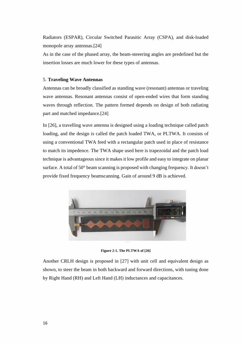
In [26], a travelling wave antenna is designed using a loading technique called patch
loading, and the design is called the patch loaded TWA, or PLTWA. It consists of
using a conventional TWA feed with a rectangular patch used in place of resistance
to match its impedence. The TWA shape used here is trapezoidal and the patch load
technique is advantageous since it makes it low profile and easy to integrate on planar
surface. A total of 50° beam scanning is proposed with changing frequency. It doesn’t
provide fixed frequency beamscanning. Gain of around 9 dB is achieved.
Figure 2-1. The PLTWA of [26]
Another CRLH design is proposed in [27] with unit cell and equivalent design as
shown, to steer the beam in both backward and forward directions, with tuning done
by Right Hand (RH) and Left Hand (LH) inductances and capacitances.
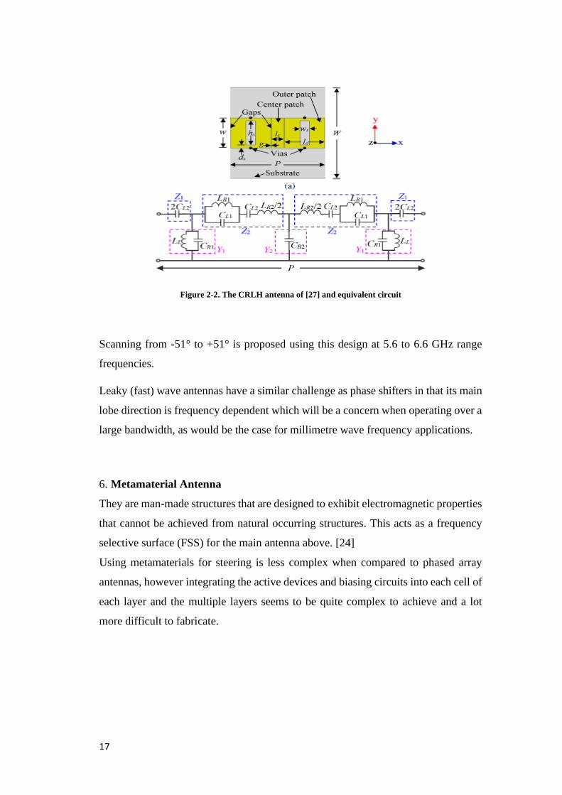
17
Figure 2-2. The CRLH antenna of [27] and equivalent circuit
Scanning from -51° to +51° is proposed using this design at 5.6 to 6.6 GHz range
frequencies.
Leaky (fast) wave antennas have a similar challenge as phase shifters in that its main
lobe direction is frequency dependent which will be a concern when operating over a
large bandwidth, as would be the case for millimetre wave frequency applications.
6. Metamaterial Antenna
They are man-made structures that are designed to exhibit electromagnetic properties
that cannot be achieved from natural occurring structures. This acts as a frequency
selective surface (FSS) for the main antenna above. [24]
Using metamaterials for steering is less complex when compared to phased array
antennas, however integrating the active devices and biasing circuits into each cell of
each layer and the multiple layers seems to be quite complex to achieve and a lot
more difficult to fabricate.
18
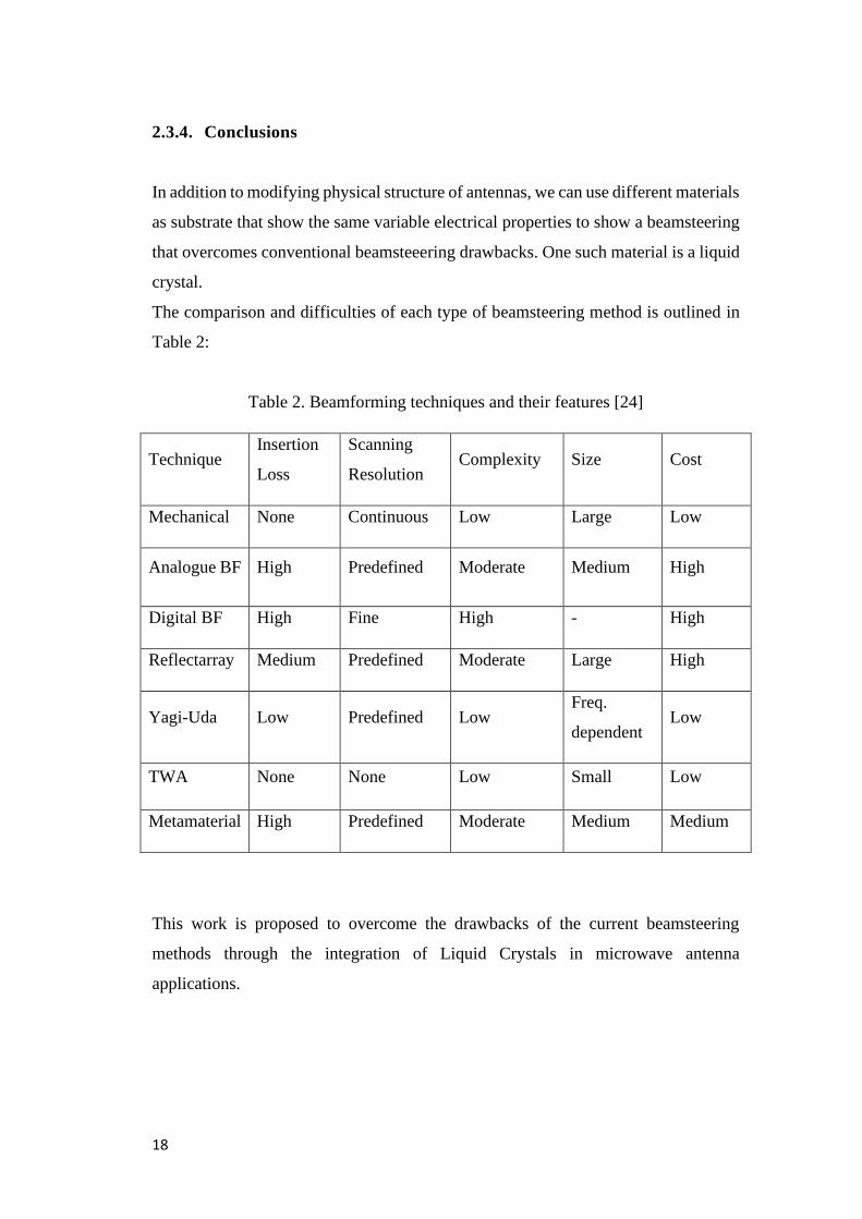
2.3.4. Conclusions
In addition to modifying physical structure of antennas, we can use different materials
as substrate that show the same variable electrical properties to show a beamsteering
that overcomes conventional beamsteeering drawbacks. One such material is a liquid
crystal.
The comparison and difficulties of each type of beamsteering method is outlined in
Table 2:
Table 2. Beamforming techniques and their features [24]
This work is proposed to overcome the drawbacks of the current beamsteering
methods through the integration of Liquid Crystals in microwave antenna
applications.
Technique Insertion
Loss
Scanning
Resolution Complexity Size Cost
Mechanical None Continuous Low Large Low
Analogue BF High Predefined Moderate Medium High
Digital BF High Fine High - High
Reflectarray Medium Predefined Moderate Large High
Yagi-Uda Low Predefined Low Freq.
dependent Low
TWA None None Low Small Low
Metamaterial High Predefined Moderate Medium Medium
19
2.4. Liquid Crystals
2.4.1. Physical Properties and Behaviour
Liquid crystals are materials showing mesophases between crystalline solid and
isotropic liquid [29]. The constituents are elongated rod-like (calamitic) or disk-like
(discotic) molecules. The anisotropy in its dielectric permittivity is manipulated for
use in modern electronic applications. This change in permittivity is the result of
reorientation of the constituent molecules in the presence of electric field. Such
Liquid Crystal materials are called Nematic LCs or NLCs. Its Achilles heel is a slow
(millisecond) relaxation from the field-on to the field-off state. [30]
Nematic liquid crystals (NLCs) have revolutionized the way optical information is
presented and processed [30]. NLCs act as an electro-optic medium and one
important aspect that makes this possible is the long-range order in its orientation.
NLC molecules are of an anisometric shape, in most cases resembling an elongated
rod or a disc. Based on shape, LCs are characterized as calametic (rod shaped),
discotic and newly discovered bent core or banana shaped.
The chemical property of a Liquid Crystal molecule can be observed to show a rigid
core consisting of polar groups. They show strong dipole-dipole or dipole-induced-
dipole bonds or hydrogen bonds between them. In some cases, they show both. In
most cases, the intermolecular interactions are due to the presence of polar or
polarizable groups. Commonly found constituents are aromatic rings, multiple carbon
bonds and oxygen-nitrogen bonds. Moreover, many liquid crystals are composed of
molecules with two similar halves connected by a unit having a multiple bond. [32]
The size of the molecules is typically a few nanometers (nm). Since they possess long
range order due to their rod like shape, it is common to see the ratio between the
length and width (thickness) of the molecule to be 5 or greater. In addition to
positional order, they may possess orientational order. In order to exhibit this
20
property, they have a rigid core with a flexible body. eg: A typical calamitic (rod
shaped) liquid crystal molecule is 40-nPentyl-4-cyano-biphenyl and is abbreviated as
5CB. It consists of a biphenyl, which is the rigid core, and a hydrocarbon chain which
is the flexible tail. [33]
If the molecule is completely flexible, it will not have orientational order. If it is
completely rigid, it will transform directly from isotropic liquid phase at high
temperature to crystalline solid phase at low temperature. With balanced rigid and
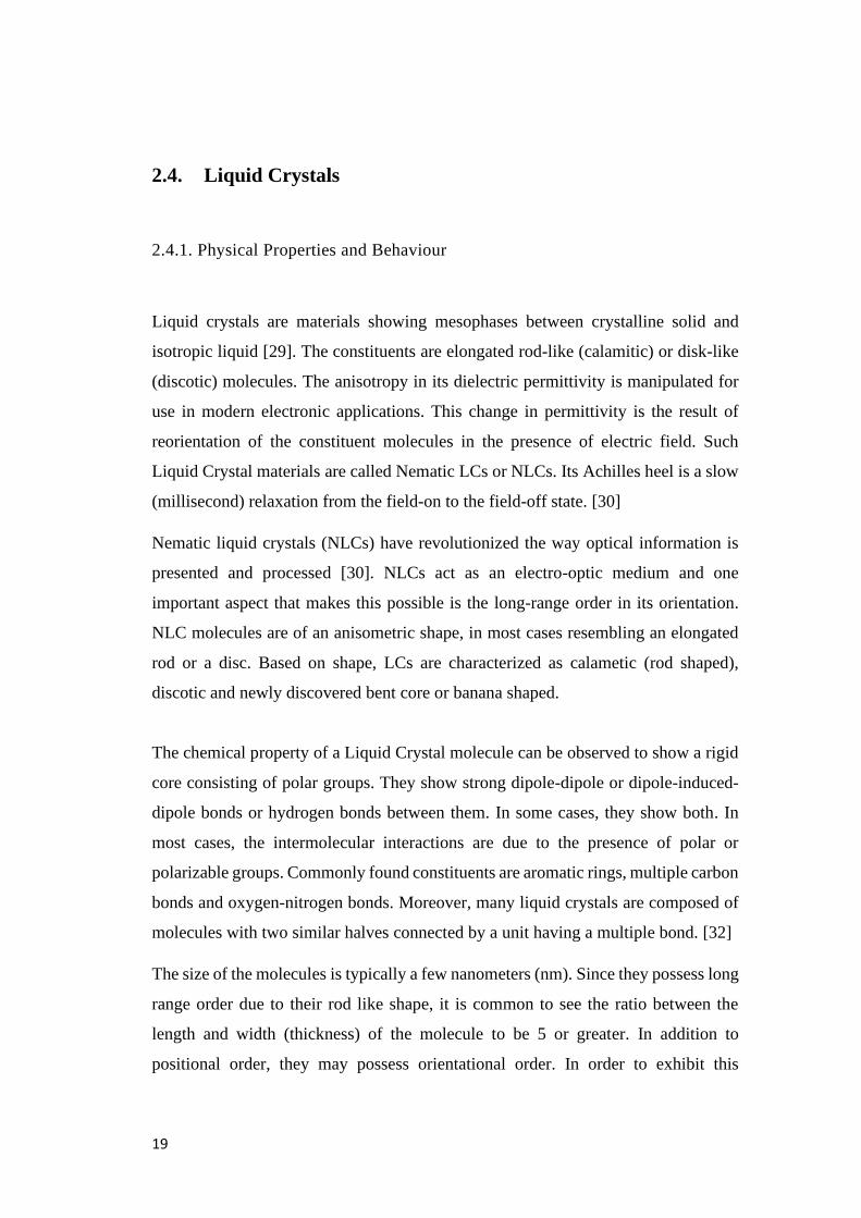
flexible parts, the molecule exhibits liquid crystal phases.
The variety of phases that may be exhibited by rod-like molecules are shown in figure
below:
Figure 2-3. Temperature dependant phases of calamitic LCs [33]
The average direction of the long molecular axis is denoted by n, which is a unit
vector called the liquid crystal director.
The transition temperature of each type of LC varies and different combination of
materials can be chosen to form the crystal depending on application requirement. It
can vary from 10-240°C.
Temperature dependency of most commercially available liquid crystals indicate a
transition temperature from cholesteric to nematic phase at 38 - 55◦ C, while
transition points of up to 170 ◦ C is also possible for certain cases. The crystals are
also found to be electronically stable up to 113◦ C in all cases.
For using LCs in experimental setup, the initial state of molecular orientation that is
parallel to a surface is achieved through a process called anchoring. 2 types of
21
anchoring are possible-called homogeneous and homeotropic anchoring.
Homogeneous anchoring consists of mechanically rubbing the surface of a substrate
such that the microgrooves created due to rubbing helps align the LC material
applied. Homeotropic anchoring consists of using chemicals like lecithin, silane etc
that act as surfactant to attach the polar part of the LC molecule to the surface and
thus aligning the hydrocarbon tail to point outwards.[33]
2.4.2. Reaction to external Electric Field
The most useful property of a liquid crystal is their ready reactance to electric field
that causes changes in the LC structure. The molecular orientation is easily changed
by the application of relatively low voltage (<10V) across the material. Due to their
high resistances, they consume less power and act as dielectric or ferroelectric media.
When the liquid crystals reorient, their optical properties change dramatically because
of their large birefringences.
Liquid crystals in their unexcited state has 0 dipole moment in the bulk. When an
electric field is applied, they start to obtain individual dipole moments and reorient
such that total free energy of the system is minimized.[29]
The difference in permittivity caused by change in orientation of rod-like LC
molecules at 0 V and above a threshold voltage Vth can be defined in terms of
dielectric anisotropy. The dielectric anisotropy of a Liquid Crystal is defined as the
change in the value of electric permittivity along the parallel and perpendicular
direction of applied electric field. This permittivity is therefore a vector that can be
depicted in matrix form. The difference between 𝜀// and 𝜀⊥ is depicted as Δε which
is used to define further properties of the material. It is found that the LC molecules
orient to applied field to minimize the net energy of the system. For molecules with
Δε > 0, molecular orientation parallel or anti-parallel to field reduces the energy. For
molecules with Δε < 0, the molecular orientation perpendicular to field minimizes
energy. As such, the material behaves to external field as per its permittivity
properties.
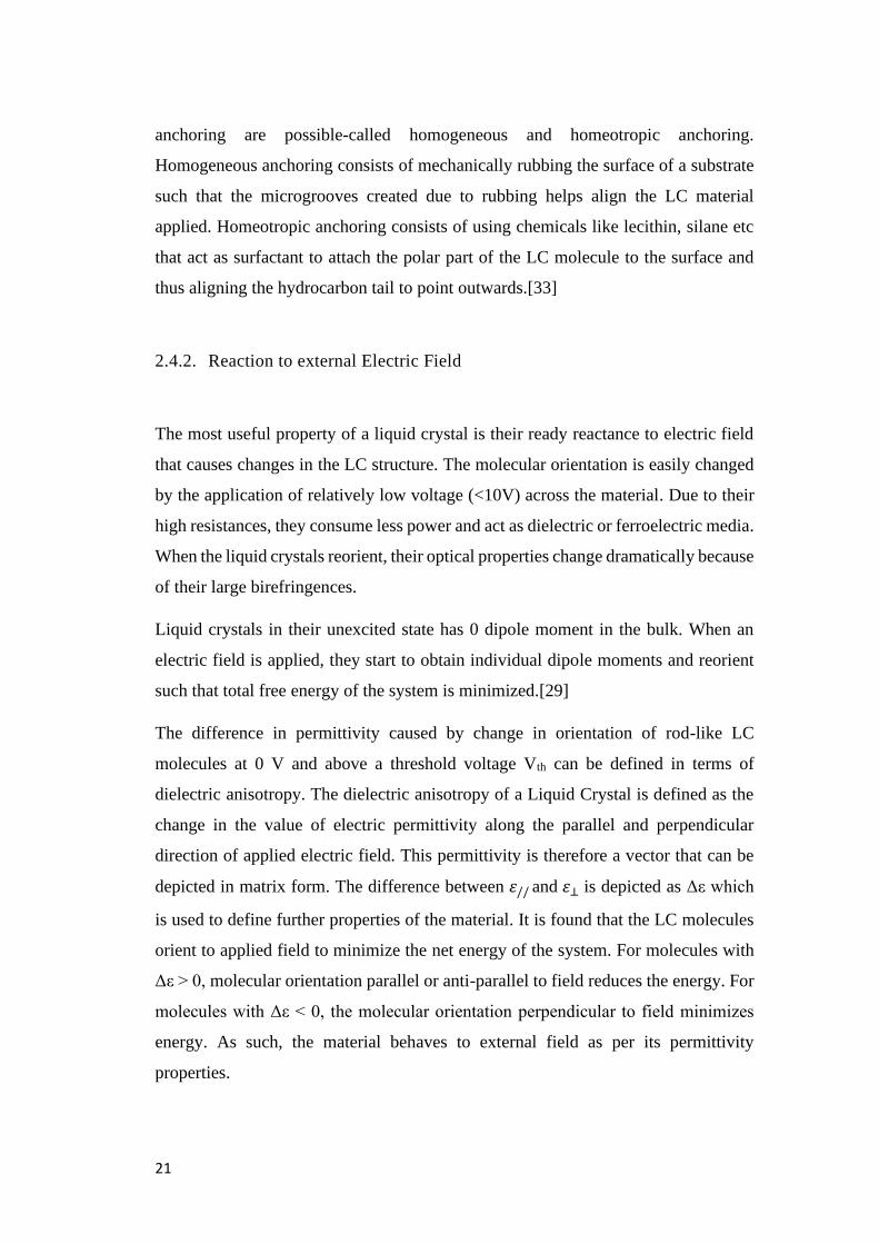
22
The process of reorientation of LC director to minimize free energy of a system when
an electric field is applied is called Frederickz transition. The initial orientation of LC
molecules is dependant on the type of anchoring applied to the surface and the
changes to orientation occur due to applied field. [29] The theoretical depiction of
LC properties with electric field can be described using equations as below:
For a uniaxial liquid crystal when the liquid crystal director is n= {nx, ny, nz},
nx = cosθ, ny = sinθ and nz = 0, the dielectric tensor is
Figure 2-4. Anchoring and behavior of LC with applied DC voltage [35]
23
𝛆↔ = (
𝛆⊥ + ∆𝛆 𝐜𝐨𝐬𝟐Ɵ ∆𝛆 𝐬𝐢𝐧 𝛉 𝐜𝐨𝐬𝛉 𝟎
∆𝛆 𝐬𝐢𝐧 𝛉 𝐜𝐨𝐬𝛉 𝛆⊥ + ∆𝛆 𝐬𝐢𝐧𝟐Ɵ 𝟎𝟎 𝟎 𝛆⊥
) (2- 1)
where θ is the angle made by the LC director with z axis and Δε = ε|| - εꞱ.
At V=0, when director angle is 0,
𝛆
↔ = (
𝛆|| 𝟎 𝟎
𝟎 𝛆⊥ 𝟎𝟎 𝟎 𝛆⊥
) (2- 2)
At V= Vth , where director orients at 90◦ assuming Δε < 0,
𝛆
↔ = (
𝛆⊥ 𝟎 𝟎𝟎 𝛆|| 𝟎
𝟎 𝟎 𝛆⊥
) (2- 3)
Electric field can also affect the orientational order of the crystal. The transition
temperature for conversion from isotropic to nematic and then to smectic phases can
be changed by changing field strength outlined by the Maier-Saupe and Landau-
deGennes theories.[29]
Some examples of LCs are: 5CB, 1,2-Dihexyloxybenzene, 1-Dodecylpyridinium
chloride hydrate, 4-Ethoxybenzoic acid, 4-Phenylbenzonitrile etc. which are all
commercially available for purchase.
2.4.3. LC Based Beamteering techniques
In [36], a meanderline based design using inverted microstrip topology is presented
for beamsteering using a liquid crystal substrate and Dielectric Resonator Antennas
(DRA)’s. the LC layer is sandwiched between meanderline layer and slot antenna
layer to enable scanning with applied DC voltage. The work proposed a meanderline
FOM of 70°/dB and a gain of 12 dB at 10 GHz.
Individual feed biasing is required for its operation. DRA’s also present a more
complicated mechanism of antenna tuning.
24
In [37], a LC based reflectarray design is presented for operation at 77 GHz. An open
WR-10 waveguide feed is used as the feed method for 16 x 16 unit cells with LC
layer below them. A scanning from -25° to 25° is proposed to be achieved with 8 dB
sidelobe level.The design requires good integration with open waveguide and patch
array to achieve satisfactory power levels.
[38] proposes an Slot Integrated Waveguide (SIW) feed based design using slots like
in an LWA with a Wilkinson power divider and with LC phase shifter.
The structure is designed to operate at 11.28-12.5 GHz. It shows a beamsteering
capability of -11° to 11°. The LC used is Merck’s GT3-23001 with permittivity
change possible from ε=2.56 to 3.28.
In [39], a patch antenna and meanderline based LC phase shift design is covered.
This unique design makes use of the electrical length change property by changing
the permittivity of the LC used (ε=0.79 to ε=2.78) to obtain a maximum differential
phase shift of 38°, but steering of the main beam is by 9°.
Another unique CRLH antenna is proposed in [40] that claims a beamsteering range
from -23° to 21°.
The 3-layer design poses some design challenges. It operates at 11.8-12 GHz and is
able to scan the beam with frequency as well as at fixed frequency using tunable LC
layer.
Later in this work, we consider different types of antennas with LC layer to see which
gives best performance.
Conclusion
LC layer shows a method to control beam direction of antennas without encountering
the losses in other beamsteering methods, for example, there is no material losses,
additional hardware for steering, expensive electronics required to achieve the
variable material properties of LC. A low DC voltage is enough to achieve this by the
use of small batteries. There is also no additional modifications to be made to antenna
25
structure since the material is easily integrable to all planar structures. Most literature
on conventional beamsteering techniques encounter the problems of limited range,
additional hardware, switching speed, bandwidth, scanning range, insertion loss and
frequency dependance of circuits, which can be overcome by Liquid Crystal based
techniques. LC based beamsteering techniques have also not covered the application
of the material on conventional array techniques and how the performance of those
can be improved using this beamscanning method. There were 2 distinct techniques
that were of particular interest in the review, being the Patch loaded TWA and the
CRLH designs, both of which can be easily accommodated with the LC layer and the
DC bias line. In addition, all types of existing antenna configurations can be explored
to see the behaviour with the unique Liquid Crystal.
26
CHAPTER 3
MEANDERLINE FEED AND INTERDIGITATED FEED COMPARISON
WITH LC LAYER
3.1. Introduction
The phase shifting property of Liquid Crystal is analysed using a simple feed structure
that makes use of a cavity filled with liquid crystal inside a substrate. Commercially
available Liquid crystals that can operate at high frequencies like 5CB, GT3-2001
shows permittivity between 1.5 (ε⊥) and 3.9 (ε//), with loss tangents from 0.004 to
0.03.
For this application, a new material was defined as LC with a loss tangent of 0.02 and
permittivity changing from 2.5 to 3.5, which is a range that is practically achievable
with DC voltages below 5V. The substrate used is Rogers RO4350B whose electrical
permittivity is 3.48, loss tangent of 0.0037 and thermal conductivity of 0.62 W/K/m.
The substrate has height of 0.503mm. A cavity of 0.25mm depth is made inside this
substrate. It is filled with LC of changing permittivity. The material data of
commercially available LCs were compared to define a new material with εr defined
as 2.5 with tan δ =0.006 and at higher values of DC voltage εr of 3.5 with tan δ=0.002.
A ground plane of 0.017mm thickness is below the structure.
Impedence of 50 ꭥ is obtained using microstrip line of width 1.44mm. Quarter wave
matching is done using λ/4 length line ie, 1.45mm long with width 0.4mm. Two types
of feeds were compared to see which shows best phase tuning range: Meanderline
feed and Interdigitated feed.
3.2. Meanderline feed
27
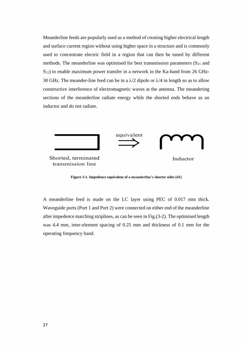
Meanderline feeds are popularly used as a method of creating higher electrical length
and surface current region without using higher space in a structure and is commonly
used to concentrate electric field in a region that can then be tuned by different
methods. The meanderline was optimised for best transmission parameters (S21 and
S12) to enable maximum power transfer in a network in the Ka-band from 26 GHz-
30 GHz. The meander-line feed can be in a /2 dipole or /4 in length so as to allow
constructive interference of electromagnetic waves at the antenna. The meandering
sections of the meanderline radiate energy while the shorted ends behave as an
inductor and do not radiate.
Figure 3-1. Impedence equivalent of a meanderline’s shorter sides [41]
A meanderline feed is made on the LC layer using PEC of 0.017 mm thick.
Waveguide ports (Port 1 and Port 2) were connected on either end of the meanderline
after impedence matching striplines, as can be seen in Fig.(3-2). The optimised length
was 4.4 mm, inter-element spacing of 0.25 mm and thickness of 0.1 mm for the
operating frequency band.
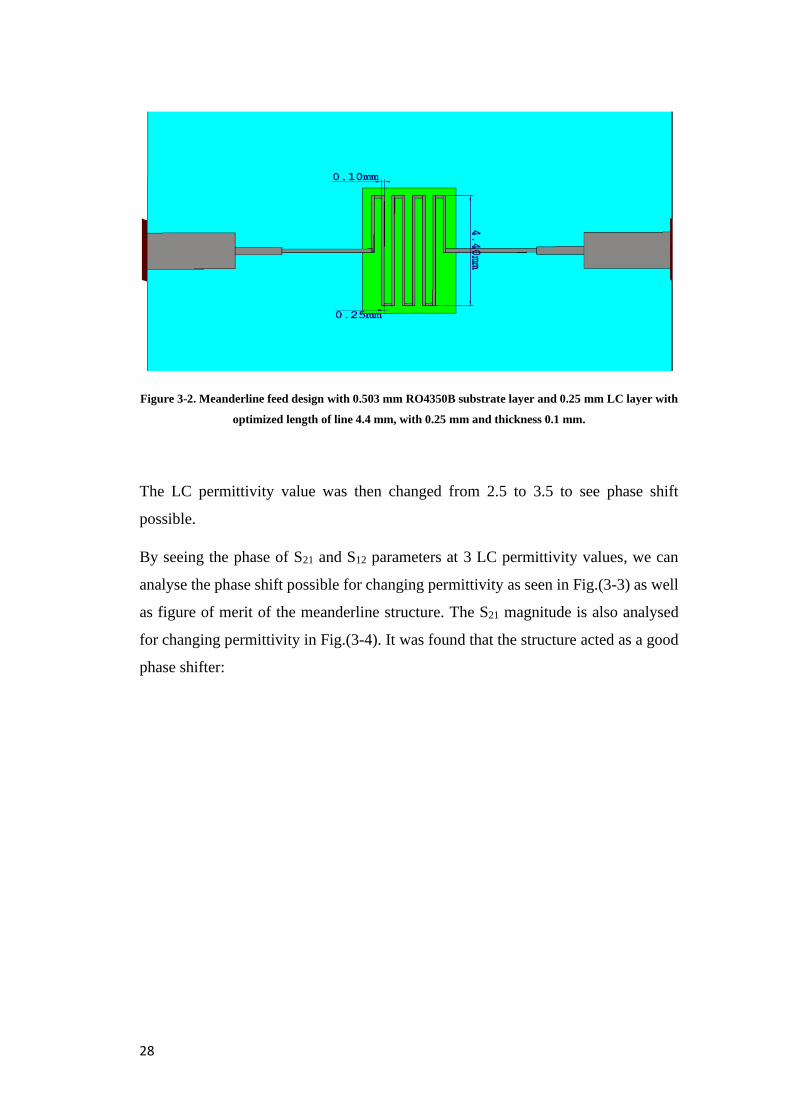
28
Figure 3-2. Meanderline feed design with 0.503 mm RO4350B substrate layer and 0.25 mm LC layer with
optimized length of line 4.4 mm, with 0.25 mm and thickness 0.1 mm.
The LC permittivity value was then changed from 2.5 to 3.5 to see phase shift
possible.
By seeing the phase of S21 and S12 parameters at 3 LC permittivity values, we can
analyse the phase shift possible for changing permittivity as seen in Fig.(3-3) as well
as figure of merit of the meanderline structure. The S21 magnitude is also analysed
for changing permittivity in Fig.(3-4). It was found that the structure acted as a good
phase shifter:
29
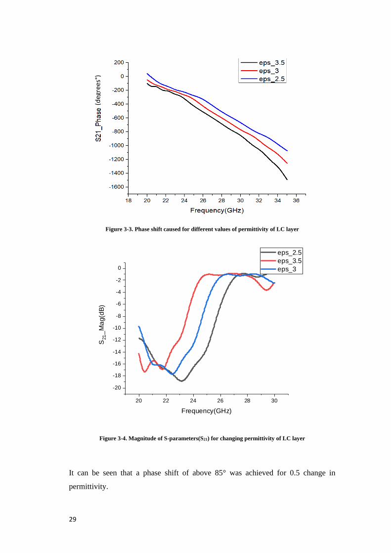
Figure 3-3. Phase shift caused for different values of permittivity of LC layer
Figure 3-4. Magnitude of S-parameters(S21) for changing permittivity of LC layer
It can be seen that a phase shift of above 85° was achieved for 0.5 change in
permittivity.
20 22 24 26 28 30
-20
-18
-16
-14
-12
-10
-8
-6
-4
-2
0
S21_
Ma
g(d
B)
Frequency(GHz)
eps_2.5
eps_3.5
eps_3
(deg
rees
°)
30
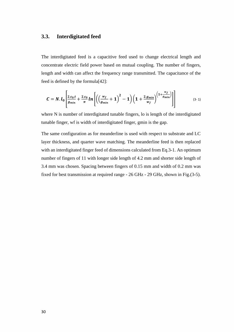
3.3. Interdigitated feed
The interdigitated feed is a capacitive feed used to change electrical length and
concentrate electric field power based on mutual coupling. The number of fingers,
length and width can affect the frequency range transmitted. The capacitance of the
feed is defined by the formula[42]:
𝑪 = 𝑵. 𝒍𝟎 [𝟐.𝜺𝟎.𝒕
𝒈𝒎𝒊𝒏+
𝟐.𝜺𝟎
𝝅𝒍𝒏 [((
𝒘𝒇
𝒈𝒎𝒊𝒏+ 𝟏)
𝟐
− 𝟏) (𝟏 +𝟐.𝒈𝒎𝒊𝒏
𝒘𝒇)
(𝟏+𝒘𝒇
𝒈𝒎𝒊𝒏)
]] (3- 1)
where N is number of interdigitated tunable fingers, lo is length of the interdigitated
tunable finger, wf is width of interdigitated finger, gmin is the gap.
The same configuration as for meanderline is used with respect to substrate and LC
layer thickness, and quarter wave matching. The meanderline feed is then replaced
with an interdigitated finger feed of dimensions calculated from Eq.3-1. An optimum
number of fingers of 11 with longer side length of 4.2 mm and shorter side length of
3.4 mm was chosen. Spacing between fingers of 0.15 mm and width of 0.2 mm was
fixed for best transmission at required range - 26 GHz - 29 GHz, shown in Fig.(3-5).
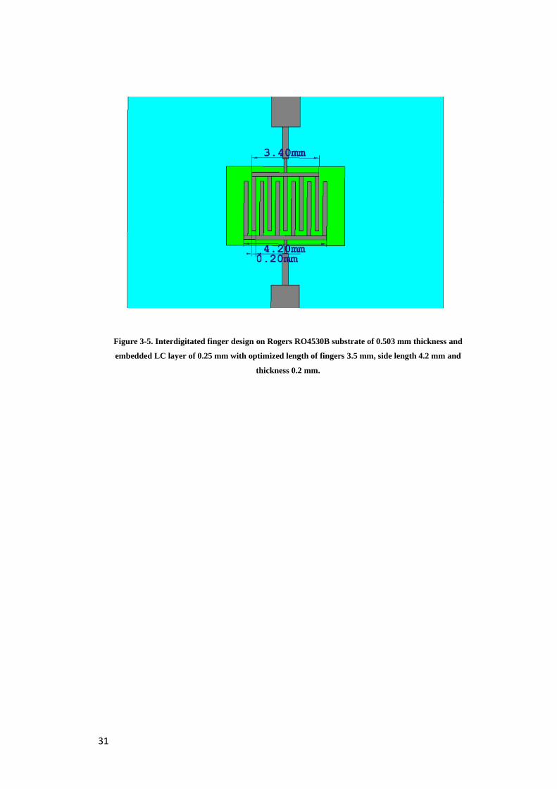
31
Figure 3-5. Interdigitated finger design on Rogers RO4530B substrate of 0.503 mm thickness and
embedded LC layer of 0.25 mm with optimized length of fingers 3.5 mm, side length 4.2 mm and
thickness 0.2 mm.
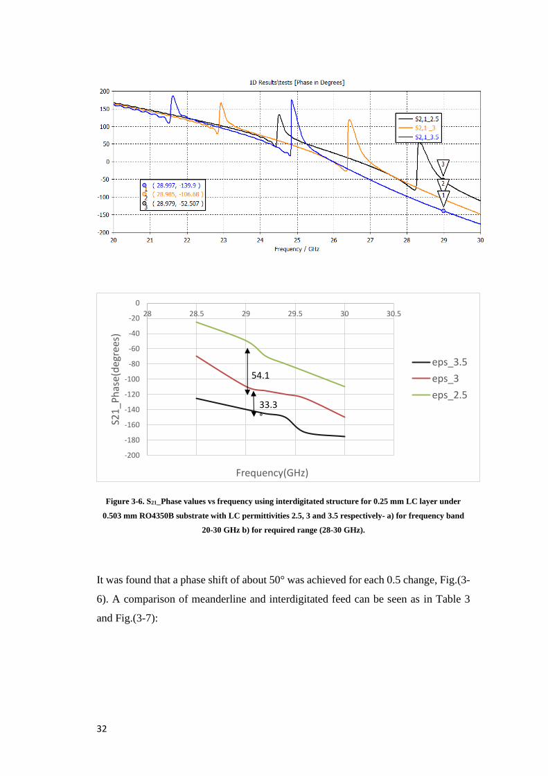
32
Figure 3-6. S21_Phase values vs frequency using interdigitated structure for 0.25 mm LC layer under
0.503 mm RO4350B substrate with LC permittivities 2.5, 3 and 3.5 respectively- a) for frequency band
20-30 GHz b) for required range (28-30 GHz).
It was found that a phase shift of about 50° was achieved for each 0.5 change, Fig.(3-
6). A comparison of meanderline and interdigitated feed can be seen as in Table 3
and Fig.(3-7):
-200
-180
-160
-140
-120
-100
-80
-60
-40
-20
0
28 28.5 29 29.5 30 30.5
S21
_Ph
ase(
deg
rees
)
Frequency(GHz)
eps_3.5
eps_3
eps_2.5
54.1
33.3°
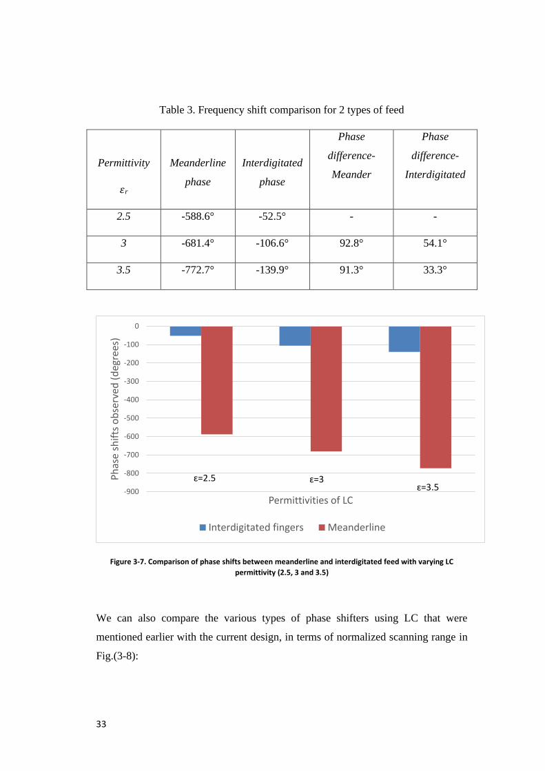
33
Table 3. Frequency shift comparison for 2 types of feed
Permittivity
𝜀r
Meanderline
phase
Interdigitated
phase
Phase
difference-
Meander
Phase
difference-
Interdigitated
2.5 -588.6° -52.5° - -
3 -681.4° -106.6° 92.8° 54.1°
3.5 -772.7° -139.9° 91.3° 33.3°
Figure 3-7. Comparison of phase shifts between meanderline and interdigitated feed with varying LC
permittivity (2.5, 3 and 3.5)
We can also compare the various types of phase shifters using LC that were
mentioned earlier with the current design, in terms of normalized scanning range in
Fig.(3-8):
-900
-800
-700
-600
-500
-400
-300
-200
-100
0
Ph
ase
shif
ts o
bse
rved
(d
egre
es)
Permittivities of LC
Interdigitated fingers Meanderline
ɛ=2.5 ɛ=3ɛ=3.5
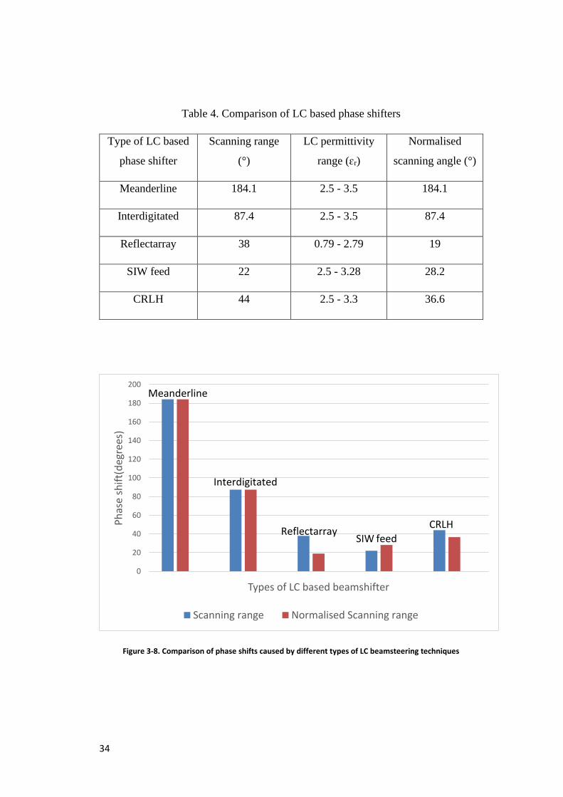
34
Table 4. Comparison of LC based phase shifters
Type of LC based
phase shifter
Scanning range
(°)
LC permittivity
range (ɛr)
Normalised
scanning angle (°)
Meanderline 184.1 2.5 - 3.5 184.1
Interdigitated 87.4 2.5 - 3.5 87.4
Reflectarray 38 0.79 - 2.79 19
SIW feed 22 2.5 - 3.28 28.2
CRLH 44 2.5 - 3.3 36.6
Figure 3-8. Comparison of phase shifts caused by different types of LC beamsteering techniques
0
20
40
60
80
100
120
140
160
180
200
Ph
ase
shif
t(d
egre
es)
Types of LC based beamshifter
Scanning range Normalised Scanning range
Meanderline
Interdigitated
ReflectarraySIW feed
CRLH
35
3.4. Conclusion
In this chapter, the goal was to find the best type of feed network that can be combined
with LC layer to apply in all types of antenna designs. Our candidate feed types were
meanderline feed and interdigitated feed. Both feeding mechanisms were favorable
due to the compact size and large phase shift they could provide with varying
electrical property of their substrate material. To check which of them would provide
more shift, a configuration with embedded LC layer inside a Rogers substrate was
taken, with 2 opposite sides of feed attached with ports to see the angle shift. The
meanderline feed was seen to be the better phase shifter since it has higher value of
phase change for each 0.5 change in permittivity. The interdigitated shifter also shows
a saturation in phase shift at highest permittivity, since change between εr 2.5 to 3 is
higher than between 3 and 3.5.The figure of merit for Interdigitated case is found to
be 29°/dB while meanderline case is 61°/dB. Hence the research proved that a
meanderline feed would be the suitable feed type for the antenna configurations to be
tested in the coming chapters. The design of the LC layer configuration and the
dimensions of both feeds for maximum shift with permittivity change were original
ideas done in this work.
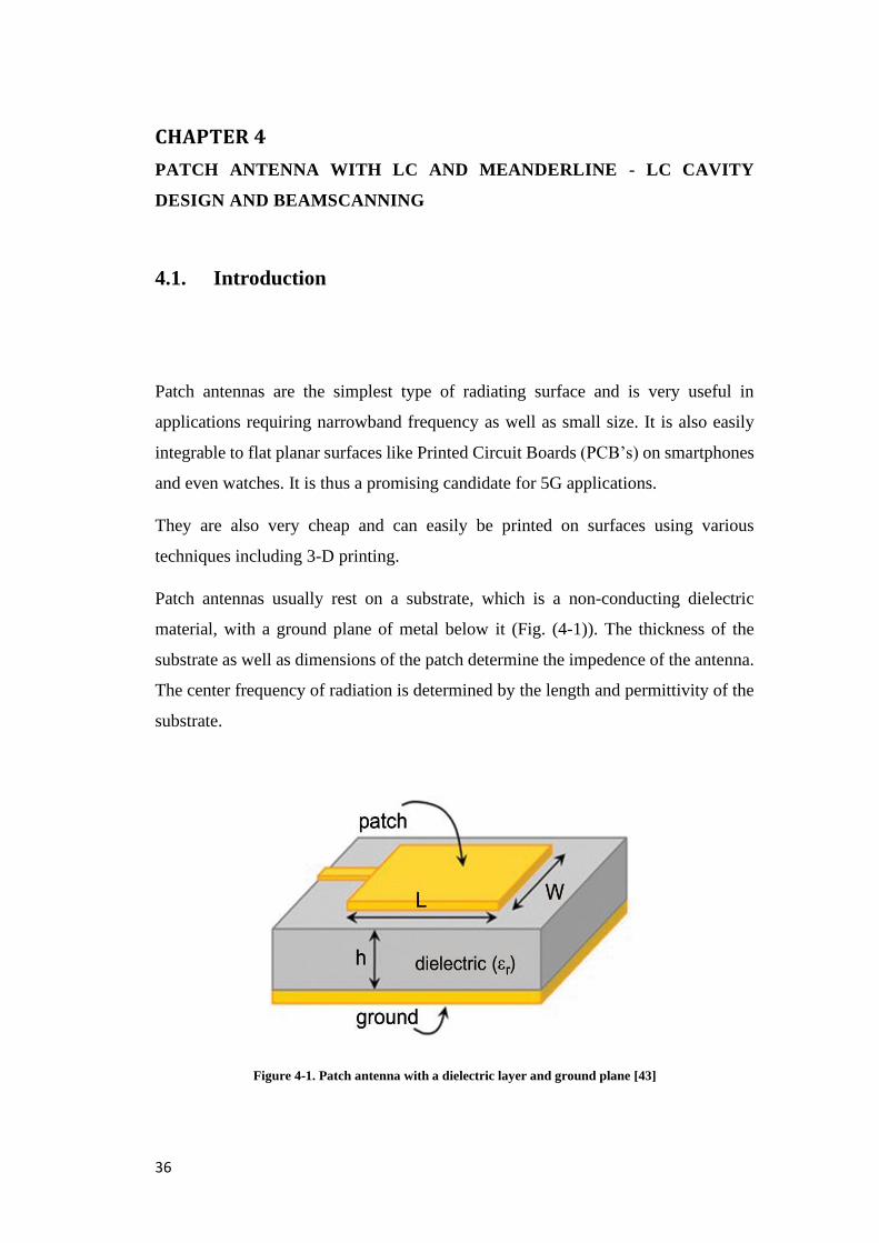
36
CHAPTER 4
PATCH ANTENNA WITH LC AND MEANDERLINE - LC CAVITY
DESIGN AND BEAMSCANNING
4.1. Introduction
Patch antennas are the simplest type of radiating surface and is very useful in
applications requiring narrowband frequency as well as small size. It is also easily
integrable to flat planar surfaces like Printed Circuit Boards (PCB’s) on smartphones
and even watches. It is thus a promising candidate for 5G applications.
They are also very cheap and can easily be printed on surfaces using various
techniques including 3-D printing.
Patch antennas usually rest on a substrate, which is a non-conducting dielectric
material, with a ground plane of metal below it (Fig. (4-1)). The thickness of the
substrate as well as dimensions of the patch determine the impedence of the antenna.
The center frequency of radiation is determined by the length and permittivity of the
substrate.
Figure 4-1. Patch antenna with a dielectric layer and ground plane [43]
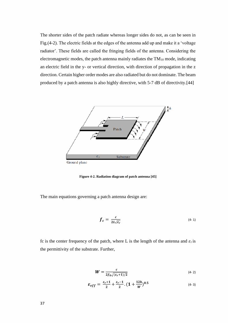
37
The shorter sides of the patch radiate whereas longer sides do not, as can be seen in
Fig.(4-2). The electric fields at the edges of the antenna add up and make it a ‘voltage
radiator’. These fields are called the fringing fields of the antenna. Considering the
electromagnetic modes, the patch antenna mainly radiates the TM10 mode, indicating
an electric field in the y- or vertical direction, with direction of propagation in the z
direction. Certain higher order modes are also radiated but do not dominate. The beam
produced by a patch antenna is also highly directive, with 5-7 dB of directivity.[44]
Figure 4-2. Radiation diagram of patch antenna [45]
The main equations governing a patch antenna design are:
𝒇𝒄 = 𝒄
𝟐𝑳√𝜺𝒓 (4- 1)
fc is the center frequency of the patch, where L is the length of the antenna and 𝜀r is
the permittivity of the substrate. Further,
𝑾 =𝒄
𝟐𝒇𝟎√(𝜺𝒓+𝟏)/𝟐 (4- 2)
𝜺𝒆𝒇𝒇 = 𝜺𝒓+𝟏
𝟐+
𝜺𝒓−𝟏
𝟐. (𝟏 +
𝟏𝟐𝒉
𝑾)𝟎.𝟓 (4- 3)
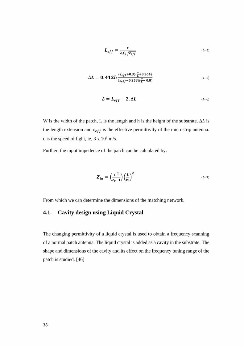
38
𝑳𝒆𝒇𝒇 =𝒄
𝟐.𝒇𝟎√𝜺𝒆𝒇𝒇 (4- 4)
∆𝑳 = 𝟎. 𝟒𝟏𝟐𝒉(𝜺𝒆𝒇𝒇+𝟎.𝟑)(
𝒘
𝒉+𝟎.𝟐𝟔𝟒)
(𝜺𝒆𝒇𝒇−𝟎.𝟐𝟓𝟖)(𝒘
𝒉+ 𝟎.𝟖)
(4- 5)
𝑳 = 𝑳𝒆𝒇𝒇 − 𝟐. ∆𝑳 (4- 6)
W is the width of the patch, L is the length and h is the height of the substrate. ∆𝐿 is
the length extension and 𝜀𝑒𝑓𝑓 is the effective permittivity of the microstrip antenna.
c is the speed of light, ie, 3 x 10⁸ m/s.
Further, the input impedence of the patch can be calculated by:
𝒁𝒊𝒏 = (𝜺𝒓
𝟐
𝜺𝒓−𝟏) (
𝑳
𝑾)
𝟐
(4- 7)
From which we can determine the dimensions of the matching network.
4.1. Cavity design using Liquid Crystal
The changing permittivity of a liquid crystal is used to obtain a frequency scanning
of a normal patch antenna. The liquid crystal is added as a cavity in the substrate. The
shape and dimensions of the cavity and its effect on the frequency tuning range of the
patch is studied. [46]
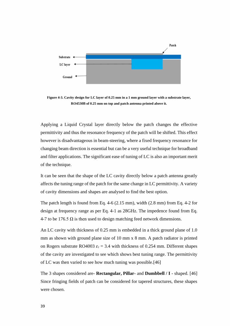
39
Figure 4-3. Cavity design for LC layer of 0.25 mm in a 1 mm ground layer with a substrate layer,
RO4530B of 0.25 mm on top and patch antenna printed above it.
Applying a Liquid Crystal layer directly below the patch changes the effective
permittivity and thus the resonance frequency of the patch will be shifted. This effect
however is disadvantageous in beam-steering, where a fixed frequency resonance for
changing beam direction is essential but can be a very useful technique for broadband
and filter applications. The significant ease of tuning of LC is also an important merit
of the technique.
It can be seen that the shape of the LC cavity directly below a patch antenna greatly
affects the tuning range of the patch for the same change in LC permittivity. A variety
of cavity dimensions and shapes are analysed to find the best option.
The patch length is found from Eq. 4-6 (2.15 mm), width (2.8 mm) from Eq. 4-2 for
design at frequency range as per Eq. 4-1 as 28GHz. The impedence found from Eq.
4-7 to be 176.5 Ω is then used to design matching feed network dimensions.
An LC cavity with thickness of 0.25 mm is embedded in a thick ground plane of 1.0
mm as shown with ground plane size of 10 mm x 8 mm. A patch radiator is printed
on Rogers substrate RO4003 𝜀r = 3.4 with thickness of 0.254 mm. Different shapes
of the cavity are investigated to see which shows best tuning range. The permittivity
of LC was then varied to see how much tuning was possible.[46]
The 3 shapes considered are- Rectangular, Pillar- and Dumbbell / I - shaped. [46]
Since fringing fields of patch can be considered for tapered structures, these shapes
were chosen.
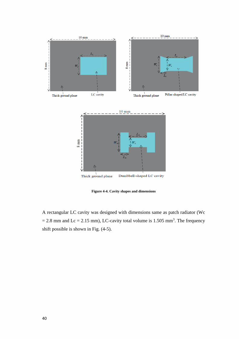
40
Figure 4-4. Cavity shapes and dimensions
A rectangular LC cavity was designed with dimensions same as patch radiator (Wc
= 2.8 mm and Lc = 2.15 mm), LC-cavity total volume is 1.505 mm3. The frequency
shift possible is shown in Fig. (4-5).
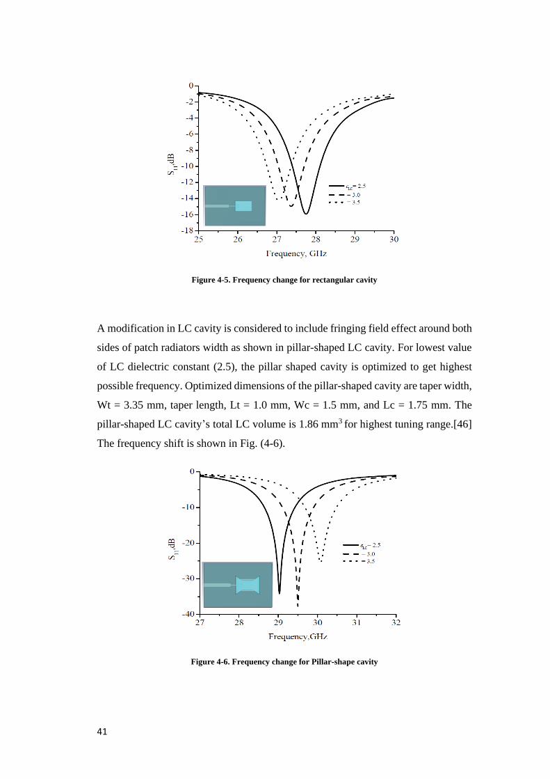
41
Figure 4-5. Frequency change for rectangular cavity
A modification in LC cavity is considered to include fringing field effect around both
sides of patch radiators width as shown in pillar-shaped LC cavity. For lowest value
of LC dielectric constant (2.5), the pillar shaped cavity is optimized to get highest
possible frequency. Optimized dimensions of the pillar-shaped cavity are taper width,
Wt = 3.35 mm, taper length, Lt = 1.0 mm, Wc = 1.5 mm, and Lc = 1.75 mm. The
pillar-shaped LC cavity’s total LC volume is 1.86 mm3 for highest tuning range.[46]
The frequency shift is shown in Fig. (4-6).
Figure 4-6. Frequency change for Pillar-shape cavity
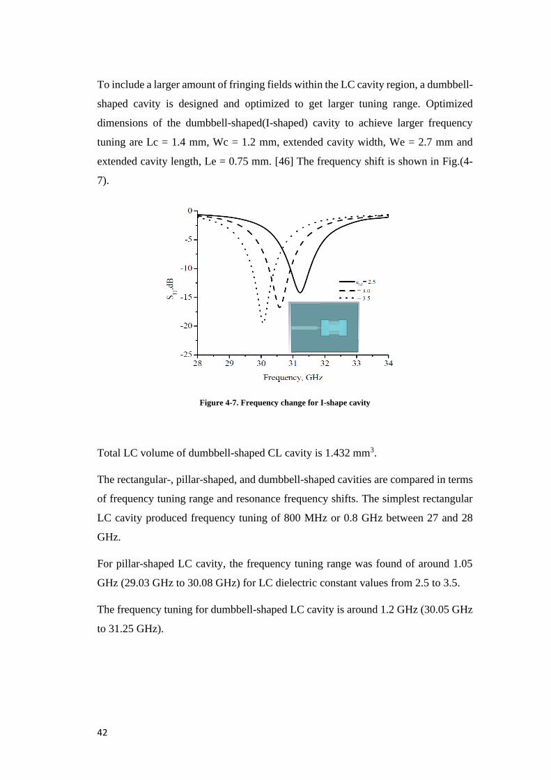
42
To include a larger amount of fringing fields within the LC cavity region, a dumbbell-
shaped cavity is designed and optimized to get larger tuning range. Optimized
dimensions of the dumbbell-shaped(I-shaped) cavity to achieve larger frequency
tuning are Lc = 1.4 mm, Wc = 1.2 mm, extended cavity width, We = 2.7 mm and
extended cavity length, Le = 0.75 mm. [46] The frequency shift is shown in Fig.(4-
7).
Figure 4-7. Frequency change for I-shape cavity
Total LC volume of dumbbell-shaped CL cavity is 1.432 mm3.
The rectangular-, pillar-shaped, and dumbbell-shaped cavities are compared in terms
of frequency tuning range and resonance frequency shifts. The simplest rectangular
LC cavity produced frequency tuning of 800 MHz or 0.8 GHz between 27 and 28
GHz.
For pillar-shaped LC cavity, the frequency tuning range was found of around 1.05
GHz (29.03 GHz to 30.08 GHz) for LC dielectric constant values from 2.5 to 3.5.
The frequency tuning for dumbbell-shaped LC cavity is around 1.2 GHz (30.05 GHz
to 31.25 GHz).
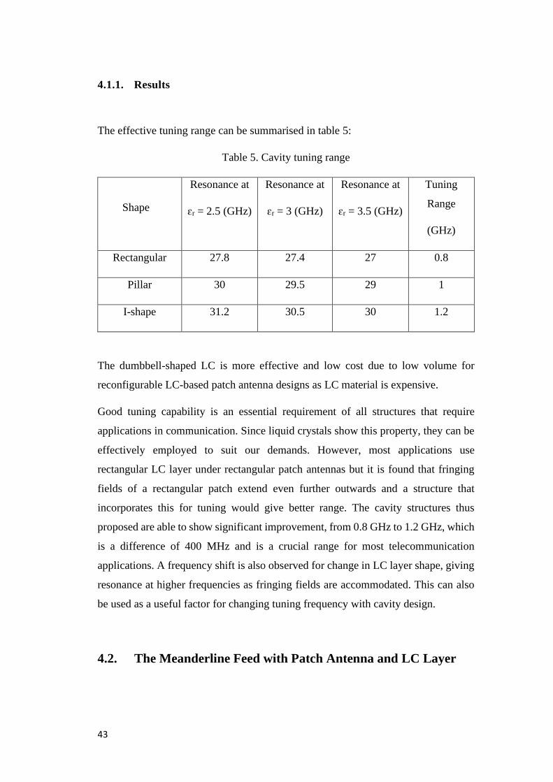
43
4.1.1. Results
The effective tuning range can be summarised in table 5:
Table 5. Cavity tuning range
Shape
Resonance at
ɛr = 2.5 (GHz)
Resonance at
ɛr = 3 (GHz)
Resonance at
ɛr = 3.5 (GHz)
Tuning
Range
(GHz)
Rectangular 27.8 27.4 27 0.8
Pillar 30 29.5 29 1
I-shape 31.2 30.5 30 1.2
The dumbbell-shaped LC is more effective and low cost due to low volume for
reconfigurable LC-based patch antenna designs as LC material is expensive.
Good tuning capability is an essential requirement of all structures that require
applications in communication. Since liquid crystals show this property, they can be
effectively employed to suit our demands. However, most applications use
rectangular LC layer under rectangular patch antennas but it is found that fringing
fields of a rectangular patch extend even further outwards and a structure that
incorporates this for tuning would give better range. The cavity structures thus
proposed are able to show significant improvement, from 0.8 GHz to 1.2 GHz, which
is a difference of 400 MHz and is a crucial range for most telecommunication
applications. A frequency shift is also observed for change in LC layer shape, giving
resonance at higher frequencies as fringing fields are accommodated. This can also
be used as a useful factor for changing tuning frequency with cavity design.
4.2. The Meanderline Feed with Patch Antenna and LC Layer
44
As was seen with the meanderline feed and LC layer design, it showed good phase
shift capability by changing the permittivity of the LC layer.
Commercially available Liquid crystals that can operate at high frequencies like 5CB,
GT3-2001 shows permittivity between 1.5 (𝜀⊥) and 3.9 ( 𝜀//), with loss tangents from
0.004 to 0.03.
For this application, a new material was defined as LC with a loss tangent of 0.02 and
permittivity changing from 2.5 to 3.5, which is a range that is practically achievable
with DC voltages below 5V.
4.2.1. 1 x 4 Array
The meanderline feed and LC layer was then applied as part of feeding network to
the rectangular 1 x 4 patch antenna array.
The variation of each LC layer’s permittivity in the array will cause different phase
shifts at each patch, thereby causing main beam formed by the array to change
direction depending on the combination of phase shifts applied.
The structure consists of 2 layers- a ROGERS RO4350B substrate of 0.813 mm
thickness with a 0.508 mm thick ground plane of PEC below it. The meanderline feed
with LC layer of 0.258 mm is then embedded inside the thick ground plane. The patch
antenna and matching network is on the top of the substrate and is connected to the
meanderline feed below substrate using vias.
The meanderline feed was made below the main layer since meanderline also acts as
an antenna and radiates along the longer edges of the meander. This can interfere with
the patch antenna radiation, and this is one method to subdue the strength of the
radiation caused by meanderline.
The patch antenna was designed to operate/resonate at 28 GHz with W=2.4 mm and
L= 2.75 mm with thickness of 0.017 mm. The antenna’s impedence of 176 ꭥ needed
to be matched to 0.11 mm microstrip line feed and a small inset was made to achieve
this. The inset length was 0.5 mm and width of 0.2 mm on both sides of feed. It was
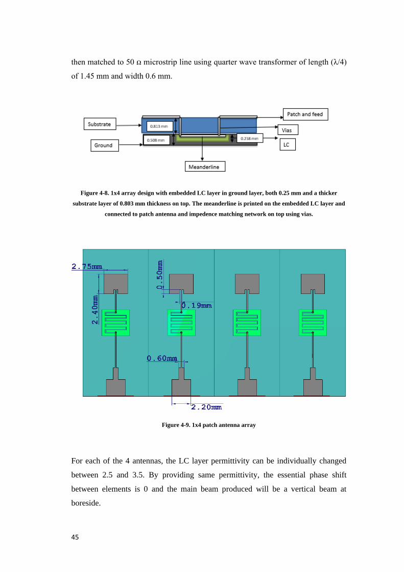
45
then matched to 50 ꭥ microstrip line using quarter wave transformer of length (λ/4)
of 1.45 mm and width 0.6 mm.
Figure 4-8. 1x4 array design with embedded LC layer in ground layer, both 0.25 mm and a thicker
substrate layer of 0.803 mm thickness on top. The meanderline is printed on the embedded LC layer and
connected to patch antenna and impedence matching network on top using vias.
Figure 4-9. 1x4 patch antenna array
For each of the 4 antennas, the LC layer permittivity can be individually changed
between 2.5 and 3.5. By providing same permittivity, the essential phase shift
between elements is 0 and the main beam produced will be a vertical beam at
boreside.
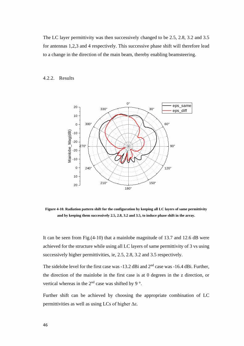
46
The LC layer permittivity was then successively changed to be 2.5, 2.8, 3.2 and 3.5
for antennas 1,2,3 and 4 respectively. This successive phase shift will therefore lead
to a change in the direction of the main beam, thereby enabling beamsteering.
4.2.2. Results
Figure 4-10. Radiation pattern shift for the configuration by keeping all LC layers of same permittivity
and by keeping them successively 2.5, 2.8, 3.2 and 3.5, to induce phase shift in the array.
It can be seen from Fig.(4-10) that a mainlobe magnitude of 13.7 and 12.6 dB were
achieved for the structure while using all LC layers of same permittivity of 3 vs using
successively higher permittivities, ie, 2.5, 2.8, 3.2 and 3.5 respectively.
The sidelobe level for the first case was -13.2 dBi and 2nd case was -16.4 dBi. Further,
the direction of the mainlobe in the first case is at 0 degrees in the z direction, or
vertical whereas in the 2nd case was shifted by 9 °.
Further shift can be achieved by choosing the appropriate combination of LC
permittivities as well as using LCs of higher Δε.
0°
30°
60°
90°
120°
150°
180°
210°
240°
270°
300°
330°
-20
-10
0
10
20
-20
-10
0
10
20
Main
lob
e_
Ma
g(d
B)
eps_same
eps_diff
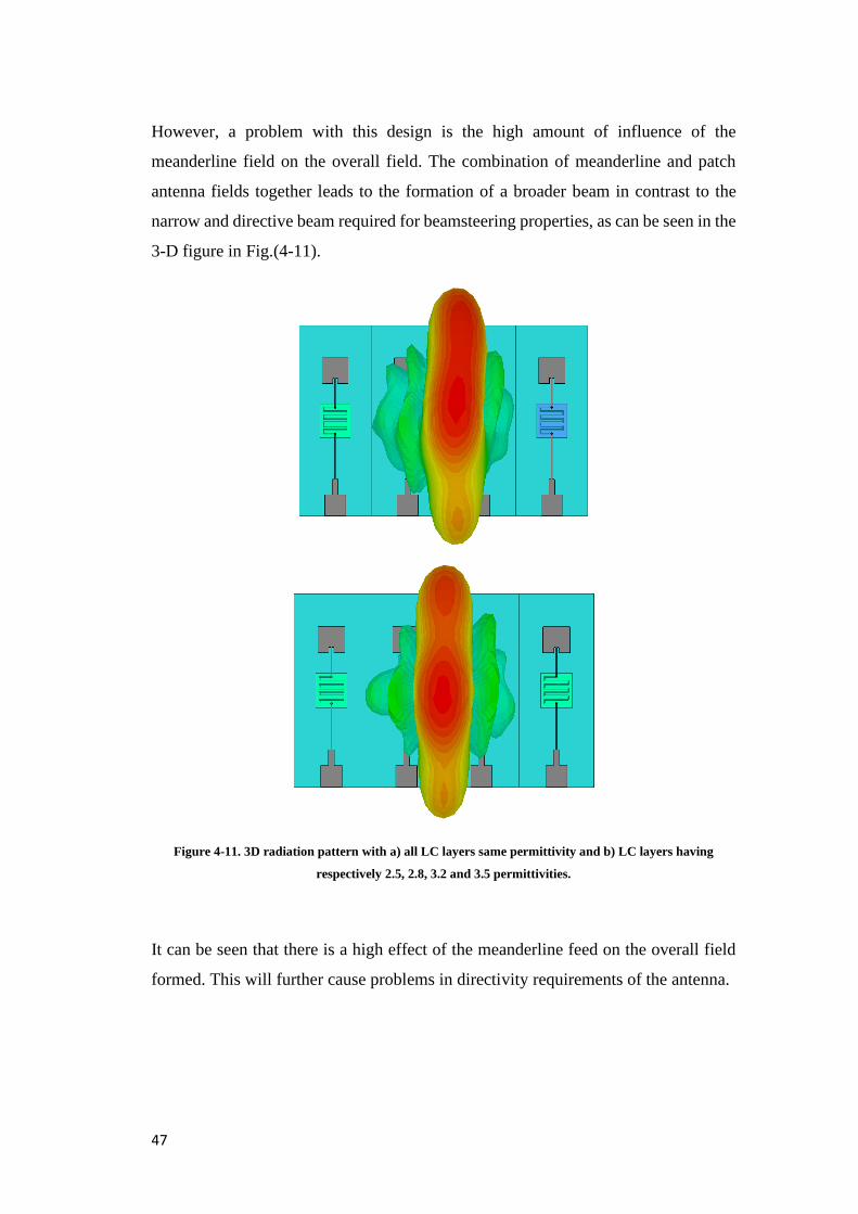
47
However, a problem with this design is the high amount of influence of the
meanderline field on the overall field. The combination of meanderline and patch
antenna fields together leads to the formation of a broader beam in contrast to the
narrow and directive beam required for beamsteering properties, as can be seen in the
3-D figure in Fig.(4-11).
Figure 4-11. 3D radiation pattern with a) all LC layers same permittivity and b) LC layers having
respectively 2.5, 2.8, 3.2 and 3.5 permittivities.
It can be seen that there is a high effect of the meanderline feed on the overall field
formed. This will further cause problems in directivity requirements of the antenna.
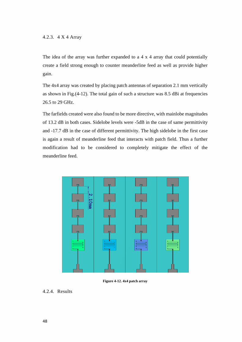
48
4.2.3. 4 X 4 Array
The idea of the array was further expanded to a 4 x 4 array that could potentially
create a field strong enough to counter meanderline feed as well as provide higher
gain.
The 4x4 array was created by placing patch antennas of separation 2.1 mm vertically
as shown in Fig.(4-12). The total gain of such a structure was 8.5 dBi at frequencies
26.5 to 29 GHz.
The farfields created were also found to be more directive, with mainlobe magnitudes
of 13.2 dB in both cases. Sidelobe levels were -5dB in the case of same permittivity
and -17.7 dB in the case of different permittivity. The high sidelobe in the first case
is again a result of meanderline feed that interacts with patch field. Thus a further
modification had to be considered to completely mitigate the effect of the
meanderline feed.
Figure 4-12. 4x4 patch array
4.2.4. Results
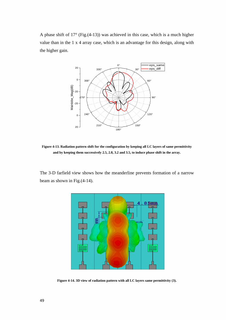
49
A phase shift of 17° (Fig.(4-13)) was achieved in this case, which is a much higher
value than in the 1 x 4 array case, which is an advantage for this design, along with
the higher gain.
Figure 4-13. Radiation pattern shift for the configuration by keeping all LC layers of same permittivity
and by keeping them successively 2.5, 2.8, 3.2 and 3.5, to induce phase shift in the array.
The 3-D farfield view shows how the meanderline prevents formation of a narrow
beam as shown in Fig.(4-14).
Figure 4-14. 3D view of radiation pattern with all LC layers same permittivity (3).
0°
30°
60°
90°
120°
150°
180°
210°
240°
270°
300°
330°
-20
0
20
-20
0
20
Main
lob
e_
Ma
g(d
B)
eps_same
eps_diff
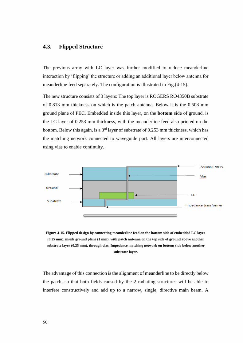
50
4.3. Flipped Structure
The previous array with LC layer was further modified to reduce meanderline
interaction by ‘flipping’ the structure or adding an additional layer below antenna for
meanderline feed separately. The configuration is illustrated in Fig.(4-15).
The new structure consists of 3 layers: The top layer is ROGERS RO4350B substrate
of 0.813 mm thickness on which is the patch antenna. Below it is the 0.508 mm
ground plane of PEC. Embedded inside this layer, on the bottom side of ground, is
the LC layer of 0.253 mm thickness, with the meanderline feed also printed on the
bottom. Below this again, is a 3rd layer of substrate of 0.253 mm thickness, which has
the matching network connected to waveguide port. All layers are interconnected
using vias to enable continuity.
Figure 4-15. Flipped design by connecting meanderline feed on the bottom side of embedded LC layer
(0.25 mm), inside ground plane (1 mm), with patch antenna on the top side of ground above another
substrate layer (0.25 mm), through vias. Impedence matching network on bottom side below another
substrate layer.
The advantage of this connection is the alignment of meanderline to be directly below
the patch, so that both fields caused by the 2 radiating structures will be able to
interfere constructively and add up to a narrow, single, directive main beam. A
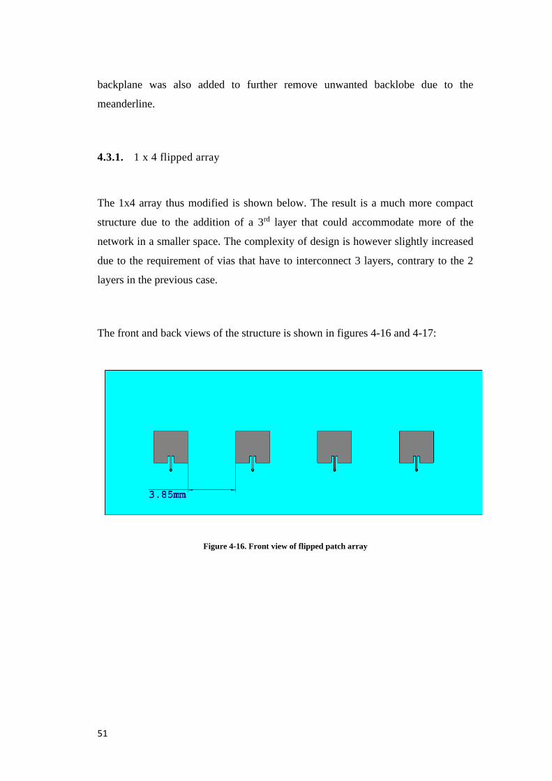
51
backplane was also added to further remove unwanted backlobe due to the
meanderline.
4.3.1. 1 x 4 flipped array
The 1x4 array thus modified is shown below. The result is a much more compact
structure due to the addition of a 3rd layer that could accommodate more of the
network in a smaller space. The complexity of design is however slightly increased
due to the requirement of vias that have to interconnect 3 layers, contrary to the 2
layers in the previous case.
The front and back views of the structure is shown in figures 4-16 and 4-17:
Figure 4-16. Front view of flipped patch array
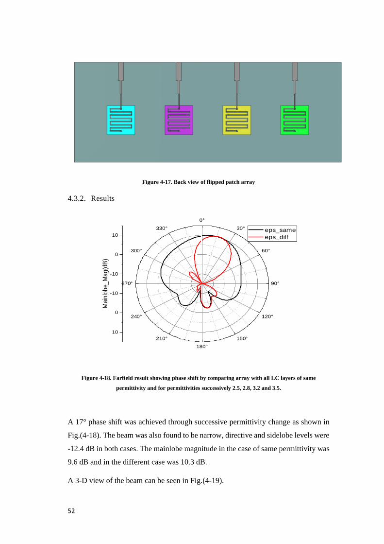
52
Figure 4-17. Back view of flipped patch array
4.3.2. Results
Figure 4-18. Farfield result showing phase shift by comparing array with all LC layers of same
permittivity and for permittivities successively 2.5, 2.8, 3.2 and 3.5.
A 17° phase shift was achieved through successive permittivity change as shown in
Fig.(4-18). The beam was also found to be narrow, directive and sidelobe levels were
-12.4 dB in both cases. The mainlobe magnitude in the case of same permittivity was
9.6 dB and in the different case was 10.3 dB.
A 3-D view of the beam can be seen in Fig.(4-19).
0°
30°
60°
90°
120°
150°
180°
210°
240°
270°
300°
330°
-10
0
10
-10
0
10
Mai
nlo
be_
Ma
g(d
B)
eps_same
eps_diff
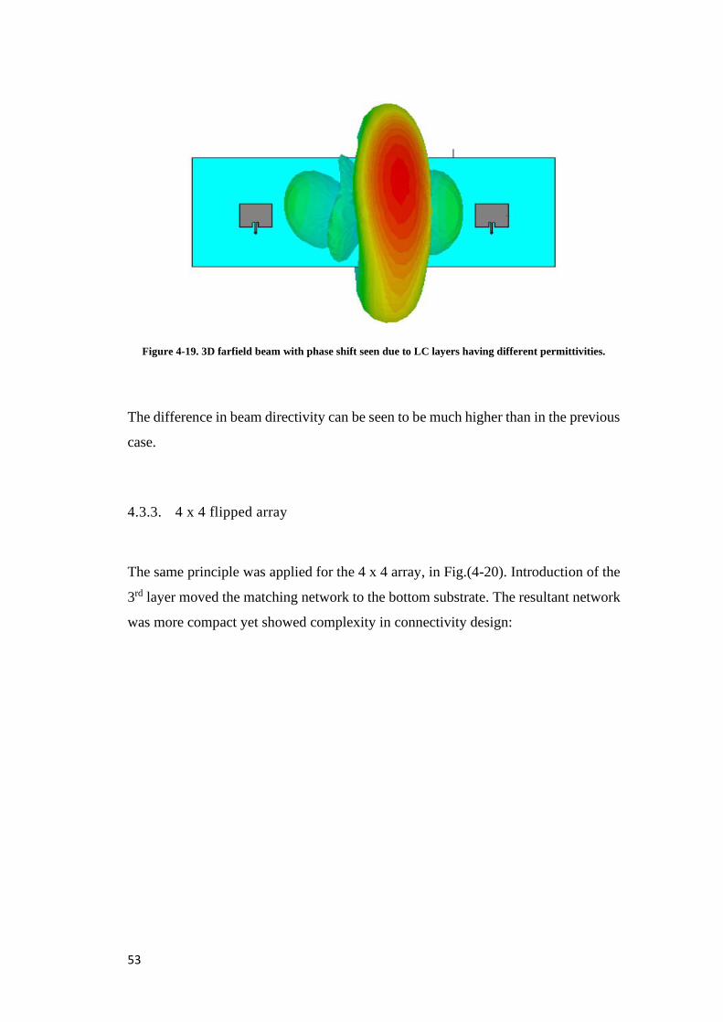
53
Figure 4-19. 3D farfield beam with phase shift seen due to LC layers having different permittivities.
The difference in beam directivity can be seen to be much higher than in the previous
case.
4.3.3. 4 x 4 flipped array
The same principle was applied for the 4 x 4 array, in Fig.(4-20). Introduction of the
3rd layer moved the matching network to the bottom substrate. The resultant network
was more compact yet showed complexity in connectivity design:
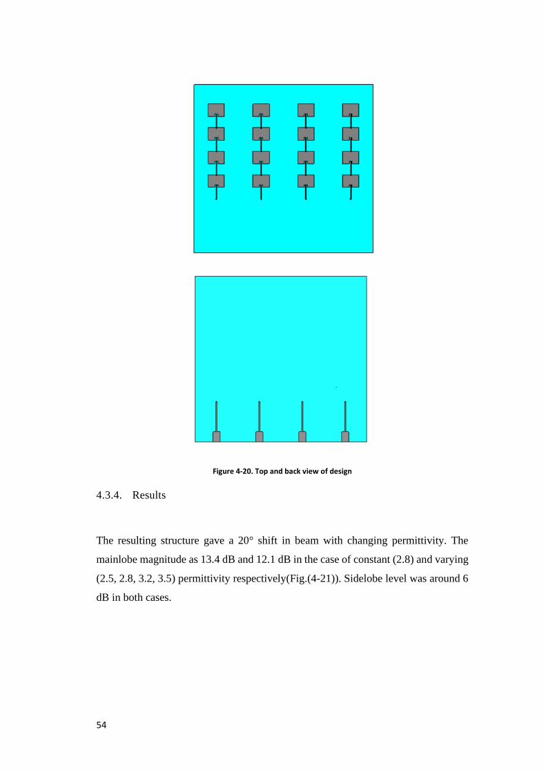
54
Figure 4-20. Top and back view of design
4.3.4. Results
The resulting structure gave a 20° shift in beam with changing permittivity. The
mainlobe magnitude as 13.4 dB and 12.1 dB in the case of constant (2.8) and varying
(2.5, 2.8, 3.2, 3.5) permittivity respectively(Fig.(4-21)). Sidelobe level was around 6
dB in both cases.
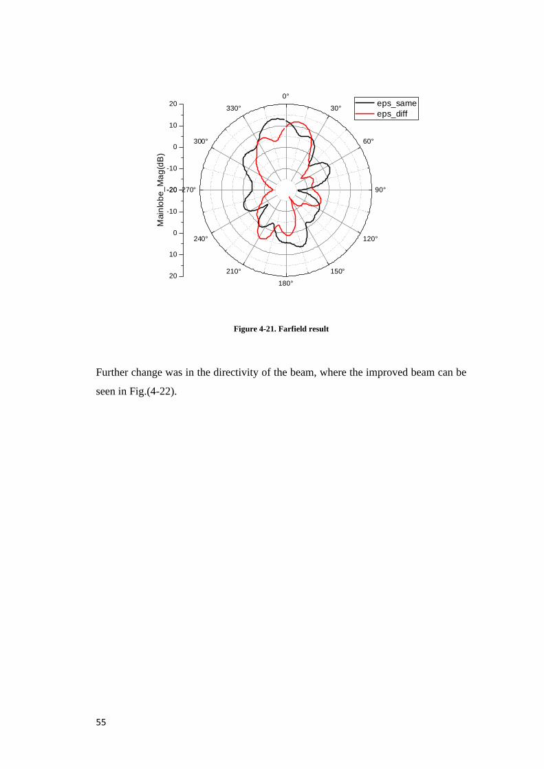
55
Figure 4-21. Farfield result
Further change was in the directivity of the beam, where the improved beam can be
seen in Fig.(4-22).
0°
30°
60°
90°
120°
150°
180°
210°
240°
270°
300°
330°
-20
-10
0
10
20
-20
-10
0
10
20
Main
lob
e_
Ma
g(d
B)
eps_same
eps_diff
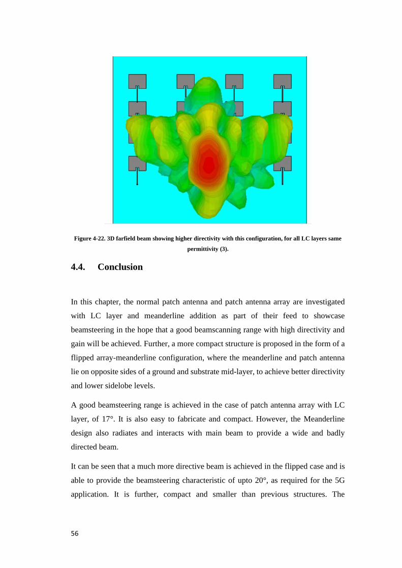
56
Figure 4-22. 3D farfield beam showing higher directivity with this configuration, for all LC layers same
permittivity (3).
4.4. Conclusion
In this chapter, the normal patch antenna and patch antenna array are investigated
with LC layer and meanderline addition as part of their feed to showcase
beamsteering in the hope that a good beamscanning range with high directivity and
gain will be achieved. Further, a more compact structure is proposed in the form of a
flipped array-meanderline configuration, where the meanderline and patch antenna
lie on opposite sides of a ground and substrate mid-layer, to achieve better directivity
and lower sidelobe levels.
A good beamsteering range is achieved in the case of patch antenna array with LC
layer, of 17°. It is also easy to fabricate and compact. However, the Meanderline
design also radiates and interacts with main beam to provide a wide and badly
directed beam.
It can be seen that a much more directive beam is achieved in the flipped case and is
able to provide the beamsteering characteristic of upto 20°, as required for the 5G
application. It is further, compact and smaller than previous structures. The
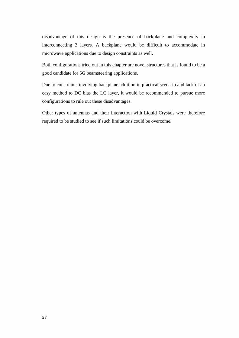
57
disadvantage of this design is the presence of backplane and complexity in
interconnecting 3 layers. A backplane would be difficult to accommodate in
microwave applications due to design constraints as well.
Both configurations tried out in this chapter are novel structures that is found to be a
good candidate for 5G beamsteering applications.
Due to constraints involving backplane addition in practical scenario and lack of an
easy method to DC bias the LC layer, it would be recommended to pursue more
configurations to rule out these disadvantages.
Other types of antennas and their interaction with Liquid Crystals were therefore
required to be studied to see if such limitations could be overcome.
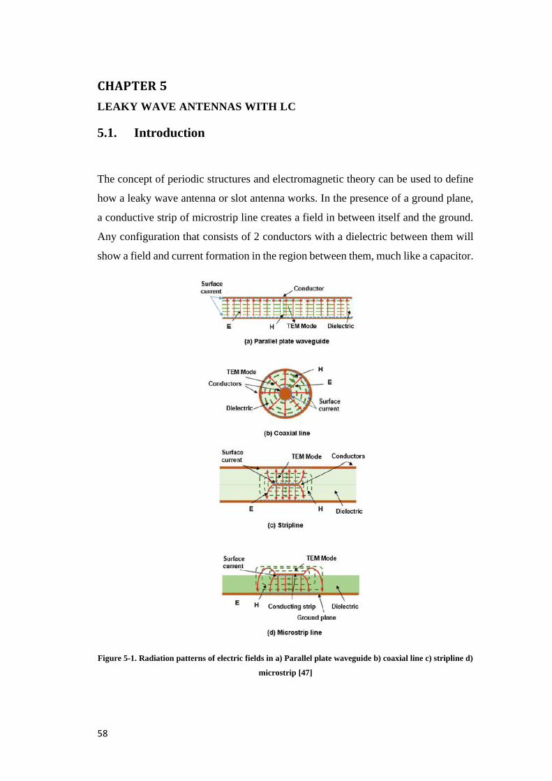
58
CHAPTER 5
LEAKY WAVE ANTENNAS WITH LC
5.1. Introduction
The concept of periodic structures and electromagnetic theory can be used to define
how a leaky wave antenna or slot antenna works. In the presence of a ground plane,
a conductive strip of microstrip line creates a field in between itself and the ground.
Any configuration that consists of 2 conductors with a dielectric between them will
show a field and current formation in the region between them, much like a capacitor.
Figure 5-1. Radiation patterns of electric fields in a) Parallel plate waveguide b) coaxial line c) stripline d)
microstrip [47]
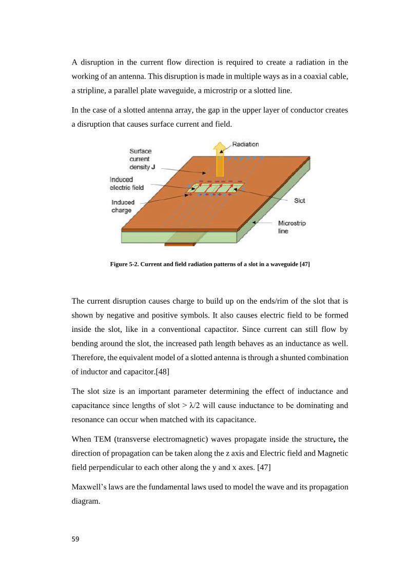
59
A disruption in the current flow direction is required to create a radiation in the
working of an antenna. This disruption is made in multiple ways as in a coaxial cable,
a stripline, a parallel plate waveguide, a microstrip or a slotted line.
In the case of a slotted antenna array, the gap in the upper layer of conductor creates
a disruption that causes surface current and field.
Figure 5-2. Current and field radiation patterns of a slot in a waveguide [47]
The current disruption causes charge to build up on the ends/rim of the slot that is
shown by negative and positive symbols. It also causes electric field to be formed
inside the slot, like in a conventional capactitor. Since current can still flow by
bending around the slot, the increased path length behaves as an inductance as well.
Therefore, the equivalent model of a slotted antenna is through a shunted combination
of inductor and capacitor.[48]
The slot size is an important parameter determining the effect of inductance and
capacitance since lengths of slot > λ/2 will cause inductance to be dominating and
resonance can occur when matched with its capacitance.
When TEM (transverse electromagnetic) waves propagate inside the structure, the
direction of propagation can be taken along the z axis and Electric field and Magnetic
field perpendicular to each other along the y and x axes. [47]
Maxwell’s laws are the fundamental laws used to model the wave and its propagation
diagram.
60
Using Maxwell’s theorems, the electric (E) and magnetic (H) fields can be modelled
as:[47]
𝐄 = 𝐀𝐬𝐢𝐧(𝐳 − 𝐜𝐭) + 𝐁𝐬𝐢𝐧(𝐳 + 𝐜𝐭)x (5- 1)
𝐇 = 𝐂𝐬𝐢𝐧(𝐳 − 𝐜𝐭) + 𝐃𝐬𝐢𝐧(𝐳 + 𝐜𝐭)y (5- 2)
The ratio of Electric field to Magnetic field will in turn give the impedence of the
structure, called characteristic impdence.
𝐄
𝐇= √
𝛍
𝛆= 𝒛𝟎 (5- 3)
Further, the propagation constant in free space can be defined as k0= ω√𝛆𝛍 (5- 4)
Inside a waveguide or leaky wave structure, the waves tend to form standing waves
and thus the equation will have to be modified slightly.[47]
Figure 5-3. Conventional LWA [47]
The phase velocity of the wave as it travels along the waveguide can be defined as
𝐯𝐩 = 𝐜 𝐬𝐢𝐧𝛉⁄ (5- 5)
where θ is the where θ is the angle made by the electric field vector (E) with the
direction of propagation, or the z axis.
Thus, the phase constant
𝛃𝐩 = 𝐤𝟎𝐬𝐢𝐧𝛉 (5- 6)
The sinusoidal wave variations can be related using the trigonometric equation as
𝐜𝐨𝐬𝛉 = 𝐦𝛌𝟐𝐚⁄ (5- 7)
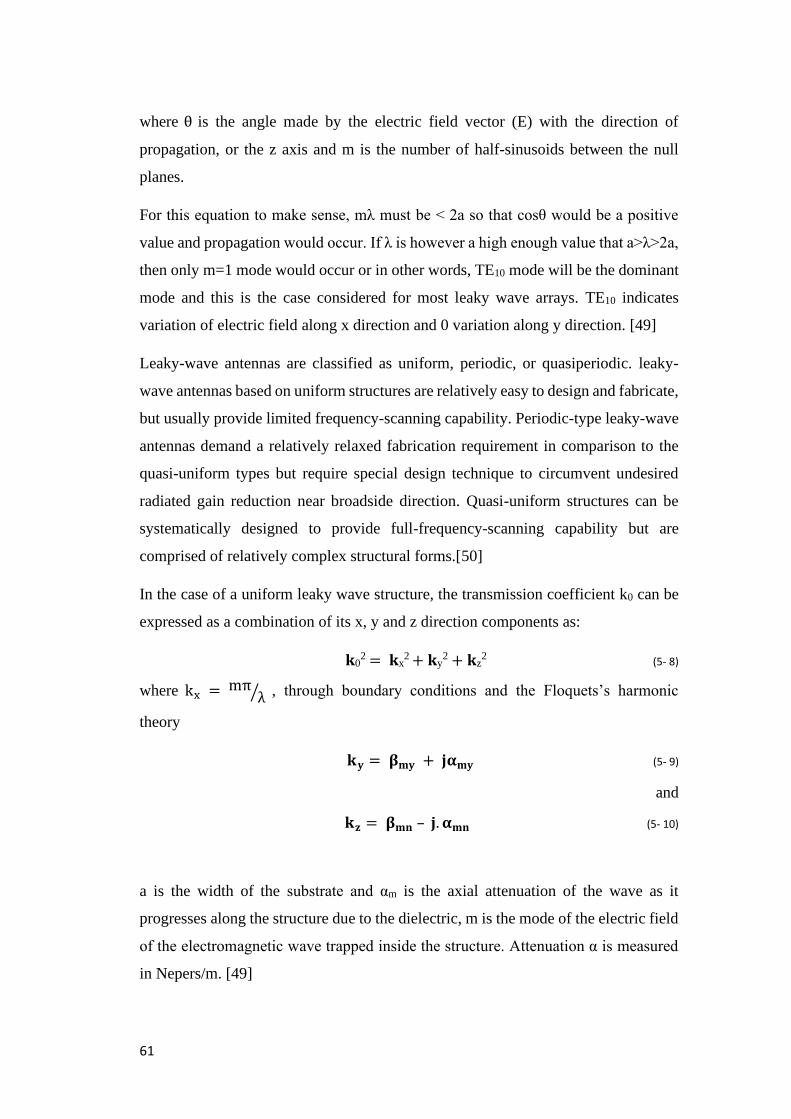
61
where θ is the angle made by the electric field vector (E) with the direction of
propagation, or the z axis and m is the number of half-sinusoids between the null
planes.
For this equation to make sense, mλ must be < 2a so that cosθ would be a positive
value and propagation would occur. If λ is however a high enough value that a>λ>2a,
then only m=1 mode would occur or in other words, TE10 mode will be the dominant
mode and this is the case considered for most leaky wave arrays. TE10 indicates
variation of electric field along x direction and 0 variation along y direction. [49]
Leaky-wave antennas are classified as uniform, periodic, or quasiperiodic. leaky-
wave antennas based on uniform structures are relatively easy to design and fabricate,
but usually provide limited frequency-scanning capability. Periodic-type leaky-wave
antennas demand a relatively relaxed fabrication requirement in comparison to the
quasi-uniform types but require special design technique to circumvent undesired
radiated gain reduction near broadside direction. Quasi-uniform structures can be
systematically designed to provide full-frequency-scanning capability but are
comprised of relatively complex structural forms.[50]
In the case of a uniform leaky wave structure, the transmission coefficient k0 can be
expressed as a combination of its x, y and z direction components as:
𝐤02 = 𝐤x
2 + 𝐤y2 + 𝐤z
2 (5- 8)
where kx = mπλ⁄ , through boundary conditions and the Floquets’s harmonic
theory
𝐤𝐲 = 𝛃𝐦𝐲 + 𝐣𝛂𝐦𝐲 (5- 9)
and
𝐤𝐳 = 𝛃𝐦𝐧 – 𝐣. 𝛂𝐦𝐧 (5- 10)
a is the width of the substrate and αm is the axial attenuation of the wave as it
progresses along the structure due to the dielectric, m is the mode of the electric field
of the electromagnetic wave trapped inside the structure. Attenuation α is measured
in Nepers/m. [49]
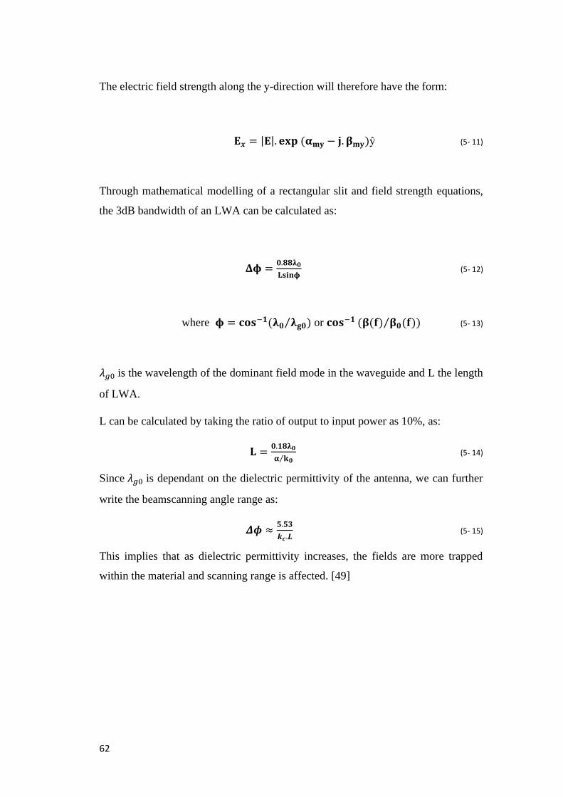
62
The electric field strength along the y-direction will therefore have the form:
𝐄𝒙 = |𝐄|. 𝐞𝐱𝐩 (𝛂𝐦𝐲 − 𝐣. 𝛃𝐦𝐲)y (5- 11)
Through mathematical modelling of a rectangular slit and field strength equations,
the 3dB bandwidth of an LWA can be calculated as:
𝚫𝛟 =𝟎.𝟖𝟖𝛌𝟎
𝐋𝐬𝐢𝐧𝛟 (5- 12)
where 𝛟 = 𝐜𝐨𝐬−𝟏(𝛌𝟎 𝛌𝐠𝟎)⁄ or 𝐜𝐨𝐬−𝟏 (𝛃(𝐟) 𝛃𝟎(𝐟)⁄ ) (5- 13)
𝜆𝑔0 is the wavelength of the dominant field mode in the waveguide and L the length
of LWA.
L can be calculated by taking the ratio of output to input power as 10%, as:
𝐋 =𝟎.𝟏𝟖𝛌𝟎
𝛂 𝐤𝟎⁄ (5- 14)
Since 𝜆𝑔0 is dependant on the dielectric permittivity of the antenna, we can further
write the beamscanning angle range as:
𝜟𝝓 ≈𝟓.𝟓𝟑
𝒌𝒄.𝑳 (5- 15)
This implies that as dielectric permittivity increases, the fields are more trapped
within the material and scanning range is affected. [49]
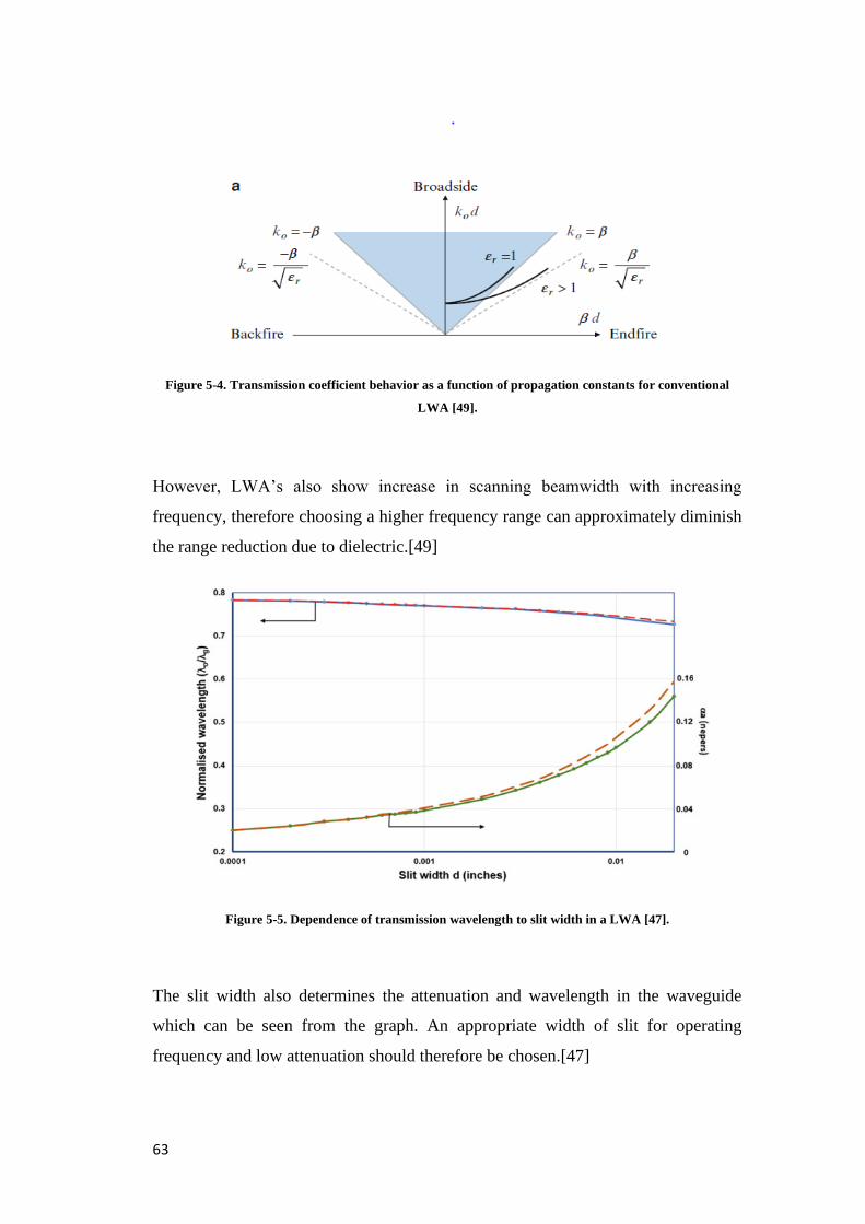
63
Figure 5-4. Transmission coefficient behavior as a function of propagation constants for conventional
LWA [49].
However, LWA’s also show increase in scanning beamwidth with increasing
frequency, therefore choosing a higher frequency range can approximately diminish
the range reduction due to dielectric.[49]
Figure 5-5. Dependence of transmission wavelength to slit width in a LWA [47].
The slit width also determines the attenuation and wavelength in the waveguide
which can be seen from the graph. An appropriate width of slit for operating
frequency and low attenuation should therefore be chosen.[47]
64
Periodic slotted antenna
The transmission coefficient for this case can be written as:
𝐤𝐱𝐧 = √𝐤𝟎𝟐 − 𝛃𝟎
𝟐 (5- 16)
Radiation conditions are satisfied for all nth harmonics located inside it.[47]
Figure 5-6. Transmission coefficient vs propagation constant enhancement using design techniques [49]
This design also gives rise to very large scanning range, between -90° and +90°.
When deciding the distance between slots of a slotted antenna, it can be seen that a
distance of d<λ/2 is recommended so as to allow coupling between consecutive slots
and remove grating lobes. [49]
5.2. Design of circular LWA
The concept of a conventional leaky wave array is combined with a Liquid Crystal
layer design to give rise to a circular LWA with steerable beam.
The design of the circular leaky wave antenna is done such that:
1. The overall diameter of the circle is decided depending on required frequency
of radiation, in this case for 28 GHz, the diameter of 4 mm is chosen. The slit
width is calculated to be 0.5 mm from Fig.(5-5).
2. The circular slot is made inside the circular patch depending on the required
S11 magnitude we assume for the frequency range considered by substituting
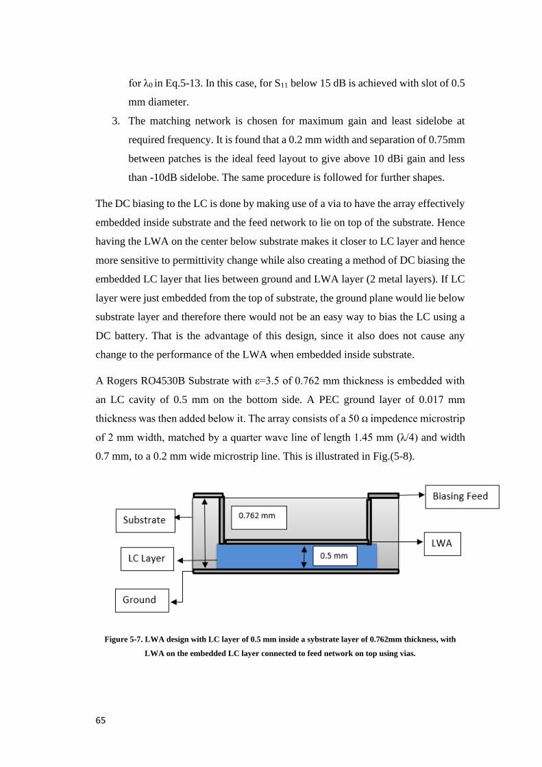
65
for λ0 in Eq.5-13. In this case, for S11 below 15 dB is achieved with slot of 0.5
mm diameter.
3. The matching network is chosen for maximum gain and least sidelobe at
required frequency. It is found that a 0.2 mm width and separation of 0.75mm
between patches is the ideal feed layout to give above 10 dBi gain and less
than -10dB sidelobe. The same procedure is followed for further shapes.
The DC biasing to the LC is done by making use of a via to have the array effectively
embedded inside substrate and the feed network to lie on top of the substrate. Hence
having the LWA on the center below substrate makes it closer to LC layer and hence
more sensitive to permittivity change while also creating a method of DC biasing the
embedded LC layer that lies between ground and LWA layer (2 metal layers). If LC
layer were just embedded from the top of substrate, the ground plane would lie below
substrate layer and therefore there would not be an easy way to bias the LC using a
DC battery. That is the advantage of this design, since it also does not cause any
change to the performance of the LWA when embedded inside substrate.
A Rogers RO4530B Substrate with ε=3.5 of 0.762 mm thickness is embedded with
an LC cavity of 0.5 mm on the bottom side. A PEC ground layer of 0.017 mm
thickness was then added below it. The array consists of a 50 ꭥ impedence microstrip
of 2 mm width, matched by a quarter wave line of length 1.45 mm (λ/4) and width
0.7 mm, to a 0.2 mm wide microstrip line. This is illustrated in Fig.(5-8).
Figure 5-7. LWA design with LC layer of 0.5 mm inside a sybstrate layer of 0.762mm thickness, with
LWA on the embedded LC layer connected to feed network on top using vias.
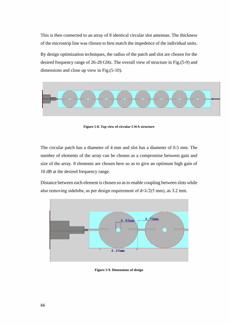
66
This is then connected to an array of 8 identical circular slot antennas. The thickness
of the microstrip line was chosen to best match the impedence of the individual units.
By design optimization techniques, the radius of the patch and slot are chosen for the
desired frequency range of 26-28 GHz. The overall view of structure in Fig.(5-9) and
dimensions and close up view in Fig.(5-10).
Figure 5-8. Top view of circular LWA structure
The circular patch has a diameter of 4 mm and slot has a diameter of 0.5 mm. The
number of elements of the array can be chosen as a compromise between gain and
size of the array. 8 elements are chosen here so as to give an optimum high gain of
10 dB at the desired frequency range.
Distance between each element is chosen so as to enable coupling between slots while
also removing sidelobe, as per design requirement of d<λ/2(5 mm), as 3.2 mm.
Figure 5-9. Dimensions of design
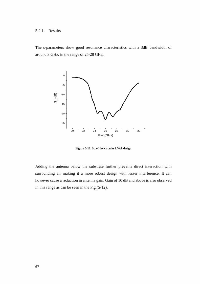
67
5.2.1. Results
The s-parameters show good resonance characteristics with a 3dB bandwidth of
around 3 GHz, in the range of 25-28 GHz.
Figure 5-10. S11 of the circular LWA design
Adding the antenna below the substrate further prevents direct interaction with
surrounding air making it a more robust design with lesser interference. It can
however cause a reduction in antenna gain. Gain of 10 dB and above is also observed
in this range as can be seen in the Fig.(5-12).
20 22 24 26 28 30 32
-25
-20
-15
-10
-5
0
S1
1(d
B)
Freq(GHz)
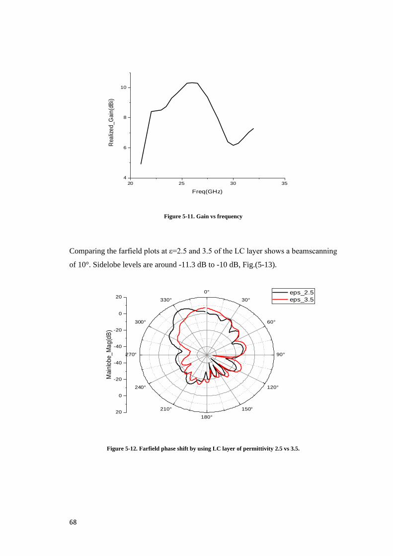
68
Figure 5-11. Gain vs frequency
Comparing the farfield plots at ε=2.5 and 3.5 of the LC layer shows a beamscanning
of 10°. Sidelobe levels are around -11.3 dB to -10 dB, Fig.(5-13).
Figure 5-12. Farfield phase shift by using LC layer of permittivity 2.5 vs 3.5.
20 25 30 35
4
6
8
10
Rea
lize
d_G
ain
(dB
i)
Freq(GHz)
0°
30°
60°
90°
120°
150°
180°
210°
240°
270°
300°
330°
-40
-20
0
20
-40
-20
0
20
Mai
nlo
be_
Ma
g(d
B)
eps_2.5
eps_3.5
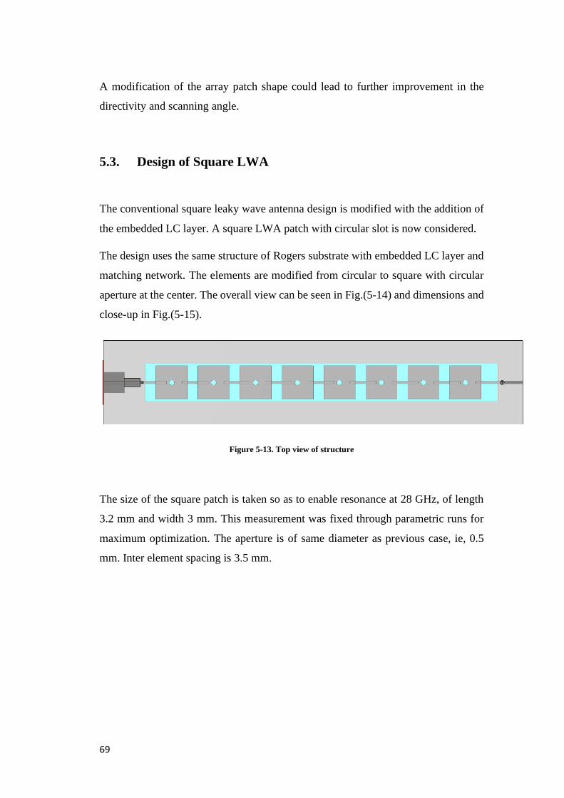
69
A modification of the array patch shape could lead to further improvement in the
directivity and scanning angle.
5.3. Design of Square LWA
The conventional square leaky wave antenna design is modified with the addition of
the embedded LC layer. A square LWA patch with circular slot is now considered.
The design uses the same structure of Rogers substrate with embedded LC layer and
matching network. The elements are modified from circular to square with circular
aperture at the center. The overall view can be seen in Fig.(5-14) and dimensions and
close-up in Fig.(5-15).
Figure 5-13. Top view of structure
The size of the square patch is taken so as to enable resonance at 28 GHz, of length
3.2 mm and width 3 mm. This measurement was fixed through parametric runs for
maximum optimization. The aperture is of same diameter as previous case, ie, 0.5
mm. Inter element spacing is 3.5 mm.
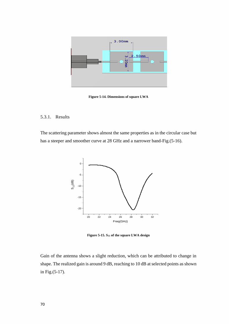
70
Figure 5-14. Dimensions of square LWA
5.3.1. Results
The scattering parameter shows almost the same properties as in the circular case but
has a steeper and smoother curve at 28 GHz and a narrower band-Fig.(5-16).
Figure 5-15. S11 of the square LWA design
Gain of the antenna shows a slight reduction, which can be attributed to change in
shape. The realized gain is around 9 dB, reaching to 10 dB at selected points as shown
in Fig.(5-17).
20 22 24 26 28 30 32
-20
-15
-10
-5
0
S1
1(d
B)
Freq(GHz)
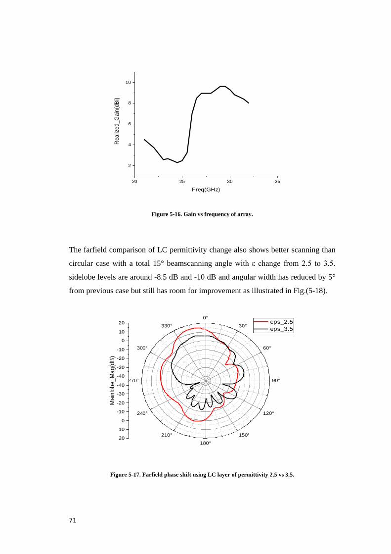
71
Figure 5-16. Gain vs frequency of array.
The farfield comparison of LC permittivity change also shows better scanning than
circular case with a total 15° beamscanning angle with ε change from 2.5 to 3.5.
sidelobe levels are around -8.5 dB and -10 dB and angular width has reduced by 5°
from previous case but still has room for improvement as illustrated in Fig.(5-18).
Figure 5-17. Farfield phase shift using LC layer of permittivity 2.5 vs 3.5.
20 25 30 35
2
4
6
8
10
Rea
lize
d_G
ain
(dB
i)
Freq(GHz)
0°
30°
60°
90°
120°
150°
180°
210°
240°
270°
300°
330°
-40
-30
-20
-10
0
10
20
-40
-30
-20
-10
0
10
20
Main
lob
e_
Ma
g(d
B)
eps_2.5
eps_3.5
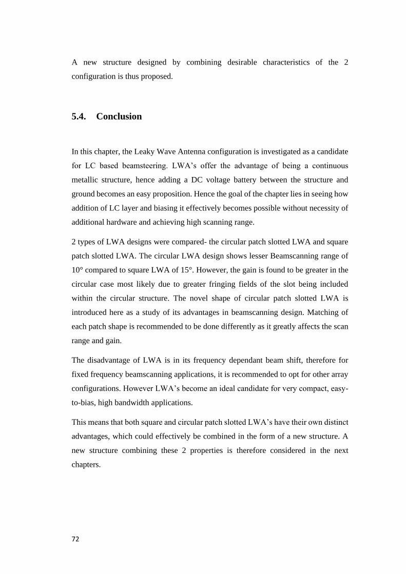
72
A new structure designed by combining desirable characteristics of the 2
configuration is thus proposed.
5.4. Conclusion
In this chapter, the Leaky Wave Antenna configuration is investigated as a candidate
for LC based beamsteering. LWA’s offer the advantage of being a continuous
metallic structure, hence adding a DC voltage battery between the structure and
ground becomes an easy proposition. Hence the goal of the chapter lies in seeing how
addition of LC layer and biasing it effectively becomes possible without necessity of
additional hardware and achieving high scanning range.
2 types of LWA designs were compared- the circular patch slotted LWA and square
patch slotted LWA. The circular LWA design shows lesser Beamscanning range of
10° compared to square LWA of 15°. However, the gain is found to be greater in the
circular case most likely due to greater fringing fields of the slot being included
within the circular structure. The novel shape of circular patch slotted LWA is
introduced here as a study of its advantages in beamscanning design. Matching of
each patch shape is recommended to be done differently as it greatly affects the scan
range and gain.
The disadvantage of LWA is in its frequency dependant beam shift, therefore for
fixed frequency beamscanning applications, it is recommended to opt for other array
configurations. However LWA’s become an ideal candidate for very compact, easy-
to-bias, high bandwidth applications.
This means that both square and circular patch slotted LWA’s have their own distinct
advantages, which could effectively be combined in the form of a new structure. A
new structure combining these 2 properties is therefore considered in the next
chapters.
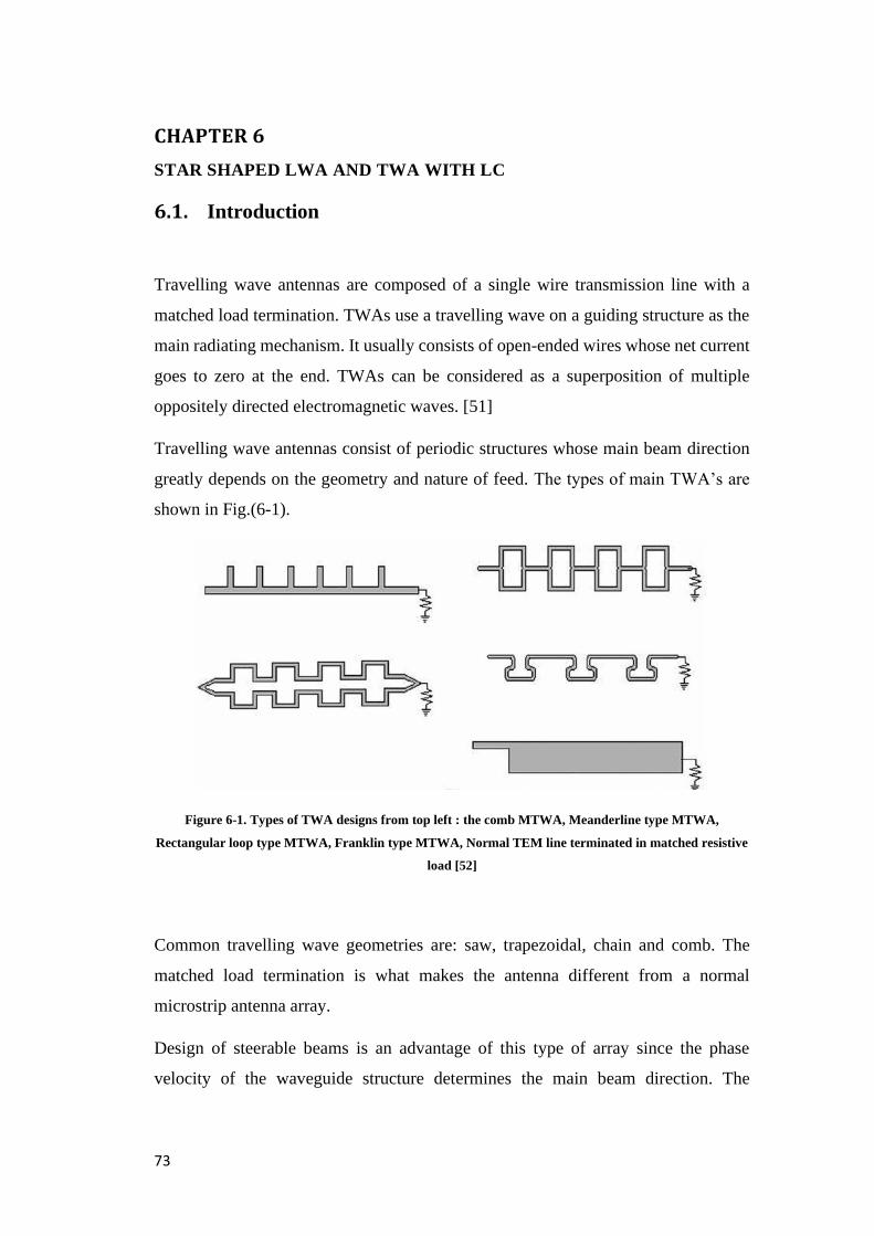
73
CHAPTER 6
STAR SHAPED LWA AND TWA WITH LC
6.1. Introduction
Travelling wave antennas are composed of a single wire transmission line with a
matched load termination. TWAs use a travelling wave on a guiding structure as the
main radiating mechanism. It usually consists of open-ended wires whose net current
goes to zero at the end. TWAs can be considered as a superposition of multiple
oppositely directed electromagnetic waves. [51]
Travelling wave antennas consist of periodic structures whose main beam direction
greatly depends on the geometry and nature of feed. The types of main TWA’s are
shown in Fig.(6-1).
Figure 6-1. Types of TWA designs from top left : the comb MTWA, Meanderline type MTWA,
Rectangular loop type MTWA, Franklin type MTWA, Normal TEM line terminated in matched resistive
load [52]
Common travelling wave geometries are: saw, trapezoidal, chain and comb. The
matched load termination is what makes the antenna different from a normal
microstrip antenna array.
Design of steerable beams is an advantage of this type of array since the phase
velocity of the waveguide structure determines the main beam direction. The
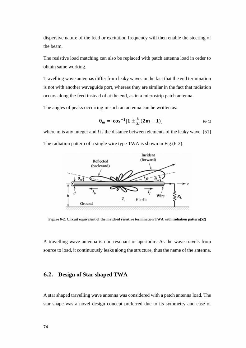
74
dispersive nature of the feed or excitation frequency will then enable the steering of
the beam.
The resistive load matching can also be replaced with patch antenna load in order to
obtain same working.
Travelling wave antennas differ from leaky waves in the fact that the end termination
is not with another waveguide port, whereas they are similar in the fact that radiation
occurs along the feed instead of at the end, as in a microstrip patch antenna.
The angles of peaks occurring in such an antenna can be written as:
𝛉𝐦 = 𝐜𝐨𝐬−𝟏[𝟏 ±𝛌
𝟐𝒍(𝟐𝐦 + 𝟏)] (6- 1)
where m is any integer and l is the distance between elements of the leaky wave. [51]
The radiation pattern of a single wire type TWA is shown in Fig.(6-2).
Figure 6-2. Circuit equivalent of the matched resistive termination TWA with radiation pattern[52]
A travelling wave antenna is non-resonant or aperiodic. As the wave travels from
source to load, it continuously leaks along the structure, thus the name of the antenna.
6.2. Design of Star shaped TWA
A star shaped travelling wave antenna was considered with a patch antenna load. The
star shape was a novel design concept preferred due to its symmetry and ease of
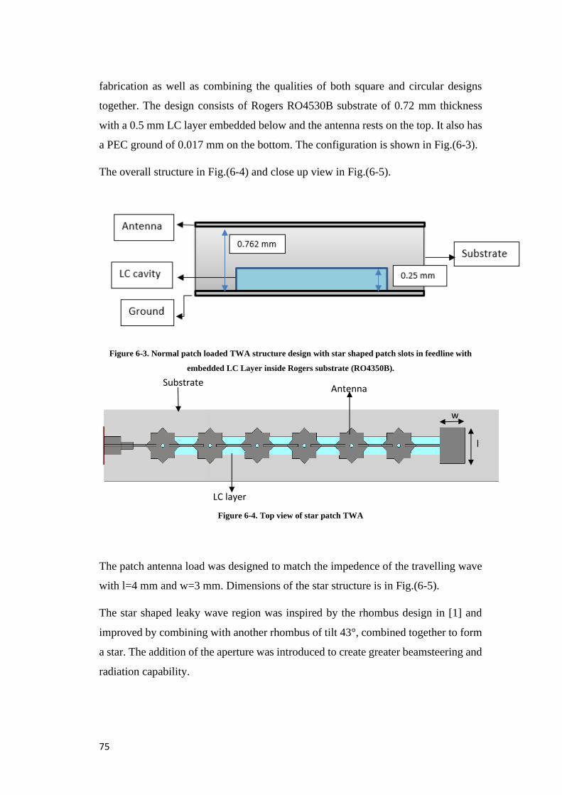
75
fabrication as well as combining the qualities of both square and circular designs
together. The design consists of Rogers RO4530B substrate of 0.72 mm thickness
with a 0.5 mm LC layer embedded below and the antenna rests on the top. It also has
a PEC ground of 0.017 mm on the bottom. The configuration is shown in Fig.(6-3).
The overall structure in Fig.(6-4) and close up view in Fig.(6-5).
Figure 6-3. Normal patch loaded TWA structure design with star shaped patch slots in feedline with
embedded LC Layer inside Rogers substrate (RO4350B).
Figure 6-4. Top view of star patch TWA
The patch antenna load was designed to match the impedence of the travelling wave
with l=4 mm and w=3 mm. Dimensions of the star structure is in Fig.(6-5).
The star shaped leaky wave region was inspired by the rhombus design in [1] and
improved by combining with another rhombus of tilt 43°, combined together to form
a star. The addition of the aperture was introduced to create greater beamsteering and
radiation capability.
l
w
Antenna Substrate
LC layer
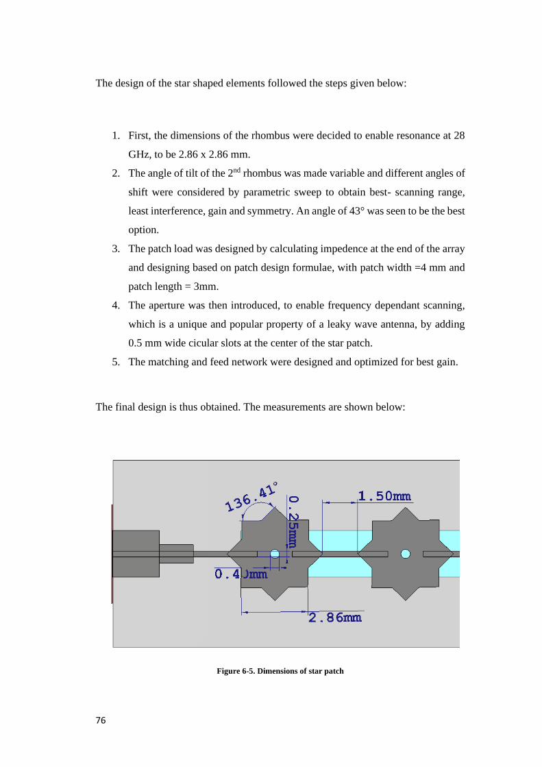
76
The design of the star shaped elements followed the steps given below:
1. First, the dimensions of the rhombus were decided to enable resonance at 28
GHz, to be 2.86 x 2.86 mm.
2. The angle of tilt of the 2nd rhombus was made variable and different angles of
shift were considered by parametric sweep to obtain best- scanning range,
least interference, gain and symmetry. An angle of 43° was seen to be the best
option.
3. The patch load was designed by calculating impedence at the end of the array
and designing based on patch design formulae, with patch width =4 mm and
patch length = 3mm.
4. The aperture was then introduced, to enable frequency dependant scanning,
which is a unique and popular property of a leaky wave antenna, by adding
0.5 mm wide cicular slots at the center of the star patch.
5. The matching and feed network were designed and optimized for best gain.
The final design is thus obtained. The measurements are shown below:
Figure 6-5. Dimensions of star patch
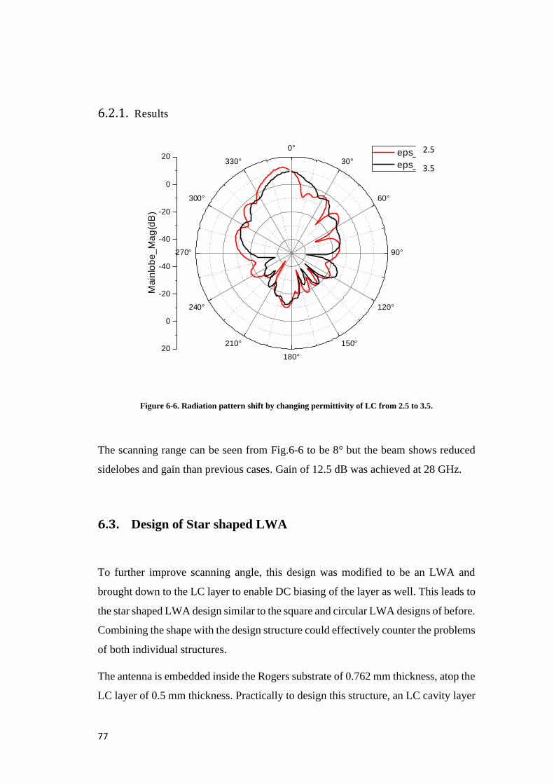
77
6.2.1. Results
Figure 6-6. Radiation pattern shift by changing permittivity of LC from 2.5 to 3.5.
The scanning range can be seen from Fig.6-6 to be 8° but the beam shows reduced
sidelobes and gain than previous cases. Gain of 12.5 dB was achieved at 28 GHz.
6.3. Design of Star shaped LWA
To further improve scanning angle, this design was modified to be an LWA and
brought down to the LC layer to enable DC biasing of the layer as well. This leads to
the star shaped LWA design similar to the square and circular LWA designs of before.
Combining the shape with the design structure could effectively counter the problems
of both individual structures.
The antenna is embedded inside the Rogers substrate of 0.762 mm thickness, atop the
LC layer of 0.5 mm thickness. Practically to design this structure, an LC cavity layer
0°
30°
60°
90°
120°
150°
180°
210°
240°
270°
300°
330°
-40
-20
0
20
-40
-20
0
20
Main
lob
e_
Ma
g(d
B)
eps_diff
eps_same
2.5
3.5
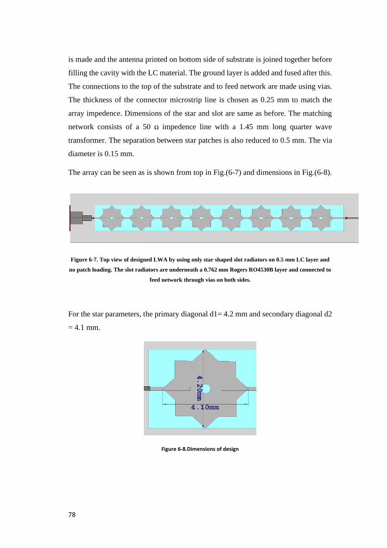
78
is made and the antenna printed on bottom side of substrate is joined together before
filling the cavity with the LC material. The ground layer is added and fused after this.
The connections to the top of the substrate and to feed network are made using vias.
The thickness of the connector microstrip line is chosen as 0.25 mm to match the
array impedence. Dimensions of the star and slot are same as before. The matching
network consists of a 50 ꭥ impedence line with a 1.45 mm long quarter wave
transformer. The separation between star patches is also reduced to 0.5 mm. The via
diameter is 0.15 mm.
The array can be seen as is shown from top in Fig.(6-7) and dimensions in Fig.(6-8).
Figure 6-7. Top view of designed LWA by using only star shaped slot radiators on 0.5 mm LC layer and
no patch loading. The slot radiators are underneath a 0.762 mm Rogers RO4530B layer and connected to
feed network through vias on both sides.
For the star parameters, the primary diagonal d1= 4.2 mm and secondary diagonal d2
= 4.1 mm.
Figure 6-8.Dimensions of design
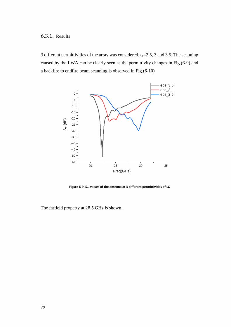
79
6.3.1. Results
3 different permittivities of the array was considered. ɛr=2.5, 3 and 3.5. The scanning
caused by the LWA can be clearly seen as the permittivity changes in Fig.(6-9) and
a backfire to endfire beam scanning is observed in Fig.(6-10).
Figure 6-9. S11 values of the antenna at 3 different permittivities of LC
The farfield property at 28.5 GHz is shown.
20 25 30 35
-55
-50
-45
-40
-35
-30
-25
-20
-15
-10
-5
0
S1
1(d
B)
Freq(GHz)
eps_3.5
eps_3
eps_2.5
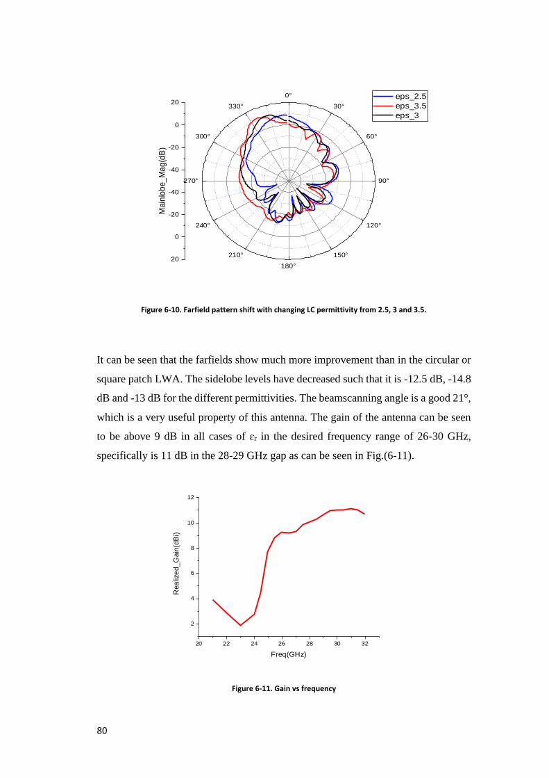
80
Figure 6-10. Farfield pattern shift with changing LC permittivity from 2.5, 3 and 3.5.
It can be seen that the farfields show much more improvement than in the circular or
square patch LWA. The sidelobe levels have decreased such that it is -12.5 dB, -14.8
dB and -13 dB for the different permittivities. The beamscanning angle is a good 21°,
which is a very useful property of this antenna. The gain of the antenna can be seen
to be above 9 dB in all cases of ɛr in the desired frequency range of 26-30 GHz,
specifically is 11 dB in the 28-29 GHz gap as can be seen in Fig.(6-11).
Figure 6-11. Gain vs frequency
0°
30°
60°
90°
120°
150°
180°
210°
240°
270°
300°
330°
-40
-20
0
20
-40
-20
0
20
Main
lob
e_
Ma
g(d
B)
eps_2.5
eps_3.5
eps_3
20 22 24 26 28 30 32
2
4
6
8
10
12
Rea
lize
d_G
ain
(dB
i)
Freq(GHz)
81
6.4. Star shaped array
The configuration above was found to be a useful and efficient structure. Thus, it was
expanded into a 4 x 8 array, to enable massive MIMO and increase overall gain.
This configuration is an efficient, compact and highly directive antenna design
combining the useful properties of a travelling wave antenna as well as a leaky wave
structure. The shape is optimized from previous designs for high gain and directivity.
The overall view in Fig.(6-12).
Figure 6-12. Top view of star LWA array
The 4 separate waveguide ports/feeds provide multiple uses- a) It increases the
number of antennas/patches thereby requiring each antenna to have comparatively
lower gain than in a single line structure, which is the basic use of a MIMO array and
b) Allows separate basing for adjacent array lines, which becomes a very useful
property since each line uses separate LC cavities that can be biased simultaneously
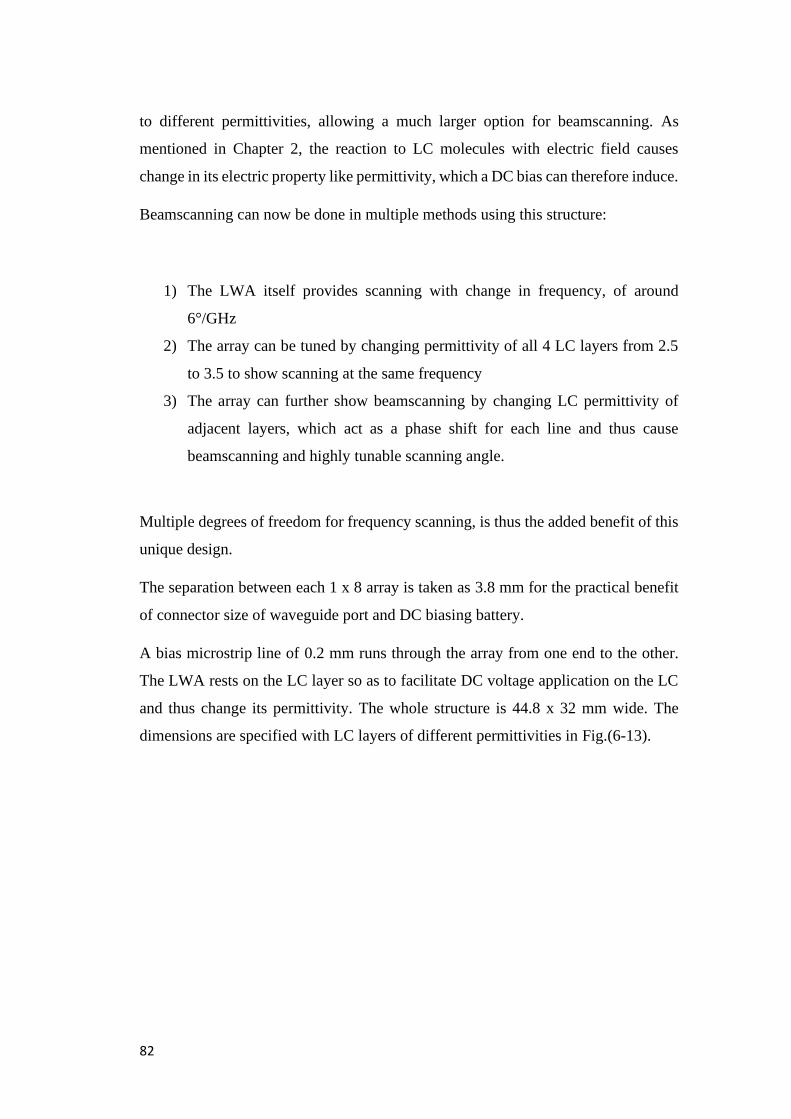
82
to different permittivities, allowing a much larger option for beamscanning. As
mentioned in Chapter 2, the reaction to LC molecules with electric field causes
change in its electric property like permittivity, which a DC bias can therefore induce.
Beamscanning can now be done in multiple methods using this structure:
1) The LWA itself provides scanning with change in frequency, of around
6°/GHz
2) The array can be tuned by changing permittivity of all 4 LC layers from 2.5
to 3.5 to show scanning at the same frequency
3) The array can further show beamscanning by changing LC permittivity of
adjacent layers, which act as a phase shift for each line and thus cause
beamscanning and highly tunable scanning angle.
Multiple degrees of freedom for frequency scanning, is thus the added benefit of this
unique design.
The separation between each 1 x 8 array is taken as 3.8 mm for the practical benefit
of connector size of waveguide port and DC biasing battery.
A bias microstrip line of 0.2 mm runs through the array from one end to the other.
The LWA rests on the LC layer so as to facilitate DC voltage application on the LC
and thus change its permittivity. The whole structure is 44.8 x 32 mm wide. The
dimensions are specified with LC layers of different permittivities in Fig.(6-13).
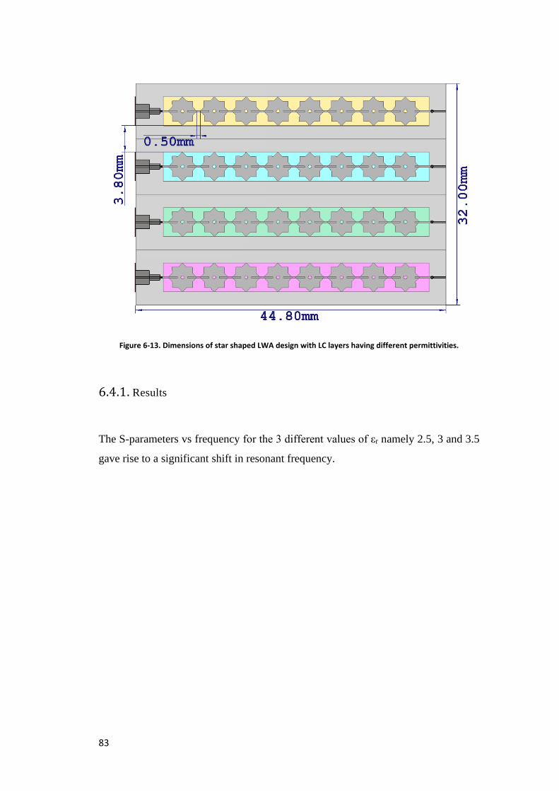
83
Figure 6-13. Dimensions of star shaped LWA design with LC layers having different permittivities.
6.4.1. Results
The S-parameters vs frequency for the 3 different values of εr namely 2.5, 3 and 3.5
gave rise to a significant shift in resonant frequency.
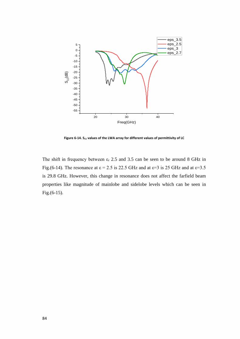
84
Figure 6-14. S11 values of the LWA array for different values of permittivity of LC
The shift in frequency between εr 2.5 and 3.5 can be seen to be around 8 GHz in
Fig.(6-14). The resonance at ε = 2.5 is 22.5 GHz and at ε=3 is 25 GHz and at ε=3.5
is 29.8 GHz. However, this change in resonance does not affect the farfield beam
properties like magnitude of mainlobe and sidelobe levels which can be seen in
Fig.(6-15).
20 30 40
-55
-50
-45
-40
-35
-30
-25
-20
-15
-10
-5
0
5
S1
1(d
B)
Freq(GHz)
eps_3.5
eps_2.5
eps_3
eps_2.7
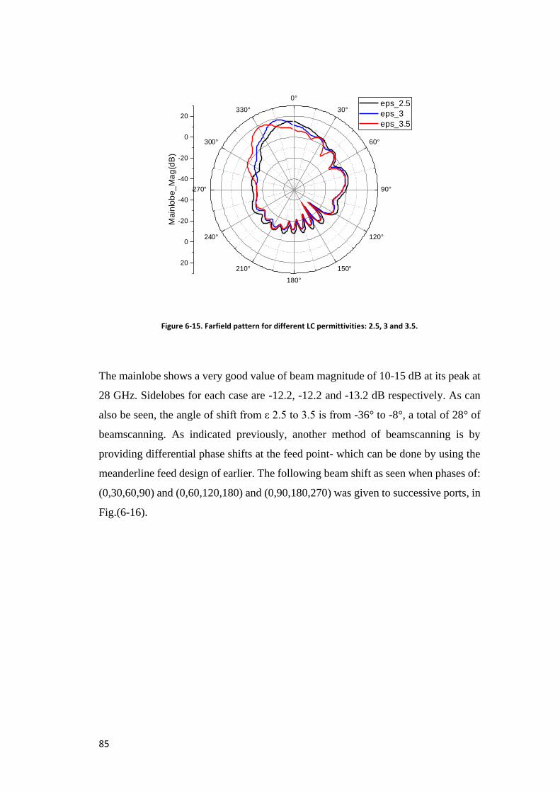
85
Figure 6-15. Farfield pattern for different LC permittivities: 2.5, 3 and 3.5.
The mainlobe shows a very good value of beam magnitude of 10-15 dB at its peak at
28 GHz. Sidelobes for each case are -12.2, -12.2 and -13.2 dB respectively. As can
also be seen, the angle of shift from ε 2.5 to 3.5 is from -36° to -8°, a total of 28° of
beamscanning. As indicated previously, another method of beamscanning is by
providing differential phase shifts at the feed point- which can be done by using the
meanderline feed design of earlier. The following beam shift as seen when phases of:
(0,30,60,90) and (0,60,120,180) and (0,90,180,270) was given to successive ports, in
Fig.(6-16).
0°
30°
60°
90°
120°
150°
180°
210°
240°
270°
300°
330°
-40
-20
0
20
-40
-20
0
20
Main
lob
e_
Ma
g(d
B)
eps_2.5
eps_3
eps_3.5
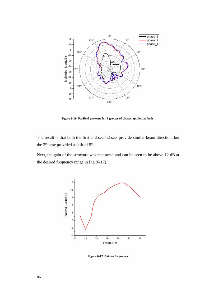
86
Figure 6-16. Farfield patterns for 3 groups of phases applied at feeds.
The result is that both the first and second sets provide similar beam direction, but
the 3rd case provided a shift of 5°.
Next, the gain of the structure was measured and can be seen to be above 12 dB at
the desired frequency range in Fig.(6-17).
Figure 6-17. Gain vs frequency
0°
30°
60°
90°
120°
150°
180°
210°
240°
270°
300°
330°
-30
-20
-10
0
10
20
-30
-20
-10
0
10
20
Main
lob
e_
Ma
g(d
B)
phase_3
phase_2
phase_1
20 22 24 26 28 30 32
-2
0
2
4
6
8
10
12
Rea
lize
d_G
ain
(dB
i)
Freq(GHz)
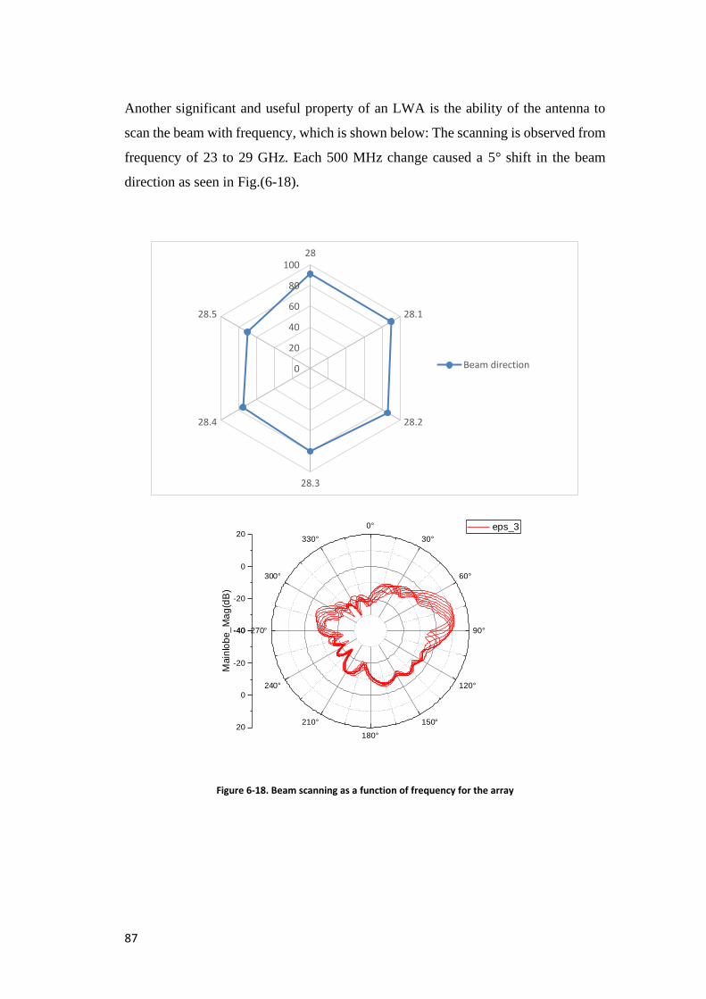
87
Another significant and useful property of an LWA is the ability of the antenna to
scan the beam with frequency, which is shown below: The scanning is observed from
frequency of 23 to 29 GHz. Each 500 MHz change caused a 5° shift in the beam
direction as seen in Fig.(6-18).
Figure 6-18. Beam scanning as a function of frequency for the array
0
20
40
60
80
10028
28.1
28.2
28.3
28.4
28.5
Beam direction
0°
30°
60°
90°
120°
150°
180°
210°
240°
270°
300°
330°
-40
-20
0
20
-40
-20
0
20
Main
lob
e_
Ma
g(d
B)
eps_3
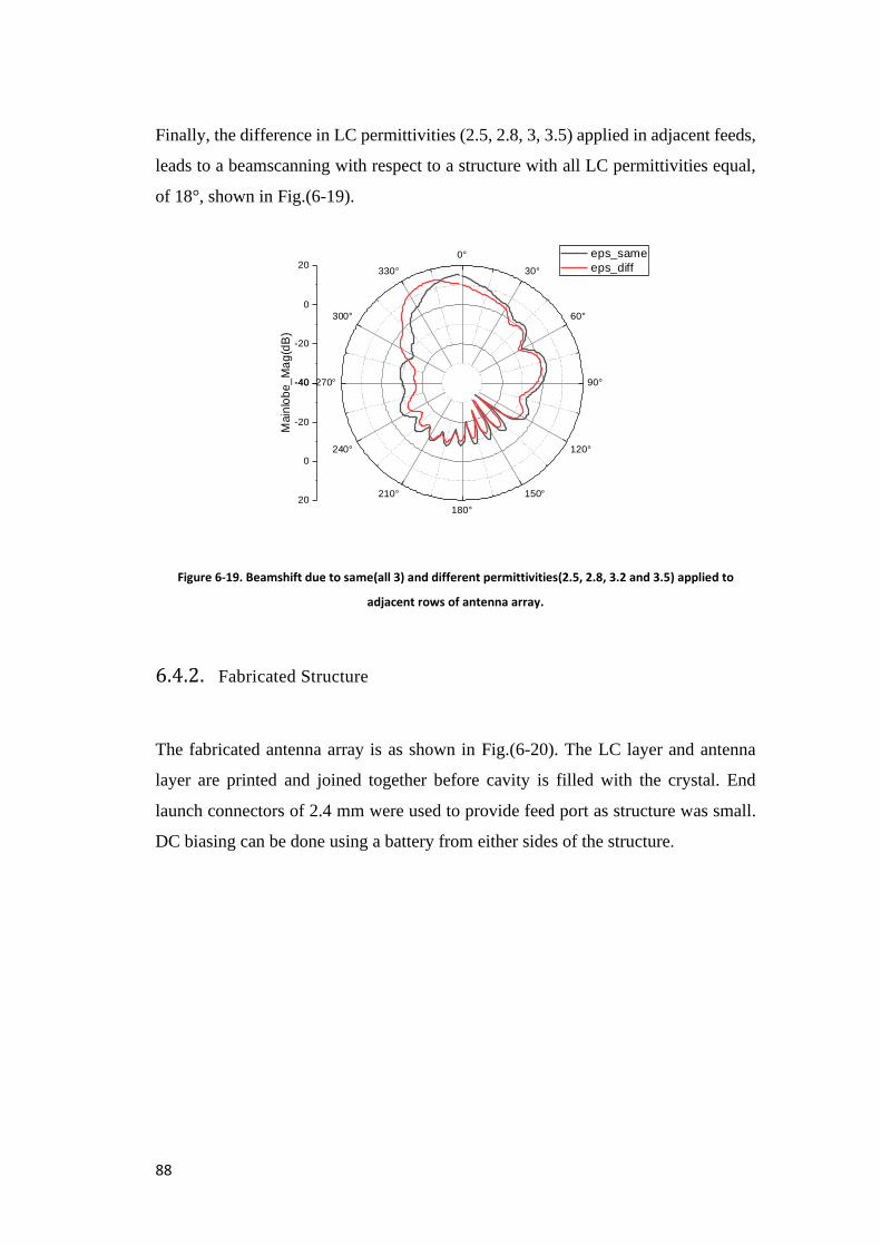
88
Finally, the difference in LC permittivities (2.5, 2.8, 3, 3.5) applied in adjacent feeds,
leads to a beamscanning with respect to a structure with all LC permittivities equal,
of 18°, shown in Fig.(6-19).
Figure 6-19. Beamshift due to same(all 3) and different permittivities(2.5, 2.8, 3.2 and 3.5) applied to
adjacent rows of antenna array.
6.4.2. Fabricated Structure
The fabricated antenna array is as shown in Fig.(6-20). The LC layer and antenna
layer are printed and joined together before cavity is filled with the crystal. End
launch connectors of 2.4 mm were used to provide feed port as structure was small.
DC biasing can be done using a battery from either sides of the structure.
0°
30°
60°
90°
120°
150°
180°
210°
240°
270°
300°
330°
-40
-20
0
20
-40
-20
0
20
Main
lob
e_
Ma
g(d
B)
eps_same
eps_diff
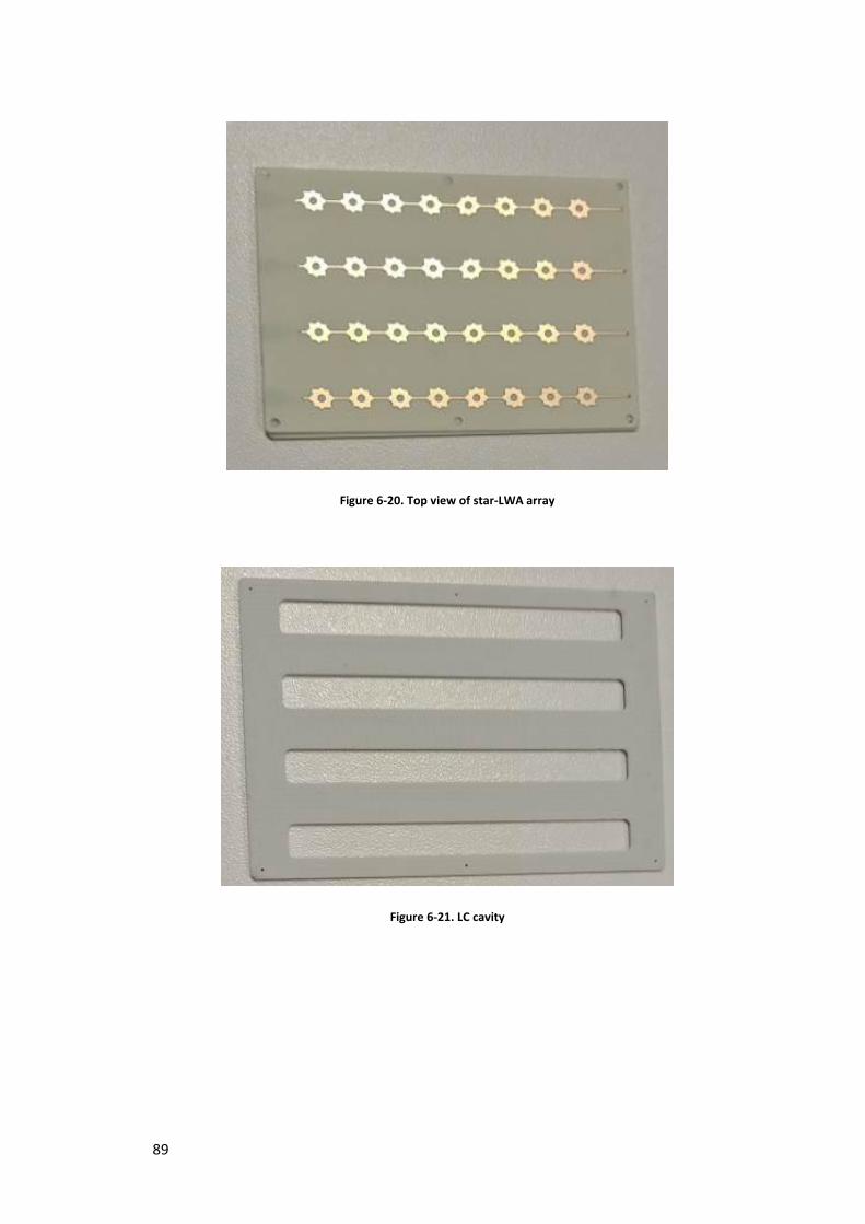
89
Figure 6-20. Top view of star-LWA array
Figure 6-21. LC cavity
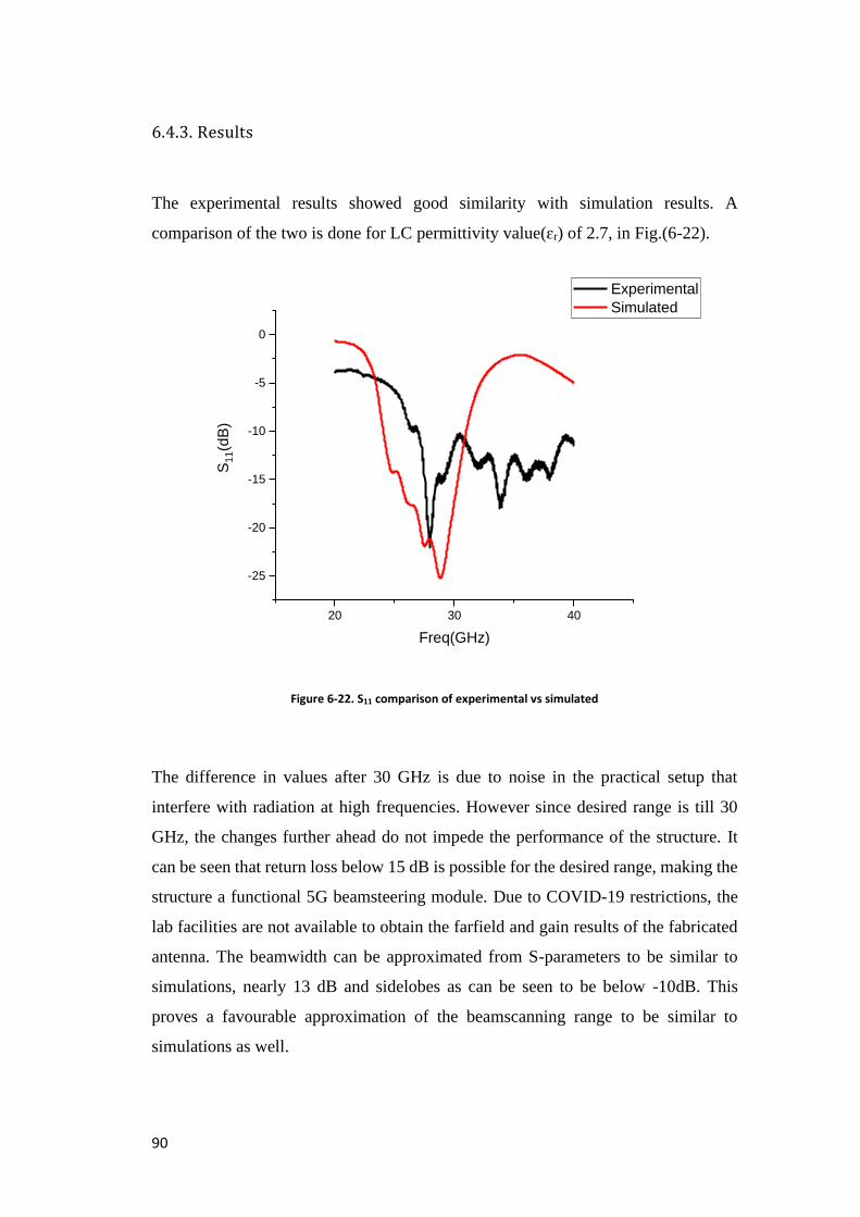
90
6.4.3. Results
The experimental results showed good similarity with simulation results. A
comparison of the two is done for LC permittivity value(ɛr) of 2.7, in Fig.(6-22).
Figure 6-22. S11 comparison of experimental vs simulated
The difference in values after 30 GHz is due to noise in the practical setup that
interfere with radiation at high frequencies. However since desired range is till 30
GHz, the changes further ahead do not impede the performance of the structure. It
can be seen that return loss below 15 dB is possible for the desired range, making the
structure a functional 5G beamsteering module. Due to COVID-19 restrictions, the
lab facilities are not available to obtain the farfield and gain results of the fabricated
antenna. The beamwidth can be approximated from S-parameters to be similar to
simulations, nearly 13 dB and sidelobes as can be seen to be below -10dB. This
proves a favourable approximation of the beamscanning range to be similar to
simulations as well.
20 30 40
-25
-20
-15
-10
-5
0
S1
1(d
B)
Freq(GHz)
Experimental
Simulated
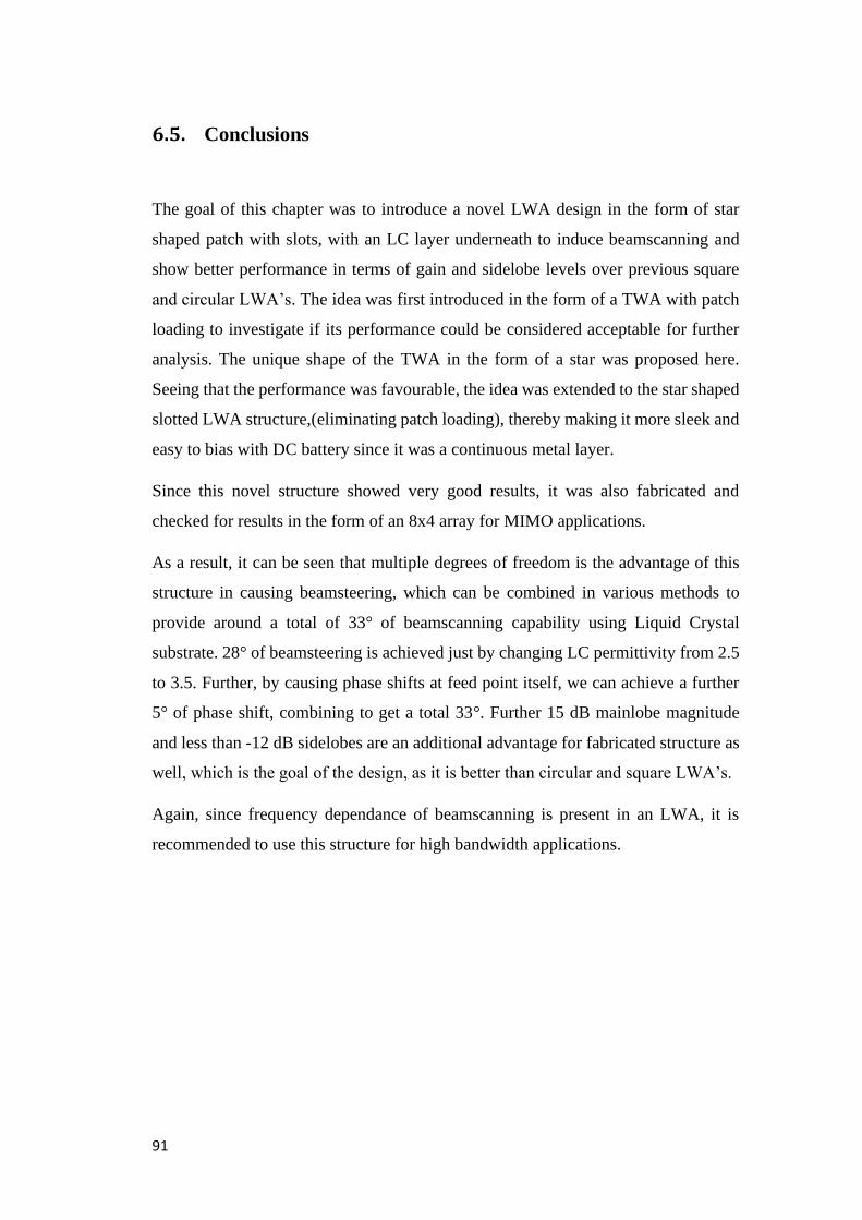
91
6.5. Conclusions
The goal of this chapter was to introduce a novel LWA design in the form of star
shaped patch with slots, with an LC layer underneath to induce beamscanning and
show better performance in terms of gain and sidelobe levels over previous square
and circular LWA’s. The idea was first introduced in the form of a TWA with patch
loading to investigate if its performance could be considered acceptable for further
analysis. The unique shape of the TWA in the form of a star was proposed here.
Seeing that the performance was favourable, the idea was extended to the star shaped
slotted LWA structure,(eliminating patch loading), thereby making it more sleek and
easy to bias with DC battery since it was a continuous metal layer.
Since this novel structure showed very good results, it was also fabricated and
checked for results in the form of an 8x4 array for MIMO applications.
As a result, it can be seen that multiple degrees of freedom is the advantage of this
structure in causing beamsteering, which can be combined in various methods to
provide around a total of 33° of beamscanning capability using Liquid Crystal
substrate. 28° of beamsteering is achieved just by changing LC permittivity from 2.5
to 3.5. Further, by causing phase shifts at feed point itself, we can achieve a further
5° of phase shift, combining to get a total 33°. Further 15 dB mainlobe magnitude
and less than -12 dB sidelobes are an additional advantage for fabricated structure as
well, which is the goal of the design, as it is better than circular and square LWA’s.
Again, since frequency dependance of beamscanning is present in an LWA, it is
recommended to use this structure for high bandwidth applications.
92
CHAPTER 7
CONCLUSIONS AND FUTURE WORK
5G defined various new techniques to achieve the high data rates, speed and low
latency solutions for products including massive MIMO beamscanning. In this work,
different types of antennas and their working with liquid crystals to enable
beamsteering is studied.
Commercially available Liquid Crystal compounds are compared and their chemical
properties are used to create the material for simulation tests. The commonly seen
range of permittivity of LC (e.g.: 5CB, Merck KGaA) between 2.5 and 3.5 is used in
the comparison of beamsteering of all antenna types.
Beginning with a meanderline based design for comparison of phase difference
obtainable for the defined range, we were able to observe a Figure of Merit of 61°/dB
for the meanderline design with embedded LC layer, ie, a phase shift of 85° for
permittivity change from 2.5 to 3.5. This was compared with another common phase
shift method of an interdigitated capacitor which are commonly seen in Leaky Wave
designs, combined with LC layer. The defined phase shifter could be used on a variety
of antenna structures since it was designed for the feed area and can be easily
integrated to an existing structure without adding complexity.
The patch antenna was considered to see the possible beamscanning since it was the
most commonly used structure for MIMO applications due to their form factor and
low cost of fabrication. When applied to a patch antenna array, the meanderline feed
design showed a phase shift of 9° for a 1 x 4 patch array. Sidelobes below 12 dB was
also achieved in all cases of permittivity. For a 4 x 4 array, the shift was increased to
17° for the same configuration and change of permittivity. This proved a useful
design for application since the LC layer was embedded in a substrate and hence
biasing could be achieved. It also avails flexibility in design of shape and size of patch
since LC layer is only at the meanderline feed region.
A study on the shapes of LC cavities below a patch antenna that can give maximum
frequency tuning range showed a dumbelle/ I shaped cavity to show 400 MHz more
93
tuning range than a normal rectangular cavity, due to inclusion of fringing fields of a
patch antenna. This can be used in applications that require higher tuning range for
the same range of permittivity.
An improvement on the 4 x 4 array structure was done to remove backlobe and field
interference due to meanderline feed in the form of a flipped array that consisted of
adding the meanderline feed on a 3rd layer below the patch antenna, interconnected
by vias, and ground layer between them. This array showed 20° beam shift with lower
backlobe and highly directive beam.
The main issue of a patch antenna design is the narrowband characteristic of such
antennas that cause issues due to frequency shift. Thus, application of LC layer has
to be made at feed instead of below the radiating structure. This again opens up many
methods of creating innovating designs using the Liquid Crystal.
The next study was on leaky wave antennas which are very commonly used in
frequency scanning applications and in this study showed the superior advantage of
being able to provide a method of DC voltage application to LC layer due to their
continuous structure.
The 3 types of LWA shapes considered were: circular, square and star- shaped. Each
structure has different properties that make it favourable. The circular structure shows
10° of beamscanning and square shows 15° beamscanning range with embedded LC
layer. The star shaped LWA structure shows 21° shift. Due to higher shift, this
structure was extended to the form of an array of 4 x 8 elements. The resulting
structure could be made to achieve a total of 35° of beamscanning by providing phase
shifts at the feed line. This is a significant amount of beamscanning that can be
applied in MIMO technology.
The resonance shift of an LWA is also an issue that can cause problems in antenna
gain at various permittivities. More wideband designs can solve this issue although
current design is able to achieve 12 dBi gain.
Leaky wave designs are more difficult to fabricate than normal rectangular patch
antennas but are more compact and thus LWA based LC designs can also be
94
considered especially in mobile and IoT applications since they require compact and
planar designs.
The future of this work aims to eliminate the sidelobes and improve gain of the
antenna. The beam shift can also be investigated to be larger by changing shape or
parameters of the antenna array. LWA’s offer a field that enables a wide amount of
tenability in terms of shape of design. Thus, more innovative shapes of the patch can
be investigated.
One such consideration is a Grid Array Antenna (GAA) capable of working in
wideband mode. A grid array antenna (GAA) is a kind of planar array antenna made
up of multiple rectangular loops.
Grid antennas are non-resonant antennas with a single fire beam. It is made up of
many rectangular elements called grids with sides of 1 wavelength by 0.5 wavelength.
The shorter sides are considered radiating and longer sides act as transmission lines.
[53]
Grid antennas are wide-beam antennas used in broad frequency applications due to
their multiple resonance points within their frequency band.
The array consists of 16 radiating elements with 0.75λ spacing between the patches in
the same row. The configuration is shown in Fig.(7-1).
The Grid Antenna Array as shown in the figure below contains 16 square elements,
consisting of an LC layer of 0.25mm embedded in a thick ground plane of 1.50 mm
thickness and Rogers substrate of 0.25 mm on top. It was fed by through-hole feeding
technique using a coaxial cable, shown in Fig.(7-2).
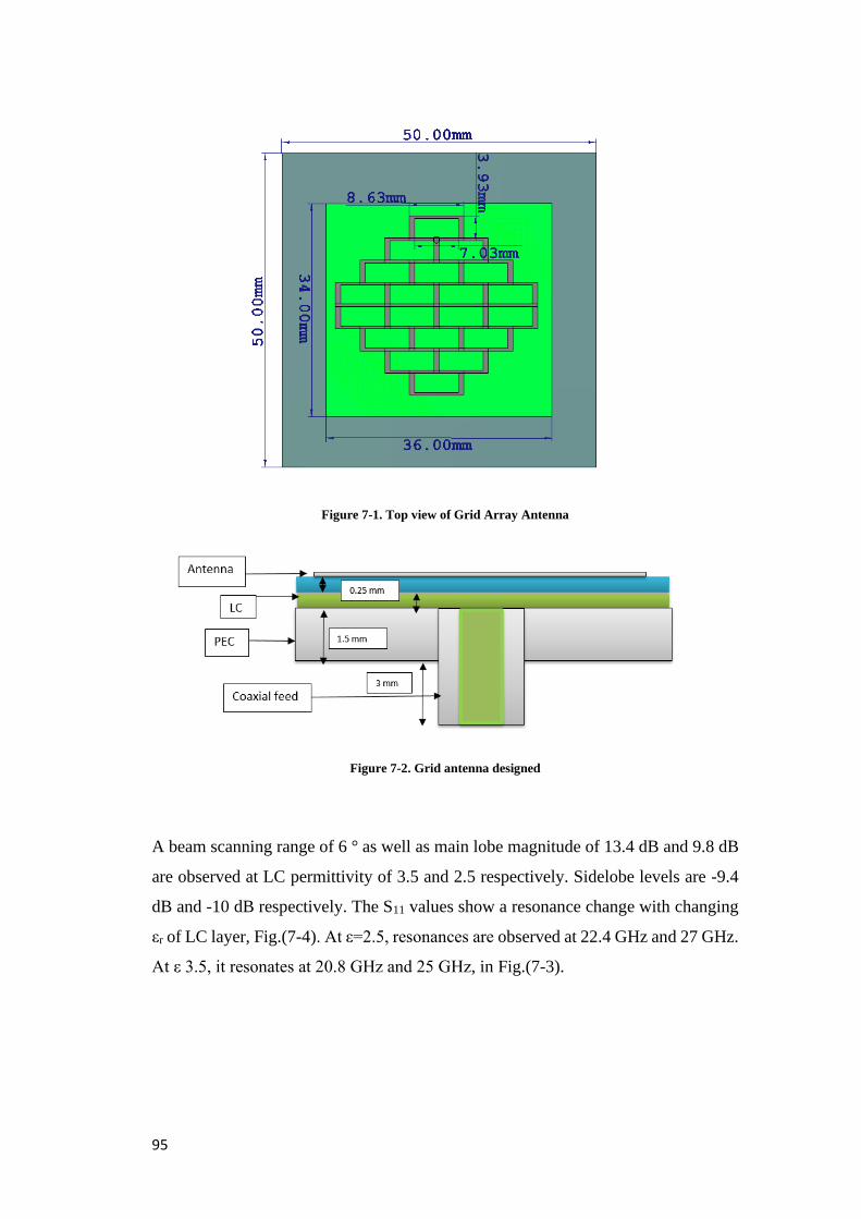
95
Figure 7-1. Top view of Grid Array Antenna
Figure 7-2. Grid antenna designed
A beam scanning range of 6 ° as well as main lobe magnitude of 13.4 dB and 9.8 dB
are observed at LC permittivity of 3.5 and 2.5 respectively. Sidelobe levels are -9.4
dB and -10 dB respectively. The S11 values show a resonance change with changing
εr of LC layer, Fig.(7-4). At ε=2.5, resonances are observed at 22.4 GHz and 27 GHz.
At ε 3.5, it resonates at 20.8 GHz and 25 GHz, in Fig.(7-3).
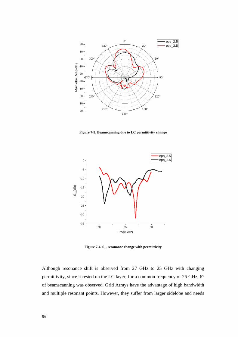
96
Figure 7-3. Beamscanning due to LC permittivity change
Figure 7-4. S11 resonance change with permittivity
Although resonance shift is observed from 27 GHz to 25 GHz with changing
permittivity, since it rested on the LC layer, for a common frequency of 26 GHz, 6°
of beamscanning was observed. Grid Arrays have the advantage of high bandwidth
and multiple resonant points. However, they suffer from larger sidelobe and needs
0°
30°
60°
90°
120°
150°
180°
210°
240°
270°
300°
330°
-20
-10
0
10
20
-20
-10
0
10
20
Main
lob
e_
Ma
g(d
B)
eps_2.5
eps_3.5
20 25 30
-35
-30
-25
-20
-15
-10
-5
0
S11(d
B)
Freq(GHz)
eps_3.5
eps_2.5
97
proper matching to be practically used. To conclude, GAA’s are an interesting series
of antennas that can be used in broadband applications but show limited
beamscanning range.
Metamaterial based LC designs are another popular trend in 5G design. This can be
extended to all the types of antennas discussed before.
A compromise between ease of fabrication, cost and beamsteering angle is to be
reached in practical design and more ideas are thus limited by these constraints.
However, LCs offer an easy and planar, integrable alternative to existing
beamscanning methods. Thus, it will be a source of more research and innovative
design for the future, of which this work will hope to be a good summary of the way
different types of antenna array configurations can be combined with LC layers.
98
AUTHOR’S PUBLICATIONS
[1] Kirshnan, Divya, A. Alphones, and Mei Sun. "Enhanced Frequency Tuning
based on Optimized Liquid Crystal Cavity based Patch Antenna." 2019 IEEE
Asia-Pacific Microwave Conference (APMC). IEEE, 2019.
[2] Krishnan, D., Alphones, A. ‘Liquid Crystal Material based Electronically
Beam Steering Antenna at Ka-band for 5G Applications’. 2020 Antenna and
Propagation Society Conference(AP-S), IEEE. (2020)
99
BIBLIOGRAPHY
[1] Wirth, Thomas, et al. "An advanced hardware platform to verify 5G wireless
communication concepts." 2015 IEEE 81st Vehicular Technology Conference
(VTC Spring). IEEE, 2015.
[2] Rodriguez, Jonathan. Fundamentals of 5G mobile networks. John Wiley & Sons,
2015.
[3] Penttinen, Jyrki. 5G Explained. Wiley, 2019.
[4] Xiang, Wei, Kan Zheng, and Xuemin Sherman Shen, eds. 5G mobile
communications. Springer, 2016.
[5] Nguyen, T. "Small Cell Networks and the Evolution of 5G." (2017).
[6] Nordrum, Amy, and Kristen Clark. "Everything you need to know about
5G." IEEE Spectrum 27 (2017).
[7] Pearson, Chris. " 5G Radios are Packed with Advanced Antenna
Technology." www.linkedin.com (2014).
[8] Bogale, T. E., X. Wang, and L. B. Le. "mmWave communication enabling
techniques for 5G wireless systems: A link level perspective." MmWave Massive
MIMO. Academic Press, 2017. 195-225.
[9] Fulton III, Scott. "What is 5G? The business guide to next-generation wireless
technology." ZD Net 19.09 (2019).
[10] Vahid, Seiamak, Rahim Tafazolli, and Marcin Filo. "Small cells for 5G mobile
networks." Fundamentals of 5G Mobile Networks (2015): 63-104.
[11] Leigh, Hartman. " Why is America Concerned About 5G?." share.america.gov
(2019).
[12] Wikipedia contributors. “5G”. www.wikipedia.com (2018).
[13] Flynn, Kevin. "Release 15." 3gpp. org (2019).
[14] AMTA, “5G Explained”. emfexplained.info (2019).
[15] Van Chien, Trinh, and Emil Björnson. "Massive MIMO communications." 5G
Mobile communications. Springer, cham, 2017. 77-116.
[16] Comba Telecom. “5G Massive MIMO Antenna & 3D Beamforming”.
www.comba-telecom.com(2018).
100
[17] Lu, Lu, et al. "An overview of massive MIMO: Benefits and challenges." IEEE
journal of selected topics in signal processing 8.5 (2014): 742-758.
[18] Aluko, Obadamilola. Frameworks to enhance performance in precoded multi-
user MIMO systems. Diss. Purdue University, 2010.
[19] Mundy, Jon, and Kevin Thomas. "What is massive MIMO
technology?." 5g.co.uk (2019): 1.
[20] EventHelix. “Massive MIMO”. www.medium.com (2017).
[21] Metaswitch “What is 5G beamforming, beam steering and beam switching with
massive MIMO”, www.metaswitch.com (2019).
[22] Bogale, T. E., X. Wang, and L. B. Le. "mmWave communication enabling
techniques for 5G wireless systems: A link level perspective." MmWave Massive
MIMO. Academic Press, 2017. 195-225.
[23] Cavazos, Jessy. “5G Testing: 3GPP Beam Management”, www.keysight.com
(2019).
[24] Uchendu, Iyemeh, and James R. Kelly. "Survey of beam steering techniques
available for millimeter wave applications." Progress In Electromagnetics
Research 68 (2016): 35-54.
[25] Sakakibara, Kunio, and Guy Kouemou. "High-Gain Millimeter-Wave Planar
Array Antennas with Traveling-Wave Excitation." Radar Technology (2009):
319-340.
[26] Güneş, Filiz, Aysu Belen, and Mehmet A. Belen. "Microstrip tapered traveling
wave antenna for wide range of beam scanning in X‐and Ku‐
bands." International Journal of RF and Microwave Computer‐Aided
Engineering 29.9 (2019): e21771.
[27] Karmokar, Debabrata K., et al. "Composite Right/Left-Handed Leaky-Wave
Antennas for Wide-Angle Beam Scanning With Flexibly Chosen Frequency
Range." IEEE Transactions on Antennas and Propagation 68.1 (2019): 100-110.
[28] Symeonidou, Athanasia, and Katherine Siakavara. "A novel microstrip antenna
array with metamaterial-based electronic beam steering at 2.4 GHz." Progress In
Electromagnetics Research 38 (2013): 27-42.
[29] Yang, Deng-Ke, and Shin-Tson Wu. Fundamentals of liquid crystal devices.
John Wiley & Sons, 2014.
101
[30] Borshch, Volodymyr, Sergij V. Shiyanovskii, and Oleg D. Lavrentovich.
"Nanosecond electro-optic switching of a liquid crystal." Physical review
letters 111.10 (2013): 107802.
[31] Borner, Ruth C., et al. "The synthesis of triphenylene‐based discotic mesogens
New and improved routes." Liquid Crystals 33.11-12 (2006): 1439-1448.
[32] Averill, B. A., and P. Eldredge. "Principles of General Chemistry, online."
(2012).
[33] Yang, Deng-Ke, and Shin-Tson Wu. Fundamentals of liquid crystal devices.
John Wiley & Sons, 2014.
[34] Wikipedia contributors. Liquid crystal. www.wikipedia.com (2014).
[35] Yaghmaee, Pouria, et al. "Electrically tuned microwave devices using liquid
crystal technology." International Journal of Antennas and Propagation 2013
(2013).
[36] Karabey, O. H., et al. "Liquid crystal based phased array antenna with improved
beam scanning capability." Electronics letters 50.6 (2014): 426-428.
[37] Marin, R., et al. "77 GHz reconfigurable reflectarray with nematic liquid
crystal." (2007): 9-9.
[38] Chieh, Jia-Chi Samuel. Development of Advanced Microwave/Millimeter-Wave
Multi-Antenna Systems on Liquid Crystal Polymer. University of California,
Davis, 2012.
[39] Deo, Prafulla, and Dariush Mirshekar-Syahkal. "60 GHz beam-steering slotted
patch antenna array using liquid crystal phase-shifters." Proceedings of the 2012
IEEE International Symposium on Antennas and Propagation. IEEE, 2012.
[40] Che, Bang-Jun, et al. "Electrically controllable composite right/left-handed
leaky-wave antenna using liquid crystals in PCB technology." IEEE
Transactions on Components, Packaging and Manufacturing Technology 7.8
(2017): 1331-1342.
[41] Yang, Shih-Ming, and Chih-Hsin Huang. "An Inductor Model for Analyzing the
Performance of Printed Meander Line Antennas in Smart Structures." Journal of
Electromagnetic Analysis and applications 6.09 (2014): 244.
102
[42] Maki, D. W., and Mario Siracusa. "Design of interdigitated capacitors and Their
application to gallium arsenide monolithic filters." IEEE Transactions on
Microwave Theory and Techniques 83.1 (1983): 57-64.
[43] Pandian, Manickam K., and Thangam Chinnadurai. "Design and Optimization of
Rectangular Patch Antenna Based on FR4, Teflon and Ceramic
Substrates." Recent Advances in Electrical & Electronic Engineering (Formerly
Recent Patents on Electrical & Electronic Engineering) 12.4 (2019): 368-373.
[44] Rahmatia, Suci, et al. "Designing dipole antenna for TV application and
rectangular microstrip antenna working at 3 GHz for radar application." 2017 5th
International Conference on Cyber and IT Service Management (CITSM). IEEE,
2017.
[45] Mehta, Anuj. "Microstrip antenna." International Journal of Scientific &
Technology Research 4.3 (2015): 54-57.
[46] Kirshnan, Divya, A. Alphones, and Mei Sun. "Enhanced Frequency Tuning
based on Optimized Liquid Crystal Cavity based Patch Antenna." 2019 IEEE
Asia-Pacific Microwave Conference (APMC). IEEE, 2019.
[47] Sangster, Alan J. Compact Slot Array Antennas for Wireless Communications.
Springer International Publishing, 2019.
[48] Maasch, Matthias. Tunable microwave metamaterial structures. Springer, 2016.
[49] Choi, Jun H., et al. "Beam-scanning leaky-wave antennas." Handbook of Antenna
Technologies (2016): 1-33.
[50] Habaebi, Mohamed Hadi, Mohanad Janat, and Md Rafiqul Islam. "Beam steering
antenna array for 5G telecommunication systems applications." Progress In
Electromagnetics Research 67 (2018): 197-207.
[51] Balanis, Constantine A. Antenna theory: analysis and design. John wiley & sons,
2016.
[52] Güneş, Filiz, Aysu Belen, and Mehmet A. Belen. "Microstrip tapered traveling
wave antenna for wide range of beam scanning in X‐and Ku‐
bands." International Journal of RF and Microwave Computer‐Aided
Engineering 29.9 (2019): e21771.
103
[53] Chen, Xing, Guosheng Wang, and Kama Huang. "A novel wideband and
compact microstrip grid array antenna." IEEE transactions on antennas and
propagation 58.2 (2010): 596-599.