Embed Size (px)
Citation preview
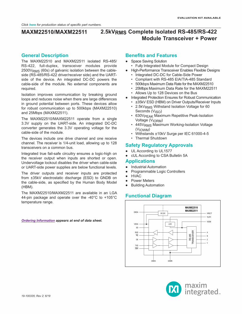
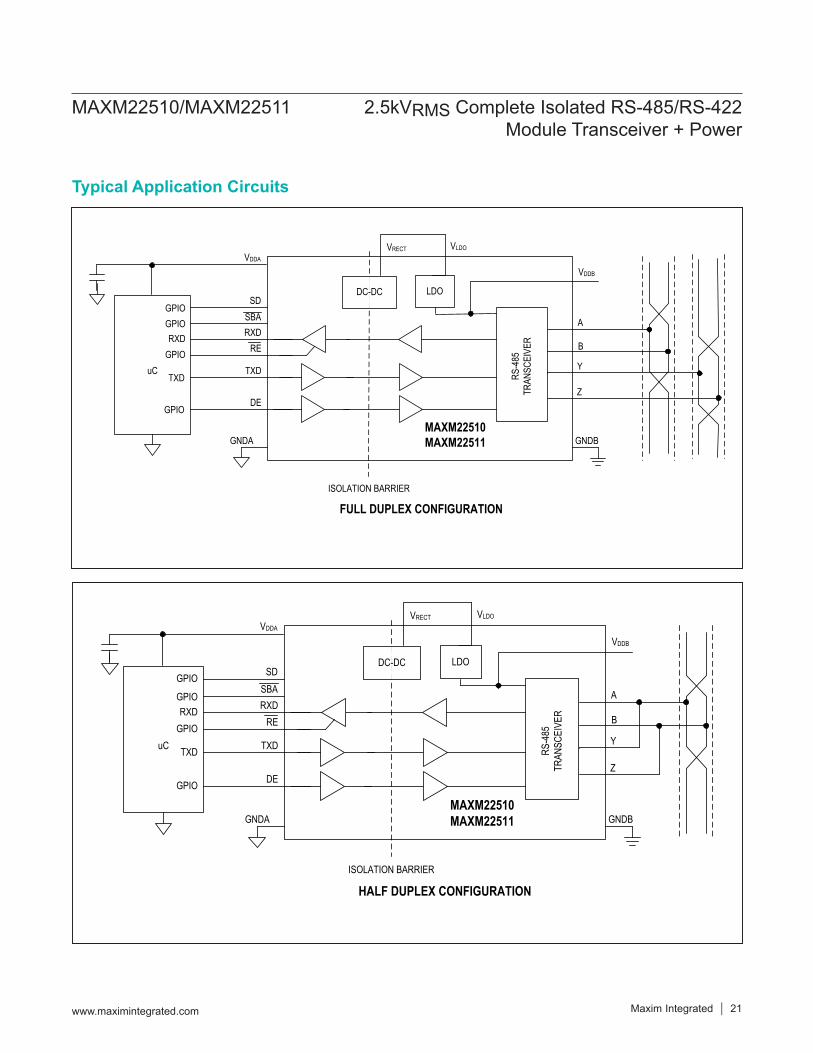
General DescriptionThe MAXM22510 and MAXM22511 isolated RS-485/RS-422, full-duplex, transceiver modules provide 2500VRMS (60s) of galvanic isolation between the cable-side (RS-485/RS-422 driver/receiver side) and the UART-side of the device. An integrated DC-DC powers the cable-side of the module. No external components are required. Isolation improves communication by breaking ground loops and reduces noise when there are large differences in ground potential between ports. These devices allow for robust communication up to 500kbps (MAXM22510) and 25Mbps (MAXM22511).The MAXM22510/MAXM22511 operate from a single 3.3V supply on the UART-side. An integrated DC-DC converter generates the 3.3V operating voltage for the cable-side of the module.The devices include one drive channel and one receive channel. The receiver is 1/4-unit load, allowing up to 128 transceivers on a common bus.Integrated true fail-safe circuitry ensures a logic-high on the receiver output when inputs are shorted or open. Undervoltage lockout disables the driver when cable-side or UART-side power supplies are below functional levels. The driver outputs and receiver inputs are protected from ±35kV electrostatic discharge (ESD) to GNDB on the cable-side, as specified by the Human Body Model (HBM).The MAXM22510/MAXM22511 are available in an LGA 44-pin package and operate over the -40°C to +105°C temperature range.
Benefits and Features Space Saving Solution
• Fully Integrated Module for Compact Design High-Performance Transceiver Enables Flexible Designs
• Integrated DC-DC for Cable-Side Power• Compliant with RS-485 EIA/TIA-485 Standard• 500kbps Maximum Data Rate for the MAXM22510• 25Mbps Maximum Data Rate for the MAXM22511 • Allows Up to 128 Devices on the Bus
Integrated Protection Ensures for Robust Communication• ±35kV ESD (HBM) on Driver Outputs/Receiver Inputs• 2.5kVRMS Withstand Isolation Voltage for 60
Seconds (VISO)• 630VPEAK Maximum Repetitive Peak-Isolation
Voltage (VIORM)• 445VRMS Maximum Working-Isolation Voltage
(VIOWM)• Withstands ±10kV Surge per IEC 61000-4-5• Thermal Shutdown
Safety Regulatory Approvals UL According to UL1577 cUL According to CSA Bulletin 5A
Applications Industrial Automation Programmable Logic Controllers HVAC Power Meters Building Automation
Ordering Information appears at end of data sheet.
19-100335; Rev 2; 6/19
Click here for production status of specific part numbers.
LDO
RS-
485
TRAN
SCEI
VER
VDDA
RXD
RE
TXD
DE
A
B
VDDB
VLDO
GNDA GNDB
MAXM22510MAXM22511
SD
Z
Y
DC-DC VRECTGNDA
SBA
MAXM22510/MAXM22511 2.5kVRMS Complete Isolated RS-485/RS-422 Module Transceiver + Power
Functional Diagram
EVALUATION KIT AVAILABLE
VDDA to GNDA .......................................................-0.3V to +4VVDDB to GNDB ........................................................-0.3V to +6VVRECT, VLDO to GNDB ...........................................-0.3V to +8VSD, TXD, DE, RE to GNDA ....................................-0.3V to +6VSBA, RXD to GNDA .............................. -0.3V to (VDDA + 0.3V)A, B, Y, Z to GNDB ...................................................-8V to +13VShort-Circuit Duration (RXD, SBA to GNDA, A, B, Y, Z ,VDDB to GNDB) ....................................Continuous
Continuous Power Dissipation (TA = +70°C) 44-pin LGA (derate 28.6mW/°C above +70°C) .........2286mW
Operating Temperature Range ......................... -40°C to +105°CJunction Temperature ......................................................+125°CStorage Temperature Range ............................ -65°C to +125°CSoldering Temperature (reflow) .......................................+245°C
DC Electrical Characteristics(VDDA – VGNDA = 3.0V to 3.6V, TA = TMIN to TMAX, unless otherwise noted. Typical values are at VDDA – VGNDA = 3.3V, VGNDA = VGNDB, and TA = +25°C.) (Notes 1, 2)
PACKAGE TYPE: 44 LGAPackage Code L44119M+1Outline Number 21-100226Land Pattern Number 90-100107THERMAL RESISTANCE, FOUR-LAYER BOARDJunction to Ambient (θJA) 48°C/WJunction to Case (θJC) (top) 39.2°C/W
PARAMETER SYMBOL CONDITIONS MIN TYP MAX UNITS
POWER
Supply Voltage VDDA 3.0 3.6 V
Supply Current IDDA
VDDA = 3.3V, DE = high, RE = TXD = low, SD = low, RXD unconnected, no load
25 44 mA
Shutdown Supply Current ISD VDDA = 3.3V, SD = high 0.01 10 μA
Undervoltage Lockout Threshold
VUVLOA VDDA rising 2.55 2.7 2.85V
VUVLOB VDDB rising 2.55 2.7 2.85
Undervoltage Lockout Threshold Hysteresis
VUVHYSTA 200mV
VUVHYSTB 200Unregulated DC-DC Output Voltage VRECT
VDDA = 3.3V, DE = high, RE = TXD = low, SD = low, no load 6 V
www.maximintegrated.com Maxim Integrated 2
MAXM22510/MAXM22511 2.5kVRMS Complete Isolated RS-485/RS-422 Module Transceiver + Power
Package thermal resistances were obtained using the method described in JEDEC specification JESD51-7, using a four-layer board. For detailed information on package thermal considerations, refer to www.maximintegrated.com/thermal-tutorial.
For the latest package outline information and land patterns (footprints), go to www.maximintegrated.com/packages. Note that a “+”, “#”, or “-” in the package code indicates RoHS status only. Package drawings may show a different suffix character, but the drawing pertains to the package regardless of RoHS status.
Absolute Maximum Ratings
Package Information
Stresses beyond those listed under “Absolute Maximum Ratings” may cause permanent damage to the device. These are stress ratings only, and functional operation of the device at these or any other conditions beyond those indicated in the operational sections of the specifications is not implied. Exposure to absolute maximum rating conditions for extended periods may affect device reliability.
DC Electrical Characteristics (continued)(VDDA – VGNDA = 3.0V to 3.6V, TA = TMIN to TMAX, unless otherwise noted. Typical values are at VDDA – VGNDA = 3.3V, VGNDA = VGNDB, and TA = +25°C.) (Notes 1, 2)
PARAMETER SYMBOL CONDITIONS MIN TYP MAX UNITS
LDO
LDO Output Voltage VDDB 3.0 3.3 3.6 V
LDO Current Limit 300 mA
Load Regulation VLDO = 3.3V, ILOAD = -20mA to -40mA 0.19 1.7 mV/mA
Line Regulation VLDO = 3.3V to 7.5V, ILOAD = -20mA 0.12 mV/VDropout Voltage VLDO = 3.18V, IDDB = -120mA 100 180 mV
Load Capacitance Nominal value (Note 3) 1 10 µF
LOGIC INTERFACE (TXD, RXD, DE, RE, SD, SBA)
Input High Voltage VIH RE, TXD, DE, SD to GNDA 0.7 x VDDA
V
Input Low Voltage VIL RE, TXD, DE, SD to GNDA 0.8 V
Input Hysteresis VHYS RE, TXD, DE, SD to GNDA 220 mV
Input Capacitance CIN RE, TXD, DE, SD, f = 1MHz 2 pF
Input Pullup Current IPU TXD, SD -10 -4.5 -1.5 µA
Input Pulldown Current IPD DE, RE 1.5 4.5 10 µA
SBA Pullup Resistance RSBA 3 5 8 kΩ
Output Voltage High VOH RXD to GNDA, IOUT = -4mA VDDA -0.4 V
Output Voltage Low VOLRXD to GNDA, IOUT = 4mA 0.40
VSBA to GNDA, IOUT = 4mA 0.45
Short-Circuit Output Pullup Current ISH_PU
0V ≤ VRXD ≤ VDDA, (VA - VB) > -10mV, RE = low -42 mA
Short-Circuit Output Pulldown Current ISH_PD
0V ≤ VRXD ≤ VDDA, (VA - VB) < -200mV, RE = low 42
mA0V ≤ VSBA ≤ VDDA, SBA is asserted 60
Three-State Output Current IOZ 0V ≤ VRXD ≤ VDDA, RE = high -1 +1 µA
DRIVER
Differential Driver Output |VOD|
RL = 54Ω, TXD = high or low, Figure 1a 1.5
VRL = 100Ω, TXD = high or low, Figure 1a 2.0
-7V ≤ VCM ≤ +12V, Figure 1b 1.5 5
Change in Magnitude of Differ-ential Driver Output Voltage ΔVOD RL = 100Ω or 54Ω, Figure 1a (Note 4) 0.2 V
www.maximintegrated.com Maxim Integrated 3
MAXM22510/MAXM22511 2.5kVRMS Complete Isolated RS-485/RS-422 Module Transceiver + Power
DC Electrical Characteristics (continued)(VDDA – VGNDA = 3.0V to 3.6V, TA = TMIN to TMAX, unless otherwise noted. Typical values are at VDDA – VGNDA = 3.3V, VGNDA = VGNDB, and TA = +25°C.) (Notes 1, 2)
PARAMETER SYMBOL CONDITIONS MIN TYP MAX UNITSDriver Common-Mode Output Voltage VOC RL = 100Ω or 54Ω, Figure 1a VDDB/ 2 3 V
Change in Magnitude of Common-Mode Voltage ΔVOC RL = 100Ω or 54Ω, Figure 1a (Note 4) 0.2 V
Driver Short-Circuit Output Current IOSD
GNDB ≤ VOUT ≤ +12V, output low (Note 5) +30 +250
mA-7V ≤ VOUT ≤ VDDB, output high (Note 5) -250 -30
Single-Ended Driver Output Voltage High VOH Y and Z outputs, IY,Z = -20mA 2.2 V
Single-Ended Driver Output Voltage Low VOL Y and Z outputs, IY,Z = +20mA 0.8 V
Differential Driver Output Capacitance COD DE = RE = high, f = 4MHz 12 pF
RECEIVER
Input Current (A and B) IA, IBDE = low, VDDB = GNDB or 3.6V
VIN = +12V +250µA
VIN = -7V -200Receiver Differential Threshold Voltage VTH -7V ≤ VCM ≤ +12V -200 -120 -10 mV
Receiver Input Hysteresis ΔVTH VCM = 0V 20 mV
Receiver Input Resistance RIN -7V ≤ VCM ≤ +12V, DE = low 48 kΩ
Differential Input Capacitance CA,BMeasured between A and B, DE = RE = low, f = 6MHz 12 pF
PROTECTIONThermal Shutdown Threshold TSHDN Temperature Rising +160 °C
Thermal Shutdown Hysteresis THYST 15 °C
ESD Protection (A, B, Y, Z Pins to GNDB)
Human Body Model ±35
kVIEC 61000-4-2 Air Gap Discharge ±18
IEC 61000-4-2 Contact Discharge ±8
ESD Protection (A, B, Y, Z Pins to GNDA)
Human Body Model ±6kV
330pF capacitor from GNDB to GNDA ±20
ESD Protection (All Other Pins) Human Body Model ±4 kV
www.maximintegrated.com Maxim Integrated 4
MAXM22510/MAXM22511 2.5kVRMS Complete Isolated RS-485/RS-422 Module Transceiver + Power
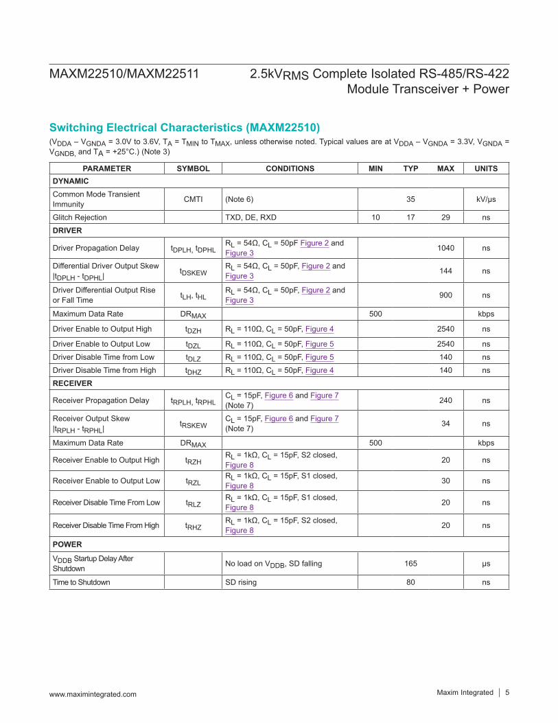
Switching Electrical Characteristics (MAXM22510)(VDDA – VGNDA = 3.0V to 3.6V, TA = TMIN to TMAX, unless otherwise noted. Typical values are at VDDA – VGNDA = 3.3V, VGNDA = VGNDB, and TA = +25°C.) (Note 3)
PARAMETER SYMBOL CONDITIONS MIN TYP MAX UNITSDYNAMICCommon Mode Transient Immunity CMTI (Note 6) 35 kV/μs
Glitch Rejection TXD, DE, RXD 10 17 29 nsDRIVER
Driver Propagation Delay tDPLH, tDPHLRL = 54Ω, CL = 50pF Figure 2 and Figure 3 1040 ns
Differential Driver Output Skew |tDPLH - tDPHL| tDSKEW
RL = 54Ω, CL = 50pF, Figure 2 and Figure 3 144 ns
Driver Differential Output Rise or Fall Time tLH, tHL
RL = 54Ω, CL = 50pF, Figure 2 and Figure 3 900 ns
Maximum Data Rate DRMAX 500 kbps
Driver Enable to Output High tDZH RL = 110Ω, CL = 50pF, Figure 4 2540 ns
Driver Enable to Output Low tDZL RL = 110Ω, CL = 50pF, Figure 5 2540 nsDriver Disable Time from Low tDLZ RL = 110Ω, CL = 50pF, Figure 5 140 nsDriver Disable Time from High tDHZ RL = 110Ω, CL = 50pF, Figure 4 140 nsRECEIVER
Receiver Propagation Delay tRPLH, tRPHLCL = 15pF, Figure 6 and Figure 7 (Note 7) 240 ns
Receiver Output Skew|tRPLH - tRPHL| tRSKEW
CL = 15pF, Figure 6 and Figure 7 (Note 7) 34 ns
Maximum Data Rate DRMAX 500 kbps
Receiver Enable to Output High tRZHRL = 1kΩ, CL = 15pF, S2 closed, Figure 8 20 ns
Receiver Enable to Output Low tRZLRL = 1kΩ, CL = 15pF, S1 closed, Figure 8 30 ns
Receiver Disable Time From Low tRLZRL = 1kΩ, CL = 15pF, S1 closed, Figure 8 20 ns
Receiver Disable Time From High tRHZRL = 1kΩ, CL = 15pF, S2 closed, Figure 8 20 ns
POWER
VDDB Startup Delay After Shutdown No load on VDDB, SD falling 165 µs
Time to Shutdown SD rising 80 ns
www.maximintegrated.com Maxim Integrated 5
MAXM22510/MAXM22511 2.5kVRMS Complete Isolated RS-485/RS-422 Module Transceiver + Power
Note 1: All devices are 100% production tested at TA = +25°C. Specifications over temperature are guaranteed by design and char-acterization.
Note 2: All currents into the device are positive. All currents out of the device are negative. All voltages are referenced to their respective ground (GNDA or GNDB), unless otherwise noted.
Note 3: Not production tested. Guaranteed by design and characterization.Note 4: ΔVOD and ΔVOC are the changes in |VOD| and VOC, respectively, when the TXD input changes state. Note 5: The short circuit output current applies to the peak current just prior to current limiting.
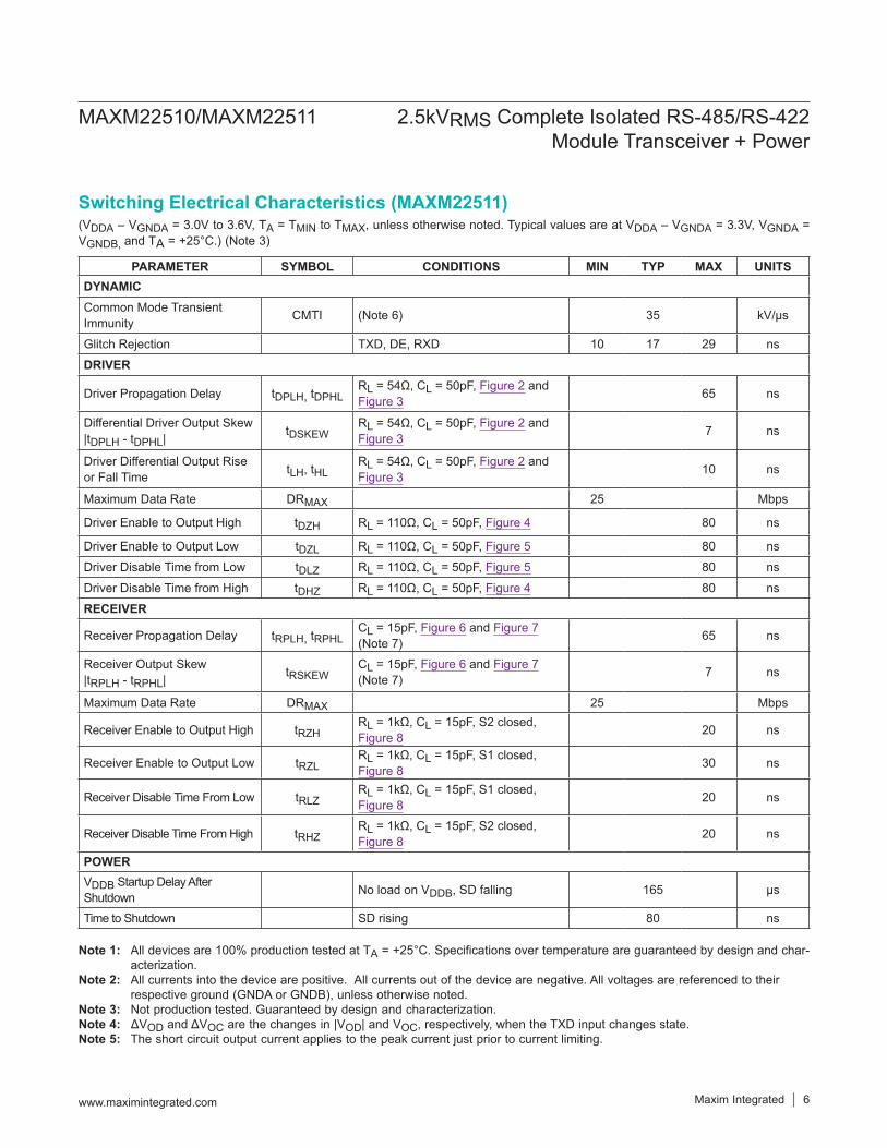
Switching Electrical Characteristics (MAXM22511)(VDDA – VGNDA = 3.0V to 3.6V, TA = TMIN to TMAX, unless otherwise noted. Typical values are at VDDA – VGNDA = 3.3V, VGNDA = VGNDB, and TA = +25°C.) (Note 3)
PARAMETER SYMBOL CONDITIONS MIN TYP MAX UNITSDYNAMICCommon Mode Transient Immunity CMTI (Note 6) 35 kV/μs
Glitch Rejection TXD, DE, RXD 10 17 29 nsDRIVER
Driver Propagation Delay tDPLH, tDPHLRL = 54Ω, CL = 50pF, Figure 2 and Figure 3 65 ns
Differential Driver Output Skew |tDPLH - tDPHL| tDSKEW
RL = 54Ω, CL = 50pF, Figure 2 and Figure 3 7 ns
Driver Differential Output Rise or Fall Time tLH, tHL
RL = 54Ω, CL = 50pF, Figure 2 and Figure 3 10 ns
Maximum Data Rate DRMAX 25 Mbps
Driver Enable to Output High tDZH RL = 110Ω, CL = 50pF, Figure 4 80 ns
Driver Enable to Output Low tDZL RL = 110Ω, CL = 50pF, Figure 5 80 nsDriver Disable Time from Low tDLZ RL = 110Ω, CL = 50pF, Figure 5 80 nsDriver Disable Time from High tDHZ RL = 110Ω, CL = 50pF, Figure 4 80 nsRECEIVER
Receiver Propagation Delay tRPLH, tRPHLCL = 15pF, Figure 6 and Figure 7 (Note 7) 65 ns
Receiver Output Skew|tRPLH - tRPHL| tRSKEW
CL = 15pF, Figure 6 and Figure 7 (Note 7) 7 ns
Maximum Data Rate DRMAX 25 Mbps
Receiver Enable to Output High tRZHRL = 1kΩ, CL = 15pF, S2 closed, Figure 8 20 ns
Receiver Enable to Output Low tRZLRL = 1kΩ, CL = 15pF, S1 closed, Figure 8 30 ns
Receiver Disable Time From Low tRLZRL = 1kΩ, CL = 15pF, S1 closed, Figure 8 20 ns
Receiver Disable Time From High tRHZRL = 1kΩ, CL = 15pF, S2 closed, Figure 8 20 ns
POWERVDDB Startup Delay After Shutdown No load on VDDB, SD falling 165 µs
Time to Shutdown SD rising 80 ns
www.maximintegrated.com Maxim Integrated 6
MAXM22510/MAXM22511 2.5kVRMS Complete Isolated RS-485/RS-422 Module Transceiver + Power
Note 6: CMTI is the maximum sustainable common-mode voltage slew rate while maintaining the correct output states. CMTI applies to both rising and falling common-mode voltage edges. Tested with the transient generator connected between GNDA and GNDB. VCM = 1kV.
Note 7: Capacitive load includes test probe and fixture capacitance.Note 8: VIORM, VIOWM, and VISO are defined by the IEC 60747-5-5 standard. Note 9: As required by UL1577, each IC is proof tested for the 2500 VRMS rating by applying the equivalent positive and negative
peak voltage, multiplied by an acceleration factor of 1.2 (±4243V) for 1 second.
ULThe MAXM22510/MAXM22511 are certified under UL1577. For more details, refer to File E351759.Rated up to 2500VRMS for single protection.cUL (Equivalent to CSA notice 5A)The MAXM22510/MAXM22511 are certified up to 2500VRMS for single protection. For more details, refer to File E351759.
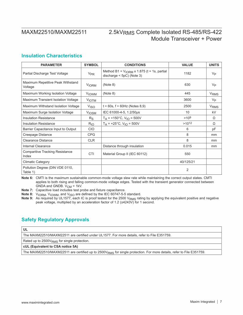
PARAMETER SYMBOL CONDITIONS VALUE UNITS
Partial Discharge Test Voltage VPRMethod B1 = VIORM x 1.875 (t = 1s, partial discharge < 5pC) (Note 3) 1182 VP
Maximum Repetitive Peak Withstand Voltage VIORM (Note 8) 630 VP
Maximum Working Isolation Voltage VIOWM (Note 8) 445 VRMS
Maximum Transient Isolation Voltage VIOTM 3600 VP
Maximum Withstand Isolation Voltage VISO t = 60s, f = 60Hz (Notes 8,9) 2500 VRMS
Maximum Surge Isolation Voltage VIOSM IEC 61000-4-5, 1.2/50μs 10 kVInsulation Resistance RS TA = +150°C, VIO = 500V >109 ΩInsulation Resistance RIO TA = +25°C, VIO = 500V >1012 ΩBarrier Capacitance Input to Output CIO 6 pFCreepage Distance CPG 8 mmClearance Distance CLR 8 mmInternal Clearance Distance through insulation 0.015 mmComparitive Tracking Resistance Index CTI Material Group II (IEC 60112) 550
Climatic Category 40/125/21
Pollution Degree (DIN VDE 0110, Table 1) 2
www.maximintegrated.com Maxim Integrated 7
MAXM22510/MAXM22511 2.5kVRMS Complete Isolated RS-485/RS-422 Module Transceiver + Power
Insulation Characteristics
Safety Regulatory Approvals
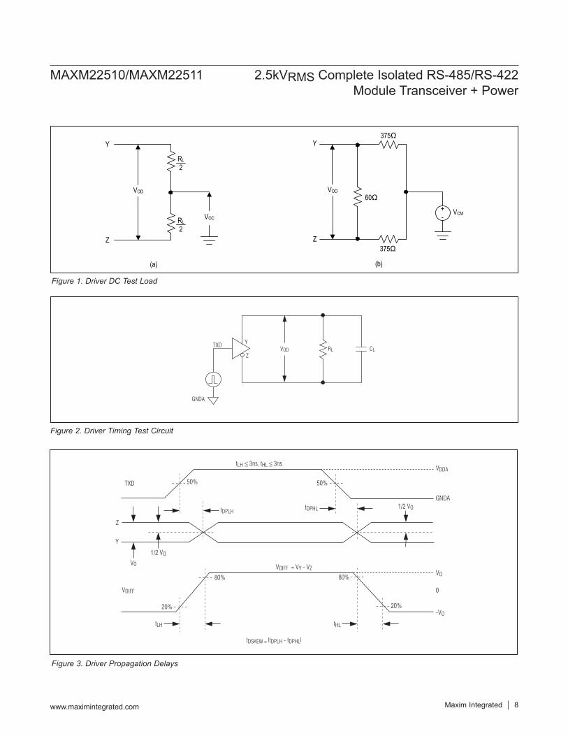
Figure 1. Driver DC Test Load
Figure 2. Driver Timing Test Circuit
Figure 3. Driver Propagation Delays
www.maximintegrated.com Maxim Integrated 8
MAXM22510/MAXM22511 2.5kVRMS Complete Isolated RS-485/RS-422 Module Transceiver + Power
RL
2
RL
2
VOC
VOD
Y
Z
(a)
375Ω
VCM
Y
Z
(b)
375Ω
+-
60ΩVOD
RL CLVODTXD
GNDA
Y
Z
50% 50%
GNDA
TXD
Z
Y
20%
80%
20%
80%
0
VO
-VO
VDIFF
tDSKEW = |tDPLH - tDPHL|
VDIFF = VY - VZ
VDDA tLH P 3ns, tHL P 3ns
1/2 VO tDPLH
tLH tHL
tDPHL
VO
1/2 VO
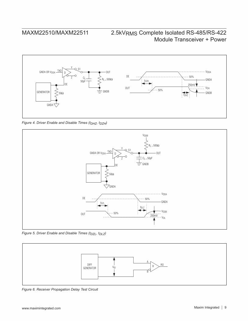
Figure 4. Driver Enable and Disable Times (tDHZ, tDZH)
Figure 5. Driver Enable and Disable Times (tDZL, tDLZ)
Figure 6. Receiver Propagation Delay Test Circuit
www.maximintegrated.com Maxim Integrated 9
MAXM22510/MAXM22511 2.5kVRMS Complete Isolated RS-485/RS-422 Module Transceiver + Power
GNDA
GNDB
250mV
50%
tDZH
tDHZ
DE
VDDA
VOH
50%
OUT
RL = 500I
50I
OUTS1Y
Z
DTXDGNDA OR VDDA
GNDA
GNDBGENERATOR
DE
CL 50pF
RL = 500I
CL = 50pF
50I
GNDB
GNDA
OUT
GNDA
250mV50%
tDZL
tDLZ
DE
S1Y
Z
DTXDGNDA OR VDDA
VDDB
VDDA
50%
OUTVDDB
VOL
GENERATOR
DE
VID
B
ARODIFF
GENERATORR
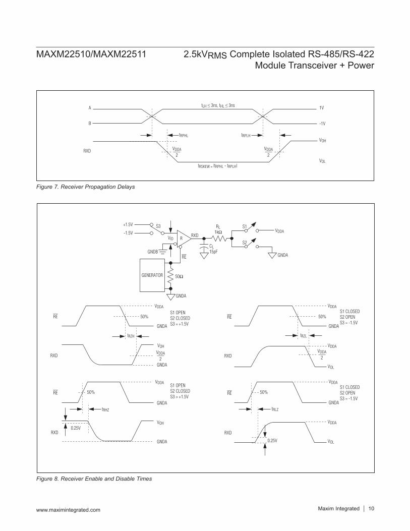
Figure 7. Receiver Propagation Delays
Figure 8. Receiver Enable and Disable Times
www.maximintegrated.com Maxim Integrated 10
MAXM22510/MAXM22511 2.5kVRMS Complete Isolated RS-485/RS-422 Module Transceiver + Power
A
B
VOH
VOL
RXD
tRPHL
tRSKEW = |tRPHL - tRPLH|
tLH P 3ns, tHL P 3ns
tRPLH
-1V
1V
2VDDA
2VDDA
GENERATOR 50I
RL1kI
CL15pF
R-1.5V
+1.5V
RXD
S1VDDA
GNDAGNDB
GNDA
S2
S3
VID
RE
RE
RXD
RE
RXD
RE RE
RXD RXD
GNDA
tRHZ tRLZ
0.25V
0.25V
50% 50%
GNDA GNDA
2
S1 OPENS2 CLOSEDS3 = +1.5V
S1 OPENS2 CLOSEDS3 = +1.5V
S1 CLOSEDS2 OPENS3 = -1.5V
S1 CLOSEDS2 OPENS3 = -1.5V
VOH
GNDA
GNDA
VOH
VDDA
VDDAVDDA
50%50%
VDDA
tRZL
VOL
GNDA
VDDAVDDA
VDDA
VOL
tRZH
2VDDA
(VDDA – VGNDA = 3.3V, VGNDA = VGNDB, and TA = +25°C, unless otherwise noted.)
Maxim Integrated 11www.maximintegrated.com
MAXM22510/MAXM22511 2.5kVRMS Complete Isolated RS-485/RS-422 Module Transceiver + Power
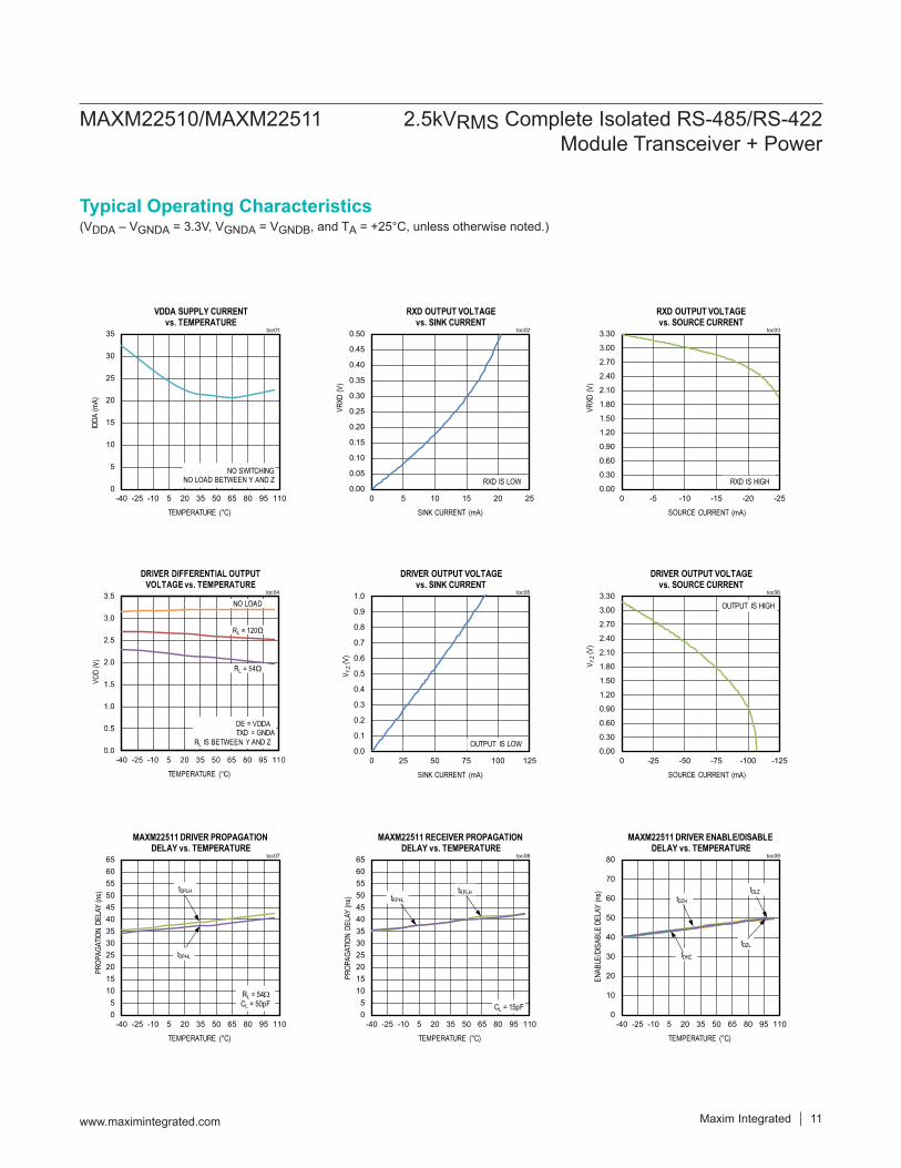
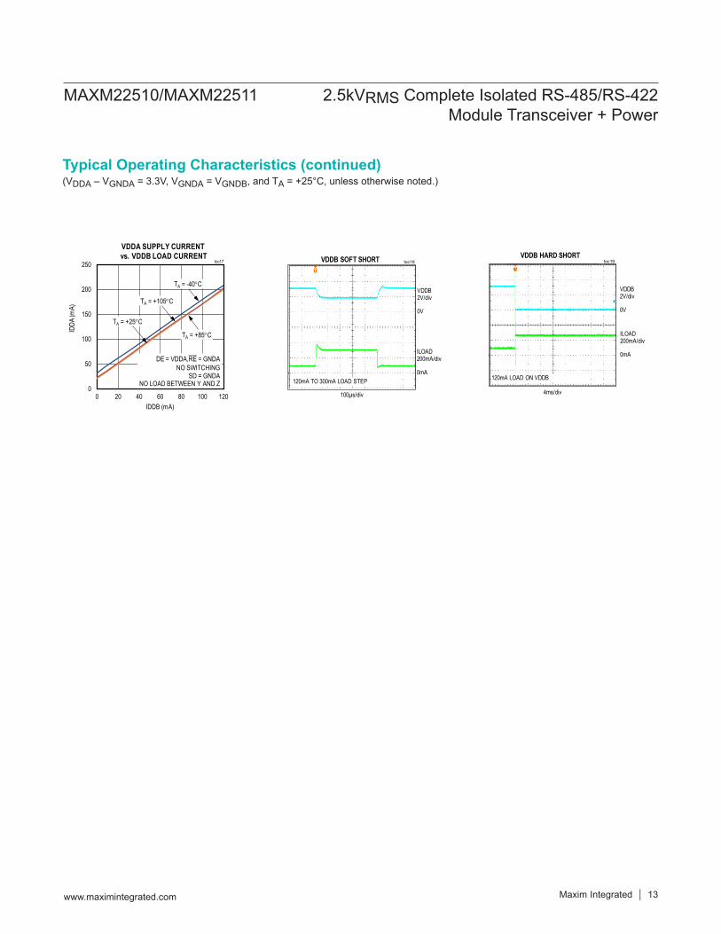
Typical Operating Characteristics
0
5
10
15
20
25
30
35
-40 -25 -10 5 20 35 50 65 80 95 110
IDDA
(mA)
TEMPERATURE (°C)
VDDA SUPPLY CURRENTvs. TEMPERATURE
toc01
NO SWITCHINGNO LOAD BETWEEN Y AND Z
05
101520253035404550556065
-40 -25 -10 5 20 35 50 65 80 95 110
PRO
PAG
ATIO
N DE
LAY
(ns)
TEMPERATURE (°C)
MAXM22511 DRIVER PROPAGATION DELAY vs. TEMPERATURE
toc07
RL = 54ΩCL = 50pF
tDPLH
tDPHL
0.00
0.05
0.10
0.15
0.20
0.25
0.30
0.35
0.40
0.45
0.50
0 5 10 15 20 25
VRXD
(V)
SINK CURRENT (mA)
RXD OUTPUT VOLTAGEvs. SINK CURRENT
toc02
RXD IS LOW
05
101520253035404550556065
-40 -25 -10 5 20 35 50 65 80 95 110
PRO
PAG
ATIO
N DE
LAY
(ns)
TEMPERATURE (°C)
MAXM22511 RECEIVER PROPAGATION DELAY vs. TEMPERATURE
toc08
tRPLHtRPHL
CL = 15pF
0.00
0.30
0.60
0.90
1.20
1.50
1.80
2.10
2.40
2.70
3.00
3.30
-25-20-15-10-50
VRXD
(V)
SOURCE CURRENT (mA)
RXD OUTPUT VOLTAGEvs. SOURCE CURRENT
toc03
RXD IS HIGH
0
10
20
30
40
50
60
70
80
-40 -25 -10 5 20 35 50 65 80 95 110
ENAB
LE/D
ISAB
LE D
ELAY
(ns)
TEMPERATURE (°C)
MAXM22511 DRIVER ENABLE/DISABLE DELAY vs. TEMPERATURE
toc09
tDHZ
tDZH
tDLZ
tDZL
0.0
0.1
0.2
0.3
0.4
0.5
0.6
0.7
0.8
0.9
1.0
0 25 50 75 100 125
V Y,Z
(V)
SINK CURRENT (mA)
DRIVER OUTPUT VOLTAGEvs. SINK CURRENT
toc05
OUTPUT IS LOW0.00
0.30
0.60
0.90
1.20
1.50
1.80
2.10
2.40
2.70
3.00
3.30
-125-100-75-50-250
V Y,Z
(V)
SOURCE CURRENT (mA)
DRIVER OUTPUT VOLTAGEvs. SOURCE CURRENT
toc06
OUTPUT IS HIGH
(VDDA – VGNDA = 3.3V, VGNDA = VGNDB, and TA = +25°C, unless otherwise noted.)
Maxim Integrated 12www.maximintegrated.com
MAXM22510/MAXM22511 2.5kVRMS Complete Isolated RS-485/RS-422 Module Transceiver + Power
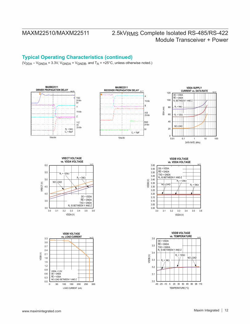
Typical Operating Characteristics (continued)
3.0
3.1
3.2
3.3
3.4
3.5
3.6
-40 -25 -10 5 20 35 50 65 80 95 110
VDD
B (V
)
TEMPERATURE (°C)
VDDB VOLTAGEvs. TEMPERATURE toc16
DE = VDDARE = GNDATXD = GNDARL IS BETWEEN Y AND Z
NO LOADRL = 120Ω
RL = 54Ω
3.0
3.5
4.0
4.5
5.0
5.5
6.0
3.0 3.1 3.2 3.3 3.4 3.5 3.6
VREC
T (V
)
VDDA (V)
VRECT VOLTAGE vs. VDDA VOLTAGE
toc13
NO LOAD
RL = 54Ω
DE = VDDARE = GNDA
TXD = GNDARL IS BETWEEN Y AND Z
RL = 120Ω
0.0
0.3
0.6
0.9
1.2
1.5
1.8
2.1
2.4
2.7
3.0
3.3
0 50 100 150 200 250 300
VDDB
(V)
LOAD CURRENT (mA)
VDDB VOLTAGE vs. LOAD CURRENT toc15
VDDA = 3.3VDE = GNDARE = VDDANO LOAD BETWEEN Y AND Z
A
1V/div
B
A-B2V/div
RXD2V/div
0V
toc11
10ns/div
CL = 15pF
MAXM22511RECEIVER PROPAGATION DELAY
3.00
3.05
3.10
3.15
3.20
3.25
3.30
3.35
3.40
3.45
3.50
3.55
3.60
3.0 3.1 3.2 3.3 3.4 3.5 3.6
VDD
B (V
)
VDDA (V)
VDDB VOLTAGE vs. VDDA VOLTAGE
toc14
NO LOAD
DE = VDDARE = GNDATXD = GNDARL IS BETWEEN Y AND Z
RL = 54Ω
RL = 120Ω
TXD2V/div0V
Y
1V/div
Z
Y-Z0V2V/div
toc10
10ns/div
RL = 54ΩCL = 50pF
MAXM22511 DRIVER PROPAGATION DELAY
0
20
40
60
80
100
120
0.01 0.1 1 10 100
IDDA
(mA)
DATA RATE (MHz)
VDDA SUPPLY CURRENT vs. DATA RATE toc12
DE = VDDARE = GNDARL BETWEEN Y AND Z
NO LOAD
RL = 54Ω
RL = 120Ω
(VDDA – VGNDA = 3.3V, VGNDA = VGNDB, and TA = +25°C, unless otherwise noted.)
Maxim Integrated 13www.maximintegrated.com
MAXM22510/MAXM22511 2.5kVRMS Complete Isolated RS-485/RS-422 Module Transceiver + Power
Typical Operating Characteristics (continued)
VDDB2V/div
0V
ILOAD200mA/div
0mA
toc18
100µs/div
VDDB SOFT SHORT
120mA TO 300mA LOAD STEP
VDDB2V/div
0V
ILOAD200mA/div
0mA
toc19
4ms/div
VDDB HARD SHORT
120mA LOAD ON VDDB
0
50
100
150
200
250
0 20 40 60 80 100 120
IDD
A (m
A)
IDDB (mA)
VDDA SUPPLY CURRENT vs. VDDB LOAD CURRENT
toc17
TA = -40°C
TA = +25°C
TA = +105°C
DE = VDDA,RE = GNDANO SWITCHING
SD = GNDANO LOAD BETWEEN Y AND Z
TA = +85°C
www.maximintegrated.com Maxim Integrated 14
MAXM22510/MAXM22511 2.5kVRMS Complete Isolated RS-485/RS-422 Module Transceiver + Power
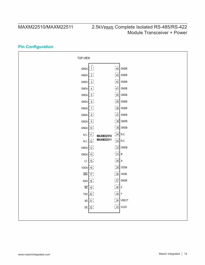
Pin Configuration
GNDB
GNDBGNDA
1
2
44
43
GNDB
GNDBGNDA
GNDA
GNDA
TOP VIEW
3
4
42
41
GNDB
GNDBGNDA
5 40 GNDBGNDA
GNDA 6
7
39
38
GNDBGNDA 8 37
MAXM22510MAXM22511
+
9
10GNDA
GNDA
11
12
I.C.
13GNDA
GNDA 14
15
VDDA 16
RE
17SBA
RXD 18
19
DE
20TXD
SD 21
22
36
35
GNDB
GNDB
34
33
B
A
32 GNDB
31
30
VDDB29
Z
Y
28
27
VDDB
GNDB
26
25
VLDO
24 VRECT
23
N.C.
N.C. N.C.
N.C.
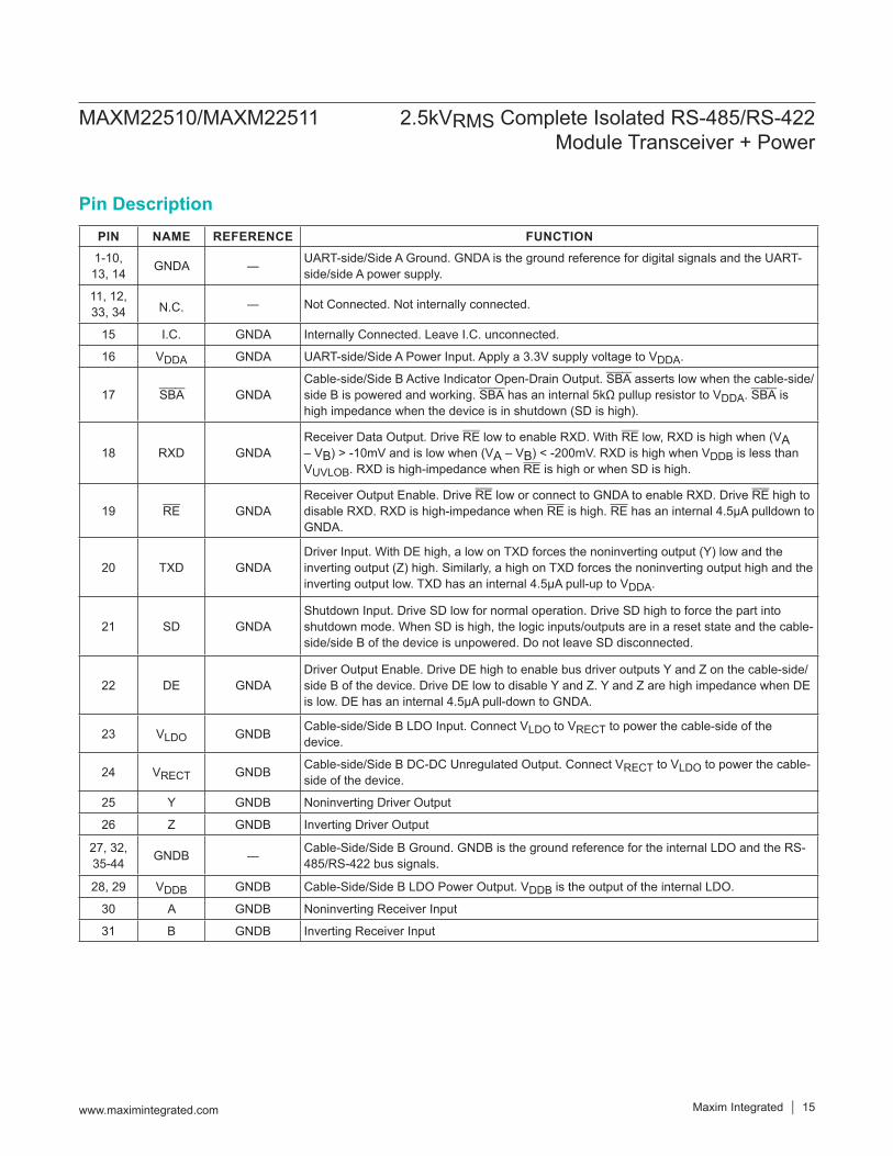
PIN NAME REFERENCE FUNCTION1-10,13, 14 GNDA ― UART-side/Side A Ground. GNDA is the ground reference for digital signals and the UART-
side/side A power supply.
11, 12, 33, 34 N.C. ― Not Connected. Not internally connected.
15 I.C. GNDA Internally Connected. Leave I.C. unconnected.
16 VDDA GNDA UART-side/Side A Power Input. Apply a 3.3V supply voltage to VDDA.
17 SBA GNDACable-side/Side B Active Indicator Open-Drain Output. SBA asserts low when the cable-side/side B is powered and working. SBA has an internal 5kΩ pullup resistor to VDDA. SBA is high impedance when the device is in shutdown (SD is high).
18 RXD GNDAReceiver Data Output. Drive RE low to enable RXD. With RE low, RXD is high when (VA – VB) > -10mV and is low when (VA – VB) < -200mV. RXD is high when VDDB is less than VUVLOB. RXD is high-impedance when RE is high or when SD is high.
19 RE GNDAReceiver Output Enable. Drive RE low or connect to GNDA to enable RXD. Drive RE high to disable RXD. RXD is high-impedance when RE is high. RE has an internal 4.5µA pulldown to GNDA.
20 TXD GNDADriver Input. With DE high, a low on TXD forces the noninverting output (Y) low and the inverting output (Z) high. Similarly, a high on TXD forces the noninverting output high and the inverting output low. TXD has an internal 4.5µA pull-up to VDDA.
21 SD GNDAShutdown Input. Drive SD low for normal operation. Drive SD high to force the part into shutdown mode. When SD is high, the logic inputs/outputs are in a reset state and the cable-side/side B of the device is unpowered. Do not leave SD disconnected.
22 DE GNDADriver Output Enable. Drive DE high to enable bus driver outputs Y and Z on the cable-side/side B of the device. Drive DE low to disable Y and Z. Y and Z are high impedance when DE is low. DE has an internal 4.5µA pull-down to GNDA.
23 VLDO GNDB Cable-side/Side B LDO Input. Connect VLDO to VRECT to power the cable-side of the device.
24 VRECT GNDB Cable-side/Side B DC-DC Unregulated Output. Connect VRECT to VLDO to power the cable-side of the device.
25 Y GNDB Noninverting Driver Output
26 Z GNDB Inverting Driver Output
27, 32, 35-44 GNDB ― Cable-Side/Side B Ground. GNDB is the ground reference for the internal LDO and the RS-
485/RS-422 bus signals.
28, 29 VDDB GNDB Cable-Side/Side B LDO Power Output. VDDB is the output of the internal LDO.
30 A GNDB Noninverting Receiver Input
31 B GNDB Inverting Receiver Input
www.maximintegrated.com Maxim Integrated 15
MAXM22510/MAXM22511 2.5kVRMS Complete Isolated RS-485/RS-422 Module Transceiver + Power
Pin Description
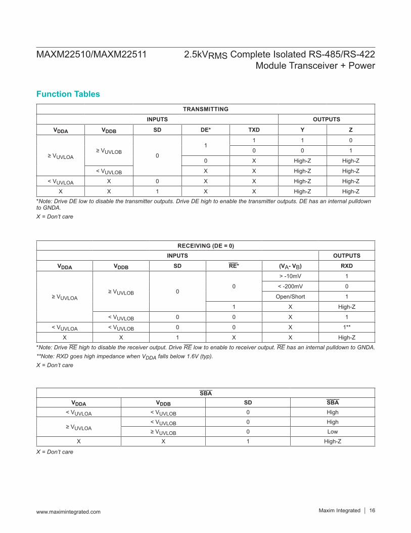
*Note: Drive DE low to disable the transmitter outputs. Drive DE high to enable the transmitter outputs. DE has an internal pulldown to GNDA.X = Don’t care
*Note: Drive RE high to disable the receiver output. Drive RE low to enable to receiver output. RE has an internal pulldown to GNDA.**Note: RXD goes high impedance when VDDA falls below 1.6V (typ).X = Don’t care
X = Don’t care
Function TablesTRANSMITTING
INPUTS OUTPUTS
VDDA VDDB SD DE* TXD Y Z
≥ VUVLOA≥ VUVLOB 0
11 1 0
0 0 1
0 X High-Z High-Z
< VUVLOB X X High-Z High-Z
< VUVLOA X 0 X X High-Z High-Z
X X 1 X X High-Z High-Z
RECEIVING (DE = 0)INPUTS OUTPUTS
VDDA VDDB SD RE* (VA- VB) RXD
≥ VUVLOA≥ VUVLOB 0
0
> -10mV 1
< -200mV 0
Open/Short 1
1 X High-Z
< VUVLOB 0 0 X 1
< VUVLOA < VUVLOB 0 0 X 1**
X X 1 X X High-Z
SBAVDDA VDDB SD SBA
< VUVLOA < VUVLOB 0 High
≥ VUVLOA< VUVLOB 0 High≥ VUVLOB 0 Low
X X 1 High-Z
www.maximintegrated.com Maxim Integrated 16
MAXM22510/MAXM22511 2.5kVRMS Complete Isolated RS-485/RS-422 Module Transceiver + Power
Detailed DescriptionThe MAXM22510/MAXM22511 isolated RS-485/RS-422 full-duplex transceiver modules provide 2500VRMS (60s) of galvanic isolation between the RS-485/RS-422 cable-side of the transceiver and the UART-side. These integrated modules require no external components and no external isolated power supply for the cable-side.These transceivers allow up to 500kbps (MAXM22510) or 25Mbps (MAXM22511) communication across an isola-tion barrier when a large potential exists between grounds on each side of the barrier.
Data Isolation Data isolation is achieved using high-voltage capacitors that allow data transmission between the UART-side and the RS-485/RS-422 cable-side of the transceiver.
Integrated DC-DC for Isolated PowerPower isolation is achieved with an integrated DC-DC and LDO. A single 3.3V supply on the UART-side of the device is used to generate a regulated 3.3V supply for the cable-side.The internal transformer used to transfer isolated power in the MAXM22510/MAXM22511 is based on a ferrite core to help reduce unwanted EMI emissions.No power is transferred from the UART-side to the cable-side when the shutdown pin (SD) is high.
True Fail-SafeThe devices guarantee a logic-high on the receiver output when the receiver inputs are shorted or open, or when connected to a terminated transmission line with all drivers disabled. The receiver threshold is fixed between
-10mV and -200mV. If the differential receiver input voltage (VA – VB) is greater than or equal to -10mV, RXD is logic-high. In the case of a terminated bus with all transmitters
disabled, the receiver’s differential input voltage is pulled to zero by the termination resistors. Due to the receiver threshold of the devices, this results in a logic-high at RXD.
Driver Output ProtectionTwo mechanisms prevent excessive output current and power dissipation caused by faults or bus contention. The first, a current limit on the output stage, provides immediate protection against short circuits over the entire common-mode voltage range. The second, a thermal- shutdown circuit, forces the driver outputs into a high-impedance state if the die temperature exceeds +160°C (typ).
Thermal ShutdownThe devices are protected from overtemperature damage by integrated thermal-shutdown circuitry. When the junction temperature (TJ) exceeds +160°C (typ), the driver outputs and RXD are high-impedance, and VDDB falls to 0V. The device resumes normal operation when TJ falls below +145°C (typ).
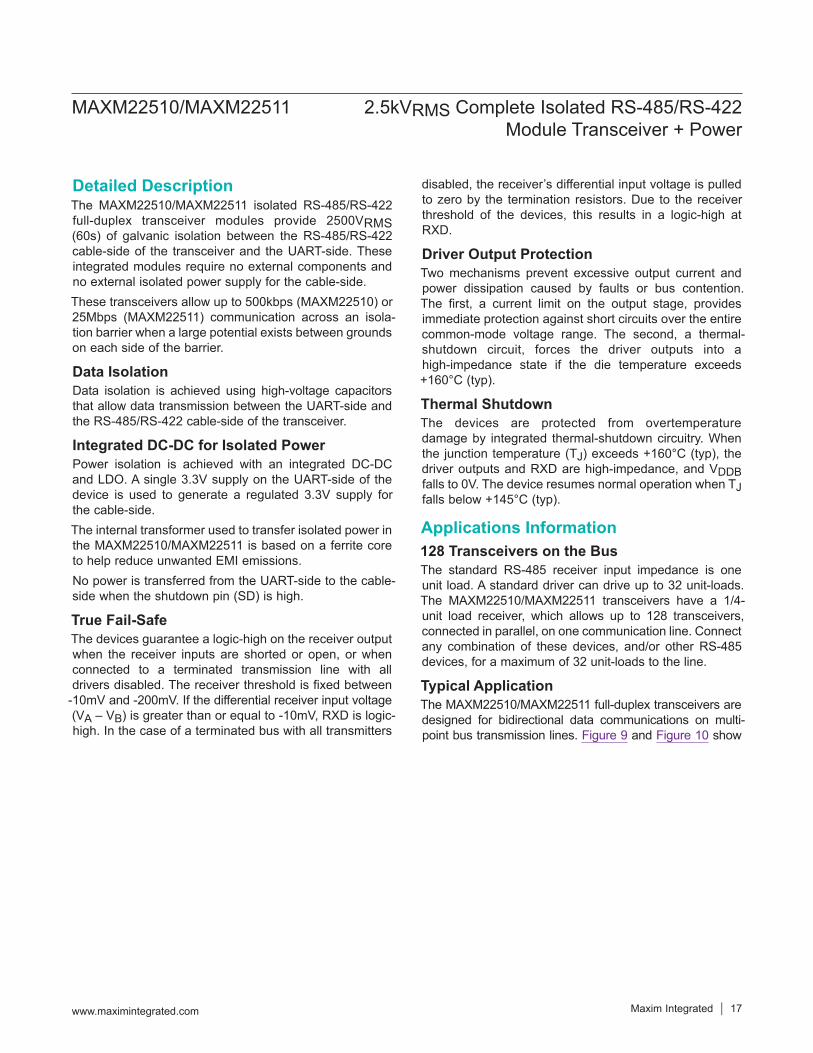
Applications Information128 Transceivers on the BusThe standard RS-485 receiver input impedance is one unit load. A standard driver can drive up to 32 unit-loads. The MAXM22510/MAXM22511 transceivers have a 1/4-unit load receiver, which allows up to 128 transceivers, connected in parallel, on one communication line. Connect any combination of these devices, and/or other RS-485 devices, for a maximum of 32 unit-loads to the line.
Typical ApplicationThe MAXM22510/MAXM22511 full-duplex transceivers are designed for bidirectional data communications on multi-point bus transmission lines. Figure 9 and Figure 10 show
www.maximintegrated.com Maxim Integrated 17
MAXM22510/MAXM22511 2.5kVRMS Complete Isolated RS-485/RS-422 Module Transceiver + Power
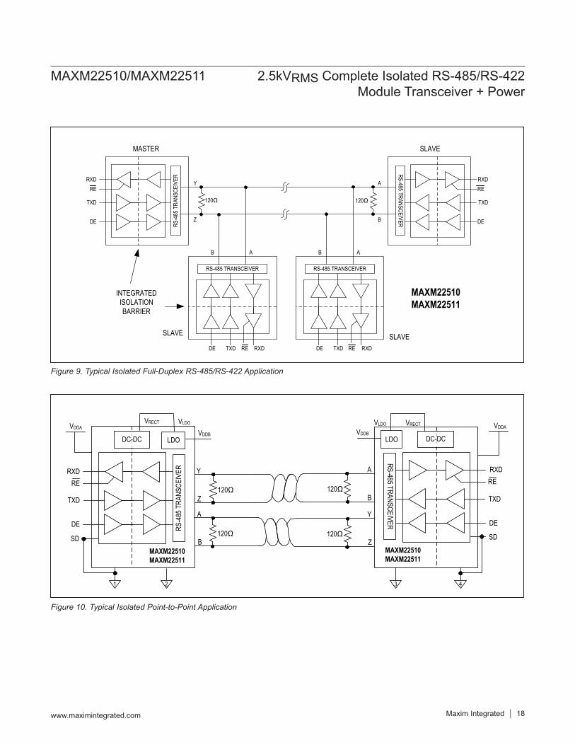
Figure 9. Typical Isolated Full-Duplex RS-485/RS-422 Application
Figure 10. Typical Isolated Point-to-Point Application
www.maximintegrated.com Maxim Integrated 18
MAXM22510/MAXM22511 2.5kVRMS Complete Isolated RS-485/RS-422 Module Transceiver + Power
RXD
RE
TXD
DE
RS-
485
TRAN
SCEI
VER
Y
Z
RXD
RE
TXD
DE
RS-485 TR
ANSC
EIVERA
B
RXDRETXDDE
RS-485 TRANSCEIVER
AB
RXDRETXDDE
RS-485 TRANSCEIVER
AB
120Ω
INTEGRATED ISOLATION BARRIER
MAXM22510MAXM22511
MASTER SLAVE
SLAVESLAVE
120Ω
RXD
RE
TXD
DE
RS-
485
TRAN
SCEI
VER Y
Z
MAXM22510MAXM22511
VLDO
VDDB
VDDA
1 2
LDO
RXD
RE
TXD
DE
RS-485 TR
ANSC
EIVER
A
B
VDDB
VDDA
3 4
VLDO
MAXM22510MAXM22511
LDO
120Ω
120Ω
A
B
Y
Z
120Ω
120Ω
DC-DC
VRECT
DC-DC
VRECT
SD SD
typical network application circuits. To minimize reflections, the bus should be terminated at both ends in its characteristics impedance, and stub lengths off the main line should be kept as short as possible.
Layout ConsiderationsIt is recommended to design an isolation, or “keep-out,” channel underneath the isolator that is free from ground and signal planes. Any galvanic or metallic connection between the cable-side and UART-side will defeat the isolation.Route important signal lines close to the ground plane to minimize possible external influences. On the cable-side of the devices, it is good practice to have the bus connectors and termination resistor as close as possible to the I/O pins.
Extended ESD ProtectionESD protection structures are incorporated on all pins to protect against electrostatic discharge encountered during handling and assembly. The driver outputs and receiver inputs of the devices have extra protection against static electricity to the cable-side ground reference. The ESD structures withstand high-ESD events during normal operation and when powered down. After an ESD event, the devices keep working without latch-up or damage.Optionally, place a 330pF Y capacitor between GNDA and GNDB for improved cable-side to UART-side ESD protection.ESD protection can be tested in various ways. The transmitter outputs and receiver inputs of the MAXM22510/MAXM22511 are characterized for protection to the cable-side ground (GNDB) to the following limits: ±35kV HBM ±18kV using the Air-Gap Discharge method specified
in IEC 61000-4-2 ±8kV using the Contact Discharge method specified
in IEC 61000-4-2
ESD Test ConditionsESD performance depends on a variety of conditions. Contact Maxim for a reliability report that documents test setup, test methodology, and test results.
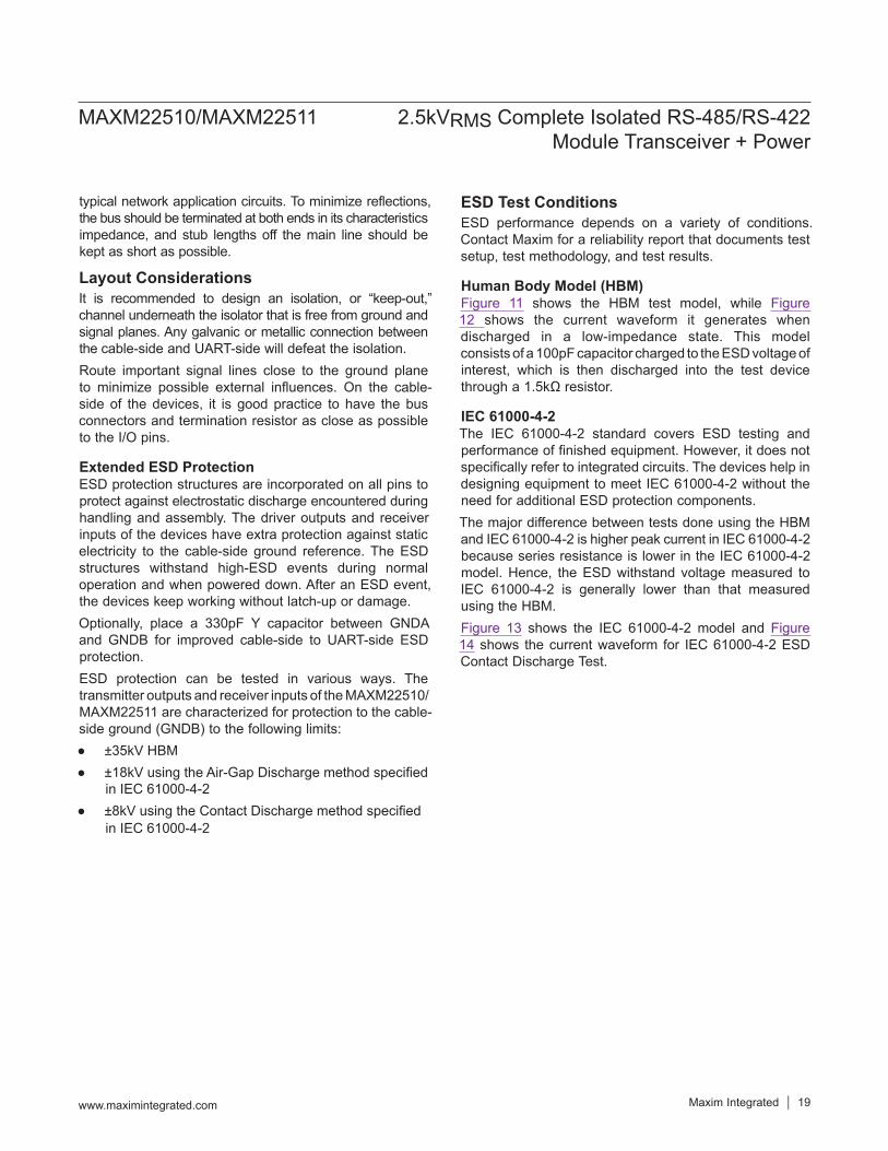
Human Body Model (HBM)Figure 11 shows the HBM test model, while Figure 12 shows the current waveform it generates when discharged in a low-impedance state. This model consists of a 100pF capacitor charged to the ESD voltage of interest, which is then discharged into the test device through a 1.5kΩ resistor.
IEC 61000-4-2The IEC 61000-4-2 standard covers ESD testing and performance of finished equipment. However, it does not specifically refer to integrated circuits. The devices help in designing equipment to meet IEC 61000-4-2 without the need for additional ESD protection components. The major difference between tests done using the HBM and IEC 61000-4-2 is higher peak current in IEC 61000-4-2 because series resistance is lower in the IEC 61000-4-2 model. Hence, the ESD withstand voltage measured to IEC 61000-4-2 is generally lower than that measured using the HBM. Figure 13 shows the IEC 61000-4-2 model and Figure 14 shows the current waveform for IEC 61000-4-2 ESD Contact Discharge Test.
www.maximintegrated.com Maxim Integrated 19
MAXM22510/MAXM22511 2.5kVRMS Complete Isolated RS-485/RS-422 Module Transceiver + Power
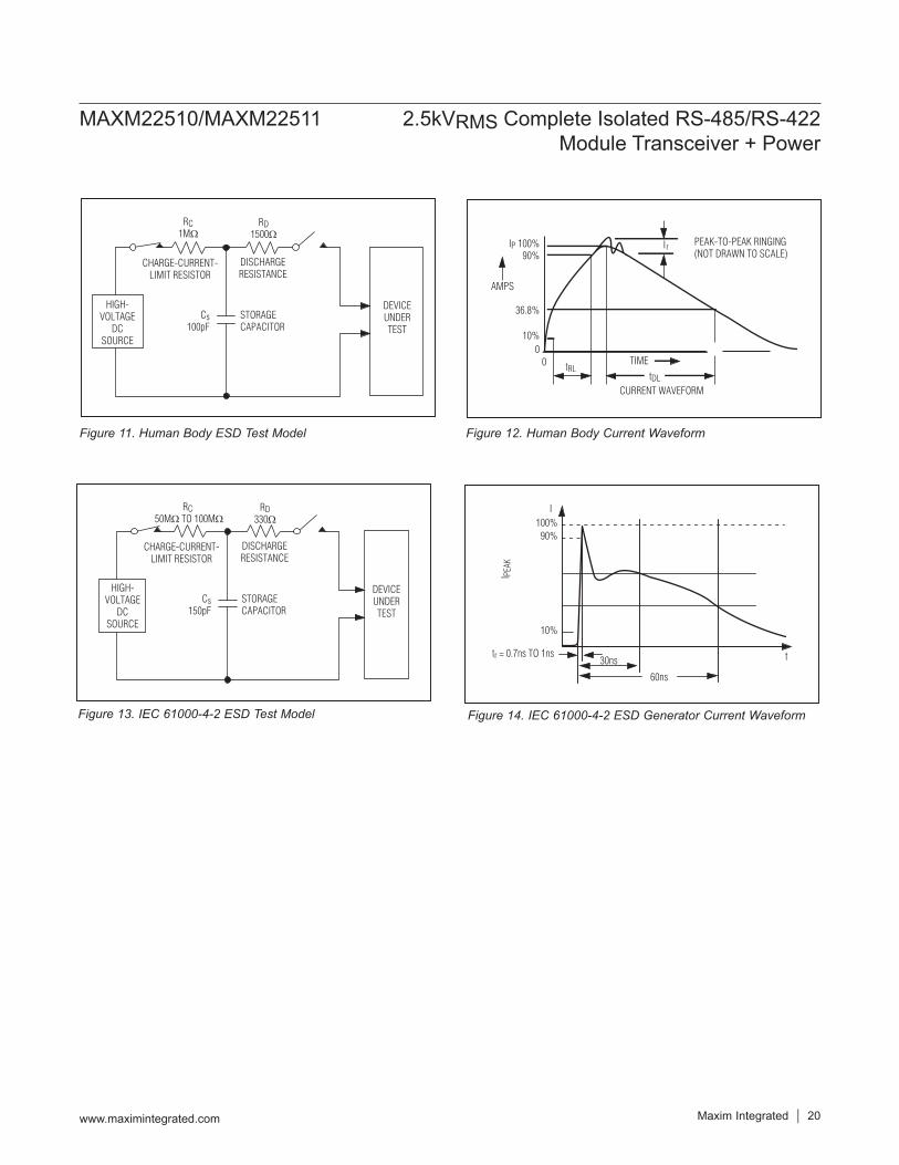
Figure 11. Human Body ESD Test Model Figure 12. Human Body Current Waveform
Figure 13. IEC 61000-4-2 ESD Test Model Figure 14. IEC 61000-4-2 ESD Generator Current Waveform
www.maximintegrated.com Maxim Integrated 20
MAXM22510/MAXM22511 2.5kVRMS Complete Isolated RS-485/RS-422 Module Transceiver + Power
CHARGE-CURRENT-LIMIT RESISTOR
DISCHARGERESISTANCE
STORAGECAPACITOR
Cs100pF
RC1MΩ
RD1500Ω
HIGH-VOLTAGE
DCSOURCE
DEVICEUNDERTEST
CHARGE-CURRENT-LIMIT RESISTOR
DISCHARGERESISTANCE
STORAGECAPACITOR
Cs150pF
RC 50MΩ TO 100MΩ
RD330Ω
HIGH-VOLTAGE
DCSOURCE
DEVICEUNDERTEST
IP 100%90%
36.8%
tRLTIME
tDL
CURRENT WAVEFORM
PEAK-TO-PEAK RINGING(NOT DRAWN TO SCALE)
Ir
10%0
0
AMPS
tr = 0.7ns TO 1ns30ns
60ns
t
100%90%
10%
I PEA
KI
www.maximintegrated.com Maxim Integrated 21
MAXM22510/MAXM22511 2.5kVRMS Complete Isolated RS-485/RS-422 Module Transceiver + Power
LDO
RS-
485
TRAN
SCEI
VER
VDDA
RXD
TXD
DE
A
B
VDDB
VRECT
GNDA GNDBMAXM22510MAXM22511
RE
ISOLATION BARRIER
uC
Z
Y
SBA
DC-DC
VLDO
SD
FULL DUPLEX CONFIGURATION
GPIO
GPIO
RXD
GPIO
GPIO
TXD
Typical Application Circuits
LDO
RS-
485
TRAN
SCEI
VER
VDDA
RXD
TXD
DE
A
B
VDDB
VRECT
GNDA GNDBMAXM22510MAXM22511
RE
ISOLATION BARRIER
uC
Z
Y
SBA
DC-DC
VLDO
SD
HALF DUPLEX CONFIGURATION
GPIO
GPIO
RXD
GPIO
TXD
GPIO
Ordering InformationPART TEMP RANGE PIN-PACKAGE
MAXM22510GLH+ -40°C to +105°C 44 LGA
MAXM22510GLH+T -40°C to +105°C 44 LGAMAXM22511GLH+ -40°C to +105°C 44 LGAMAXM22511GLH+T -40°C to +105°C 44 LGA
+Denotes a lead(Pb)-free/RoHS-compliant package. T = Tape and reel.
www.maximintegrated.com Maxim Integrated 22
MAXM22510/MAXM22511 2.5kVRMS Complete Isolated RS-485/RS-422 Module Transceiver + Power
Chip InformationPROCESS: BiCMOS
Revision HistoryREVISIONNUMBER
REVISIONDATE DESCRIPTION PAGES
CHANGED
0 6/18 Initial release —
1 7/18Updated General Description, Benefits and Features, Package Thermal Characteristics, Electrical Characteristics table, Typical Operating Characteristics, Pin Description, Function Tables, and Detailed Description
1, 2, 4–6, 11–13, 15, 16, 17, 19
1.1 Corrected typos 1, 5–6, 16, 17
2 6/19Updated the Safety Regulatory Approvals and Absolute Maximum Ratings section; added the Safety Regulatory Approvals table; updated Note 10; removed future product designation from MAXM22510GLH+ and MAXM22510GLH+T
1, 2, 7, 22
Maxim Integrated cannot assume responsibility for use of any circuitry other than circuitry entirely embodied in a Maxim Integrated product. No circuit patent licenses are implied. Maxim Integrated reserves the right to change the circuitry and specifications without notice at any time. The parametric values (min and max limits) shown in the Electrical Characteristics table are guaranteed. Other parametric values quoted in this data sheet are provided for guidance.
Maxim Integrated and the Maxim Integrated logo are trademarks of Maxim Integrated Products, Inc. © 2019 Maxim Integrated Products, Inc. 23
MAXM22510/MAXM22511 2.5kVRMS Complete Isolated RS-485/RS-422 Module Transceiver + Power
For pricing, delivery, and ordering information, please visit Maxim Integrated’s online storefront at https://www.maximintegrated.com/en/storefront/storefront.html.