Embed Size (px)
Citation preview
Characterization of Carrier Dynamics in Metal Oxide Nanostructures and
Tellurophenes
by
Benjamin Daniel Wiltshire
A thesis submitted in partial fulfillment of the requirements for the degree of
Master of Science
in
Microsystems and Nanodevices
Department of Electrical and Computer Engineering
University of Alberta
© Benjamin Daniel Wiltshire, 2017
ii
Abstract
Research was undertaken into the charge carrier dynamics of TiO2 nanotube and nanowire
structures, which have potential in many technological applications and are already used in solar
cells, OLED’s, photocatalysts, and biomedical applications. Using a combination of Time of
Flight, Photoconductivity, IV, CV, and Time Resolved Microwave Conductivity, the charge
carrier dynamics of TiO2 nanostructures were measured and later improved upon using a self-
assembled monolayer surface for passivation, with mobility improving by a factor of almost 1000.
The Time of Flight and Time Resolved Microwave Conductivity are explained in detail and can
be used quickly, easily, and with a wide variety of materials to measure important material
properties that are difficult to find using other methods.
Organic Tellurophenes were also investigated using quantitative photoluminescence (PL)
measurements such as quantum yield measurements and time resolved photoluminescence. The
Tellurophenes were previously uncharacterized and only available in small quantitites. They were
found to have unique properties such as triplet-decay leading to phosphorescent light emission
which was tunable and with a relatively high quantum yield. The Tellurophenes were also found
to have relatively high carrier mobilities after doping as high as 1.1 × 10⁻⁴𝑐𝑚2𝑉−1𝑠−1.
iii
Preface
Some of the research conducted for this thesis forms part of a research collaboration, led by
Professor Dr. Karthik Shankar and Dr. Eric Rivard at the University of Alberta. The tellurophene
material mentioned in section 1.2.3, 3.3, and 3.4 was made by Gang He. The results from section
3.3 were published as He, Gang, BD Wiltshire et al. "Phosphorescence within tellurophenes and
color tunable tellurophenes under ambient conditions." Chemical Communications 51.25 (2015):
5444-5447. A different tellurophene material from the same group was treated with iodine and
used in section 3.4 and published as Mohammadpour, Arash, BD Wiltshire, et al. "Charge
transport, doping and luminescence in solution-processed, phosphorescent, air-stable tellurophene
thin films." Organic Electronics 39 (2016): 153-162.
Results in section 3.2 is part of a collaboration between the Shankar group and the Daneshmand
group in the Electrical and Computer Engineering Department at the University of Alberta. The
microwave resonators were designed, fabricated, tested, and simulated by Mohammad Zarifi and
the Daneshmand group. The results shown in section 3.2 were published as Zarifi, M. H., et al.
"Time-resolved microwave photoconductivity (TRMC) using planar microwave resonators:
Application to the study of long-lived charge pairs in photoexcited titania nanotube arrays." The
Journal of Physical Chemistry C 119.25 (2015): 14358-14365.
Results in section 3.1 was published as Mohammadpour, Arash, et al. "Majority carrier transport
in single crystal rutile nanowire arrays." physica status solidi (RRL)-Rapid Research Letters 8.6
(2014): 512-516. and Mohammadpour, A., BD Wiltshire, et al. "100-fold improvement in carrier
drift mobilities in alkanephosphonate-passivated monocrystalline TiO2 nanowire arrays."
Nanotechnology 28.14 (2017): 144001.

iv
Acknowledgements
I would first like to thank Dr. Shankar, my supervisor, who was constantly a guiding and helping
presence in every task and challenge I faced in my work. He was an excellent source of knowledge
and advice and constantly pushed me to better myself and improve. He has taught me so much
since I was a student in his EE 250 class and I am forever grateful for his patience, kindness, and
direction over all these years.
I would also like to thank my mentors and friends in the university who helped guide my work and
taught me the ins and outs of research: Dr. Mojgan Daneshmand, Dr. Eric Rivard, Dr. Vladimir
Michaelis, Arash Mohammadpour, Samira Farsinezhad, Abdelrahman Askar, Mourad Benlamri,
Piyush Kar, Yun Zhang, Kaveh Ahadi, Ujwal Thakur, Mohammad Zarifi, Gang He, Lhing Hsuan-
Hseieh, Prashant Waghmare, Joel Boulet, Himani Sharma, Najia Mahdi, Ryan Kisslinger, Weidi
Hua, and so many more.
Thanks as well to my family and friends, who support and encourage me always in whatever I do.
Their love and patience gives me the spirit to improve myself and keep moving forward and I am
forever grateful.
v
Table of Contents
1) Introduction 1
1.1) Overview…………………………………………………………………………...1
1.2) Introduction to Titanium Dioxide Nanostructures…………………………………2
1.2.1) Introduction to Charge Transport in Nanostructured TiO2………...…… 4
1.2.2) Introduction to the Optical Properties of TiO2 Nanostructures………......6
1.3) Introduction to Charge Carrier Dynamics………………………………………….7
1.4) Introduction to Self-Assembled Monolayers and Charge Transport Applications...9
1.5) Introduction to Photoluminescence and Time Resolved Photoluminescence……...12
1.6) Introduction to Tellurophenes: Characteristics and Applications…………….……13
2) Fabrication and Experimental Methods 16
2.1) Electrochemical Anodization of TiO2 Nanotubes………………………………….16
2.2) Solvothermal Growth of TiO2 Nanowires………………………………………….19
2.3) Formation of Self Assembled Monolayers…………………………………………24
2.4) Carrier Dynamics: Characterization Methods…………………………………….. 26
2.4.1) Time of Flight Measurements………………………………………….... 26
2.4.2) Conductance, Capacitance, and Voltage Measurements…………………31
2.5) Photoluminescence, Quantum Yield, and Time Resolved Photoluminescence……34
2.5.1) Fabrication of Photoluminescent Tellurophenes…………………..……...34
2.5.2) Measuring Photoluminescence and Recognizing Unwanted Scattering….35
2.5.3) Measuring Quantum Yield for Photoluminescent Materials……………..37
2.5.4) Measuring Time-Resolved Photoluminescence………………………….39
2.6) Microwave Resonators and Microwave Characterization………………………….40
3) Experimental Results and Analysis 44
3.1) Charge Carrier Dynamics of Functionalized TiO2 Nanowires……………………..44
3.1.1) Experimental Setup……………………………………………………….44
3.1.2) Charge Carrier Dynamics of TiO2 Nanowires……………………………45
3.1.3) Charge Carrier Dynamics of Functionalized TiO2 Nanowires…………...50
3.1.4) Discussion…….…………………………………………………………..56
3.2) Characterization of TiO2 Nanostructures using Microwave Resonators…………...57
3.2.1) Experimental Setup……………………………………………………….58
3.2.2) Microwave Characterization Results……………………………………..60
3.2.3) Discussion…….…………………………………………………………..66
3.3) Measuring Phosphorescence of Tellurophenes……………….…………………….67
3.3.1) Experimental Setup…………………………………………………....….68
3.3.2) Photoluminescence of Tellurophenes………….….………………………68
3.3.3) Discussion……………………….………………………………………..75
3.4) Charge Carrier Dynamics of Tellurophenes………………………..……………….75
3.4.1) Experimental Setup……………………………………………………….76
3.4.2) Photoluminescence and Charge Transport Results……………………….77
3.4.3) Discussion……………….………………………………………………...78
4) Conclusion and Future Research Directions 80
vi
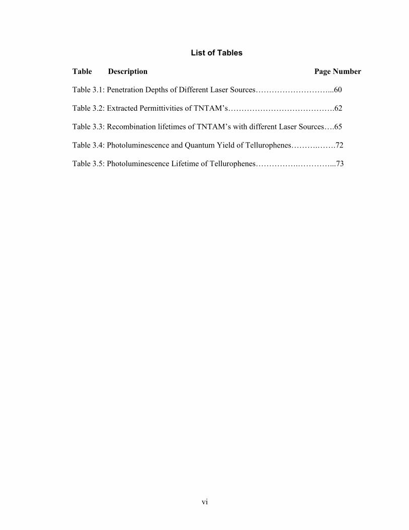
List of Tables
Table Description Page Number
Table 3.1: Penetration Depths of Different Laser Sources………………………...60
Table 3.2: Extracted Permittivities of TNTAM’s………………………………….62
Table 3.3: Recombination lifetimes of TNTAM’s with different Laser Sources….65
Table 3.4: Photoluminescence and Quantum Yield of Tellurophenes……….…….72
Table 3.5: Photoluminescence Lifetime of Tellurophenes…………….…………...73

vii
List of Figures
Figure Description Page Number
Figure 1: Anatase and Rutile crystal structures of TiO2…………………………..3
Figure 2: Rutile TiO2 Nanowires grown on an FTO slide displaying their
scattering properties……………………………………………………………….7
Figure 3: The anodization reactions that govern TiO2 nanotube growth………….17
Figure 4: The chemical structure of titanium butoxide……………………………21
Figure 5: Rutile single crystal nanowires………………………………………….23
Figure 6: XRD and UV-Vis of single crystal rutile nanowires …………………...23
Figure 7: The ODPA molecule chosen as a passivating SAM…………………….25
Figure 8: The TOF setup used in our experiments, the oscilloscope measures at
the gold contacts……………………………………………………………………27
Figure 9: A typical plot of a TOF signal showing the transient voltage and
with the transit time labelled……………………………………………………….28
Figure 10: Synthesis done by the Rivard group to create the Tellurophenes
we tested……………………………………………………………………………34
Figure 11: A microwave ring resonator, with a TiO2 membrane across the left
coupling gap………………………………………………………………………...40
Figure 12: Schematic of nanowire growth and funcitonalization for TOF on an FTO
substrate: the blank FTO substrate, nanowires grown via hydrothermal method, debris
removed from nanowires using oxygen plasma, nanowires immersed in SAM for
functionalization, metal contact thermally evaporated onto nanowires………….....45
Figure 13: illuminated and dark IV measurements showing the increased
photoconductivity under UV illumination, and the onset of SCLC at 1 V…………46
Figure 14: CV data from single crystal rutile nanowires using a voltage sweep……48
Figure 15: The TOF result of a single crystal rutile nanowire with a titanium
contact, allowing for hole conduction to also be measured…………………………49
viii
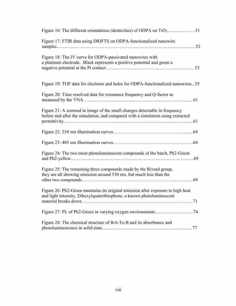
Figure 16: The different orientations (denticities) of ODPA on TiO2………………51
Figure 17: FTIR data using DRIFTS on ODPA-functionalized nanowire
samples………………………………………………………………………………52
Figure 18: The IV curve for ODPA-passivated nanowires with
a platinum electrode. Black represents a positive potential and green a
negative potential at the Pt contact……………………………………………….…53
Figure 19: TOF data for electrons and holes for ODPA-functionalized nanowires...55
Figure 20: Time resolved data for resonance frequency and Q-factor as
measured by the VNA………………………………………………………….......61
Figure 21: A zoomed in image of the small changes detectable in frequency
before and after the simulation, and compared with a simulation using extracted
permittivity…………………………………………………………………………61
Figure 22: 254 nm illumination curves………………………………………….....64
Figure 23: 405 nm illumination curves…………………………………………….64
Figure 24: The two most photoluminescent compounds of the batch, Ph2-Green
and Ph2-yellow……………………………………………………………………..69
Figure 25: The remaining three compounds made by the Rivard group,
they are all showing emission around 530 nm, but much less than the
other two compounds………………………………………………………………69
Figure 26: Ph2-Green maintains its original emission after exposure to high heat
and light intensity, Dihexylquaterthiophene, a known photoluminescent
material breaks down………………………………………………………………71
Figure 27: PL of Ph2-Green in varying oxygen environments…………………….74
Figure 28: The chemical structure of B-6-Te-B and its absorbance and
photoluminescence in solid state………………………………………………..…77
ix
List of Abbreviations
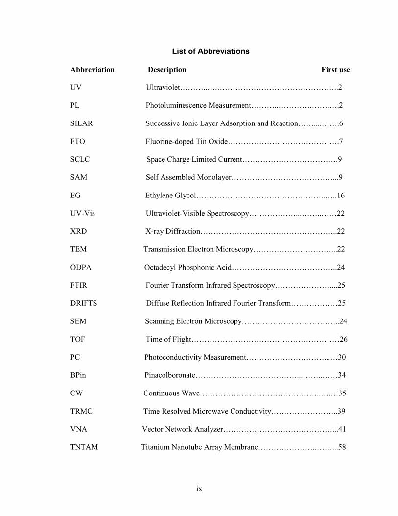
Abbreviation Description First use
UV Ultraviolet………..….………………………………………..2
PL Photoluminescence Measurement………..………….…….….2
SILAR Successive Ionic Layer Adsorption and Reaction……....…….6
FTO Fluorine-doped Tin Oxide…………………………………….7
SCLC Space Charge Limited Current……………………………….9
SAM Self Assembled Monolayer…………………………………...9
EG Ethylene Glycol…………………………………………..…..16
UV-Vis Ultraviolet-Visible Spectroscopy………………...……..……22
XRD X-ray Diffraction……………………………………………..22
TEM Transmission Electron Microscopy…………………………...22
ODPA Octadecyl Phosphonic Acid…………………………………..24
FTIR Fourier Transform Infrared Spectroscopy…………………....25
DRIFTS Diffuse Reflection Infrared Fourier Transform………………25
SEM Scanning Electron Microscopy………………………………..24
TOF Time of Flight…………………………………………………26
PC Photoconductivity Measurement…………………………...…30
BPin Pinacolboronate…………………………………...……..……34
CW Continuous Wave………………………………………..….…35
TRMC Time Resolved Microwave Conductivity……………………..39
VNA Vector Network Analyzer……………………………………...41
TNTAM Titanium Nanotube Array Membrane…………………..……...58

x
THF Tetrahydrofuran……………………………………………….68
Ph2-Green 2,5-BPin2-3,4-Ph2-Te…………………………………...……..70
Ph2-Yellow 2,4-BPin2-3,5-Ph2-Te……………………………………...…..70
PMT Photomultiplier Tube……………………………………….…72
TRDI Time Resolved Dark Injection…………………………….…..77
1
Chapter One: Introduction
1.1 Overview
It has been almost 60 years since December 29th 1959, when Richard Feynman gave his
keynote speech “There’s Plenty of Room at the Bottom”[1], introducing the ideas and
promises of nanotechnology, and how a new nanosized world was waiting to be explored
just beyond the limits of the current technology. This was a time when rockets and space
flight dominated the science headlines, and the integrated circuit had been invented the
same year but was only in its infancy. Over time though, Feynman’s forecast turned out
to be correct as nanotechnology has made a huge impact on human achievement over the
last half decade.
In the past, stone was the most useful material for tools and weapons because it was
abundant and could be made into rough shapes. Then bronze was discovered, and we found
that with heat we could make a metal alloy stronger than what we had before, and more
useful. Later, the Iron Age and then the invention of steel kept pushing humanity towards
more and more capabilities, until we had almost the entire periodic table at our disposal.
A defining feature of nanotechnology is that the properties of a material can change on
very small size scales, leading to new ideas and applications. Many of these applications
are truly unique in that only by building at such small dimensions do they become possible,
making this truly an opportunity for cutting edge research to do more with (much) less.
2
Described as the science of materials between 1 and 100 nm in dimension, nanotechnology
has become a huge field in science and engineering. The commercial applications of
nanotechnology are large and growing, with roles in food packaging[2-4], non-stick and
waterproof coatings[5-7], household appliances and clothing[8-10], sensors[11-13],
medical applications[14-16], photocatalysis and CO2 photoreduction[17-19], LED’s and
OLED’s[20-22], solar cells[23-25], and of course the transistor: the building block of all
modern digital devices. But interest in nanotechnology is not just based on what has been
done, but rather what can be done; and research in the field will likely continue for at least
another 60 years.
1.2 Introduction to Titanium Dioxide Nanostructures
Titanium dioxide is a compound with the chemical formula TiO2, it is formed naturally in
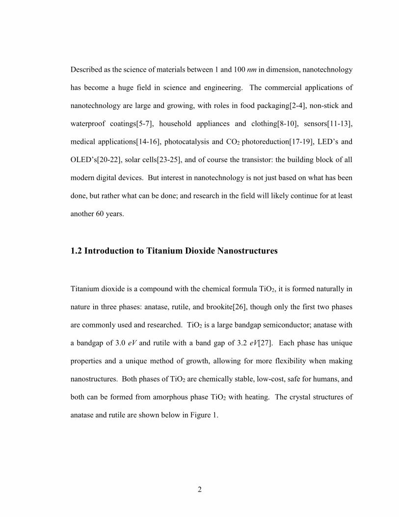
nature in three phases: anatase, rutile, and brookite[26], though only the first two phases
are commonly used and researched. TiO2 is a large bandgap semiconductor; anatase with
a bandgap of 3.0 eV and rutile with a band gap of 3.2 eV[27]. Each phase has unique
properties and a unique method of growth, allowing for more flexibility when making
nanostructures. Both phases of TiO2 are chemically stable, low-cost, safe for humans, and
both can be formed from amorphous phase TiO2 with heating. The crystal structures of
anatase and rutile are shown below in Figure 1.
3
Figure 1: Anatase (a) and Rutile (b) crystal structures of TiO2. Adapted from [28]
Titanium dioxide has been commonly used in many modern applications including
photocatalysis[6, 29], Ultraviolet (UV) sensing[30], solar cells[31, 32], LEDs/OLEDs[33],
self-cleaning surfaces[34, 35], water treatment[36, 37], and CO2 photoreduction[17, 38].
In these apications, and in addition to the two most common phases of TiO2, there are many
nanostructured forms it can be grown in including nanospheres[39-41], nanotubes[42-44],
nanowires[32, 45, 46], and nanorods[47-49]. These nanostructures are grown with a
variety of methods and steps, which include electrochemical anodization, hydrothermal or
solvothermal synthesis, high temperature annealing, sol-gel methods, porous templating,
chemical vapor deposition, and atomizing spray depositions.
As a semiconductor, TiO2 is UV sensitive, and strongly absorbs light up to about 400 nm
wavelength[50], with some absorption in the visible spectrum due to impurities or
4
dopants[51]. It is an n-type semiconductor in bulk due to the formation of oxygen
vacancies and titanium interstitial defects[52]. In nanostructures the n-type distinction is
less common because of an increasing dependence on surface defects relative to bulk
defects[53]. Despite this, it is still possible and common for TiO2 to be used as an electron
transport layer; but it makes it important to understand and study its semiconductor
properties as a nanostructure relative to the bulk material.
1.2.1 Introduction to Charge Transport in Nanostructured TiO2
Bulk TiO2 is a wide bandgap semiconductor. Due to the high permittivity and low
conductivity in undoped TiO2, titania behaves as a relaxation-type semiconductor instead
of a lifetime semiconductor[54]. The dielectric relaxation time in TiO2 is large thus causing
charge density fluctuations to persist over longer time periods than in typical
semiconductors such as Si and GaAs, and resulting in effects such as persistent
photoconductivity and space charge limited currents[55]. Another unusual attribute of
TiO2 owing partly to relaxation effects, is the wide variability over seven orders of
magnitude in charge transport parameters (i.e. electron mobility) depending on the phase,
method of synthesis, grain size, surface treatment, etc[56, 57]. The measured mobility is
also dependent on the type of technique used to make the measurement. High frequency
techniques such as time domain terahertz spectroscopy and time-resolved microwave
conductivity measure charge transport over short distances (e.g. intra-grain transport) and
may not reflect the conditions of transport most relevant to the performance of devices such
as chemiresistive sensors, solar cells or photoelectrochemical cells[56]. Low frequency
5
methods such as impedance spectroscopy[58] and intensity modulated
photocurrent/photovoltage spectroscopies[59] are more relevant to the physical conditions
present in common optoelectronic devices that use TiO2 thin films, but do not provide
explicit values for the electron mobility. Other common methods like the Hall Effect
cannot be used with conductive substrates, which TiO2 nanostructures are commonly
grown on. For these reasons, the charge dynamics of TiO2 nanostructures is not extensively
studied. The bulk mobility of single crystal anatase TiO2 is reported as 4-20 𝑐𝑚2𝑉−1𝑠−1
[60], however, the electron mobility in polycystalline nanoparticulate thin films with high
trap densities and a random walk-type transport mechanism can be as low as 10-7 cm2V-1s-
1 [61]. The bulk mobility of single crystal rutile TiO2 is about 0.1 𝑐𝑚2𝑉−1𝑠−1 [62] but can
be much lower due to the same problems.
As the dimensions of a wire or film or structure decrease, the object’s size and surfaces
begin to have a greater effect on the optical, electrical, and mechanical properties. This
can be due to a number of effects; for very small nanostructures of many materials, on the
order of 10 nm or less, quantum effects begin to occur such as tunneling or bandgap shifts.
The exciton Bohr radius of TiO2 smaller than 2 nm[63, 64]. Therefore, classic quantum
confinement effects are not seen in TiO2 nanostructures. However the increased effect of
the surface and the ambient does manifest itself in the conductivity, absorption and
luminescence of nanometer-sized TiO2. For larger size dimensions (~100 nm – 1 μm), but
not quite on the order of bulk material, different effects can occur which affect the
conductivity as well, including a relative increase of surface effects, grain sizes, charge
6
carrier path length differences, Mie scattering, and material differences due to nano- or
microfabrication.
1.2.2 Introduction to the Optical Properties of TiO2 Nanostructures
As previously mentioned, TiO2 is a large bandgap semiconductor, which makes them
useful as UV blocking agents in sunscreens or as UV detectors or sensors. Anatase has an
indirect band gap while rutile has a direct band gap where the conduction band and valence
band align over the Γ plane[28], though neither commonly exhibit strong
photoluminescence. Theory predicts the formation of 2D excitons in both anatase and
rutile. It is only extremely recently that strongly bound 2D excitons with character
intermediate between Frenkel- and Wannier- excitons have been observed in anatase single
crystals and nanoparticles[65]. Due to the large bandgap, TiO2 is mostly transparent in the
visible spectrum. This gives flexibility in the use of dyes, quantum dots, biomarkers, or
other light sensitive materials when making devices or conducting experiments – the TiO2
can often act as a scaffold for visible light sensors and photocatalysts while not absorbing
visible light itself[66, 67]. This can be incorporated with the methods of sputtering[17],
electrodeposition[68], photodeposition[69], spin or drop coating[48], or Succesive Ionic
Layer Adsorption and Reaction (SILAR)[70] to name a few.
Using the methods above, a UV sensor using TiO2, nanostructured or otherwise, can be
made into a visible light sensor, so long as the introduced material is sufficiently absorbing
7
and the charge transfer between device and detector is still high enough to be measured.
For these sensing purposes, a TiO2 scaffold also has an added benefit because TiO2
nanostructures are highly dispersive, and can increase the path length of any light passing
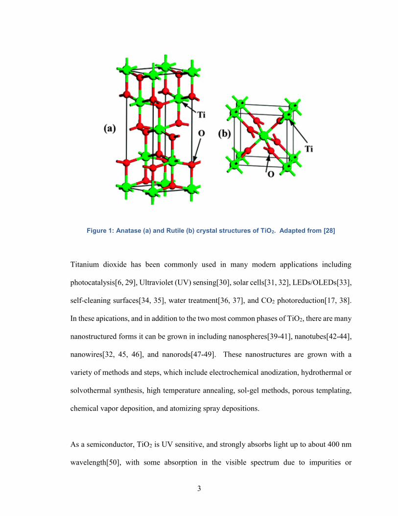
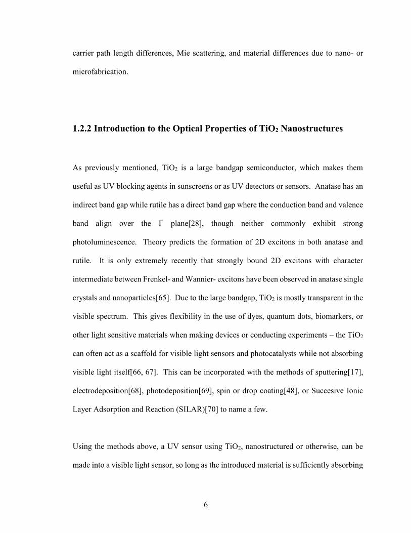
through them via reflection, refraction, and diffraction[71, 72]. This is why TiO2 nanotubes
and nanowires often appear cloudy (Figure 2) instead of completely transparent, despite no
visible light being absorbed.
Figure 2: Rutile TiO2 Nanowires (the white opaque region) grown on an FTO slide
1.3 Introduction to Charge Carrier Dynamics
One of the most important topics in modern electrical engineering is knowing how charges
move through a material or across heterojunctions. Since the arrival of the diode, charge
transport and charge transfer problems are no longer solved by linear application of Ohm’s
law. Integrated circuits, which make up a huge portion of the electronics industry, are
made of semiconductors; as are LED’s, solar cells, and many chemical and light sensors.
8
To model these semiconductors and to discover how charge moves through them, we need
to know a lot of details about the material itself; such as its crystallinity, doping
concentration, defects (density and type), and the morphology and structure of the material
itself. We also have to know about the charges moving through it, whether they are
electrons, holes, ions, or a mix; whether they were generated by injection, light, or heat;
and whether it is a strong or weak signal; or a high or low frequency signal. Due to the
large number of parameters involved, our goals in characterizing charge transport will be
simplified to dealing with TiO2 nanostructures and a test of recently synthesized
tellurophenes provided by the Rivard group in the Chemistry Department.
Most materials’ charge carrier dynamics can be approximated by a few key material
parameters. Conductivity (σ) is a measure of how much current (J) flows relative to an
applied electric field (E). Conductivity is typically viewed as a sum of electron
conductivity and hole conductivity which can in turn be broken up as the product of
mobility (μ) and the mobile charge density (n).
𝐽 = 𝜎�� (1)
𝜎 = 𝑞𝑛𝑒𝜇𝑒 + 𝑞𝑛ℎ𝜇ℎ (2)
Other considerations for measuring the current include what ‘regime’ the material is
conducting within. The Ohmic regime assumes that charge carriers are moving through
the material without accumulating in traps or reaching contact barriers. This type of
transport occurs when the excess charge carrier concentration does not exceed the
9
equilibrium or steady-state carrier concentration. For non-metallic materials, particularly
wide bandgap semiconductors and insulators, the equilibrium carrier concentration can be
quite low so that even small excess charge concentrations can be large relative to the
equilibrium carriers. When this happens, the material conducts in the space-charge limited
current (SCLC) regime[73, 74]. Essentially, the current is no longer limited by how many
equilibrium charge carriers can be moved by the electric field; the current now primarily
consists of excited or injected carriers. The main limiting factor in current flow at this
point is the space charge that forms near the source of the excess carriers, acting as a barrier
for further charges to be injected or excited[75, 76].
1.4 Introduction to Self-Assembled Monolayers and Charge Transfer
Applications
Self-Assembled Monolayers (SAMs) are common in research across many fields because
they act as extremely thin coatings which can greatly change the properties of a material
surface. They are easy to work with because they self-assemble, and the method of
preparation is often as simple as setting up a suitable environment for growth.
SAMs are of interest in research today because they can give us insights on self-
organization, surface energy modification, and they can accurately model 2D problems in
physical chemistry and statistical physics[77]. SAMs are also very useful because they
have applications in many fields; including amphiphobic coatings[78, 79], corrosion
10
protection[80, 81], biosensing and biomedical implants[82, 83], molecular sensing[84],
work function modification[85, 86], and surface adhesion[87, 88].
SAMs are also useful to improve the electrical conduction of nanostructures such as
nanotubes[79, 89], nanowires[90, 91], and nanoparticles[92]. By adsorbing to the
nanostructure surface, defects along the surface can be passivated[93]. Surface problems
such as a high defect density or Fermi level pinning can be fixed using SAMs in this way.
A lower defect density would improve current movement along the surface of the
nanostructures and reduce the rate of unwanted recombination when used in devices like
LED’s or solar cells. Removing or adjusting the effect of Fermi level pinning could also
improve surface interfaces with other electrical layers in the device by improving energy
level matching, or reduce the trap density for charge carriers at the surface, which would
also improve mobility of the materials[94, 95].
SAMs are most commonly organic molecules with two key functional groups, a head group
that will chemically adsorb to the surface, and a tail group that will give rise to the modified
surface properties[77]. The head group is chosen to strongly adhere to the desired surface,
to ensure stability of the monolayer and to speed up the adsorption process. The tail group
is often a rod-like organic molecule with two key properties. First, the tail group should
not bond to the head group to ensure that the growth stops after the first layer has covered
the surface. Second, the tail group should not be too large so that it can accommodate
close-packing of the head groups on the surface, enabling complete and uniform surface

11
coverage. A tail group that is too large will not be able to form the columnar or tilted
columnar structure that is necessary for successful self-assembly.
Due to their organic nature, SAMs must be chosen carefully so that they do not decrease
the conductivity of the device being treated. Non π-conjugated compounds are insulating.
Even π-conjugated organic molecules are generally much less conductive because they are
larger molecules that do not lose their individual identity in molecular crystals (thus
preventing the requisite delocalization of valence electrons)[96]. The low symmetry of
molecular crystals that typically arrange themselves in monoclinic or triclinic Bravais
lattices also prevents simple substitutional doping because thermodynamic and kinetic
considerations decrease the probability of an electron-donating or hole-donating foreign
molecule resulting in a shallow dopant energy level[97]. Therefore, a high carrier density
cannot be obtained as in metals; organic molecules are also rarely crystalline, or require
processing to make them crystalline – this leads to much lower mobility than their
inorganic counterparts. Organic charge transport is also typically a hopping process, as
charges must move past an energy barrier when moving from molecule to molecule[98].
This is typically a slower process than transport in crystalline inorganic materials, where
charge carriers move through the material lattice in continuous bands. As a result of these
problems with organic SAMs, it is important that charge does not transfer into the SAMs
from the nanostructures, and that the SAMs only passivate the surface.
12
1.5 Introduction to Photoluminescence and Time Resolved
Photoluminescence
The rate of spontaneous radiative recombination of excess carriers (photoluminescence
lifetime) is an important characterization factor for many materials. The rate of decay of
free carriers or excitons that causes this photoluminescence is mostly determined by
Fermi’s golden rule, shown below, which states that the transition rate of electrons from
one state to another is proportional to the overlap of initial states and final states, the density
of the final states, and a coupling coefficient based on how well transitions can occur
between the two states (The Hamiltonian). This coupling coefficient is most important in
determining transition rates, and it can be either high or low based on the nature of the
initial and final states.
𝛤𝑖→𝑓 = 2𝜋
ℏ| < 𝑓|𝐻′|𝑖 > |²𝜌 (3)
Where the rate, (Γ), is proportional to the magnitude of the transition operator (H’)
between the final (f) and initial (i) wave functions multiplied by the density of final states
(ρ).
The quantum mechanical probability is highest for transitions that occur between singlet
states[99], which means the excited electron maintains its original spin when in the excited
state, and maintains it until returning to the ground state. Being common, these transitions
have high coupling coefficients, and the transition rate is very fast. These fast decays are
13
called fluorescence, and typically occur on time scales of 1-100 ns. Fast transitions like
this also make it unlikely that electrons will stay excited long enough to undergo slow
transitions, so fluorescence is often a high quantum yield process whenever it is present.
On the other hand, the less common mechanism of photoluminescence is called
phosphorescence. This is a process where the excited electron undergoes a spin flip and is
no longer coupled with the ground state electron. This is called a triplet state and it is
forbidden by quantum mechanical selection rules, but due to spin-orbit coupling and the
relativistic interpretation of quantum mechanics, it is possible to occur, most commonly in
molecules with heavy elements[100]. Being so slow, phosphorescence is prone to
problems of efficiency, since a triplet state lifetime is typically on the order of
microseconds to milliseconds, but can last up to a few hours in certain materials. Due to
the long lifetime of phosphorescent materials, the triplet states can undergo unwanted
transitions such as nonradiative relaxation, oxygen quenching or solution quenching, where
the excited electron is transferred to a non-luminescent molecule in the environment, and
no emissive decay occurs in the material.
1.6 Introduction to Tellurophenes: Characteristics and Applications
Tellurophenes are a class of compounds consisting of a benzene ring and a tellurophene
ring sharing two of their carbon atoms. Due to the heavy tellurium atom, spin-orbit
coupling occurs[101], leading to classically forbidden charge transfer between the singlet
and triplet excited states of the molecule more commonly referred to as inter-system
14
crossing. This results in long-lived excited states that decay over long periods of time (μs
– s). That being said, most tellurophene molecules and polytellurophene compounds are
found to be non-emissive because the triplet molecules are particularly susceptible to
quenching by ground state triplet oxygen molecules to form single oxygen species.
Previous reports on tellurophenes have not shown luminescence in solid state materials,
but a new class of compounds developed by the Rivard group in the University of
Alberta[101, 102] was shown to be luminescent in powder form and further study into
quantifying its luminescence for efficiency, mechanism, and stability could show
promising results.
There are many other studies focused on using this class of compounds because they are
solution-processable and have the potential for tunable phosphorescence, something that is
often hard to control in organic electronics[103]. Furthermore, current phosphorescent
OLED technology is limited by current material limitations; where triplet dopants (such as
platinum octaethlylporphyrin[104] and iridium bipyridine[105]) are currently used as guest
molecules in a host matrix of a singlet emitter to improve the quantum yield of
electroluminescence in solid-state organic light emitting devices. However, this approach
results in electrical and chemical instability over time as the triplet molecules segregate
into domains and behave as deep electron traps. A phosphorescent matrix would overcome
these advantages and result in triplet emitters with high quantum yields and good mobilities
in thin film form. Many tellurophene compounds are also emissive in solution form, but
solid state emission is nonexistent or much weaker due to aggregation-induced
quenching[106].

15
Despite these problems, tellurophenes have relatively good charge carrier mobilities that
require further investigation and fuel studies into their use as OLEDs or sensing devices.
Current research is looking into capping agents that can either prevent aggregation of the
molecules in solid state, or reducing oxygen quenching by altering the triplet state energies
of the molecule – the latter effect also providing the benefit of further increasing the
spectral range of the tellurophenes.
16
Chapter 2: Fabrication and Experimental Methods
2.1 Electrochemical Anodization of TiO2 Nanotubes
Nanotubes offer a lot of benefits as testable layers in devices. They can be highly ordered,
vertically aligned, with variable pores to allow for additional materials to be embedded
within, thus creating a heterojunction in one step. They also have a very high surface area
to volume ratio due to a high aspect ratio of the tubes and their hollow shape.
Heterojunctions with promising device performance include noble metal nanoparticle-TiO2
nanotube Schottky junctions for gas sensing and photocatalysis, Ag and Au filled
nanotubes for optical metamaterials, II-VI quantum dot-sensitized TiO2 nanotubes for
photoelectrochemistry, conjugated polymer-filled TiO2 nanotube p−n junctions for
photovoltaics, and halide perovskite-filled TiO2 nanotubes for photovoltaics and
photodetectors. The most common method for fabricating TiO2 nanotubes is
electrochemical anodization[42, 44, 107, 108]. This method involves two main steps: an
electrochemical oxidation of titanium to titanium dioxide, which is typically controlled by
a power supply; and simultaneous etching of a preferential crystal plane in TiO2, which
requires fluoride, chloride, or perchlorate containing acids or salts such as HF, NH4F, NaF,
HCl, HClO4, etc.
The method used in this work involves a plastic anodization container with a specially
designed lid for holding the titanium dioxide half-submerged in the anodizing solution.
The anodization solution is Ethylene Glycol (EG)-based, with 4% H2O and 0.3% NH4F by
17
mass, though variation exists in the literature. The entire setup is run in an ice bath in order
to keep the temperature low and constant, because the anodizing current can often heat the
solution up to high temperatures. Anodization can take between a few minutes to multiple
days depending on the anodization parameters and the length of nanotubes desired. The
anodizing voltage is also variable, usually between 40 to 120 V, and it is applied positively
to the titanium foil, relative to a cathode that is either titanium, platinum, or graphite. The
most important detail is to make sure the electric field near the nanotubes is constant. This
includes the base and top of the nanotubes; and it is initially important for controlled
oxidation of the titanium foil, then later important for consistent etching of the titanium
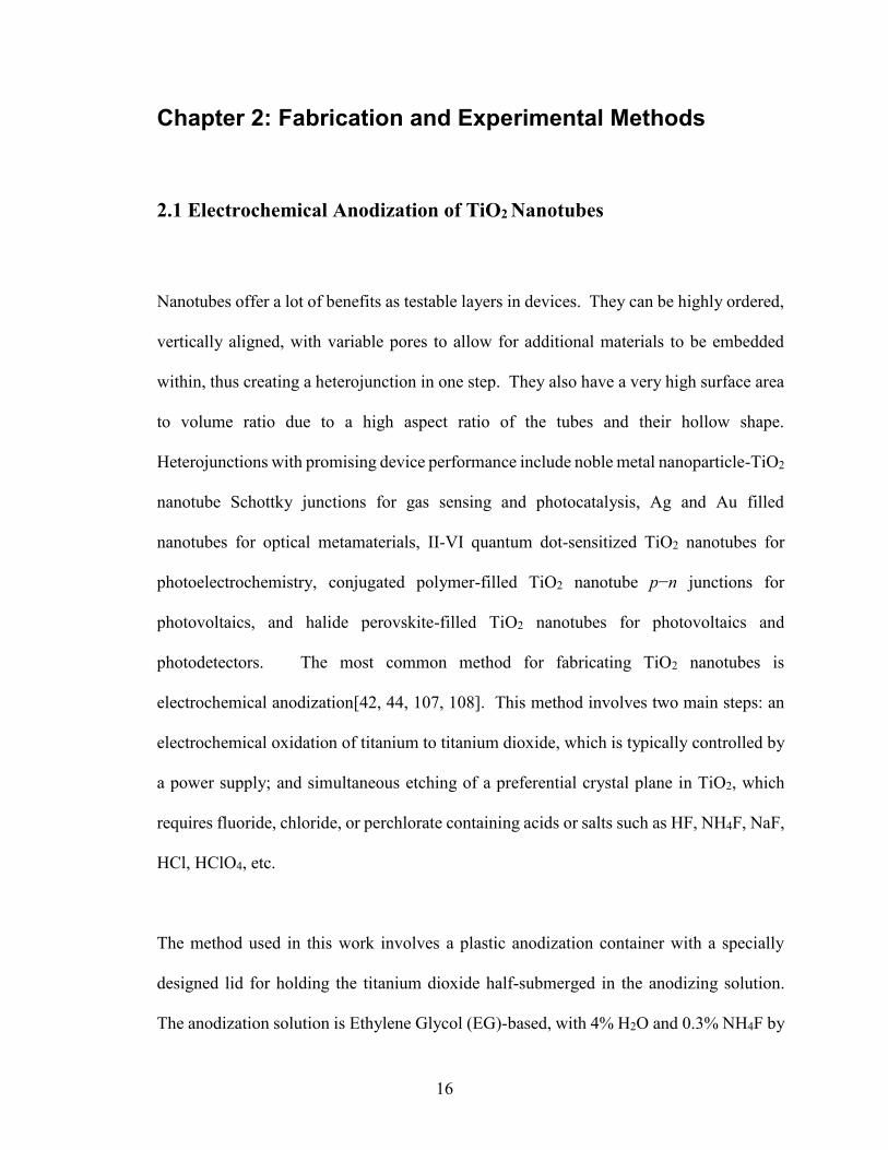
dioxide into nanotube shapes based on the chemical reactions in Figure 3. To control the
electric field, parafilm is used around the edges and back of the titanium foil so that the foil
closely mimics a parallel-plate capacitor by reducing fringing fields along the sides and
back of the samples. The temperature, water level, and distance between anode and
cathode is kept consistent between all experiments. The anode and cathode are cut at
specific dimensions of 1.5’’ by 0.5’’ and then cleaned with acetone, water, and methanol
in an ultrasonic bath for 10 minutes each.
Figure 3: The anodization reactions that govern TiO2 nanotube growth.
18
With the proper setup and reaction conditions, the process begins with a constant voltage
and initially a high current because the bare titanium foil is so easily oxidized to TiO2. As
the TiO2 layer thickens with time, current decreases quickly due to increased resistance
from the growing oxide layer. The current will then begin to plateau as the barrier layer
growth slows, and then will begin to reach an equilibrium barrier layer thickness as the
TiO2 is etched away, leaving pores that aid the flow of ions toward the titanium sheet
underneath. The pores continue to grow deeper into the TiO2 layer because that is where
the electric field is highest, and the path for ions and electrons faces the least resistance.
The end result is vertically oriented, highly uniform TiO2 nanotubes completely covering
the original titanium substrate. There is also a barrier layer, usually about 50-200 nm thick
separating the foil from the nanotubes. The nanotube walls will also be less thick at the
top compared to the base; this is because the top of the nanotubes forms first, and is slightly
etched over time due to the fluoride-based solution. Depending on the anodization
parameters, these nanotubes might be loosely attached to the original substrate, in which
case they can be delaminated without extensive damage to the structure[109]. This
delamination results in a nanotube layer that is fully detached from the substrate, and
depending on the thickness it can be very fragile, but also very useful for sensing
applications where the titanium substrate would hinder application.
The nanotubes grown this way are amorphous (and insulating), so an annealing step is
needed to bring them to a polycrystalline anatase phase (which is semiconducting). The
nanotubes are annealed at 450 ºC for 2 hours with a 10 sccm oxygen flow, to fill any
19
potential oxygen vacancies in the TiO2 crystals and to achieve better charge mobility
through the nanotubes. This process also mechanically strengthens the nanotube structure,
which can be especially important for the fragile nanotube membranes.
2.2 Solvothermal Growth of TiO2 Nanowires
TiO2 nanowires are similar to nanotubes in that they are organized, vertically oriented
nanostructures with flexible methods of growth allowing for variation in dimensions,
shapes, and crystal phase. Nanowires differ from nanotubes in that they are not hollow and
are monocrystalline as opposed to polycrystalline nanotubes. Nanowires also differ in that
they are fabricated using solvothermal methods, which involves performing a chemical
reaction under conditions of high temperature and pressure[110-112]. In practice, this
involves heating a specific solvent containing the required precursors under specific
temperature and pressure conditions in a teflon vessel to grow elemental or compound
nanowires on a desired substrate. Nanowire growth is simpler in that it only involves
heating a solvent above its critical point, and allowing the other agents in the solvent to
grow the nanowires in a bottom-up process. This growth only takes a few hours for
nanowires with a length of 1-5 microns. When the solvent is water, the growth process is
called hydrothermal synthesis. Hydrothermal growth leverages the changes in the
solubility of ions and ionic compounds in water as the critical point is approached, in order
to force precipitation of the desired compounds.
An additional benefit of the solvothermal growth technique is that it does not require any
high temperature annealing afterwards to form a crystalline or polycrystalline phase. The
20
process itself only requires heating to 180 ºC, and the TiO2 grows via a crystallization
process that results directly in rutile phase. This is useful because it matches the phase of
the conductive Fluorine-doped tin oxide (FTO) substrate and therefore strongly adheres to
that surface. The downside is that using other substrates is more difficult and requires a
seed layer of TiO2, added by spin or drop coating before the solvothermal treatment begins.
The solvothermal recipe typically involves three main precursors. First, a solvent that
dissolves the other precursors adequately at room temperature, but with a low enough
boiling point that it partially evaporates when heated allowing the precursors to precipitate
or crystallize out. Second, a TiO2 source, usually a large molecule that is weakly soluble
in the solvent; with heating, the loss of the solvent to evaporation will cause the TiO2 to
crystallize along every surface covered by the solution. Fortunately this process is
preferential to crystallization on the FTO substrate because of the matching crystal phases
and proximal lattice parameters (rutile: a = 0.4594, c = 0.2958, and FTO: a = 0.4737, c =
0.3185 nm)[113]. Third, a capping agent or stabilizing agent is required to grow nanotubes
of specific dimensions and spacings. The capping agent inhibits growth in certain crystal
phases or orientations, resulting in the 1D growth we see for nanowires. Since the process
is essentially due to random nucleation of the nanowires on the FTO surface, it is difficult
to control once started; however, we can selectively etch the FTO beforehand on a macro-
, micro-, or nano- scale. This pre-etching only allows nanowires to grow on the un-etched
sections of FTO, allowing us to engineer patterns or designs of nanowires on the substrate.
Our solvothermal recipe uses water as the solvent, making it a hydrothermal process. The
titanium precursor is titanium butoxide, a large and highly reactive organic molecule which
21
acts as a titanium and oxygen source in the reaction; it is shown in Figure 4. HCl is also
used as an additive to fix the pH to a low values, this ensures that the titanium precursor
dissolves readily but does not lyse, react, or decompose before the growth begins. The HCl
is also used for aligning the nanowires, inhibiting growth along the sidewalls of the TiO2
due to the selective adsorption of Cl− ions on the [110] family of surfaces, thus allowing
growth only in the [001] direction. An additional precursor, acetic acid is also used for
controlling the growth: acetic acid is a capping agent that enables control of the nanowire
size through its adsorption on to TiO2 surfaces, and also prevents the titanium dioxide from
crystallizing on the sidewalls of the Teflon container, which results in a more dense growth
of nanowires on the desired substrate.
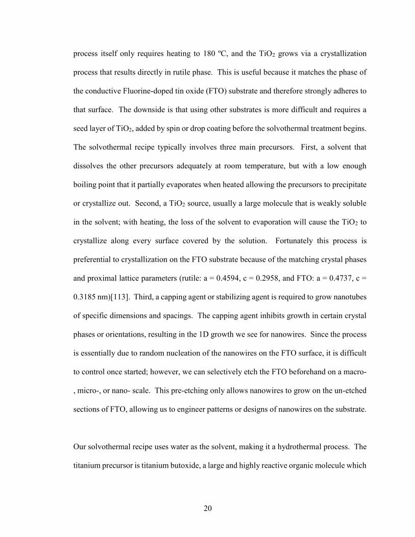
Figure 4: The chemical structure of titanium butoxide
The growth recipe consists of 100 μL of titanium butoxide (99% Sigma Aldrich) dissolved
in 5 mL deionized H2O, 2.5 mL acetic acid (99% Fisher Scientific), and 2.5 mL HCl (99%
Fisher Scientific). This is put in a teflon reaction vessel and a PARR reaction bomb heated
in an oven to 180 ºC. The cleaned FTO substrate is placed at an angle against the wall,
22
conductive side down. The growth begins when the solution begins to heat above its boiling
point, the amount of liquid solvent decreases, and the titanium precursor will hydrolyze at
the FTO surface, leaving TiO2 nucleation sites behind. Because these nucleation sites have
the rutile phase, further growth is preferential at these locations. Combined with the acetic
acid and HCl which control the growth orientation, nanowires will continue to grow until
they are removed from the solution or the temperature is lowered. This growth occurs over
4 hours and afterwards the solution is cooled under flowing water, the nanowire substrates
are removed and cleaned with methanol and dried under nitrogen. Longer growth is
possible but the glass substrate begins to lose its transparency if left too long in the growth
solution due to the extreme conditions.
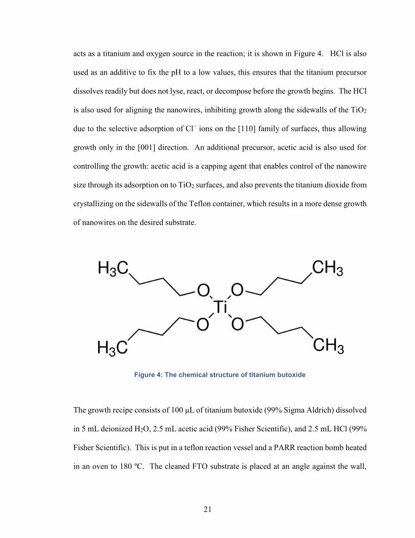
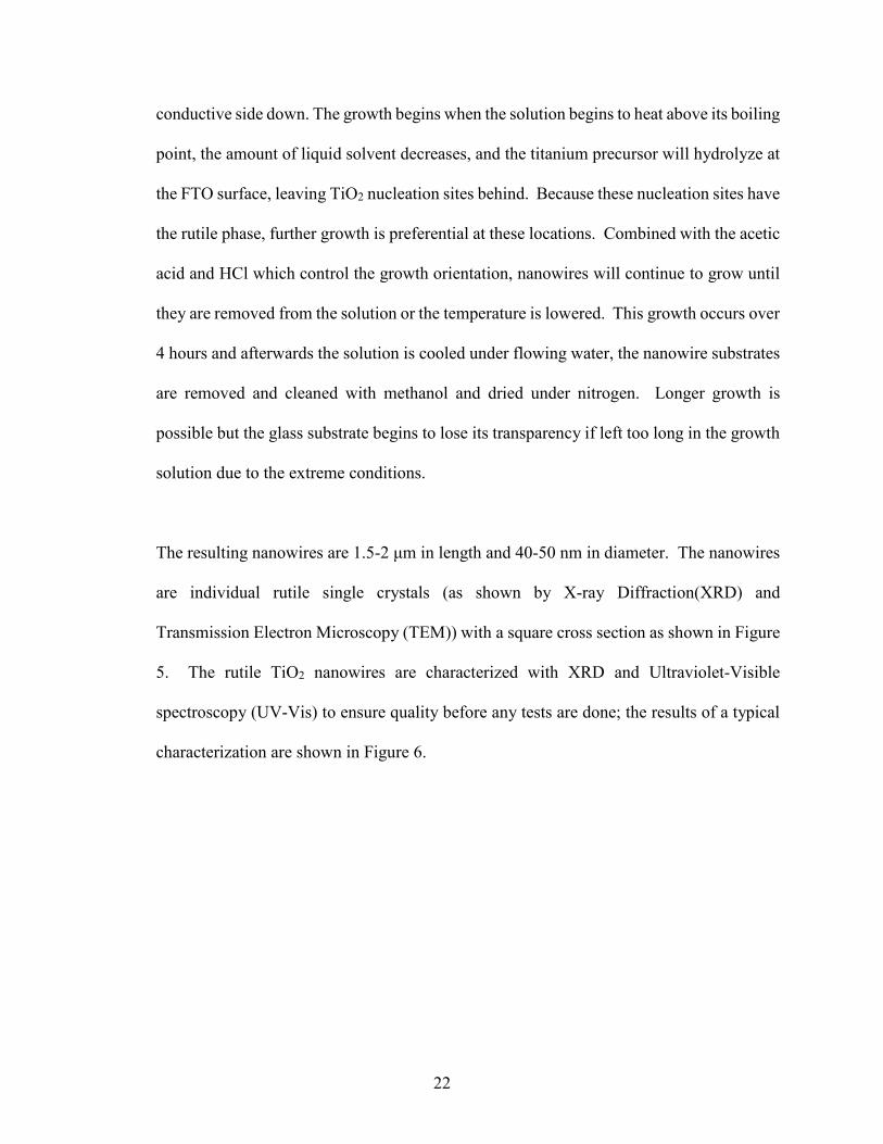
The resulting nanowires are 1.5-2 μm in length and 40-50 nm in diameter. The nanowires
are individual rutile single crystals (as shown by X-ray Diffraction(XRD) and
Transmission Electron Microscopy (TEM)) with a square cross section as shown in Figure
5. The rutile TiO2 nanowires are characterized with XRD and Ultraviolet-Visible
spectroscopy (UV-Vis) to ensure quality before any tests are done; the results of a typical
characterization are shown in Figure 6.
23
Figure 5: Rutile single crystal nanowires
Figure 6: XRD (A), UV-Vis (B), and TEM (C) of single crystal rutile nanowires
24
2.3 Formation of Self Assembled Monolayers
The addition of SAMs is often done to change the surface energy of a material. This work
was originally done on tuning the wettability of surfaces; where different perfluorinated
compounds were used to lower the surface energy of titanium nanotube arrays, resulting in
amphiphobic surfaces that are repellent to both water and organic solvents[79]. The
methods used are adapted from that work.
The SAMs were grown on TiO2 nanowire substrates. First a cleaning process is done using
oxygen plasma in a benchtop RIE Trion system. This clears the nanowires of debris such
as hydrocarbons or surface impurities from the anodization process. The oxygen plasma
also creates reactive oxygen on the surface of the TiO2 nanowires, increasing the adsorption
rate of the SAM. The oxygen plasma is formed using 50 mTorr oxygen under 250W RF
power, this is applied for 10 minutes to the sample and quickly followed by application of
the SAM.
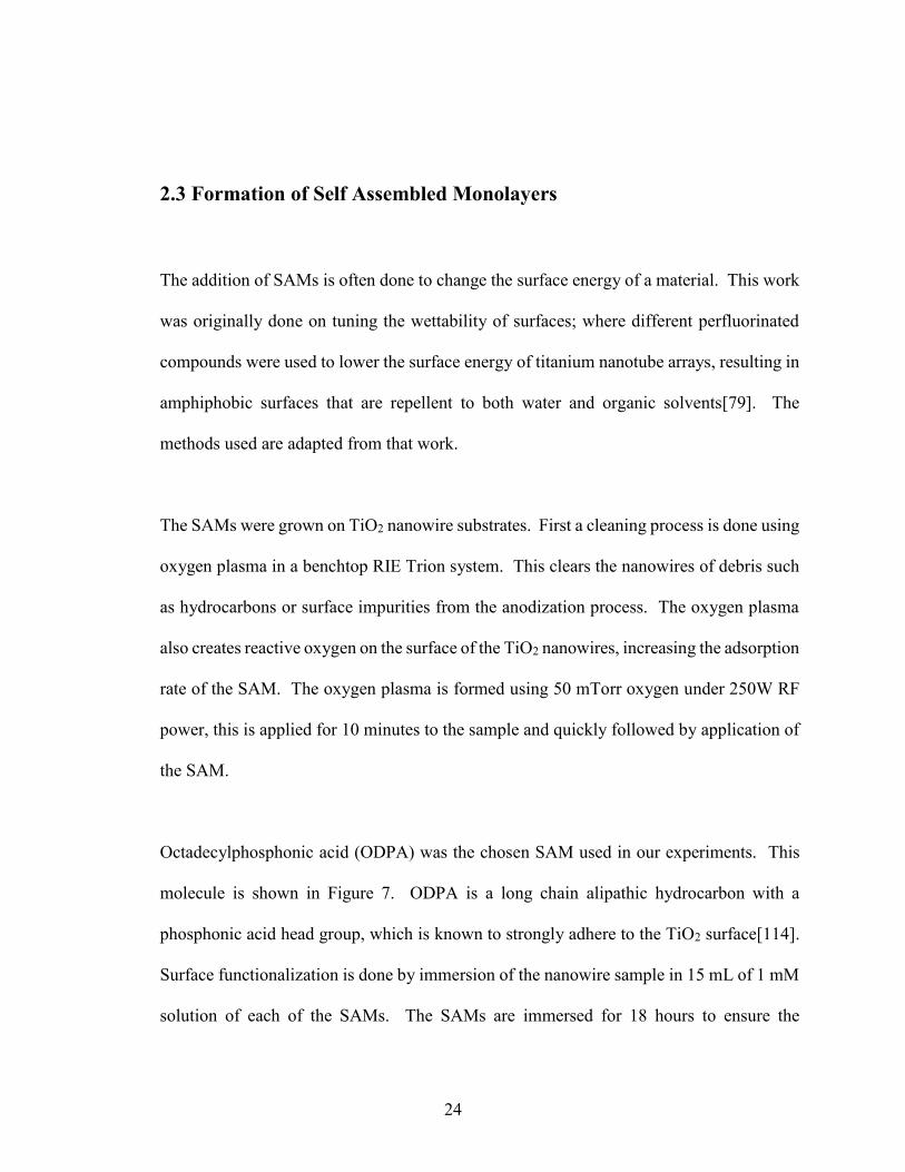
Octadecylphosphonic acid (ODPA) was the chosen SAM used in our experiments. This
molecule is shown in Figure 7. ODPA is a long chain alipathic hydrocarbon with a
phosphonic acid head group, which is known to strongly adhere to the TiO2 surface[114].
Surface functionalization is done by immersion of the nanowire sample in 15 mL of 1 mM
solution of each of the SAMs. The SAMs are immersed for 18 hours to ensure the
25
monolayer is highly packed and has a low defect density, this is done at room temperature
and in a sealed container. Methanol is used as the solvent because it will dissolve the
amphipolar SAM molecules while still allowing them to adsorb on the surface and self-
organize with few defects. Multiple studies have shown solvent choice to be important
when dealing with SAM formation, and that alcohol based solvents are most often
preferred[77]; we also found that water or other strongly polar solvents would disconnect
the TiO2 nanostructures from the FTO substrate.
Figure 7: The ODPA molecule chosen as a passivating SAM
After the 18 h of SAM formation, the substrates would be rinsed with methanol for 5
minutes to remove any excess SAM molecules that were not adsorbed directly on the
surface, then the substrates were dried under nitrogen. The substrates were tested with
UV-Visible spectroscopy but due to the thinness of the monolayer and the low absorption
of the organics it was identical to the bare nanowire substrate. Scanning Electron
Microscopy (SEM) also showed no signs of a monolayer because the thickness is only
expected to be ~ 1 nm, below the resolution limit of the machine. Fourier Transform
Infrared Spectroscopy (FTIR) was done using the Diffuse Reflection Infrared Fourier
Transform spectroscopy (DRIFTS) technique, which involves scratching off the nanowires
into a powder and measuring their infrared reflection against a background of KBr powder.
26
This method destroys the sample but it allows us to collect spectra from many identical
samples and acquire a lot of SAM-treated nanowire powder to find evidence of
functionalization. DRIFTS also uses an integrating sphere to collect all the scattered
infrared photons from the sample.
2.4 Carrier Dynamics: Characterization Methods
2.4.1 Time of Flight measurements
Time of flight is an optoelectronic characterization method that uses supra-bandgap light
to excite charge carriers into the conduction band where they will be free to move. These
carriers are created on one side of the material as a sheet of charge via a pulsed laser, and
an oscilloscope connected to the other side of the material will collect them and record the
transient signal.
In this time of flight experiment, a 337 nm nitrogen laser with a pulse rate of 20 Hz and a
pulse duration of 4 ns was used. Photons of this wavelength are strongly absorbed by the
TiO2 nanowire samples which is important to the Time of Flight (TOF) setup shown in
Figure 8.

27
Figure 8: The TOF setup used in our experiments, the oscilloscope measures at the gold
contacts. [115]
Light from the pulsed laser is illuminated on the sample from the FTO back side, it passes
through to the TiO2 nanostructures and is absorbed within the first 50-100 nm. At the top
of the nanostructures, on the front side of the sample, 200 nm of metal contact is deposited.
This metal is usually gold or aluminum which will form a uniform contact and collect the
charges. Gold is preferred due to its ability to consistently form a blocking contact which
is needed in order to ensure that excess carriers are not injected electrically from the top
contact while the sheet of charge is transiting through the nanowires. The layer is deposited
using e-beam evaporation, which is done at an angle to prevent gold from depositing to the
base of the nanostructures and causing a short. The thickness of this layer also helps when
connecting the contacts because it can protect the sample and prevent unwanted short
circuits due to pressure by the contact.
28
As the sample is illuminated by the light pulse and photogenerated charges move through
the material, a constant voltage is applied and they are collected from the metal contacts
and the transient photocurrent signal is read by an oscilloscope across a variable resistor.
TOF measurements can be performed either in small signal mode (wherein low level
injection conditions prevail) or in large signal mode (wherein high level injection is
present). The transient voltage vs. time information is recorded from this data and a typical
small signal TOF plot will look like Figure 9.
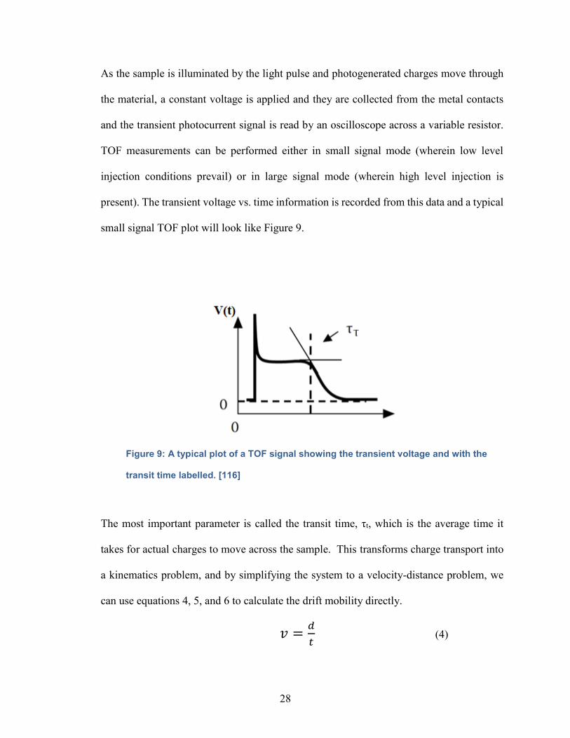
Figure 9: A typical plot of a TOF signal showing the transient voltage and with the
transit time labelled. [116]
The most important parameter is called the transit time, τt, which is the average time it
takes for actual charges to move across the sample. This transforms charge transport into
a kinematics problem, and by simplifying the system to a velocity-distance problem, we
can use equations 4, 5, and 6 to calculate the drift mobility directly.
𝑣 =𝑑
𝑡 (4)
29
Since velocity is determined by the mobility of the material and the applied field, we can
write this as;
𝜇𝐸 =𝑑
𝑡 (5)
Since our material is uniform from top to bottom, the field is constant, leading to;
𝜇 =𝑑2
𝑉𝑡 (6)
Thus by finding the transit time accurately, and knowing the applied voltage and the
distance (thickness of our nanostructures), the drift mobility can be directly measured for
many materials. This method is useful but there are many limitations on what can be
measured, and it is necessary to have good control over the length and doping of the
nanostructures.
The limitations arise because there are other transient signals in the system and their effect
must be kept separate from the transiting charge carriers[117]. The lower limit is due to
the inherent capacitance and resistance in the system. A resistor across the oscilloscope is
necessary to read the current as a voltage, there is also contact resistance at the metal-
nanowire junction. Also, because the sample is often quite densely populated by traps
which can store charges, there is a non-zero capacitance as well. The inherent capacitance
of the material and any depletion capacitance due to the blocking contact are other non-
negligible capacitances in the system. That means the circuit will act like an R-C circuit
when a signal is applied: the charges will collect in the sample, filling some of the traps
and reaching a dynamic equilibrium, but due to the non-zero resistance this will not happen
30
instantaneously so there is an RC time constant, τ = RC. It is important that this process
occurs much faster than the transit time, so that while charges are transiting the material
has already had time to reach steady state. The aforementioned capacitances are typically
in series due to which the smallest capacitance dominates the system response. It is also
necessary that the laser pulse duration is shorter than the transit time, to ensure the charges
are closely packed and similar to an ideal sheet of charge as they move through the material,
and an accurate transit time can be measured.
Time of flight measurements also have an upper limit, the transit time cannot be so slow
that the excited charge pulse disperses too much or that dielectric relaxation in the
semiconductor eliminates the electric field perturbation due to the injected pulse of
photogenerated charge carriers. A dispersed signal would be broad, and the transit time
(characterized by a sharp peak in the voltage) would not be visible. This broadening effect
is due to diffusion of the charge carriers. The time it takes for the electric field perturbation
to be eliminated is characterized by a dielectric relaxation time, τd. The dielectric
relaxation is a well-known effect in all electronics, and is defined by the expression;
τ𝑑 = 𝜀
𝜎 (7)
Where ε is the real permittivity of the material and σ is the conductivity.
Fortunately, because the materials dealt with are conjugated organic molecules or wide
bandgap semiconductors, their conductivity is often quite low, and the transit time is
comfortably smaller than the dielectric relaxation time. Due to the relatively low carrier
31
mobilities in these materials, any charge dispersion that occurs due to diffusion is not fast
enough to have an effect on the results.
2.4.2 Conductance, Capacitance, and Voltage measurements
Before measuring time of flight, the Current-Voltage (IV) curves, the Photocurrent-
Voltage curves a.k.a photoconductivity (PC) and Capacitance-Voltage (CV) curves are
measured for our material. This is done with a Keithley 4200-SCS Semiconductor
Parameter Analyzer. These tests show if the sample fabrication was successful, or if there
are short or open circuits due to deposition or growth problems. The IV curve will show
whether our material is conducting in the Ohmic, trap-filling, or space-charge limited
current (SCLC) regime. In the Ohmic regime, current follows the well-known trend of
equation 2. In the space-charge limited current regime, current becomes proportional to
voltage squared shown in the equation below[76];
𝐽 =9𝜀𝜀0𝜇𝑉2
8𝑑3 (8)
This equation arises in the SCLC regime because the field is no longer constant in the
material because of the non-negligible presence of excess charge carriers (assumed to be
unipolar). It is useful to identify an SCLC response in the material, and the voltage that
induces it because it can help characterize the types of traps and their density in the
material. It is also needed to help with time of flight calculations whenever the voltage
applied brings the material to exhibit an SCLC response. When an SCLC regime is clearly
32
evident in the IV characteristic, the drift mobility may be directly estimated using Eqn (9)
and can be used to verify the estimate from TOF measurements.
The PC measurement method can be used to find the mobility-lifetime product, μτ, of the
material, which is a key parameter related to how long excited charges exist in an excited
state, and how much current they conduct during their lifetime. This is done by measuring
the IV of a material under dark conditions, then again while the sample is under continuous
UV illumination to excite charge carriers. The difference in conductivity recorded is due
to an increase of charge carriers in the latter situation. A large change in conductivity can
be due to either a large mobility of the excess carriers, or a long lifetime (and subsequently
lots of excess carriers existing). This can be derived quickly by allowing the system to
reach steady-state, where the charge generation rate equals the charge recombination rate;
Rate of photons absorbed = ηIA
hυ =
𝑛−𝑛0
𝜏 = Rate of charge carriers recombined (9)
Where I is the intensity of the incident laser and A is the area of illumination, ν is the
frequency of the incident photons, and τ is the recombination time of charge carriers in
the material.
The excess charge carriers (n-no) are proportional to the change in conductivity based on
equation 2, giving us;
ηIA
hυ =
𝜎−𝜎0
𝑞𝜇𝜏 (10)
33
Leading to;
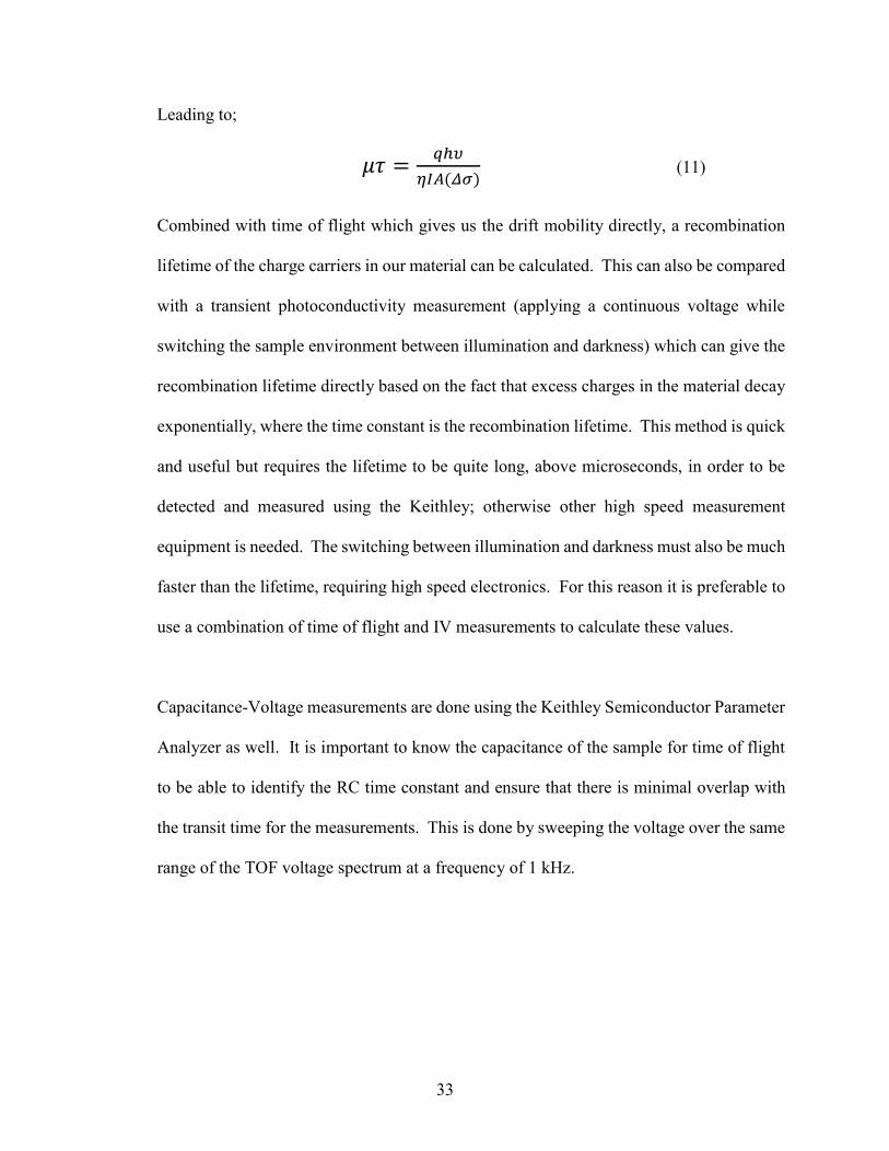
𝜇𝜏 =𝑞ℎ𝜐
𝜂𝐼𝐴(𝛥𝜎) (11)
Combined with time of flight which gives us the drift mobility directly, a recombination
lifetime of the charge carriers in our material can be calculated. This can also be compared
with a transient photoconductivity measurement (applying a continuous voltage while
switching the sample environment between illumination and darkness) which can give the
recombination lifetime directly based on the fact that excess charges in the material decay
exponentially, where the time constant is the recombination lifetime. This method is quick
and useful but requires the lifetime to be quite long, above microseconds, in order to be
detected and measured using the Keithley; otherwise other high speed measurement
equipment is needed. The switching between illumination and darkness must also be much
faster than the lifetime, requiring high speed electronics. For this reason it is preferable to
use a combination of time of flight and IV measurements to calculate these values.
Capacitance-Voltage measurements are done using the Keithley Semiconductor Parameter
Analyzer as well. It is important to know the capacitance of the sample for time of flight
to be able to identify the RC time constant and ensure that there is minimal overlap with
the transit time for the measurements. This is done by sweeping the voltage over the same
range of the TOF voltage spectrum at a frequency of 1 kHz.
34
2.5 Photoluminescence, Quantum Yield, and Time Resolved
Photoluminescence
2.5.1 Fabrication of Photoluminescent Tellurophenes
Phosphorescent tellurophenes were made by the Rivard group at the University of Alberta.
This was done for a study on their photoluminescent properties and later their conductive
properties as a thin film, and the results will be discussed later in chapter X.
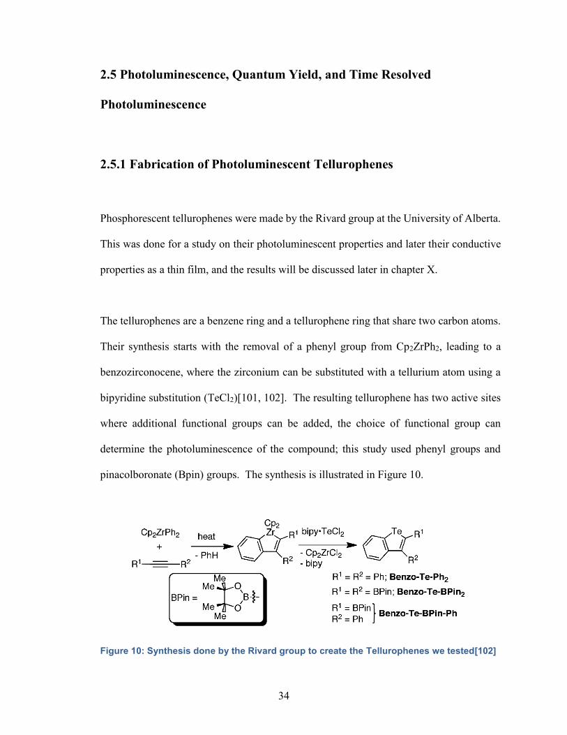
The tellurophenes are a benzene ring and a tellurophene ring that share two carbon atoms.
Their synthesis starts with the removal of a phenyl group from Cp2ZrPh2, leading to a
benzozirconocene, where the zirconium can be substituted with a tellurium atom using a
bipyridine substitution (TeCl2)[101, 102]. The resulting tellurophene has two active sites
where additional functional groups can be added, the choice of functional group can
determine the photoluminescence of the compound; this study used phenyl groups and
pinacolboronate (Bpin) groups. The synthesis is illustrated in Figure 10.
Figure 10: Synthesis done by the Rivard group to create the Tellurophenes we tested[102]
35
2.5.2 Measuring Photoluminescence and Recognizing Unwanted
Scattering
Photoluminescence of materials is commonly measured to gather information on their light
emission properties and underlying carrier dynamics. For most materials with a direct band
gap, this can give information on the band gap energy and for some materials, information
on any excitons generated in the material.
Photoluminescence measurements are done by exciting a material with an excitation beam
or excitation wavelength. Monochromatic illumination from a continuous wave (CW) laser
is sometimes used. More commonly, a broad spectrum light source such as a Xe arc lamp
is coupled with a programmable monochromator with tunable slit widths to select the
excitation wavelength window of interest. At the same time, a detector is present near the
material and will collect an emission spectrum from the sample. The alternative can also
be measured, where a specific emission is collected; and a scan of excitation wavelengths
is recorded to see which produces the most desired emission. A Cary Eclipse
spectrofluorometer system measured and recorded the intensities of the emission and
excitation wavelengths. For these measurements, fibre optic cables were used as sources
and collectors for the excitation and emission wavelengths respectively, they were
connected with a special module allowing their use. The fibre optic cables allow freedom
to adjust the incident and collecting angle of the light, helping to avoid unwanted specular
reflection being incorrectly measured by the machine as emission from the sample.
36
Common physical phenomena that can make the results of photoluminescence
measurements inaccurate are Raman scattering and particularly strong Mie scattering, and
is so often seen in these measurements that it should be explained. A simple method for
recognizing scattering and reducing the effect of unwanted scattering will also be
described. Scattering, unlike photoluminescence, does not require a photon with specific
energy to excite an electron to a higher energy state. Scattering, involves an electron in the
material being excited to a virtual energy state that is short lived, and not based on the real
band structure of the material[118]. As this electron decays, it normally decays to the same
energy level it was at originally, and this is just normal reflection. Sometimes; however,
the electron will decay to a higher state than it started, such as a higher energy vibrational
or rotational state. When this happens, the photon re-emitted by the decay process has a
different energy than the original photon (the scattering is therefore inelastic), exactly equal
to the difference between the original state and the higher vibrational/rotational state. This
can happen regardless of the excitation wavelength, but the difference in energy will
always be constant. Scattering peaks are often sharper than photoluminescence peaks
because they are based on the width of the excitation source, which is quite sharp. In order
to avoid confusing scattering as photoluminescence, multiple scans should be done with
slightly offset excitation wavelengths of 10-15 nm. Any scattering peaks will be offset by
approximately the same amount depending on the excitation, whereas real
photoluminescence peaks will be at a consistent location, because they are based on
electronic decays between real electronic states, as long as the excitation wavelength is
sufficiently absorbed.
37
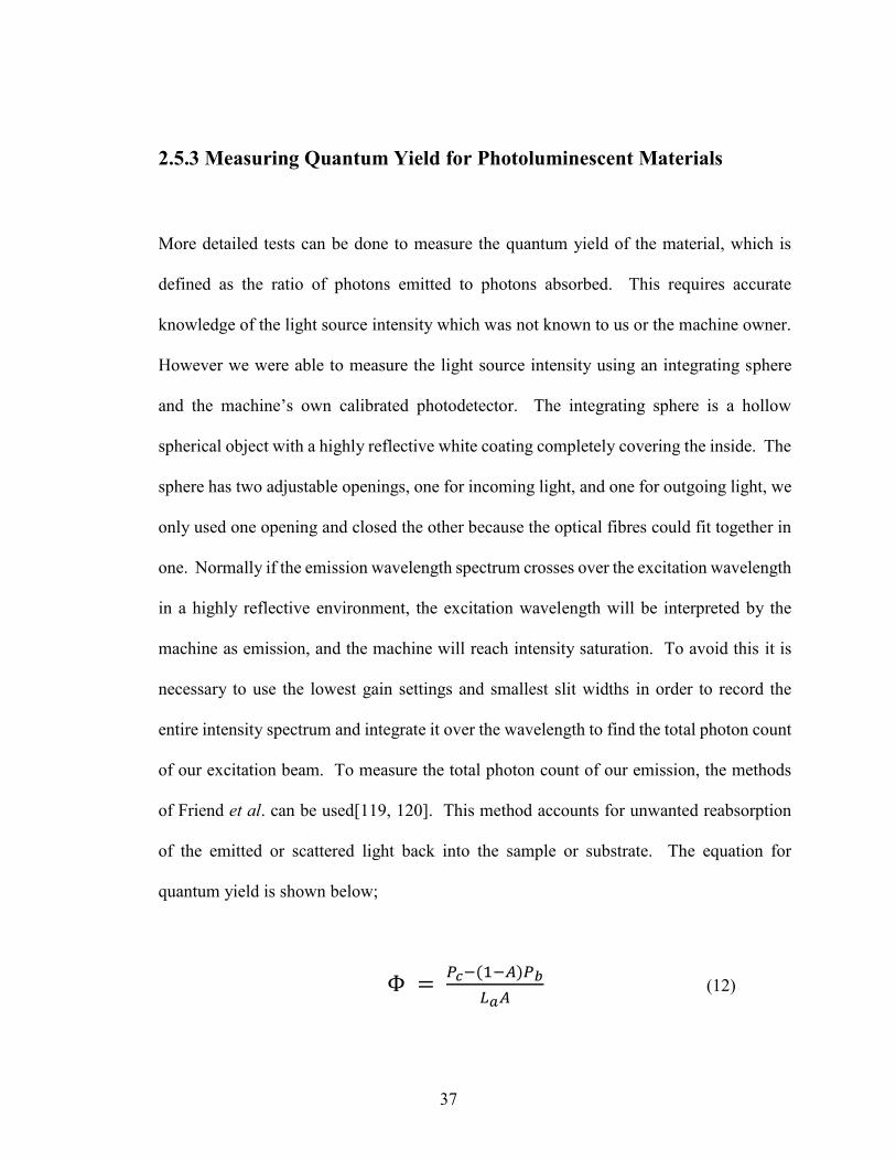
2.5.3 Measuring Quantum Yield for Photoluminescent Materials
More detailed tests can be done to measure the quantum yield of the material, which is
defined as the ratio of photons emitted to photons absorbed. This requires accurate
knowledge of the light source intensity which was not known to us or the machine owner.
However we were able to measure the light source intensity using an integrating sphere
and the machine’s own calibrated photodetector. The integrating sphere is a hollow
spherical object with a highly reflective white coating completely covering the inside. The
sphere has two adjustable openings, one for incoming light, and one for outgoing light, we
only used one opening and closed the other because the optical fibres could fit together in
one. Normally if the emission wavelength spectrum crosses over the excitation wavelength
in a highly reflective environment, the excitation wavelength will be interpreted by the
machine as emission, and the machine will reach intensity saturation. To avoid this it is
necessary to use the lowest gain settings and smallest slit widths in order to record the
entire intensity spectrum and integrate it over the wavelength to find the total photon count
of our excitation beam. To measure the total photon count of our emission, the methods
of Friend et al. can be used[119, 120]. This method accounts for unwanted reabsorption
of the emitted or scattered light back into the sample or substrate. The equation for
quantum yield is shown below;
Φ = 𝑃𝑐−(1−𝐴)𝑃𝑏
𝐿𝑎𝐴 (12)
38
Where A is the fraction of light absorbed by the sample from the initial beam, La is the
photon count of the emission beam, Pc is the emitted photon count when the beam is aligned
to hit the sample in the integrating sphere, and Pb is the emitted photon count when the
beam is not aligned with the sample, but the sample is still in the integrating sphere. The
quantum yield is an important parameter because it is a huge factor in determining whether
the material can be used efficiently in LEDs or OLEDs, or as a photoluminescent marker
material.
2.5.4 Measuring Time-Resolved Photoluminescence
Measuring time-resolved photoluminescence utilizes the same principles as regular
photoluminescence tests. A light source is used to excite electrons in the material, and
these need to be captured and recorded along with the elapsed time. A pulsed light source
is required and it is synchronized with the oscilloscope so that every laser pulse sets the
time to 0. A 337 nm laser source is used because the photoluminescence is previously
known to be strong at that excitation. A large diameter lens system placed close to the
sample collects emitted photoluminescence from a relatively large solid angle and
magnifies any and all light coming from the material towards a monochromator, which
blocks all wavelengths that do not match the known photoluminescence peak. With this
system properly implemented, the only light that passes through the monochromator should
be photoluminescence from the sample. The monochromator is directly connected to a
detector and to prevent unwanted loss of the emitted light and reduce signal noise from the
environment.
39
To measure the fast lifetimes of photoluminescence, it is necessary to be able to track
changes over the nanosecond time range. A photomultiplier tube was able to sample the
intensity every 10 nanoseconds so it would be able to capture phosphorescent emission and
any fluorescent emission would be noticeable. At these high speeds a very high gain is
required because there is very little light to be detected during that short time, but care
should be taken so that light from the environment cannot enter the detector system or it
can overload and break the device. The photomultiplier tube can transfer measurements to
the oscilloscope which has already been synced with the laser pulse. This way the data
recorded is easily read and analyzed.
To analyze the recombination lifetime of the material, the data is fit to an exponential curve;
with no limit on the number of terms if it seems like there are multiple pathways to emission
(bi-exponential, tri-exponential, etc.) The samples may also have fluorescent and
phosphorescent components, so it is important to record data over large and small time
intervals.
2.6 Microwave Resonators and Microwave Characterization
The ring-type microwave resonators used in this section were designed by the Daneshmand
group in the ECE Department at the University of Alberta. The design and simulation
work done on them had been completed beforehand by Zarifi et al[121]. This section is
40
designed to introduce their use in characterizing semiconductor material properties, also
known as time resolved microwave conductivity (TRMC) measurements.
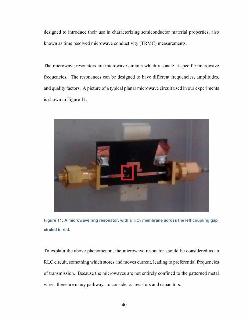
The microwave resonators are microwave circuits which resonate at specific microwave
frequencies. The resonances can be designed to have different frequencies, amplitudes,
and quality factors. A picture of a typical planar microwave circuit used in our experiments
is shown in Figure 11.
Figure 11: A microwave ring resonator, with a TiO2 membrane across the left coupling gap
circled in red.
To explain the above phenomenon, the microwave resonator should be considered as an
RLC circuit, something which stores and moves current, leading to preferential frequencies
of transmission. Because the microwaves are not entirely confined to the patterned metal
wires, there are many pathways to consider as resistors and capacitors.
41
Fortunately, the ring length and width are the most important factors in determining the
resonance properties of the circuit, and will determine the resonance frequency. However,
the coupling gap can also act as a capacitor and store charge. Because the coupling gap
closely mimics a parallel plate capacitor, it is well-studied and understood. Small changes
in the coupling gap environment, especially when the resonator has a high quality factor,
can result in measurable changes in the resonance frequency profile, and those changes can
be interpreted to provide information on the material present in the gap. For example, a
material with a high dielectric constant, ε, placed within the gap will cause the capacitance
of the gap to increase based on the dielectric equation;
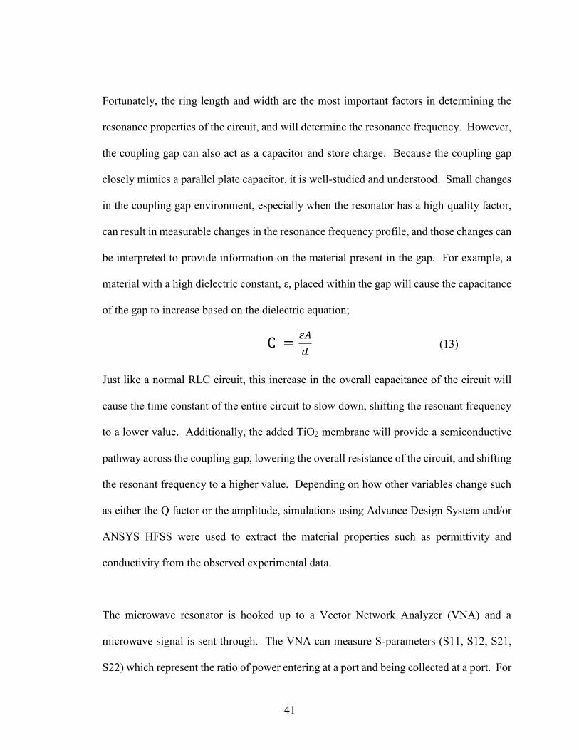
C =𝜀𝐴
𝑑 (13)
Just like a normal RLC circuit, this increase in the overall capacitance of the circuit will
cause the time constant of the entire circuit to slow down, shifting the resonant frequency
to a lower value. Additionally, the added TiO2 membrane will provide a semiconductive
pathway across the coupling gap, lowering the overall resistance of the circuit, and shifting
the resonant frequency to a higher value. Depending on how other variables change such
as either the Q factor or the amplitude, simulations using Advance Design System and/or
ANSYS HFSS were used to extract the material properties such as permittivity and
conductivity from the observed experimental data.
The microwave resonator is hooked up to a Vector Network Analyzer (VNA) and a
microwave signal is sent through. The VNA can measure S-parameters (S11, S12, S21,
S22) which represent the ratio of power entering at a port and being collected at a port. For
42
example, S21 represents the ratio of power entering from port 1 that is collected at port 2
(transmission), whereas S11 measures power entering at port 1 and being collected at port
1 (reflection). S parameters are typically measured in decibels (dB). The vector network
analyzer can gives us a frequency spectrum of the chosen S parameter and a visual user
interface allows us to quickly find the resonant peak we want to study.
The idea of TRMC measurements using this system comes from the fact that the VNA is
able to measure an entire spectrum in about 10 milliseconds. Thus any long lived, time-
dependent material changes can be detected using the microwave resonator circuit without
moving or disturbing the environment. UV light excitation of TiO2 nanotube membranes
was used as the test material. The UV light excites charge carriers, which leads to a change
in the complex permittivity of the membrane, and the long carrier lifetime in the TiO2
nanostructures (mostly due to carrier trapping) causes a very slow return to equilibrium
when the light is turned off. This entire cycle can be measured using the VNA, and the
material parameters constantly calculated at each time interval. Similar to the TRPL
measurement, the recombination lifetime of carriers can be measured by fitting the data to
a multi-exponential decay curve. This means we can calculate recombination of carriers
without requiring radiative recombination or emission from the sample.
The use of planar ring resonators is an upgrade over the previous technology, resonant
cavity waveguides. These were larger and bulkier and harder to use than the planar
resonators developed by the Daneshmand group. Tuning and making planar resonators is
also easier than replacing the large parts of a cavity waveguide. The planar resonators are

43
also more conducive to measurements of a substrate’s changing environment, whereas the
cavity waveguide environment is fixed and previous research has not focused on
manipulating it for purposes like gas, liquid, or humidity sensing.
44
Chapter 3: Experimental Results and Analysis
3.1 Charge Carrier Dynamics of Functionalized TiO2 Nanowires
3.1.1 Experimental Setup
One of the key goals of this research project is to improve the understanding of our TiO2
nanowires, and if possible, use them in devices such as solar cells, gas sensors, LEDs, or
transistors. Previous experiments calculating the mobility of TiO2 have been successful on
the bulk material (large single crystals of rutile), but transport within nanostructures had
been much less studied, and TOF had not been done. Other measurement techniques such
as Hall Mobility did not work with our nanostructures because of the conductive FTO
below, which acts as a secondary pathway for lateral transport. To characterize the
nanowires it was necessary to measure the charge transport along the nanowire axis. Based
on the initial results, we then tried to improve the nanowires’ charge transport properties
using SAM functionalization.
The experiment started by making multiple TiO2 nanowire arrays using the process
described in chapter 2. Fluorine doped tin oxide (FTO) was cleaned by immersion in
acetone, methanol, and then water under ultrasonication. The FTO was dried with nitrogen
and individually put in a solution of 5 mL H2O, 2.5 mL HCl, 2.5 mL Acetic acid, and 200
μL titanium butoxide in a PARR reaction vessel, with the conductive FTO side facing
diagonally downwards. The reaction vessel loaded with FTO was kept at 180ºC for 4
hours, then cooled in flowing water for 30 minutes and the FTO- rutile nanowire substrate
was rinsed with methanol and dried under nitrogen. The nanowire array substrate was then
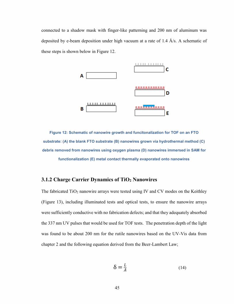
45
connected to a shadow mask with finger-like patterning and 200 nm of aluminum was
deposited by e-beam deposition under high vacuum at a rate of 1.4 Å/s. A schematic of
these steps is shown below in Figure 12.
Figure 12: Schematic of nanowire growth and funcitonalization for TOF on an FTO
substrate: (A) the blank FTO substrate (B) nanowires grown via hydrothermal method (C)
debris removed from nanowires using oxygen plasma (D) nanowires immersed in SAM for
functionalization (E) metal contact thermally evaporated onto nanowires
3.1.2 Charge Carrier Dynamics of TiO2 Nanowires
The fabricated TiO2 nanowire arrays were tested using IV and CV modes on the Keithley
(Figure 13), including illuminated tests and optical tests, to ensure the nanowire arrays
were sufficiently conductive with no fabrication defects; and that they adequately absorbed
the 337 nm UV pulses that would be used for TOF tests. The penetration depth of the light
was found to be about 200 nm for the rutile nanowires based on the UV-Vis data from
chapter 2 and the following equation derived from the Beer-Lambert Law;
δ = 𝐿𝐴 (14)
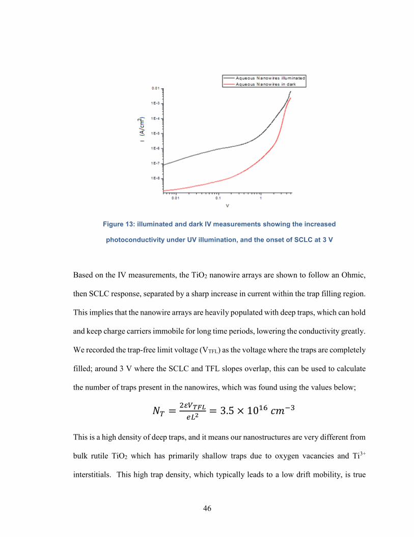
46
Figure 13: illuminated and dark IV measurements showing the increased
photoconductivity under UV illumination, and the onset of SCLC at 3 V
Based on the IV measurements, the TiO2 nanowire arrays are shown to follow an Ohmic,
then SCLC response, separated by a sharp increase in current within the trap filling region.
This implies that the nanowire arrays are heavily populated with deep traps, which can hold
and keep charge carriers immobile for long time periods, lowering the conductivity greatly.
We recorded the trap-free limit voltage (VTFL) as the voltage where the traps are completely
filled; around 3 V where the SCLC and TFL slopes overlap, this can be used to calculate
the number of traps present in the nanowires, which was found using the values below;
𝑁𝑇 =2𝜀𝑉𝑇𝐹𝐿
𝑒𝐿2 = 3.5 × 10¹⁶ 𝑐𝑚−3
This is a high density of deep traps, and it means our nanostructures are very different from
bulk rutile TiO2 which has primarily shallow traps due to oxygen vacancies and Ti3+
interstitials. This high trap density, which typically leads to a low drift mobility, is true
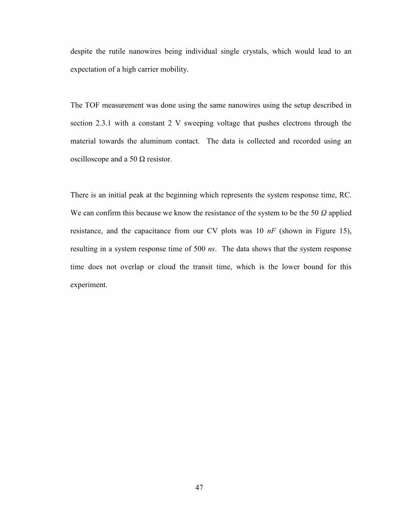
47
despite the rutile nanowires being individual single crystals, which would lead to an
expectation of a high carrier mobility.
The TOF measurement was done using the same nanowires using the setup described in
section 2.3.1 with a constant 2 V sweeping voltage that pushes electrons through the
material towards the aluminum contact. The data is collected and recorded using an
oscilloscope and a 50 Ω resistor.
There is an initial peak at the beginning which represents the system response time, RC.
We can confirm this because we know the resistance of the system to be the 50 Ω applied
resistance, and the capacitance from our CV plots was 10 nF (shown in Figure 15),
resulting in a system response time of 500 ns. The data shows that the system response
time does not overlap or cloud the transit time, which is the lower bound for this
experiment.
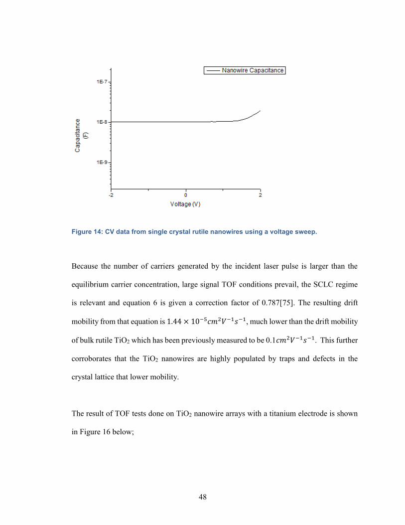
48
Figure 14: CV data from single crystal rutile nanowires using a voltage sweep.
Because the number of carriers generated by the incident laser pulse is larger than the
equilibrium carrier concentration, large signal TOF conditions prevail, the SCLC regime
is relevant and equation 6 is given a correction factor of 0.787[75]. The resulting drift
mobility from that equation is 1.44 × 10⁻⁵𝑐𝑚2𝑉−1𝑠−1, much lower than the drift mobility
of bulk rutile TiO2 which has been previously measured to be 0.1𝑐𝑚2𝑉−1𝑠−1. This further
corroborates that the TiO2 nanowires are highly populated by traps and defects in the
crystal lattice that lower mobility.
The result of TOF tests done on TiO2 nanowire arrays with a titanium electrode is shown
in Figure 16 below;
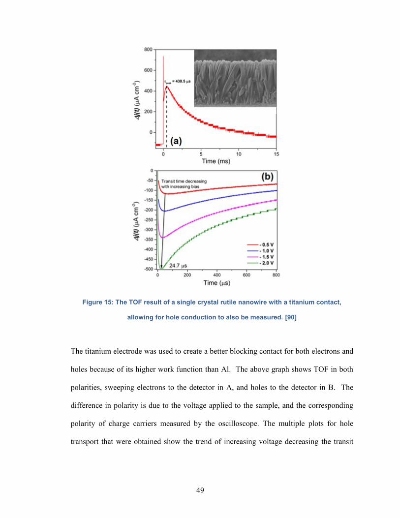
49
Figure 15: The TOF result of a single crystal rutile nanowire with a titanium contact,
allowing for hole conduction to also be measured. [90]
The titanium electrode was used to create a better blocking contact for both electrons and
holes because of its higher work function than Al. The above graph shows TOF in both
polarities, sweeping electrons to the detector in A, and holes to the detector in B. The
difference in polarity is due to the voltage applied to the sample, and the corresponding
polarity of charge carriers measured by the oscilloscope. The multiple plots for hole
transport that were obtained show the trend of increasing voltage decreasing the transit
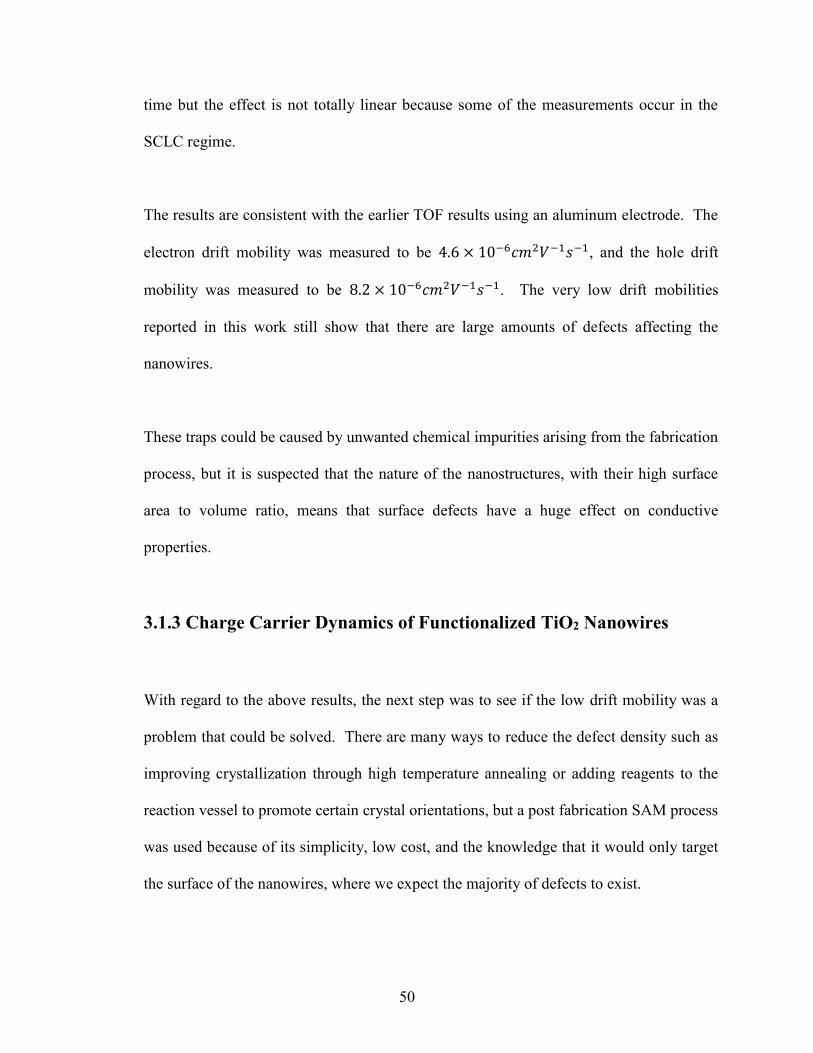
50
time but the effect is not totally linear because some of the measurements occur in the
SCLC regime.
The results are consistent with the earlier TOF results using an aluminum electrode. The
electron drift mobility was measured to be 4.6 × 10⁻⁶𝑐𝑚2𝑉−1𝑠−1, and the hole drift
mobility was measured to be 8.2 × 10⁻⁶𝑐𝑚2𝑉−1𝑠−1. The very low drift mobilities
reported in this work still show that there are large amounts of defects affecting the
nanowires.
These traps could be caused by unwanted chemical impurities arising from the fabrication
process, but it is suspected that the nature of the nanostructures, with their high surface
area to volume ratio, means that surface defects have a huge effect on conductive
properties.
3.1.3 Charge Carrier Dynamics of Functionalized TiO2 Nanowires
With regard to the above results, the next step was to see if the low drift mobility was a
problem that could be solved. There are many ways to reduce the defect density such as
improving crystallization through high temperature annealing or adding reagents to the
reaction vessel to promote certain crystal orientations, but a post fabrication SAM process
was used because of its simplicity, low cost, and the knowledge that it would only target
the surface of the nanowires, where we expect the majority of defects to exist.
51
Before the SAM is added, the nanowire array undergoes an oxygen plasma cleaning
process. Then an octadecylphosphonic acid (ODPA) SAM was added onto the nanowire
substrate by dissolving 1 mM of ODPA in a 4:1 solution of isopropanol to water, and
immersing the sample for 18 hours. This was done both pre- and post- deposition of the
metal contact in case the deposition process caused the organic ODPA to overheat and
break down; it was found that adding the ODPA before the metal deposition worked better
to improve the drift mobility of the nanowire arrays, because with post-deposition the
ODPA did not reach underneath the deposited metal to the nanowires that would be
carrying current. The ODPA should align itself along the surface of the nanowires, but it
is not expected to conduct itself because it is a long, unconjugated organic molecule. The
ODPA can bind in multiple ways based on how to oxygen molecules orient themselves to
the surface; this is known as the denticity of the molecule and is exhibited in Figure 16.
Figure 16: The different possible orientations (denticities) of ODPA on TiO2 [122]

52
Characterization of the SAM was performed primarily by FTIR analysis shown in Figure
17.
Figure 17: FTIR data using DRIFTS on ODPA-functionalized nanowire samples [90]
The FTIR data was collected in DRIFTS mode, and it shows the expected phosphonate
peaks at 1010 cm-1 and 1119 cm-1, which indicates that the ODPA is bonded to TiO2 [123].
Unbound phosphonate peaks occur at 1075 cm-1 and 950 cm-1 but they are not seen,
indicating the ODPA is completely bound to the nanowires, and no excess unbound ODPA
is present[124]. The additional CH3 symmetric and anti-symmetric peaks at 2850 cm-1 and
2950 cm-1 show the presence of the organic tail of the ODPA, and none of the peaks listed
above occurred in the bare nanowire DRIFTS reading.

53
The benefit of the titanium metal contact on the unpassivated nanowires in figure 15 was
that we could measure the transit of both electrons and holes using this configuration, since
Ti exhibited superior blocking action for electrons than Al, which ensured that
photogenerated holes were not completely lost to recombination with electrically injected
electrons. We found this blocking effect was even more pronounced using a platinum
electrode with a work function of 6.35 eV. For this reason, TOF tests using a platinum
electrode were performed in order to see both electron and hole transient photo-currents,
the results are shown in Figure 18 below.
Figure 18: The IV curve for ODPA-passivated nanowires with a platinum electrode. Black
represents a positive potential and green a negative potential at the Pt contact. Adapted
from [90]

54
The IV curve for the ODPA-functionalized nanowires (Figure 17) shows an SCLC
response, but does not have a trap-filling region where the current grows faster than V2.
Instead it has a smooth curve transitioning from the Ohmic regime (J α V) to the SCLC
regime (J α V2) This indicates that the traps are no longer high energy deep traps, but low
energy shallow traps. This is indicative of the passivation of the traps. Essentially, the
phosphonate head group chemisorbs to a dangling bond at the surface, eliminating the trap.
In addition, the close-packed hydrophobic alkyl chains block the entry of water molecules
and hydroxyl groups near the nanowire surface and thus prevent the capture of free
electrons and holes by chemisorbed water and hydroxyl ions respectively. Based on the
SCLC current-voltage relation (equation 8) being applied at the pink line where the SCLC
regime begins; the electron and hole mobility are found to be 2.7 × 10⁻⁴𝑐𝑚2𝑉−1𝑠−1 and
5.5 × 10⁻³𝑐𝑚2𝑉−1𝑠−1, respectively, already an increase of ~100x relative to the
unpassivated nanowires.
The TOF measurements done on the functionalized samples used the same procedure as
the non-functionalized nanowire tests, the only difference was the switch to a platinum
electrode for better blocking behavior. The results for the functionalized nanowire samples
are shown in Figure 19.

55
Figure 19: TOF data for electrons (a) and holes (b) for ODPA-functionalized nanowires.
Adapted from [90]
The graphs show the same features as earlier TOF tests; the trend of transit time decreasing
with voltage, and the sharp peak leading to a slower decay as the excess carriers trap and
recombine. The hole transport peak is sharper, which suggests that the trapping of holes
in ODPA-passivated rutile phase TiO2 is less severe than that of electrons. Too much
dissipation of the signal would result in the transit time being indistinguishable; and this is
related to equation 5: the upper bound of TOF measurements being equal to the dielectric
relaxation time. From the TOF plots in Figure 19, the electron mobility is found to be
4.3 × 10⁻⁴𝑐𝑚2𝑉−1𝑠−1 and the hole mobility higher: 7.1 × 10⁻³𝑐𝑚2𝑉−1𝑠−1, which is
almost 1000x higher than when unpassivated.
56
3.1.4 Discussion
The charge carrier dynamics tests done in this section are useful but not commonly used
measurements that can work with a wide variety of materials. The analysis of IV curves
into the SCLC regime is highly necessary for materials with low equilibrium carrier
concentrations, but for most commercial semiconductors like silicon and germanium, this
limit is not often reached. The IV analysis to find mobility closely matches the TOF
analysis in terms of result, with a maximum error of ~30% (TOF passivated electron
mobility 4.3 vs IV passivated electron mobility 2.7). But this can be considered minor
when dealing with huge improvements in order of magnitude. TOF is also especially useful
for measuring mobility as an alternative to systems that utilize the Hall Effect; especially
in devices that are multilayered, since the other layers may have undesired charge transport
and the material of interest would be difficult to isolate.
More importantly, both measurement methods were decisive in showing that passivation
of the nanowires using ODPA was possible and effective in reducing the number of deep
traps, increasing conduction, and improving mobility of both electrons and holes. The
results show that deep traps on the surface are a large factor in restricting the charge carrier
mobility in TiO2 nanowires. The extent that this can be improved by surface passivation
was shown to be at least 100-1000x but there is much more room for improvement to reach
the mobility of bulk TiO2. It is unclear if the surface passivation completely nullified the
effect of surface defects, or if it only passivated a portion of them. Either way, it is likely
the procedure could be adapted to other devices or materials, especially nanostructured
57
materials such as silicon nanowires and zinc oxide thin films where surface traps are most
likely to have a large effect.
The goal of continued research in this field is twofold; the first is simple: to apply
passivation layers to TiO2 nanostructures for use in solar cell devices, and the results in
this chapter are already being used for that purpose. The second: to find other SAM
materials that can act as passivation layers which may be better than the ODPA used here.
There are many organic molecules that are candidates for passivating SAMs, and many
nanostructured materials to use them on; further study could consist of simulating trap
passivation or developing a model that could narrow the search.
3.2 Characterization of TiO2 Nanostructures using Microwave
Resonators
Planar microwave resonators are useful devices developed by the Daneshmand group that
can give us information on a material’s complex dielectric constant, even as it changes over
time. We used these planar microwave resonators to measure the time-resolved microwave
conductivity of our TiO2 nanotube membranes, before and after functionalization.
58
3.2.1 Experimental setup
The membranes were prepared by growing TiO2 nanotubes on titanium foil substrates.
This meant cleaning the foil substrates by immersion in acetone, methanol, and then water
under ultrasonic application. The anodization solution was 4% DI water, 0.3% NH4F by
mass, dispersed in ethylene glycol (EG). The foil substrates were put in the anodization
solution which itself was placed in a cold water bath to maintain a constant temperature.
The anodization voltage was 40 V, and the substrates were left to anodize for 72 hours
without interruption. This results in amorphous nanotubes of about 160 μm in length, and
150 nm in diameter. After anodization, the nanotubes are rinsed with methanol to help
delaminate the nanotubes from the foil. Then, since the nanotubes are amorphous after the
anodization process, we induce crystallinity with an annealing step that keeps them at
450ºC under 15 sccm flowing oxygen to reach a crystalline anatase phase.
This gives us a titanium dioxide nanotube array membrane (TNTAM). The TNTAM is
initially broken to the size of about 25 mm² and placed on the coupling gap of the
microwave resonator while a VNA is set to constantly monitor the S21 parameter of the
circuit. The microwave resonator was designed to resonate at 5.2 GHz, but this number is
variable and can be changed by adjusting the ring dimensions, the placement of the TiO2
material to the coupling gap can also change the resonance on the order of 100 MHz and it
was measured at 5.078 MHz before testing began. The quality factor of the resonance peak
was initially 195, a unitless quantity that describes the sharpness of the peak;
mathematically it is the ratio of power stored to power lost every cycle. A high Q factor
59
can indicate little damping within the system, and the term is related to the overall
resistance and capacitance of the circuit.
The TNTAM on the coupling gap was placed in a dark environment to prevent any
unwanted excitation from room light sources, which may be caused by impurity doping of
the membrane. Different UV lamps with wavelengths of 254, 365, and 405 nm were used
to excite charge carriers in the membrane via absorption. A 532 nm laser light source was
also used but showed no response, indicating the photon energy was not high enough to
excite carriers across the TiO2 band gap. The lamps were held at a variable distance from
the TNTAMs in order to maintain a light intensity of 500 μWcm-2 being illuminated on the
sample. The penetration depths of the different light sources were calculated by placing
thinner nanotube membranes in front of a photodetector module of an oscilloscope; the
intensity of the light passing through could give us the fraction of light absorbed by the
material. Because light absorption follows the Beer-Lambert law, we can calculate the
penetration depth using the following equation;
Penetration depth = δ =−𝑑
ln (𝐼
𝐼0(1−𝑅)) (15)
The penetration depth is defined as the thickness of a material required to absorb about
63% of the incident light, neglecting internal reflections. The penetration depths measured
for our light sources are shown in Table 3.1.
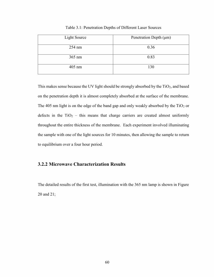
60
Table 3.1: Penetration Depths of Different Laser Sources
Light Source Penetration Depth (μm)
254 nm 0.36
365 nm 0.83
405 nm 130
This makes sense because the UV light should be strongly absorbed by the TiO2, and based
on the penetration depth it is almost completely absorbed at the surface of the membrane.
The 405 nm light is on the edge of the band gap and only weakly absorbed by the TiO2 or
defects in the TiO2 – this means that charge carriers are created almost uniformly
throughout the entire thickness of the membrane. Each experiment involved illuminating
the sample with one of the light sources for 10 minutes, then allowing the sample to return
to equilibrium over a four hour period.
3.2.2 Microwave Characterization Results
The detailed results of the first test, illumination with the 365 nm lamp is shown in Figure
20 and 21;
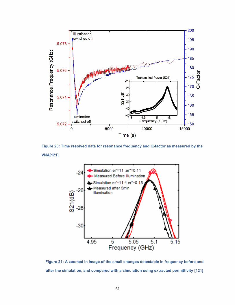
61
Figure 20: Time resolved data for resonance frequency and Q-factor as measured by the
VNA[121]
Figure 21: A zoomed in image of the small changes detectable in frequency before and
after the simulation, and compared with a simulation using extracted permittivity [121]
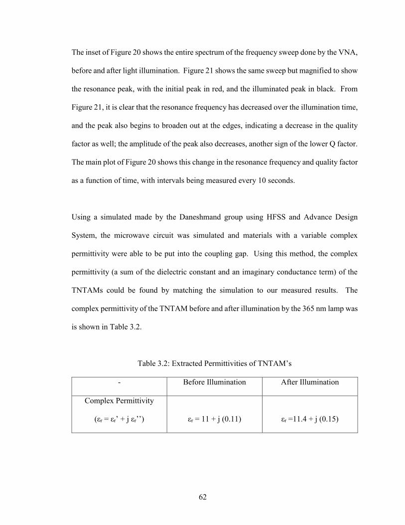
62
The inset of Figure 20 shows the entire spectrum of the frequency sweep done by the VNA,
before and after light illumination. Figure 21 shows the same sweep but magnified to show
the resonance peak, with the initial peak in red, and the illuminated peak in black. From
Figure 21, it is clear that the resonance frequency has decreased over the illumination time,
and the peak also begins to broaden out at the edges, indicating a decrease in the quality
factor as well; the amplitude of the peak also decreases, another sign of the lower Q factor.
The main plot of Figure 20 shows this change in the resonance frequency and quality factor
as a function of time, with intervals being measured every 10 seconds.
Using a simulated made by the Daneshmand group using HFSS and Advance Design
System, the microwave circuit was simulated and materials with a variable complex
permittivity were able to be put into the coupling gap. Using this method, the complex
permittivity (a sum of the dielectric constant and an imaginary conductance term) of the
TNTAMs could be found by matching the simulation to our measured results. The
complex permittivity of the TNTAM before and after illumination by the 365 nm lamp was
is shown in Table 3.2.
Table 3.2: Extracted Permittivities of TNTAM’s
- Before Illumination After Illumination
Complex Permittivity
(εr = εr’ + j εr’’)
εr = 11 + j (0.11)
εr =11.4 + j (0.15)

63
As expected, the dielectric term increased after illumination due to charge carriers being
excited and then trapped in the material. The bound charges left trapped in defect states
within the bandgap are still more polarizable than if they were in the valence band. The
conductance term also increased, indicating that some of those charge carriers remained
untrapped in the material and added to the small current of the microwave circuit. These
two phenomena have opposite effects on the resonant frequency (the former decreases it,
the latter increases it) but the dominant effect is in the dielectric term and so we see a net
decrease in f0. Similarly, the Q factor is increased by the increasing dielectric constant, but
the increase in current leads to more losses in the circuit, and there is a net overall decrease
in Q. These trends are consistent regardless of the light source we use, so long as the light
is absorbed and able to excite charge carriers in the material.
Other useful material parameters can be gained from the excitation and decay curves in
Figure 20. Just like our TOF measurements, we can measure the recombination lifetimes
of charge carriers after the light source has been turned off. Because the time scales are on
the order of minutes to hours, high speed detection equipment is not needed beyond the
speeds of the VNA. It is unlikely that there are any fast decay responses or excitation
responses because those would likely show up as large instantaneous shifts in fo or Q
between two time intervals but none of those are present. Plots of the excitation and decay
curves for the 254 nm and 405 nm experiment are shown in Figure 22 and 23.
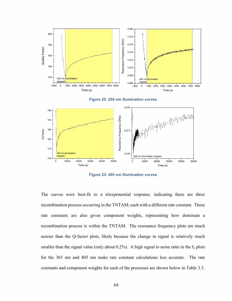
64
Figure 22: 254 nm illumination curves
Figure 23: 405 nm illumination curves
The curves were best-fit to a triexponential response, indicating there are three
recombination process occurring in the TNTAM; each with a different rate constant. These
rate constants are also given component weights, representing how dominant a
recombination process is within the TNTAM. The resonance frequency plots are much
noisier than the Q-factor plots, likely because the change in signal is relatively much
smaller than the signal value (only about 0.2%). A high signal to noise ratio in the fo plots
for the 365 nm and 405 nm make rate constant calculations less accurate. The rate
constants and component weights for each of the processes are shown below in Table 3.3.
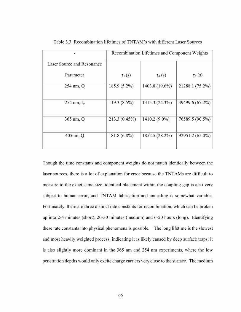
65
Table 3.3: Recombination lifetimes of TNTAM’s with different Laser Sources
- Recombination Lifetimes and Component Weights
Laser Source and Resonance
Parameter
τ1 (s)
τ2 (s)
τ3 (s)
254 nm, Q 185.9 (5.2%)
1403.8 (19.6%)
21288.1 (75.2%)
254 nm, fo 119.3 (8.5%)
1315.3 (24.3%)
39499.6 (67.2%)
365 nm, Q 213.3 (0.45%)
1410.2 (9.0%)
76589.5 (90.5%)
405nm, Q 181.8 (6.8%)
1852.5 (28.2%)
92951.2 (65.0%)
Though the time constants and component weights do not match identically between the
laser sources, there is a lot of explanation for error because the TNTAMs are difficult to
measure to the exact same size, identical placement within the coupling gap is also very
subject to human error, and TNTAM fabrication and annealing is somewhat variable.
Fortunately, there are three distinct rate constants for recombination, which can be broken
up into 2-4 minutes (short), 20-30 minutes (medium) and 6-20 hours (long). Identifying
these rate constants into physical phenomena is possible. The long lifetime is the slowest
and most heavily weighted process, indicating it is likely caused by deep surface traps; it
is also slightly more dominant in the 365 nm and 254 nm experiments, where the low
penetration depths would only excite charge carriers very close to the surface. The medium
66
and short lifetime is thought to be electrons and holes being trapped in shallower traps of
two distinct energies, resulting in two different rates.
3.2.3 Discussion
Time resolved microwave conductivity is a useful and relatively newer method for
characterizing material parameters in the low frequency microwave regime. This was a
fruitful partnership with the Daneshmand group because it gave us a use for the
delaminated TiO2 membranes and the complex permittivity ended up having strong
response to the UV light, showing the unique abilities of the microwave resonators. The
methods developed for these TRMC experiments are much easier to set up, manipulate the
sample, and record data than previous experiments using a cavity waveguide resonator,
which is bulky and hard to use.
TiO2 membranes were characterized using the TRMC method and we found that the
complex permittivity could be accurately found using the ADS simulations matched with
our experiments. The transient data was used to measure the long-lived charge
recombination lifetimes in the TNTAMs, and evidence suggests that the triexponential
lifetime is evidence of deep surface traps (common on TiO2 nanostructures), as well as
more shallow traps with faster recombination.
There is also a lot of room for the planar microwave resonators to grow. As an example,
the quality factor has been increased in newer resonators; and the sharper peaks make minor
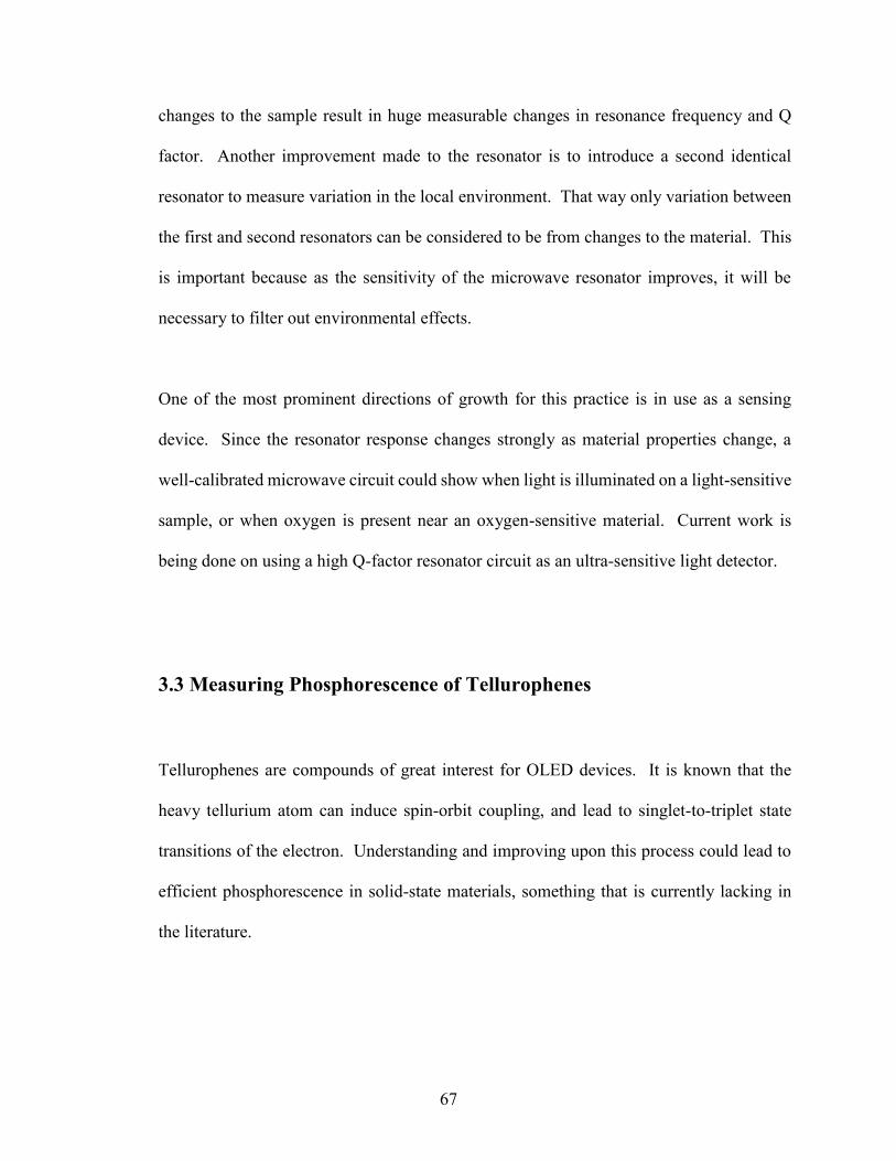
67
changes to the sample result in huge measurable changes in resonance frequency and Q
factor. Another improvement made to the resonator is to introduce a second identical
resonator to measure variation in the local environment. That way only variation between
the first and second resonators can be considered to be from changes to the material. This
is important because as the sensitivity of the microwave resonator improves, it will be
necessary to filter out environmental effects.
One of the most prominent directions of growth for this practice is in use as a sensing
device. Since the resonator response changes strongly as material properties change, a
well-calibrated microwave circuit could show when light is illuminated on a light-sensitive
sample, or when oxygen is present near an oxygen-sensitive material. Current work is
being done on using a high Q-factor resonator circuit as an ultra-sensitive light detector.
3.3 Measuring Phosphorescence of Tellurophenes
Tellurophenes are compounds of great interest for OLED devices. It is known that the
heavy tellurium atom can induce spin-orbit coupling, and lead to singlet-to-triplet state
transitions of the electron. Understanding and improving upon this process could lead to
efficient phosphorescence in solid-state materials, something that is currently lacking in
the literature.
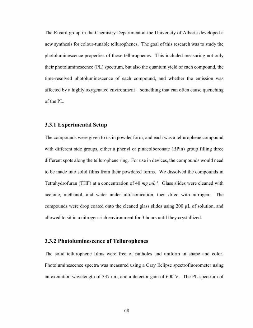
68
The Rivard group in the Chemistry Department at the University of Alberta developed a
new synthesis for colour-tunable tellurophenes. The goal of this research was to study the
photoluminescence properties of those tellurophenes. This included measuring not only
their photoluminescence (PL) spectrum, but also the quantum yield of each compound, the
time-resolved photoluminescence of each compound, and whether the emission was
affected by a highly oxygenated environment – something that can often cause quenching
of the PL.
3.3.1 Experimental Setup
The compounds were given to us in powder form, and each was a tellurophene compound
with different side groups, either a phenyl or pinacolboronate (BPin) group filling three
different spots along the tellurophene ring. For use in devices, the compounds would need
to be made into solid films from their powdered forms. We dissolved the compounds in
Tetrahydrofuran (THF) at a concentration of 40 mg mL-1. Glass slides were cleaned with
acetone, methanol, and water under ultrasonication, then dried with nitrogen. The
compounds were drop coated onto the cleaned glass slides using 200 μL of solution, and
allowed to sit in a nitrogen-rich environment for 3 hours until they crystallized.
3.3.2 Photoluminescence of Tellurophenes
The solid tellurophene films were free of pinholes and uniform in shape and color.
Photoluminescence spectra was measured using a Cary Eclipse spectrofluorometer using
an excitation wavelength of 337 nm, and a detector gain of 600 V. The PL spectrum of
69
each compound is shown below in Figure 24 and 25, with an inset of their chemical
structure.
Figure 24: The two most photoluminescent compounds of the batch, Ph2-Green and Ph2-
yellow [102]
Figure 25: The remaining three compounds made by the Rivard group, they are all
showing emission around 530 nm, but much less than the other two compounds. Adapted
from [102]
70
The tellurophene samples show emission between 500 and 600 nm. This is a wide range
of colour-tunability compared to previous reports in the literature. The two most
photoluminescent films were the 2,5-BPin2-3,5-Ph2-Te (Ph2-Green) and 2,4-BPin2-3,5-
Ph2-Te (Ph2-Yellow). The Benzo-Te-BPin-Ph molecule was strongly photoluminescent
in THF:water (5:95) solution, but much less so in solid state; this indicates aggregation
induced quenching occurs in some of the materials but not others. Alternatively, the
Benzo-Te-BPin2 was weakly emissive in solution, but showed a strong photoluminescence
signal in the solid state, indicating crystallization-induced emission. The Benzo-Te-Ph2
was weakly emissive in both solid state and solution, which means that a BPin group is
likely necessary for strong photoluminescence, the necessity of the BPin group is
something that has been seen previously in the literature.
After fabrication of the tellurophene samples, we did not keep them in a nitrogen rich
environment for our initial tests. Therefore the compounds are shown to maintain
photoluminescence over a period of a few days. A high intensity light test was done later
and it showed that the organic Ph2-Green is stable even under direct illumination by a
180W sodium lamp, whereas less stable thiophenes lost their emission after about 5
minutes of exposure and this result is shown in Figure 26.

71
Figure 26: Ph2-Green maintains its original emission after exposure to high heat and light
intensity, Dihexylquaterthiophene, a known photoluminescent material breaks down[102]
Quantifying the photoluminescence requires additional scans and a different scanning
procedure that will ensure all of the emitted light is accounted for. We use the method
designed by Friend et al. [119]which uses an integrating sphere to prevent any light being
lost to the environment once it has entered the system. The quantum yield represents the
ratio of light emitted to light absorbed by a material, so we run a series of measurements
described in section 2.3.5 and use the data with equation 10. The results of the quantum
yield measurements are shown below in Table 3.4.
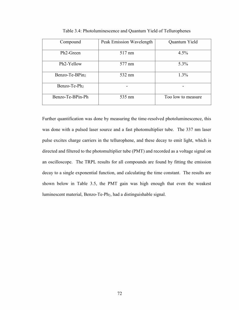
72
Table 3.4: Photoluminescence and Quantum Yield of Tellurophenes
Compound Peak Emission Wavelength Quantum Yield
Ph2-Green 517 nm 4.5%
Ph2-Yellow 577 nm 5.3%
Benzo-Te-BPin2 532 nm 1.3%
Benzo-Te-Ph2 - -
Benzo-Te-BPin-Ph 535 nm Too low to measure
Further quantification was done by measuring the time-resolved photoluminescence, this
was done with a pulsed laser source and a fast photomultiplier tube. The 337 nm laser
pulse excites charge carriers in the tellurophene, and these decay to emit light, which is
directed and filtered to the photomultiplier tube (PMT) and recorded as a voltage signal on
an oscilloscope. The TRPL results for all compounds are found by fitting the emission
decay to a single exponential function, and calculating the time constant. The results are
shown below in Table 3.5, the PMT gain was high enough that even the weakest
luminescent material, Benzo-Te-Ph2, had a distinguishable signal.

73
Table 3.5: Photoluminescence Lifetime of Tellurophenes
Compound Photoluminescence Lifetime
(μs)
Ph2-Green 51.7
Ph2-Yellow 17.9
Benzo-Te-BPin2 6.1
Benzo-Te-Ph2 9.6
Benzo-Te-BPin-Ph 59.3
These lifetimes are all in the nanosecond range, indicating that each compound studied
exhibits primarily phosphorescence. A fast emission was also detected for these
compounds but it did not align with the expected PL spectrum and was most likely
electronic noise from the laser pulse being picked up by the PMT, or it could have been the
laser pulse being incompletely filtered by the monochromator. The lifetime data correlates
well with the quantum yield data, and the phosphorescence of the samples can explain why
the quantum yield may be difficult to increase. As expected, phosphorescent materials
have a low quantum yield because their long lifetime makes carriers susceptible to
quenching or non-radiative recombination over longer time periods.
Interestingly, the effect of oxygen quenching with these compounds was found to be
already quite limited. Oxygen quenching is often a major source of loss in phosphorescent
materials so it was investigated as a source of loss in our materials. This was done by
testing 3 different environments for the tellurophenes. First, the Ph2-Green film was made
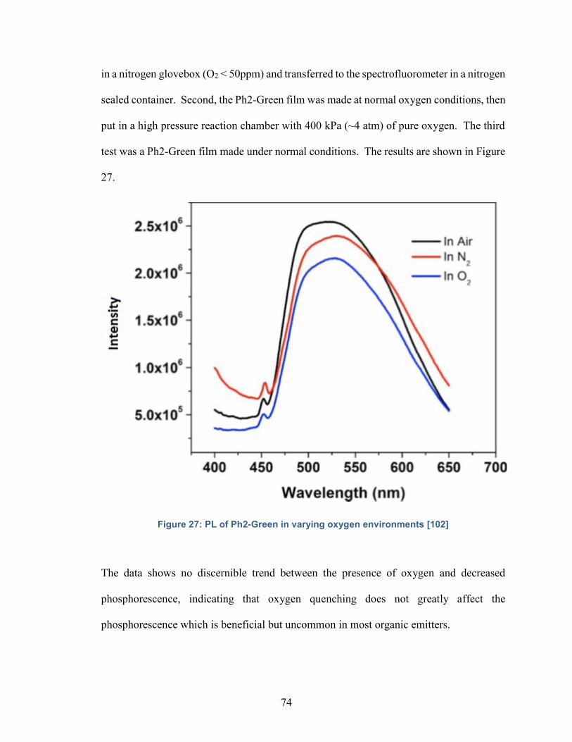
74
in a nitrogen glovebox (O2 < 50ppm) and transferred to the spectrofluorometer in a nitrogen
sealed container. Second, the Ph2-Green film was made at normal oxygen conditions, then
put in a high pressure reaction chamber with 400 kPa (~4 atm) of pure oxygen. The third
test was a Ph2-Green film made under normal conditions. The results are shown in Figure
27.
Figure 27: PL of Ph2-Green in varying oxygen environments [102]
The data shows no discernible trend between the presence of oxygen and decreased
phosphorescence, indicating that oxygen quenching does not greatly affect the
phosphorescence which is beneficial but uncommon in most organic emitters.

75
3.3.3 Discussion
The photoluminescence of the tellurophenes provided by the Rivard group was unique for
many reasons. First, the photoluminescence was tunable by changing the functional groups
on the tellurophene ring; and this was accomplished with only minor changes in chemical
synthesis. Second, using the methods developed by Friend et al. we found the quantum
yield to be quite low. This was later found to be a likely consequence of the phosphorescent
nature of the tellurophene emission, which we found from an analysis of the emission
lifetimes.
The phosphorescence was also unaffected by oxygen in the environment, indicating that
oxygen quenching is not a pathway of loss for the Ph2-Green tellurophene. This will likely
make the tellurophenes a key area of interest for OLED or biological marking applications.
While improvements made to the tellurophene compounds are out of my expertise it is
likely that even the materials presented above, specifically the Ph2-Green and Ph2-Yellow,
could be useful in light emitting devices or applications as they are shown.
3.4 Charge Carrier Dynamics of Tellurophenes
Due to the unique photoluminescence properties of the tellurophenes, it makes sense to
further characterize their material properties for potential device applications. In this
section, the charge carrier dynamics of tellurophenes provided by the Rivard group are

76
studied. With adequate charge transport, the environmental stability of tellurophenes
combined with their colour tenability could make them very useful as OLEDs.
3.4.1 Experimental Setup
The tellurophene provided by Dr. Rivard was known as B-6-Te-B, it is a tellurophene
compound with two BPin side groups. We made multiple films by dissolving 40 mgmL-1
of the compound in THF and drop-coating it onto cleaned FTO or spin coating it onto
cleaned FTO at 2000 rpm. The powder was also thermally evaporated into a film using a
PVD-75 organics evaporator. The chemical structure and optical properties of the three
films are shown in Figure 28.
Figure 28: The chemical structure of B-6-Te-B (A) and its absorbance (B) and
photoluminescence (C) in solid state. [101]
The photoluminescence spectra and the UV-Vis absorption spectra show that the drop-
coated film has the highest PL peak at 500-550 nm and the highest absorbance. This
indicates that the drop-coated film is the most crystalline. The absorbance plot shows that
77
the drop-coated film will absorb below ~375 nm, and the excitation wavelength for PL was
set to be 350 nm. Below 320 nm the light is absorbed by the FTO and using an excitation
signal below this value could skew the PL results.
3.4.2 Photoluminescence and Charge Transport Results
By using the same methods from section 3.3.2, we collected a quantum yield and emission
lifetime for the drop-coated tellurophene samples. The quantum yield was found to be
11.5% and the emission lifetime was measured at 18 μs. This puts the B-6-Te-B
tellurophene well within the class of phosphorescent tellurophenes; and it has a relatively
high quantum yield. The tellurophene compound is also very stable in ambient
atmosphere; and it maintained its photoluminescence even after years of initial fabrication,
something that is very uncommon in organic phosphorescent materials.
An experiment called Time-Resolved Dark Injection (TRDI) was done to quantify the
charge transport capabilities of the B-6-Te-B compound. This uses the pulse mode on the
Keithley Semiconductor Parameter Analyzer by creating a large current pulse at one side
of the sample at a specified time and measuring the collection of the current on the other
side[125]. Dark injection is similar to time of flight in that it is a method to find the
mobility of the charge carriers, and each respective method has its own advantages and
disadvantages. TOF was done on these samples but the signal was too broad and a transit
time could not be calculated. The light was either not absorbed in a small enough
penetration depth, the dielectric relaxation time of the material was too fast, or re-emission

78
of the light was absorbed by defects or dopants and caused significant signal dispersion.
The former is the most likely problem, as the dielectric relaxation time of these organics is
expected to be slow because of their mediocre conductivity; and re-emission of light
causing signal dispersion would likely show up in the dark injection measurements, which
was not the case. Dark injection was able to measure the transit time in this case because
it does not rely on material absorption but rather a voltage pulse to inject excess carriers
into the material. Because of the similarity of the two methods; equation 4 still applies and
was used to calculate a hole mobility of 1.1 × 10⁻⁴𝑐𝑚2𝑉−1𝑠−1. The electron mobility
was difficult to calculate because the Keithley pulse mode was not able to measure a long
enough time interval, that can at least be used to estimate the electron mobility as being
less than 10−6𝑐𝑚2𝑉−1𝑠−1. The hole mobility of the drop coated film is orders of
magnitude higher than for the spin-coated or thermally evaporated film, indicating the film
crystallinity has a large effect on the charge transport.
3.4.3 Discussion
We completed a series of experiments to see the potential of the B-6-Te-B tellurophene
compounds for use in electronic devices. The B-6-Te-B was similar to the other
tellurophenes of section 3.3 in that it had a long emission lifetime, a relatively high
quantum yield, and exceptional stability. The hole mobility was adequate in the drop-
coated film, and it would be ideal to make prototype OLEDs using these methods. It would
also be interesting to use cathodoluminescence tests on all of these materials, in order to
see the effectiveness of injected electrons in creating light emission.

79
Due to limitations in material preparation, all of the tellurophenes could not be
characterized, especially since we needed about 10 mg of the powder for each film we
made. Other potential candidates for OLEDs would be the Ph2-Green and Ph2-Yellow
compounds but we were not able to test their charge transport, though we already know
they have excellent PL properties and stability.
80
Chapter 4: Conclusion and Future Research Directions
This work focused on measuring carrier dynamics (inclusive of photoluminescence) in two
different semiconducting material systems, namely TiO2 nanostructures and organic
tellurophenes. Optoelectronic characterization of these material systems is important,
especially for use in electronic devices, and it is necessary to know the material properties
in order to use them most effectively for applications.
Anatase-phase TiO2 nanoparticles and polycrystalline thin films are popular electron
transport layers in devices such as perovskite solar cells and OLEDs, and are also
commonly used in gas and UV sensing. It remains to be seen if TiO2 nanotubes and
nanowires become as technologically significant as other forms of TiO2. As a transport
layer, TiO2 nanowires were shown to have very low mobility compared to bulk TiO2 due
to a high density of deep traps on the surface of the nanowires. The TOF and IV analysis
involved in this discovery are not commonly used, but they can prove very useful for
understanding differences between nanostructures and bulk materials, especially when it
comes to traps. We were able to passivate the deep traps using an ODPA SAM and improve
the carrier mobility by a factor of almost 1000.
10-100μm thick free-standing TiO2 nanotube membranes are of great interest for
macromolecule filtration, drug delivery, substrates for cell cultures and substrate-assisted
laser induced desorption mass spectrometry (SALDI) but it was not until their use in
microwave sensing that they had a niche optoelectronic application. The goal of the TRMC
81
work was to characterize the transient complex permittivity of TiO2 nanotubes during
exposure to UV light and shed light on the underlying carrier dynamics. While there had
been several papers to measure the microwave conductivity in TiO2 thin films and
nanoparticles using conventional cavity waveguide resonators, there were almost no
reports that used planar microwave resonators. Planar microwave resonators are not merely
compact, inexpensive and easier to fabricate, but also offer profound advantages in terms
of the orders of magnitude higher Q-factors possible, the ability to easily monitor both the
real and imaginary parts of the complex permittivity, the ability to apply both DC bias and
illumination at the same time, and also the opportunity to introduce custom ambients during
the measurement of the microwave response. In the process of performing the microwave
characterization of titania nanotube membranes, it was found that the principles of TRMC
could easily be applied to sensing applications, and the TiO2-UV light dynamic was just
one of many material-environment interactions that could be tracked using this method.
Future work in this project can proceed in either one of two major directions; a more
comprehensive characterization of material permittivity in the microwave to terahertz
frequency regime, or improving the experimental methods so the system can function as
an accurate and selective sensor for analytes such as light, small molecules, metal ions, and
biomolecules. There is significant work that can be done in this field on both the material
side and the sensing side.
The organic tellurophenes were studied because they had new and interesting color
tunability in an organic tellurophene molecule, something which is often non-radiative. In
order to further explore the results, it was necessary to setup quantitative tests that could
82
accurately describe this new photoluminescence such as quantum yield and time resolved
photoluminescence. This proved to be effective because each test gave us more insight
into the nature of the compounds. The materials were all phosphorescent with a lifetime
in the range of 10 μs, the more strongly emitting ones having a relatively high quantum
yield around 5%. The BPin group that had been previously suggested as being necessary
for emission was again shown to be necessary. There was also evidence of crystallization
induced phosphorescence in the Benzo-Te-BPin2, which is in line with when we found that
high crystallinity is a huge factor in emission intensity for the B-6-Te-B compound in
section 3.4. The compounds also showed no signs of degradation over time, or when
exposed to high light intensity, or when kept in a high oxygen environment; all things that
are common issues for organic light emitters. The tellurophenes showed such interesting
PL properties that their charge transport was measured with the goal being to really see the
potential of these materials in OLEDs. The hole mobility measurement of 1.1 ×
10−4𝑐𝑚2𝑉−1𝑠−1 indicates it could be possible, but a prototype has not yet been made.
Further study is probably necessary before their use in devices, but these materials are so
luminescent and stable that their use in devices should continue to be investigated.
83
References
[1] R. P. Feynman, "There's plenty of room at the bottom," Engineering and science, vol. 23,
pp. 22-36, 1960.
[2] T. V. Duncan, "Applications of nanotechnology in food packaging and food safety:
barrier materials, antimicrobials and sensors," Journal of colloid and interface science,
vol. 363, pp. 1-24, 2011.
[3] R. K. Sastry, S. Anshul, and N. Rao, "Nanotechnology in food processing sector-An
assessment of emerging trends," Journal of food science and technology, vol. 50, pp.
831-841, 2013.
[4] X. He and H.-M. Hwang, "Nanotechnology in food science: Functionality, applicability,
and safety assessment," journal of food and drug analysis, vol. 24, pp. 671-681, 2016.
[5] Y. Liu, X. Chen, and J. Xin, "Super-hydrophobic surfaces from a simple coating method:
a bionic nanoengineering approach," Nanotechnology, vol. 17, p. 3259, 2006.
[6] S.-M. Lee and T. H. Kwon, "Mass-producible replication of highly hydrophobic surfaces
from plant leaves," Nanotechnology, vol. 17, p. 3189, 2006.
[7] J. Pan, X. Song, J. Zhang, H. Shen, and Q. Xiong, "Switchable wettability in SnO2
nanowires and SnO2@ SnO2 heterostructures," The Journal of Physical Chemistry C,
vol. 115, pp. 22225-22231, 2011.
[8] G. Thilagavathi, A. Raja, and T. Kannaian, "Nanotechnology and protective clothing for
defence personnel," Defence Science Journal, vol. 58, p. 451, 2008.
[9] L. Lo, Y. Li, K. Yeung, and C. Yuen, "Indicating the development stage of
nanotechnology in the textile and clothing industry," International Journal of
Nanotechnology, vol. 4, pp. 667-679, 2007.
[10] K. Arivalagan, S. Ravichandran, K. Rangasamy, and E. Karthikeyan, "Nanomaterials and
its potential applications," International journal of chemtech research, vol. 3, pp. 534-
538, 2011.
[11] G. Shen, P.-C. Chen, K. Ryu, and C. Zhou, "Devices and chemical sensing applications
of metal oxide nanowires," Journal of Materials Chemistry, vol. 19, pp. 828-839, 2009.
[12] Y. Li, F. Della Valle, M. Simonnet, I. Yamada, and J.-J. Delaunay, "High-performance
UV detector made of ultra-long ZnO bridging nanowires," Nanotechnology, vol. 20, p.
045501, 2008.
[13] M.-W. Ahn, K.-S. Park, J.-H. Heo, J.-G. Park, D.-W. Kim, K. J. Choi, et al., "Gas
sensing properties of defect-controlled ZnO-nanowire gas sensor," Applied physics
letters, vol. 93, p. 263103, 2008.
[14] J. Wilkinson, "Nanotechnology applications in medicine," Medical device technology,
vol. 14, pp. 29-31, 2003.
[15] G. Balasundaram and T. J. Webster, "Nanotechnology and biomaterials for orthopedic
medical applications," 2006.
[16] S. Prabhu and E. K. Poulose, "Silver nanoparticles: mechanism of antimicrobial action,
synthesis, medical applications, and toxicity effects," International Nano Letters, vol. 2,
p. 32, 2012.
[17] W.-N. Wang, W.-J. An, B. Ramalingam, S. Mukherjee, D. M. Niedzwiedzki, S.
Gangopadhyay, et al., "Size and structure matter: enhanced CO2 photoreduction
84
efficiency by size-resolved ultrafine Pt nanoparticles on TiO2 single crystals," Journal of
the American Chemical Society, vol. 134, pp. 11276-11281, 2012.
[18] M. Paulose, O. K. Varghese, G. K. Mor, C. A. Grimes, and K. G. Ong, "Unprecedented
ultra-high hydrogen gas sensitivity in undoped titania nanotubes," Nanotechnology, vol.
17, p. 398, 2005.
[19] F. Dong, W. Zhao, and Z. Wu, "Characterization and photocatalytic activities of C, N and
S co-doped TiO2 with 1D nanostructure prepared by the nano-confinement effect,"
Nanotechnology, vol. 19, p. 365607, 2008.
[20] Y.-M. Chien, F. Lefevre, I. Shih, and R. Izquierdo, "A solution processed top emission
OLED with transparent carbon nanotube electrodes," Nanotechnology, vol. 21, p.
134020, 2010.
[21] S. Jha, J.-C. Qian, O. Kutsay, J. Kovac Jr, C.-Y. Luan, J. A. Zapien, et al., "Violet-blue
LEDs based on p-GaN/n-ZnO nanorods and their stability," Nanotechnology, vol. 22, p.
245202, 2011.
[22] T.-H. Han, Y. Lee, M.-R. Choi, S.-H. Woo, S.-H. Bae, B. H. Hong, et al., "Extremely
efficient flexible organic light-emitting diodes with modified graphene anode," Nature
Photonics, vol. 6, pp. 105-110, 2012.
[23] T. Stelzner, M. Pietsch, G. Andrä, F. Falk, E. Ose, and S. Christiansen, "Silicon
nanowire-based solar cells," Nanotechnology, vol. 19, p. 295203, 2008.
[24] K. Shankar, G. K. Mor, H. E. Prakasam, S. Yoriya, M. Paulose, O. K. Varghese, et al.,
"Highly-ordered TiO2 nanotube arrays up to 220 µm in length: use in water
photoelectrolysis and dye-sensitized solar cells," Nanotechnology, vol. 18, p. 065707,
2007.
[25] H.-S. Kim, J.-W. Lee, N. Yantara, P. P. Boix, S. A. Kulkarni, S. Mhaisalkar, et al., "High
efficiency solid-state sensitized solar cell-based on submicrometer rutile TiO2 nanorod
and CH3NH3PbI3 perovskite sensitizer," Nano letters, vol. 13, pp. 2412-2417, 2013.
[26] X. Rocquefelte, F. Goubin, H.-J. Koo, M.-H. Whangbo, and S. Jobic, "Investigation of
the origin of the empirical relationship between refractive index and density on the basis
of first principles calculations for the refractive indices of various TiO2 phases,"
Inorganic chemistry, vol. 43, pp. 2246-2251, 2004.
[27] D. O. Scanlon, C. W. Dunnill, J. Buckeridge, S. A. Shevlin, A. J. Logsdail, S. M.
Woodley, et al., "Band alignment of rutile and anatase TiO2," Nature materials, vol. 12,
pp. 798-801, 2013.
[28] J. Zhang, P. Zhou, J. Liu, and J. Yu, "New understanding of the difference of
photocatalytic activity among anatase, rutile and brookite TiO2," Physical Chemistry
Chemical Physics, vol. 16, pp. 20382-20386, 2014.
[29] H. Park, Y. Park, W. Kim, and W. Choi, "Surface modification of TiO 2 photocatalyst for
environmental applications," Journal of Photochemistry and Photobiology C:
Photochemistry Reviews, vol. 15, pp. 1-20, 2013.
[30] Y. Xie, L. Wei, Q. Li, Y. Chen, S. Yan, J. Jiao, et al., "High-performance self-powered
UV photodetectors based on TiO2 nano-branched arrays," Nanotechnology, vol. 25, p.
075202, 2014.
[31] Y. Zhao and K. Zhu, "Charge transport and recombination in perovskite (CH3NH3) PbI3
sensitized TiO2 solar cells," The Journal of Physical Chemistry Letters, vol. 4, pp. 2880-
2884, 2013.
85
[32] W.-Q. Wu, B.-X. Lei, H.-S. Rao, Y.-F. Xu, Y.-F. Wang, C.-Y. Su, et al., "Hydrothermal
fabrication of hierarchically anatase TiO2 nanowire arrays on FTO glass for dye-
sensitized solar cells," Scientific reports, vol. 3, p. 1352, 2013.
[33] B. A. Al-Asbahi, M. H. Haji Jumali, and M. S. AlSalhi, "Enhanced Optoelectronic
Properties of PFO/Fluorol 7GA Hybrid Light Emitting Diodes via Additions of TiO2
Nanoparticles," Polymers, vol. 8, p. 334, 2016.
[34] R. Fateh, R. Dillert, and D. Bahnemann, "Self-Cleaning properties, mechanical stability,
and adhesion strength of transparent photocatalytic TiO2–ZnO coatings on
polycarbonate," ACS applied materials & interfaces, vol. 6, pp. 2270-2278, 2014.
[35] C. Sotelo-Vazquez, N. Noor, A. Kafizas, R. Quesada-Cabrera, D. O. Scanlon, A. Taylor,
et al., "Multifunctional P-doped TiO2 films: a new approach to self-cleaning, transparent
conducting oxide materials," Chemistry of Materials, vol. 27, pp. 3234-3242, 2015.
[36] A. M. Zaky and B. P. Chaplin, "Porous substoichiometric TiO2 anodes as reactive
electrochemical membranes for water treatment," Environmental science & technology,
vol. 47, pp. 6554-6563, 2013.
[37] G. Ghasemzadeh, M. Momenpour, F. Omidi, M. R. Hosseini, M. Ahani, and A.
Barzegari, "Applications of nanomaterials in water treatment and environmental
remediation," Frontiers of Environmental Science & Engineering, vol. 8, pp. 471-482,
2014.
[38] H. Xu, S. Ouyang, P. Li, T. Kako, and J. Ye, "High-active anatase TiO2 nanosheets
exposed with 95%{100} facets toward efficient H2 evolution and CO2 photoreduction,"
ACS applied materials & interfaces, vol. 5, pp. 1348-1354, 2013.
[39] D. Reyes-Coronado, G. Rodríguez-Gattorno, M. Espinosa-Pesqueira, C. Cab, R. d. de
Coss, and G. Oskam, "Phase-pure TiO2 nanoparticles: anatase, brookite and rutile,"
Nanotechnology, vol. 19, p. 145605, 2008.
[40] H. G. Yang and H. C. Zeng, "Preparation of hollow anatase TiO2 nanospheres via
Ostwald ripening," The Journal of Physical Chemistry B, vol. 108, pp. 3492-3495, 2004.
[41] H. Li, Y. Zeng, T. Huang, L. Piao, Z. Yan, and M. Liu, "Hierarchical TiO2 nanospheres
with dominant {001} facets: facile synthesis, growth mechanism, and photocatalytic
activity," Chemistry–A European Journal, vol. 18, pp. 7525-7532, 2012.
[42] C. A. Grimes and G. K. Mor, TiO2 nanotube arrays: synthesis, properties, and
applications: Springer Science & Business Media, 2009.
[43] P. Roy, S. Berger, and P. Schmuki, "TiO2 nanotubes: synthesis and applications,"
Angewandte Chemie International Edition, vol. 50, pp. 2904-2939, 2011.
[44] C. A. Grimes, "Synthesis and application of highly ordered arrays of TiO 2 nanotubes,"
Journal of Materials Chemistry, vol. 17, pp. 1451-1457, 2007.
[45] Z. Miao, D. Xu, J. Ouyang, G. Guo, X. Zhao, and Y. Tang, "Electrochemically induced
sol− gel preparation of single-crystalline TiO2 nanowires," Nano Letters, vol. 2, pp. 717-
720, 2002.
[46] Y. Zhang, G. Li, Y. Jin, Y. Zhang, J. Zhang, and L. Zhang, "Hydrothermal synthesis and
photoluminescence of TiO 2 nanowires," Chemical Physics Letters, vol. 365, pp. 300-
304, 2002.
[47] J.-N. Nian and H. Teng, "Hydrothermal synthesis of single-crystalline anatase TiO2
nanorods with nanotubes as the precursor," The Journal of Physical Chemistry B, vol.
110, pp. 4193-4198, 2006.
86
[48] B. Liu and E. S. Aydil, "Growth of oriented single-crystalline rutile TiO2 nanorods on
transparent conducting substrates for dye-sensitized solar cells," Journal of the American
Chemical Society, vol. 131, pp. 3985-3990, 2009.
[49] P. D. Cozzoli, A. Kornowski, and H. Weller, "Low-temperature synthesis of soluble and
processable organic-capped anatase TiO2 nanorods," Journal of the American Chemical
Society, vol. 125, pp. 14539-14548, 2003.
[50] C. Cao, C. Hu, X. Wang, S. Wang, Y. Tian, and H. Zhang, "UV sensor based on TiO 2
nanorod arrays on FTO thin film," Sensors and Actuators B: Chemical, vol. 156, pp. 114-
119, 2011.
[51] J. Zhang, M. Li, Z. Feng, J. Chen, and C. Li, "UV Raman spectroscopic study on TiO2. I.
Phase transformation at the surface and in the bulk," The Journal of Physical Chemistry
B, vol. 110, pp. 927-935, 2006.
[52] R. D. Shannon, "Phase Transformation Studies in TiO2 Supporting Different Defect
Mechanisms in Vacuum‐Reduced and Hydrogen‐Reduced Rutile," Journal of Applied
Physics, vol. 35, pp. 3414-3416, 1964.
[53] M. Kong, Y. Li, X. Chen, T. Tian, P. Fang, F. Zheng, et al., "Tuning the relative
concentration ratio of bulk defects to surface defects in TiO2 nanocrystals leads to high
photocatalytic efficiency," Journal of the American Chemical Society, vol. 133, pp.
16414-16417, 2011.
[54] E. Logothetis and R. E. Hetrick, "Oscillations in the electrical resistivity of TiO2 induced
by solid/gas interactions," Solid State Communications, vol. 31, pp. 167-171, 1979.
[55] F. Cardon, "Polarization and space-charge-limited currents in rutile (TiO2)," Physica,
vol. 27, pp. 841-849, 1961.
[56] E. Hendry, M. Koeberg, B. O'regan, and M. Bonn, "Local field effects on electron
transport in nanostructured TiO2 revealed by terahertz spectroscopy," Nano letters, vol.
6, pp. 755-759, 2006.
[57] I. Abayev, A. Zaban, F. Fabregat-Santiago, and J. Bisquert, "Electronic conductivity in
nanostructured TiO2 films permeated with electrolyte," PHYSICA STATUS SOLIDI A
APPLIED RESEARCH, vol. 196, pp. R4-R6, 2003.
[58] M. Dolata, P. Kedzierzawski, and J. Augustynski, "Comparative impedance spectroscopy
study of rutile and anatase TiO2 film electrodes," Electrochimica Acta, vol. 41, pp. 1287-
1293, 1996.
[59] P. De Jongh and D. Vanmaekelbergh, "Investigation of the electronic transport properties
of nanocrystalline particulate TiO2 electrodes by intensity-modulated photocurrent
spectroscopy," The Journal of Physical Chemistry B, vol. 101, pp. 2716-2722, 1997.
[60] H. Tang, K. Prasad, R. Sanjines, P. Schmid, and F. Levy, "Electrical and optical
properties of TiO2 anatase thin films," Journal of Applied Physics, vol. 75, pp. 2042-
2047, 1994.
[61] J. Van de Lagemaat and A. Frank, "Nonthermalized electron transport in dye-sensitized
nanocrystalline TiO2 films: transient photocurrent and random-walk modeling studies,"
The Journal of Physical Chemistry B, vol. 105, pp. 11194-11205, 2001.
[62] R. G. Breckenridge and W. R. Hosler, "Electrical properties of titanium dioxide
semiconductors," Physical Review, vol. 91, p. 793, 1953.
[63] D. Pan, N. Zhao, Q. Wang, S. Jiang, X. Ji, and L. An, "Facile synthesis and
characterization of luminescent TiO2 nanocrystals," Advanced materials, vol. 17, pp.
1991-1995, 2005.
87
[64] D. M. King, X. Du, A. S. Cavanagh, and A. W. Weimer, "Quantum confinement in
amorphous TiO2 films studied via atomic layer deposition," Nanotechnology, vol. 19, p.
445401, 2008.
[65] E. Baldini, L. Chiodo, A. Dominguez, M. Palummo, S. Moser, M. Yazdi-Rizi, et al.,
"Strongly bound excitons in anatase TiO2 single crystals and nanoparticles," Nature
Communications, vol. 8, 2017.
[66] E.-Z. Tan, P.-G. Yin, T.-t. You, H. Wang, and L. Guo, "Three dimensional design of
large-scale TiO2 nanorods scaffold decorated by silver nanoparticles as SERS sensor for
ultrasensitive malachite green detection," ACS applied materials & interfaces, vol. 4, pp.
3432-3437, 2012.
[67] T.-S. Kang, A. P. Smith, B. E. Taylor, and M. F. Durstock, "Fabrication of highly-
ordered TiO2 nanotube arrays and their use in dye-sensitized solar cells," Nano letters,
vol. 9, pp. 601-606, 2009.
[68] I. Bannat, K. Wessels, T. Oekermann, J. Rathousky, D. Bahnemann, and M. Wark,
"Improving the photocatalytic performance of mesoporous titania films by modification
with gold nanostructures," Chemistry of Materials, vol. 21, pp. 1645-1653, 2009.
[69] S. Farsinezhad, H. Sharma, and K. Shankar, "Interfacial band alignment for
photocatalytic charge separation in TiO 2 nanotube arrays coated with CuPt
nanoparticles," Physical Chemistry Chemical Physics, vol. 17, pp. 29723-29733, 2015.
[70] D. R. Baker and P. V. Kamat, "Photosensitization of TiO2 nanostructures with CdS
quantum dots: particulate versus tubular support architectures," Advanced Functional
Materials, vol. 19, pp. 805-811, 2009.
[71] K. Zhu, N. R. Neale, A. Miedaner, and A. J. Frank, "Enhanced charge-collection
efficiencies and light scattering in dye-sensitized solar cells using oriented TiO2
nanotubes arrays," Nano letters, vol. 7, pp. 69-74, 2007.
[72] J. Jiang, F. Gu, W. Shao, and C. Li, "Fabrication of spherical multi-hollow TiO2
nanostructures for photoanode film with enhanced light-scattering performance,"
Industrial & Engineering Chemistry Research, vol. 51, pp. 2838-2845, 2012.
[73] M. A. Lampert, "Simplified theory of space-charge-limited currents in an insulator with
traps," Physical Review, vol. 103, p. 1648, 1956.
[74] A. Rose, "Space-charge-limited currents in solids," Physical Review, vol. 97, p. 1538,
1955.
[75] A. Many and G. Rakavy, "Theory of transient space-charge-limited currents in solids in
the presence of trapping," Physical Review, vol. 126, p. 1980, 1962.
[76] Y. Zhu and L. Ang, "Analytical re-derivation of space charge limited current in solids
using capacitor model," Journal of Applied Physics, vol. 110, p. 094514, 2011.
[77] J. C. Love, L. A. Estroff, J. K. Kriebel, R. G. Nuzzo, and G. M. Whitesides, "Self-
assembled monolayers of thiolates on metals as a form of nanotechnology," Chemical
reviews, vol. 105, pp. 1103-1170, 2005.
[78] S. Brandriss and S. Margel, "Synthesis and characterization of self-assembled
hydrophobic monolayer coatings on silica colloids," Langmuir, vol. 9, pp. 1232-1240,
1993.
[79] S. Farsinezhad, P. R. Waghmare, B. D. Wiltshire, H. Sharma, S. Amiri, S. K. Mitra, et
al., "Amphiphobic surfaces from functionalized TiO 2 nanotube arrays," Rsc Advances,
vol. 4, pp. 33587-33598, 2014.
88
[80] Y. Feng, W. K. Teo, K. S. Siow, Z. Gao, K. L. Tan, and A. K. Hsieh, "Corrosion
protection of copper by a self‐assembled monolayer of alkanethiol," Journal of The
Electrochemical Society, vol. 144, pp. 55-64, 1997.
[81] F. P. Zamborini and R. M. Crooks, "Corrosion passivation of gold by n-alkanethiol self-
assembled monolayers: effect of chain length and end group," Langmuir, vol. 14, pp.
3279-3286, 1998.
[82] T. Wink, S. Van Zuilen, A. Bult, and W. Van Bennekom, "Self-assembled monolayers
for biosensors," Analyst, vol. 122, pp. 43R-50R, 1997.
[83] J. J. Gooding, F. Mearns, W. Yang, and J. Liu, "Self‐assembled monolayers into the 21st
century: recent advances and applications," Electroanalysis, vol. 15, pp. 81-96, 2003.
[84] M. D. Malinsky, K. L. Kelly, G. C. Schatz, and R. P. Van Duyne, "Chain length
dependence and sensing capabilities of the localized surface plasmon resonance of silver
nanoparticles chemically modified with alkanethiol self-assembled monolayers," Journal
of the American Chemical Society, vol. 123, pp. 1471-1482, 2001.
[85] B. de Boer, A. Hadipour, M. M. Mandoc, T. van Woudenbergh, and P. W. Blom,
"Tuning of Metal Work Functions with Self‐Assembled Monolayers," Advanced
Materials, vol. 17, pp. 621-625, 2005.
[86] I. Campbell, S. Rubin, T. Zawodzinski, J. Kress, R. Martin, D. Smith, et al., "Controlling
Schottky energy barriers in organic electronic devices using self-assembled monolayers,"
Physical Review B, vol. 54, p. R14321, 1996.
[87] G. P. Lopez, M. W. Albers, S. L. Schreiber, R. Carroll, E. Peralta, and G. M. Whitesides,
"Convenient methods for patterning the adhesion of mammalian cells to surfaces using
self-assembled monolayers of alkanethiolates on gold," Journal of the American
Chemical Society, vol. 115, pp. 5877-5878, 1993.
[88] Y. Arima and H. Iwata, "Preferential adsorption of cell adhesive proteins from complex
media on self-assembled monolayers and its effect on subsequent cell adhesion," Acta
biomaterialia, vol. 26, pp. 72-81, 2015.
[89] E. Balaur, J. M. Macak, L. Taveira, and P. Schmuki, "Tailoring the wettability of TiO 2
nanotube layers," Electrochemistry Communications, vol. 7, pp. 1066-1070, 2005.
[90] A. Mohammadpour, B. Wiltshire, Y. Zhang, S. Farsinezhad, A. Askar, R. Kisslinger, et
al., "100-fold improvement in carrier drift mobilities in alkanephosphonate-passivated
monocrystalline TiO2 nanowire arrays," Nanotechnology, vol. 28, p. 144001, 2017.
[91] N. M. Hemed, A. Convertino, and Y. Shacham-Diamand, "Investigation of functionalized
silicon nanowires by self-assembled monolayer," Applied Surface Science, vol. 367, pp.
231-236, 2016.
[92] H. Hinterwirth, S. Kappel, T. Waitz, T. Prohaska, W. Lindner, and M. Lammerhofer,
"Quantifying thiol ligand density of self-assembled monolayers on gold nanoparticles by
inductively coupled plasma–mass spectrometry," ACS nano, vol. 7, pp. 1129-1136, 2013.
[93] S. K. Hau, H.-L. Yip, H. Ma, and A. K.-Y. Jen, "High performance ambient processed
inverted polymer solar cells through interfacial modification with a fullerene self-
assembled monolayer," Applied Physics Letters, vol. 93, p. 441, 2008.
[94] A. B. Sieval, R. Linke, H. Zuilhof, and E. J. Sudhölter, "High‐quality alkyl monolayers
on silicon surfaces," Advanced Materials, vol. 12, pp. 1457-1460, 2000.
[95] H. Ma, O. Acton, D. O. Hutchins, N. Cernetic, and A. K.-Y. Jen, "Multifunctional
phosphonic acid self-assembled monolayers on metal oxides as dielectrics, interface
modification layers and semiconductors for low-voltage high-performance organic field-
89
effect transistors," Physical Chemistry Chemical Physics, vol. 14, pp. 14110-14126,
2012.
[96] M. Samanta, W. Tian, S. Datta, J. Henderson, and C. Kubiak, "Electronic conduction
through organic molecules," Physical Review B, vol. 53, p. R7626, 1996.
[97] S. R. Forrest and M. E. Thompson, "Introduction: organic electronics and
optoelectronics," Chemical Reviews, vol. 107, pp. 923-925, 2007.
[98] Y. Olivier, V. Lemaur, J.-L. Brédas, and J. Cornil, "Charge hopping in organic
semiconductors: Influence of molecular parameters on macroscopic mobilities in model
one-dimensional stacks," The Journal of Physical Chemistry A, vol. 110, pp. 6356-6364,
2006.
[99] M. Kasha, "Characterization of electronic transitions in complex molecules," Discussions
of the Faraday society, vol. 9, pp. 14-19, 1950.
[100] D. J. Griffiths, Introduction to quantum mechanics: Cambridge University Press, 2016.
[101] G. He, W. Torres Delgado, D. J. Schatz, C. Merten, A. Mohammadpour, L. Mayr, et al.,
"Coaxing Solid‐State Phosphorescence from Tellurophenes," Angewandte Chemie
International Edition, vol. 53, pp. 4587-4591, 2014.
[102] G. He, B. D. Wiltshire, P. Choi, A. Savin, S. Sun, A. Mohammadpour, et al.,
"Phosphorescence within benzotellurophenes and color tunable tellurophenes under
ambient conditions," Chemical Communications, vol. 51, pp. 5444-5447, 2015.
[103] E. Rivard, "Tellurophenes and Their Emergence as Building Blocks for Polymeric and
Light-emitting Materials," Chemistry Letters, vol. 44, pp. 730-736, 2015.
[104] R. Gillanders, M. Tedford, P. Crilly, and R. Bailey, "Thin film dissolved oxygen sensor
based on platinum octaethylporphyrin encapsulated in an elastic fluorinated polymer,"
Analytica chimica acta, vol. 502, pp. 1-6, 2004.
[105] S. Lamansky, P. Djurovich, D. Murphy, F. Abdel-Razzaq, H.-E. Lee, C. Adachi, et al.,
"Highly phosphorescent bis-cyclometalated iridium complexes: synthesis, photophysical
characterization, and use in organic light emitting diodes," Journal of the American
Chemical Society, vol. 123, pp. 4304-4312, 2001.
[106] M. Zander and G. Kirsch, "On the phosphorescence of benzologues of furan, thiophene,
selenophene, and tellurophene. A systematic study of the intra-annular internal heavy-
atom effect," Zeitschrift für Naturforschung A, vol. 44, pp. 205-209, 1989.
[107] M. Paulose, K. Shankar, S. Yoriya, H. E. Prakasam, O. K. Varghese, G. K. Mor, et al.,
"Anodic growth of highly ordered TiO2 nanotube arrays to 134 μm in length," The
Journal of Physical Chemistry B, vol. 110, pp. 16179-16184, 2006.
[108] J. Wang and Z. Lin, "Freestanding TiO2 nanotube arrays with ultrahigh aspect ratio via
electrochemical anodization," Chemistry of Materials, vol. 20, pp. 1257-1261, 2008.
[109] S. P. Albu, A. Ghicov, J. M. Macak, R. Hahn, and P. Schmuki, "Self-organized, free-
standing TiO2 nanotube membrane for flow-through photocatalytic applications," Nano
letters, vol. 7, pp. 1286-1289, 2007.
[110] X. Feng, K. Shankar, O. K. Varghese, M. Paulose, T. J. Latempa, and C. A. Grimes,
"Vertically aligned single crystal TiO2 nanowire arrays grown directly on transparent
conducting oxide coated glass: synthesis details and applications," Nano letters, vol. 8,
pp. 3781-3786, 2008.
[111] Z. Wei, Y. Yao, T. Huang, and A. Yu, "Solvothermal growth of well-aligned TiO2
nanowire arrays for dye-sensitized solar cell: dependence of morphology and vertical
90
orientation upon substrate pretreatment," Int. J. Electrochem. Sci, vol. 6, pp. 1871-1879,
2011.
[112] A. Kumar, A. R. Madaria, and C. Zhou, "Growth of aligned single-crystalline rutile TiO2
nanowires on arbitrary substrates and their application in dye-sensitized solar cells," The
Journal of Physical Chemistry C, vol. 114, pp. 7787-7792, 2010.
[113] Y. Li, L. Wei, X. Chen, R. Zhang, X. Sui, Y. Chen, et al., "Efficient PbS/CdS co-
sensitized solar cells based on TiO 2 nanorod arrays," Nanoscale research letters, vol. 8,
p. 67, 2013.
[114] Y.-Y. Song, F. Schmidt-Stein, S. Bauer, and P. Schmuki, "Amphiphilic TiO2 nanotube
arrays: an actively controllable drug delivery system," Journal of the American Chemical
Society, vol. 131, pp. 4230-4232, 2009.
[115] A. Mohammadpour, S. Farsinezhad, B. D. Wiltshire, and K. Shankar, "Majority carrier
transport in single crystal rutile nanowire arrays," physica status solidi (RRL)-Rapid
Research Letters, vol. 8, pp. 512-516, 2014.
[116] J. Kočka, O. Klíma, G. Juška, M. Hoheisel, and R. Plättner, "SCLC transients in a-Si:
H—new features and possibilities," Journal of non-crystalline solids, vol. 137, pp. 427-
430, 1991.
[117] B. Olson, "Time-resolved measurements of charge carrier dynamics and optical
nonlinearities in narrow-bandgap semiconductors," 2013.
[118] W. Domcke, "Analytic theory of resonances, virtual states and bound states ion electron-
molecule scattering and related processes," Journal of Physics B: Atomic and Molecular
Physics, vol. 14, p. 4889, 1981.
[119] N. Greenham, I. Samuel, G. Hayes, R. Phillips, Y. Kessener, S. Moratti, et al.,
"Measurement of absolute photoluminescence quantum efficiencies in conjugated
polymers," Chemical physics letters, vol. 241, pp. 89-96, 1995.
[120] L.-O. Pålsson and A. P. Monkman, "Measurements of solid-state photoluminescence
quantum yields of films using a fluorimeter," Advanced Materials, vol. 14, p. 757, 2002.
[121] M. Zarifi, A. Mohammadpour, S. Farsinezhad, B. Wiltshire, M. Nosrati, A. Askar, et al.,
"Time-resolved microwave photoconductivity (TRMC) using planar microwave
resonators: Application to the study of long-lived charge pairs in photoexcited titania
nanotube arrays," The Journal of Physical Chemistry C, vol. 119, pp. 14358-14365, 2015.
[122] E. Iravani, S. A. Allahyari, Z. Shojaei, and M. Torab-Mostaedi, "Surface Modification
and Spectroscopic Characterization of TiO2 Nanoparticles with 2-Aminoethyl
Dihydrogen Phosphate," Journal of the Brazilian Chemical Society, vol. 26, pp. 1608-
1616, 2015.
[123] R. Luschtinetz, G. Seifert, E. Jaehne, and H. J. P. Adler, "Infrared spectra of
alkylphosphonic acid bound to aluminium surfaces," in Macromolecular symposia, 2007,
pp. 248-253.
[124] G. Zorn, I. Gotman, E. Gutmanas, R. Adadi, G. Salitra, and C. Sukenik, "Surface
modification of Ti45Nb alloy with an alkylphosphonic acid self-assembled monolayer,"
Chemistry of Materials, vol. 17, pp. 4218-4226, 2005.
[125] M. Abkowitz, "Time‐resolved dark injection from various metals into an amorphous
semiconductor," Journal of Applied Physics, vol. 50, pp. 4009-4014, 1979.