Embed Size (px)
Citation preview
AC 2008-346: BEYOND VHDL SIMULATION TO ON-CHIP TESTING
Ronald Hayne, The CitadelRonald J. Hayne, PhD, is an Assistant Professor in the Department of Electrical and ComputerEngineering at The Citadel. His professional areas of interest are digital systems and hardwaredescription languages. He is a retired Army Colonel with experience in academics and Defenselaboratories.
© American Society for Engineering Education, 2008
Page 13.251.1
Beyond VHDL Simulation to On-Chip Testing
Abstract
Digital systems design relies heavily on hardware description languages and their associated
software tools. While VHDL allows functional verification of designs, simulation alone cannot
prepare our students for the technical challenges associated with the final translation to actual
hardware.
Field programmable gate arrays (FPGAs) allow rapid prototyping of digital designs on a single
chip. This tight integration presents additional challenges when it comes to testing the final
hardware, because access to internal signals is limited. ChipScope™ Pro integrates key logic
analyzer components with the target design inside the FPGA.
A program of instruction has been developed at The Citadel that uses VHDL, FPGAs, and
ChipScope™ Pro to teach advanced digital systems design. Examples are modeled and
simulated using VHDL, then synthesized to FPGAs with embedded logic analyzer cores. The
final hardware implementations are demonstrated using ChipScope™ Pro to provide access to
on-chip signals.
Designs include a binary multiplier and a reduced instruction set computer (RISC) processor.
These textbook examples are turned into functional prototypes, bridging the gap between theory
and hardware. Ultimately, the use of these integrated design tools provides a more robust
learning experience that moves beyond VHDL simulation to on-chip testing.
Introduction
Modern digital systems design relies heavily on hardware description languages, such as VHDL,
and their associated software tools. Most important in an educational environment is logic
simulation, which allows functional verification of designs without the need for hardware
implementation. While this allows quick investigation of multiple design examples, simulation
alone cannot prepare our students for the technical challenges associated with the final
translation to actual hardware.
Programmable logic devices provide an integrated platform for implementation of digital
circuits. Mapping designs to hardware provides students additional experience and insights
associated with synthesis and device programming tools. FPGAs allow rapid prototyping of
digital designs on a single chip, eliminating the need for multiple devices and error-prone
external wiring. This tight integration presents additional challenges when it comes to testing the
final hardware. Access to internal signals is limited, often making debugging more difficult.
Development Options
A quick web survey of undergraduate digital systems design courses revealed two basic
approaches, lecture and lab. Lecture courses taught hardware description languages and relied
Page 13.251.2
heavily on logic simulation. They often risked becoming “programming” courses and straying
too far from the hardware they were trying to design. Lab courses also used hardware
description languages, but concentrated on implementation of multiple design projects. These
courses required extensive hardware support for testing of student designs. What was desired
was a lecture course that also emphasized hardware, but without the time and expense of a lab.
The choice of a textbook was also based on finding a balance between software and hardware.
Again, there were many texts that treated VHDL like a programming language and never went
beyond logic simulation. In fact, much of the VHDL covered won’t even synthesize into
hardware. Eventually, Digital Systems Design Using VHDL by Roth1 was chosen because it
maintains the link between VHDL and hardware. Additionally there is coverage of synthesis
tools and FPGAs, providing the necessary building blocks for adding hardware examples to a
lecture course.
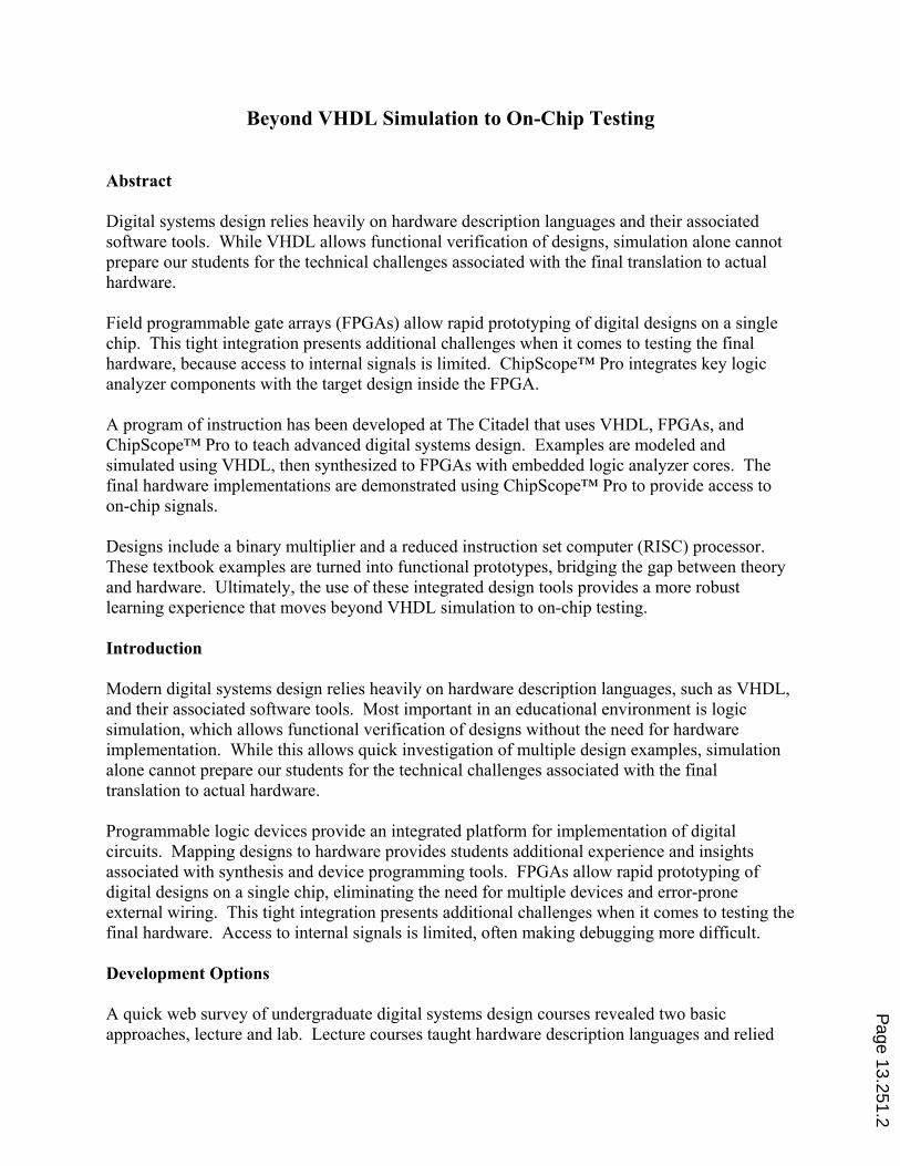
Students in our introductory digital design course are already exposed to the Xilinx® design
environment2 and implementing projects on FPGA trainers with limited I/O. As the complexity
of designs and the density of FPGA devices increase, so does the impracticality of attaching test
equipment probes to these devices under test. Xilinx now provides optional real-time
verification tools that provide on-chip debug at or near operating system speed. The
ChipScope™ Pro3 tools integrate key logic analyzer and other test and measurement hardware
components with the target design inside the FPGA. The ChipScope™ Pro tools communicate
with these components and provide the designer with a robust logic analyzer solution as shown
in Figure 1.
Figure 1. ChipScope™ Pro Test Configuration.
Page 13.251.3
Course Content
A program of instruction has been developed at The Citadel that uses VHDL, FPGAs, and
ChipScope™ Pro to teach advanced digital systems design. Throughout the course, digital
designs are first modeled using VHDL and then functionally verified via logic simulation.
Designs are then synthesized and mapped to target FPGA devices4 providing valuable insights
into the practicalities and limitations of hardware implementation. Logic analyzer and
input/output cores are embedded into the FPGA designs, providing a real-time test and
verification system. The final hardware implementations are then demonstrated using
ChipScope™ Pro to provide access to on-chip signals.
Design examples used in this course include binary, two’s complement, and floating-point
multipliers, a universal asynchronous receiver-transmitter (UART), and a RISC processor based
on the MIPS instruction set architecture. All designs are modeled and verified in VHDL, then
realized and tested on an FPGA. For the purpose of this paper a simple binary multiplier will be
used to illustrate the progression from VHDL model to FPGA hardware. Additionally some
insights are provided from the MIPS processor, demonstrating how these textbook examples are
turned into functional prototypes, bridging the gap between theory and actual hardware.
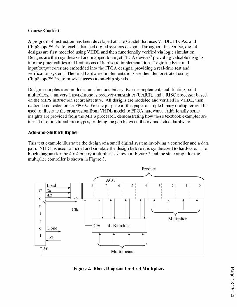
Add-and-Shift Multiplier
This text example illustrates the design of a small digital system involving a controller and a data
path. VHDL is used to model and simulate the design before it is synthesized to hardware. The
block diagram for the 4 x 4 binary multiplier is shown in Figure 2 and the state graph for the
multiplier controller is shown in Figure 3.
Figure 2. Block Diagram for 4 x 4 Multiplier.
Page 13.251.4
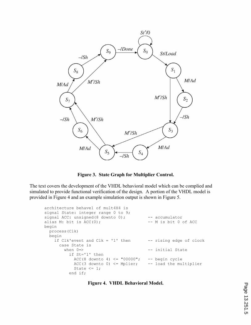
Figure 3. State Graph for Multiplier Control.
The text covers the development of the VHDL behavioral model which can be complied and
simulated to provide functional verification of the design. A portion of the VHDL model is
provided in Figure 4 and an example simulation output is shown in Figure 5.
architecture behave1 of mult4X4 is signal State: integer range 0 to 9; signal ACC: unsigned(8 downto 0); -- accumulator alias M: bit is ACC(0); -- M is bit 0 of ACC begin process(Clk) begin if Clk'event and Clk = '1' then -- rising edge of clock case State is when 0=> -- initial State if St='1' then ACC(8 downto 4) <= "00000"; -- begin cycle ACC(3 downto 0) <= Mplier; -- load the multiplier State <= 1; end if;
Figure 4. VHDL Behavioral Model.
Page 13.251.5
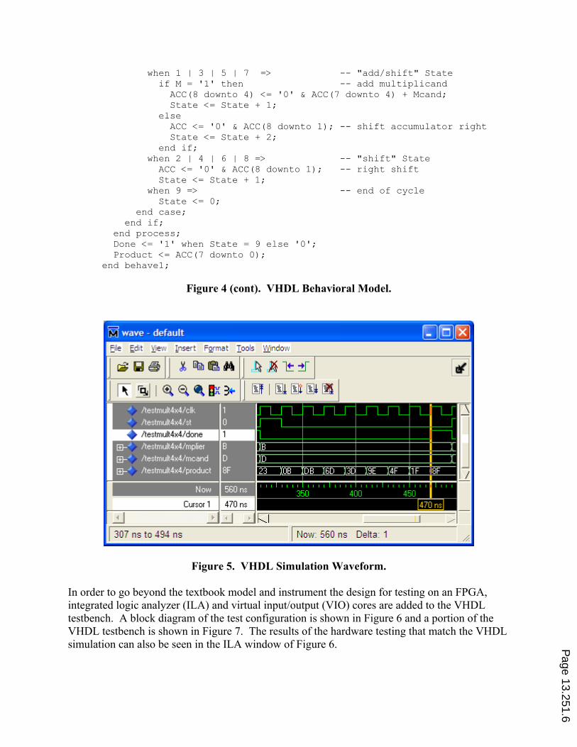
when 1 | 3 | 5 | 7 => -- "add/shift" State
<= '0' & ACC(8 downto 1); -- shift accumulator right
| 6 | 8 => -- "shift" State
-- end of cycle
;
Figure 4 (cont). VHDL Behavioral Model.
if M = '1' then -- add multiplicand ACC(8 downto 4) <= '0' & ACC(7 downto 4) + Mcand; State <= State + 1; else ACC State <= State + 2; end if; when 2 | 4 ACC <= '0' & ACC(8 downto 1); -- right shift State <= State + 1; when 9 => State <= 0; end case; end if; end process Done <= '1' when State = 9 else '0'; Product <= ACC(7 downto 0); end behave1;
Figure 5. VHDL Simulation Waveform.
order to go beyond the textbook model and instrument the design for testing on an FPGA,
L
In
integrated logic analyzer (ILA) and virtual input/output (VIO) cores are added to the VHDL
testbench. A block diagram of the test configuration is shown in Figure 6 and a portion of the
VHDL testbench is shown in Figure 7. The results of the hardware testing that match the VHD
simulation can also be seen in the ILA window of Figure 6.
Page 13.251.6
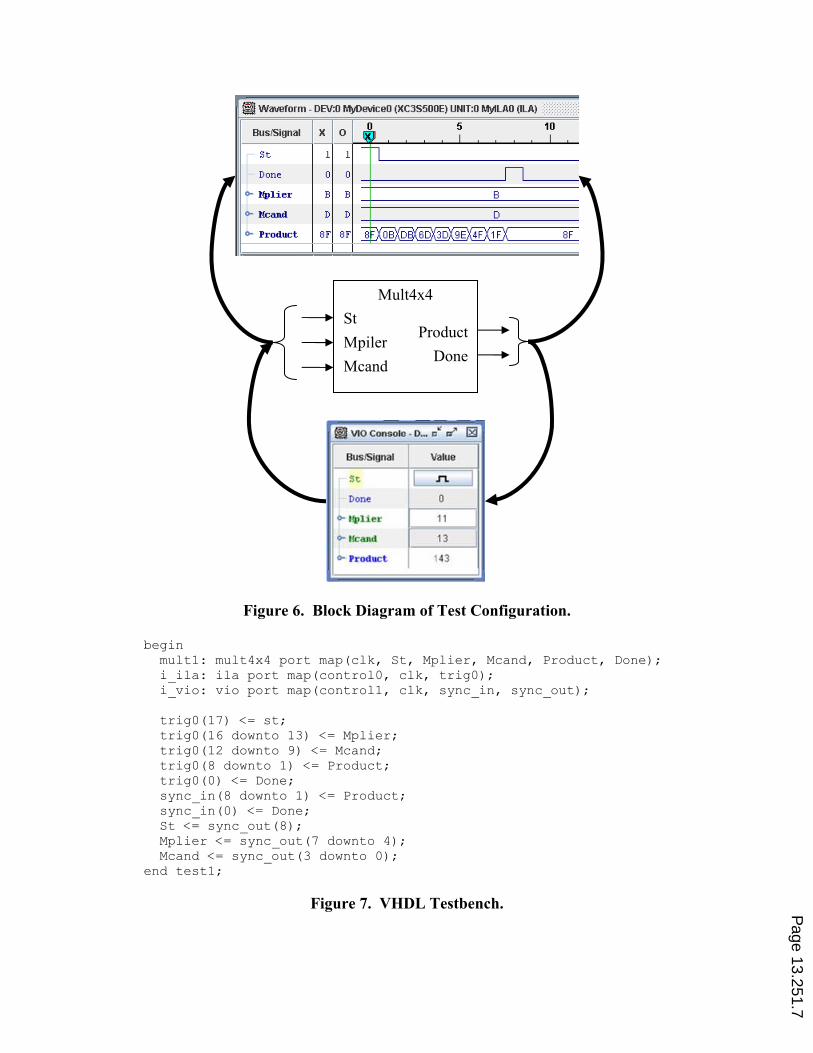
Mpiler
Mcand
St Product
Mult4x4
Done
Figure 6. Block Diagram of Test Configuration.
begin mult1: mult4x4 port map(clk, St, Mplier, Mcand, Product, Done); i_ila: ila port map(control0, clk, trig0); i_vio: vio port map(control1, clk, sync_in, sync_out); trig0(17) <= st; trig0(16 downto 13) <= Mplier; trig0(12 downto 9) <= Mcand; trig0(8 downto 1) <= Product; trig0(0) <= Done; sync_in(8 downto 1) <= Product; sync_in(0) <= Done; St <= sync_out(8); Mplier <= sync_out(7 downto 4); Mcand <= sync_out(3 downto 0); end test1;
Figure 7. VHDL Testbench.
Page 13.251.7
The VHDL model and simulation are used as a live classroom demonstration to reinforce the
textbook theory. Beyond the simulation, the actual FPGA hardware implementation is also
demonstrated in class. The VIO and ILA cores provide an interactive test environment that can
be manipulated in real-time, bridging the gap from VHDL to hardware.
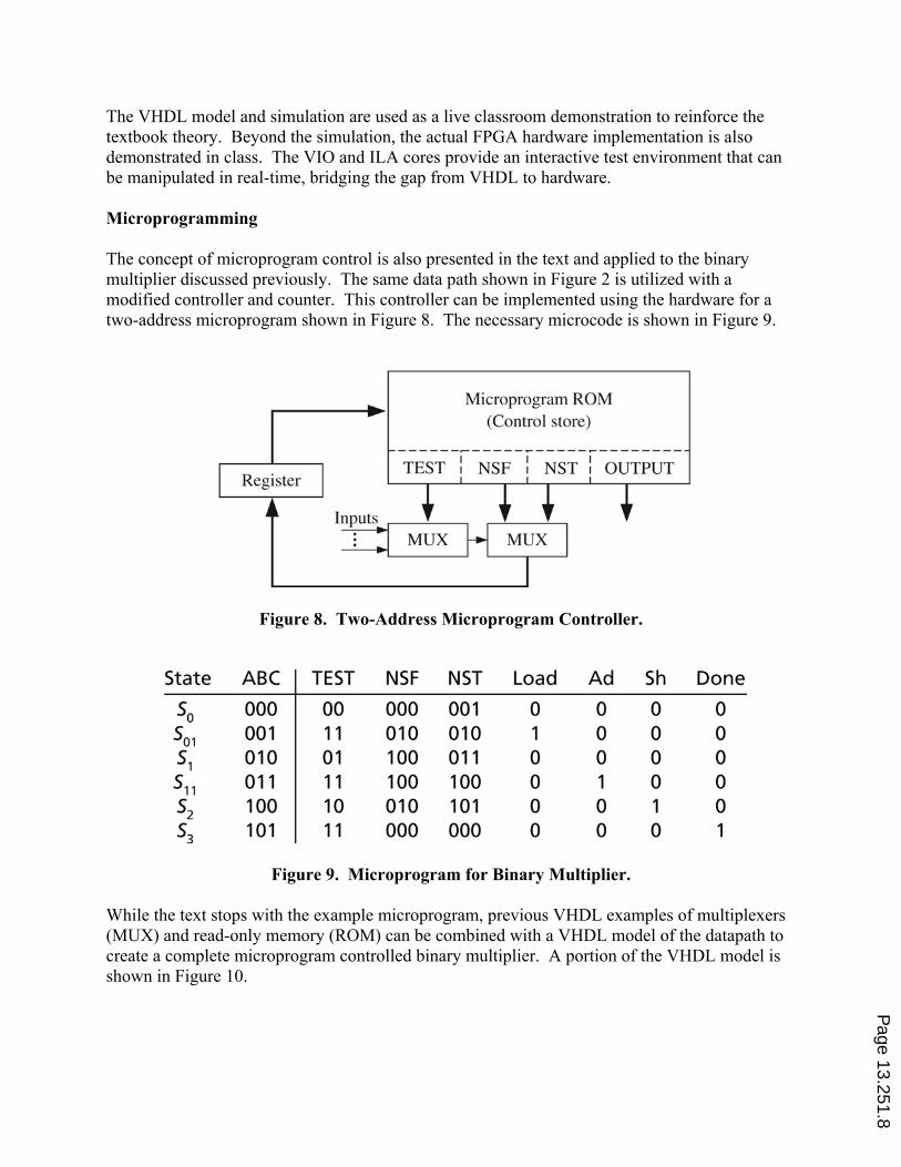
Microprogramming
The concept of microprogram control is also presented in the text and applied to the binary
multiplier discussed previously. The same data path shown in Figure 2 is utilized with a
modified controller and counter. This controller can be implemented using the hardware for a
two-address microprogram shown in Figure 8. The necessary microcode is shown in Figure 9.
Figure 8. Two-Address Microprogram Controller.
Figure 9. Microprogram for Binary Multiplier.
While the text stops with the example microprogram, previous VHDL examples of multiplexers
(MUX) and read-only memory (ROM) can be combined with a VHDL model of the datapath to
create a complete microprogram controlled binary multiplier. A portion of the VHDL model is
shown in Figure 10.
Page 13.251.8
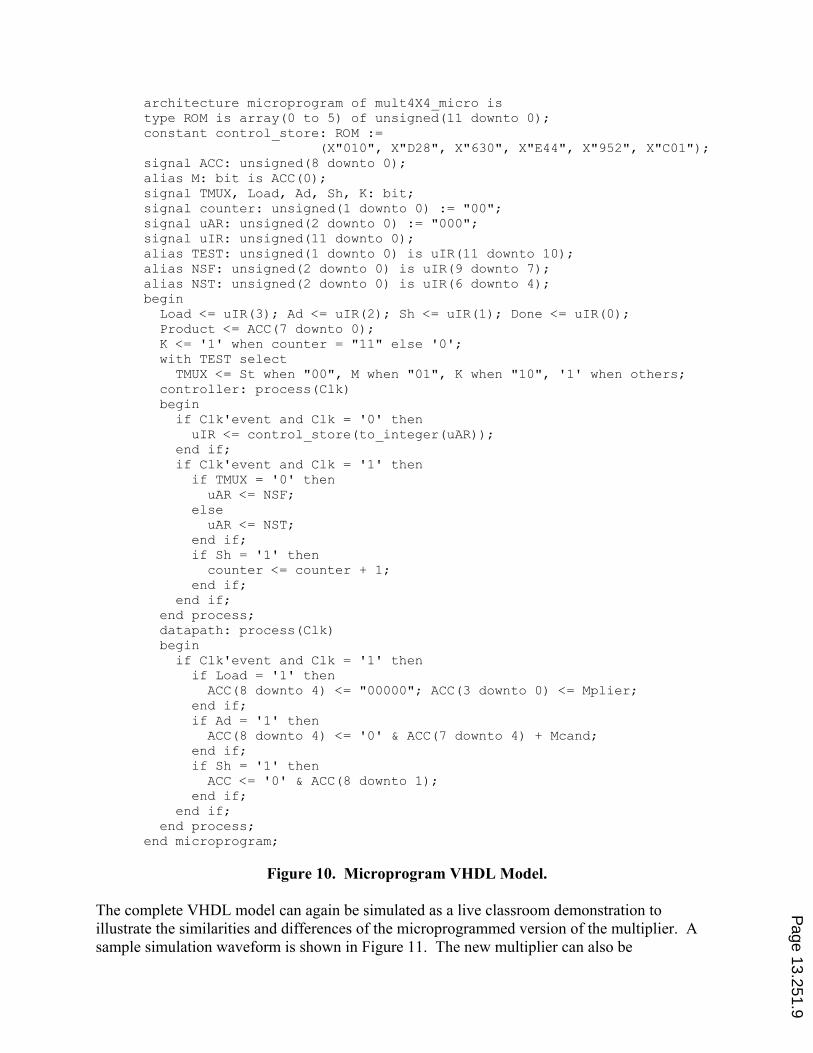
architecture microprogram of mult4X4_micro is type ROM is array(0 to 5) of unsigned(11 downto 0); constant control_store: ROM := (X"010", X"D28", X"630", X"E44", X"952", X"C01"); signal ACC: unsigned(8 downto 0); alias M: bit is ACC(0); signal TMUX, Load, Ad, Sh, K: bit; signal counter: unsigned(1 downto 0) := "00"; signal uAR: unsigned(2 downto 0) := "000"; signal uIR: unsigned(11 downto 0); alias TEST: unsigned(1 downto 0) is uIR(11 downto 10); alias NSF: unsigned(2 downto 0) is uIR(9 downto 7); alias NST: unsigned(2 downto 0) is uIR(6 downto 4); begin Load <= uIR(3); Ad <= uIR(2); Sh <= uIR(1); Done <= uIR(0); Product <= ACC(7 downto 0); K <= '1' when counter = "11" else '0'; with TEST select TMUX <= St when "00", M when "01", K when "10", '1' when others; controller: process(Clk) begin if Clk'event and Clk = '0' then uIR <= control_store(to_integer(uAR)); end if; if Clk'event and Clk = '1' then if TMUX = '0' then uAR <= NSF; else uAR <= NST; end if; if Sh = '1' then counter <= counter + 1; end if; end if; end process; datapath: process(Clk) begin if Clk'event and Clk = '1' then if Load = '1' then ACC(8 downto 4) <= "00000"; ACC(3 downto 0) <= Mplier; end if; if Ad = '1' then ACC(8 downto 4) <= '0' & ACC(7 downto 4) + Mcand; end if; if Sh = '1' then ACC <= '0' & ACC(8 downto 1); end if; end if; end process; end microprogram;
Figure 10. Microprogram VHDL Model.
The complete VHDL model can again be simulated as a live classroom demonstration to
illustrate the similarities and differences of the microprogrammed version of the multiplier. A
sample simulation waveform is shown in Figure 11. The new multiplier can also be
Page 13.251.9
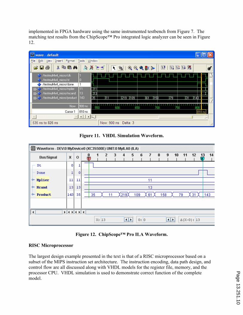
implemented in FPGA hardware using the same instrumented testbench from Figure 7. The
matching test results from the ChipScope™ Pro integrated logic analyzer can be seen in Figure
12.
Figure 11. VHDL Simulation Waveform.
Figure 12. ChipScope™ Pro ILA Waveform.
RISC Microprocessor
The largest design example presented in the text is that of a RISC microprocessor based on a
subset of the MIPS instruction set architecture. The instruction encoding, data path design, and
control flow are all discussed along with VHDL models for the register file, memory, and the
processor CPU. VHDL simulation is used to demonstrate correct function of the complete
model.
Page 13.251.10
To facilitate synthesis of the VHDL model to a functional FPGA implementation, several minor
modifications were necessary. First, the text model for the register file needed to be modified for
synchronous read and write in order to correctly synthesize to Block RAM on the FPGA.
Though the text model would simulate correctly, the resulting hardware would fail under testing.
This exception is used as an important design lesson pointing out valuable insights into actual
hardware realization.
The second modification was to alter the text memory model to allow initialization separate from
the testbench. The new memory model uses a VHDL type with initial values, which allows the
contents to be set at compile time. Machine code can now be loaded directly into memory,
greatly simplifying the overarching testbench. A sample MIPS program is shown loaded into
memory in Figure 13.
architecture Internal of Memory is type RAMtype is array (0 to 127) of unsigned(31 downto 0); signal RAM1: RAMtype := ( x"30630000", -- andi $3, $3, 0 x"30420000", -- andi $2, $2, 0 x"20420005", -- addi $2, $2, 5 x"8C650040", -- lw $5, 64($3) x"8C660048", -- lw $6, 72($3) x"00A63820", -- add $7, $5, $6 x"AC670050", -- sw $7, 80($3) x"20630001", -- addi $3, $3, 1 x"1462FFFA", -- bne $3, $2, -6 x"08000009", -- j 9
Figure 13. Memory Initialization.
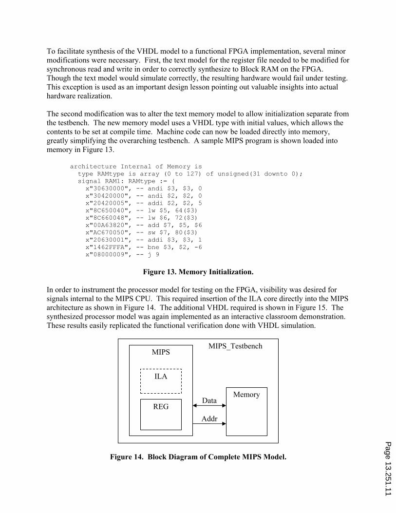
In order to instrument the processor model for testing on the FPGA, visibility was desired for
signals internal to the MIPS CPU. This required insertion of the ILA core directly into the MIPS
architecture as shown in Figure 14. The additional VHDL required is shown in Figure 15. The
synthesized processor model was again implemented as an interactive classroom demonstration.
These results easily replicated the functional verification done with VHDL simulation.
Memory
REG
ILA
MIPS
Data
Addr
MIPS_Testbench
Figure 14. Block Diagram of Complete MIPS Model.
Page 13.251.11
i_ila: ila port map(control0, clk, trig0); trig0(178) <= RST; trig0(177) <= CS; trig0(176) <= WE; trig0(175 downto 144) <= Addr; trig0(143 downto 112) <= Mem_Bus; trig0(111) <= RegW; trig0(110 downto 106) <= SR1; trig0(105 downto 101) <= SR2; trig0(100 downto 96) <= DR; trig0(95 downto 64) <= Reg_In; trig0(63 downto 32) <= ReadReg1; trig0(31 downto 0) <= ReadReg2;
Figure 15. VHDL for ILA Core.
This example shows the true power of the ChipScope™ Pro tools. With only a minor
modification to the VHDL model, internal signals totaling 179 bits of information can be
captured and traced with the integrated logic analyzer. Using conventional methods, these
signals would need to be converted to ports and routed to I/O pins before being connected to an
external logic analyzer. This extra routing and loading is cumbersome and could greatly alter the
timing and performance of the hardware under test.
Results and Conclusions
The program of instruction described in this paper will be implemented at The Citadel in a pilot
lecture course during the spring semester 2008. The approach is to supplement textbook
examples with interactive classroom demonstrations involving both VHDL simulation and on-
chip testing of FPGA hardware implementations. Planned enrollment is 15 seniors in two
sections, which should provide the desired level of interaction and feedback.
Current plans are to keep student homework assignments limited to VHDL simulations.
ModelSim® PE Student Edition5 is included with the course text and provides the students a
simulation environment available on their own PC or in the department computer labs. Partially
due to cost considerations, licensing for the ChipScope™ Pro tools is currently limited to one
faculty and one classroom computer.
Based on the success of the program of instruction and student feedback, future directions may
include adding FPGA projects to student homework assignments. FPGA trainers are readily
available from the introductory digital design course which is taught in the fall. The value added
of hardware assignments will need to be weighed against software license costs, restricted
availability of such software, and increased demands on student time. Classroom demonstrations
may or may not prove sufficient to convey the desired concepts.
In summary what was desired was a lecture course in advanced digital systems design that also
emphasized hardware, but without the time and expense of a lab. Design examples are modeled
and verified in VHDL, then realized and tested on an FPGA. Thus, these textbook examples are
turned into functional prototypes, bridging the gap between theory and actual hardware.
Page 13.251.12
Ultimately, the use of these integrated design tools provides a more robust learning experience
that moves beyond VHDL simulation to hardware implementation and on-chip testing.
Acknowledgments
This project was enabled by the generous funding of The Citadel Foundation. Many thanks for
their continued support of numerous programs that support this institution.
Bibliography
1. Roth, C. and L. John, Digital Systems Design Using VHDL, Second Edition, Thompson, Toronto, Canada, 2008.
2. Xilinx ISE 9.1i Software Manuals, Xilinx, Inc., 2007.
3. ChipScope™ Pro Software and Cores User Guide, Xilinx, Inc., 2007.
4. Spartan-3E Starter Kit Board User Guide, Xilinx, Inc., 2006.
5. ModelSim PE Student Edition, Mentor Graphics Corp., 2007.
Page 13.251.13


![VHDL Simulation Tutorials [INFN Torino Wiki]](https://img.pdfslide.net/doc/110x75/577cc84d1a28aba711a27005/vhdl-simulation-tutorials-infn-torino-wiki.jpg)