Embed Size (px)
Citation preview
RF and Protect ion Devices
BGS16MN14
Appl icat ion Note AN368 Revision: Rev. 1.0
2014-05-23
SP6T Antenna Switch
Diversi ty RF Frontend Appl icat ions

Edition 2014-06-02
Published by Infineon Technologies AG 81726 Munich, Germany
© 2014 Infineon Technologies AG All Rights Reserved.
LEGAL DISCLAIMER
THE INFORMATION GIVEN IN THIS APPLICATION NOTE IS GIVEN AS A HINT FOR THE IMPLEMENTATION OF THE INFINEON TECHNOLOGIES COMPONENT ONLY AND SHALL NOT BE REGARDED AS ANY DESCRIPTION OR WARRANTY OF A CERTAIN FUNCTIONALITY, CONDITION OR QUALITY OF THE INFINEON TECHNOLOGIES COMPONENT. THE RECIPIENT OF THIS APPLICATION NOTE MUST VERIFY ANY FUNCTION DESCRIBED HEREIN IN THE REAL APPLICATION. INFINEON TECHNOLOGIES HEREBY DISCLAIMS ANY AND ALL WARRANTIES AND LIABILITIES OF ANY KIND (INCLUDING WITHOUT LIMITATION WARRANTIES OF NON-INFRINGEMENT OF INTELLECTUAL PROPERTY RIGHTS OF ANY THIRD PARTY) WITH RESPECT TO ANY AND ALL INFORMATION GIVEN IN THIS APPLICATION NOTE.
Information
For further information on technology, delivery terms and conditions and prices, please contact the nearest Infineon Technologies Office (www.infineon.com).
Warnings
Due to technical requirements, components may contain dangerous substances. For information on the types in question, please contact the nearest Infineon Technologies Office.
Infineon Technologies components may be used in life-support devices or systems only with the express written approval of Infineon Technologies, if a failure of such components can reasonably be expected to cause the failure of that life-support device or system or to affect the safety or effectiveness of that device or system. Life support devices or systems are intended to be implanted in the human body or to support and/or maintain and sustain and/or protect human life. If they fail, it is reasonable to assume that the health of the user or other persons may be endangered.
BGS16MN14 Diversity RF Frontend Applications
Application Note AN368, Rev. 1.0 2014-05-23 3 / 20
Application Note AN368
Revision History: 2014-05-23
Previous Revision: prev. Rev. x.x
Page Subjects (major changes since last revision)
Trademarks of Infineon Technologies AG
AURIX™, C166™, CanPAK™, CIPOS™, CIPURSE™, EconoPACK™, CoolMOS™, CoolSET™, CORECONTROL™, CROSSAVE™, DAVE™, DI-POL™, EasyPIM™, EconoBRIDGE™, EconoDUAL™, EconoPIM™, EconoPACK™, EiceDRIVER™, eupec™, FCOS™, HITFET™, HybridPACK™, I²RF™, ISOFACE™, IsoPACK™, MIPAQ™, ModSTACK™, my-d™, NovalithIC™, OptiMOS™, ORIGA™, POWERCODE™, PRIMARION™, PrimePACK™, PrimeSTACK™, PRO-SIL™, PROFET™, RASIC™, ReverSave™, SatRIC™, SIEGET™, SINDRION™, SIPMOS™, SmartLEWIS™, SOLID FLASH™, TEMPFET™, thinQ!™, TRENCHSTOP™, TriCore™.
Other Trademarks
Advance Design System™ (ADS) of Agilent Technologies, AMBA™, ARM™, MULTI-ICE™, KEIL™, PRIMECELL™, REALVIEW™, THUMB™, µVision™ of ARM Limited, UK. AUTOSAR™ is licensed by AUTOSAR development partnership. Bluetooth™ of Bluetooth SIG Inc. CAT-iq™ of DECT Forum. COLOSSUS™, FirstGPS™ of Trimble Navigation Ltd. EMV™ of EMVCo, LLC (Visa Holdings Inc.). EPCOS™ of Epcos AG. FLEXGO™ of Microsoft Corporation. FlexRay™ is licensed by FlexRay Consortium. HYPERTERMINAL™ of Hilgraeve Incorporated. IEC™ of Commission Electrotechnique Internationale. IrDA™ of Infrared Data Association Corporation. ISO™ of INTERNATIONAL ORGANIZATION FOR STANDARDIZATION. MATLAB™ of MathWorks, Inc. MAXIM™ of Maxim Integrated Products, Inc. MICROTEC™, NUCLEUS™ of Mentor Graphics Corporation. MIPI™ of MIPI Alliance, Inc. MIPS™ of MIPS Technologies, Inc., USA. muRata™ of MURATA MANUFACTURING CO., MICROWAVE OFFICE™ (MWO) of Applied Wave Research Inc., OmniVision™ of OmniVision Technologies, Inc. Openwave™ Openwave Systems Inc. RED HAT™ Red Hat, Inc. RFMD™ RF Micro Devices, Inc. SIRIUS™ of Sirius Satellite Radio Inc. SOLARIS™ of Sun Microsystems, Inc. SPANSION™ of Spansion LLC Ltd. Symbian™ of Symbian Software Limited. TAIYO YUDEN™ of Taiyo Yuden Co. TEAKLITE™ of CEVA, Inc. TEKTRONIX™ of Tektronix Inc. TOKO™ of TOKO KABUSHIKI KAISHA TA. UNIX™ of X/Open Company Limited. VERILOG™, PALLADIUM™ of Cadence Design Systems, Inc. VLYNQ™ of Texas Instruments Incorporated. VXWORKS™, WIND RIVER™ of WIND RIVER SYSTEMS, INC. ZETEX™ of Diodes Zetex Limited.
Last Trademarks Update 2011-11-11
BGS16MN14 Diversity RF Frontend Applications
List of Content, Figures and Tables
Application Note AN368, Rev. 1.0 2014-05-23 4 / 20
Table of Content
1 Introduction ........................................................................................................................................ 6
2 BGS16MN14 Features ........................................................................................................................ 6 2.1 Main Features ...................................................................................................................................... 6 2.2 Functional Diagram .............................................................................................................................. 6 2.3 Pin Configuration .................................................................................................................................. 7 2.4 Pin Description ..................................................................................................................................... 7
3 Application .......................................................................................................................................... 8 3.1 Application Board ................................................................................................................................. 8
4 Small Signal Characteristics ........................................................................................................... 10 4.1 Insertion Loss from Antenna to the respective RF port...................................................................... 10 4.2 Return Loss from Antenna to the respective RF port ......................................................................... 10 4.3 Forward Transmission ........................................................................................................................ 11 4.4 Reflection Antenna Port ..................................................................................................................... 11 4.5 Port Reflection .................................................................................................................................... 12 4.6 Antenna Isolation Neighbour Ports .................................................................................................... 12 4.7 Port Isolation Neighbour Ports ........................................................................................................... 13
5 Intermodulation ................................................................................................................................ 14 5.1 Introduction ......................................................................................................................................... 14 5.2 IMD Test Set-up ................................................................................................................................. 14 5.3 IMD Test Results for Band 1 and 5 .................................................................................................... 15
6 Harmonic Generation ....................................................................................................................... 15
7 Appendix: Switch Controller Unit ................................................................................................... 18 7.1 Operating Guide ................................................................................................................................. 18
8 Authors .............................................................................................................................................. 19
BGS16MN14 Diversity RF Frontend Applications
List of Content, Figures and Tables
Application Note AN368, Rev. 1.0 2014-05-23 5 / 20
List of Figures
Figure 1 BGS16MN14 Functional Diagram ....................................................................................................... 6 Figure 2 BGS16MN14 Pin Configuration ........................................................................................................... 7 Figure 3 RF switch in mobile phone cellular frontend ........................................................................................ 8 Figure 4 Layout of the application board ............................................................................................................ 9 Figure 5 Layout of de-embedding boards .......................................................................................................... 9 Figure 6 PCB layer information .......................................................................................................................... 9 Figure 7 Application circuit ............................................................................................................................... 10 Figure 8 Forward Transmission Curves for RF Ports ....................................................................................... 11 Figure 9 Reflection Antenna Port ..................................................................................................................... 11 Figure 10 Port Reflection .................................................................................................................................... 12 Figure 11 Antenna Isolation Neighbour Ports .................................................................................................... 12 Figure 12 Port Isolation of Neighbour Ports ....................................................................................................... 13 Figure 13 Block diagram of RF Switch intermodulation ..................................................................................... 14 Figure 14 Test set-up for IMD Measurements .................................................................................................... 14 Figure 15 Set-up for harmonics measurement ................................................................................................... 15 Figure 16 2
nd Harmonic at fc=824 MHz............................................................................................................... 16
Figure 17 3rd
harmonic at fc=824 MHz ................................................................................................................ 16 Figure 18 2
nd Harmonic at fc=1800 MHz............................................................................................................. 17
Figure 19 3rd
Harmonic at fc=1800 MHz ............................................................................................................. 17 Figure 20 Switch Controller Unit Board .............................................................................................................. 18
List of Tables
Table 1 Pin Description (top view) .................................................................................................................... 7 Table 2 Insertion Loss from Antenna to the respective RF port with all other ports terminated with 50Ω ...... 10 Table 3 Antenna Return Loss with all other ports terminated with 50Ω .......................................................... 10 Table 4 IMD Measurements ............................................................................................................................ 15
BGS16MN14 Diversity RF Frontend Applications
Introduction
Application Note AN368, Rev. 1.0 2014-05-23 6 / 20
1 Introduction
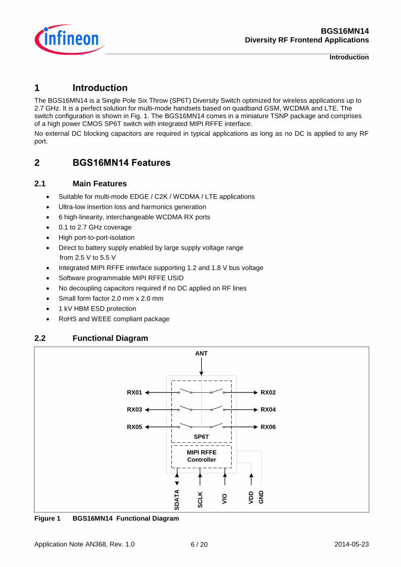
The BGS16MN14 is a Single Pole Six Throw (SP6T) Diversity Switch optimized for wireless applications up to 2.7 GHz. It is a perfect solution for multi-mode handsets based on quadband GSM, WCDMA and LTE. The switch configuration is shown in Fig. 1. The BGS16MN14 comes in a miniature TSNP package and comprises of a high power CMOS SP6T switch with integrated MIPI RFFE interface.
No external DC blocking capacitors are required in typical applications as long as no DC is applied to any RF port.
2 BGS16MN14 Features
2.1 Main Features
Suitable for multi-mode EDGE / C2K / WCDMA / LTE applications
Ultra-low insertion loss and harmonics generation
6 high-linearity, interchangeable WCDMA RX ports
0.1 to 2.7 GHz coverage
High port-to-port-isolation
Direct to battery supply enabled by large supply voltage range
from 2.5 V to 5.5 V
Integrated MIPI RFFE interface supporting 1.2 and 1.8 V bus voltage
Software programmable MIPI RFFE USID
No decoupling capacitors required if no DC applied on RF lines
Small form factor 2.0 mm x 2.0 mm
1 kV HBM ESD protection
RoHS and WEEE compliant package
2.2 Functional Diagram
Figure 1 BGS16MN14 Functional Diagram
MIPI RFFE
Controller
SD
AT
A
SC
LK
VD
D
GN
D
VIO
ANT
RX01 RX02
RX03 RX04
RX05
SP6T
RX06
BGS16MN14 Diversity RF Frontend Applications
BGS16MN14 Features
Application Note AN368, Rev. 1.0 2014-05-23 7 / 20
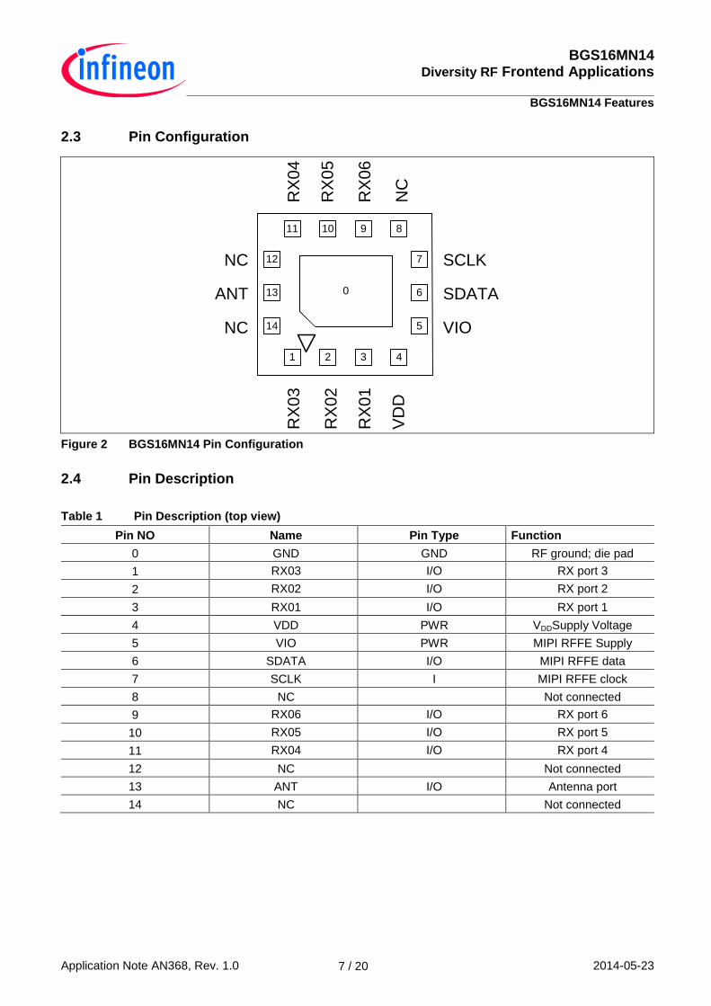
2.3 Pin Configuration
Figure 2 BGS16MN14 Pin Configuration
2.4 Pin Description
Table 1 Pin Description (top view)
Pin NO Name Pin Type Function
0 GND GND RF ground; die pad
1 RX03 I/O RX port 3
2 RX02 I/O RX port 2
3 RX01 I/O RX port 1
4 VDD PWR VDDSupply Voltage
5 VIO PWR MIPI RFFE Supply
6 SDATA I/O MIPI RFFE data
7 SCLK I MIPI RFFE clock
8 NC Not connected
9 RX06 I/O RX port 6
10 RX05 I/O RX port 5
11 RX04 I/O RX port 4
12 NC Not connected
13 ANT I/O Antenna port
14 NC Not connected
91011
SCLK
VIO
SDATAR
X0
4
12
13
8
14
7
6
5
4321
NC
NC
VD
DN
C
ANT
RX
05
RX
01
RX
02
RX
03
RX
06
0
BGS16MN14 Diversity RF Frontend Applications
Application
Application Note AN368, Rev. 1.0 2014-05-23 8 / 20
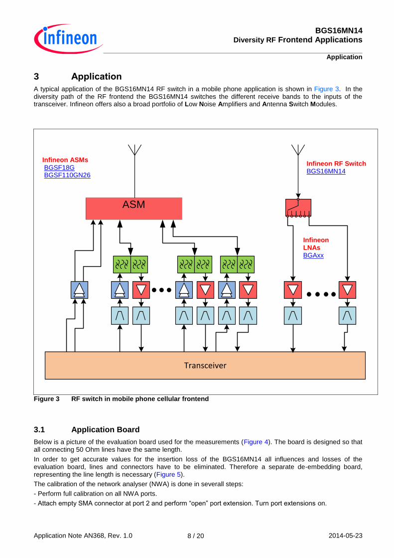
3 Application
A typical application of the BGS16MN14 RF switch in a mobile phone application is shown in Figure 3. In the diversity path of the RF frontend the BGS16MN14 switches the different receive bands to the inputs of the transceiver. Infineon offers also a broad portfolio of Low Noise Amplifiers and Antenna Switch Modules.
Figure 3 RF switch in mobile phone cellular frontend
3.1 Application Board
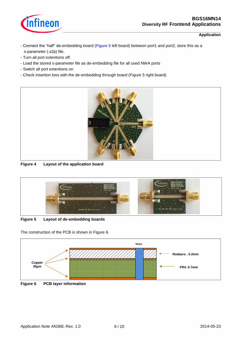
Below is a picture of the evaluation board used for the measurements (Figure 4). The board is designed so that all connecting 50 Ohm lines have the same length.
In order to get accurate values for the insertion loss of the BGS16MN14 all influences and losses of the evaluation board, lines and connectors have to be eliminated. Therefore a separate de-embedding board, representing the line length is necessary (Figure 5).
The calibration of the network analyser (NWA) is done in severall steps:
- Perform full calibration on all NWA ports.
- Attach empty SMA connector at port 2 and perform “open” port extension. Turn port extensions on.
Transceiver
ASM
Infineon ASMs BGSF18G BGSF110GN26
Infineon RF Switch BGS16MN14
Infineon LNAs BGAxx
BGS16MN14 Diversity RF Frontend Applications
Application
Application Note AN368, Rev. 1.0 2014-05-23 9 / 20
- Connect the “half” de-embedding board (Figure 5 left board) between port1 and port2, store this as a
s-parameter (.s2p) file.
- Turn all port extentions off.
- Load the stored s-parameter file as de-embedding file for all used NWA ports
- Switch all port extentions on
- Check insertion loss with the de-embedding through board (Figure 5 right board)
Figure 4 Layout of the application board
Figure 5 Layout of de-embedding boards
The construction of the PCB is shown in Figure 6.
Figure 6 PCB layer information
Copper
35µm
Rodgers , 0.2mm
FR4, 0.7mm
Vias
BGS16MN14 Diversity RF Frontend Applications
Small Signal Characteristics
Application Note AN368, Rev. 1.0 2014-05-23 10 / 20
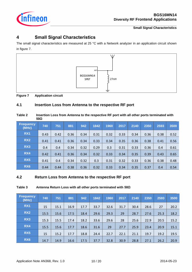
4 Small Signal Characteristics
The small signal characteristics are measured at 25 °C with a Network analyzer in an application circuit shown
in figure 7.
Figure 7 Application circuit
4.1 Insertion Loss from Antenna to the respective RF port
Table 2 Insertion Loss from Antenna to the respective RF port with all other ports terminated with 50Ω
Frequency (MHz)
740 751 881 942 1842 1960 2017 2140 2350 2593 3500
RX1 0.43 0.42 0.36 0.34 0.31 0.32 0.33 0.34 0.36 0.38 0.52
RX2 0.41 0.41 0.36 0.34 0.33 0.34 0.35 0.36 0.38 0.41 0.56
RX3 0.4 0.4 0.34 0.32 0.29 0.3 0.31 0.33 0.36 0.4 0.61
RX4 0.42 0.41 0.36 0.34 0.32 0.33 0.34 0.35 0.39 0.43 0.65
RX5 0.41 0.4 0.34 0.32 0.3 0.31 0.32 0.33 0.36 0.38 0.48
RX6 0.44 0.44 0.38 0.36 0.32 0.33 0.34 0.35 0.37 0.4 0.54
4.2 Return Loss from Antenna to the respective RF port
Table 3 Antenna Return Loss with all other ports terminated with 50Ω
Frequency (MHz)
740 751 881 942 1842 1960 2017 2140 2350 2593 3500
RX1 15 15.1 16.9 17.7 33.7 32.6 31.7 30.4 28.6 27 20.2
RX2 15.5 15.6 17.5 18.4 29.6 29.3 29 28.7 27.6 25.3 18.2
RX3 15.3 15.5 17.4 18.2 33.6 29.6 28 25.6 22.9 20.5 15.2
RX4 15.5 15.6 17.7 18.6 31.6 29 27.7 25.9 23.4 20.9 15.1
RX5 15 15.2 17.7 18.8 24.4 22.7 22.1 21.1 19.7 19.2 19.5
RX6 14.7 14.9 16.6 17.5 37.7 32.8 30.9 28.8 27.1 26.2 20.9
27nH
ANT
BGS16MN14SP6T
BGS16MN14 Diversity RF Frontend Applications
Small Signal Characteristics
Application Note AN368, Rev. 1.0 2014-05-23 11 / 20
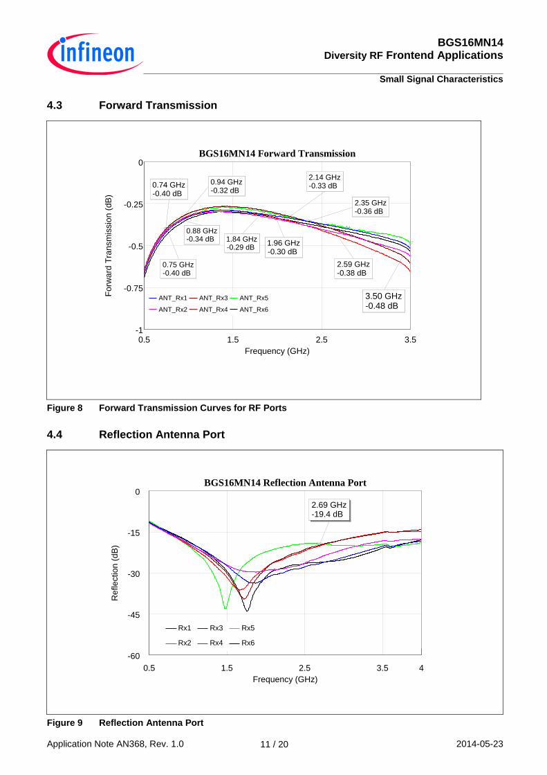
4.3 Forward Transmission
Figure 8 Forward Transmission Curves for RF Ports
4.4 Reflection Antenna Port
Figure 9 Reflection Antenna Port
0.5 1.5 2.5 3.5
Frequency (GHz)
BGS16MN14 Forward Transmission
-1
-0.75
-0.5
-0.25
0
Forw
ard
Tra
nsm
issio
n (
dB
)
2.59 GHz-0.38 dB
2.35 GHz-0.36 dB
3.50 GHz-0.48 dB
1.96 GHz-0.30 dB
2.14 GHz-0.33 dB
1.84 GHz-0.29 dB
0.94 GHz-0.32 dB
0.88 GHz-0.34 dB
0.75 GHz-0.40 dB
0.74 GHz-0.40 dB
ANT_Rx1
ANT_Rx2
ANT_Rx3
ANT_Rx4
ANT_Rx5
ANT_Rx6
0.5 1.5 2.5 3.5 4
Frequency (GHz)
BGS16MN14 Reflection Antenna Port
-60
-45
-30
-15
0
Reflection (
dB
)
2.69 GHz-19.4 dB
Rx1
Rx2
Rx3
Rx4
Rx5
Rx6
BGS16MN14 Diversity RF Frontend Applications
Small Signal Characteristics
Application Note AN368, Rev. 1.0 2014-05-23 12 / 20
4.5 Port Reflection
Figure 10 Port Reflection
4.6 Antenna Isolation Neighbour Ports
Figure 11 Antenna Isolation Neighbour Ports
0.5 1.5 2.5 3.5 4
Frequency (GHz)
BGS16MN14 Reflection Rx Ports
-70
-55
-40
-25
-10
0
Reflection (
dB
)
2.69 GHz-16.95 dB
Rx1
Rx2
Rx3
Rx4
Rx5
Rx6
0.05 1.05 2.05 3.05 3.5
Frequency (GHz)
Antenna Isolation of Neighbour Ports
-100
-80
-60
-40
-20
0
Isola
tion (
dB
)
2.69 GHz-27.86 dB
Rx1 activeANT_Rx2
Rx1 activeANT_Rx6
Rx2 activeANT_Rx3
Rx2 activeANT_Rx1
Rx3 activeANT_Rx4
Rx3 activeANT_Rx2
Rx4 activeANT_Rx5
Rx4 activeANT_Rx3
Rx5 activeANT_Rx6
Rx5 activeANT_Rx4
Rx6 activeANT_Rx1
Rx6 activeANT_Rx5
BGS16MN14 Diversity RF Frontend Applications
Small Signal Characteristics
Application Note AN368, Rev. 1.0 2014-05-23 13 / 20
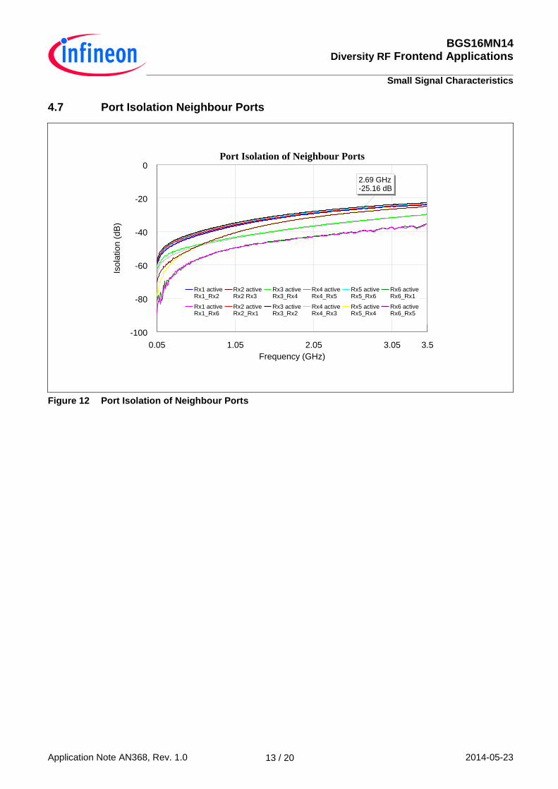
4.7 Port Isolation Neighbour Ports
Figure 12 Port Isolation of Neighbour Ports
0.05 1.05 2.05 3.05 3.5
Frequency (GHz)
Port Isolation of Neighbour Ports
-100
-80
-60
-40
-20
0
Isola
tion (
dB
)
2.69 GHz-25.16 dB
Rx1 activeRx1_Rx2
Rx1 activeRx1_Rx6
Rx2 activeRx2 Rx3
Rx2 activeRx2_Rx1
Rx3 activeRx3_Rx4
Rx3 activeRx3_Rx2
Rx4 activeRx4_Rx5
Rx4 activeRx4_Rx3
Rx5 activeRx5_Rx6
Rx5 activeRx5_Rx4
Rx6 activeRx6_Rx1
Rx6 activeRx6_Rx5
BGS16MN14 Diversity RF Frontend Applications
Intermodulation
Application Note AN368, Rev. 1.0 2014-05-23 14 / 20
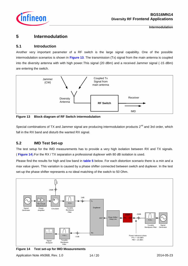
5 Intermodulation
5.1 Introduction
Another very important parameter of a RF switch is the large signal capability. One of the possible
intermodulation scenarios is shown in Figure 13. The transmission (Tx) signal from the main antenna is coupled
into the diversity antenna with with high power.This signal (20 dBm) and a received Jammer signal (-15 dBm)
are entering the switch.
Figure 13 Block diagram of RF Switch intermodulation
Special combinations of TX and Jammer signal are producing intermodulation products 2nd
and 3rd order, which
fall in the RX band and disturb the wanted RX signal.
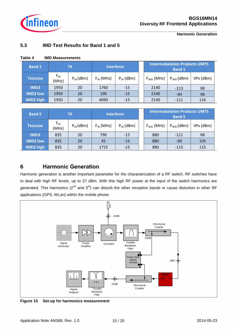
5.2 IMD Test Set-up
The test setup for the IMD measurements has to provide a very high isolation between RX and TX signals.
( Figure 14).For the RX / TX separation a professional duplexer with 80 dB isolation is used.
Please find the results for high and low band in table 5 below. For each distortion scenario there is a min and a
max value given. This variation is caused by a phase shifter connected between switch and duplexer. In the test
set-up the phase shifter represents a no ideal matching of the switch to 50 Ohm.
Figure 14 Test set-up for IMD Measurements
RF Switch
Diversity
Antenna
Receiver
Coupled Tx
Signal from
main antenna
Jammer
(CW)
IMD
Mini Circuits
(ZHL-30W-252 -S+)
Load
Signal Generator
Power Amplifier
Circulator
-20dB
Signal Analyzer
-3 dB
-3dB
Duplexer
Tx
Rx
ANTPhase Shifter /
Delay Line
Signal Generator
DUT -20dB
Tunable Bandpass Filter
K & L
Power reference planePTx = +20 dBm
PBl = -15 dBm
TRx ANT
K & L
Tunable Bandpass
Filter
K & L
Tunable
Bandpass Filter
BGS16MN14 Diversity RF Frontend Applications
Harmonic Generation
Application Note AN368, Rev. 1.0 2014-05-23 15 / 20
5.3 IMD Test Results for Band 1 and 5
Table 4 IMD Measurements
Band 1 TX Interferer
Intermodulation Products UMTS Band 1
Testcase FIN
(MHz) PIN (dBm) FIN (MHz) PIN (dBm) FIMD (MHz) PIMD (dBm) IIPx (dBm)
IMD3 1950 20 1760 -15 2140 -113 68
IMD2 low 1950 20 190 -15 2140 -94 99
IMD2 high 1950 20 4090 -15 2140 -111 116
Band 5 TX Interferer
Intermodulation Products UMTS Band 5
Testcase FIN
(MHz) PIN (dBm) FIN (MHz) PIN (dBm) FIMD (MHz) PIMD (dBm) IIPx (dBm)
IMD3 835 20 790 -15 880 -111 68
IMD2 low 835 20 45 -15 880 -99 105
IMD2 high 835 20 1715 -15 880 -110 115
6 Harmonic Generation
Harmonic generation is another important parameter for the characterization of a RF switch. RF switches have
to deal with high RF levels, up to 27 dBm. With this high RF power at the input of the switch harmonics are
generated. This harmonics (2nd
and 3rd
) can disturb the other reception bands or cause distortion in other RF
applications (GPS, WLan) within the mobile phone.
Figure 15 Set-up for harmonics measurement
Lo
ad
Signal
Generator
Power
AmplifierCirculator
Tunable
Bandpass
Filter
-20dB
Directional
Coupler
Directional
CouplerTunable
Bandstop
Filter
Signal
Analyzer
-3dB
K & L
Power meter
Agilent
E4419B
A
B
-20dB
-20dB
DUTTxANT
BGS16MN14 Diversity RF Frontend Applications
Harmonic Generation
Application Note AN368, Rev. 1.0 2014-05-23 16 / 20
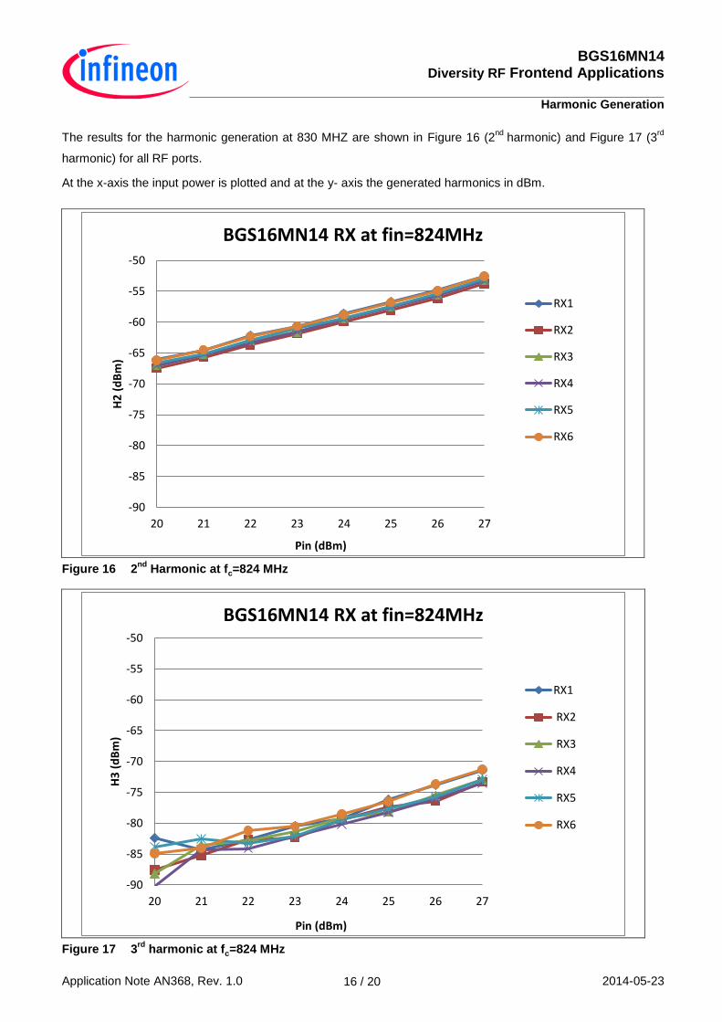
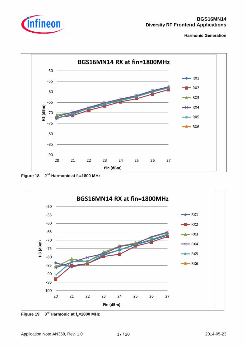
The results for the harmonic generation at 830 MHZ are shown in Figure 16 (2nd
harmonic) and Figure 17 (3rd
harmonic) for all RF ports.
At the x-axis the input power is plotted and at the y- axis the generated harmonics in dBm.
Figure 16 2nd
Harmonic at fc=824 MHz
Figure 17 3rd
harmonic at fc=824 MHz
-90
-85
-80
-75
-70
-65
-60
-55
-50
20 21 22 23 24 25 26 27
H2
(d
Bm
)
Pin (dBm)
BGS16MN14 RX at fin=824MHz
RX1
RX2
RX3
RX4
RX5
RX6
-90
-85
-80
-75
-70
-65
-60
-55
-50
20 21 22 23 24 25 26 27
H3
(d
Bm
)
Pin (dBm)
BGS16MN14 RX at fin=824MHz
RX1
RX2
RX3
RX4
RX5
RX6
BGS16MN14 Diversity RF Frontend Applications
Harmonic Generation
Application Note AN368, Rev. 1.0 2014-05-23 17 / 20
Figure 18 2nd
Harmonic at fc=1800 MHz
Figure 19 3rd
Harmonic at fc=1800 MHz
-90
-85
-80
-75
-70
-65
-60
-55
-50
20 21 22 23 24 25 26 27
H2
(d
Bm
)
Pin (dBm)
BGS16MN14 RX at fin=1800MHz
RX1
RX2
RX3
RX4
RX5
RX6
-100
-95
-90
-85
-80
-75
-70
-65
-60
-55
-50
20 21 22 23 24 25 26 27
H3
(d
Bm
)
Pin (dBm)
BGS16MN14 RX at fin=1800MHz
RX1
RX2
RX3
RX4
RX5
RX6
BGS16MN14 Diversity RF Frontend Applications
Appendix: Switch Controller Unit
Application Note AN368, Rev. 1.0 2014-05-23 18 / 20
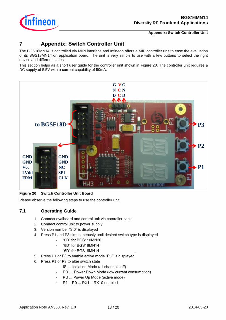
7 Appendix: Switch Controller Unit
The BGS18MN14 is controlled via MIPI interface and Infineon offers a MIPIcontroller unit to ease the evaluation of its BGS18MN14 on application board. The unit is very simple to use with a few buttons to select the right device and different states.
This section helps as a short user guide for the controller unit shown in Figure 20. The controller unit requires a DC supply of 5.5V with a current capability of 50mA.
Figure 20 Switch Controller Unit Board
Please observe the following steps to use the controller unit:
7.1 Operating Guide
1. Connect evalboard and control unit via controller cable
2. Connect control unit to power supply
3. Version number “S.0” is displayed
4. Press P1 and P3 simultaneously until desired switch type is displayed
- “0D” for BGS110MN20
- “8D” for BGS18MN14
- “6D” for BGS16MN14
5. Press P1 or P3 to enable active mode “PU” is displayed*
6. Press P1 or P3 to alter switch state
- IS … Isolation Mode (all channels off)
- PD … Power Down Mode (low current consumption)
- PU ... Power Up Mode (active mode)
- R1 – R0 ... RX1 – RX10 enabled
P3
P2
P1
to BGSF18D
G V G
N C N
D C D
GND GND
GND GND
Vcc NC
LVdd SPI
FRM CLK
BGS16MN14 Diversity RF Frontend Applications
Authors
Application Note AN368, Rev. 1.0 2014-05-23 19 / 20
8 Authors
Ralph Kuhn, Senior Staff Application Engineer of the Business Unit “RF and Protection Devices”
Andre Dewai, Senior Application Engineer of the Business Unit “RF and Protection Devices”

w w w . i n f i n e o n . c o m
Published by Infineon Technologies AG AN368


![DATA SHEET SKY13416-485LF: 0.1 to 3.8 GHz SP6T Antenna …€¦ · DATA SHEET • SKY13416-485LF: SP6T ANTENNA SWITCH Skyworks Solutions, Inc. • Phone [781] 376-3000 • Fax [781]](https://img.pdfslide.net/doc/110x75/5b9cf6e709d3f2de128b5149/data-sheet-sky13416-485lf-01-to-38-ghz-sp6t-antenna-data-sheet-sky13416-485lf.jpg)