Embed Size (px)
Citation preview
UNIVERSITÉ DE MONTRÉAL
BI-STABLE RADIOFREQUENCY RECTANGULAR WAVEGUIDE
SWITCH WITH MAGNETIC ACTUATION
HASSNA OUASSAL
DÉPARTEMENT DE GÉNIE ÉLECTRIQUE
ÉCOLE POLYTECHNIQUE DE MONTRÉAL
MÉMOIRE PRÉSENTÉ EN VUE DE L’OBTENTION
DU DIPLÔME DE MAÎTRISE ÈS SCIENCES APPLIQUÉES
(GÉNIE ÉLECTRIQUE)
AVRIL 2011
© Hassna Ouassal, 2011.
UNIVERSITÉ DE MONTRÉAL
ÉCOLE POLYTECHNIQUE DE MONTRÉAL
Ce mémoire intitulé:
BI-STABLE RADIOFREQUENCY RECTANGULAR WAVEGUIDE SWITCH WITH
MAGNETIC ACTUATION
Présenté par : OUASSAL Hassna
en vue de l’obtention du diplôme de : Maîtrise ès sciences appliquées
a été dûment accepté par le jury d’examen constitué de :
M. AKYEL Cevdet, Ph.D., président
M. LAURIN Jean-Jacques, Ph.D., membre et directeur de recherche
M.WU Ke, Ph.D., membre

iii
In the memory of my beloved father.

iv
ACKNOWLEDGMENTS
I wish to express my sincere appreciation and gratitude to my research
director, Professor Jean-Jacques Laurin for his scientific insight, invaluable guidance
and patience throughout the course of this research. I always felt that he was there
when I needed his help and that his door was always open. I consider myself
fortunate to have him as my supervisor, I learnt a great deal from him.
A special thanks to professors Cevdet Akyel, and Ke Wu for serving on my
thesis committee; the time and effort they put in reviewing my research work are
greatly appreciated.
I would like to acknowledge the assistance from all technical staffs at Poly-
Grames research centre. I also appreciate the help of all my friends and colleagues at
our research center. Furthermore, I would like to thank Nathalie Lévesque and
Ginette Desparois for their friendly and helpful service.
Extended thanks go to my mother, brothers and sisters for their
encouragement, support and love.
v
RÉSUMÉ
Ce mémoire présente une étude sur les utilisations possibles de nouveaux
types de commutateurs radiofréquences (RF) bistables dans la réalisation d’antennes
reconfigurables et de filtres à hautes fréquences. Ces commutateurs ont l’avantage
d’être légers (fabriqués sur une membrane très mince) et d’avoir une consommation
de puissance nulle dans les états stables. Les antennes reconfigurables et filtres
actuels consomment plus de puissance à cause de l’intégration des commutateurs
électroniques à base de semi-conducteurs ou MEMS qui nécessitent d'être polarisés
en permanence. Les commutateurs proposés peuvent apporter une alternative, surtout
dans des applications qui imposent des exigences strictes sur la consommation
d’énergie ou le poids. Puisque ces interrupteurs sont des composants non-
électroniques, ils présenteront moins d’interférences sur le comportement des
antennes reconfigurables, le problème est particulièrement important lorsque
plusieurs commutateurs sont intégrés à l’antenne.
Deux prototypes de configurations distinctes ont été fabriqués et testés
expérimentalement afin de vérifier leurs fonctionnements et d'évaluer leurs
performances. Le premier prototype est un commutateur membrane placé dans un
guide d'onde rectangulaire ouvert (antenne à ondes de fuites). Le deuxième est un
commutateur à réactance variable, placé dans un guide d'onde rectangulaire fermé.
Une des extrémités de la membrane est fixée à la paroi basse du guide et l’autre
extrémité est laissée libre. Les commutateurs sont réalisés à partir d’un substrat
flexible Pyralux de Dupont, composé d’une couche diélectrique (polyimide), laquelle
est recouverte d’une couche de cuivre sur une de ses deux faces. Les commutateurs
utilisent un système d'actionnement magnétique et ne dépensent de l’énergie que lors
du passage d’un état stable à l’autre.
vi
Le commutateur à membrane est utilisé pour la conception d’une antenne à
ondes de fuites commutable. Pour l’état ON, c'est-à-dire lorsque l’antenne rayonne,
les simulations et les mesures ont montré des résultats similaires. Pour l’état OFF,
c'est-à-dire lorsque l’antenne n’émet aucun rayonnement, une moins bonne
concordance a été observée. La raison est due à un mauvais contact électrique entre
la partie libre de l’interrupteur et la paroi haute du guide, lequel nécessiterait
quelques améliorations. Globalement, le concept d'une antenne commutable en
utilisant ce type de commutateur a été prouvé.
Le commutateur à réactance variable est intégré dans un guide d'onde
rectangulaire fermé afin de démontrer un filtre coupe bande « notch ». Les résultats
de mesures ont vérifié le concept en présentant des pertes d’insertion maximales de -
29.7 dB à la fréquence de coupure 11.1 GHz et une largeur de bande à -20 dB de
0.2 GHz. Deux commutateurs similaires ont été placés en cascade et une largeur de
bande de 0.9 GHz a été obtenue. Les temps de commutation de l’interrupteur ont été
mesurés et sont de 80 ms pour le passage à l’état OFF et de 3 ms pour le passage à
l’état ON.
vii
ABSTRACT
This M.Sc.A. thesis investigates the feasibility of using new types of bistable
waveguide switches to implement reconfigurable antennas and filters. These switches
have the advantages of being lightweight (made of very thin membrane) and have
zero power consumption in their steady states. Current reconfigurable antennas and
filters consume more power due to the integration of electronic switches;
semiconductor and MEMS. The proposed switches can provide an alternative,
especially in applications that impose stringent requirements on power consumption
or weight. Since these switches are non-electronic components, they present less
interference on the behaviour of reconfigurable antennas, the problem is particularly
important when multiple switches are integrated into the antenna.
Two prototypes of distinct configurations are implemented and
experimentally tested to verify and assess their performance. One is incorporated into
a leaky rectangular waveguide to provide antenna switchability feature and the other
is integrated into a closed rectangular waveguide to implement a switched filtering
structure. Both switches are built from a flexible membrane Pyralux Dupont,
composed of a dielectric layer (polyimide), which is covered with a layer of copper
on one side. They are attached to the bottom wall of the waveguide at one part and
free to move at the other part. They use a magnetic actuation system and consume
energy only when moving from one stable state to the other.
The measured radiation patterns and return losses of the switched leaky wave
antenna in the ON state agree quite well with the predictions obtained with a finite
elements simulation tool (HFSS). However, there is a noticeable difference between
the simulation and experimental results in the OFF state. This is mainly due to a non-
uniform physical contact between the edge of the switched membrane and the inner
viii
side of the waveguide’s broad wall. Overall, the results of this proof of concept look
promising. This technique provides an approach to implement reconfigurable antenna
using bistable membrane built on a dielectric substrate.
A stop-band “notch” filter is demonstrated using a variable reactance
membrane switch integrated into a closed rectangular waveguide. This structure can
be used in an application that requires channel selection. Using only one switch, the
measured S21 at the notch frequency of 11.1 GHz is -29.7 dB, with a 20 dB insertion
loss bandwidth of 0.2 GHz. By cascading two similar switches, the 20 dB stop-band
is as wide as 0.9 GHz. The measured switching times are 3ms for the transition from
the OFF to the ON state and 80 ms for the transition from the ON to the OFF state.
ix
CONDENSÉ EN FRANÇAIS
Le but du projet de recherche décrit dans ce mémoire est de concevoir et
d’intégrer un nouvel interrupteur radiofréquence (RF) bistable actionné par un
champ magnétique afin de déterminer son potentiel dans la réalisation d’antennes
reconfigurables et filtres à hautes fréquences pour les systèmes de
télécommunications. L’interrupteur proposé est construit sur une membrane flexible
et intégré dans un guide d’onde rectangulaire. Pour parvenir à cela, nous avons choisi
de développer deux configurations:
• Interrupteur dans un guide d’ondes rectangulaire ouvert (antenne à
ondes de fuite) ;
• Interrupteur dans un guide d’onde rectangulaire fermé.
Ce mémoire s’articule autour de cinq chapitres. Le premier chapitre présente
une vision globale des interrupteurs RF, leurs applications et leurs différents
principes de fonctionnement. Le deuxième chapitre, présente la conception de
l’interrupteur à membrane proposé. Le chapitre 3 porte sur l’intégration de
l’interrupteur bistable dans une antenne à ondes de fuite. Le chapitre 4 est consacré à
la réalisation d’une réactance variable placée dans un guide d’onde rectangulaire
fermé dans le but d’accomplir un filtre commutable. Le dernier chapitre conclut ce
mémoire et présente les travaux futurs.
Chapitre 1 : Introduction aux commutateurs RF
Ce chapitre présente de façon générale les commutateurs RF, le principe de
fonctionnement de leurs mécanismes d'actionnement et leurs applications.
x
Chapitre 2: Commutateur RF à base d’une membrane de polyimide
Ce chapitre présente les deux commutateurs réalisés. Leurs dimensions
physiques sont indiquées sur les Figures 2-1 et 2-2. La Figure 2-1 illustre le
commutateur membrane et la Figure 2-2 présente le commutateur à réactance
variable. Les interrupteurs sont constitués d’une membrane fixée à une extrémité, et
sont réalisés à partir d’un substrat flexible Pyralux de Dupont composé d’une
couche diélectrique (polyimide) recouverte de cuivre sur une face. Ils comportent une
partie fixe et une partie mobile. Pour le commutateur membrane, la partie mobile
comprend un ensemble de bandes de cuivres séparées par le diélectrique d’un côté et
une pièce magnétique (Metglas) de très haute perméabilité de l’autre. Pour le
commutateur à réactance variable, la partie mobile se compose d'une partie non
métallisée (couche de polyimide) partiellement recouverte d’une mince plaque de
matériau magnétique (Metglas).
Le substrat constituant le matériel de base de l’interrupteur comprend une
couche de diélectrique d’une épaisseur de 25.4 μm (polyimide) et d’une couche
métallique 35 μm (cuivre). Ce choix résulte d’un compromis entre la consommation
en courant et l’épaisseur de substrat. Avec une faible épaisseur de substrat,
l’interrupteur est instable lorsqu’il est soumis à des perturbations extérieures. Avec
une épaisseur plus importante, le commutateur est moins sensible mais nécessite
davantage de courant. Une analyse mécanique et magnétique a été élaborée afin de
déterminer une formulation analytique de la densité du champ magnétique nécessaire
pour un déplacement vertical de 2 mm de la partie mobile de l’interrupteur à
l’intérieur du guide. Les calculs ont montré que ce champ devait être de
12.61 millitesla (mT), tandis que les mesures ont montré qu’un champ de 12 mT était
suffisant.
xi
Chapitre 3: Antenne à ondes de fuite utilisant un commutateur membrane
L’objectif de ce chapitre est d’utiliser le commutateur membrane pour
commander une antenne à onde de fuite.
Dans un premier temps, des simulations avec le logiciel commercial d'éléments finis
HFSS (High Frequency Structure Simulator de la compagnie Ansoft) ont été
réalisées afin d’étudier le fonctionnement de l’interrupteur et l’effet de ce dernier sur
le rayonnement de l’antenne. Les simulations présentées sur la Figure 3-5, ont
montré de bons résultats. En effet, lorsque le commutateur est à la position
horizontale (ON) l’antenne rayonne. Lorsqu’il est à la position verticale (OFF)
l’antenne ne rayonne pas. Pour tester expérimentalement le système, un modèle
réduit de l’interrupteur a été placé dans un guide d’onde. Le test a montré qu’à l’état
OFF, l’interrupteur ne faisait pas un contact physique uniforme avec la surface du
guide. Par conséquent, l’idée de réaliser une antenne reconfigurable avec un réseau
de commutateurs n’a pas été poursuivie. Nous sommes alors tournés vers un autre
design, présenté sur la Figure 3-6. Dans ce nouveau design, l’antenne est composée
d’un guide d'onde rectangulaire de dimensions (900x80x9760) mils3 muni d’une
fente longitudinale et du commutateur membrane illustré à la même figure. La fente
est d'une longueur de 6760 mils et large de 200 mils. Notre guide n’étant pas de
dimensions standard, nous avons utilisés une transition permettant d’exciter le mode
TE10 comme l’indique la Figure 3-8(a). Un aimant permanent (très mince) produisant
une densité de flux de 2.55 mT est collé à la paroi du guide (Fig.3-10) pour assurer la
bi-stabilité, et deux bobines sont intégrées de chaque côté du guide pour permettre la
commutation. Lorsqu'un courant est appliqué à la bobine de l'état OFF, la membrane
est fléchie vers la position verticale (état stable 1) où elle établit un contact électrique
avec l’intérieur de la paroi et reste maintenu à l'état OFF par l'aimant permanent.
L'onde incidente est alors réfléchie et par conséquent, l'antenne ne rayonne pas. En
excitant momentanément la bobine de l'état ON, la membrane est déplacée à la
position horizontale (état stable 2). Le commutateur est à l’état ON et l'onde se
xii
propage le long de l’antenne où l'énergie fuit à travers la fente. L’antenne commute
avec un courant de 40 mA à l’état OFF et 140 mA à l’état ON, et l’interrupteur ne
consomme aucun courant dans les deux états. Lorsque le commutateur est à l’état
ON, les simulations des caractéristiques de l’antenne concordaient avec les mesures.
Toutefois, une moins bonne concordance a été observée pour l’état OFF. La raison
vient d’un mauvais contact électrique entre la membrane et la paroi du guide, lequel
nécessiterait quelques améliorations. Globalement, le concept d'une antenne
commutable par ce type de commutateur a été prouvé.
Chapitre 4 : Interrupteur membrane pour filtres de guide d’ondes commutable
Dans ce chapitre, le commutateur à réactance variable est intégré dans un
guide d'onde rectangulaire fermé (Fig. 4-1). Il est situé à une distance d = 50 mils
(Fig. 4-4) de la paroi latérale du guide d'onde. Nous avons conservé le même guide
d'onde ainsi que le même mécanisme de commutation et de bistabilité utilisés pour
démontrer l'antenne commutable. Cependant, une deuxième transition est ajoutée au
guide d'onde afin de mesurer la transmission. À l'état ON, la membrane est en
position basse et l'onde se propage à travers le guide. À l'état OFF, l’interrupteur est
actionné pour que la membrane réalise un contact diélectrique-métal avec la paroi
haute du guide. La réactance du guide d’onde est modifiée ce qui empêche une partie
du signal de se propager jusqu’au port de sortie. Il est à mentionner que pour éviter le
problème de contact électrique rencontré lorsque l’interrupteur était à l’état OFF dans
la partie «Antenne à ondes de fuite utilisant un commutateur membrane », le
commutateur dans sa position naturelle (état ON) est fixé de manière à ce que le côté
polyimide de la membrane fasse face à la paroi haute, tandis que son côté métallique
(Metglas) coïncide avec la paroi basse du guide d'onde. Dans les simulations HFSS,
l'interrupteur est modélisé comme un conducteur électrique parfait. Donc, A l'état
OFF, un écart de 1 mil (épaisseur polyimide) sépare la paroi métallique haute du
guide et la membrane.
xiii
Cet interrupteur commute à partir de 30 mA en un temps de 80 ms pour l’état
OFF, et de 110 mA en un temps de 3 ms pour l’état ON. À l’état OFF, le
commutateur présente un comportement de filtre coupe bande. À la fréquence de
coupure égale à 10.8 GHz, les pertes d’insertion sont de 33 dB. La largeur de bande
pour une perte d'insertion de 20 dB est de 0.2 GHz. Ces résultats sont comparés avec
les valeurs mesurées et une bonne concordance à été observée. Cependant, un léger
décalage de la fréquence de coupure est observé. En effet, la fréquence de coupure
est mesurée à 11.1 GHz au lieu de 10.8 GHz. Cela peut provenir d’un léger décalage
dans le positionnement de l’interrupteur lors de son intégration dans le guide. En
effet, comme le montre la Figure 4.5, un petit décalage de l'emplacement de
l'interrupteur provoque une variation de la fréquence de coupure.
Il serait avantageux d'ajouter des commutateurs multiples pour obtenir une
bande passante plus large. Pour ce faire, deux commutateurs similaires ont été placés
en cascade dans le guide d’onde comme le présente la Figure 4-10. En commutant
l’un des interrupteurs à l’état OFF, la largeur de bande simulée et mesurée est de 0.2
GHz. En forçant les deux interrupteurs à l’état OFF, la largeur de bande simulée et
mesurée est de 0.9 GHz. On peut remarquer que les valeurs simulées concordent
avec celles mesurées. Par contre, dans le cas ou les deux interrupteurs sont à l’état
OFF, les pertes de retour mesurées dans la bande passante sont moins bonnes que
celles modélisées. Ceci peut être dû à des pertes dans les transitions entre guides
d'ondes de tailles différentes.
Finalement une discussion sur les améliorations possibles a été élaborée. Le
temps de commutation de l’interrupteur à l’état OFF est long par rapport à celui à
l’état ON. Ceci est dû à des rebonds (Fig. 4-15) de l’interrupteur qui apparaissent
avant qu’il se stabilise. Il serait intéressant de minimiser ce temps de commutation en
utilisant par exemple un matériau magnétique de plus haute perméabilité, ce qui
réduirait la tension requise ainsi que le temps de commutation. En ce qui concerne

xiv
l’antenne commutable, les efforts futurs doivent être dirigés vers l'élaboration d'une
technique pour améliorer le contact électrique lors de l’état OFF. Il serait aussi
intéressant de réaliser un filtre ajustable en fréquence. Nous avons observé qu’en
modifiant la dimension physique de la membrane, une modification de la fréquence
de coupure pouvait être obtenue (Figs. 4-2 et 4-3). Aussi, en cascadant plusieurs
membranes à réactances variables de dimensions différentes à l’intérieur du guide
d’onde, la fréquence de coupure peut être modifiée dépendant de l’interrupteur
actionné.

xv
CONTENTS
ACKNOWLEDGMENTS ......................................................................................... IV
RÉSUMÉ……. ............................................................................................................ V
ABSTRACT… .......................................................................................................... VII
CONDENSÉ EN FRANÇAIS ................................................................................... IX
CONTENTS ………………………………………………………………………..XV
LIST OF TABLES ................................................................................................ XVIII
LIST OF FIGURES ................................................................................................ XIX
LIST OF ABBREVIATIONS AND NOTATIONS ............................................. XXIII
INTRODUCTION ....................................................................................................... 1
CHAPTER 1. INTRODUCTION TO RF SWITCHES .......................................... 4
1.1 RF Switches and Applications ..................................................................... 4
1.2 Principles of Various Types of Actuation .................................................. 11
1.2.1 Electrostatic actuation ............................................................................ 11
1.2.2 Magnetic actuation ................................................................................. 13
1.2.3 Piezoelectric actuation ........................................................................... 16
1.2.4 Thermal actuation .................................................................................. 18
1.3 Summary of the Actuation Mechanisms .................................................... 19
1.4 Discussion about Power Handling and Linearity Capabilities................... 20
1.4. 1 Low and high power switches ............................................................ 20
1.4.2 Nonlinearity problem ............................................................................. 21
CHAPTER 2. RF SWITCHES USING A POLYIMIDE MEMBRANE ............. 24
2.1 Introduction ................................................................................................ 24
2.2 Switches Design ......................................................................................... 25
2.3 Material Choice .......................................................................................... 28
2.4 Principle of Operation ................................................................................ 28
2.5 Mechanical Analysis .................................................................................. 30

xvi
2.6 Magnetic Analysis ..................................................................................... 34
2.7 Magnetic Field Density Calculation .......................................................... 35
2.8 Experimental Validation ............................................................................ 37
2.9 Conclusion ................................................................................................. 37
CHAPTER 3. LEAKY WAVE ANTENNA USING A MEMBRANE SWITCH 39
3.1 Introduction ................................................................................................ 39
3.2 Leaky Waveguide Antenna Theory ........................................................... 39
3.3 Switchable Antenna Design 1 .................................................................... 41
3.4 Switchable Antenna Design 2 .................................................................... 45
3.5 Switchable Antenna Structure and Functionality....................................... 48
3.6 Results ........................................................................................................ 51
3.7 Discussions ................................................................................................ 59
3.7.1 Effect of switch contact .......................................................................... 59
3.7.2 Effect of switch proximity to the slot ..................................................... 60
3.7.3 Effect of strips width .............................................................................. 61
3.8 Summary .................................................................................................... 62
CHAPTER 4. MEMBRANE-BASED SWITCHED WAVEGUIDE FILTER .... 63
4.1 Introduction ................................................................................................ 63
4.2 Design and Operation................................................................................. 64
4.3 Effect of Switch Length and Position ........................................................ 66
4.3.1 Effect of varying the length of the movable beam ................................. 66
4.3.2 Effect of the switch location .................................................................. 68
4.4 Simulations and Measurements Results ..................................................... 70
4.4.1 One switch integration ........................................................................... 70
4.4.2 Two switches incorporation ................................................................... 74
4.4.3 Switching time measurement ................................................................. 78
4.5 Conclusion ................................................................................................. 80
CHAPTER 5. CONCLUSIONS ............................................................................ 82

xvii
5.1 Thesis Contributions .................................................................................. 82
5.2 Future Work ............................................................................................... 83
REFERENCES........................................................................................................... 85

xviii
LIST OF TABLES
Table 1.1 Performance comparison of RF MEMS, PIN diode, and FET based on
[16]. ...................................................................................................................... 7
Table 1.2 Comparison of varactors technologies [24][25]. ....................................... 11
Table 2.1 Parameters used to calculate the magnetic flux density. ............................ 36

xix
LIST OF FIGURES
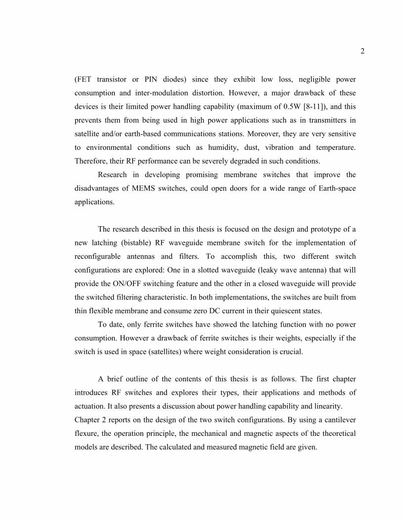
Figure 1-1 Series switches developed by (a) Analog Devices [12] and (b) Lincoln
Laboratory [13] with their equivalent circuits. .................................................... 5
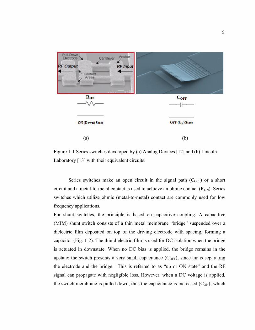
Figure 1-2 Shunt switch developed by Rytheon [14] with the equivalent circuit. ....... 6
Figure 1-3 A simplified block diagram of a satellite payload [17]. ............................. 8
Figure 1-4 Parallel plate capacitor. ........................................................................... 12
Figure 1-5 Structure of a series electrostatic switch [26]. .......................................... 12
Figure 1-6 Magnetic latching switch [27]. ................................................................. 13
Figure 1-7 Illustration of Lorentz force principle [28]. ............................................. 15
Figure 1-8 cantilever switch based on Lorentz force [29]. ........................................ 15
Figure 1-9 Illustration of piezoelectric actuation in a unimorph cantilever for two
modes of operation. (a) transverse or d31 mode. (b) longitudinal or d33 mode. E =
Electric field, P = Polarization, S = Strain, V = Voltage. .................................. 17
Figure 1-10 An Example of piezoelectric microswitch [33]. ..................................... 18
Figure 1-11 Martensite and austenite phases [35]. .................................................... 19
Figure 1-12 Spectral display of non-linearity. ........................................................... 22
Figure 1-13 Simplified block diagram of antenna subsystem. ................................... 23
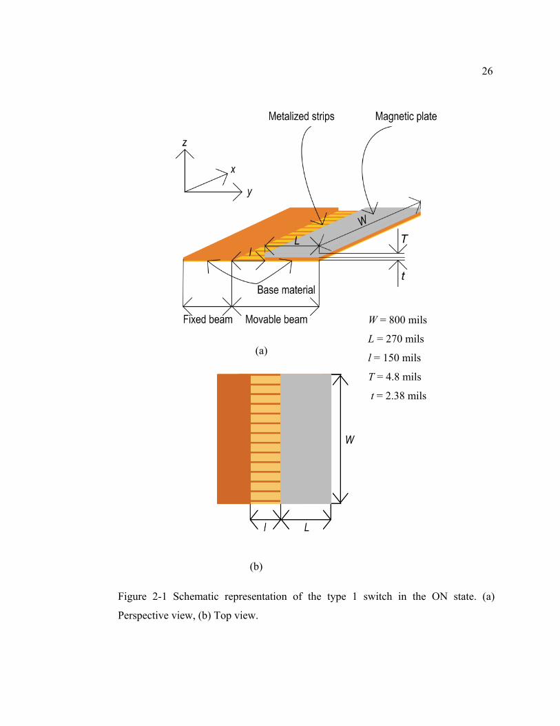
Figure 2-1 Schematic representation of the type 1 switch in the ON state. (a)
Perspective view, (b) Top view.......................................................................... 26
Figure 2-2 Schematic representation of the type 2 switch in the ON state. (a)
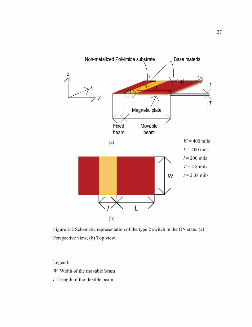
Perspective view, (b) Top view.......................................................................... 27
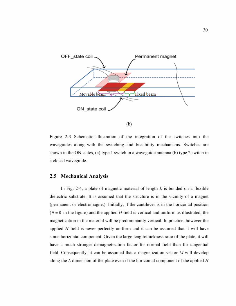
Figure 2-3 Schematic illustration of the integration of the switches into the
waveguides along with the switching and bistability mechanisms. Switches are
shown in the ON states, (a) type 1 switch in a waveguide antenna (b) type 2
switch in a closed waveguide. ............................................................................ 30
Figure 2-4 Cantilever switch under an applied magnetic field. ................................. 31
Figure 2-5 Simplified mechanical model of the cantilever switch. ........................... 31
Figure 2-6 Schematic illustration of the cantilever switch under an applied torque. . 32
xx
Figure 2-7 Flexible beams cross-sections: (a) region of strips and (b) polyimide
beam. .................................................................................................................. 33
Figure 2-8 Presentation of the magnetic charges, the uniform magnetic field lines and
their effect on the displacement of the cantilever switch. .................................. 34
Figure 2-9 Teslameter probe used to measure the magnetic field density generated
by the coil that causes the cantilever to move to the top wall of the waveguide.
............................................................................................................................ 37
Figure 3-1 Leaky wave structure showing principal beam angle. ............................. 40
Figure 3-2 Slotted waveguide with two flexible plates, one is in the up position and
the other is in the down position. The antenna is in the ON state. ..................... 42
Figure 3-3 Simulated EΦ field pattern in XZ plane (H-plane) in the ON and OFF
states for antenna geometry 1............................................................................. 43
Figure 3-4 Slotted waveguide with one switch in OFF state: geometry 2. ................ 44
Figure 3-5 Simulated EΦ field pattern in H-plane (XZ plane) of the switch operations
(ON/OFF) for antenna geometry 2. .................................................................... 44
Figure 3-6 A screen shot of the HFSS antenna model showing the arrangement of the
switch and its dimensions. Drawing is not to scale............................................ 46
Figure 3-7 Upper side of the waveguide showing the slot dimensions. .................... 47
Figure 3-8 (a) WR90 adaptor and tapered transition (b) Simulated S-parameter
results of the transition. ...................................................................................... 48
Figure 3-9 principle of antenna operation. ................................................................. 49
Figure 3-10 (a) A Photograph of the fabricated antenna with integrated coils and
permanent magnet, (b) A photograph of the fabricated switch inside the
waveguide. ......................................................................................................... 50
Figure 3-11Return loss simulations for both states of the switchable antenna. ......... 52
Figure 3-12 Return loss measurements for both states of the switchable antenna. ... 52
Figure 3-13 Simulated and measured normalized gain in H plane for ON state at 10
GHz. ................................................................................................................... 53
xxi
Figure 3-14 A 3-D simulated HFSS realized gain polar pattern (in linear scale). ..... 54
Figure 3-15 Simulated realized gain (XZ plane, Φ = 0) for ON and OFF states at 10
GHz .................................................................................................................... 55
Figure 3-16 Measured gain (H plane) for ON and OFF states at 10 GHz. ................ 56
Figure 3-17 Measured gain (H plane) for ON and OFF states at different frequencies.
............................................................................................................................ 57
Figure 3-18 Simulated EΦ field patterns (a) in YZ and (b) XZ planes. .................... 58
Figure 3-19 A front view (YZ plane) of the switch inside the waveguide showing a
gap between the surface broadwall and the beam. The switch is in the OFF state.
............................................................................................................................ 59
Figure 3-20 Effect of switch contact on realized gain. .............................................. 60
Figure 3-21 EΦ field patterns (XZ plane) for OFF state at different switch positions.
Parameter d is the distance between the switching plate and the waveguide input
port. .................................................................................................................... 61
Figure 3-22 EΦ field patterns (XZ plane) for OFF state at different strip widths. ..... 62
Figure 4-1 Membrane switch geometry: (a) screen shot of the HFSS model of the
switch inside the waveguide. (b) Its schematic diagram. The design parameters
are labeled within the drawing. (c) A photograph of the fabricated switch set in
the waveguide. ................................................................................................... 65
Figure 4-2 Simulated S-parameters for the waveguide, showing the effect of
modifying the length of the dielectric beam. The switch is in the up position. . 67
Figure 4-3 Simulated S-parameters for the waveguide, showing the effect of
modifying the length of the metallic plate. The switch is in the up position. .... 68
Figure 4-4 Switch position in the waveguide............................................................. 69
Figure 4-5 Simulated S-parameters for the waveguide with variation in the switch
position. The Switch is in the up position. ......................................................... 69
Figure 4-6 Measured S-parameters of the waveguide with switch in the ON state and
without switch. ................................................................................................... 71
xxii
Figure 4-7 Measured S-parameters when the switch is OFF. 3 dB transitions losses
were assumed and subtracted. ............................................................................ 72
Figure 4-8 Simulated S-parameters when the switch is ON. ..................................... 73
Figure 4-9 Simulated S-parameters when the switch is OFF..................................... 74
Figure 4-10 Switches arrangement in the waveguide. Drawing is not to scale. ...... 76
Figure 4-11 Simulated S-parameters when the switches are OFF, showing the effect
of switch operation on the bandwidth. ............................................................... 77
Figure 4-12 Measured S-parameters when the switches are OFF, showing the effect
of switch operation on the bandwidth. ............................................................... 78
Figure 4-13 Switching time measurement setup. ...................................................... 79
Figure 4-14 Detected RF signal when the switch is ON and OFF. ........................... 80
Figure 4-15 Illustration of the measured switching time: (a) toff and (b) ton. ............ 80

xxiii
LIST OF ABBREVIATIONS AND NOTATIONS
SAR Synthetic Aperture Radar
RF Radio-Frequency
MEMS Micro-Electro-Mechanical Systems
FET Field-Effect-Transistor
PIN P-Type Intrinsic N-Type
DC Direct Current
MIM Metal-Insulator-Metal
GaAs Gallium Arsenide
MESFETs Metal-Semiconductor Field-Effect-Transistors
FETs Field-Effect-Transistors
IDC InterDigital Capacitors
Q Quality Factor
PEC Perfect Electric Conductor
μr Relative Permeability
1
INTRODUCTION
Human involvement in space exploration and Earth science will bring new
advanced sensing and communication systems to allow for higher data transmission
rates and exploration of planets like Mars, Moon and beyond, as well as for more
accurate earth and planetary remote sensing activities. Taking into account the cost of
launching hardware into space (about $20K per kg), also the payload fairing space
limitations, there is a need in finding new methods of fabricating large antennas which
present lighter weight than conventional antennas to circumvent these limitations. Such
large antennas [1] would seem to be impossible to launch into space, unless one
considers innovative materials and lightweight structures that can be compactly
packaged for launch and reliably deployed once in orbit.
To address this issue, deployable structures using inflatable or thin-membranes
have presented a new possibility to satisfy the aforementioned requirements. This type
of space structures, because of the use of membranes and lightweight components,
provide a means to reduce the mass launch vehicle, stowage volume and overall
program cost associated with the payload systems.
Membranes are made of thin, ultra lightweight polyimide1 film. This implies, low
Young’s modulus, highly flexible material. Their low bending stiffness, allows them to
be found in either tensioned or inflated configurations. Applications of such membranes
include SAR membrane antennas [2-5], earth radiometers [6], solar sails [7], and
deployable solar arrays. The missions may include deep space, low earth orbit or other
Solar System Planets and satellites.
Additionally, these sheet-like membranes can also be used to fabricate
prospective RF membrane switches. As example, RF MEMS switches which have been
proven to be the most valuable technology compared to their solid-state counterparts
1 The polyimide membranes used in this work are commercialized by DuPont under the names Kapton®
and Pyralux®.
2
(FET transistor or PIN diodes) since they exhibit low loss, negligible power
consumption and inter-modulation distortion. However, a major drawback of these
devices is their limited power handling capability (maximum of 0.5W [8-11]), and this
prevents them from being used in high power applications such as in transmitters in
satellite and/or earth-based communications stations. Moreover, they are very sensitive
to environmental conditions such as humidity, dust, vibration and temperature.
Therefore, their RF performance can be severely degraded in such conditions.
Research in developing promising membrane switches that improve the
disadvantages of MEMS switches, could open doors for a wide range of Earth-space
applications.
The research described in this thesis is focused on the design and prototype of a
new latching (bistable) RF waveguide membrane switch for the implementation of
reconfigurable antennas and filters. To accomplish this, two different switch
configurations are explored: One in a slotted waveguide (leaky wave antenna) that will
provide the ON/OFF switching feature and the other in a closed waveguide will provide
the switched filtering characteristic. In both implementations, the switches are built from
thin flexible membrane and consume zero DC current in their quiescent states.
To date, only ferrite switches have showed the latching function with no power
consumption. However a drawback of ferrite switches is their weights, especially if the
switch is used in space (satellites) where weight consideration is crucial.
A brief outline of the contents of this thesis is as follows. The first chapter
introduces RF switches and explores their types, their applications and methods of
actuation. It also presents a discussion about power handling capability and linearity.
Chapter 2 reports on the design of the two switch configurations. By using a cantilever
flexure, the operation principle, the mechanical and magnetic aspects of the theoretical
models are described. The calculated and measured magnetic field are given.

3
Chapter 3 discusses the integration of a membrane switch into a leaky-wave antenna.
Several design solutions to form a switchable antenna are presented. The principle of
operation of the fabricated prototype is given. Theoretical and experimental results are
presented.
Chapter 4 describes and demonstrates a stop-band (notch) filter based on a variable
reactance membrane in a closed rectangular waveguide.
The last chapter provides a summary of the thesis and discussion of future work.

4
CHAPTER 1. INTRODUCTION TO RF SWITCHES
This chapter provides an introduction to RF switches. Different types of
switch are discussed, along with an emphasis on their applications. Then, a detailed
survey of actuation mechanisms is presented, which includes the operation principles
and example of some typical devices. The remaining part of this chapter discusses
the power handling capability of commonly used switches and describes the
nonlinear behavior caused by RF switches and other passive components.
1.1 RF Switches and Applications
RF switches are passive components that isolate RF signals when they are
OFF, and allow RF signals to pass through when they are ON. Typical arrangements
of these switches are single-pole single-throw (SPST), single-pole double-throw
(SPDT), and single-pole quad-throw (SPQT), often with each arrangement using
series and/or shunt combinations. Figure 1-1 shows two series MEMS switches
developed by Analog Devices [12] and Lincoln Laboratory [13] respectively with
their equivalent circuit model.
5
(a) (b)
Figure 1-1 Series switches developed by (a) Analog Devices [12] and (b) Lincoln
Laboratory [13] with their equivalent circuits.
Series switches make an open circuit in the signal path (COFF) or a short
circuit and a metal-to-metal contact is used to achieve an ohmic contact (RON). Series
switches which utilize ohmic (metal-to-metal) contact are commonly used for low
frequency applications.
For shunt switches, the principle is based on capacitive coupling. A capacitive
(MIM) shunt switch consists of a thin metal membrane “bridge” suspended over a
dielectric film deposited on top of the driving electrode with spacing, forming a
capacitor (Fig. 1-2). The thin dielectric film is used for DC isolation when the bridge
is actuated in downstate. When no DC bias is applied, the bridge remains in the
upstate; the switch presents a very small capacitance (COFF), since air is separating
the electrode and the bridge. This is referred to as “up or ON state” and the RF
signal can propagate with negligible loss. However, when a DC voltage is applied,
the switch membrane is pulled down, thus the capacitance is increased (CON); which
6
is equivalent to an RF short circuit. This is also referred to as “the down or OFF
state” and the entire incident RF signal is reflected. Large “OFF” state capacitance
and small negligible “ON” state capacitance are required to produce large capacitive
ratio (CON/COFF) in order to achieve high tenability.
Figure 1-2 Shunt switch developed by Rytheon [14] with the equivalent circuit.
There are many parameters that are more or less critical when evaluating a
switch performance. Such parameters are: insertion loss, isolation, DC power
consumption, power handling capability, linearity, and switching speed. Traditional
switches that include waveguide and coaxial switches show low insertion loss, high
isolation, and good power handling capability but are power-consuming and slow.
Solid-state electronic devices such as PIN diodes and GaAs MESFETs are used for
their high switching speed, commercial availability, and low cost. However, at signal
frequencies above 1 GHz, they exhibit large insertion loss in the ON state and poor
isolation in the OFF state [15]. MEMS switches offer very low loss, high isolation
and extreme linearity. However, disadvantages include increased actuation voltages,

7
slower switching speeds, and limited power handling. Table 1.1 shows a comparison
between PIN, FET and MEMS switch technology [16].
Table 1.1 Performance comparison of RF MEMS, PIN diode, and FET based on
[16].
Parameter RF MEMS PIN-Diode FET
Voltage (V) 20-80 ± 3-5 3-5
Current (mA) 0 3-20 0
Power consumption (mW) 0.05-1 5-100 0.05 – 0.1
Switching time 1-300 μs 1-100 ns 1-100 ns
Up-state capacitance (fF) 1-6 40-80 70-140
Series resistance (Ώ) 0.5 – 2 2-4 4-6
Capacitance ratio 40-500 10 n/a
Isolation (1-10 GHz) Very high High Medium
Isolation (10 – 40 GHz) Very high Medium Low
Isolation (60 – 100 GHz) High Medium None
Loss dB (1-100 GHz) 0.05-0.2 0.3-1.2 0.4-2.5
Power handling (W) <1 <10 <10
RF switches are employed in a variety of commercial, aerospace and defence
application areas including satellite communications systems, wireless
communications systems and radar. One example is a simplified block diagram of a
satellite payload (Fig. 1-3). It consists of receive/transmit antenna, a beam forming
network (BFN), input filter assembly (IFA), high gain receiver (RCV), input and
output multiplexers, high power amplifiers (HPA) as well as several switch matrices.
In a satellite system of this type, switches are used in the form of the switch matrices
to provide redundancy or signal routing. The receiver input/output and low power
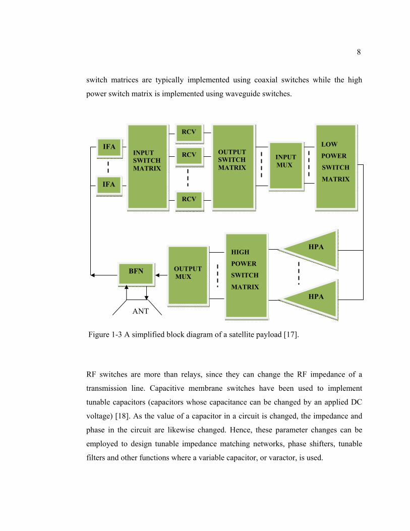
8
switch matrices are typically implemented using coaxial switches while the high
power switch matrix is implemented using waveguide switches.
Figure 1-3 A simplified block diagram of a satellite payload [17].
RF switches are more than relays, since they can change the RF impedance of a
transmission line. Capacitive membrane switches have been used to implement
tunable capacitors (capacitors whose capacitance can be changed by an applied DC
voltage) [18]. As the value of a capacitor in a circuit is changed, the impedance and
phase in the circuit are likewise changed. Hence, these parameter changes can be
employed to design tunable impedance matching networks, phase shifters, tunable
filters and other functions where a variable capacitor, or varactor, is used.
ANT
BFN
INPUT MUX
LOW
POWER
SWITCH
MATRIX
OUTPUT MUX
HIGH
POWER
SWITCH
MATRIX
IFA
IFA
OUTPUT SWITCH MATRIX
INPUT SWITCH MATRIX
RCV
RCV
RCV
HPA
HPA
9
Microwave tunable filters can be divided into two groups, filters with discrete
tuning, and filters with continuous tuning. Filter configurations presenting a discrete
tuning generally use PIN diodes or MEMS switches. On the other hand, filter
topologies using varactor diodes, MEMS capacitors, ferroelectric materials or
ferromagnetic materials are frequently used to obtain a continuous tuning device.
Zhang & Mansour, 2007 [19], have reported a tunable slotline resonators printed on
a microstrip ground plane to make a low pass filter. The tunability was obtained by
actuating arrays of RF MEMS switches located on the slots between ON and OFF
states, thereby changing the cutoff frequency of the low pass filter.
Ocera et al. 2006 [20], reported a microstrip bandpass filter using hairpin resonators
with direct contact cantilever switches on the end of the resonators. The cantilever
switches are used to enlarge the hairpin resonators when the switches are in the ON
state, thus tuning the device center frequency.
Ong & Okoniewski [21], also reported a four-resonator microwave bandpass filter.
The filter frequency response is switched using MEMS cantilever capacitive
switches. The filter has insertion losses of 0.6 and 1.3 dB and the frequency response
tunes from 16.025 to 13.675 GHz.
Ferroelectric materials can change permittivity values proportionally to an
applied DC electric field. Barium Strontium Titanate, ((Bax,Sr1-x)TiO3),(BST), one of
the most intensively studied ferroelectric, represents the state-of-the-art technology
for tuning microwave devices. BST is used as a dielectric for fabricating tunable
capacitors. It has strong electric-field-dependent permittivity, high power handling
capability, and a high value of dielectric constant (300 at room temperature) which
allows the fabrication of capacitors with very small footprints. Some works on
tunable filters using BST varactors, both in parallel plate (MIM) and InterDigital
Capacitors (IDC) configurations are reported below.
10
Nath et al. [22] have reported a tunable third-order combline band pass filter using
thin-film BST IDC. The band pass filter achieved 16% tunability (2.44 to 2.84 GHz)
upon the application of 0-200 V bias. The insertion loss was 5 dB at zero bias to 3 dB
at 200 V.
Tombak et al. [23] reported tunable lowpass and bandpass filters based on parallel
plate BST thin film capacitors. The LPF achieved 40% tunability (120-170 MHz)
with the application of 0-9 V DC bias and an insertion loss of 2 dB. The BPF showed
a tunability of 57% (176-276 MHz) with 0–6 V bias. The passband insertion loss of
the BPF was measured to be 3 dB.
Thus, there exist tradeoffs between the IDC and the MIM structures as stated
in these references. In a MIM structure, a BST thin film is sandwiched between two
metallic layers, while in an IDC structure, the BST film is directly deposited on the
appropriate substrate and metal lines form interdigitated structure on the thin film
surface. In general IDCs have small tuning range (as a large part of the electric field
passes through air and not the dielectric) and a higher bias voltage is required.
Nevertheless, they have better power handling capability. MIMs, on the other hand
can achieve maximum tunabillity (electric fields are better confined in the film) at
low power level, but at the expense of reduced linearity. Other varactors technologies
are currently competing with BST varactors, such as diode varactors and MEMS
varactors. MEMS varactors have very high Q value. Yet, they have some
disadvantages that include low tunability, slow switching speed and high bias voltage
(10 to 100 volts). They also face practical challenges of reliability and expensive
hermetic packaging. Diode varactors are highly tunable, however they suffer from Q
degradation at higher frequencies. A comparison of the aforementioned varactor
technologies is shown in Table 1.2.

11
Table 1.2 Comparison of varactors technologies [24][25].
Properties Varactor diode MEMS varactor Ferroelectric varactor
Tunability High Low High
Quality factor Moderate High Moderate
Biasing voltage Medium High Medium
Tuning speed Fast Slow Fast
Power handling low Moderate High
Cost Moderate/High High Low
Packaging Hermetic Hermetic Standard
It is apparent that each technology has its own pros and cons, therefore
depending on the application one technology will perform better than other.
Applications that favour thin film BST varactors are: 1) Ones requiring rapid,
continuous tuning at low voltage, and 2) frequency conversion devices, such as
frequency multipliers that exploit the “fast” capacitive non-linearity.
1.2 Principles of Various Types of Actuation
1.2.1 Electrostatic actuation
Electrostatic actuation is based on the principle of charge attraction. Consider
two parallel plates (Fig. 1-4) with an applied voltage (V). The capacitance (C)
between the plates is given by:
0 r AC 1.1d
ε ε=
Where ε0 and εr are the free-space and relative permittivities respectively, A is the
area of the parallel plates and d is the distance between the plates. When a voltage is
applied between the two plates, the electrostatic energy stored in the capacitor is
defined as:
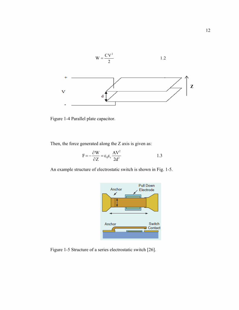
12
2CVW 1.2
2=
Figure 1-4 Parallel plate capacitor.
Then, the force generated along the Z axis is given as:
2
0 r 2
W AVF 1.3Z 2d
∂= − = ε ε
∂
An example structure of electrostatic switch is shown in Fig. 1-5.
Figure 1-5 Structure of a series electrostatic switch [26].
Z
13
In this type of series cantilever switch, the bottom electrode is placed underneath the
cantilever. By applying an actuation voltage between the membrane and the bottom
electrode, an electrostatic force is created to pull the membrane down; the switch
ultimately closes when the actuation voltage exceeds the threshold voltage (pull-in
voltage). Once the switch closes, the DC electric field will be higher due to the
smaller gap between the membrane and bottom electrode.
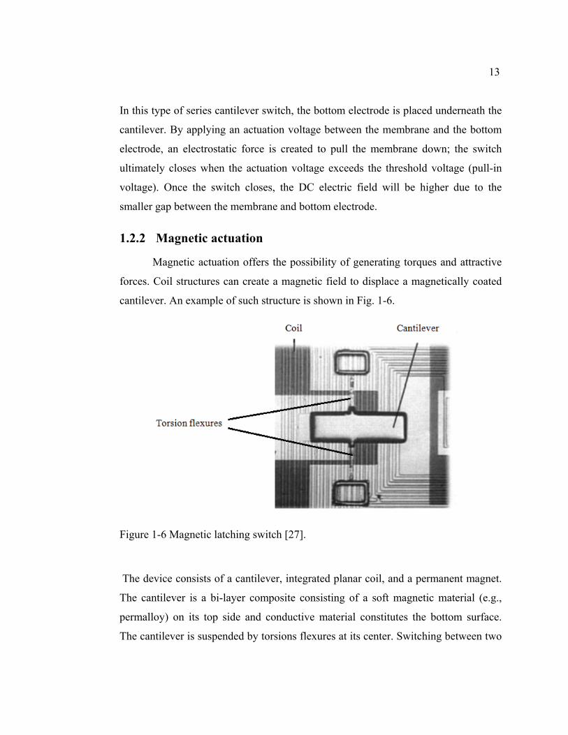
1.2.2 Magnetic actuation
Magnetic actuation offers the possibility of generating torques and attractive
forces. Coil structures can create a magnetic field to displace a magnetically coated
cantilever. An example of such structure is shown in Fig. 1-6.
Figure 1-6 Magnetic latching switch [27].
The device consists of a cantilever, integrated planar coil, and a permanent magnet.
The cantilever is a bi-layer composite consisting of a soft magnetic material (e.g.,
permalloy) on its top side and conductive material constitutes the bottom surface.
The cantilever is suspended by torsions flexures at its center. Switching between two
14
stable states is accomplished by energizing the planar coil underneath the cantilever.
The switching coil current produces a magnetic field that reverses the direction of the
cantilever. Once switched, it is latched by a permanent magnet.
An advantage of this approach is that power is only required while changing the
latched state of the device.
The designs proposed in this thesis are also based on this actuation principle. The
main difference between this design and the one that will presented in chapters 2 is
that our proposed cantilever is fixed at one end and is free to deflect at the opposite.
Besides, two coils are used to displace the switching cantilever.
Magnetic actuation can also be done using Lorentz force principle. This
principle states that charged particles moving perpendicular to a magnetic field will
experience a Lorentz force, that is F q v x B=r rr
. Where q is the charge of the particle,
v is its speed vector, B is the magnetic flux density.
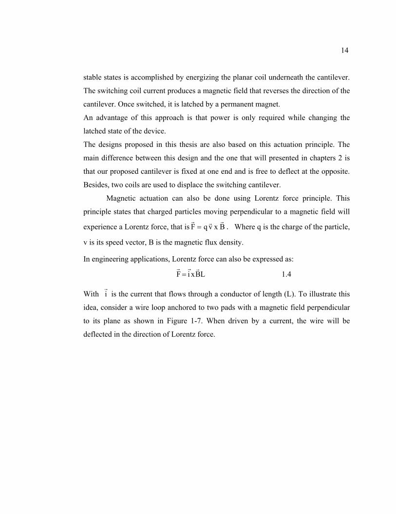
In engineering applications, Lorentz force can also be expressed as:
F i xBL 1.4=r r r
With ir
is the current that flows through a conductor of length (L). To illustrate this
idea, consider a wire loop anchored to two pads with a magnetic field perpendicular
to its plane as shown in Figure 1-7. When driven by a current, the wire will be
deflected in the direction of Lorentz force.
15
Figure 1-7 Illustration of Lorentz force principle [28].
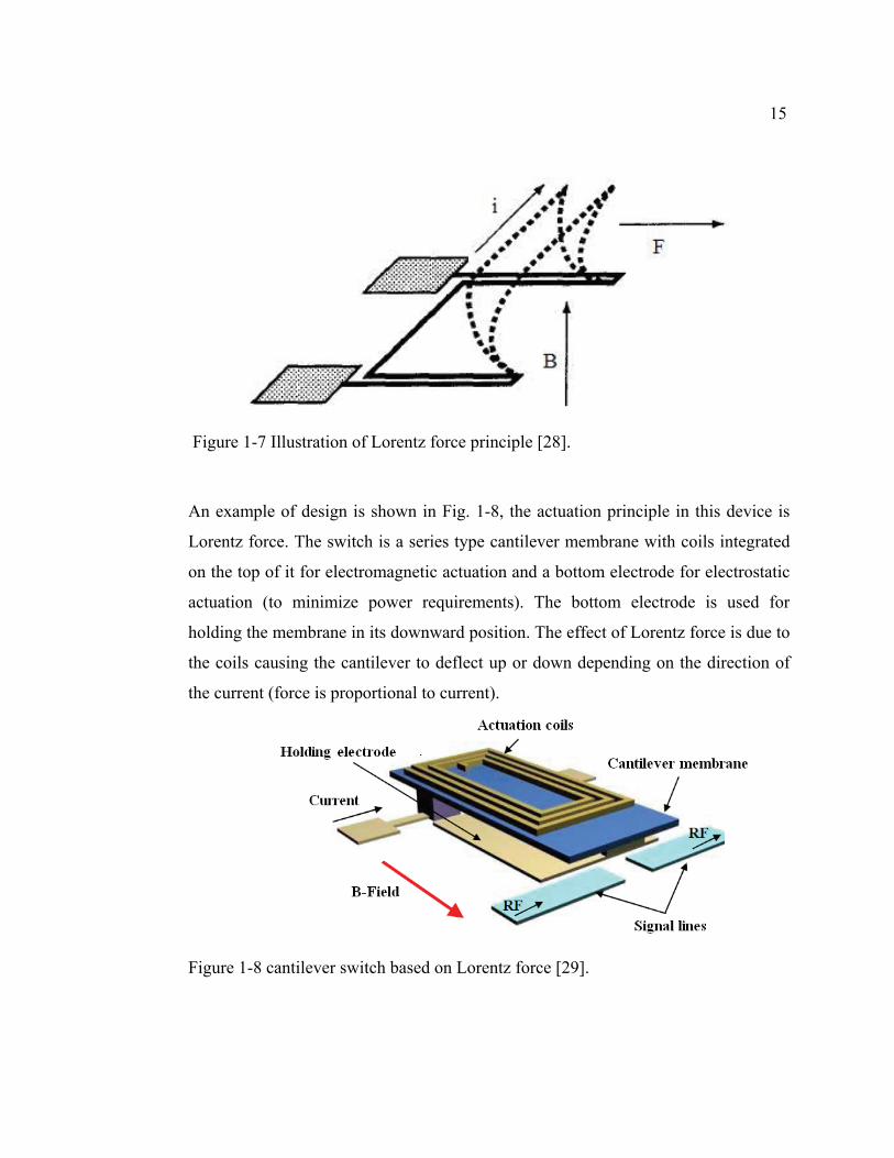
An example of design is shown in Fig. 1-8, the actuation principle in this device is
Lorentz force. The switch is a series type cantilever membrane with coils integrated
on the top of it for electromagnetic actuation and a bottom electrode for electrostatic
actuation (to minimize power requirements). The bottom electrode is used for
holding the membrane in its downward position. The effect of Lorentz force is due to
the coils causing the cantilever to deflect up or down depending on the direction of
the current (force is proportional to current).
Figure 1-8 cantilever switch based on Lorentz force [29].
16
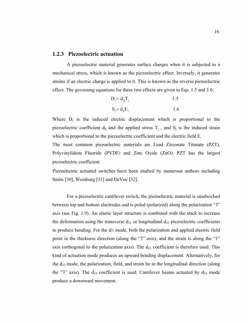
1.2.3 Piezoelectric actuation
A piezoelectric material generates surface charges when it is subjected to a
mechanical stress, which is known as the piezoelectric effect. Inversely, it generates
strains if an electric charge is applied to it. This is known as the reverse piezoelectric
effect. The governing equations for these two effects are given in Eqs. 1.5 and 1.6:
i ij jD d T 1.5=
j ij iS d E 1.6=
Where Di is the induced electric displacement which is proportional to the
piezoelectric coefficient dij and the applied stress Tj , and Sj is the induced strain
which is proportional to the piezoelectric coefficient and the electric field E.
The most common piezoelectric materials are Lead Zirconate Titanate (PZT),
Polyvinylidene Fluoride (PVDF) and Zinc Oxide (ZnO). PZT has the largest
piezoelectric coefficient.
Piezoelectric actuated switches have been studied by numerous authors including
Smits [30], Weinburg [31] and DeVoe [32].
For a piezoelectric cantilever switch, the piezoelectric material is sandwiched
between top and bottom electrodes and is poled (polarized) along the polarization “3”
axis (see Fig. 1.9). An elastic layer structure is combined with the stack to increase
the deformation using the transverse d31 or longitudinal d33 piezoelectric coefficients
to produce bending. For the d31 mode, both the polarization and applied electric field
point in the thickness direction (along the “3” axis), and the strain is along the “1”
axis (orthogonal to the polarization axis). The d31 coefficient is therefore used. This
kind of actuation mode produces an upward bending displacement. Alternatively, for
the d33 mode, the polarization, field, and strain lie in the longitudinal direction (along
the ”3” axis). The d33 coefficient is used. Cantilever beams actuated by d33 mode
produce a downward movement.
17
(a) d31 mode
(b) d33 mode
Figure 1-9 Illustration of piezoelectric actuation in a unimorph cantilever for two
modes of operation. (a) transverse or d31 mode. (b) longitudinal or d33 mode. E =
Electric field, P = Polarization, S = Strain, V = Voltage.
-
+V
Elastic Layer
Electrodes Piezoelectric
3
1
E P
3
1
E P
E P
P E
S
S -
+V
18
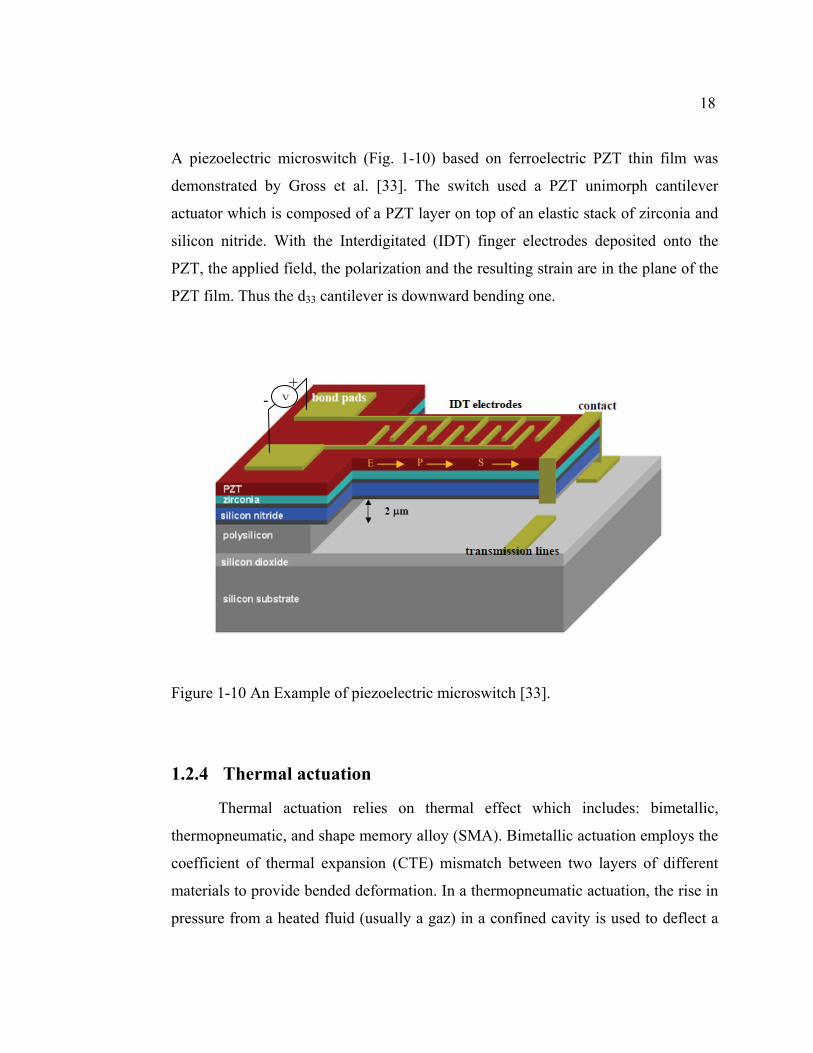
A piezoelectric microswitch (Fig. 1-10) based on ferroelectric PZT thin film was
demonstrated by Gross et al. [33]. The switch used a PZT unimorph cantilever
actuator which is composed of a PZT layer on top of an elastic stack of zirconia and
silicon nitride. With the Interdigitated (IDT) finger electrodes deposited onto the
PZT, the applied field, the polarization and the resulting strain are in the plane of the
PZT film. Thus the d33 cantilever is downward bending one.
Figure 1-10 An Example of piezoelectric microswitch [33].
1.2.4 Thermal actuation
Thermal actuation relies on thermal effect which includes: bimetallic,
thermopneumatic, and shape memory alloy (SMA). Bimetallic actuation employs the
coefficient of thermal expansion (CTE) mismatch between two layers of different
materials to provide bended deformation. In a thermopneumatic actuation, the rise in
pressure from a heated fluid (usually a gaz) in a confined cavity is used to deflect a
V
E P S
+ -
19
membrane [34]. Thermo pneumatic actuation is a slow technique but offers very high
forces.
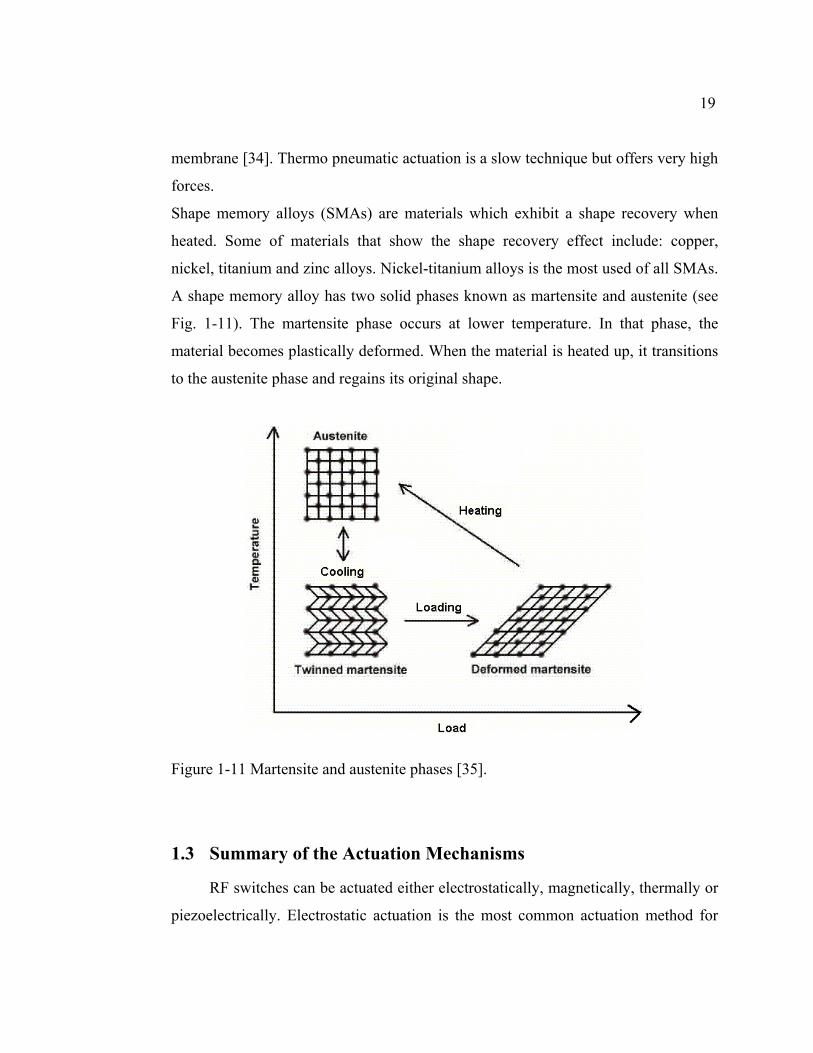
Shape memory alloys (SMAs) are materials which exhibit a shape recovery when
heated. Some of materials that show the shape recovery effect include: copper,
nickel, titanium and zinc alloys. Nickel-titanium alloys is the most used of all SMAs.
A shape memory alloy has two solid phases known as martensite and austenite (see
Fig. 1-11). The martensite phase occurs at lower temperature. In that phase, the
material becomes plastically deformed. When the material is heated up, it transitions
to the austenite phase and regains its original shape.
Figure 1-11 Martensite and austenite phases [35].
1.3 Summary of the Actuation Mechanisms
RF switches can be actuated either electrostatically, magnetically, thermally or
piezoelectrically. Electrostatic actuation is the most common actuation method for
20
the advantages of low power consumption and ease of integration with a wide variety
of fabrication processes, but it may require high voltages to achieve high forces and
deflections. Similarly, piezoelectric actuation can offer very high forces but very
small deflections with very large voltages. Magnetic actuation is able to provide
large forces that produce large deflections, however it is power inefficient. In the
case of thermal actuation, the forces are relatively large, but it does tend to increase
the switching time and induce noise voltages because of thermal voltage generation
effects.
1.4 Discussion about Power Handling and Linearity Capabilities
Power handling capability is an important parameter of an RF switch. It
indicates that the switch can transmit the power without degradation. Often, power
handling and linearity are related; for example the power handling ability for MEMS
switch can be limited by the current density causing excessive heat in the circuit,
which lead to passive intermodulation product (PIM), a nonlinear effect that will be
presented in the next sub-section.
1.4. 1 Low and high power switches
In the previous sections, semiconductor (PIN diode - GaAsFET) and MEMS
switches have been studied. These devices have power limitations arising from
materials properties and/or device design; this prevents them from being used in
high-power applications such as in transmitters in satellite and radars. For instance,
PIN diode needs large bias current and long switch settling time for high power
operation [36]-[37]. GaAsFET transistors suffer from low power capability due to
nature of the material [38]. Moreover, MEMS switches have low power handling
capability (< 1W). Conversely, switches such as Ferrite waveguide switches are
popular for high power applications. Switching is realized by applying magnetic field
to change the permeability of the ferromagnetic material. However, they have large
21
size and mass. Also more energy is required to have the switching magnetic field.
Another high power switch is the mechanical switch (e.g. coaxial switch, waveguide
switch), which performs switching by moving some metal parts in the waveguide.
Mechanical switches can have higher power handling capability as their sizes
increase. However, they are unreliable for prolongation applications (e.g. metal parts
wear out over time).
1.4.2 Nonlinearity problem
In high power RF/microwave systems (e.g. satellite system), passive
components such as connectors, switches, cables and antennas are normally
considered linear. They can however exhibit nonlinear behaviour when they are
subjected to sufficient high power input signals. This nonlinearity generates unwanted signals (interference) at the output, creating harmonics and in-band
intermodulation products. This phenomena is called passive intermodulation (PIM)
and it appears at frequencies [39]:
M
0 i ii 1
f m f 1.7=
=∑
Where mi are integers and M is the number of the input frequencies. The sum M
ii 1m
=∑ defines the order of the intermodulation product. In the case of two input
frequencies f1 and f2 (see Fig. 1-12) equation (1.7) becomes:
0 1 1 2 2 1 2 2 1 1 2 2
1 1 2 2 1 1 2
f m f m f f f 2f f 2f f 3f2f 3f 2f 4f 3f 4f 3f ............. 1.8
= + = + + − + − +− + − + − + − +
22
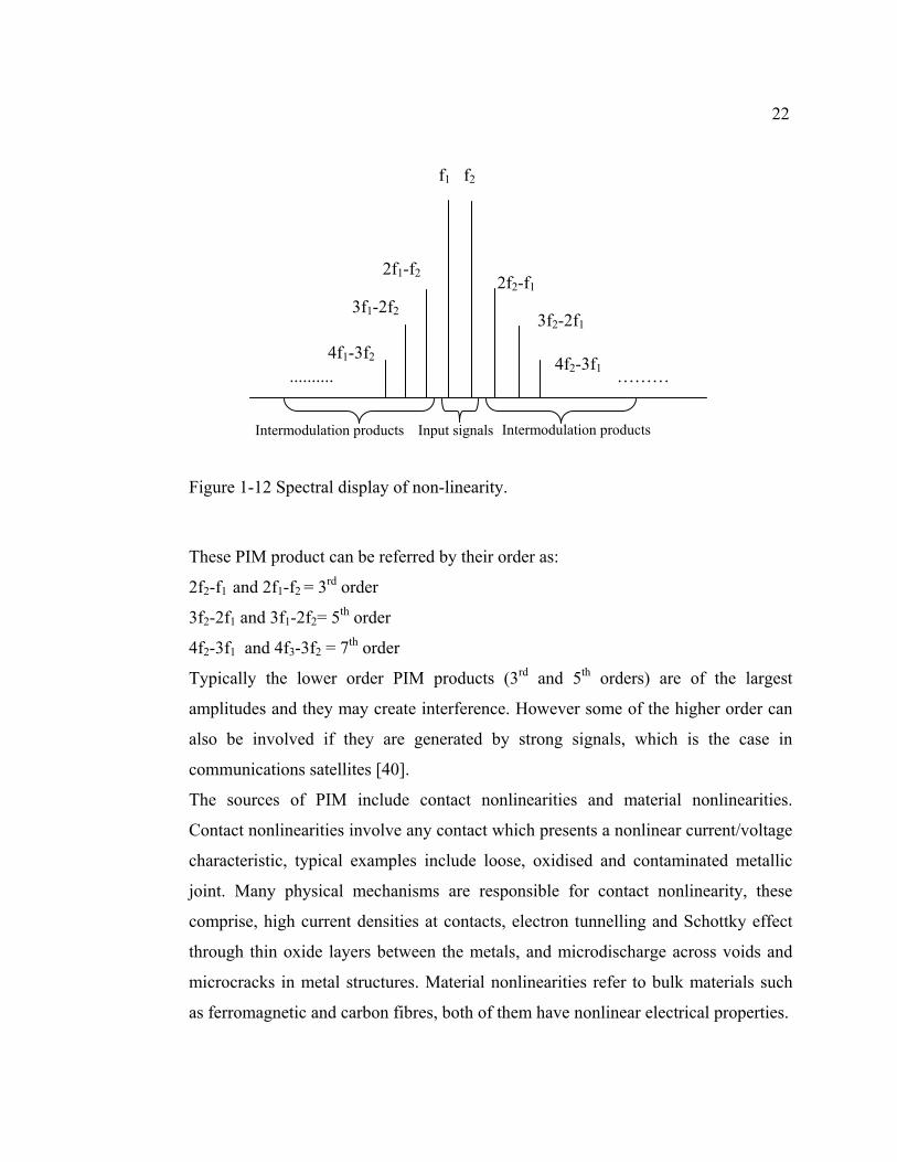
Figure 1-12 Spectral display of non-linearity.
These PIM product can be referred by their order as:
2f2-f1 and 2f1-f2 = 3rd order
3f2-2f1 and 3f1-2f2= 5th order
4f2-3f1 and 4f3-3f2 = 7th order
Typically the lower order PIM products (3rd and 5th orders) are of the largest
amplitudes and they may create interference. However some of the higher order can
also be involved if they are generated by strong signals, which is the case in
communications satellites [40].
The sources of PIM include contact nonlinearities and material nonlinearities.
Contact nonlinearities involve any contact which presents a nonlinear current/voltage
characteristic, typical examples include loose, oxidised and contaminated metallic
joint. Many physical mechanisms are responsible for contact nonlinearity, these
comprise, high current densities at contacts, electron tunnelling and Schottky effect
through thin oxide layers between the metals, and microdischarge across voids and
microcracks in metal structures. Material nonlinearities refer to bulk materials such
as ferromagnetic and carbon fibres, both of them have nonlinear electrical properties.
f1 f2
2f1-f2
Intermodulation products
4f2-3f1
3f2-2f1
2f2-f1
Input signals
………
Intermodulation products
..........
3f1-2f2
4f1-3f2
23
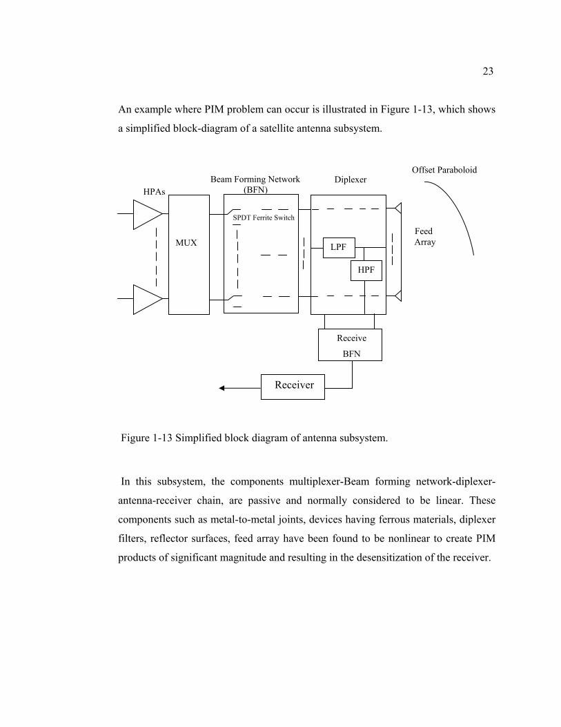
An example where PIM problem can occur is illustrated in Figure 1-13, which shows
a simplified block-diagram of a satellite antenna subsystem.
Figure 1-13 Simplified block diagram of antenna subsystem.
In this subsystem, the components multiplexer-Beam forming network-diplexer-
antenna-receiver chain, are passive and normally considered to be linear. These
components such as metal-to-metal joints, devices having ferrous materials, diplexer
filters, reflector surfaces, feed array have been found to be nonlinear to create PIM
products of significant magnitude and resulting in the desensitization of the receiver.
Feed Array
Receive
BFN
Receiver
Diplexer
HPF
HPAs Beam Forming Network
(BFN)
SPDT Ferrite Switch
Offset Paraboloid
LPF
MUX
24
CHAPTER 2. RF SWITCHES USING A POLYIMIDE
MEMBRANE
2.1 Introduction As mentioned in the previous chapter, semi-conductors and MEMS switching
elements have significant RF performance limitations either at high frequencies or at
high power levels. RF MEMS have high isolation, low insertion loss, extreme
linearity at frequencies (10-100 GHz) for RF power levels less than 1W. Semi-
conductor devices introduce distortions in the input signal at high frequencies (above
1 GHz) and cannot handle high RF power. On the other hand, mechanical switches
(coaxial and waveguide) perform well at high frequencies but are power inefficient,
bulky and heavy. Furthermore, ferrite latching switches offer low power
consumption and good performance at high power, nonetheless, they are heavy. In
satellite systems with stringent requirements of size, mass, cost, power handling and
power consumption these components require a new solution. Here, we propose
novel RF latching switching elements. They may offer potential substitute for the
aforementioned devices in space applications. The switches are built from thin
polyimide membrane and operate with low currents remaining in steady states with
zero DC power consumption. They offer negligible loss and have no bias lines in the
propagation media. In addition, their materials are passive and may demonstrate
linear behavior at high power levels.
The switches are intended to be implemented in open and closed waveguides.
The design aspect is described in section 2.2, the material choice is given in section
2.3, the principle of operation is presented in section 2.4, the mechanical aspect is
discussed in section 2.5, the magnetic aspect is considered in section 2.6, the
calculated magnetic field is presented in section 2.7, the experimental validation is
shown in section 2.8, then the conclusion is stated in section 2.9.
25
2.2 Switches Design
We designed and fabricated two types of waveguide switches. Type 1 is
intended to be implemented in a waveguide antenna (Fig. 2.1) while type 2 is meant
to be incorporated into a closed waveguide (Fig. 2.2). The switches have a cantilever
beam made of Kapton® polyimide substrate (metalized at one side) as the base
material. They have fixed and movable beams. For type 1 switch, the movable beam
comprises a periodic array of narrow metalized strips printed on the polyimide layer
(dielectric). These flexible strips are making a mechanical connection between the
rigid part of the movable beam consisting of a magnetic material plate bonded to the
base material, and the fixed beam which is also made of metalized polyimide. The
copper strips are formed to prevent the unwanted warpage resulting from the stress of
switching and to conduct RF current in the OFF state (from the bottom to the top of
the waveguide). For type 2 switch, the movable beam however, consists of a first
section (flexible beam) of non-metalized polyimide substrate and second section
(rigid beam) in which a magnetic plate is bonded to the polyimide substrate. The
magnetic plate is responsible for actuating the switch. While the non-metalized
substrate is responsible for connecting the fixed and rigid beams and making an easy
bending.
26
(a)
(b)
Figure 2-1 Schematic representation of the type 1 switch in the ON state. (a)
Perspective view, (b) Top view.
W = 800 mils
L = 270 mils
l = 150 mils
T = 4.8 mils
t = 2.38 mils
27
(a)
(b)
Figure 2-2 Schematic representation of the type 2 switch in the ON state. (a)
Perspective view, (b) Top view.
Legend:
W: Width of the movable beam
l : Length of the flexible beam
W = 400 mils
L = 400 mils
l = 200 mils
T = 4.8 mils
t = 2.38 mils
28
L : Length of the rigid beam
T : Thickness of the magnetic plate
t : Thickness of the base material (polyimide sheet : 1 mil + copper layers : 35
microns)
2.3 Material Choice
One concern behind this project was to use as low magnetic field (low drive
current) as possible to actuate the switches. For this reason, the material for the
switches has to be chosen very carefully. A base material should be flexible, thin,
and strong enough to resist the bending stress generated by the switch while a
magnetic material needs to have a high permeability. A Single-Sided Copper-Clad
polyimide (Dupont) [41] having 35 microns copper layers deposited on a 1 mil
(25.4 microns) thick Kapton® sheet was preferred due to the low thickness of the
polyimide. Thin films of high-permeability and low remanence material (Metglas
2826MB1 of company Metglas®) [42]) have been chosen, as a magnetic material. It
offers a very high permeability (µr > 50 000) which allows high magnetization in a
relatively low applied magnetic field.
Prototype switches of different polyimide thicknesses were tested for
actuation. With a very thin substrate (0.5 mil), the switch was unstable when
subjected to external disturbances. With a greater thickness (2 mils), the switch is
less sensitive to disturbances but requires more actuation current.
2.4 Principle of Operation
Figures 2-3(a) and (b) show schematically a type 1 switch implemented in an
open waveguide (waveguide antenna) and type 2 switch implemented in a closed
waveguide respectively. Both waveguides are non-standard WR90 of dimensions
900x80 mils2. The 80 mils height was chosen to have low (DC currents) magnetic
fields to actuate the switches. A permanent magnet is bonded to the top broad wall of
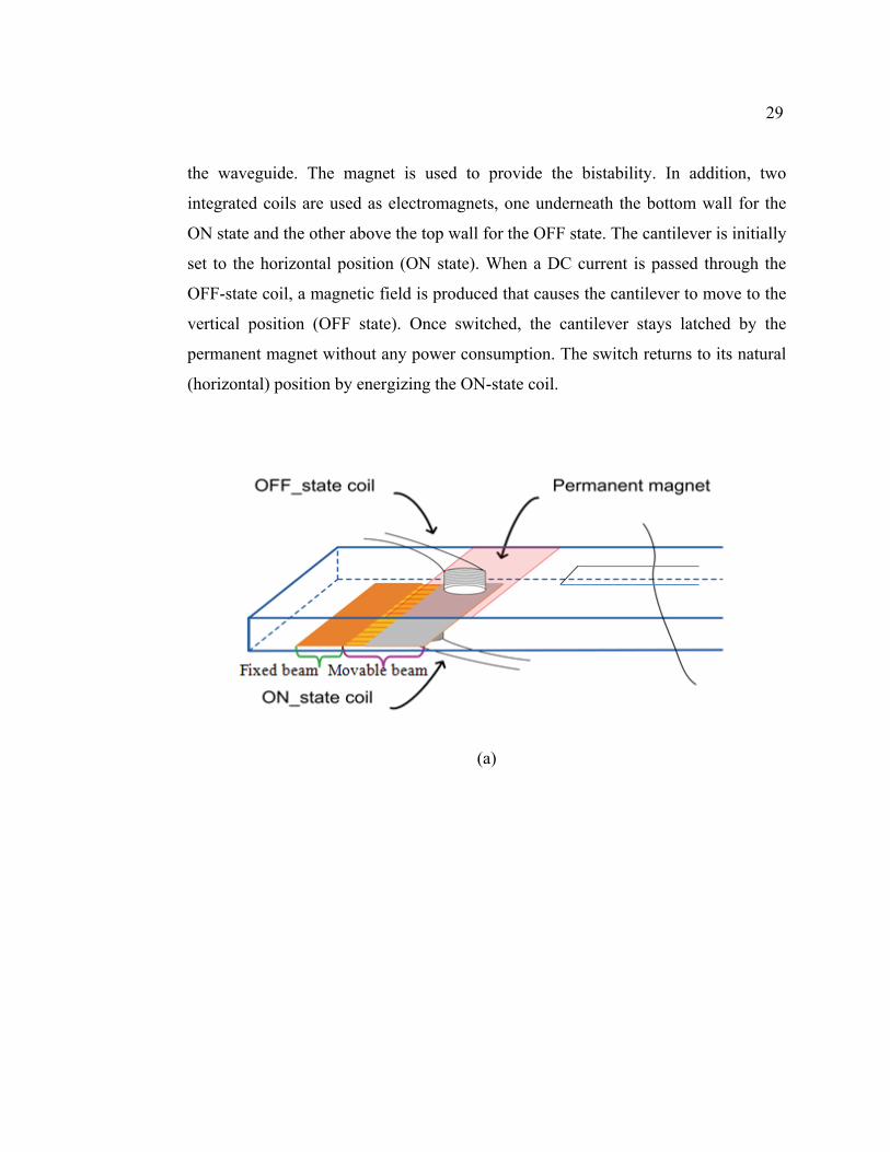
29
the waveguide. The magnet is used to provide the bistability. In addition, two
integrated coils are used as electromagnets, one underneath the bottom wall for the
ON state and the other above the top wall for the OFF state. The cantilever is initially
set to the horizontal position (ON state). When a DC current is passed through the
OFF-state coil, a magnetic field is produced that causes the cantilever to move to the
vertical position (OFF state). Once switched, the cantilever stays latched by the
permanent magnet without any power consumption. The switch returns to its natural
(horizontal) position by energizing the ON-state coil.
(a)
30
(b)
Figure 2-3 Schematic illustration of the integration of the switches into the
waveguides along with the switching and bistability mechanisms. Switches are
shown in the ON states, (a) type 1 switch in a waveguide antenna (b) type 2 switch in
a closed waveguide.
2.5 Mechanical Analysis
In Fig. 2-4, a plate of magnetic material of length L is bonded on a flexible
dielectric substrate. It is assumed that the structure is in the vicinity of a magnet
(permanent or electromagnet). Initially, if the cantilever is in the horizontal position
( 0θ = in the figure) and the applied H field is vertical and uniform as illustrated, the
magnetization in the material will be predominantly vertical. In practice, however the
applied H field is never perfectly uniform and it can be assumed that it will have
some horizontal component. Given the large length/thickness ratio of the plate, it will
have a much stronger demagnetization factor for normal field than for tangential
field. Consequently, it can be assumed that a magnetization vector M will develop
along the L dimension of the plate even if the horizontal component of the applied H
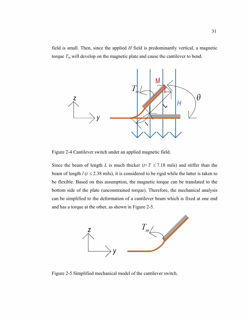
31
field is small. Then, since the applied H field is predominantly vertical, a magnetic
torque Tm will develop on the magnetic plate and cause the cantilever to bend.
Figure 2-4 Cantilever switch under an applied magnetic field.
Since the beam of length L is much thicker (t+T ≤ 7.18 mils) and stiffer than the
beam of length l (t ≤ 2.38 mils), it is considered to be rigid while the latter is taken to
be flexible. Based on this assumption, the magnetic torque can be translated to the
bottom side of the plate (unconstrained torque). Therefore, the mechanical analysis
can be simplified to the deformation of a cantilever beam which is fixed at one end
and has a torque at the other, as shown in Figure 2-5.
Figure 2-5 Simplified mechanical model of the cantilever switch.

32
The application of a torque causes a deflection of the cantilever beam along an arc of
circle with radius of curvature R that is determined by [43]. (see Fig. 2-6).
Figure 2-6 Schematic illustration of the cantilever switch under an applied torque.
2.1m
EIRT
=
Where E, I are the Young’s modulus, the surface moment of inertia of the flexible
beam respectively.
The angular mechanical deflection can be expressed as:
2.2l
Rθ =
With l is the length of the flexible beam.
Its relationship with the applied torque Tm is given by:
2 .3ml T
EIθ =
The moment of inertia I depends on the cross section of flexible beam. The latter has
a rectangular cross section (see Figure 2-7). For the flexible beam of the type 1
switch, the copper metallization is thicker than the polyimide layer and it has a much
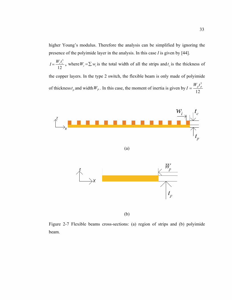
33
higher Young’s modulus. Therefore the analysis can be simplified by ignoring the
presence of the polyimide layer in the analysis. In this case I is given by [44]. 3
12c cW tI = , where c iW w=∑ is the total width of all the strips and ct is the thickness of
the copper layers. In the type 2 switch, the flexible beam is only made of polyimide
of thickness pt and width PW . In this case, the moment of inertia is given by3
12p pW t
I =
(a)
(b)
Figure 2-7 Flexible beams cross-sections: (a) region of strips and (b) polyimide
beam.
34
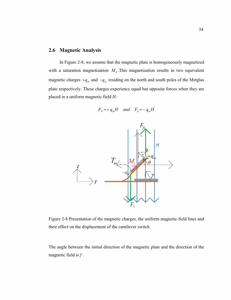
2.6 Magnetic Analysis
In Figure 2-8, we assume that the magnetic plate is homogeneously magnetized
with a saturation magnetization SM .This magnetization results in two equivalent
magnetic charges mq+ and mq− residing on the north and south poles of the Metglas
plate respectively. These charges experience equal but opposite forces when they are
placed in a uniform magnetic field H:
N m S mF q H and F q H=+ = −
Figure 2-8 Presentation of the magnetic charges, the uniform magnetic field lines and
their effect on the displacement of the cantilever switch.
The angle between the initial direction of the magnetic plate and the direction of the
magnetic field isγ .

35
Due to the applied torque, the magnetic plate is oriented at an angle θ. The forces NF and SF generate a torque that can be expressed as:
sin ( ) sin ( ) sin ( )m m S ST q HL M WTLH M V Hγ θ γ θ γ θ= − = − = −
Where V and SM are the volume and saturation magnetization of the metglas plate
respectively.
We will assume that the magnetic field is held constant ( 90 )γ = ° . This leads to
sin (90 ) cos 2.4m S ST M V H M V Hθ θ= − = This expression indicates that as the deflection angle increases the torque decreases
and eventually an equilibrium is reached between the applied magnetic torque and
the deflection resistance of the flexible beam.
2.7 Magnetic Field Density Calculation
Equating eq. 2.3 and 2.4 yields the relationship between H and θ
/ 2.5cosS
EIH A mM lV
θθ
=
The magnetic flux density can be written as :
0 0 2.6cosS
EIB H TeslaM lV
θθ
=μ =μ
For type 1 switch, Eq. 2.6 can be written as: 3
0 2.712 cos
c c
S
EW tBM lV
θθ
=μ

36
For type 2 switch, it can be expressed as: 3
0 2.812 cos
p p
S
EW tB
M lVθ
θ=μ
The angular deflection θ can be determined by solving the following equation
obtained by simple geometrical analysis from Figure 2.6.
sin (1 cos ) 2.9ld L θ θθ
= + −
Where d, l, L are maximal tip deflection, length of the flexible beam and length of
the rigid beam respectively.
Based on equation 2.7 for type 1 switch, and using the numerical values in Table 2.1,
the minimum flux density necessary to move the tip of the cantilever from the bottom
wall to the top wall of the 80 mils thick waveguide is 12.6 mT.
Table 2.1 Parameters used to calculate the magnetic flux density.
Parameters Dimensions
L: Length of the magnetic plate 270 mils
W: Width of the magnetic plate 800 mils
T: Thickness of the magnetic plate 4.8 mils
cW : Total width of the copper strips 224 mils
l: Length of the copper strips (flexible beam) 150 mils
ct : Thickness of the copper strips (flexible beam) 1.38 mil (35μm)
SM : Saturation magnetization of the Metglas 0.88 tesla [42]
E: Young’s modulus of copper strips 117 GPas [45]
d: Maximal tip deflection 80 mils (2 mm)
θ: Angular deflection for contact 0.234 rad
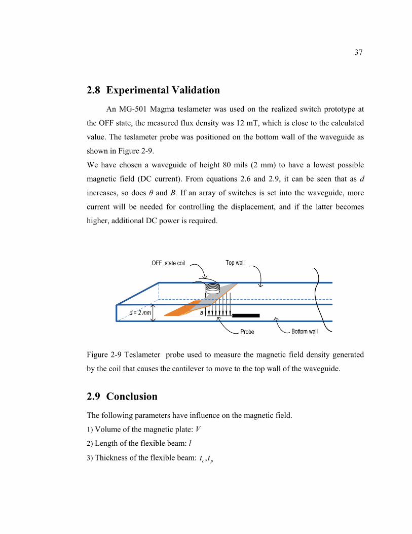
37
2.8 Experimental Validation
An MG-501 Magma teslameter was used on the realized switch prototype at
the OFF state, the measured flux density was 12 mT, which is close to the calculated
value. The teslameter probe was positioned on the bottom wall of the waveguide as
shown in Figure 2-9.
We have chosen a waveguide of height 80 mils (2 mm) to have a lowest possible
magnetic field (DC current). From equations 2.6 and 2.9, it can be seen that as d
increases, so does θ and B. If an array of switches is set into the waveguide, more
current will be needed for controlling the displacement, and if the latter becomes
higher, additional DC power is required.
Figure 2-9 Teslameter probe used to measure the magnetic field density generated
by the coil that causes the cantilever to move to the top wall of the waveguide.
2.9 Conclusion
The following parameters have influence on the magnetic field.
1) Volume of the magnetic plate: V
2) Length of the flexible beam: l
3) Thickness of the flexible beam: ,c pt t
38
4) Width of the flexible beam: ,p cW W
The volume of the magnetic plate highly influences the amount of the necessary
magnetic field because 1V
Β∝ , as seen in eq. 2.6. Hence, the practical way to lower
the field is to increase the volume. This is not true if gravitational force is taken into
account. If V is increased, an additional weight will have to be lifted and B will
increase. Furthermore, the thickness t of the base material (copper or polyimide) is
very crucial as B is proportional to I (3
12WtB I∝ = ). So, for a lower magnetic field
density, it is important that the cantilever is fabricated as thin as possible.
39
CHAPTER 3. LEAKY WAVE ANTENNA USING A
MEMBRANE SWITCH
3.1 Introduction An antenna that is capable to alter its radiation characteristics, such as
operating frequency, polarization or radiation pattern is referred to as a
reconfigurable antenna. It provides a unique way to serve different functionalities at
different frequency bands, which may lead to considerable saving in size, weight and
cost. The reconfiguration can be achieved through switches and variable capacitors.
In some design [46]-[47] MEMS switches or PIN diodes are used to change the
length of an antenna element such as dipole or a slot, thereby shifting the frequency
of operation (resonant frequency). Other approaches make use of varactors to steer or
tune the beam of an antenna [48].
The work described here deals with the design, implementation and
measurement of a leaky wave antenna in which a membrane switch is incorporated.
Strictly speaking, the capability to switch the antenna between ON and OFF states
cannot be considered as reconfigurability. However, by incorporating an array of
switches in a beam forming network it becomes possible to reconfigure the radiation
pattern. Consequently, the switch presented in this chapter should be considered as a
building block enabling the synthesis of reconfigurable antennas.
3.2 Leaky Waveguide Antenna Theory
A longitudinal slot cut into the broad wall of a rectangular waveguide is known
as one of the leaky waveguide antennas. A wave traveling along the waveguide leaks
(or radiates) energy as it propagates. The angle at which the leakage occurs is given
by:
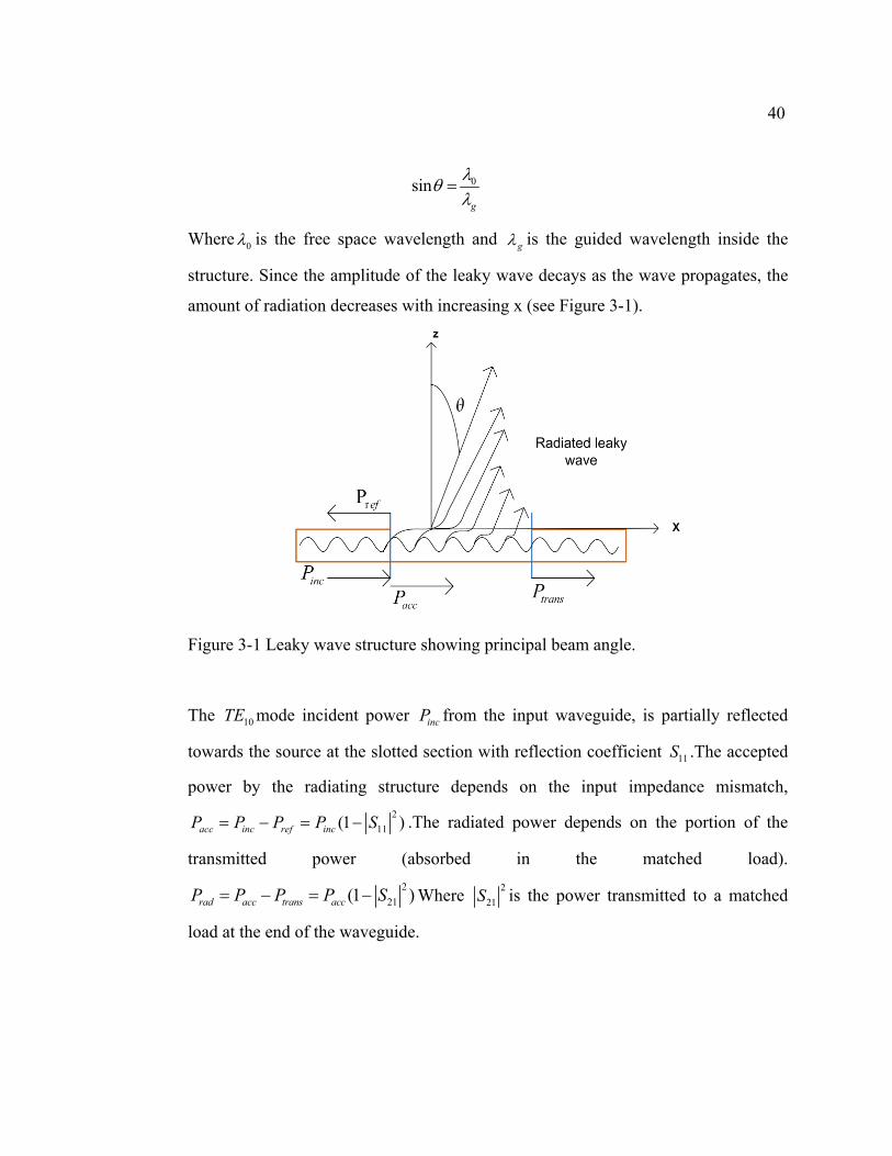
40
0sing
λθλ
=
Where 0λ is the free space wavelength and gλ is the guided wavelength inside the
structure. Since the amplitude of the leaky wave decays as the wave propagates, the
amount of radiation decreases with increasing x (see Figure 3-1).
Figure 3-1 Leaky wave structure showing principal beam angle.
The 10TE mode incident power incP from the input waveguide, is partially reflected
towards the source at the slotted section with reflection coefficient 11S .The accepted
power by the radiating structure depends on the input impedance mismatch, 2
11(1 )acc inc ref incP P P P S= − = − .The radiated power depends on the portion of the
transmitted power (absorbed in the matched load). 2
21(1 )rad acc trans accP P P P S= − = − Where 221S is the power transmitted to a matched
load at the end of the waveguide.
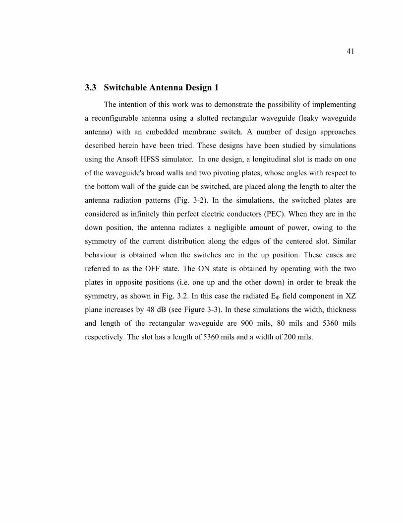
41
3.3 Switchable Antenna Design 1
The intention of this work was to demonstrate the possibility of implementing
a reconfigurable antenna using a slotted rectangular waveguide (leaky waveguide
antenna) with an embedded membrane switch. A number of design approaches
described herein have been tried. These designs have been studied by simulations
using the Ansoft HFSS simulator. In one design, a longitudinal slot is made on one
of the waveguide's broad walls and two pivoting plates, whose angles with respect to
the bottom wall of the guide can be switched, are placed along the length to alter the
antenna radiation patterns (Fig. 3-2). In the simulations, the switched plates are
considered as infinitely thin perfect electric conductors (PEC). When they are in the
down position, the antenna radiates a negligible amount of power, owing to the
symmetry of the current distribution along the edges of the centered slot. Similar
behaviour is obtained when the switches are in the up position. These cases are
referred to as the OFF state. The ON state is obtained by operating with the two
plates in opposite positions (i.e. one up and the other down) in order to break the
symmetry, as shown in Fig. 3.2. In this case the radiated EΦ field component in XZ
plane increases by 48 dB (see Figure 3-3). In these simulations the width, thickness
and length of the rectangular waveguide are 900 mils, 80 mils and 5360 mils
respectively. The slot has a length of 5360 mils and a width of 200 mils.
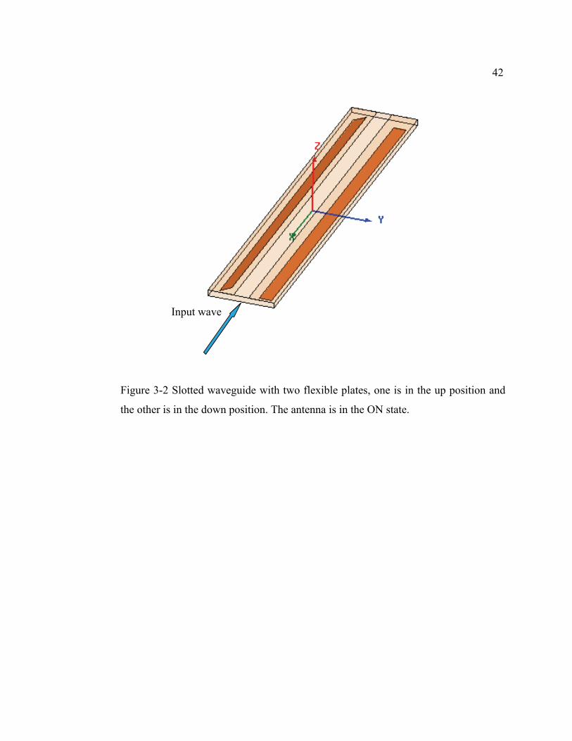
42
Figure 3-2 Slotted waveguide with two flexible plates, one is in the up position and
the other is in the down position. The antenna is in the ON state.
Input wave
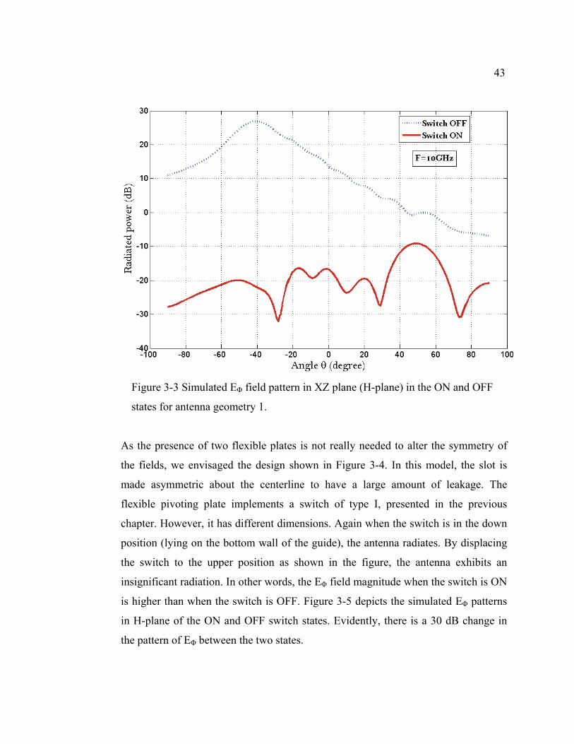
43
Figure 3-3 Simulated EΦ field pattern in XZ plane (H-plane) in the ON and OFF
states for antenna geometry 1.
As the presence of two flexible plates is not really needed to alter the symmetry of
the fields, we envisaged the design shown in Figure 3-4. In this model, the slot is
made asymmetric about the centerline to have a large amount of leakage. The
flexible pivoting plate implements a switch of type I, presented in the previous
chapter. However, it has different dimensions. Again when the switch is in the down
position (lying on the bottom wall of the guide), the antenna radiates. By displacing
the switch to the upper position as shown in the figure, the antenna exhibits an
insignificant radiation. In other words, the EΦ field magnitude when the switch is ON
is higher than when the switch is OFF. Figure 3-5 depicts the simulated EΦ patterns
in H-plane of the ON and OFF switch states. Evidently, there is a 30 dB change in
the pattern of EΦ between the two states.
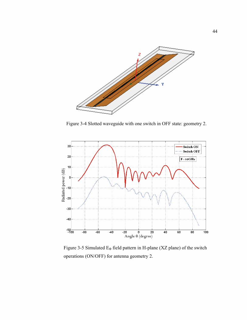
44
Figure 3-4 Slotted waveguide with one switch in OFF state: geometry 2.
Figure 3-5 Simulated EΦ field pattern in H-plane (XZ plane) of the switch
operations (ON/OFF) for antenna geometry 2.

45
A prototype switch of small size was tested for actuation as well as to
investigate the energy needed to control the antenna. Experiments show a switching
current of 43 mA and 150 mA for moving the plate up and down respectively. Once
the device is in the up position, it has been observed that the upper edge of the
flexible membrane does not make a uniform physical contact with the broad wall.
This allows more radiated power in the OFF state, which is not a desired behaviour.
Therefore, it would not be practical to implement an antenna with a long switch or an
array of switches. To that end, this design approach was not pursued, and was
replaced by the one described below.
3.4 Switchable Antenna Design 2
The proposed antenna consists of a (900x80x9760) mils3 slotted rectangular
waveguide and uses the membrane type I switch presented in chapter 2 (see Fig. 3-6).
The fixed and movable plates implementing the switch are modeled as PEC plates
with zero thickness. The switch is placed 540 mils away from the waveguide input
port (before the slot) and 50 mils from the waveguide sidewalls. The 800x150 mils2
movable part is composed of thin conducting strips which are spaced apart from one
another by air gaps of size s = 45 mils. There are 14 strips, and each strip is of width
w = 15 mils.
The slot (Fig. 3-7) is 6760 mils long, 200 mils wide and is asymmetric about
the center line. The asymmetry provides a single narrow beam whereas the chosen
length and width allow a high gain. It is etched from the copper cladding on the
upper side of the waveguide (broad wall). The latter is made of 10 mils RT/duroid
6002 material with a relative dielectric constant of 2.94 and a loss tangent of 0.0012.
In order to fasten the broad wall to the waveguide, two screwed metal bars are
incorporated into the design. For this aim, the upper side has to be wider (1500 mils)
than the waveguide (900 mils) as it can be seen from Figures 3-6 and 3-7.
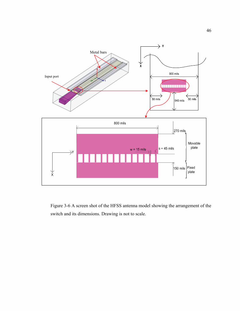
46
Figure 3-6 A screen shot of the HFSS antenna model showing the arrangement of the
switch and its dimensions. Drawing is not to scale.
Metal bars
Input port
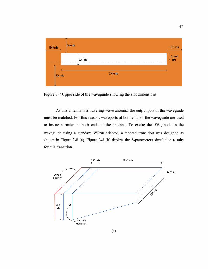
47
Figure 3-7 Upper side of the waveguide showing the slot dimensions.
As this antenna is a traveling-wave antenna, the output port of the waveguide
must be matched. For this reason, waveports at both ends of the waveguide are used
to insure a match at both ends of the antenna. To excite the 10TE mode in the
waveguide using a standard WR90 adaptor, a tapered transition was designed as
shown in Figure 3-8 (a). Figure 3-8 (b) depicts the S-parameters simulation results
for this transition.
(a)
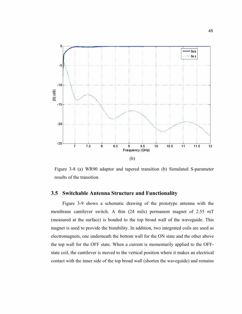
48
(b)
Figure 3-8 (a) WR90 adaptor and tapered transition (b) Simulated S-parameter
results of the transition.
3.5 Switchable Antenna Structure and Functionality
Figure 3-9 shows a schematic drawing of the prototype antenna with the
membrane cantilever switch. A thin (24 mils) permanent magnet of 2.55 mT
(measured at the surface) is bonded to the top broad wall of the waveguide. This
magnet is used to provide the bistability. In addition, two integrated coils are used as
electromagnets, one underneath the bottom wall for the ON state and the other above
the top wall for the OFF state. When a current is momentarily applied to the OFF-
state coil, the cantilever is moved to the vertical position where it makes an electrical
contact with the inner side of the top broad wall (shorten the waveguide) and remains
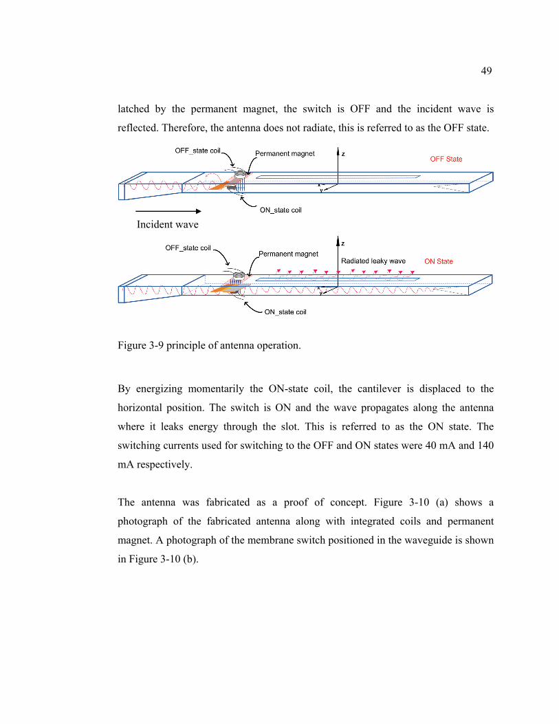
49
latched by the permanent magnet, the switch is OFF and the incident wave is
reflected. Therefore, the antenna does not radiate, this is referred to as the OFF state.
Figure 3-9 principle of antenna operation.
By energizing momentarily the ON-state coil, the cantilever is displaced to the
horizontal position. The switch is ON and the wave propagates along the antenna
where it leaks energy through the slot. This is referred to as the ON state. The
switching currents used for switching to the OFF and ON states were 40 mA and 140
mA respectively.
The antenna was fabricated as a proof of concept. Figure 3-10 (a) shows a
photograph of the fabricated antenna along with integrated coils and permanent
magnet. A photograph of the membrane switch positioned in the waveguide is shown
in Figure 3-10 (b).
Incident wave
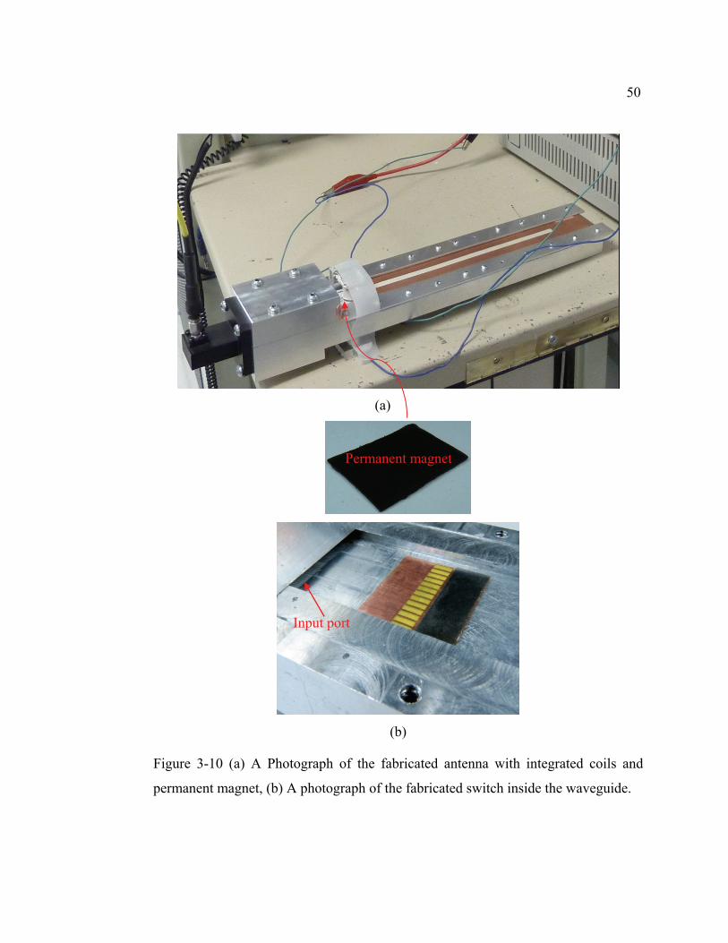
50
(a)
(b)
Figure 3-10 (a) A Photograph of the fabricated antenna with integrated coils and
permanent magnet, (b) A photograph of the fabricated switch inside the waveguide.
Permanent magnet
Input port
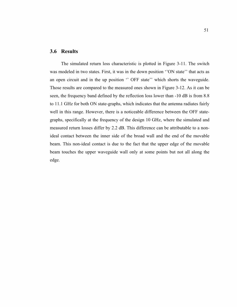
51
3.6 Results
The simulated return loss characteristic is plotted in Figure 3-11. The switch
was modeled in two states. First, it was in the down position ‘’ON state’’ that acts as
an open circuit and in the up position ‘’ OFF state’’ which shorts the waveguide.
Those results are compared to the measured ones shown in Figure 3-12. As it can be
seen, the frequency band defined by the reflection loss lower than -10 dB is from 8.8
to 11.1 GHz for both ON state-graphs, which indicates that the antenna radiates fairly
well in this range. However, there is a noticeable difference between the OFF state-
graphs, specifically at the frequency of the design 10 GHz, where the simulated and
measured return losses differ by 2.2 dB. This difference can be attributable to a non-
ideal contact between the inner side of the broad wall and the end of the movable
beam. This non-ideal contact is due to the fact that the upper edge of the movable
beam touches the upper waveguide wall only at some points but not all along the
edge.
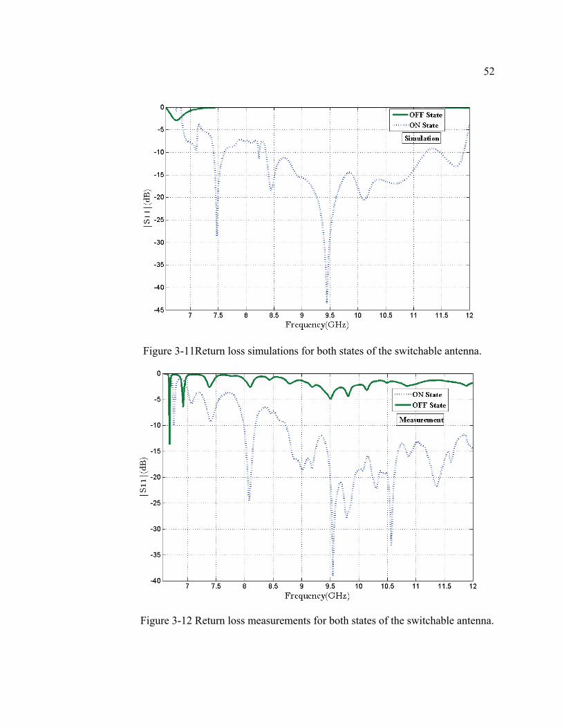
52
Figure 3-11Return loss simulations for both states of the switchable antenna.
Figure 3-12 Return loss measurements for both states of the switchable antenna.
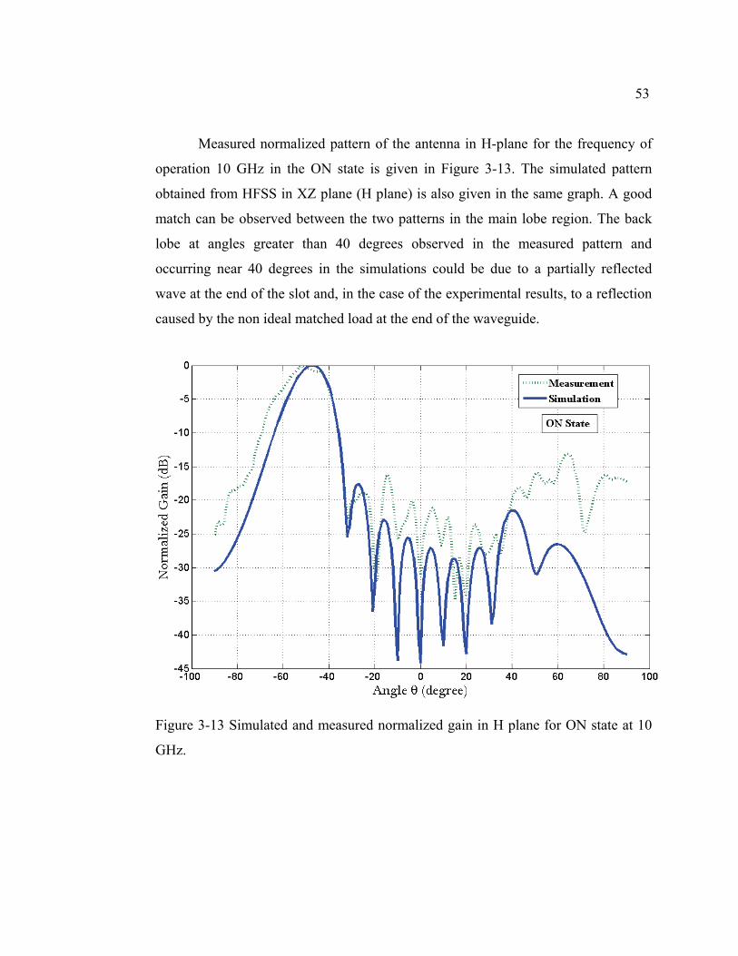
53
Measured normalized pattern of the antenna in H-plane for the frequency of
operation 10 GHz in the ON state is given in Figure 3-13. The simulated pattern
obtained from HFSS in XZ plane (H plane) is also given in the same graph. A good
match can be observed between the two patterns in the main lobe region. The back
lobe at angles greater than 40 degrees observed in the measured pattern and
occurring near 40 degrees in the simulations could be due to a partially reflected
wave at the end of the slot and, in the case of the experimental results, to a reflection
caused by the non ideal matched load at the end of the waveguide.
Figure 3-13 Simulated and measured normalized gain in H plane for ON state at 10
GHz.
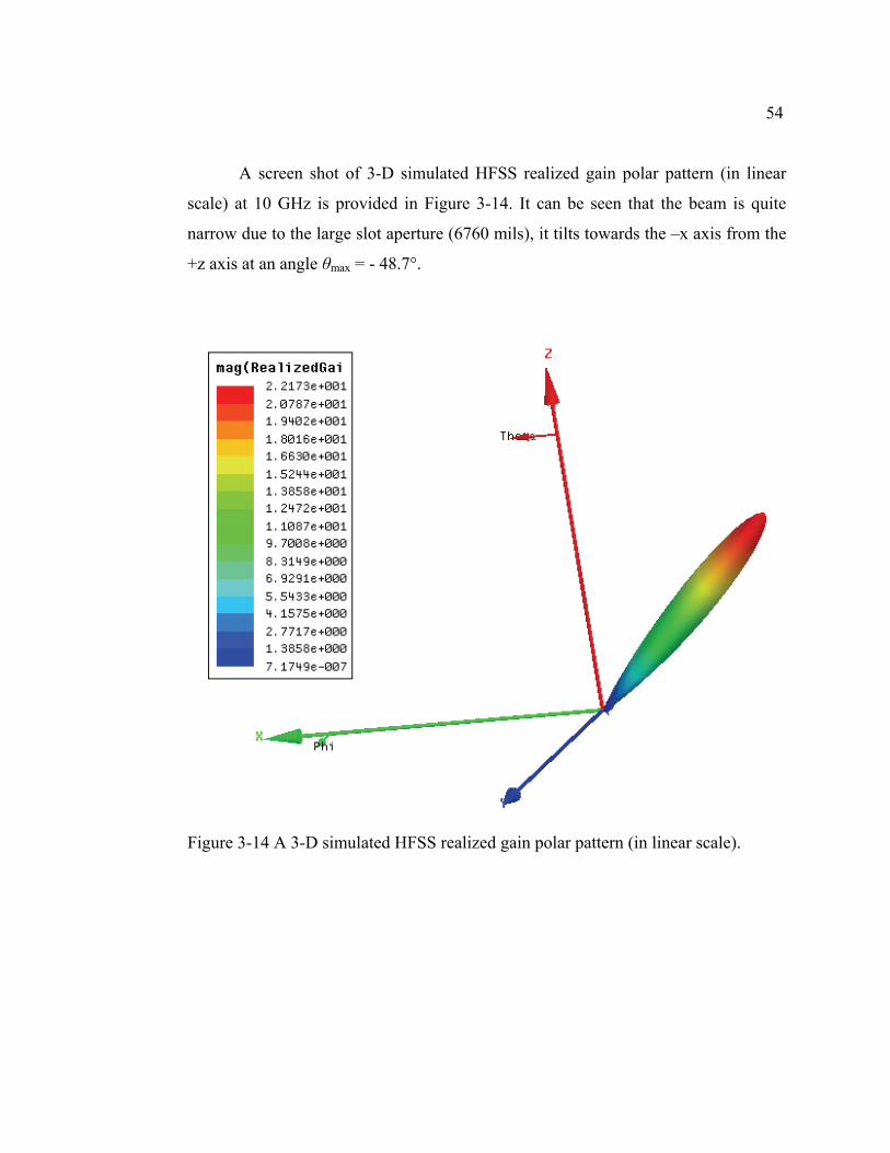
54
A screen shot of 3-D simulated HFSS realized gain polar pattern (in linear
scale) at 10 GHz is provided in Figure 3-14. It can be seen that the beam is quite
narrow due to the large slot aperture (6760 mils), it tilts towards the –x axis from the
+z axis at an angle θmax = - 48.7°.
Figure 3-14 A 3-D simulated HFSS realized gain polar pattern (in linear scale).
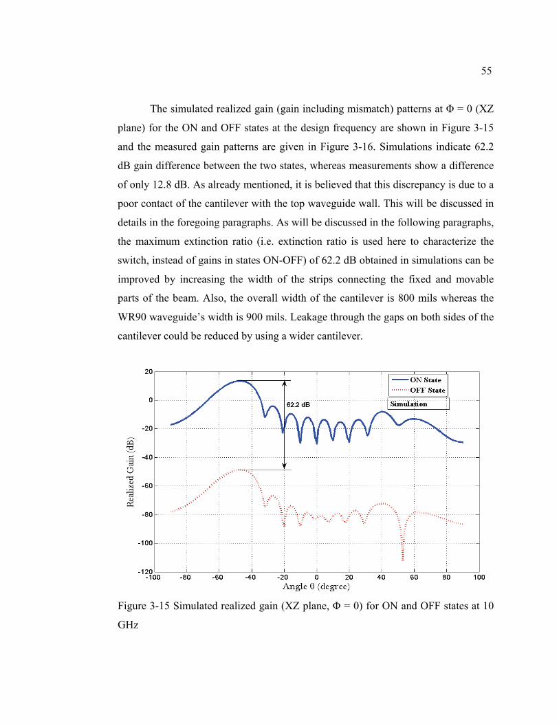
55
The simulated realized gain (gain including mismatch) patterns at Φ = 0 (XZ
plane) for the ON and OFF states at the design frequency are shown in Figure 3-15
and the measured gain patterns are given in Figure 3-16. Simulations indicate 62.2
dB gain difference between the two states, whereas measurements show a difference
of only 12.8 dB. As already mentioned, it is believed that this discrepancy is due to a
poor contact of the cantilever with the top waveguide wall. This will be discussed in
details in the foregoing paragraphs. As will be discussed in the following paragraphs,
the maximum extinction ratio (i.e. extinction ratio is used here to characterize the
switch, instead of gains in states ON-OFF) of 62.2 dB obtained in simulations can be
improved by increasing the width of the strips connecting the fixed and movable
parts of the beam. Also, the overall width of the cantilever is 800 mils whereas the
WR90 waveguide’s width is 900 mils. Leakage through the gaps on both sides of the
cantilever could be reduced by using a wider cantilever.
Figure 3-15 Simulated realized gain (XZ plane, Φ = 0) for ON and OFF states at 10
GHz

56
Figure 3-16 Measured gain (H plane) for ON and OFF states at 10 GHz.
Extinction ratios for 8.8, 9.2, 9.6, 10 and 10.4 GHz are indicated in Figure 3-17 to
see how the antenna behaves over this frequency range. The ON state patterns are
similar at 9.6, 10 and 10.4 GHz. However, a shift of the main lobe is observed at 8.8
and 9.2 GHz.
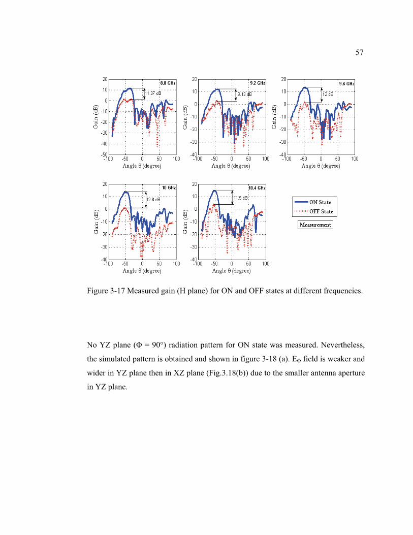
57
Figure 3-17 Measured gain (H plane) for ON and OFF states at different frequencies.
No YZ plane (Φ = 90°) radiation pattern for ON state was measured. Nevertheless,
the simulated pattern is obtained and shown in figure 3-18 (a). EΦ field is weaker and
wider in YZ plane then in XZ plane (Fig.3.18(b)) due to the smaller antenna aperture
in YZ plane.
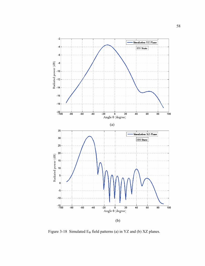
58
(a)
(b)
Figure 3-18 Simulated EΦ field patterns (a) in YZ and (b) XZ planes.
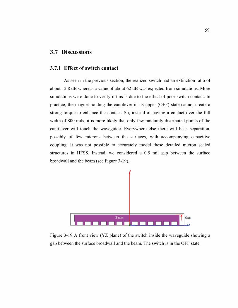
59
3.7 Discussions
3.7.1 Effect of switch contact
As seen in the previous section, the realized switch had an extinction ratio of
about 12.8 dB whereas a value of about 62 dB was expected from simulations. More
simulations were done to verify if this is due to the effect of poor switch contact. In
practice, the magnet holding the cantilever in its upper (OFF) state cannot create a
strong torque to enhance the contact. So, instead of having a contact over the full
width of 800 mils, it is more likely that only few randomly distributed points of the
cantilever will touch the waveguide. Everywhere else there will be a separation,
possibly of few microns between the surfaces, with accompanying capacitive
coupling. It was not possible to accurately model these detailed micron scaled
structures in HFSS. Instead, we considered a 0.5 mil gap between the surface
broadwall and the beam (see Figure 3-19).
Figure 3-19 A front view (YZ plane) of the switch inside the waveguide showing a
gap between the surface broadwall and the beam. The switch is in the OFF state.
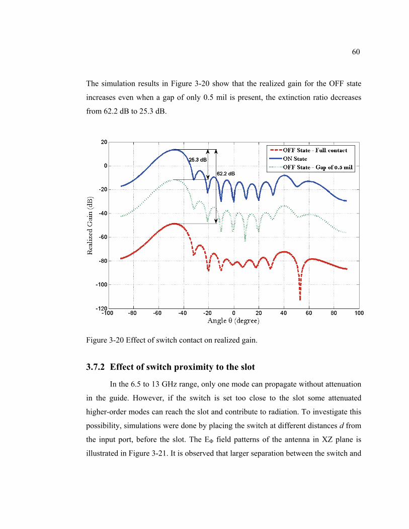
60
The simulation results in Figure 3-20 show that the realized gain for the OFF state
increases even when a gap of only 0.5 mil is present, the extinction ratio decreases
from 62.2 dB to 25.3 dB.
Figure 3-20 Effect of switch contact on realized gain.
3.7.2 Effect of switch proximity to the slot
In the 6.5 to 13 GHz range, only one mode can propagate without attenuation
in the guide. However, if the switch is set too close to the slot some attenuated
higher-order modes can reach the slot and contribute to radiation. To investigate this
possibility, simulations were done by placing the switch at different distances d from
the input port, before the slot. The EΦ field patterns of the antenna in XZ plane is
illustrated in Figure 3-21. It is observed that larger separation between the switch and
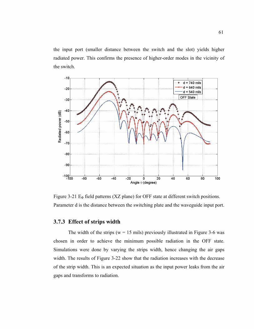
61
the input port (smaller distance between the switch and the slot) yields higher
radiated power. This confirms the presence of higher-order modes in the vicinity of
the switch.
Figure 3-21 EΦ field patterns (XZ plane) for OFF state at different switch positions.
Parameter d is the distance between the switching plate and the waveguide input port.
3.7.3 Effect of strips width
The width of the strips (w = 15 mils) previously illustrated in Figure 3-6 was
chosen in order to achieve the minimum possible radiation in the OFF state.
Simulations were done by varying the strips width, hence changing the air gaps
width. The results of Figure 3-22 show that the radiation increases with the decrease
of the strip width. This is an expected situation as the input power leaks from the air
gaps and transforms to radiation.
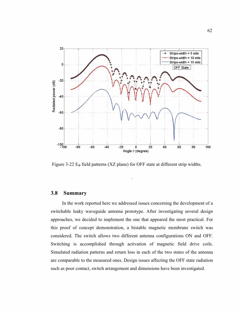
62
Figure 3-22 EΦ field patterns (XZ plane) for OFF state at different strip widths.
.
3.8 Summary
In the work reported here we addressed issues concerning the development of a
switchable leaky waveguide antenna prototype. After investigating several design
approaches, we decided to implement the one that appeared the most practical. For
this proof of concept demonstration, a bistable magnetic membrane switch was
considered. The switch allows two different antenna configurations ON and OFF.
Switching is accomplished through activation of magnetic field drive coils.
Simulated radiation patterns and return loss in each of the two states of the antenna
are comparable to the measured ones. Design issues affecting the OFF state radiation
such as poor contact, switch arrangement and dimensions have been investigated.
63
CHAPTER 4. MEMBRANE-BASED SWITCHED
WAVEGUIDE FILTER 4.1 Introduction
Chapters 2 and 3 have concentrated on a switch membrane and its
incorporation with a leaky waveguide antenna. We have demonstrated its design,
operational principles and implementation. One of the main limitations of the
proposed switch was the difficulty to make a good electrical RF contact between the
moving edge of the cantilever and the waveguide wall. On the other hand, even with
a poor contact, or no contact at all, the presence of a vertical cantilever within the
rectangular waveguide introduces reactive loading. The objective of this chapter is to
investigate the possibility of making use of this switchable reactive element into
waveguide filters. In fact, rectangular waveguide filters are often made of capacitive
irises that are only partially covering the waveguide cross section, i.e. without an
electrical contact from the top to the bottom walls of the guide. The situation is
however somewhat different with our cantilever switch because instead of being
normal to the wall as in irises, our cantilever is making an angle of only 7.66 degrees
with the bottom wall. Consequently, the cantilever in its raised position, which
occupies a length of approximately 1.5 centimeters along the guide, cannot be
represented as a shunt capacitive loading. It is nevertheless a low-loss component
and it may therefore have potential for application in a switched filter. One important
feature of this component is that the electromagnets used to change the state are
located outside the guide. Therefore there are no bias lines inside the propagating
media, as it would be the case with other switching elements such as MEMS,
semiconductor and ferroelectric-based devices used in tuneable filters. This can be a
significant advantage to simplify the design. Furthermore, the cantilever materials are
passive and can therefore exhibit linear operation at higher power levels.
64
In this chapter, we discuss a technique of employing a switch membrane in a
closed waveguide and the potential of this technique in filter design. The switch
geometry is introduced and then used to show a band-stop filter.
4.2 Design and Operation
In order to demonstrate the feasibility of a band stop filter, Figures 4-1(a), (b)
and (c) show the proposed switch incorporated into a closed rectangular waveguide.
We kept the pre-existing waveguide used to demonstrate the antenna prototype in the
previous chapter and added a second transition to the waveguide in order to measure
the transmission. The switch is of type 2, as presented in Figure 2-2. It uses a 1 mil
thickness polyimide (Kapton®) dielectric membrane on one part of the cantilever
while the other part is a single sided copper clad polyimide beam bonded to a
metglas magnetic plate (Fig. 4-1(b)). In the HFSS simulations, the dielectric
membrane is modeled as vacuum (i.e. the membrane is transparent and thin that the
wave can pass through) and the beam along with the metglas are modeled as a PEC.
65
(b)
(c)
Figure 4-1 Membrane switch geometry: (a) screen shot of the HFSS model of the
switch inside the waveguide. (b) Its schematic diagram. The design parameters are
labeled within the drawing. (c) A photograph of the fabricated switch set in the
waveguide.
W = 400 mils
l = 200 mils
L = 400 mils
(a)

66
In the ON state, the switch is in the down position and the wave propagates
through the waveguide. In the OFF state, the movable beam is actuated to move
upward, where its tip makes a dielectric-metal contact with the waveguide broad
wall. This creates reactive loading in the guide that prevents part of the signal from
reaching the output port. It is to be mentioned that in order to avoid the contact
problem encountered in the antenna implementation, the switch in its natural position
(horizontal) is set in a way that the polyimide side of the single sided copper clad
polyimide beam faces the upper broad wall, while its metallic (metglas) side faces
the bottom wall of the waveguide (Fig. 4-1(c)).
In the HFSS simulations, when the switch is in the OFF state, a gap of 1 mil
(polyimide thickness) separates the metallic broad wall and the tip of the movable
beam. Superior gap distances (thicker polyimide) could also be used in order to
facilitate the switch fabrication. However, more energy would be required to actuate
the cantilever.
The switch is magnetically actuated through the magnetization of the Metglas
piece and the switching mechanism introduced in Chapter 3 is used to implement the
displacement of the cantilever and the bi-stability function. The switching currents
used for switching to the OFF and ON states were 30 mA and 110 mA respectively.
4.3 Effect of Switch Length and Position
4.3.1 Effect of varying the length of the movable beam
Simulations were performed for changing the membrane dielectric length l
(Figure 4-1) by keeping the length L of the PEC plate at 400 mils. It was observed
that the variation of the length l enables the adjustment of the filter’s center
frequency. When the length is increased from 100 mils to 250 mils in 50 mils step,
the filter presents the following center frequencies: 10.2 GHz, 10.6 GHz, 10.8 GHz
67
and 11GHz respectively. The return loss and insertion loss characteristics of the filter
when the cantilever in the up (OFF) position are illustrated in Fig. 4-2.
Figure 4-2 Simulated S-parameters for the waveguide, showing the effect of
modifying the length of the dielectric beam. The switch is in the up position.
We adopted the same approach to explore the effect of changing the length L
of the PEC plate and maintaining the dielectric membrane length l at 200 mils. The
simulation results of Figure 4-3 show that as the length decreases, the center
frequency shifts to a higher value.
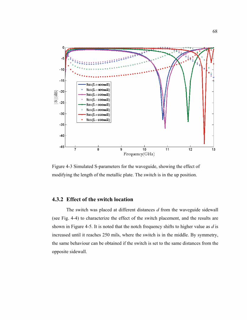
68
Figure 4-3 Simulated S-parameters for the waveguide, showing the effect of
modifying the length of the metallic plate. The switch is in the up position.
4.3.2 Effect of the switch location
The switch was placed at different distances d from the waveguide sidewall
(see Fig. 4-4) to characterize the effect of the switch placement, and the results are
shown in Figure 4-5. It is noted that the notch frequency shifts to higher value as d is
increased until it reaches 250 mils, where the switch is in the middle. By symmetry,
the same behaviour can be obtained if the switch is set to the same distances from the
opposite sidewall.
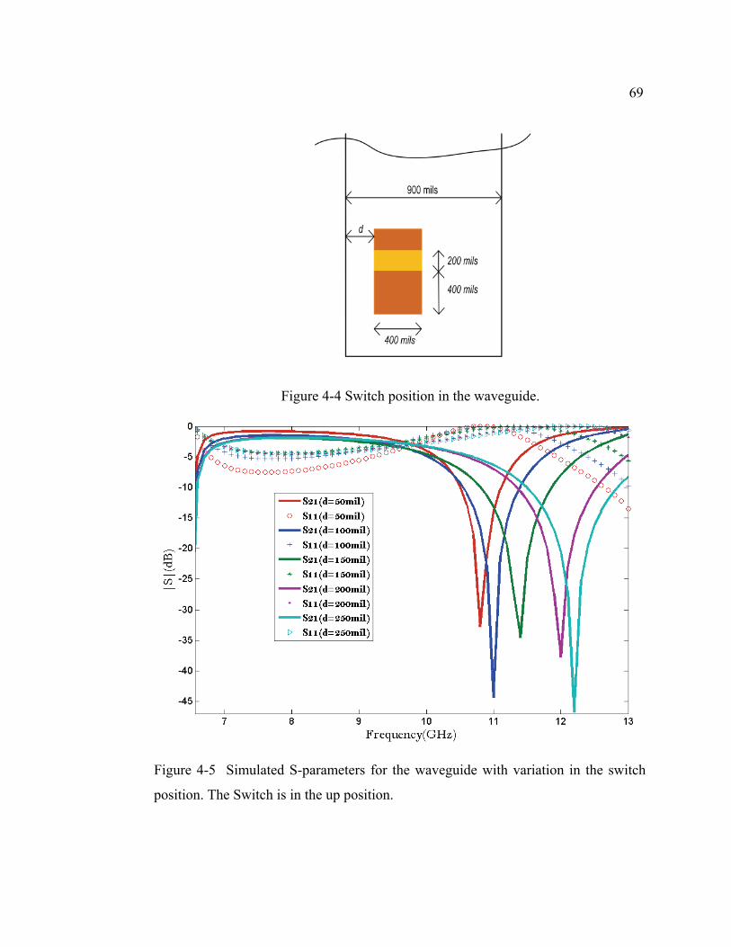
69
Figure 4-4 Switch position in the waveguide.
Figure 4-5 Simulated S-parameters for the waveguide with variation in the switch
position. The Switch is in the up position.
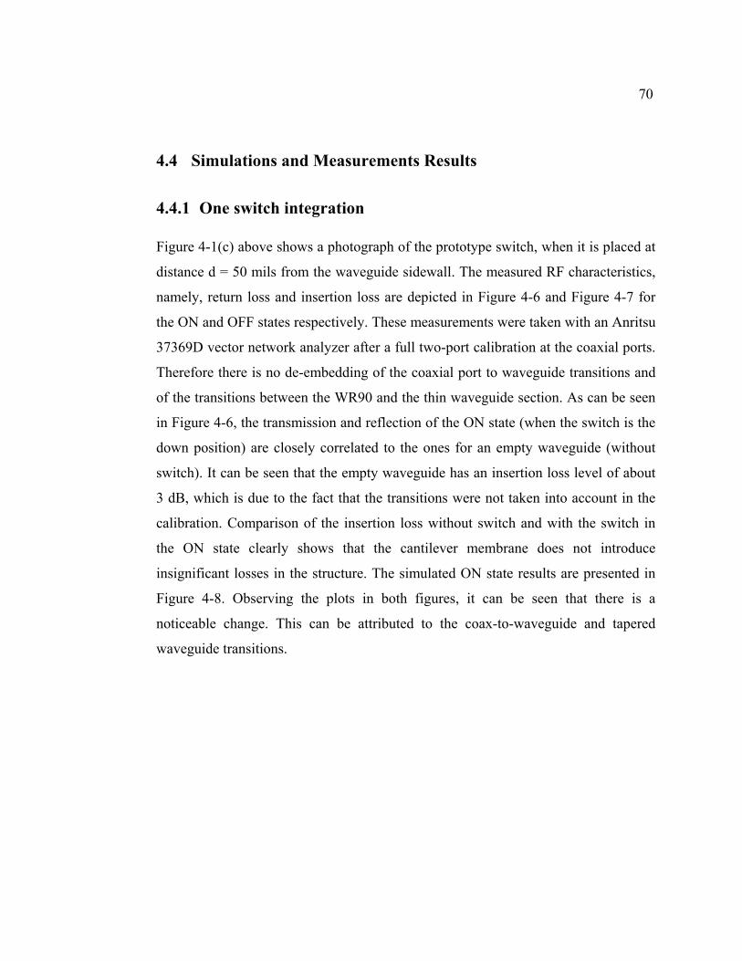
70
4.4 Simulations and Measurements Results
4.4.1 One switch integration
Figure 4-1(c) above shows a photograph of the prototype switch, when it is placed at
distance d = 50 mils from the waveguide sidewall. The measured RF characteristics,
namely, return loss and insertion loss are depicted in Figure 4-6 and Figure 4-7 for
the ON and OFF states respectively. These measurements were taken with an Anritsu
37369D vector network analyzer after a full two-port calibration at the coaxial ports.
Therefore there is no de-embedding of the coaxial port to waveguide transitions and
of the transitions between the WR90 and the thin waveguide section. As can be seen
in Figure 4-6, the transmission and reflection of the ON state (when the switch is the
down position) are closely correlated to the ones for an empty waveguide (without
switch). It can be seen that the empty waveguide has an insertion loss level of about
3 dB, which is due to the fact that the transitions were not taken into account in the
calibration. Comparison of the insertion loss without switch and with the switch in
the ON state clearly shows that the cantilever membrane does not introduce
insignificant losses in the structure. The simulated ON state results are presented in
Figure 4-8. Observing the plots in both figures, it can be seen that there is a
noticeable change. This can be attributed to the coax-to-waveguide and tapered
waveguide transitions.
71
Figure 4-6 Measured S-parameters of the waveguide with switch in the ON state and
without switch.
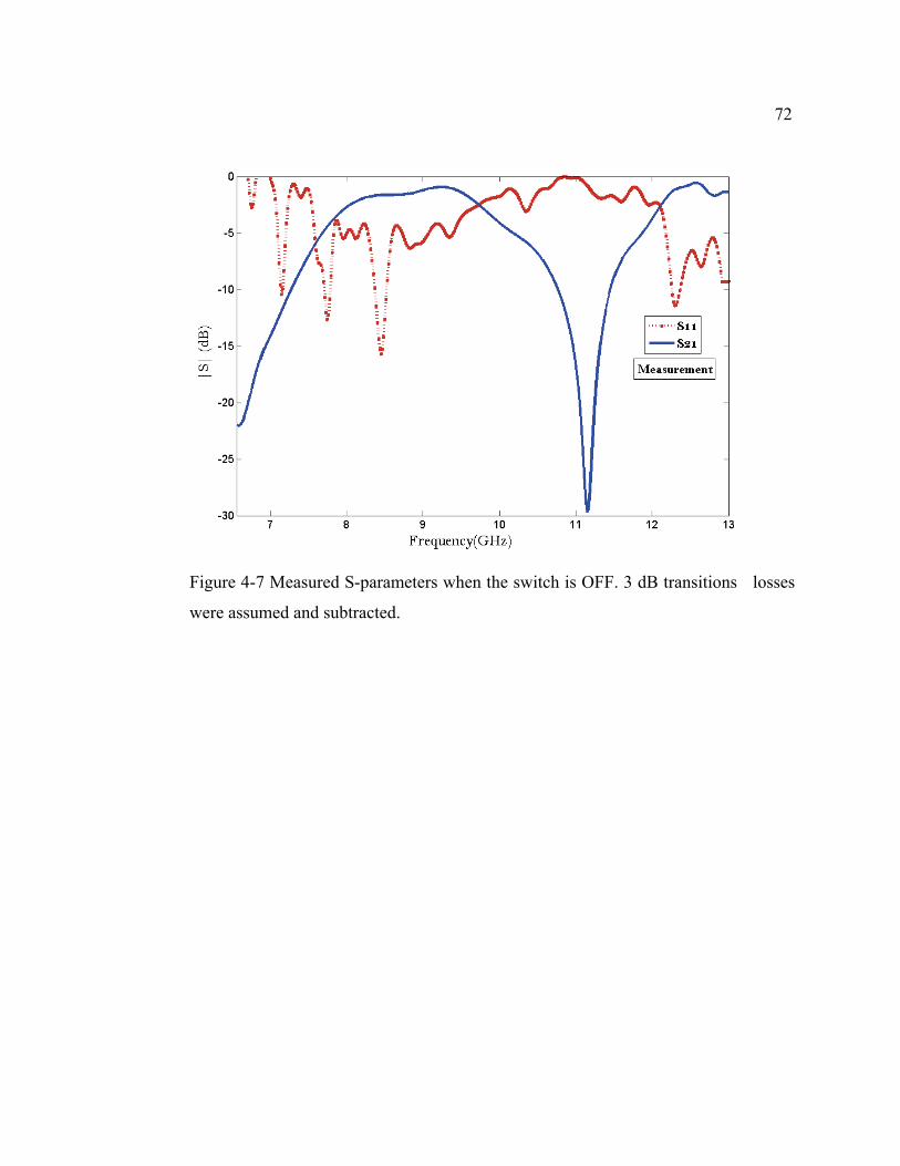
72
Figure 4-7 Measured S-parameters when the switch is OFF. 3 dB transitions losses
were assumed and subtracted.
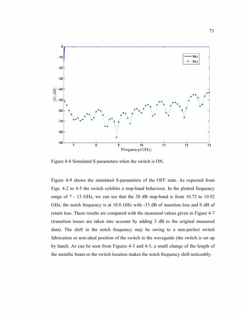
73
Figure 4-8 Simulated S-parameters when the switch is ON.
Figure 4-9 shows the simulated S-parameters of the OFF state. As expected from
Figs. 4-2 to 4-5 the switch exhibits a stop-band behaviour. In the plotted frequency
range of 7 - 13 GHz, we can see that the 20 dB stop-band is from 10.72 to 10.92
GHz, the notch frequency is at 10.8 GHz with -33 dB of insertion loss and 0 dB of
return loss. These results are compared with the measured values given in Figure 4-7
(transition losses are taken into account by adding 3 dB to the original measured
data). The shift in the notch frequency may be owing to a non-perfect switch
fabrication or non-ideal position of the switch in the waveguide (the switch is set up
by hand). As can be seen from Figures 4-3 and 4-5, a small change of the length of
the metallic beam or the switch location makes the notch frequency shift noticeably.
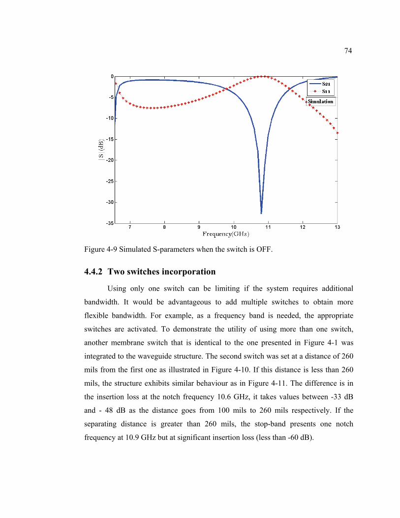
74
Figure 4-9 Simulated S-parameters when the switch is OFF.
4.4.2 Two switches incorporation
Using only one switch can be limiting if the system requires additional
bandwidth. It would be advantageous to add multiple switches to obtain more
flexible bandwidth. For example, as a frequency band is needed, the appropriate
switches are activated. To demonstrate the utility of using more than one switch,
another membrane switch that is identical to the one presented in Figure 4-1 was
integrated to the waveguide structure. The second switch was set at a distance of 260
mils from the first one as illustrated in Figure 4-10. If this distance is less than 260
mils, the structure exhibits similar behaviour as in Figure 4-11. The difference is in
the insertion loss at the notch frequency 10.6 GHz, it takes values between -33 dB
and - 48 dB as the distance goes from 100 mils to 260 mils respectively. If the
separating distance is greater than 260 mils, the stop-band presents one notch
frequency at 10.9 GHz but at significant insertion loss (less than -60 dB).
75
As before, when only one of the switches is activated to be OFF, the
simulated transmission exhibits a 20 dB stop-band bandwidth of 0.2 GHz. However,
when the two switches are activated, this 20 dB bandwidth is extended to 0.9 GHz.
Frequency responses of the modeled S11 and S21 magnitudes are shown in Figure 4-
11. Those results are compared to measurements shown in Figure 4-12. From this
Figure, it can be noticed that the 20 dB stop-band bandwidth is of 0.2 GHz when
only one switch is operated to be OFF, and 0.9 GHz when both switches are OFF
(the 3 dB transition losses are taken into consideration). Therefore, the simulated 20
dB stop-band bandwidth follows closely the measured ones. A comparison of
measurements and simulations of the proposed switches shows that except for the 20
dB stop-bandwidth, the measured results show inferior pass-band and stop-band
performance compared to the modeled ones. The S21 notch has changed to 11.1 GHz
from of 10.8 GHz. The reason for this discrepancy could be attributed to the
aforementioned aspects such as switch fabrication uncertainties, non ideal switch
placement and the use of the tapered transitions.
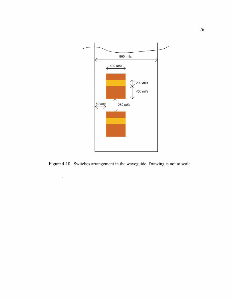
76
Figure 4-10 Switches arrangement in the waveguide. Drawing is not to scale.
.
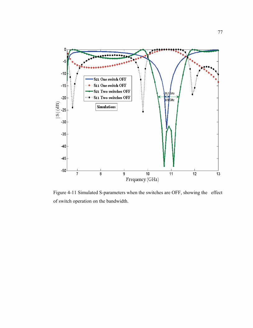
77
Figure 4-11 Simulated S-parameters when the switches are OFF, showing the effect
of switch operation on the bandwidth.
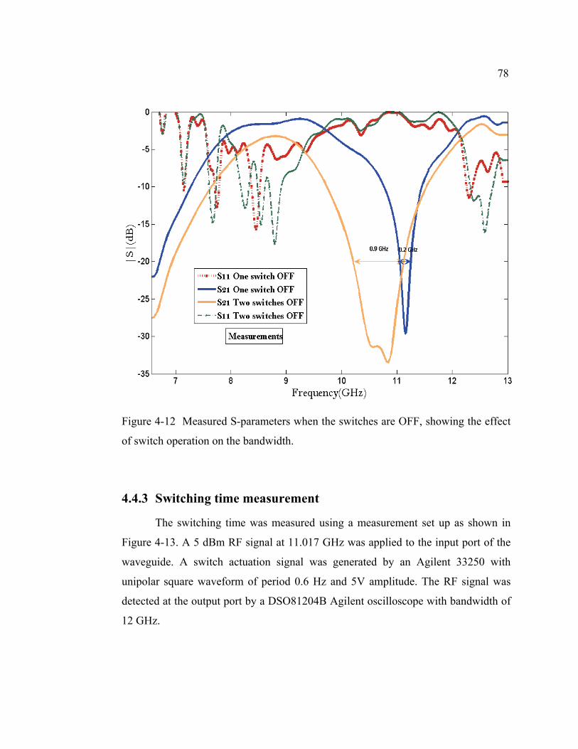
78
Figure 4-12 Measured S-parameters when the switches are OFF, showing the effect
of switch operation on the bandwidth.
4.4.3 Switching time measurement
The switching time was measured using a measurement set up as shown in
Figure 4-13. A 5 dBm RF signal at 11.017 GHz was applied to the input port of the
waveguide. A switch actuation signal was generated by an Agilent 33250 with
unipolar square waveform of period 0.6 Hz and 5V amplitude. The RF signal was
detected at the output port by a DSO81204B Agilent oscilloscope with bandwidth of
12 GHz.

79
Figure 4-13 Switching time measurement setup.
Figure 4-14 shows the detected RF signal and Figures 4-15(a) and (b)
illustrate the measured switching times toff and ton respectively. The toff is 80 ms for
the transition from the ON to the OFF state and ton is 3ms for the transition from the
OFF to the ON state. This difference is due to the mechanical oscillations (bouncing)
that occur before the switch settles into the upper position (OFF state).
This test was running for 1 hour duration with no RF performance degradation, nor
switch deformation. Therefore, the fabricated switch showed good mechanical
performance.
5 dBm at 11.017 GHz
Coil
0 – 5V, 0.6 Hz Agilent
33250
RF source Switch integrated into
the waveguide Oscilloscope
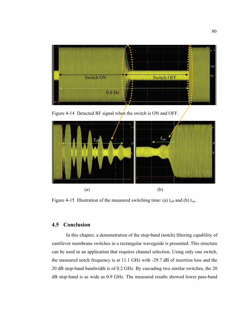
80
Figure 4-14 Detected RF signal when the switch is ON and OFF.
(a) (b)
Figure 4-15 Illustration of the measured switching time: (a) toff and (b) ton.
4.5 Conclusion
In this chapter, a demonstration of the stop-band (notch) filtering capability of
cantilever membrane switches in a rectangular waveguide is presented. This structure
can be used in an application that requires channel selection. Using only one switch,
the measured notch frequency is at 11.1 GHz with -29.7 dB of insertion loss and the
20 dB stop-band bandwidth is of 0.2 GHz. By cascading two similar switches, the 20
dB stop-band is as wide as 0.9 GHz. The measured results showed lower pass-band
Switch ON Switch OFF
toff ton
0.6 Hz

81
and stop-band performance when compared to the simulated ones, owing to the
switch fabrication uncertainties. The measured switching times are 3 ms for the
transition from the OFF to the ON state and 80 ms for the transition from the ON to
the OFF state.
82
CHAPTER 5. CONCLUSIONS
5.1 Thesis Contributions
This project has focused on developing a latching magnetic RF waveguide
switch built on a flexible membrane. Two distinct switch geometries have been
investigated by simulations and experiments: one in a leaky waveguide antenna and
the other in a closed waveguide filtering structure. Both geometries offered an out-of
plane displacement of 2 mm of the flexible membrane at driving currents of 40 mA
(max.) for switching from ON to the OFF state and 140 mA (max.) for switching
from the OFF to the ON state. The latched state was maintained with a permanent
magnet generating a flux density of 2.55 mT in the vicinity of the magnetically
actuated membrane.
A switched antenna was designed, fabricated and tested. Simulations and
measurements showed similar gains (~13 dB) and comparable radiation patterns
when the switch is in the ON state. However, the experimental characterization
highlighted the difficulty of achieving the OFF state antenna characteristics predicted
by simulations. This was due to a non-perfect electrical contact between the tip of the
cantilever and waveguide broad-wall. Overall, the concept of a switched antenna
using this type of switch was proven but more work is needed to overcome this
contact problem.
The demonstrated membrane switch could be a potential candidate for reconfigurable
antennas. As this switch does not have any electronic components, the interference
coming from its environment will not be a concern. One of the most interesting
characteristics of the proposed switch is its negligible loss. This allows its integration
into antenna feeding networks.
83
The second part of this research dealt with the demonstration of a stop-band
filter, implemented using a variable reactance membrane switch in a closed
rectangular waveguide. Fortunately, with this switch configuration, we were able to
surmount the aforementioned metal-metal contact problem, as the moving cantilever
makes a dielectric-metal contact with the waveguide broad-wall. The measured
results verify the concept demonstrating an insertion loss of -29.7 dB at a notch
frequency of 11.1 GHz and a 20 dB stop-band bandwidth of 0.2 GHz. By using two
cascaded switches, this bandwidth was extended to 0.9 GHz. Measured switching
time were 3 ms from the OFF to the ON state and 80 ms from the ON to the OFF
state.
5.2 Future Work
Even though the proposed switches demonstrated promising results, a few
issues still need to be further addressed.
Antenna switch
The reconfigurable antenna did not work as expected. This is due to a non
perfect contact between the tip of the cantilever and the waveguide broad-wall in the
OFF state. Future efforts can be directed towards developing a technique to enhance
this electrical contact.
Variable reactance switch
For improving the switching time from ON to OFF, suppression of bounce
duration is required. An approach to minimize this duration may be the use of a very
high permeability magnetic material. This will provide low actuation voltage and fast
settling time. It has been demonstrated in section 4.3 that different sized membranes
give varied notch frequencies. By cascading set of dissimilar (in dimensions)
membrane switches, a tunable band stop filter can be implemented. This would be a
completion of what has been done in this work regarding variable reactance
84
membrane switch. Another possible research direction could be to derive an
equivalent electric circuit model of the flexible beam in the upright position. With
such a model, it would be possible to use filter synthesis software tools to assist in
the design of the proposed reconfigurable filters. Without such models, design would
only be possible with time consuming electromagnetic simulations.
As indicated in Chapter 1, the majority of the devices currently used in
reconfigurable RF components (MEMS, PIN diodes, varactors, FETs) have severe
power limitations. The switching elements presented here are operating in a
rectangular waveguide which is well known for its high power handling capability.
In addition, all the parts of the switch exposed to the RF field are passive. We can
therefore anticipate that it will exhibit linear operation at high power levels before
deleterious effects such as passive intermodulation or electrical breakdown occur.
Unfortunately, it was not possible to verify this conjecture because high-power X-
band generators are not available in our laboratory. Should such generators become
available to the research team, future work should then include tests to verify the real
power handling of the flexible switch devices we have proposed.
85
REFERENCES
[1] D. Lichodziejewski, R. Cravey, G. Hopkins, "Inflatably Deployed Membrane
Waveguide Array Antenna for Space” AIAA 2003-1649, 4th Gossamer Spacecraft Forum,
April 7-10, 2003, Norfolk, VA.
[2] M. Leipold, H. Runge, and C. Sickinger, "Large SAR Membrane Antennas with
Lightweight Deployable Booms," 28th ESA Antenna Workshop on Space Antenna Systems
and Technologies, ESA/ESTEC, May 31 –June 03, 2005.
[3] D. Fralick, R.L. Cravey, G. Hopkins, D. Lichodziejewski, M. C. Bailey, “Performance
Evaluation of a Membrane Waveguide Array Antenna”, IEEE-2003-1148 IEEE Aerospace
Conference, March 8 2003, WY
[4] M.C. Bailey and T. G. Campbell, "Inflatable Membrane Waveguide Antenna Array for
Space applications" IUTAM-IASS Symposium on Deployable Structures, Cambridge, UK,
September 6-9, 1998.
[5] A.Di. Maria, M. Limbach, R. Horn, A. Reigber, "Reflectarray membrane study for
deployable SAR antenna," Antennas and Propagation, 2009. EuCAP 2009. 3rd European
Conference on, vol., no., pp.3720-3723, 23-27 March 2009
[6] B.M. Kendall, M.C. Bailey, L.C. Schroeder, "Inflatable antenna microwave radiometer
for soil moisture measurement," Combined Optical-Microwave Earth and Atmosphere
Sensing, 1995. Conference Proceedings., Second Topical Symposium on , vol., no., pp.217-
219, 3-6 Apr 1995
86
[7] M. Leipold, M. Eiden, CE. Garner, L.Herbeck, "Solar Sail Technology Development
and Demonstration", 4th IAA International Conference on Low-Planetary Missions, May
2-5, 2000, Johns Hopkins University, Maryland, USA, IAA 2000, Paper 0707
[8] G.M. Rebeiz, RF MEMS: Theory, Design and Technology; Wiley: Hoboken, NJ, USA,
2003.
[9] J.B. Rizk, E. Chaiban, G.M. Rebeiz "Steady state thermal analysis and high-power
reliability considerations of RF MEMS capacitive switches," Microwave Symposium
Digest, 2002 IEEE MTT-S International , vol.1, no., pp.239-242, 2002
[10] W.Thiel, K. Tornquist, R. Reano, L.P.B "Katehi A Study of Thermal Effects in RF-
MEMSwitches Using a Time Domain Approach", In Proceedings of the IEEE MTT-S
International Microwave Symposium, Seattle, WA, USA, 2002; pp. 235-238.
[11] C.T.-C. Nguyen, L.P.B. Katehi, G.M. Rebeiz, "Micromachined devices for wireless
communications," Proceedings of the IEEE , vol.86, no.8, pp.1756-1768, Aug 1998
[12] P.M. Zavracky, N.E. McGruer, R.H. Morrison, and D. Potter, "Microswitches and
Microrelays with a View Toward Microwave Applications, " International Journal of RF
and Microwave Computer Aided Design, vol. 9, no. 4, pp. 338– 347, July 1999.
[13] S. Duffy, C. Bozler, S. Rabe, J. Knecht, L. Travis, P. Wyatt, C. Keast, M. Gouker,
"MEMS microswitches for reconfigurable microwave circuitry," Microwave and Wireless
Components Letters, IEEE , vol.11, no.3, pp.106-108, Mar 2001
87
[14] C.L. Goldsmith, Z. Yao, S. Eshelman, and D. Denniston, "Performance of Lowloss RF
MEMS Capacitive Switches, " IEEE Microwave and Guided Wave Letters, vol. 8, no. 8,
pp. 269–271, August 1998.
[15] S.J. Gross, Q.Q. Zhang, S. Trolier-McKinstry, S. Tadigadapa, T.N. Jackson, "RF
MEMS piezoelectric switch," Device Research Conference, 2003 , vol., no., pp. 99- 100,
23-25 June 2003
[16] G.M. Rebeiz, RF MEMS: Theory, Design and Technology, John Wiley & Sons, Inc.,
Hoboken, NJ, USA, 2003
[17] R.R. Mansour, "RF MEMS for space applications," MEMS, NANO and Smart
Systems, 2005. Proceedings. 2005 International Conference on, vol., no., pp. 191- 192, 24-
27 July 2005
[18] Z. Jun, L. Chang, J. Schutt-Aine, C. Jinghong, K. Sung-Mo, "Development of a wide
tuning range MEMS tunable capacitor for wireless communication systems," Electron
Devices Meeting, 2000. IEDM Technical Digest. International, vol., no., pp.403-406, 2000
[19] R. Zhang, R.R Mansour, "Novel digital and analogue tunable lowpass filters,"
Microwaves, Antennas & Propagation, IET , vol.1, no.3, pp.549-555, June 2007
[20] A. Ocera, P. Farinelli, P. Mezzanotte, R. Sorrentino, B. Margesin, F. Giacomozzi, "A
Novel MEMS-Tunable Hairpin Line Filter on Silicon Substrate," Microwave Conference,
2006. 36th European, vol., no., pp.803-806, 10-15 Sept. 2006
88
[21] C.Y. Ong; M. Okoniewski, "Low loss switchable coupled resonator bandpass filter,"
Microwave Symposium Digest, 2008 IEEE MTT-S International , vol., no., pp.137-140, 15-
20 June 2008
[22] J. Nath, D. Ghosh, J.-P. Maria, A.I. Kingon, W. Fathelbab, P.D. Franzon, M.B. Steer,
"An electronically tunable microstrip bandpass filter using thin-film Barium-Strontium-
Titanate (BST) varactors," Microwave Theory and Techniques, IEEE Transactions on ,
vol.53, no.9, pp. 2707- 2712, Sept. 2005
[23] A. Tombak, J.-P. Maria, F.T. Ayguavives, Jin. Zhang Jin, G.T. Stauf, A.I. Kingon, A.
Mortazawi, "Voltage-controlled RF filters employing thin-film barium-strontium-titanate
tunable capacitors," Microwave Theory and Techniques, IEEE Transactions on , vol.51,
no.2, pp. 462- 467, Feb. 2003
[24] Y.Lu " RF MEMS Devices and their applications in reconfigurable RF/Microwave
circuits", Ph.D. dissertation, University of Michigan, 2005.
[25] R. Jakoby, P. Scheele, S. Muller, C. Weil, "Nonlinear dielectrics for tunable
microwave components," Microwaves, Radar and Wireless Communications, 2004.
MIKON-2004. 15th International Conference on, vol.2, no., pp. 369- 378 Vol.2, 17-19 May
2004
[26] G.M. Rebeiz, J.B. Muldavin, "RF MEMS switches and switch circuits," Microwave
Magazine, IEEE, vol.2, no.4, pp.59-71, Dec 2001
[27] M. Ruan, J. Shen, and C.Wheeler, "Latching Micro Electromagnetic Relays,” Solid-
State Sensor and Actuator Workshop (Hilton Head 2000), Hilton Head Island, SC (June 4-
8, 2000), pp.146-149
89
[28] R. Holzer, I. Shimoyama, H. Miura, "Hybrid electrostatic/magnetic microactuators,"
Robotics and Automation, 1995. Proceedings, 1995 IEEE International Conference on ,
vol.3, no., pp.2941-2946 vol.3, 21-27 May 1995
[29] C. Il-Joo, S. Taeksang, B. Sang-Hyun, Y. Euisik, "A low-voltage and low-power RF
MEMS series and shunt switches actuated by combination of electromagnetic and
electrostatic forces," Microwave Theory and Techniques, IEEE Transactions on , vol.53,
no.7, pp. 2450- 2457, July 2005
[30] J.G. Smits, S.I. Dalke, "The constituent equations of piezoelectric bimorphs,"
Ultrasonics Symposium, 1989. Proceedings., IEEE 1989, vol., no., pp.781-784 vol.2, 3-6
Oct 1989
[31] M.S. Weinberg, "Working equations for piezoelectric actuators and sensors,"
Microelectromechanical Systems, Journal of , vol.8, no.4, pp.529-533, Dec 1999
[32] D.L. DeVoe, A.P. Pisano, "Modeling and optimal design of piezoelectric cantilever
microactuators," Microelectromechanical Systems, Journal of , vol.6, no.3, pp.266-270,
Sep 1997
[33] S.J. Gross, S. Tadigadapa, T.N. Jackson, S. Trolier-McKinstry, Q.Q. Zhang, "Lead-
zirconate-titanate-based piezoelectric micromachined switch," Applied Physics Letters ,
vol.83, no.1, pp.174-176, Jul 2003
[34] F.C.M van de Pol, H.T.G van Lintel, M. Elvenspoek, J.H.J. Fluitman,
“Thermopneumatic micropump based on micro-engineering techniques,” Sensors and
Actuators A, 21, pp.198, 1990.

90
[35] http://webdocs.cs.ualberta.ca/~database/MEMS/sma_mems/sma.html [Consulted on
August 9, 2010]
[36] N. Camara, K. Zekentes, L.P. Romanov, A.V. Kirillov, M.S. Boltovets, K.V.
Vassilevski, G. Haddad, "Microwave p-i-n diodes and switches based on 4H-SiC," Electron
Device Letters, IEEE , vol.27, no.2, pp. 108- 110, Feb. 2006
[37] E.W. Jacobs, D.W. Fogliatti, H. Nguyen, D.J. Albares, C.K. Sun, C.T. Chang, "Photo-
injection PIN diode switch for high power RF switching," Solid-State and Integrated-
Circuit Technology, 2001. Proceedings. 6th International Conference on, vol.2, no., pp.
1274- 1279 vol.2, 22-25 Oct. 2001
[38] K. Miyatsuji, S. Nagata, N. Yoshikawa, K. Miyanaga, Y. Ohishi, D. Ueda, "A GaAs
high-power RF single-pole double-throw switch IC for digital mobile communication
system," Solid-State Circuits Conference, 1994. Digest of Technical Papers. 41st ISSCC.,
1994 IEEE International , vol., no., pp.34-35, 16-18 Feb 1994
[39] Eng Kai Eng, T. Stern, "The Order-and-Type Prediction Problem Arising from Passive
Intermodulation Interference in Communications Satellites," Communications, IEEE
Transactions on , vol.29, no.5, pp. 549- 555, May 1981
[40] Kai Y. Eng, On-Ching Yue, "High-Order Intermodulation Effects in Digital Satellite
Channels," Aerospace and Electronic Systems, IEEE Transactions on , vol.AES-17, no.3,
pp.438-445, May 1981
[41] http://www2.dupont.com/Pyralux/en_US/products/laminate/index.html [Consulted on
October 15, 2009]

91
[42] http://metglas.com/products/page5_1_2.htm [Consulted on November 5, 2009]
[43] R. Frisch-Fay, Flexible Bars, London, U.K: Butterworth, 1962.
[44] Crandall, S. H, Dahl, N. C. & Lardner, T. J. (1978) An Introduction to the Mechanics
of Solids (McGraw–Hill, New York).
[45] http://en.wikipedia.org/wiki/Young's_modulus [Consulted on November 5, 2009]
[46] J.H. Schaffner, R.Y. Loo, D.F. Sievenpiper, F.A. Dolezal, G.L. Tangonan, J.S.
Colburn, J.J. Lynch, J.J. Lee, S.W. Livingston, R.J. Broas, M. Wu, "Reconfigurable
aperture antennas using RF MEMS switches for multi-octave tunability and beam steering,"
Antennas and Propagation Society International Symposium, 2000. IEEE, vol.1, no.,
pp.321-324 vol.1, 2000
[47] K.C. Gupta, Li. Jun, R. Ramadoss, W. Chunjun, "Design of frequency-reconfigurable
rectangular slot ring antennas," Antennas and Propagation Society International
Symposium, 2000. IEEE , vol.1, no., pp.326 vol.1, 2000
[48] D. Sievenpiper, J. Schaffner, B. Loo, G. Tangonan, R. Harold, J. Pikulski, R. Garcia,
"Electronic beam steering using a varactor-tuned impedance surface ," Antennas and
Propagation Society International Symposium, 2001. IEEE , vol.1, no., pp.174-177 vol.1,
2001