Embed Size (px)
Citation preview
1SPRAC85–May 2017Submit Documentation Feedback
Copyright © 2017, Texas Instruments Incorporated
Bidirectional DC-AC Solution For Solar Application System, Based on theTMS320F28035 MCU
Application ReportSPRAC85–May 2017
Bidirectional DC-AC Solution For Solar ApplicationSystem, Based on the TMS320F28035 MCU
TerryDeng
ABSTRACTThis application note presents a detailed solution for implementing a 3-phase solar inverter applicationsystem based on the TMS320F28035 microcontrollers (MCUs). The solution design includes bidirectional3-phase DC-AC algorithms, and the maximum power point tracking (MPPT) DC-DC algorithm for solarpanel control.
The solar inverter has gained more and more attention in recent years. The solar inverter gets the solarenergy input, then it feeds the solar energy to the grid. Grid-tie technology and protection are keyconsiderations when designing a solar inverter system. This solution implements an isolated DC-DC stagewith the MPPT algorithm, to make use of the full capacity of the solar panel. The solar inverter maintainsits input voltage at the reference set point generated by the MPPT algorithm, and delivers power to adownstream DC-AC inverter when connected across its output. The bidirecion DC-AC inverter transferspower from the DC stage to the connected AC grid while the DC loading requirement is small. Or, theinverter transfers the power from the connected AC grid to the DC stage if the DC energy is insufficient forthe DC loading requirement.
In this document, basic knowledge of the inverter is presented first. The hardware introduction, firmwaredesign, and closed-loop controllers design is also described. Lastly, the test results and the waveform areshown.
www.ti.com
2 SPRAC85–May 2017Submit Documentation Feedback
Copyright © 2017, Texas Instruments Incorporated
Bidirectional DC-AC Solution For Solar Application System, Based on theTMS320F28035 MCU
Contents1 Introduction ................................................................................................................... 32 System Specification ........................................................................................................ 33 MCU Use Overview ......................................................................................................... 44 Hardware Design ............................................................................................................ 55 Firmware Design ........................................................................................................... 126 Final Product Performance................................................................................................ 207 Related Documentation.................................................................................................... 22
List of Figures
1 System Overview Block..................................................................................................... 32 DC-AC Circuit Structure .................................................................................................... 53 Circuit Analysis for Arm On................................................................................................. 64 Circuit Analysis for Arm Off................................................................................................. 65 3-Phase Bridge Driver Circuit .............................................................................................. 76 Boost Driver Circuit .......................................................................................................... 87 Voltage Signal Sample Circuit ............................................................................................. 98 Current Signal Sample Circuit ............................................................................................ 109 AC Waveform Frequency Detection Circuit............................................................................. 1110 DC-AC Equivalent.......................................................................................................... 1211 Current and Voltage Phase Relationship ............................................................................... 1212 Software Main Process Flow ............................................................................................. 1313 Current Closed Loop Flow ................................................................................................ 1414 Lap Conversion Diagram.................................................................................................. 1515 Closed-Loop Diagram ..................................................................................................... 1516 Simplified Control Loop.................................................................................................... 1517 Current Loop Controller Analysis......................................................................................... 1618 V-I Curves for Solar Cell .................................................................................................. 1619 DC-DC Control Loop Diagram............................................................................................ 1720 MPPT Algorithm Flow ..................................................................................................... 1821 Current and Voltage Waveform in PFC Mode.......................................................................... 2022 Current and Voltage Waveform in Translation Mode.................................................................. 2123 Current and Voltage Waveform in Inverter Mode ...................................................................... 21
List of Tables
1 System Specification ........................................................................................................ 32 MCU Pin Assignment........................................................................................................ 4
TrademarksPiccolo is a trademark of Texas Instruments.All other trademarks are the property of their respective owners.
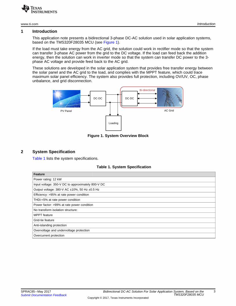
PV Panel
DC-DC DC-DC
Loading
AC Grid
Bi-directional
www.ti.com Introduction
3SPRAC85–May 2017Submit Documentation Feedback
Copyright © 2017, Texas Instruments Incorporated
Bidirectional DC-AC Solution For Solar Application System, Based on theTMS320F28035 MCU
1 IntroductionThis application note presents a bidirectional 3-phase DC-AC solution used in solar application systems,based on the TMS320F28035 MCU (see Figure 1).
If the load must take energy from the AC grid, the solution could work in rectifier mode so that the systemcan transfer 3-phase AC power from the grid to the DC voltage. If the load can feed back the additionenergy, then the solution can work in inverter mode so that the system can transfer DC power to the 3-phase AC voltage and provide feed back to the AC grid.
These solutions are developed in the solar application system that provides free transfer energy betweenthe solar panel and the AC grid to the load, and complies with the MPPT feature, which could tracemaximum solar panel efficiency. The system also provides full protection, including OV/UV, OC, phaseunbalance, and grid disconnection.
Figure 1. System Overview Block
2 System SpecificationTable 1 lists the system specifications.
Table 1. System Specification
FeaturePower rating: 12 kWInput voltage: 350-V DC to approximately 800-V DCOutput voltage: 380-V AC ±10%, 50 Hz ±0.5 HzEfficiency: >95% at rate power conditionTHDi:<5% at rate power conditionPower factor: >99% at rate power conditionNo transform isolation structure:MPPT featureGrid-tie featureAnti-islanding protectionOvervoltage and undervoltage protectionOvercurrent protection

MCU Use Overview www.ti.com
4 SPRAC85–May 2017Submit Documentation Feedback
Copyright © 2017, Texas Instruments Incorporated
Bidirectional DC-AC Solution For Solar Application System, Based on theTMS320F28035 MCU
3 MCU Use OverviewThe F2803x Piccolo™ family of microcontrollers from TI provides the power of the C28x core and controllaw accelerator (CLA), coupled with highly integrated control peripherals in low pin-count devices. Thisfamily is code-compatible with previous C28x-based code, and provides a high level of analog integration.
An internal voltage regulator allows for single rail operation. Enhancements have been made to theHRPWM module to allow for dual-edge control (frequency modulation). Analog comparators with internal10-bit references have been added and can be routed directly to control the PWM outputs. The ADCconverts from 0- to 3.3-V fixed full-scale range and supports ratio-metric VREFHI and VREFLOreferences. The ADC interface has been optimized for low overhead and latency.• High-efficiency 32-bit CPU, 60-MHz device, CLA• Single 3.3-V supply, no power-sequencing requirement• Two internal zero-pin oscillators, missing clock detection circuitry• On-chip flash, SARAM, OTP memory, 128-bit security key/lock• Serial port peripherals input (1x SCI, 2x SPI, 1x I2C, 1x LIN, 1x eCAN)• Enhanced pulse width modulator (ePWM), high-resolution PWM (HRPWM)• Enhanced capture (eCAP) module, high-resolution input capture (HRCAP) module• Enhanced quadrature encoder pulse (eQEP) supports all peripheral interrupts• Analog-to-digital converter (ADC)• On-chip temperature sensor module, comparator• 56-, 64-, and 80-pin packages
Table 2 lists the pin assignment for the bidirectional DC-AC inverter system.
Table 2. MCU Pin Assignment
Pin No. Peripherals Pin No. Signal Name Function18
ADC
ADCINA0 I_R R-phase current17 ADCINA1 I_S S-phase current16 ADCINA2 I_T T-phase current
15 ADCINA3 V_RS Voltage between R-Sphase
14 ADCINA4 V_ST Voltage between S-Tphase
13 ADCINA5 V_TR Voltage between T-Rphase
12 ADCINA6 V_DC DC BUS voltage11 ADCINA7 I_DC DC BUS current24 ADCINB1 TEMP_EVM IPM temperature25 ADCINB2 TEMP_CASE Sink temperature26 ADCINB3 V_PV1 Voltage of first PV panel27 ADCINB4 I_PV1 Current of first PV panel
28 ADCINB5 I_PV2 Current of second PVpanel
29 ADCINB6 V_PV2 Voltage of second PVpanel
55 Capture ECAP1 V_RS_ZERO RS-phase voltage zerocrossing
47 Ext_Int TZ1 FO Error external trigger

www.ti.com Hardware Design
5SPRAC85–May 2017Submit Documentation Feedback
Copyright © 2017, Texas Instruments Incorporated
Bidirectional DC-AC Solution For Solar Application System, Based on theTMS320F28035 MCU
Table 2. MCU Pin Assignment (continued)Pin No. Peripherals Pin No. Signal Name Function69
EPWM
PWM1A RH R-phase up IGBT driver68 PWM1B RL R-phase low IGBT driver67 PWM2A SH S-phase up IGBT driver66 PWM2B SL S-phase low IGBT driver63 PWM3A TH T-phase up IGBT driver62 PWM3B TL T-phase low IGBT driver
50 PWM4A IGBT_1 First PV panel DC-DCIGBT driver
43 PWM5A IGBT_2 Second PV panel DC-DC IGBT driver
41
GPIO
GPIO18 RLY_T T-phase relay driver42 GPIO17 RLY_S S-phase relay driver44 GPIO25 RLY_R R-phase relay driver
45 GPIO44 RLY_1 First PV panel relaydriver
46 GPIO16 RLY_2 Second PV panel relaydriver
48 GPIO41 LED_1 Run status display49 GPIO7 LED_2 Fault error display34
SCISCITXDA TXD UART transfer
40 SCIRXDA RXD UART receiver
4 Hardware Design
4.1 Basic System Topology IntroduceFigure 2 shows the basic system topology implementing a 3-phase DC-AC converter.
Figure 2. DC-AC Circuit Structure

Hardware Design www.ti.com
6 SPRAC85–May 2017Submit Documentation Feedback
Copyright © 2017, Texas Instruments Incorporated
Bidirectional DC-AC Solution For Solar Application System, Based on theTMS320F28035 MCU
Figure 3 shows an example description of the topology working principle. When Q2 is on, the L1 inductorcurrent raises, the current flows from R phase, and then goes through the Q4 or Q6 body diode, and atlast gets into S or T phase. Then the energy is stored in the L1 inductor.
Figure 3. Circuit Analysis for Arm On
When Q2 is off, the L1 inductor current falls, the current flow goes through the capacitor, and then gets toS or T phase (see Figure 4). The energy stored in the L1 inductor is released.
Figure 4. Circuit Analysis for Arm Off

www.ti.com Hardware Design
7SPRAC85–May 2017Submit Documentation Feedback
Copyright © 2017, Texas Instruments Incorporated
Bidirectional DC-AC Solution For Solar Application System, Based on theTMS320F28035 MCU
4.2 MCU Key Peripheral Module
4.2.1 3-Phase Bridge Power Switcher CircuitOne ePWM module can output two PWM signals with dead-time complementation: EPWMxA andEPWMxB. Three ePWM modules are used to generate six PWM signals as UP and UN; VP and VN; andWP and WN, to drive the 3-phase power module (PM50CLA120), as shown in Figure 5, and switch thePN DC 700 V to the U/V/W AC 380 V port directly. The three ePWM modules are chained togetherthrough a clock synchronization scheme that allows six PWM signals and the frequency must be aligned.
Figure 5. 3-Phase Bridge Driver Circuit
sprac85_
Hardware Design www.ti.com
8 SPRAC85–May 2017Submit Documentation Feedback
Copyright © 2017, Texas Instruments Incorporated
Bidirectional DC-AC Solution For Solar Application System, Based on theTMS320F28035 MCU
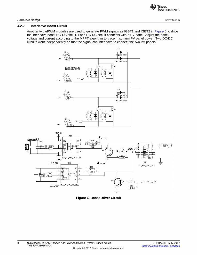
4.2.2 Interleave Boost CircuitAnother two ePWM modules are used to generate PWM signals as IGBT1 and IGBT2 in Figure 6 to drivethe interleave boost DC-DC circuit. Each DC-DC circuit connects with a PV panel. Adjust the panelvoltage and current according to the MPPT algorithm to trace maximum PV panel power. Two DC-DCcircuits work independently so that the signal can interleave to connect the two PV panels.
Figure 6. Boost Driver Circuit

www.ti.com Hardware Design
9SPRAC85–May 2017Submit Documentation Feedback
Copyright © 2017, Texas Instruments Incorporated
Bidirectional DC-AC Solution For Solar Application System, Based on theTMS320F28035 MCU
4.2.3 Voltage Signal Sample CircuitThree voltage phases (R, S, and T) and two solar panel voltages are sampled by both the internal 12-bitADC of the F28035 device. A series resistor divider with different schemes is designed to adjust thesample signal range and filter the noise. Then, it transfers the two single signals through the externalOPAMP and input to the MCU ADC (see Figure 7).
Figure 7. Voltage Signal Sample Circuit

Hardware Design www.ti.com
10 SPRAC85–May 2017Submit Documentation Feedback
Copyright © 2017, Texas Instruments Incorporated
Bidirectional DC-AC Solution For Solar Application System, Based on theTMS320F28035 MCU
4.2.4 Current Signal Sample CircuitThree phase R, S, and T currents and two solar panel currents are both sampled by the internal 12-bitADC of the F28035 device. A hall sensor is used to transfer the current signal into the voltage range ofapproximately 0 to 5 V with a 0.25-V offset. Then the sensor continues to transfer to the voltage range ofapproximately 0 to 3 V with a 0.15-V offset using the resistor divider and external OPAMP as the filter,lastly inputting to the MCU ADC (see Figure 8).
Figure 8. Current Signal Sample Circuit

www.ti.com Hardware Design
11SPRAC85–May 2017Submit Documentation Feedback
Copyright © 2017, Texas Instruments Incorporated
Bidirectional DC-AC Solution For Solar Application System, Based on theTMS320F28035 MCU
4.2.5 AC Waveform Frequency Detection CircuitAn external comparator inputs RS-phase voltage and 1.65-V offset. The comparator outputs high levelwhen the RS phase voltage is on a positive direction and outputs low level when the RS-phase voltage ison a negative direction, so that the sine wave RS-phase voltage is transferred to the pulse wave,according to zero voltage crossing.. The MCU CAP module detects the pulse signal and records the highlevel period and low level period to calculate the RS-phase voltage AC frequency (see Figure 9).
Figure 9. AC Waveform Frequency Detection Circuit

a b c d
+VL-
VE
I L +
-
VdcLE V V �
ac ac dc dci v i v
idc
Firmware Design www.ti.com
12 SPRAC85–May 2017Submit Documentation Feedback
Copyright © 2017, Texas Instruments Incorporated
Bidirectional DC-AC Solution For Solar Application System, Based on theTMS320F28035 MCU
5 Firmware Design
5.1 Basic Theory for Bidirectional DC-ACAccording to the 3-phase 2-level DC-AC principle, the energy transfer can be equivalent to Figure 10,which describes the equation.
Figure 10. DC-AC Equivalent
When the V trace is from A to B (see Figure 11b), current I is the same phase with voltage E, so theconverter works in rectifier mode, and we can get the highest power factor when the V is at B.
When the V trace is from A to D (see Figure 11d), current I is the total reverse phase with voltage E, sothe converter works in inverter mode, and we can get the highest power factor when the V is at D.
In Figure 11a and Figure 11c, current I is the vertical phase with voltage E, so the active power P is nearlyzero and all is reactive power Q. We must avoid this condition.
Figure 11. Current and Voltage Phase Relationship

Main()
Initialize the MCU:SYSCLK;
GPIO;ADC;
ePWM;SCI;
eCAP
Initialize the PIETable
ADC Calibration
Initialize the default Controller
Parameter
Backround Loop INT_EPWM1_ISR()
INT_SCI_ISR()
Backround Loop
SCI Task
System Timing Task
System Running Data Cal Task
INT_EPWM1_ISR()
Read the ADC Sample Result
Sample Data Processing
Protection Processing
Turn On?
Voltage LoopCal
Current Loop Reference Cal
3 Phase Current Loop Cal
CMPR Value Cal
RESET INT
RET
No
Yes
www.ti.com Firmware Design
13SPRAC85–May 2017Submit Documentation Feedback
Copyright © 2017, Texas Instruments Incorporated
Bidirectional DC-AC Solution For Solar Application System, Based on theTMS320F28035 MCU
5.2 Software Main Process FlowFor this bidirection AC-AC control system, Figure 12 shows the software main process flow chart.
Figure 12. Software Main Process Flow
� �dc 1 2 3 dc1
V d d d V3� � � � dc dc
1V V
2� �
ts t 3 o dc
dIL rI V d V V
dt �� � �
rr s 2 o dc
dIL rI V d V V
dt �� � �
rr r a
dIL rI V u
dt� �
a 1 o dcu d V V�
�
r
r r 1 o dc-
dIL + rI = V - d V - Vdt
Firmware Design www.ti.com
14 SPRAC85–May 2017Submit Documentation Feedback
Copyright © 2017, Texas Instruments Incorporated
Bidirectional DC-AC Solution For Solar Application System, Based on theTMS320F28035 MCU
5.3 Closed-Loop Controller Design
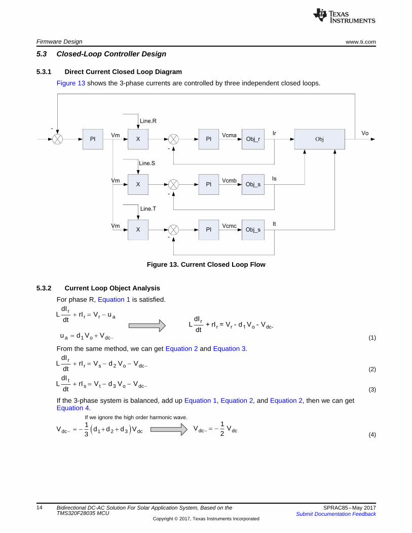
5.3.1 Direct Current Closed Loop DiagramFigure 13 shows the 3-phase currents are controlled by three independent closed loops.
Figure 13. Current Closed Loop Flow
5.3.2 Current Loop Object AnalysisFor phase R, Equation 1 is satisfied.
(1)
From the same method, we can get Equation 2 and Equation 3.
(2)
(3)
If the 3-phase system is balanced, add up Equation 1, Equation 2, and Equation 2, then we can getEquation 4.
If we ignore the high order harmonic wave.
(4)
www.ti.com Firmware Design
15SPRAC85–May 2017Submit Documentation Feedback
Copyright © 2017, Texas Instruments Incorporated
Bidirectional DC-AC Solution For Solar Application System, Based on theTMS320F28035 MCU
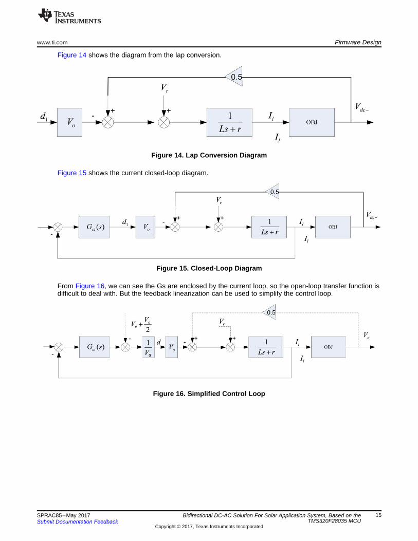
Figure 14 shows the diagram from the lap conversion.
Figure 14. Lap Conversion Diagram
Figure 15 shows the current closed-loop diagram.
Figure 15. Closed-Loop Diagram
From Figure 16, we can see the Gs are enclosed by the current loop, so the open-loop transfer function isdifficult to deal with. But the feedback linearization can be used to simplify the control loop.
Figure 16. Simplified Control Loop

cvK(s a)
G (s)s(s b)
�
�
1 2c _ 0 c _1 c _ 2
ci 1 2c _ 0 c _1
a a z a zG (z)
1 b z b z
� �
� �
� �
� �
ciK(s a)
G (s)s(s b)
�
�
Firmware Design www.ti.com
16 SPRAC85–May 2017Submit Documentation Feedback
Copyright © 2017, Texas Instruments Incorporated
Bidirectional DC-AC Solution For Solar Application System, Based on theTMS320F28035 MCU
5.3.3 Current and Voltage Loop ControllerFrom the previous analysis, we can select the current closed loop controller and plot the Bode figure forthe internal loop to fine tune the parameter effect (see Figure 17).
Figure 17. Current Loop Controller Analysis
Equation 5 shows the controller chosen as the voltage loops control, because the system has a largestorage capacitor so the BUS voltage changes very slowly. We could fine tune the parameter for thevoltage controller by experience.
(5)
5.4 DC-DC Controller With MPPT Feature
5.4.1 PV Panel Character AnalyzeFigure 18 shows the V-I curves for the solar cell.
Figure 18. V-I Curves for Solar Cell

www.ti.com Firmware Design
17SPRAC85–May 2017Submit Documentation Feedback
Copyright © 2017, Texas Instruments Incorporated
Bidirectional DC-AC Solution For Solar Application System, Based on theTMS320F28035 MCU
It is clear from the Figure 18 V versus I curve that PV does not have a linear voltage and currentrelationship. Thus the (P versus V) curve clearly shows a presence of a maximum. To get the most energyand use out of the PV system installation, it must be operated at the maximum power point of this curve.The maximum power point, however, is not fixed due to the nonlinear nature of the PV –cell and changeswith temperature, light, intensity, and so on, and varies from panel to panel. Therefore different techniquesare used to locate this maximum power point of the panel like Perturb and Observe, incrementalconductance. MPPT algorithm is used to track the MPP.
5.4.2 DC-DC Controller Loop DiagramFigure 19 shows the DC-DC interleaved boost converter control loops. This scenario uses current modecontrol. However, the goal is to control the PV panel output (Vpv), which is the input to the DC-DC stage.This allows the PV panel (array) to always operate at its maximum power point. Input current is regulatedby adjusting the duty cycles of the power switches. Input voltage is regulated by adjusting the inputcurrent. A MPPT algorithm described in the Section 5.4.3 is responsible for determining the set point(Vpv_ref) for the PV panel voltage.
The input voltage control loop works quite differently compared to conventional feedback used in outputvoltage control. Under this control scheme, when the PV panel voltage (Vpv) tends to go higher than thereference panel voltage (Vpv_ref) set by the MPPT algorithm, the control loop increases the panel currentcommand (reference current for inner current loop (Iind_ref) and thereby controls the panel voltage at itsreference level (Vpv_ref). When the panel voltage tends to go lower than the reference, the control loopreduces the panel current command to reestablish the panel voltage to its reference level.
Figure 19. DC-DC Control Loop Diagram

Firmware Design www.ti.com
18 SPRAC85–May 2017Submit Documentation Feedback
Copyright © 2017, Texas Instruments Incorporated
Bidirectional DC-AC Solution For Solar Application System, Based on theTMS320F28035 MCU
5.4.3 MPPT Algorithm Analyze and DesignTracking for the maximum power point is an essential part of PV system implementation. Several MPPTmethods have been implemented and documented for PV systems. This software module implements avery widely used MPPT method called the Perturb and Observe (P&O) algorithm. MPPT is achieved byregulating the panel voltage at the desired reference value. This reference is commanded by the MPPTP&O algorithm. The P&O algorithm continue to increment and decrement the panel voltage to observepower drawn change. First, a perturbation to the panel reference is applied in one direction and power isobserved. If the power increases, the same direction is chosen for the next perturbation, whereas if powerdecreases, the perturbation direction is reversed.
This module expects the following inputs:• Panel voltage (Vpv): Sensed panel voltage signal sampled by the ADC. The ADC result is converted to
per unit format.• Panel current (Ipv): Sensed panel current signal sampled by the ADC. The ADC result is converted to
per unit format.• Step size (Stepsize): Size of the step used to change the MPP voltage reference output; direction of
change is determined by the slope calculation done in the MPPT algorithm.
Upon macro call, Panel power (P(k) = V(k)*I(k)) is calculated, and compared with the panel powerobtained on the previous macro call. The direction of change in power determines the action on thevoltage output reference generated. If the current panel power is greater than the previous power voltagereference, it is moved in the same direction, as earlier. If not, the voltage reference is moved in theopposite direction.
Figure 20. MPPT Algorithm Flow

www.ti.com Firmware Design
19SPRAC85–May 2017Submit Documentation Feedback
Copyright © 2017, Texas Instruments Incorporated
Bidirectional DC-AC Solution For Solar Application System, Based on theTMS320F28035 MCU
5.5 Common Failure and Protection Mode
5.5.1 OvercurrentWhen the current across the low-arm shunt resistor reaches a certain threshold level, the overcurrentprotection circuit prevents damage to the inverter system by shutting down the PWM switching outputs ofthe control IC. When verifying new hardware, the overcurrent protection circuit should be tested early inthe process.
5.5.2 OvervoltageThe overvoltage fault is detected when the DC bus voltage reaches a certain threshold level. If anovervoltage fault is detected, the system prevents damage to the inverter system by shutting down thePWM switching output of the control IC. The fault states restore when the DC bus voltage returns tonormal range.
5.5.3 UndervoltageThe undervoltage fault is detected when the DC bus voltage falls beneath a certain threshold level. If anundervoltage fault is detected, the system prevents damage to the inverter system by shutting down thePWM switching output of the control IC. The fault states restore when the DC bus voltage returns tonormal range.
5.5.4 Anti-IslandingThe anti-islanding fault is detected when the voltage of the AC grid powers off. If an anti-islanding fault isdetected, the system prevents inverter independent output voltage from reaching the AC grid by shuttingdown the PWM switching output of the control IC. The fault states restore when the AC grid voltage turnson again.

Final Product Performance www.ti.com
20 SPRAC85–May 2017Submit Documentation Feedback
Copyright © 2017, Texas Instruments Incorporated
Bidirectional DC-AC Solution For Solar Application System, Based on theTMS320F28035 MCU
6 Final Product Performance
6.1 Running WaveformWhen the solar panel power is insufficient for running the air conditioning, the AC grid providescomplementary energy to air condition. The system runs in PFC mode, and the current and voltageremain in the same phase.
When there is an excess of solar panel power, the surplus energy feeds back to the AC grid. The systemruns in Inverter mode, and the current and voltage remains in 180c phase. These two modes aretranslated between each other automatically in real time.
Figure 21. Current and Voltage Waveform in PFC Mode

www.ti.com Final Product Performance
21SPRAC85–May 2017Submit Documentation Feedback
Copyright © 2017, Texas Instruments Incorporated
Bidirectional DC-AC Solution For Solar Application System, Based on theTMS320F28035 MCU
Figure 22. Current and Voltage Waveform in Translation Mode
Figure 23. Current and Voltage Waveform in Inverter Mode

Related Documentation www.ti.com
22 SPRAC85–May 2017Submit Documentation Feedback
Copyright © 2017, Texas Instruments Incorporated
Bidirectional DC-AC Solution For Solar Application System, Based on theTMS320F28035 MCU
7 Related Documentation1. Texas Instruments, TMS320F28030/28031/28032/28033/28034/28035 Piccolo Microcontrollers, Data
Sheet2. Texas Instruments, TMS320x2803x Piccolo System Control and Interrupts Reference Guide, Technical
Reference Manual3. Texas Instruments, UG_HV_SOLAR_DC_DC

IMPORTANT NOTICE FOR TI DESIGN INFORMATION AND RESOURCES
Texas Instruments Incorporated (‘TI”) technical, application or other design advice, services or information, including, but not limited to,reference designs and materials relating to evaluation modules, (collectively, “TI Resources”) are intended to assist designers who aredeveloping applications that incorporate TI products; by downloading, accessing or using any particular TI Resource in any way, you(individually or, if you are acting on behalf of a company, your company) agree to use it solely for this purpose and subject to the terms ofthis Notice.TI’s provision of TI Resources does not expand or otherwise alter TI’s applicable published warranties or warranty disclaimers for TIproducts, and no additional obligations or liabilities arise from TI providing such TI Resources. TI reserves the right to make corrections,enhancements, improvements and other changes to its TI Resources.You understand and agree that you remain responsible for using your independent analysis, evaluation and judgment in designing yourapplications and that you have full and exclusive responsibility to assure the safety of your applications and compliance of your applications(and of all TI products used in or for your applications) with all applicable regulations, laws and other applicable requirements. Yourepresent that, with respect to your applications, you have all the necessary expertise to create and implement safeguards that (1)anticipate dangerous consequences of failures, (2) monitor failures and their consequences, and (3) lessen the likelihood of failures thatmight cause harm and take appropriate actions. You agree that prior to using or distributing any applications that include TI products, youwill thoroughly test such applications and the functionality of such TI products as used in such applications. TI has not conducted anytesting other than that specifically described in the published documentation for a particular TI Resource.You are authorized to use, copy and modify any individual TI Resource only in connection with the development of applications that includethe TI product(s) identified in such TI Resource. NO OTHER LICENSE, EXPRESS OR IMPLIED, BY ESTOPPEL OR OTHERWISE TOANY OTHER TI INTELLECTUAL PROPERTY RIGHT, AND NO LICENSE TO ANY TECHNOLOGY OR INTELLECTUAL PROPERTYRIGHT OF TI OR ANY THIRD PARTY IS GRANTED HEREIN, including but not limited to any patent right, copyright, mask work right, orother intellectual property right relating to any combination, machine, or process in which TI products or services are used. Informationregarding or referencing third-party products or services does not constitute a license to use such products or services, or a warranty orendorsement thereof. Use of TI Resources may require a license from a third party under the patents or other intellectual property of thethird party, or a license from TI under the patents or other intellectual property of TI.TI RESOURCES ARE PROVIDED “AS IS” AND WITH ALL FAULTS. TI DISCLAIMS ALL OTHER WARRANTIES ORREPRESENTATIONS, EXPRESS OR IMPLIED, REGARDING TI RESOURCES OR USE THEREOF, INCLUDING BUT NOT LIMITED TOACCURACY OR COMPLETENESS, TITLE, ANY EPIDEMIC FAILURE WARRANTY AND ANY IMPLIED WARRANTIES OFMERCHANTABILITY, FITNESS FOR A PARTICULAR PURPOSE, AND NON-INFRINGEMENT OF ANY THIRD PARTY INTELLECTUALPROPERTY RIGHTS.TI SHALL NOT BE LIABLE FOR AND SHALL NOT DEFEND OR INDEMNIFY YOU AGAINST ANY CLAIM, INCLUDING BUT NOTLIMITED TO ANY INFRINGEMENT CLAIM THAT RELATES TO OR IS BASED ON ANY COMBINATION OF PRODUCTS EVEN IFDESCRIBED IN TI RESOURCES OR OTHERWISE. IN NO EVENT SHALL TI BE LIABLE FOR ANY ACTUAL, DIRECT, SPECIAL,COLLATERAL, INDIRECT, PUNITIVE, INCIDENTAL, CONSEQUENTIAL OR EXEMPLARY DAMAGES IN CONNECTION WITH ORARISING OUT OF TI RESOURCES OR USE THEREOF, AND REGARDLESS OF WHETHER TI HAS BEEN ADVISED OF THEPOSSIBILITY OF SUCH DAMAGES.You agree to fully indemnify TI and its representatives against any damages, costs, losses, and/or liabilities arising out of your non-compliance with the terms and provisions of this Notice.This Notice applies to TI Resources. Additional terms apply to the use and purchase of certain types of materials, TI products and services.These include; without limitation, TI’s standard terms for semiconductor products http://www.ti.com/sc/docs/stdterms.htm), evaluationmodules, and samples (http://www.ti.com/sc/docs/sampterms.htm).
Mailing Address: Texas Instruments, Post Office Box 655303, Dallas, Texas 75265Copyright © 2017, Texas Instruments Incorporated