Embed Size (px)
Citation preview
Bimodal substrate biasing to control γ-Al2O3 deposition during reactive magnetronsputteringMarina Prenzel, Annika Kortmann, Adrian Stein, Achim von Keudell, Farwah Nahif, and Jochen M. Schneider Citation: Journal of Applied Physics 114, 113301 (2013); doi: 10.1063/1.4819227 View online: http://dx.doi.org/10.1063/1.4819227 View Table of Contents: http://scitation.aip.org/content/aip/journal/jap/114/11?ver=pdfcov Published by the AIP Publishing Articles you may be interested in Carbon film deposition on SnO 2 / Si (111) using DC unbalanced magnetron sputtering AIP Conf. Proc. 1554, 93 (2013); 10.1063/1.4820292 Infrared optical properties of amorphous and nanocrystalline Ta2O5 thin films J. Appl. Phys. 114, 083515 (2013); 10.1063/1.4819325 A reactive magnetron sputtering route for attaining a controlled core-rim phase partitioning in Cu2O/CuO thinfilms with resistive switching potential J. Appl. Phys. 113, 183522 (2013); 10.1063/1.4804326 Metal versus rare-gas ion irradiation during Ti1− x Al x N film growth by hybrid high power pulsed magnetron/dcmagnetron co-sputtering using synchronized pulsed substrate bias J. Vac. Sci. Technol. A 30, 061504 (2012); 10.1116/1.4750485 Suppression of near-edge optical absorption band in sputter deposited Hf O 2 – Al 2 O 3 nanolaminatescontaining nonmonoclinic Hf O 2 Appl. Phys. Lett. 92, 141912 (2008); 10.1063/1.2907331
Reuse of AIP Publishing content is subject to the terms at: https://publishing.aip.org/authors/rights-and-permissions. Download to IP: 134.147.160.151 On: Mon, 18 Apr
2016 14:19:50
Bimodal substrate biasing to control c-Al2O3 deposition during reactivemagnetron sputtering
Marina Prenzel,1,a) Annika Kortmann,1 Adrian Stein,1 Achim von Keudell,1 Farwah Nahif,1
and Jochen M. Schneider2
1Research Group Reactive Plasmas, Ruhr-Universit€at Bochum, D-44801 Bochum, Germany2Materials Chemistry, RWTH Aachen University, D-52074 Aachen, Germany
(Received 22 May 2013; accepted 9 August 2013; published online 16 September 2013)
Al2O3 thin films have been deposited at substrate temperatures between 500 �C and 600 �C by
reactive magnetron sputtering using an additional arbitrary substrate bias to tailor the energy
distribution of the incident ions. The films were characterized by X-ray diffraction and Fourier
transform infrared spectroscopy. The film structure being amorphous, nanocrystalline, or
crystalline was correlated with characteristic ion energy distributions. The evolving crystalline
structure is connected with different levels of displacements per atom (dpa) in the growing film
as being derived from TRIM simulations. The boundary between the formation of crystalline
films and amorphous or nanocrystalline films was at 0.8 dpa for a substrate temperature of
500 �C. This threshold shifts to 0.6 dpa for films grown at 550 �C. VC 2013 AIP Publishing LLC.
[http://dx.doi.org/10.1063/1.4819227]
I. INTRODUCTION
Reactive magnetron sputtering (RMS) is a prominent
technique to deposit many thin film materials as, for exam-
ple, oxides and nitrides using metal targets and the addition
of oxygen and/or nitrogen as a reactive component to the ar-
gon plasma gas.1–4 The film stoichiometry and its structure
can be adjusted by controlling the energy impact of the film
forming growth flux.
In 2005, Ros�en et al. have reviewed phase formation
data reported for vapor phase deposited alumina5 and have
summarized that the majority of authors observe the crystal-
line growth temperature to be reduced as the mobility of sur-
face species through energetic ion bombardment is
increased. In 2010, Jiang et al. report on a-alumina forma-
tion temperature of 560 �C by utilizing large ion fluxes dur-
ing PACVD6 as discharge power densities of 19 W cm�2
resulted in an increase in the energy and the flux of the bom-
barding species towards the growing film, as well as in a
more efficient precursor dissociation.6 In the same year,
Sarakinos et al. reported an a-alumina formation temperature
of 720 �C by cathodic arc deposition7 for substrate bias
potentials between �40 V and –200 V. Based on ab initiomolecular dynamics calculations,8 sub-plantation of the im-
pinging Al is identified to cause significantly larger irradia-
tion damage and hence larger mobility in the c-alumina as
compared with a-alumina. Consequently, the enhanced mo-
bility results in the growth of the a phase at the expense of
the c phase.
It can be concluded that besides ion bombardment medi-
ated surface diffusion, sub-plantation mechanisms7,8 contrib-
ute to the formation of crystalline alumina thin films. Ion
bombardment of a film surface can be characterized by the
mean energy per incorporated atom hEi. Adibi et al.9 and
Petrov et al.10 showed that under variation of the average pa-
rameter hEi and the ion to neutral ratio jions=jgrowth, the aver-
age energy per incorporated atom hEi is no universal
parameter for the formation of titanium nitride (Ti0.5Al0.5N).
However, in addition to Musil et al.,11 the average energy
per incorporated atom is suggested to define the formation of
crystallinity by several authors.12–14
Bedra et al.15 defined three contributions to the energetic
growth flux, namely, collisional impact, condensation
energy, and electromagnetic radiation. Collisional impact is
defined as the impact of neutral particles, ions, and electrons
to the film surface. All incorporated species are expressed as
growth flux jgrowth consisting of aluminum and oxygen
atoms. Energetic neutrals may also be produced from the
reflection of ions at the target, which neutralize in the bulk
plasma. Finally, all energetic ions contribute to the energy
impact to the growing film through collisions depending on
the sheath potential in front of the substrate which can be
modified by a bias voltage. The energy impact of the ions is
determined by the ion energy distribution function (IEDF).
Incident ions may enhance the adatom mobility and promote
thereby crystallinity and/or a certain crystalline orienta-
tion.3,5,16 The energy impact to the film surface through ion
bombardment is quantified by the number of displacement
per atoms in the film.
Recently, we devised an experiment to very accurately
control the growth flux and the energy distribution of the
incident ions17 by keeping the average energy per deposited
atom hEi, the average energy of the incident ions Eions, the
total ion flux jions, and the ion-to-neutral ratio jions=jgrowth
constant, but changing only the IED, for details, see Ref. 17.
We applied this concept to RMS of Al2O3 films as a promi-
nent material with applications ranging from microelec-
tronics, wear resistant coatings to catalytic surfaces.4 The
most common phases of Al2O3 are the c and a phase. a-
Al2O3 with its hexagonal closed package (hcp)18 structure isa)Electronic mail: [email protected]
0021-8979/2013/114(11)/113301/7/$30.00 VC 2013 AIP Publishing LLC114, 113301-1
JOURNAL OF APPLIED PHYSICS 114, 113301 (2013)
Reuse of AIP Publishing content is subject to the terms at: https://publishing.aip.org/authors/rights-and-permissions. Download to IP: 134.147.160.151 On: Mon, 18 Apr
2016 14:19:50
often used as hard coating on machining tools. In this paper,
the impact of energetic ions to the crystal film evolution is
tested. This is often quantified by the energy per deposited
atom hEi. This energy depends on the ion energy Eions and
on the ion-to-neutral ratio jions/jgrowth in the growth flux with
hEi ¼ Eions � jions=jgrowth. Here, jions is the flux of incident
ions and jgrowth the flux of incorporated atoms in the film.
In our experiments, the energy of the growth flux is
dominated by the ion bombardment as discussed in the fol-
lowing: all deposition processes are performed at constant
pressure and rf power, so that the energy impact through
electromagnetic radiation (which might be changed through
an increase in pressure or rf power) remains at a constant
level.19 No influence of electromagnetic radiation to the
crystal evolution of the thin films is expected. The condensa-
tion energy for aluminum and oxygen atoms is equal to the
surface binding energies of both species (5.45 eV for Al and
7.01 eV for O (Ref. 20)). This is not regarded to discuss the
transition in crystalline phases, because the condensation
energy is always dissipated during film formation from ele-
ments. The amount of fast reflected neutrals is estimated
from TRIM simulations, determining the amount of back-
scattered particles when bombarding the Al2O3 target with
of Al or O ions with energies of 500 eV. The backscattered
ions are only 2.9% of the incident Al and O ion flux. This
has to be compared to the growth flux jgrowth. Since the ioni-
zation degree is only in the percent range and only a percent
of those ions may reach the substrate as backscattered neu-
trals, this contribution to the growth flux is of the order of
10�4. We neglect this contribution.
Previously,17 we monitored the transition from X-ray
amorphous to c-alumina to assess the influence of the ion
energy distribution on thin film growth, indicating that typi-
cally one displacement per incorporated atom (dpa) is neces-
sary for that transition to occur. In this paper, we expand the
data set and measured a comprehensive set of X-ray diffrac-
tion (XRD) and Fourier transform infrared spectroscopy
(FTIR) data to also identify nanocrystalline samples, which
appear as being crystalline in the FTIR measurement
although they are still X-ray amorphous. Based on this large
data set, the hypothesis of characteristic dpa levels to allow
for a certain structural transitions in the films can be more
thoroughly tested. Formation of amorphous films, of nano-
crystalline films, or of X-ray c-crystalline Al2O3 films was
observed by FTIR and XRD. It has to be emphasized that
our parameter interval is restricted to only the variation of
the ion energy distribution function of the incoming ions and
the substrate temperature. Therefore, it is possible to isolate
the effect of the transfer of kinetic energy on the film
growth.
II. EXPERIMENTAL METHODS
A. Film deposition
Thin aluminum oxide films were deposited using a dual
frequency magnetron sputter experiment employing
13.56 MHz and 71 MHz for plasma generation, as described
in detail in Ref. 17. The discharge was operated at 0.1 Pa at a
constant argon flow rate of 9 sccm. The base pressure in the
deposition chamber was 2 � 10�5 Pa. Based on Refs. 17 and
21, this is expected to lead to H incorporation of <2 at. %.
The incorporated H atoms from water in the residual gas22
are small enough that the effect of incorporated water in the
films can be neglected. A feedback loop regulated the oxy-
gen flow into the chamber to avoid target poisoning by moni-
toring a constant intensity of the Al I emission line at
396.2 nm using a narrow band pass filter and a photomulti-
plier. The adjusted oxygen partial pressure in the deposition
chamber was determined as 8:6 � 10�3 Pa in average.
Thereby, stoichiometric Al2O3 coatings were prepared as
being verified by ex situ X-ray Photoelectron Spectroscopy
(XPS).
The distance between target and the p-doped Si(100)
substrate was 50 mm. The substrate temperature during the
deposition process was regulated to 500 �C, 550 �C, and
600 �C, respectively. The substrate temperature was directly
measured by analyzing the temperature dependent refraction
index of silicon at 632.8 nm by ellipsometry.23 This is non-
intrusive and measures directly the surface temperature. Any
thermocouple at the substrate holder may read a different
temperature due to improper thermal contacts. Pyrometry
remains ambiguous because the emissivity of the coated sili-
con wafer is not well defined and silicon becomes transpar-
ent in the infrared wavelength range at high temperatures.
B. Substrate biasing and ion energy distribution
The substrate electrode was intentionally biased to tailor
the IEDF of the incident ions. Rectangular waveforms were
generated by a waveform generator and amplified using a
broadband amplifier. A coupling capacitor was used to con-
nect the biasing signal to the substrate electrode.
The kinetic energy of the impinging ions is controlled as
follows: a rectangular biasing signal can be divided into an
on-time (son) and an off-time (sof f ). The frequency of the
pulsing f is given as f ¼ 1=ðson þ sof f Þ. In our experiments,
the on-time son was fixed to a value of 500 ns and a change
in frequency f of the applied biasing signal was realized by
changing the off-time sof f only. Thereby, the fluence
(¼ jionsson) of energetic ions during growth remains identical
in all experiments. The maximum ion energy Eions;max, in
case of collisionless sheaths, corresponds to the voltage drop
between the biasing signal Umax and the plasma potential.
Consequently, Eions;max was used as parameter to uniquely
characterize the ion bombardment during film growth.
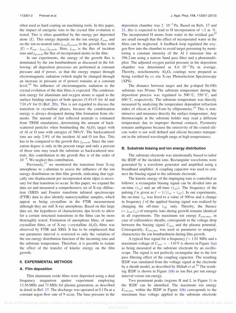
A typical bias signal for a frequency f¼ 1.01 MHz and a
maximum voltage of Umax ¼ �110 V is shown in Figure 1(a)
as being measured at the substrate electrode by an oscillo-
scope. The signal is not perfectly rectangular due to the low
pass filtering effect of the coupling capacitor. The resulting
IEDF was simulated from the voltage signal at the electrode
by a sheath model, as described by Shihab et al.24 The result-
ing IEDF is shown in Figure 1(b) as ion flux per ion energy
interval versus ion energy.
Two prominent peaks (regions H and L in Figure 1) in
the IEDF can be identified. The maximum ion energy
Eions;max within the IEDF in Figure 1(b) corresponds to the
maximum bias voltage applied to the substrate electrode
113301-2 Prenzel et al. J. Appl. Phys. 114, 113301 (2013)
Reuse of AIP Publishing content is subject to the terms at: https://publishing.aip.org/authors/rights-and-permissions. Download to IP: 134.147.160.151 On: Mon, 18 Apr
2016 14:19:50
Umax (region H). During this time period, ions are acceler-
ated by the voltage drop between plasma potential (18 V)
and maximum bias voltage to the substrate electrode (Umax).
This results in a maximum ion energy of Eions;max
¼ 18 eV � Umax � e. In addition, a low energetic peak (region
L) originates from ions accelerated during the off-time sof f
with an ion energy corresponding to the voltage drop
between plasma potential and floating potential.
Frequencies f between 0.80 MHz and 1.60 MHz were
applied to regulate the ratio between the ion flux at high
vs. low ion energies. The ion energy of the high energetic
peak within the IEDF was adjusted to a desired ion energy
by a defined tailoring of the maximum bias voltage Umax.
Therefore, any ratio between the two peaks within the
IEDF and any position of the high energetic peak can be
reached by tailoring frequency f and maximum bias voltage
Umax.
The energy impact during film growth is usually defined
by the mean energy per incorporated atom hEi depending
on the maximum ion energy of the ions Eions;max, the
total growth flux jgrowth, the ion flux jions, and the duty cycle
d:c: ¼ son � f according to
hEi ¼ Eions;max �jions
jgrowth� son � f : (1)
The growth flux jgrowth is defined by the incorporated flux
of aluminum and oxygen atoms during Al2O3 film formation.
This is deduced from the total film thickness, as measured exsitu by a profilometer, divided by the overall deposition time.
The growth rate g expressed in nm s�1 is converted into the
growth flux in cm�2 s�1 using the density of the film q and
the mass M of Al2O3 via jgrowth ¼ g�qM . Suggesting that the final
film composition is equal to the incoming particle fluxes, the
mass of Al2O3 is calculated by the stoichiometric weight of
aluminum (MAl¼ 27 amu) and oxygen (MO¼ 16 amu) atoms
relating to MAl2O3¼ 0:4 �MAl þ 0:6 �MO. A residual thick-
ness inhomogeneity of 4% is observed which converts into an
error of the growth flux of 5%.
Because XRD analysis of our films exhibits good crys-
talline quality of c-alumina (see below), the film density
value from literature of q¼ 3.66 g cm�3 as being reported by
Levin and Brandon25 seems to have reasonable good agree-
ment with our films and is taken for the further discussion.
Finally, the ion flux to the substrate surface is required
when determining the mean ion energy per incorporated
atom hEi. The ion flux jions was measured using a retarding
field analyzer within a previous work.17 It was determined as
jions ¼ 13:5 � 1018 m�2s�1.
C. Thin film analysis
Phase formation was studied by XRD with a Bruker D8
General Area Diffraction System (GADDS) on the deposited
Al2O3 thin films. The incident angle of the beam was 15�
and the analyzed 2H angle range was 20� to 75�. The applied
voltage and current settings were 40 kV and 40 mA, respec-
tively. Three different peaks which can be associated to the cphase of Al2O3 are identified in the diffraction patterns of
our samples. The (311) direction can be found within the
XRD pattern at an angle of 37.30�. Moreover, peaks at
45.86� and 67.03� are identified as (400) and (440) orienta-
tions, respectively. Peak positions agree with the JCDPS file
No. 10-0425 for c-Al2O3 at 45.9� and 67.0�.Further analysis of the Al2O3 samples was realized by
ex situ FTIR transmission measurements using a Bruker IFS
66/S spectrometer. A polarizer was placed in front of the
sample, so that only s polarized light reached the sample.
The angle of incidence normal to the surface was 60�.Measurements were performed in the wavenumber range
between 400 cm�1 and 6000 cm�1. Background spectra of
non-coated silicon wafers were used.
Br€uesch et al.26 investigated FTIR spectra of amorphous
and c-aluminum oxide. The evolution of a sharp peak (or dip
within transmission spectra) at 950 cm�1 is characteristic for
c-Al2O3. Further broad oscillations at lower wavenumbers
being characterized by Chu et al.29 at 357 cm�1, 536 cm�1,
and 744 cm�1 were identified.
XRD and FTIR assess the crystallinity of the samples on
distinct length scales: (i) in XRD, the coherent scattering of
the incident X-radiation from a crystal leads to pronounced
peaks in the XRD diffractogram. In case of nanocrystalline
FIG. 1. (a) Rectangular biasing signal at the substrate electrode at 1.01 MHz, as measured by the oscilloscope. (b) Simulated ion energy distribution function
IEDF for the given bias signal by the model from Shihab et al.24 L and H indicate the low and high energy part of the IEDF, respectively.
113301-3 Prenzel et al. J. Appl. Phys. 114, 113301 (2013)
Reuse of AIP Publishing content is subject to the terms at: https://publishing.aip.org/authors/rights-and-permissions. Download to IP: 134.147.160.151 On: Mon, 18 Apr
2016 14:19:50
samples, significant line broadening occurs, which compli-
cates the evaluation of X-ray profiles. As a consequence, the
distinction between crystalline and amorphous samples
depends on the employed diagnostic method and nanocrys-
talline samples may not be detected by XRD. (ii) In FTIR,
the signal originates from the absorption of single Al-O
bonds at a frequency depending on the configuration of the
next neighbors. If nanocrystallites are formed, characteristic
LO or TO phonon peaks may appear in the infrared spec-
trum, whereas the coherent overlap of the scattered light in
XRD by crystalline region and amorphous sites may still
show X-ray amorphous diffraction patterns. The crystalline
size determination by XRD from line broadening can be
meaningfully employed for domain sizes of 2.5 nm to
200 nm.27 Hence, a domain size of 2.5 nm constitutes the
minimum size to be detected by XRD. FTIR measurements
are not sensitive to the domain size but appear to exhibit a
larger sensitivity as crystallinity probe than XRD.
Determining the Full Width at Half Maximum (FWHM)
of the (440) diffraction peak and using the Debye-Sherer
equation, grain sizes between 7 nm and 12 nm are deter-
mined for the deposited samples. No dependence between
domain size and ion energy could be identified. According to
McHale et al.28 and Ros�en et al.,5 the c phase is thermody-
namically stable compared with the a phase for grain sizes
smaller than 12 nm.
Based on the different measurement principles of XRD
and FTIR, the transition from amorphous, nanocrystalline, to
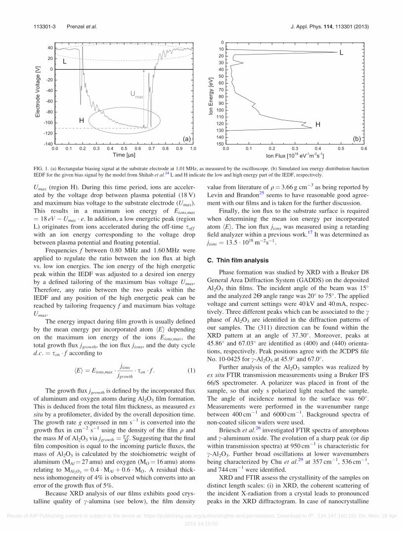
crystalline samples can be assessed, as illustrated in Figure 2
for films deposited at different deposition conditions, as
described below: (i) Figure 2 show the spectra for amor-
phous films, since no distinct peaks in the XRD diffracto-
gram (a) and no sharp absorption for TO phonon at
approximately 950 cm�1 is found (b); (ii) Figure 2 shows an
XRD diffractogram (c) for a nanocrystalline film, which
appears XRD-amorphous. Infrared absorption at a wavenum-
ber of 950 cm�1 reflects the formation of nanocrystallites,
which is shown in Figure 2(d); (iii) Figure 2 shows an XRD
diffractogram (e) for a crystalline film with sharp peaks in
the XRD diffractogram at position characteristic to c-
alumina. In addition to the XRD signature, pronounced
absorptions for TO phonon become also visible in the IR
spectrum (f). It is important to note that the identification of
the nanocrystalline phase from a comparison of the XRD
FIG. 2. Typical XRD- and FTIR-
spectra for amorphous samples ((a)
and (b)), for nanocrystalline samples
((c) and (d)), and for crystalline sam-
ples ((e) and (f)).
113301-4 Prenzel et al. J. Appl. Phys. 114, 113301 (2013)
Reuse of AIP Publishing content is subject to the terms at: https://publishing.aip.org/authors/rights-and-permissions. Download to IP: 134.147.160.151 On: Mon, 18 Apr
2016 14:19:50
and FTIR data remains ambiguous for very few cases,
because the sharpness of the TO-phonon peak in FTIR is not
as distinct as the analysis of the diffraction peaks in the XRD
diffractogram.
III. RESULTS AND DISCUSSION
A large set of 73 samples was prepared in the substrate
temperature range between 500 �C and 600 �C at a pressure
of 0.1 Pa. The IEDF was tailored using frequencies f in the
range between 0.80 MHz and 1.60 MHz for the pulsed bias
and maximum bias voltages between �25 V and �280 V.
The range of operating parameters and the resulting average
energies hEi are listed in Table I. The samples were analyzed
ex situ by XRD and FTIR with respect to their structure. The
deposition is characterized by the maximum ion energy
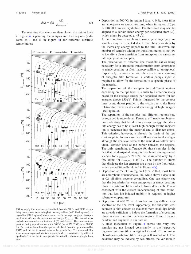
Eions;max and the average energy per incorporated atom hEi.Figure 4 shows the results for the amorphous samples (open
triangle), the nanocrystalline samples (half filled squares),
and the crystalline samples (solid squares) for three different
substrate temperatures of 500 �C (Figure 4(a)), of 550 �C(Figure 4(b)), and of 600 �C (Figure 4(c)). The dashed areas
in Figure 4 indicate deposition parameters, which are not
reasonable because the average energy hEi cannot be larger
than the maximum energy Eions;max.
Finally, the correlation of the deposition parameters
with the structure of the deposited films may be affected by
nucleation phenomena.
The data in Figure 4 indicate that crystalline films are
usually obtained if the average energy hEi and the maximum
energy Eions;max are above a certain threshold. This becomes
more critical at lower substrate temperatures, where also
amorphous films are observed at low hEi and Eions;max. The
films at intermediate values for hEi and Eions;max show nano-
crystalline behavior. At a temperature of 600 �C, aluminum
oxide is deposited in the c phase even for very low ion bom-
bardment and only very few samples remain amorphous.
This rough analysis already illustrates that an increasing
energy input during film growth induces a transition of the
film structure from an amorphous to a nanocrystalline and
finally to a crystalline structure. This is in agreement with the
current general understanding of energetic film deposition.
The ion-induced formation of a nanometer size crystal
or the c phase could be induced by displacement events
within a collision cascade. These displacements generate
mobility and may turn enable the formation of a crystalline
structure. This very general picture can be tested with our
data by comparing the samples, as plotted in Figure 4, with
TRIM simulations30 to calculate the displacements per incor-
porated atoms in the growing films.
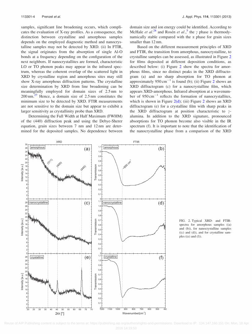
TRIM simulations were performed for argon ions, which
initiate a collision cascade in a stoichiometric Al2O3 film.
The surface binding energies were taken from Malherbe
et al. and are given as 5.45 eV for Al and 7.01 eV for O.20 A
density of 3.66 g cm�3 was assumed25 and mono energetic
argon ions with energies between 28 eV and 308 eV. This
corresponds to maximum voltages at the substrate electrode
Umax of �10 V to �300 V, respectively. The displacement
per ion (dpi) for the different ion energies was calculated and
plotted versus ion energy in Figure 3. No distinction between
displacing aluminum or oxygen was made. A threshold
energy of 25 eV for aluminum oxide is necessary to induce a
displacement event within the Al2O3 film. This value is equal
to the displacement energy of aluminum atoms in the Al2O3
thin film.30 Ion bombardment by a rectangular bias signal
establishes two distinct peaks with different ion energies im-
pinging onto the substrate surface. Ions with low energies
are below the threshold to initiate a displacement within the
aluminum oxide film. Only ions with ion energies above the
critical value of 28 eV have enough energy to initiate a dis-
placement within the film. The low energetic ions are accel-
erated within the off period of the bias signal, whereas high
energetic ions are produced during the on-time of the signal.
Therefore, only ions from the high energetic peak within the
IEDF account to the dpi within the Al2O3 films.
The displacements per ion (dpi) are converted into dis-
placements per atom (dpa) during film growth by multiply-
ing it with the ratio between energetic ion fluence per pulse
jionsson and the growth fluence jgrowthðson þ sof f Þ
dpa ¼ dpi � jions
jgrowth
ton
ton þ tof f¼ dpi � jions
jgrowthton � f : (2)
Equation (1) can be combined with Eq. (2) yielding a
dependence of the dpa level on the control parameters
Eions;max and hEi
TABLE I. Deposition parameters for Al2O3 growth by reactive magnetron
sputtering with an additional substrate bias.
Deposition/biasing parameter Adjusted values
Temperature T 500 �C, 550 �C, 600 �C
Biasing frequency f
0.80 MHz, 1.01 MHz, 1.20 MHz,
1.40 MHz, 1.60 MHz
Mean energy per incorporated atom hEi 10 eV–30 eV–60 eV
Maximum biasing voltage Umax �25 V–280 V
Maximum ion energy Eions;max 7 eV–262 eV
FIG. 3. TRIM calculation for dpi for Ar ions impinging onto an Al2O3
surface.
113301-5 Prenzel et al. J. Appl. Phys. 114, 113301 (2013)
Reuse of AIP Publishing content is subject to the terms at: https://publishing.aip.org/authors/rights-and-permissions. Download to IP: 134.147.160.151 On: Mon, 18 Apr
2016 14:19:50
dpa ¼ dpi � hEiEions;max
: (3)
The resulting dpa levels are then plotted as contour lines
in Figure 4, separating the samples into two regions (indi-
cated as I and II in Figure 4) for different substrate
temperatures:
• Deposition at 500 �C: in region I (dpa < 0.8), most films
are amorphous or nanocrystalline, while in region II (dpa
> 0.8) all films are crystalline. The threshold may also be
aligned to a certain mean energy per deposited atom hEi,which might be detected at 43 eV.
A transition from amorphous to nanocrystalline/crystalline
samples may be expected due to the phase evolution by
the increasing energy impact to the film. However, the
number of samples within the transition region is too low
to identify a clear transition from amorphous to nanocrys-
talline/crystalline samples.
The observation of different dpa threshold values being
necessary for a structural transformation from amorphous
to nanocrystalline or from nanocrystalline to amorphous,
respectively, is consistent with the current understanding
of energetic film formation: a certain energy input is
required to allow for the formation of a specific phase of
the material.
The separation of the samples into different regions
depending on the dpa level is similar to a criterion solely
based on the average energy per deposited atoms for ion
energies above 150 eV. This is illustrated by the contour
lines being almost parallel to the y-axis due to the linear
relationship between dpi and ion energy at high energies
(see Figure 3).
The separation of the samples into different regions may
be regarded in more detail. Petrov et al.9 made an observa-
tion indicating that besides an average energy, the abso-
lute energy has to be at least high enough for the incident
ion to penetrate into the material and to displace atoms.
This criterion, however, is already the basis of the dpa
contour plots. In our case, we still see structural changes
although the dpa level remains the same if we follow indi-
vidual contour lines at the border between the regions.
The only remaining difference for those samples is the
fact that the dissipated energy is distributed among several
species for Eions;max > 200 eV, but dissipated only by a
few atoms for Eions;max < 150 eV. The number of atoms
that dissipate the ion energies are given by the flux ratios,
which are additionally plotted in Figure 4(a).• Deposition at 550 �C: in region I (dpa < 0.6), most films
are amorphous or nanocrystalline, while above a dpa value
of 0.6 all films become crystalline. One can clearly see
that the boundaries between amorphous or nanocrystalline
films to crystalline films shifts to lower dpa levels. This is
consistent with the current understanding of film forma-
tion that less ion-induced mobility is required at higher
substrate temperatures.• Deposition at 600 �C: all films become crystalline, irre-
spective of the dpa level. Apparently, the substrate tem-
perature is high enough so that even very small dpa levels
are already sufficient to induce the formation of crystalline
films. A clear transition between regions II and I cannot
be identified anymore in our data set.
A close inspection of Figure 4 shows that very few
samples are not located consistently in the respective
region–crystalline films in region I instead of II, or amor-
phous/nanocrystalline films in region II instead of I. This
deviation may be induced by two effects, the variation in
FIG. 4. Al2O3 film structure as identified from the XRD- and FTIR spectra
being amorphous (open triangles), nanocrystalline (half filled squares), or
crystalline (filled squares) in dependence on the average energy per incorpo-
rated atom hEi and the maximum ion energy Eions;max. The shaded areas
exclude unreasonable combinations of hEi and Eions;max. The substrate tem-
perature during deposition was set at 500 �C (a), at 550 �C (b), or at 600 �C(c). The contour lines show the dpa, as calculated from the dpi simulated by
TRIM and the ion to neutral ratio in the growth flux. The measured film
structures are separated into two regions I and II, characterized by different
dpa levels. The ion flux to total growth flux ratio R is shown as straight lines
in (a).
113301-6 Prenzel et al. J. Appl. Phys. 114, 113301 (2013)
Reuse of AIP Publishing content is subject to the terms at: https://publishing.aip.org/authors/rights-and-permissions. Download to IP: 134.147.160.151 On: Mon, 18 Apr
2016 14:19:50
the nucleation process or the variation in the grain size
distribution:
(a) In nucleation a delicate competition between amor-
phous and crystalline phases can occur, where small
deviations in the initial condition such as substrate
morphology, contamination, etc. may lead to growth
of completely different film structures.
(b) The distinction between crystalline and amorphous
films by XRD depends very sensitive on the grain size
distribution. For small grains or low grain size density,
a crystalline phase might easily be undetected by
XRD. However, it should be emphasized that the vast
majority of samples can consistently be located in
regions I and II, respectively.
The mapping of the film structure on the parameters of
the energy input during film growth expressed in Eions;max
and hEi and its comparison to the dpa levels that are induced
during film growth shows good agreement. One may extrap-
olate this scaling to Al2O3 deposition in general, to predict
the film structure in the plasma based on the operating pa-
rameters of the system. The description of the IEDF with a
maximum ion energy is only reasonable for rectangular bias.
The underlying important quantity however is the dpa level
in the film, which can be uniquely calculated using TRIM
calculations for any ion energy distribution function. The
extrapolation of the proposed scaling approach for other bias
waveforms is currently under way.
IV. CONCLUSION
Al2O3 thin films have been deposited at substrate tem-
peratures between 500 �C and 600 �C by reactive magnetron
sputtering using an additional arbitrary substrate bias to tai-
lor the energy distribution of the incident ions. The forma-
tion of crystalline films as opposed to amorphous or
nanocrystalline films depends on a critical threshold of 0.8
displacement per incorporated atom at 500 �C substrate tem-
perature. This threshold shifts to 0.6 dpa with increasing sub-
strate temperature to 550 �C. One can conclude that for fixed
neutral to ion fluxes to the film surface, the dpa value is a
predictor for the formation of crystalline Al2O3 films. The
driving mechanism of the formation of crystalline structures
is the enhanced mobility of surface atoms due to Ar ion bom-
bardment. As the dpa value increases, the formation temper-
ature of crystalline Al2O3 thin films is decreased.
ACKNOWLEDGMENTS
The authors would like to thank Norbert Grabkowski for
his technical support within the experimental setup.
This project was supported by DFG (German Research
Foundation) within the framework of the Special Research
Field SFB-TR 87 and the Research Department “Plasmas
with Complex Interactions” at Ruhr-Universit€at Bochum.
Finally, the authors like to thank M. Shihab and R. P.
Brinkmann for their support in modeling the ion energy dis-
tribution functions for a given bias signal at the electrodes.
1K. Koski, J. H€ols€a, and P. Juliet, Thin Solid Films 339, 240 (1999).2P. J. Clarke, J. Vac. Sci. Technol. A 12, 594 (1994).3E. Wallin, T. I. Selinder, M. Elfwing, and U. Helmersson, EPL 82, 36002
(2008).4O. Zywitzki, G. Hoetzsch, F. Fietzke, and K. Goedicke, Surf. Coat.
Technol. 82, 169 (1996).5J. Ros�en, S. Mr�az, U. Kreissig, D. Music, and J. M. Schneider, Plasma
Chem. Plasma Process. 25, 303 (2005).6K. Jiang, K. Sarakinos, S. Konstantinidis, and J. M. Schneider, J. Phys. D:
Appl. Phys. 43, 325202 (2010).7K. Sarakinos, D. Music, F. Nahif, K. Jiang, A. Braun, C. Zilkens, and J.
M. Schneider, Phys. Status Solidi (RRL) 4, 154 (2010).8D. Music, F. Nahif, K. Sarakinos, N. Friederichsen, and J. M. Schneider,
Appl. Phys. Lett. 98, 111908 (2011).9F. Adibi, I. Petrov, J. E. Greene, L. Hultman, and J.-E. Sundgren, J. Appl.
Phys. 73, 8580 (1993).10I. Petrov, F. Adibi, J. E. Greene, L. Hultman, and J.-E. Sundgren, Appl.
Phys. Lett. 63, 36 (1993).11J. Musil, S. Kadlec, V. Valvoda, R. Ku�zel, and R. �Cern�y, Surf. Coat.
Technol. 43–44, 259 (1990).12V. Poulek, J. Musil, R. �Cern�y, and R. Kuzel, Thin Solid Films 170, L55
(1989).13V. Poulek, J. Musil, V. Valvoda, and R. Kuzel, Thin Solid Films 196, 265
(1991).14G. Grigorov, I. Martev, M. Stoyanova, J.-L. Vignes, and J.-P. Langeron,
Thin Solid Films 198, 169 (1991).15L. Bedra, A. L. Thomann, N. Semmar, R. Dussart, and J. Mathias, J. Phys.
D: Appl. Phys. 43, 065202 (2010).16J. Ros�en, J. M. Schneider, and K. Larsson, Solid State Commun. 135, 90
(2005).17M. Prenzel, A. Kortmann, A. von Keudell, F. Nahif, J. M. Schneider, M.
Shihab, and R. P. Brinkmann, J. Phys. D: Appl. Phys. 46, 084004 (2013).18M. Gautier, G. Fenaud, L. Pham Van, B. Villette, M. Pollak, N. Thromat,
F. Jollet, and J.-P. Duraud, J. Am. Ceram. Soc. 77, 323 (1994).19S. Bornholdt, T. Peter, T. Strunskus, V. Zaporojtchenko, F. Faupel, and H.
Kersten, Surf. Coat. Technol. 205, S388–S392 (2011).20J. B. Malherbe, S. Hofmann, and J. M. Sanz, Appl. Surf. Sci. 27, 355–365
(1986).21J. Ros�en, E. Widenkvist, K. Larsson, U. Kreissig, S. Mr�az, C. Martinez, D.
Music, and J. M. Schneider, Appl. Phys. Lett. 88, 191905 (2006).22J. M. Schneider, B. Hj€orvarsson, X. Wang, and L. Hultman, Appl. Phys.
Lett. 75, 3476 (1999).23G. M. W. Kroesen, G. S. Oehrlein, and T. D. Bestwick, J. Appl. Phys. 69,
3390 (1991).24M. Shihab, D. Ziegler, and R. P. Brinkmann, J. Phys. D: Appl. Phys. 45,
185202 (2012).25I. Levin and D. Brandon, J. Am. Ceram. Soc. 81, 1995 (1998).26P. Br€uesch, R. Koetz, H. Neff, and L. Pietronero, Phys. Rev. B 29, 4691
(1984).27C. S. Barrett and T. B. Massalski, Structure of Metals, 3rd ed. (Pergamon
Press, Oxford, New York, 1980), p. 654.28J. M. McHale, A. Auroux, A. J. Perrotta, and A. Navrotsky, Science 277,
788–791 (1997).29Y. T. Chu, J. B. Bates, C. W. White, and G. C. Farlow, J. Appl. Phys. 64,
3727 (1988).30W. M€oller and W. Eckstein, Nucl. Instrum. Methods Phys. Res. B 2, 814
(1984).
113301-7 Prenzel et al. J. Appl. Phys. 114, 113301 (2013)
Reuse of AIP Publishing content is subject to the terms at: https://publishing.aip.org/authors/rights-and-permissions. Download to IP: 134.147.160.151 On: Mon, 18 Apr
2016 14:19:50