Embed Size (px)
Citation preview

BJT Amplifier
• Two types analysis– DC analysis
• Applied DC voltage source– AC analysis
• Time varying signal source
• Superposition principle (linear amplifier)– The response of a linear amplifier circuit
excited by multiple independent input signalsis the sum of the responses of the circuit toeach of the input signals alone.

Variable MeaningiB, vBE Total instantaneous valuesIB, VBE DC valuesib,vbe Instantaneous ac valuesIb, Vbe Phasor values
Bipolar linear amplifier

Common Emitter with Time-Varying Input

IB versus VBECharacteristic
bBT
beBQB iI
VvIi +=+≅ )1(
( )1
22
%THDV
Vn∑∞
=
Total Harmonic Distortion (THD)

ac Equivalent Circuit for Common Emitter

Small-Signal Hybrid π Model for npn BJT
β
β
π
π
=
=
=
rgIVr
VI
g
m
CQ
T
T
CQm
Phasor signals are shown in parentheses.

Small-Signal Equivalent Circuit Using Common-Emitter Current Gain

Small-Signal Equivalent Circuit for npn Common Emitter circuit-voltage gain
))((B
Cmv RrrRgA+
−=π
π

• Calculate the small-signal voltage gain of the BJT asshown in figure. Assume the transistor and circuitparameters are β = 100, VCC =12 V, VBE = 0.7 V, RC =6 k Ω, RB = 50 kΩ, and VBB =1.2 V.

Problem-Solving Technique: BJT AC Analysis
1. Analyze circuit with only dc sources to find Q point.
2. Replace each element in circuit with small-signal model, including the hybrid π model for the transistor.
3. Analyze the small-signal equivalent circuit after setting dc source components to zero.

Hybrid π Model for npn with Early Effect
CQ
Ao I
Vr =
+=
A
CEVv
sc VveIi T
BE
1.
1
ptQCE
c
o vi
r−
∂∂
=
))(||(B
oCmv RrrrRgA+
−=π
π

Hybrid π Model for pnp with Early Effect
)||)((B
Comv Rr
RrrgA+
−=π
π

BJT Amplifier configurations
• Common emitter– Basic common emitter amplifier– With Emitter resistor– With bypass capacitor
• Common collector (emitter follower)• Common base
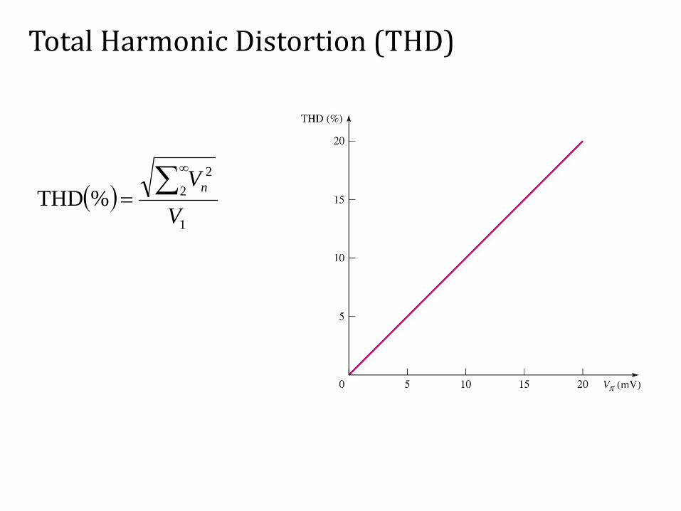
4 Equivalent 2-port Networks
Voltage Amplifier
Current Amplifier
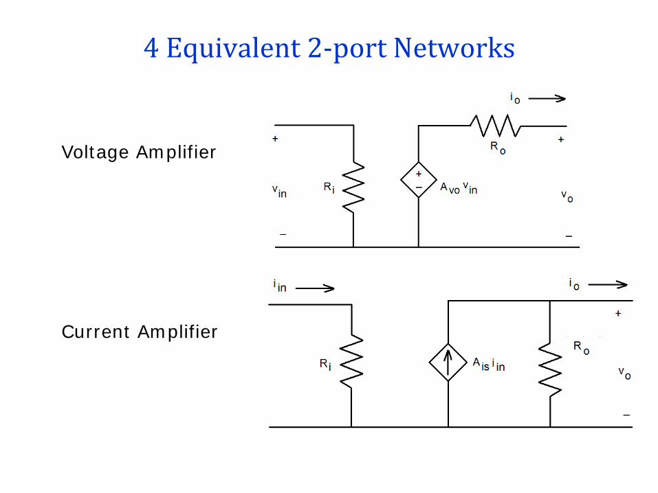
4 Equivalent 2-port Networks
Transconductance Amplifier
Transresistance Amplifier

Common Emitter with Voltage-Divider Bias and a Coupling Capacitor

Small-Signal Equivalent Circuit –Coupling Capacitor Assumed a Short

npn Common Emitter with Emitter Resistor
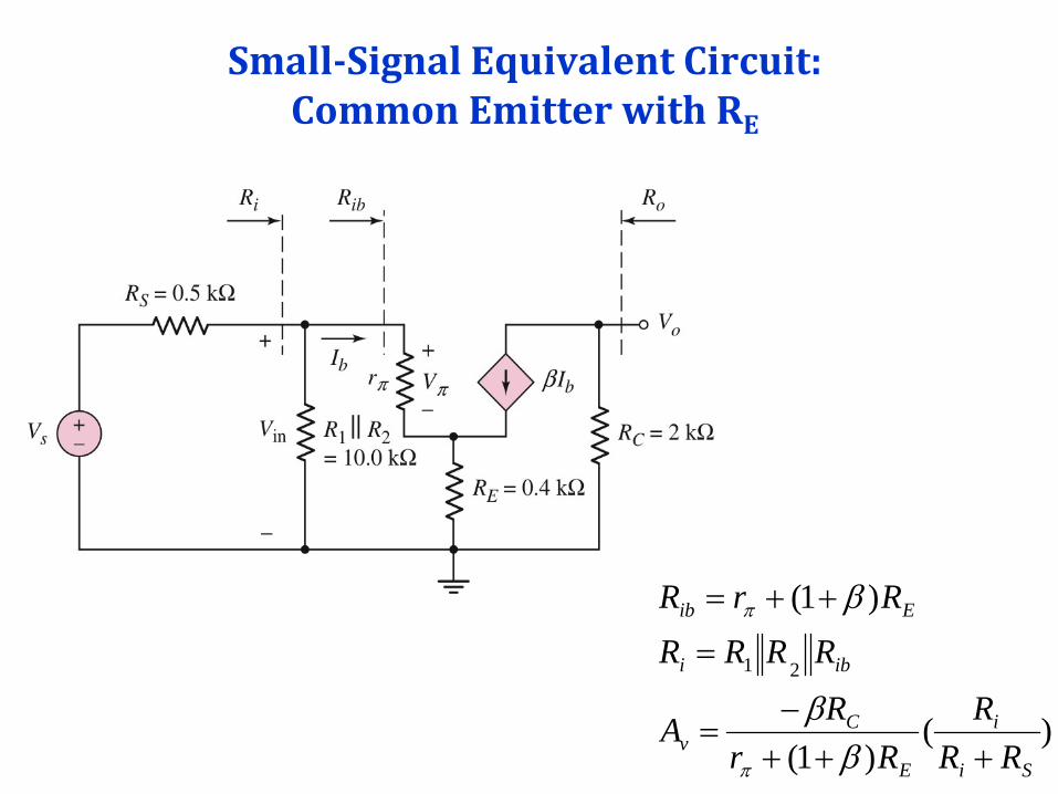
Small-Signal Equivalent Circuit:Common Emitter with RE
)()1(
)1(
21
Si
i
E
Cv
ibi
Eib
RRR
RrRA
RRRRRrR
+++−
=
=
++=
ββ
β
π
π

RE and Emitter Bypass Capacitor

Frequency Repsonse
Chapter 7 (Neamen Book)Sections 7.1-7.3.5

Operational Amplifier (Op Amp)• Amplifies the difference between two input signals
to give an output signal• 20-50 transistors
Ideal op-amp equivalent circuit


Equivalent circuit: Op-amp 741

Op-Amp
IdealInverting
Non-inverting
Applications
• T-network• Effect of finite gain• Summing amplifier • voltage follower
• current to voltage converter• voltage-to-current converter• difference amplifier• integrator & differentiator• precision half-wave rectifier

Small-Signal Equivalent Circuit:MOSFET with Input and Output Feedback
I
F
I
O
RR
vv
−=

Equivalent Circuit of Op-Amp
• Output voltage is limited: biased by dc voltages V+ and V-
• vo V+, it will saturate or limited to a value nearly equal to V+, similar for V-.• V- + ∆V <vo <V+-∆V

Inverting Op-Amp
Equivalent circuit

Inverting Op-Amp with T-Network
)1(2
3
4
3
1
2
RR
RR
RRAv ++−=
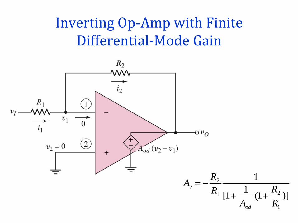
Inverting Op-Amp with Finite Differential-Mode Gain
)]1(11[
1
1
21
2
RR
ARRA
od
v
++−=

Field Effect Transistors (FET)
• Metal-Oxide Semiconductor FET (MOSFET)– n-type MOS– p-type MOS
• Junction FET (JFET)– pn junction FET

Basic MOS capacitor structure
MOSFET• Smaller in size• High density
VLSI• Based on field
enhancement• Modulation of
conductance ofsemiconductorsubstrate

p-typeUnderstanding the field enhancement

n-type
p-type substrate: +ve gate voltagen-type substrate: -ve gate voltage

n-channel enhancement mode MOSFET
• Channel length, L ~ 1 µm• Oxide length, tox ~ 400 Angstrom• NMOS (carriers are electrons)
p-type substrate, two n-regions (n-source, n-drain)Positive Gate voltage

Basic transistor operation
Cross-section of n-channel MOSFET prior to formation of electron inversion layer
Cross-section after theformation of electron inversion layer
Induced n-type channel
Depletion region

Threshold voltage VTN: applied gate voltage required to create an inversion charge in which the density is equal to the concentration of majority carriers in semiconductor substrate.
voltage at which the device turns ON
VGS < VTN, No currentVGS < VTN, current flow (drain to source)
Gate and drain voltages are measured with respect to source

• Thickness of inversion layer gives the relative charge density• VDS increases, the voltage drop across the oxide near the drain terminal
decreases– Decrease in induced charge density– Decrease in incremental conductance

• VDS increases to a point where the potential difference between gate and drain terminals (VGS-VDS) becomes equal to the threshold voltage
– Induced charge density at drain terminal becomes zero– Incremental conductance subsequently zero
VGS-VDS(sat)=VTN VDS(sat)=VGS-VTN

Family of curves
Ideal current-voltage characteristics

PMOS
n-type substrate, two p-regions (p-source, p-drain)Gate voltage ???, carriers ??

NMOS
PMOS
Circuit symbols

NMOS Common-Source Circuit
Variable Symbol meaningiD,vGS Total instantaneous values
ID,VGS DC values
id,vgs Instantaneous ac values
Id,Vgs Phasor values

NMOS Transistor Small-Signal Parameters
• Values depends on Q-point
112
1
][])([
)(
2)(2
−−
−∂∂
∂∂
≅−=
=
=−=
==
DQTNGSQno
vi
o
DQnTNGSQnm
gs
dvi
m
IVVKr
r
IKVVKg
vig
DS
D
GS
D
λλ
Transconductance (relates output current to input voltage)-can think as gain of a transistor

Simple NMOS Small-Signal Equivalent Circuit

NMOS Common-Source Circuit
AC Small-signal
)( Domiov RrgVVA −==
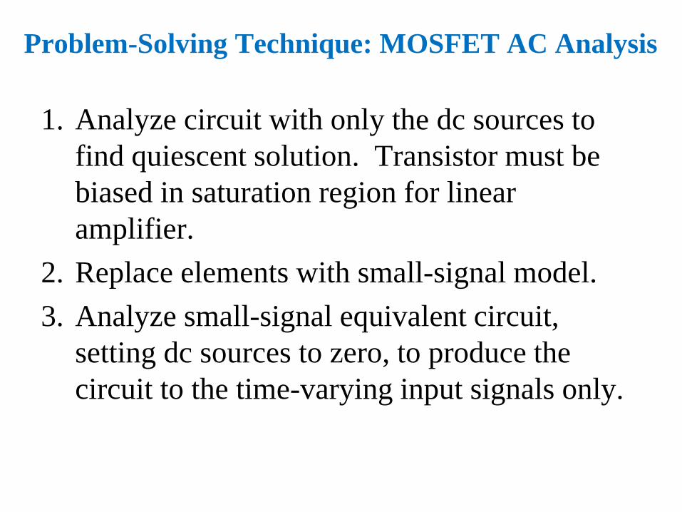
Problem-Solving Technique: MOSFET AC Analysis
1. Analyze circuit with only the dc sources to find quiescent solution. Transistor must be biased in saturation region for linear amplifier.
2. Replace elements with small-signal model.3. Analyze small-signal equivalent circuit,
setting dc sources to zero, to produce the circuit to the time-varying input signals only.

MOSFET Amplifier Configurations
Common sourceCommon drain (source follower)
Common gate
Input and output resistance characteristics are important in determining loading effects
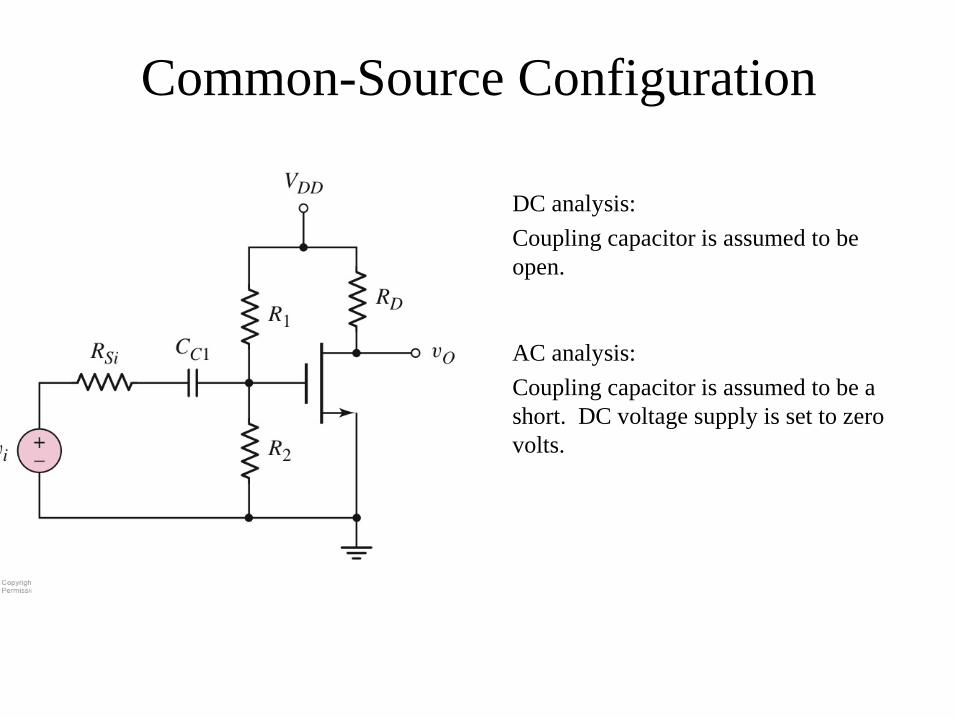
Common-Source Configuration
DC analysis: Coupling capacitor is assumed to be open.
AC analysis: Coupling capacitor is assumed to be a short. DC voltage supply is set to zero volts.

Small-Signal Equivalent Circuit
))((Sii
iDomiov RR
RRrgVVA+
−==
Output resistance can be calculated by setting the independent input source Vi =0 i.e. Vgs =0.
oDo rRR =

DC Load Line
Q-point near the middle of the saturation region for maximum symmetrical output voltage swing,.
Small AC input signal for output response to be linear.
Example
Determine the small-signal voltage gain and input and output resistances of acommon –source amplifier. For the circuit, the parameters are: VDD =10 V, R1=70.9kΩ, R2=29.1 kΩ, and RD=5 kΩ. The transistor parameters are VTN = 1.5 V, Kn=0.5mA/V2, and λ =0.01 V-1. Assume Rsi= 4 kΩ.

Common-Source Amplifier with Source Resistor
Source resistor is used to stabilize the Q-point against transistor parameter variation
- decreases the gain
Av = -5.76
Determine the small-signal voltage gainof a common-source circuit containing asource resistor. The transistor parametersare VTN = 0.8 V, Kn= 1 mA/V2, and λ =0.

Small-Signal Equivalent Circuitfor Common-Source with Source Resistor
Sm
Dmv Rg
RgA+−
=1
Dgsmo RVgV −=
Use of KVL from input around the gate-source loop
sgsmgsi RVgVV +=
sm
igs Rg
VV+
=1
If gm is very large, S
Dv R
RA −≅

Common-Source Amplifier with Bypass CapacitorSmall-signal equivalent circuit
To minimize the loss in small-signal voltage gain as in previousexample, while maintaining the Q-point stability, a bypasscapacitor can be added, or replacing the source resistor by aconstant current source.

Determine the small-signal voltage gain of a common-source circuit biased witha constant current source and incorporating a source bypass capacitor. Thetransistor parameters are VTN = 0.8 V, Kn= 1 mA/V2, and λ =0.