Embed Size (px)
Citation preview

© September 16, 2017 Dr. Lynn Fuller, Professor
Rochester Institute of Technology
Microelectronic Engineering
BJT IC Design
Page 1
ROCHESTER INSTITUTE OF TECHNOLOGYMICROELECTRONIC ENGINEERING
9-16-17 BJT_IC_Design.ppt
BJT IC Design
Dr. Lynn FullerWebpage: http://people.rit.edu/lffeee/
Microelectronic EngineeringRochester Institute of Technology
82 Lomb Memorial DriveRochester, NY 14623-5604
Tel (585) 475-2035
Email: [email protected] webpage: http://www.rit.edu/microelectronic/

© September 16, 2017 Dr. Lynn Fuller, Professor
Rochester Institute of Technology
Microelectronic Engineering
BJT IC Design
Page 2
OUTLINE
Differential Amplifier
Biasing, Current Sources, Mirrors
Output Stages
Operational Amplifiers
References
Homework Questions
© September 16, 2017 Dr. Lynn Fuller, Professor
Rochester Institute of Technology
Microelectronic Engineering
BJT IC Design
Page 3
DIFFERENTIAL AMPLIFIER
DC Analysis – assume:Identical transistors, Re=infinite, vin1=vin2=0
ThenIc1=Ic2=Ie/2Vo1=Vo2=Vcc-Rc Ie/2
Example: If Ie = 6mAVcc = 10, Vee = -10 and Rc = 2KAssume Vin1 = Vin2 = 0Vo1 = Vo2 = 4.0 voltsVE = -0.7VCE = 4.7
Rc
vi1
+
-
Rc
Re
vo1vi2
vo2+
-
+
-
+
-
Vee
Vcc
Ie
VE

© September 16, 2017 Dr. Lynn Fuller, Professor
Rochester Institute of Technology
Microelectronic Engineering
BJT IC Design
Page 4
SMALL SIGNAL ANALYSIS
rp
ib1
vi1
+
-
gm vbeor
b ib rp
ib2
vi2
+
-
Re
Rc Rc
vo2vo1
Lets define:
Differential input voltage
vid=vi1-vi2
Common input voltage
vic=(vi1+vi2)/2
Differential Output Voltage
Vod=Vo1-Vo2
Common output voltage
Voc=(Vo1+Vo2)/2
Single sided output voltage
Voss=Vo1 or Vo2
+Ve-

© September 16, 2017 Dr. Lynn Fuller, Professor
Rochester Institute of Technology
Microelectronic Engineering
BJT IC Design
Page 5
VOLTAGE GAINS: Avd, Avc, CMRR
Differential mode voltage gain, Avd = Vod / vid
Let vin1 = vid/2 + vic and vin2 = -vid/2 + vic
Ib1 = (vin1 – Ve) / rp Ib2 = (vin2 – Ve) / rp
Ib1 = (vid/2 – Ve) / rp Ib2 = (-vid/2 – Ve) / rp
Vo1 = - b ib1 Rc Vo2 = - b ib2 Rc
Vod = Vo1 – Vo2 = - b ib1 Rc - - b ib2 Rc
Vod = (b Rc / rp) (vid/2 +vid/2)
00
Avd = - b Rcrp
= - gm Rc

© September 16, 2017 Dr. Lynn Fuller, Professor
Rochester Institute of Technology
Microelectronic Engineering
BJT IC Design
Page 6
VOLTAGE GAINS: Avd, Avc, CMRR
Common Mode Voltage Gain Avc = Voc/Vic =(Vo1 + Vo2)/2(vin1 + vin2)/2
Let Vid = 0 thus vin1 = vin2 = Vic
Ve = 2 Re (b +1) ib
ib = (Vic – Ve) / rp
ib = Vic – 2 Re (b+1)ibrp 2 Re (b+1) + rp
Vic
- b ib1 Rc + -b ib2 Rc2
Voc =
- b Rc ib -b Rc Vic2Re (b+1) + rp
=Thus Voc =
and ib1 = ib2
-b Rc
2Re (b+1) + rpVoc Vic
=Avc =
Rearranging; ib =

© September 16, 2017 Dr. Lynn Fuller, Professor
Rochester Institute of Technology
Microelectronic Engineering
BJT IC Design
Page 7
OTHER RESULTS
Common Mode Rejection Ratio: CMRR is a figure of merit used to compare differential amplifiers
CMRR = AvdAvc
Differential Mode Input Resistance:
Rid = 2 rpCommon Mode Input Resistance:
Ric = rp + (b+1) 2 Re
Single Sided Output Differential Voltage Gain:
VossVid
=- b Rc
rp1/2
Single Sided Output Common Mode Voltage Gain:
-b Rc
2Re (b+1) + rpVoss Vic
= note: same
note: half

© September 16, 2017 Dr. Lynn Fuller, Professor
Rochester Institute of Technology
Microelectronic Engineering
BJT IC Design
Page 8
VARIATIONS
Variations:1. Resistor between emitter and –Vee rather than current source2. Series base resistors3. Emitter resistors4. Various types of current sources5. Darlington configuration6. FET’s7. Single sided outputs8. Active loads9. unbalanced or non symmetrical circuits

© September 16, 2017 Dr. Lynn Fuller, Professor
Rochester Institute of Technology
Microelectronic Engineering
BJT IC Design
Page 9
EXAMPLE DIFFERENTIAL AMPLIFIER
Analyze the following differential amplifier, b=200
2K
vi1
2K
vi2
vo2
+
-
+
-
-10
+10
T1 T21K1K

© September 16, 2017 Dr. Lynn Fuller, Professor
Rochester Institute of Technology
Microelectronic Engineering
BJT IC Design
Page 10
SOLUTION TO EXAMPLE ON PREVIOUS PAGE
DC Analysis:
Small Signal Analysis:Hand Calculation:
Avd = ½ gm Rc rpi/(1K+rpi)=62
or
Avd = ½ Beta Rc/(rpi +1K) = 62

© September 16, 2017 Dr. Lynn Fuller, Professor
Rochester Institute of Technology
Microelectronic Engineering
BJT IC Design
Page 11
SUMMARY
1. The differential amplifier should amplify the difference between
the two input voltages.
2. The differential amplifier should suppress signals that are
common to both inputs.
3. The differential amplifier with a constant current source is
superior to the differential amplifier with just a resistor.
4. The common mode rejection ratio is used as a figure of merit for
comparison.
5. The differential amplifier is a dc amplifier as well as an ac
amplifier.

© September 16, 2017 Dr. Lynn Fuller, Professor
Rochester Institute of Technology
Microelectronic Engineering
BJT IC Design
Page 12
709 OPERATIONAL AMPLIFIER

© September 16, 2017 Dr. Lynn Fuller, Professor
Rochester Institute of Technology
Microelectronic Engineering
BJT IC Design
Page 13
741 OPERATIONAL AMPLIFIER

© September 16, 2017 Dr. Lynn Fuller, Professor
Rochester Institute of Technology
Microelectronic Engineering
BJT IC Design
Page 14
SIMPLIFIED 741 OP AMP SCHEMATIC

© September 16, 2017 Dr. Lynn Fuller, Professor
Rochester Institute of Technology
Microelectronic Engineering
BJT IC Design
Page 15
SIMPLE CURRENT SOURCE
-V
Ie
+V
Load
Load
Ie
R
R
Ie = (V-0.7)/R
Ie Ree = roIn the next few pages we
will investigate current
sources, level shifting and
output stages of op amps

© September 16, 2017 Dr. Lynn Fuller, Professor
Rochester Institute of Technology
Microelectronic Engineering
BJT IC Design
Page 16
CURRENT SOURCE (HW Problem 1)
There are many types of current sources. Consider the following:
4.3K
-10
T15K
ReeIe
What is Ie? (Ans: 1mA)
5K
b ib
rpvbe+
-vtest
+
-
5K
4.3K
ib
5K
itest
ro
Ree = infinity if ro = infinite (not there)
Ree is calculated by students in pro.1.
Ree in this example is 4.68 Meg
if b = 100 and ro = 100K
rp = b(0.026/1mA)
= 100 (26)= 2.6K

© September 16, 2017 Dr. Lynn Fuller, Professor
Rochester Institute of Technology
Microelectronic Engineering
BJT IC Design
Page 17
CURRENT SOURCES
-V
IeLoad
I2I1Re
R1 Vbe1 = Vbe2 + I2Re
KT/q ln I1/Is = KT/q ln I2/Is + I2Re
note: I2 is always smaller than I1
Ie can be small without R1being small
Ree is ~Meg ohms
KT/q ln(I1/I2)= I2Re

© September 16, 2017 Dr. Lynn Fuller, Professor
Rochester Institute of Technology
Microelectronic Engineering
BJT IC Design
Page 18
EXAMPLES FOR CURRENT SOURCE
Example 1: suppose I1 = 1 mA and I2 is 10 uA find Re
Example 2: suppose I1 = 1 mA and Re = 20K find I2
KT/q ln(I1/I2)= I2Re
KT/q ln(I1/I2) = I2Re
0.026 ln (1mA/10uA) = 10uA Re
0.1197 = 10uA Re
Re = 11.97K
0.026ln(1mA/I2)=20KI2
Try I2 = Left Side =
1uA 179K
5uA 27.6K
6uA 22.2K
7uA 18.4K
Etc.

© September 16, 2017 Dr. Lynn Fuller, Professor
Rochester Institute of Technology
Microelectronic Engineering
BJT IC Design
Page 19
MORE CURRENT SOURCES
Figure 1. (a) Basic, (b) Current-buffered, and (c) Wilson current sources.
Io
IseqV B E / kT( )
1 VC E
VA
Io = Iref / (1+2/b) Io = Iref / (1+2/b2)Io = Iref / (1+2/b2)
Ree = ro Ree = ro Ree = MEG ohms

© September 16, 2017 Dr. Lynn Fuller, Professor
Rochester Institute of Technology
Microelectronic Engineering
BJT IC Design
Page 20
LEVEL SHIFTING
It would be nice to have zero volts out when we have zero volts in. We can achieve this by adding a level shifting stage.
DC Voltage
Level
Shifting
+
Vshift
-
I1
-10
Vo2
Vout
+10
If Ie = 6mA
And Rc = 2K
for vi1 = vi2 = 0
Vo2 = 4 volts
Thus we need a
4 volt shift to make
Vout = 0 volts
Rc
vi1
+
-
Rc
Re
vo1vi2
vo2+
-
+
-
+
-
Vee = -10
Vcc =+10
Ie
Vo1
Note: in the ac equivalent circuit current sources are open circuits and voltage sources are short circuit. (We could use a battery)

© September 16, 2017 Dr. Lynn Fuller, Professor
Rochester Institute of Technology
Microelectronic Engineering
BJT IC Design
Page 21
VOLTAGE SOURCES / REFERENCES
I1VL = nVbe
n
VL = Vz + Vbe
ro = n(KT/q)/I1 ro = rz + (KT/q)/I1
I1
dVL/dT = dVz/dT +dVbe/dT
Vz
Voltage sources should have constant voltage and zero source resistance.

© September 16, 2017 Dr. Lynn Fuller, Professor
Rochester Institute of Technology
Microelectronic Engineering
BJT IC Design
Page 22
VOLTAGE SOURCES
Load
+V
What is the purpose of D1?
(answer: reduces the change in VL with temperature)
D1
R2
R1
Assume Ib is small compared to I1
I1
VB -0.7 = (V-0.7) R2/(R1+R2)
VB
ro = rp + R1//R2
VL = VB - 0.7
Therefore: VL = (V-0.7) R2/(R1+R2)
(b+1)Note: small
VL+
-

© September 16, 2017 Dr. Lynn Fuller, Professor
Rochester Institute of Technology
Microelectronic Engineering
BJT IC Design
Page 23
VOLTAGE MIRROR
VzLoadLoad LoadLoad
+V+V
Vz
multiple emittertransistor

© September 16, 2017 Dr. Lynn Fuller, Professor
Rochester Institute of Technology
Microelectronic Engineering
BJT IC Design
Page 24
LEVEL SHIFTING
+V
R2
R1
I2
Vbe VL
+
-
I1
I2 = Vbe/R2
VL = Vbe (1 + R1/R2)

© September 16, 2017 Dr. Lynn Fuller, Professor
Rochester Institute of Technology
Microelectronic Engineering
BJT IC Design
Page 25
LEVEL SHIFTING
It would be nice to have zero volts out when we have zero volts in. We can achieve this by adding a level shifting stage.
Level
Shifting1
+
Vshift
-
I1
-10
Vo2
Vout
+10
If Ie = 6mA
And Rc = 2K
for vi1 = vi2 = 0
Vo2 = 4 volts
Thus we need a
4 volt shift to make
Vout = 0 volts
Rc
vi1
+
-
Rc
Re
vo1vi2
vo2+
-
+
-
+
-
Vee = -10
Vcc =+10
Ie
Vo1

© September 16, 2017 Dr. Lynn Fuller, Professor
Rochester Institute of Technology
Microelectronic Engineering
BJT IC Design
Page 26
LEVEL SHIFTING
R1VL
+
-
I1
-10
Vo2
+10
R2
R1
I1
-10
+10
Vo2
Level shifting should have high input resistance so it will not “load” the previous stage. Common collector input for high input resistance.
Vo1 Vo1
Simple resistor level shifter
Vbe Multiplier level shifter
VL = Vbe (1 + R1/R2)

© September 16, 2017 Dr. Lynn Fuller, Professor
Rochester Institute of Technology
Microelectronic Engineering
BJT IC Design
Page 27
OUTPUT STAGES
An output stage is needed to provide the capability of sourcing or sinking “large” currents to the load
With no signal in the transistors T1 and T2 are biased in an off state. This is called a class B amplifier.
Complementary Symmetry emitter
follower output stage
RL
-V
+V
T1
V2
T2
I L
For V2 > 0.7 T1 is on and current flows from +V thru T1
and RL to Gnd. T2 is off.
For V2 < 0.7 T2 is on and current flows from Gnd thru RL
and T2 to -V. T1 is off.
VL
t+
-
VL
Crossover Distortion

© September 16, 2017 Dr. Lynn Fuller, Professor
Rochester Institute of Technology
Microelectronic Engineering
BJT IC Design
Page 28
OUTPUT STAGES
To eliminate the crossover distortion we can bias the transistors T1 and T2 so that they are just ready to conduct (ie Vbe ~ 0.65)
Note: D1 and D2 are probably transistors identical to T1 and T2 with Base and Collector shorted. Thus I1 = I2 and is called the idle current. I1 = (2 V -1.4)/2R
RL
-V
+V
T1
Vin
T2
I L
+
-
I1 I2
VL
R
R

© September 16, 2017 Dr. Lynn Fuller, Professor
Rochester Institute of Technology
Microelectronic Engineering
BJT IC Design
Page 29
OUTPUT STAGES
RL
-V
T1
T2
I L
+
-
VL
I1
+VVo1
Level shifting and output stage
biasing
Output stage and load
R

© September 16, 2017 Dr. Lynn Fuller, Professor
Rochester Institute of Technology
Microelectronic Engineering
BJT IC Design
Page 30
OUTPUT STAGE WITH CURRENT LIMITING
RL
Re
Re
-V
+V
T1
T4
T3
T2
I L
When T1 is on IL flows from +V thru T1, Re and Rl to Gnd. If RL accidently went to zero IL would only go to 0.7/Re because at that value of IL T3 would turn on which would remove the base drive from T1 thus IL would be limited to 0.7/Re. Similar for T2.

© September 16, 2017 Dr. Lynn Fuller, Professor
Rochester Institute of Technology
Microelectronic Engineering
BJT IC Design
Page 31
SIMPLE OPERATIONAL AMPLIFIER
Design involves selecting values for RB and Re
RL
47
47
+10
T6
T9
T8
T7
I L
5.6K
vi1
5.6K
vi2
vo1
+
-
+
-
T1 T21K1K
Re
VoL
1.8K
T31K
1K RB
T41K
1K
-10
100
T5

© September 16, 2017 Dr. Lynn Fuller, Professor
Rochester Institute of Technology
Microelectronic Engineering
BJT IC Design
Page 32
ACTIVE LOADS
Replacing some of the resistors with current sources requires less space and enables higher differential voltage gain and lower common mode gain because ro replaces RC in the collector.
ro = VA/IC and can be even higher
vi1 vi2+
-
+
-
-V
+V
T1T2
I
Vo1
I/2I/2
Practically: I/2 sources can not be made exactly correct. (see next page)

© September 16, 2017 Dr. Lynn Fuller, Professor
Rochester Institute of Technology
Microelectronic Engineering
BJT IC Design
Page 33
ACTIVE LOADS – CURRENT MIRROR
vi1 vi2+
-
+
-
-V
+V
IE
Vo2
I2=IE/2I1=IE/2
DC Analysis:1. IE is constant current.2. I1 = I2 = IE/2
3. Vo1 = V -0.7actually Vo1 = V – KT/q ln I1/IS
4. Vo2 = V – VEB1-VBC2Vo2 = V – KT/q ln I1/Is – VBC2
When Vin1=Vin2=zero and I1=I2=IE/2 we have everything balanced and VBC2=VBC1=0 thus Vo2=V-0.7
5. When Vin1 > Vin2 then I1 > I2 and Vo2 rises toward +VNote: p-p signal swing is about 1 volt
T3 T4Vo1
T1 T2

© September 16, 2017 Dr. Lynn Fuller, Professor
Rochester Institute of Technology
Microelectronic Engineering
BJT IC Design
Page 34
SMALL SIGNAL ANALYSIS OF DIFF AMP WITH ACTIVE LOAD
Let V1,V2 and V3 be node voltages at node 1,2 and 3, summing currents KCL
at node1
(b+1)(Vin1–V1)/rp1 + (V2-V1)/ro1 + (V3-V1)/ro2+ (b+1)(Vin2-V1)/rp2–V1/REE = 0
at node2
V2/rd+V2/rp4 + (V2-V1)/ro1 + b(Vin1-V1)/rp1 = 0
at node3
bV2/rp4+V3/ro4 + (V3-V1)/ro2 + b(Vin2-V1)/rp2 = 0
vi1 vi2
+
-
+
-
-V
+V
REE
Vo2
IEE
T3 T4Vo1
rp1Vin1
+
-
ro1
bib1
ib1
rp2Vin2
+
-
ro2
bib2
ib
rp4vbe+
-
ro4
bib4
ib42
1
3
rd
T2T1

© September 16, 2017 Dr. Lynn Fuller, Professor
Rochester Institute of Technology
Microelectronic Engineering
BJT IC Design
Page 35
SMALL SIGNAL ANALYSIS OF DIFF AMP WITH ACTIVE LOAD
Rearranging:
at 1
at 2
at 3
[-1/REE-(b+1)/rp1-1/ro1-1/ro2-(b+1)/rp2]V1+[1/ro1]V2+ [1/ro2]V3 = RHS
RHS = -Vin2(b+1)/rp2 –Vin1(b+1)/rp1a1
[-1/ro1-b/rp1]V1 +[1/rd+1/rp4+1/ro1]V2+ 0 V3= -bVin1/rp1
a2 a3
[-b/rp2-1/ro2]V1+b/rp4V2 + [1/ro4+1/ro2]V3 = -bVin2/rp2
a4 a5

© September 16, 2017 Dr. Lynn Fuller, Professor
Rochester Institute of Technology
Microelectronic Engineering
BJT IC Design
Page 36
SMALL SIGNAL ANALYSIS OF DIFF AMP WITH ACTIVE LOAD
Using Cramer’s rule and determinants
V3 =
a1
a2
a4
1/ro1
a3
b/rp4
[
-bVin1/rp1
-bVin2/rp2
a1
a2
a4
1/ro1
a3
b/rp4
1/ro3
0
a5
-Vin2(b+1)/rp2 –Vin1(b+1)/rp1]

© September 16, 2017 Dr. Lynn Fuller, Professor
Rochester Institute of Technology
Microelectronic Engineering
BJT IC Design
Page 37
SMALL SIGNAL ANALYSIS OF DIFF AMP WITH ACTIVE LOAD
Example: let ro1= ro2 = ro4 = 50K
rp1 = rp2 = rp4 = 2K
b =100, rd =20, REE = infinite
a) If Vin1=1/2 volt and Vin2= -1/2 volt
Find V3 = 1246
Therefore Avd = 1246
b) If Vin1=1 volt and Vin2= 1 volt
Find V3 = 0.00005108
Therefore Avc = 0.00005108
c) CMMR = 1246/0.00005108 = 2.44e7
Simple Hand Calculation:
Avd = ½ Beta Rc/rp = 1250
or
Avd = ½ gm Rc = 1250

© September 16, 2017 Dr. Lynn Fuller, Professor
Rochester Institute of Technology
Microelectronic Engineering
BJT IC Design
Page 38
LTSPICE SIMULATION
Note: SPICE model
VA=100 for both
© September 16, 2017 Dr. Lynn Fuller, Professor
Rochester Institute of Technology
Microelectronic Engineering
BJT IC Design
Page 39
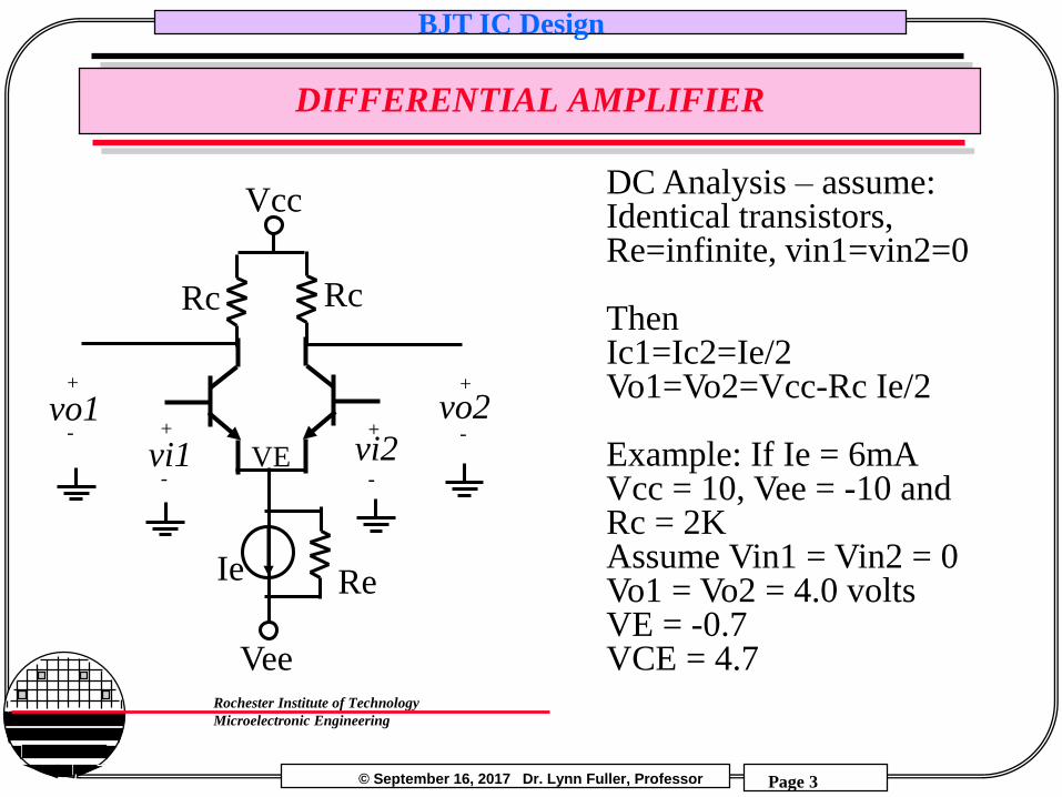
EXAMPLE FROM LAB
RC1
10 k
6 mA
–VEE = –12 V
vid
vo
Q2 Q1
100
VCC = +12 V
100
RC2
~
10 F
10 F RE2
RE1
RL
RC3
Q3
Q5
Q4 Q2N3904
Q2N3906
Q2N3906
100
100
Q6 Q2N3904
Q7 Q2N3906 See lab notes
© September 16, 2017 Dr. Lynn Fuller, Professor
Rochester Institute of Technology
Microelectronic Engineering
BJT IC Design
Page 40
REFERENCES
1. Sedra and Smith,
2. Device Electronics for Integrated Circuits, 2nd Edition, Kamins
and Muller, John Wiley and Sons, 1986.
3. The Bipolar Junction Transistor, 2nd Edition, Gerald Neudeck,
Addison-Wesley, 1989.
4. Analog Integrated Circuits, Gray and Meyers

© September 16, 2017 Dr. Lynn Fuller, Professor
Rochester Institute of Technology
Microelectronic Engineering
BJT IC Design
Page 41
HOMEWORK – BIPOLAR IC DESIGN
1. Derive the exact value of Ree for the current source on page 16.
2. Design a 100 µA current source.
3. For the simple op amp shown on page 31
a. let vin1 = vin2 = zero. Select values for Rc and Rb such
that Vout = zero.
b. What is the maximum load current before current
limiting?
c. Calculate the small signal differential voltage gain.
4. Do a SPICE analysis of the simple op amp on page 31. Show
DC Vout vs Vin and Voltage Gain. Answer: Gain ~128
5. Do a SPICE analysis of the differential amplifier using active
loads shown on page 33. Let V=10volts. Show DC Vout vs
Vin and Gain. Answer: Answer: Gain ~2000

© September 16, 2017 Dr. Lynn Fuller, Professor
Rochester Institute of Technology
Microelectronic Engineering
BJT IC Design
Page 42
CURRENT SOURCE (HW Problem 1)
There are many types of current sources. Consider the following:
4.3K
-10
T15K
ReeIe
What is Ie? (Ans: 1mA)
5K
b ib
rpvbe+
-vtest
+
-
5K
4.3K
ib
5K
itest
ro
Ree = infinity if ro = infinite (not there)
Ree is calculated by students in pro.1.
Ree in this example is 4.68 Meg
if b = 100 and ro = 100K
rp = b(0.026/1mA)
= 100 (26)= 2.6K

© September 16, 2017 Dr. Lynn Fuller, Professor
Rochester Institute of Technology
Microelectronic Engineering
BJT IC Design
Page 43
SOLUTION TO EXAMPLE ON PAGE 9
Analyze the following differential amplifier, b=200
2K
vi1
2K
vi2
vo2
+
-
+
-
-10
+10
T1 T21K1K

© September 16, 2017 Dr. Lynn Fuller, Professor
Rochester Institute of Technology
Microelectronic Engineering
BJT IC Design
Page 44
SOLUTION TO EXAMPLE ON PAGE 9
DC analysis: if Vin1 = Vin2 = zero, IC1 = IC2 and IB1=IB2
KVL: IB 1K + 0.7 + 2(b+1)IB 2K –10 = 0
IB = 9.3 / (1K+2(200+1) 2K = 11.6uA
IC = 200 IB = 2.32 mA
VCE1 =10 – - IB 1K - - 0.7 = 10.7
VCE2 = 10- IC 2K – - 0.7 = 6.06
rp = bVT / IC = 200 (0.026V)/2.32 mA = 2.24K
© September 16, 2017 Dr. Lynn Fuller, Professor
Rochester Institute of Technology
Microelectronic Engineering
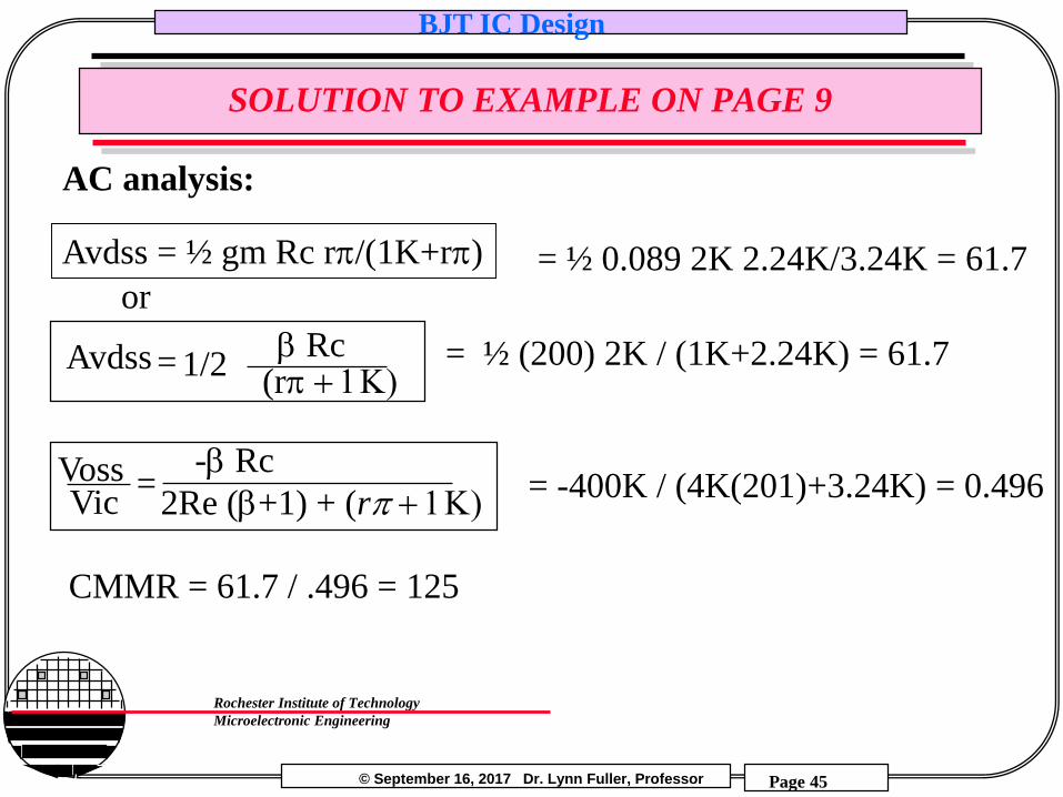
BJT IC Design
Page 45
SOLUTION TO EXAMPLE ON PAGE 9
Avdss =b Rc
(rp 1K)1/2
-b Rc
2Re (b+1) + (rp 1K)Voss Vic
=
AC analysis:
= ½ (200) 2K / (1K+2.24K) = 61.7
= -400K / (4K(201)+3.24K) = 0.496
CMMR = 61.7 / .496 = 125
Avdss = ½ gm Rc rp/(1K+rp) = ½ 0.089 2K 2.24K/3.24K = 61.7or

Do the DC analysis of this circuit.
Find the small signal voltage gain Vout/Vin,
Input resistance and output resistance.
Beta = 100
VA = infinite
+9
Vin2.2K
Vout20uA+-
Class Examples

Beta=100, VA = very large.
1.1 Do the DC analysis of this circuit with Vs=zero. What is Vout (offset voltage)?
1.2. Calculate the voltage gain, Avmid.
1.3 What could be done to reduce the offset voltage and increase the gain at the same time?
4K
VCC =10
1.2K
1K
1K
1.2K
Vs +- Vout
2K
VEE =-10
Vin+
-
1KQ1
Q4
Q2
Q3
Q5
Class Examples