Embed Size (px)
Citation preview
ESE319 Introduction to Microelectronics
12008 by Kenneth R. Laker (based on P.V. Lopresti 2006) update 09Sep08 KRL)
BJT Intro and Large Signal Model

ESE319 Introduction to Microelectronics
22008 by Kenneth R. Laker (based on P.V. Lopresti 2006) update 09Sep08 KRL)
Why BJT?What's the competition to BJT and bipolar technologies?
What advantages does the competition have over BJT?
What advantages does BJT and bipolar have over their com-petition?
What circuit applications benefit from BJT and bipolar tech-nologies?

ESE319 Introduction to Microelectronics
32008 by Kenneth R. Laker (based on P.V. Lopresti 2006) update 09Sep08 KRL)
Why BJTWhat's the competition to BJT and bipolar technologies?
MOSFET, in particular CMOS is the leading competitor
What advantages does the competition have over BJT?Small size (die area), low cost and low power dissipation
What advantages does BJT and bipolar have over their competi-tion?
High frequency operation, high current drive, high reliability in severe environmental conditions.
What circuit applications benefit from BJT and bipolar technolo-gies?
RF analog and digital circuits,power electronics and power am-plifiers, automobile electronics, radiation hardened electronics
ESE319 Introduction to Microelectronics
42008 by Kenneth R. Laker (based on P.V. Lopresti 2006) update 09Sep08 KRL)
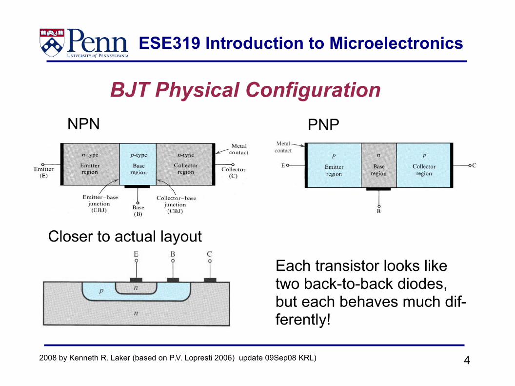
BJT Physical Configuration
Each transistor looks like two back-to-back diodes, but each behaves much dif-ferently!
NPN PNP
Closer to actual layout
ESE319 Introduction to Microelectronics
52008 by Kenneth R. Laker (based on P.V. Lopresti 2006) update 09Sep08 KRL)
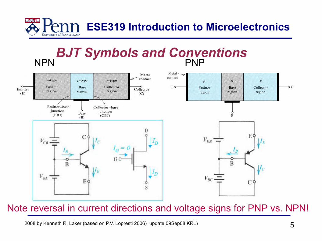
BJT Symbols and ConventionsNPN PNP
Note reversal in current directions and voltage signs for PNP vs. NPN!
ESE319 Introduction to Microelectronics
62008 by Kenneth R. Laker (based on P.V. Lopresti 2006) update 09Sep08 KRL)
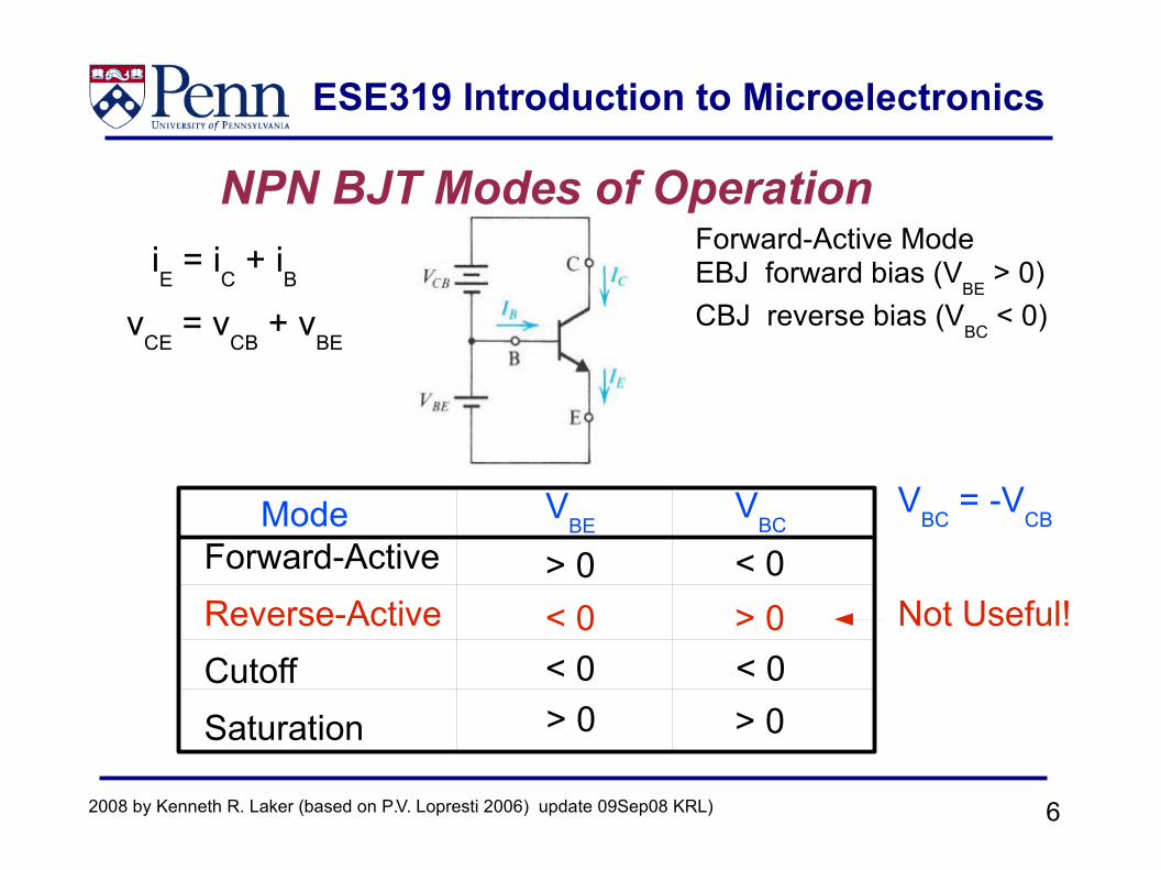
NPN BJT Modes of Operation
ModeForward-ActiveReverse-ActiveCutoffSaturation
VBE
VBC
> 0 < 0< 0 > 0< 0 < 0> 0 > 0
Forward-Active ModeEBJ forward bias (V
BE > 0)
CBJ reverse bias (VBC
< 0)
Not Useful!
VBC
= -VCB
vCE
= vCB
+ vBE
iE = i
C + i
B
ESE319 Introduction to Microelectronics
72008 by Kenneth R. Laker (based on P.V. Lopresti 2006) update 09Sep08 KRL)
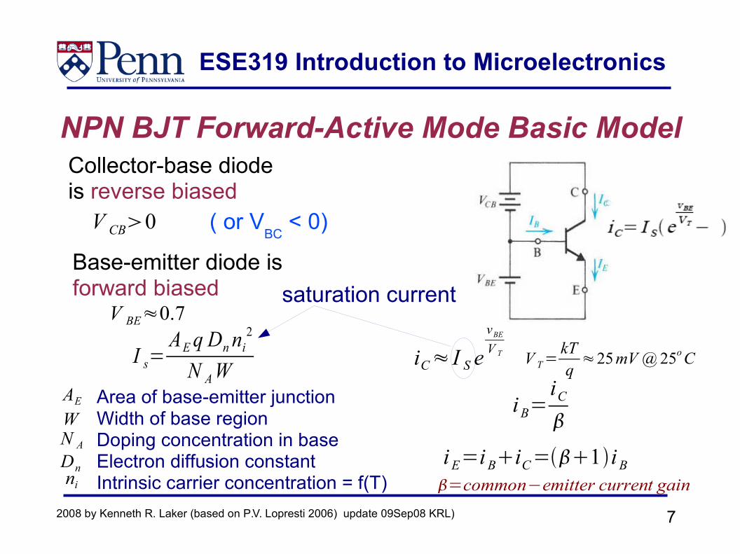
NPN BJT Forward-Active Mode Basic ModelCollector-base diode is reverse biasedV CB0
Base-emitter diode is forward biased
V BE≈0.7
iC≈ I S evBEV T
iB=iC
iE=iBiC=1iB
V T=kTq≈25mV @ 25oCI s=
AEq Dnni2
N AWArea of base-emitter junctionWidth of base regionDoping concentration in baseElectron diffusion constant Intrinsic carrier concentration = f(T) =common−emitter current gain
( or VBC
< 0)
saturation current
AEWN A
niDn
ESE319 Introduction to Microelectronics
82008 by Kenneth R. Laker (based on P.V. Lopresti 2006) update 09Sep08 KRL)
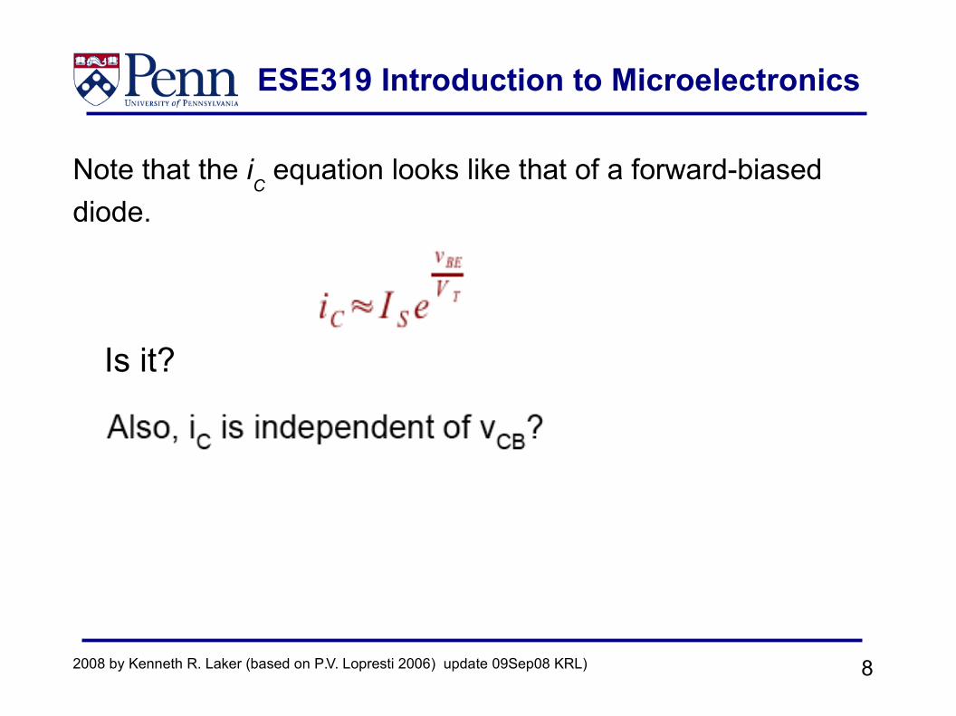
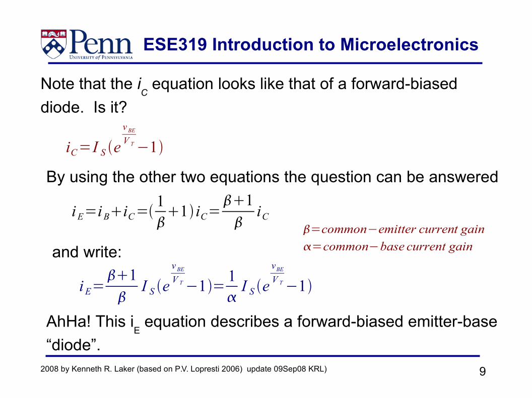
Note that the iC equation looks like that of a forward-biased
diode.
Is it?
ESE319 Introduction to Microelectronics
92008 by Kenneth R. Laker (based on P.V. Lopresti 2006) update 09Sep08 KRL)
Note that the iC equation looks like that of a forward-biased
diode. Is it?
iC=I S ev BEV T−1
By using the other two equations the question can be answered
iE=iBiC=11 iC=
1iC
and write:
iE=1I S e
v BEV T−1= 1
I S e
vBEV T−1
AhHa! This iE equation describes a forward-biased emitter-base
“diode”.
=common−emitter current gain=common−base current gain
ESE319 Introduction to Microelectronics
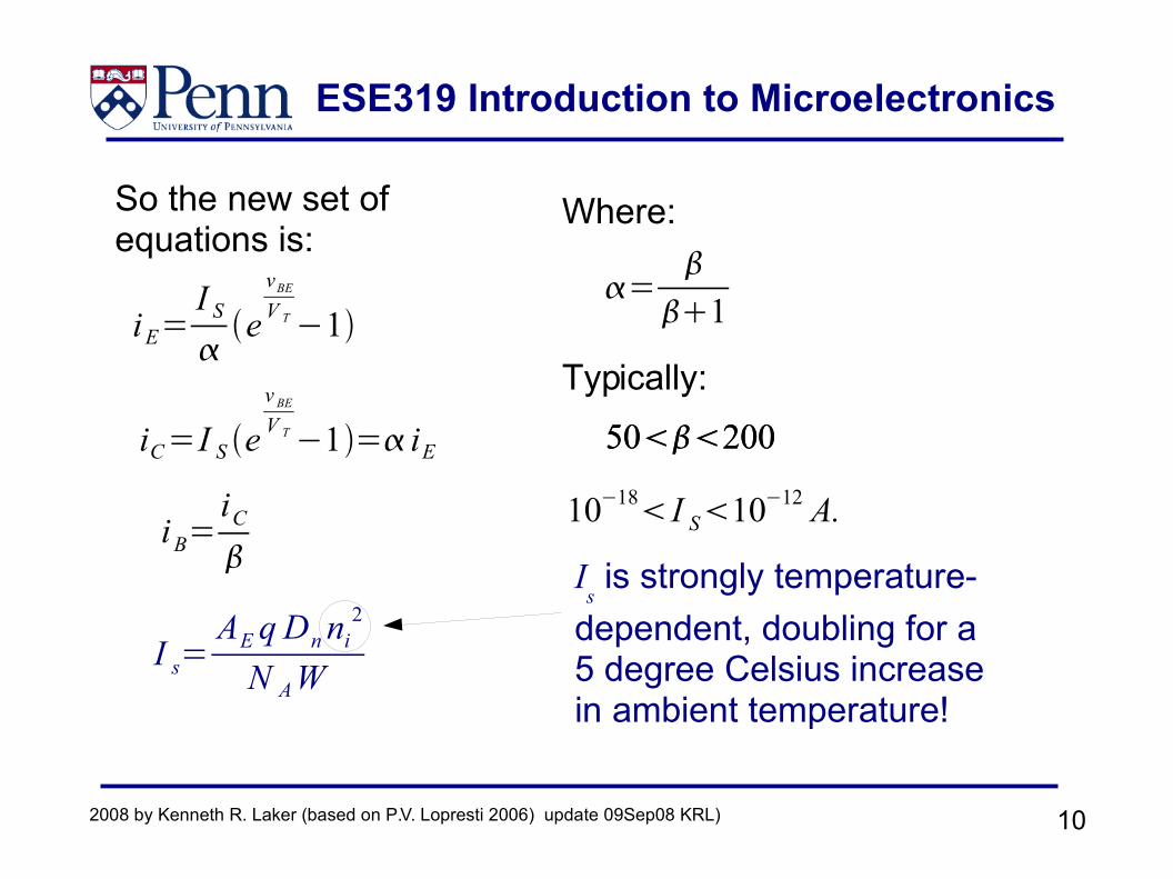
102008 by Kenneth R. Laker (based on P.V. Lopresti 2006) update 09Sep08 KRL)
So the new set ofequations is:
iC=I S ev BEV T−1= iE
iE=I Se
vBEV T−1
iB=iC
=
1
Where:
50200
10−18 I S10−12 A.
Typically:
Is is strongly temperature-
dependent, doubling for a 5 degree Celsius increase in ambient temperature!
50200
I s=AE q Dnni
2
N AW
ESE319 Introduction to Microelectronics
112008 by Kenneth R. Laker (based on P.V. Lopresti 2006) update 09Sep08 KRL)
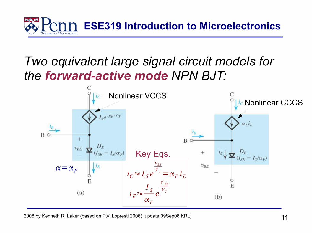
Two equivalent large signal circuit models for the forward-active mode NPN BJT:
Nonlinear VCCSNonlinear CCCS
iC≈ I S evBEV T=F iE
iE≈I SFeV BE
V T
Key Eqs.=F
ESE319 Introduction to Microelectronics
122008 by Kenneth R. Laker (based on P.V. Lopresti 2006) update 09Sep08 KRL)
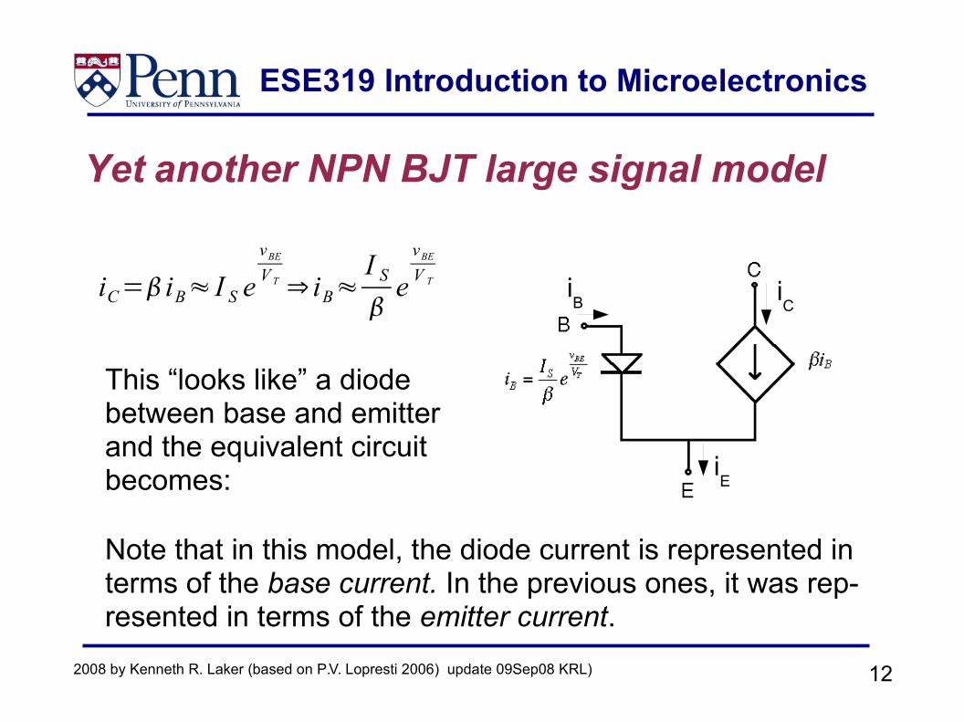
Yet another NPN BJT large signal model
iC= iB≈ I S evBEV T ⇒ iB≈
I SevBEV T
This “looks like” a diode between base and emitter and the equivalent circuit becomes:
Note that in this model, the diode current is represented in terms of the base current. In the previous ones, it was rep-resented in terms of the emitter current.
iB i
C
iE
ESE319 Introduction to Microelectronics
132008 by Kenneth R. Laker (based on P.V. Lopresti 2006) update 09Sep08 KRL)
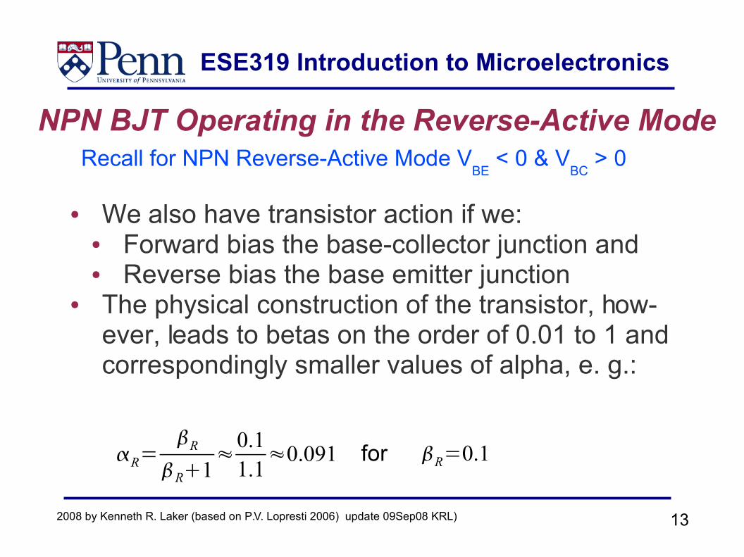
NPN BJT Operating in the Reverse-Active Mode
● We also have transistor action if we:● Forward bias the base-collector junction and● Reverse bias the base emitter junction
● The physical construction of the transistor, how-ever, leads to betas on the order of 0.01 to 1 and correspondingly smaller values of alpha, e. g.:
R=R
R1≈0.11.1
≈0.091 for R=0.1
Recall for NPN Reverse-Active Mode VBE
< 0 & VBC
> 0
ESE319 Introduction to Microelectronics
142008 by Kenneth R. Laker (based on P.V. Lopresti 2006) update 09Sep08 KRL)
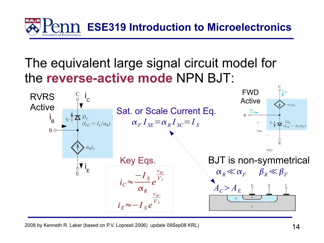
The equivalent large signal circuit model for the reverse-active mode NPN BJT:
iC≈−I SRevBCV T
iE≈−I S evBCV T
iB
iC
iE
RVRS Active
FWD Active
Key Eqs.
F I SE=R I SC=I SSat. or Scale Current Eq.
ACAE
BJT is non-symmetricalR≪F R≪F
ESE319 Introduction to Microelectronics
152008 by Kenneth R. Laker (based on P.V. Lopresti 2006) update 09Sep08 KRL)
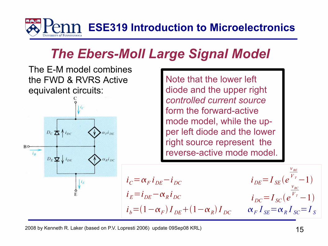
The Ebers-Moll Large Signal ModelThe E-M model combines the FWD & RVRS Active equivalent circuits:
Note that the lower left diode and the upper right controlled current source form the forward-active mode model, while the up-per left diode and the lower right source represent the reverse-active mode model.
iC=F iDE−iDCiE=iDE−R iDCib=1−F I DE1−R I DC
iDE=I SE ev BEV T−1
iDC=I SC evBCV T −1
F I SE=R I SC=I S
ESE319 Introduction to Microelectronics
162008 by Kenneth R. Laker (based on P.V. Lopresti 2006) update 09Sep08 KRL)
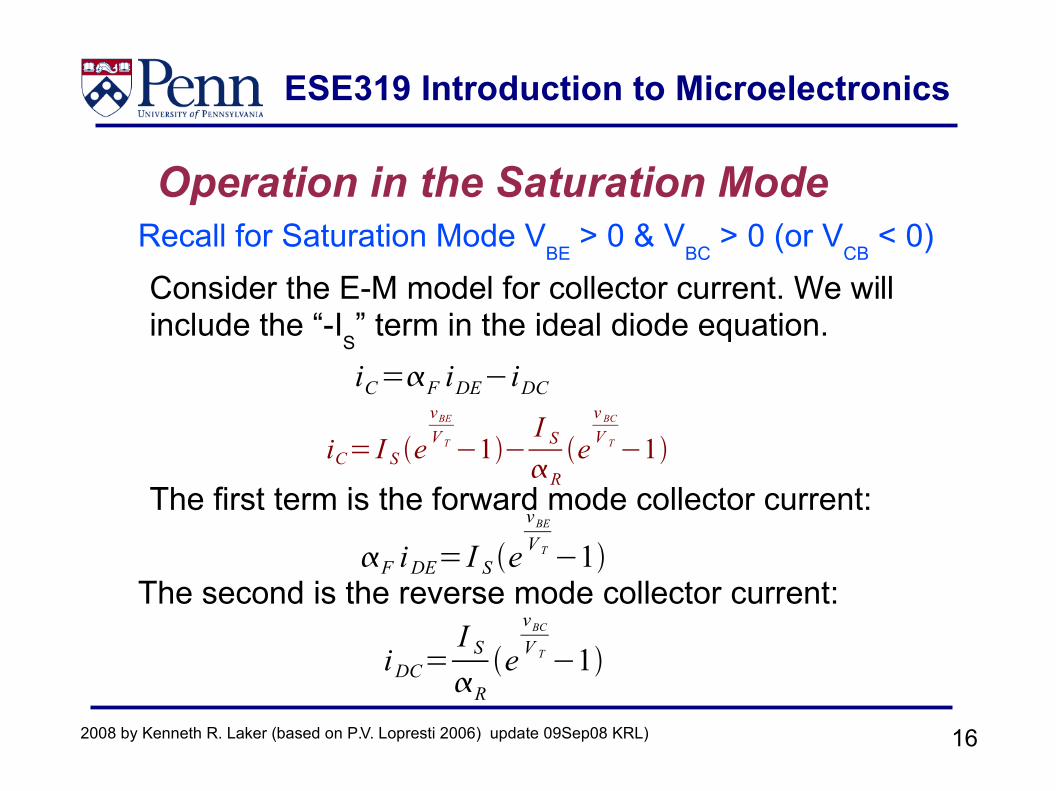
Operation in the Saturation Mode
Consider the E-M model for collector current. We will include the “-I
S” term in the ideal diode equation.iC=F iDE−iDC
The first term is the forward mode collector current:
F iDE= I S evBEV T −1
The second is the reverse mode collector current:
iDC=I SR
evBCV T −1
Recall for Saturation Mode VBE
> 0 & VBC
> 0 (or VCB
< 0)
iC= I S evBEV T−1−
I SR
ev BCV T−1
ESE319 Introduction to Microelectronics
172008 by Kenneth R. Laker (based on P.V. Lopresti 2006) update 09Sep08 KRL)
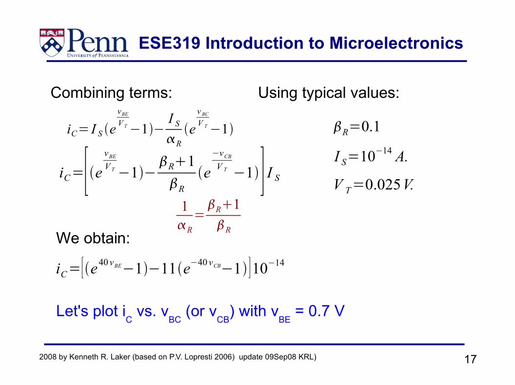
Combining terms:
iC=[e vBEV T −1− R1R
e−vCBV T −1] I S
Using typical values:
R=0.1
I S=10−14 A.
V T=0.025V.
iC=[e40 vBE−1−11e−40 vCB−1 ]10−14We obtain:
1R
=R1R
iC= I S evBEV T−1−
I SR
ev BCV T−1
Let's plot iC vs. v
BC (or v
CB) with v
BE = 0.7 V
ESE319 Introduction to Microelectronics
182008 by Kenneth R. Laker (based on P.V. Lopresti 2006) update 09Sep08 KRL)
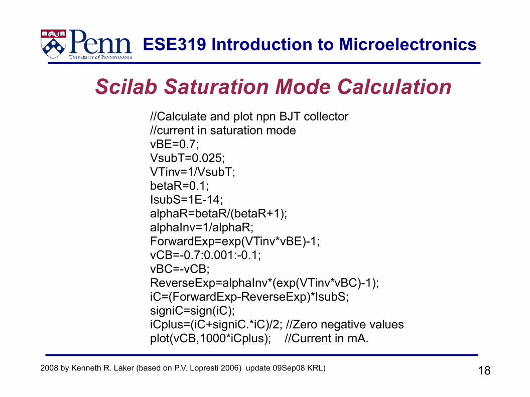
Scilab Saturation Mode Calculation//Calculate and plot npn BJT collector//current in saturation modevBE=0.7;VsubT=0.025;VTinv=1/VsubT;betaR=0.1;IsubS=1E-14;alphaR=betaR/(betaR+1);alphaInv=1/alphaR;ForwardExp=exp(VTinv*vBE)-1;vCB=-0.7:0.001:-0.1;vBC=-vCB;ReverseExp=alphaInv*(exp(VTinv*vBC)-1);iC=(ForwardExp-ReverseExp)*IsubS;signiC=sign(iC);iCplus=(iC+signiC.*iC)/2; //Zero negative valuesplot(vCB,1000*iCplus); //Current in mA.
ESE319 Introduction to Microelectronics
192008 by Kenneth R. Laker (based on P.V. Lopresti 2006) update 09Sep08 KRL)
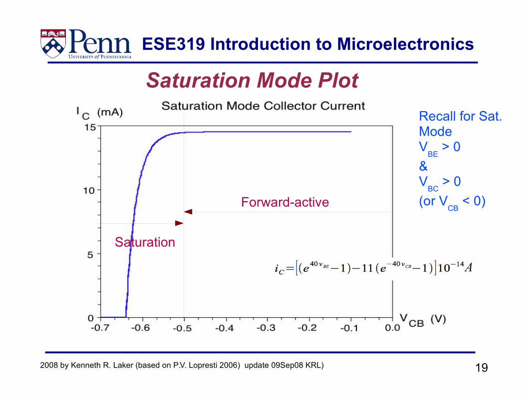
Saturation Mode Plot
Forward-active
Saturation
Recall for Sat. Mode V
BE > 0
& V
BC > 0
(or VCB
< 0)
A
ESE319 Introduction to Microelectronics
202008 by Kenneth R. Laker (based on P.V. Lopresti 2006) update 09Sep08 KRL)
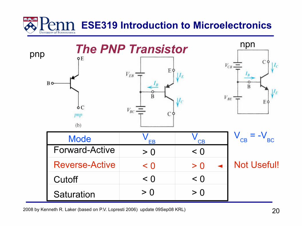
The PNP Transistor npnpnp
ModeForward-ActiveReverse-ActiveCutoffSaturation
VEB
VCB
> 0 < 0< 0 > 0< 0 < 0
> 0
Not Useful!
VCB
= -VBC
> 0
ESE319 Introduction to Microelectronics
212008 by Kenneth R. Laker (based on P.V. Lopresti 2006) update 09Sep08 KRL)
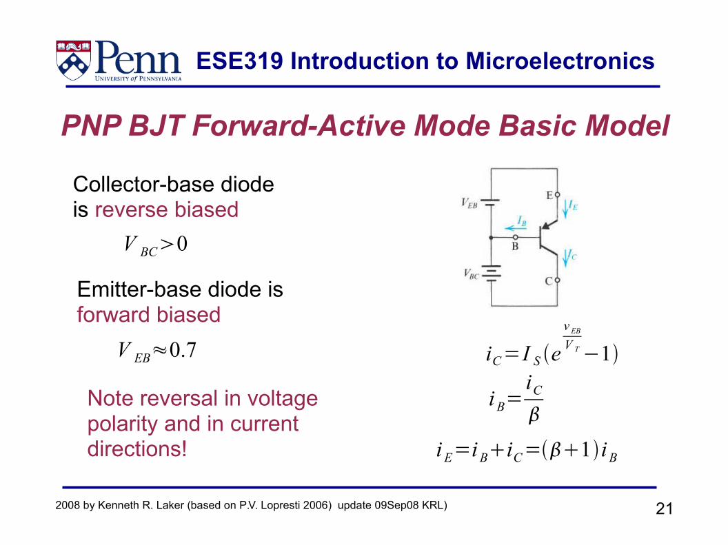
PNP BJT Forward-Active Mode Basic Model
Collector-base diode is reverse biased
V BC0
Emitter-base diode is forward biased
V EB≈0.7 iC=I S ev EBV T−1
iB=iC
iE=iBiC=1iB
Note reversal in voltage polarity and in current directions!
ESE319 Introduction to Microelectronics
222008 by Kenneth R. Laker (based on P.V. Lopresti 2006) update 09Sep08 KRL)
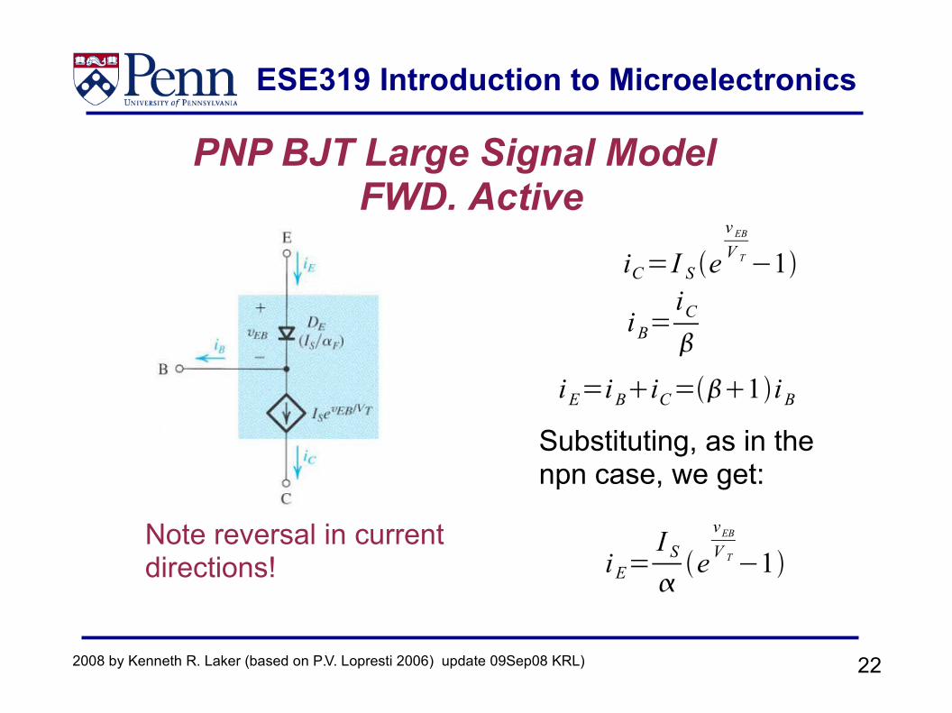
PNP BJT Large Signal Model FWD. Active
Note reversal in current directions!
iC=I S ev EBV T−1
iB=iC
iE=iBiC=1iBSubstituting, as in the npn case, we get:
iE=I Se
vEBV T−1
ESE319 Introduction to Microelectronics
232008 by Kenneth R. Laker (based on P.V. Lopresti 2006) update 09Sep08 KRL)
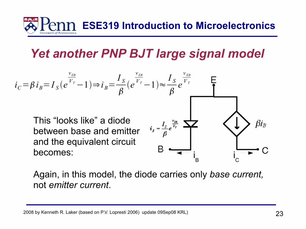
Yet another PNP BJT large signal model
This “looks like” a diode between base and emitter and the equivalent circuit becomes:
Again, in this model, the diode carries only base current, not emitter current.
iB
iC
iC= iB= I S evEBV T−1⇒ iB=
I Se
vEBV T−1≈
I Sev EBV T
ESE319 Introduction to Microelectronics
242008 by Kenneth R. Laker (based on P.V. Lopresti 2006) update 09Sep08 KRL)
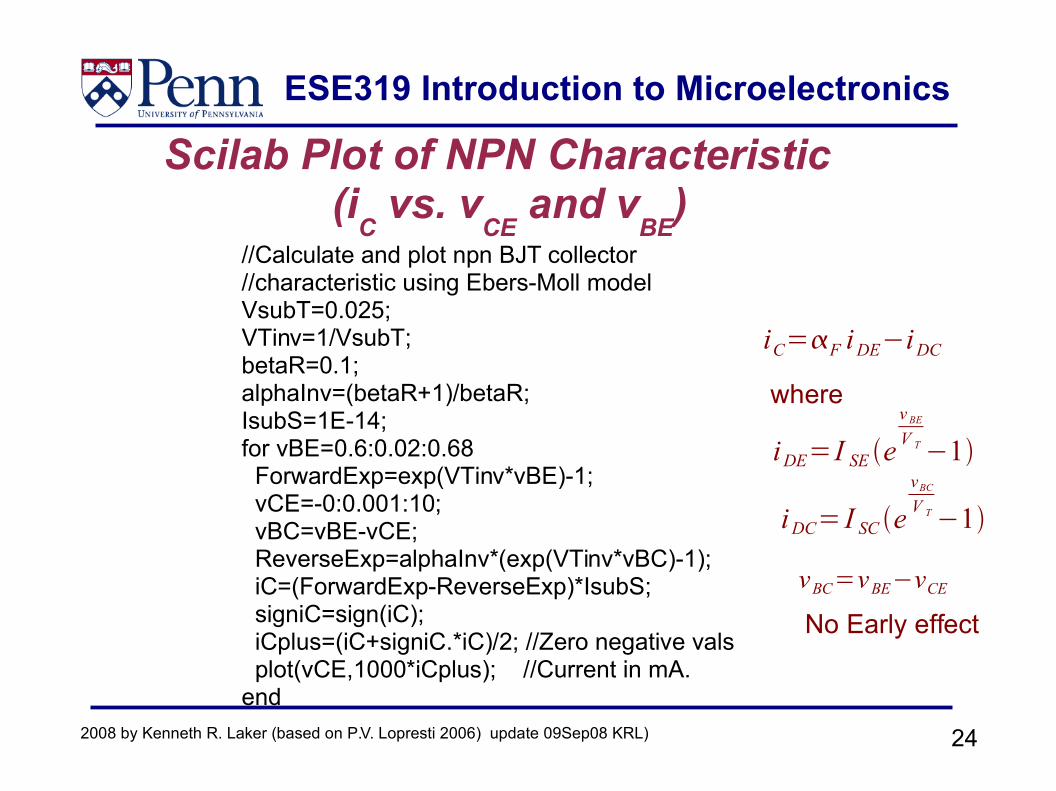
Scilab Plot of NPN Characteristic (i
C vs. v
CE and v
BE)
//Calculate and plot npn BJT collector//characteristic using Ebers-Moll modelVsubT=0.025;VTinv=1/VsubT;betaR=0.1;alphaInv=(betaR+1)/betaR;IsubS=1E-14;for vBE=0.6:0.02:0.68 ForwardExp=exp(VTinv*vBE)-1; vCE=-0:0.001:10; vBC=vBE-vCE; ReverseExp=alphaInv*(exp(VTinv*vBC)-1); iC=(ForwardExp-ReverseExp)*IsubS; signiC=sign(iC); iCplus=(iC+signiC.*iC)/2; //Zero negative vals plot(vCE,1000*iCplus); //Current in mA.end
iC=F iDE−iDC
iDC= I SC evBCV T−1
where
iDE=I SE ev BEV T−1
vBC=vBE−vCENo Early effect
ESE319 Introduction to Microelectronics
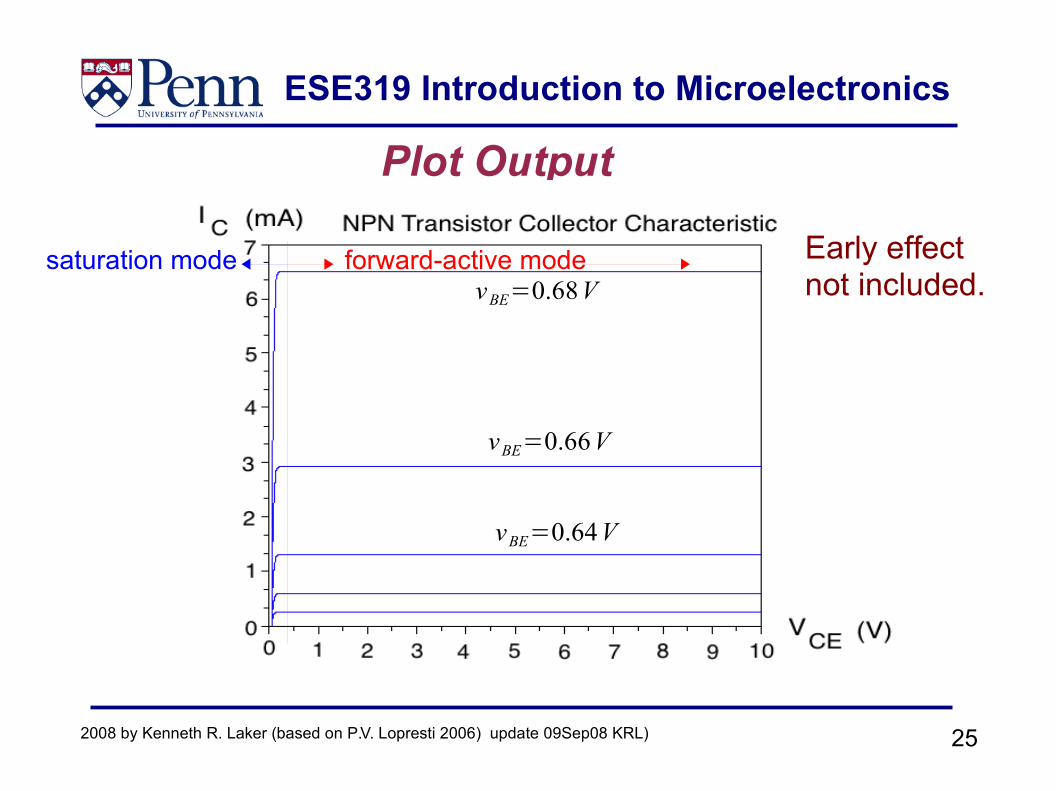
252008 by Kenneth R. Laker (based on P.V. Lopresti 2006) update 09Sep08 KRL)
Plot Output
vBE=0.68V
vBE=0.66V
vBE=0.64V
Early effect not included.
forward-active modesaturation mode
ESE319 Introduction to Microelectronics
262008 by Kenneth R. Laker (based on P.V. Lopresti 2006) update 09Sep08 KRL)
More on NPN Saturation● The base-collector diode has much larger
area than the base-emitter one.● Therefore, with the same applied voltage, it will
conduct a much larger forward current than will the base-emitter diode.
● When the collector-emitter voltage drops below the base-emitter voltage, the base-collector diode is forward biased and conducts heavily.
vCE≈V CE sat vCB=vCE−vBE when
ESE319 Introduction to Microelectronics
272008 by Kenneth R. Laker (based on P.V. Lopresti 2006) update 09Sep08 KRL)
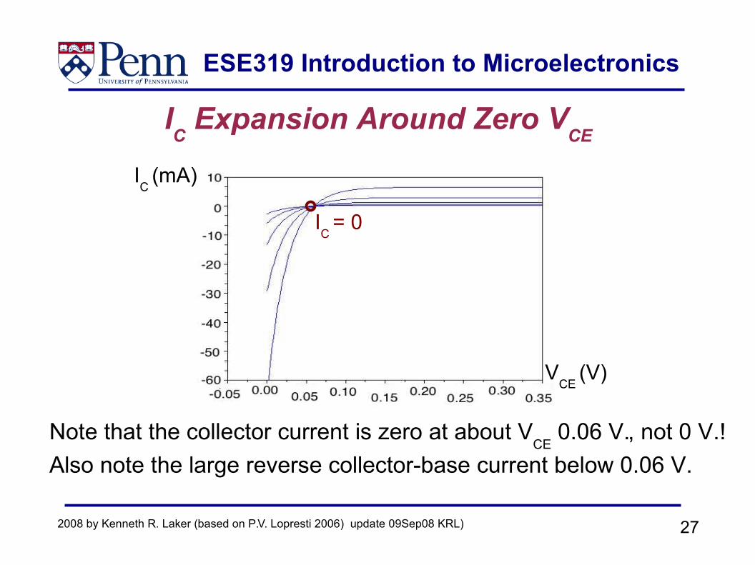
IC Expansion Around Zero V
CE
Note that the collector current is zero at about VCE
0.06 V., not 0 V.! Also note the large reverse collector-base current below 0.06 V.
IC
(mA)
VCE
(V)
IC
= 0
ESE319 Introduction to Microelectronics
282008 by Kenneth R. Laker (based on P.V. Lopresti 2006) update 09Sep08 KRL)
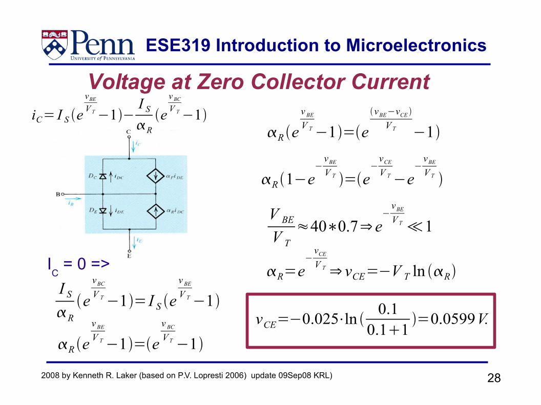
Voltage at Zero Collector Current
IC = 0 =>I SR
evBCV T−1= I S e
v BEV T−1
R ev BEV T−1=e
v BCV T −1
R ev BEV T−1=e
vBE−vCE V T −1
R 1−e−vBEV T =e
−vCEV T−e
−vBEV T
V BE
V T≈40∗0.7⇒ e
−vBEV T ≪1
R=e−vCEV T ⇒ vCE=−V T ln R
vCE=−0.025⋅ln 0.10.11
=0.0599V.
iC= I S evBEV T−1−
I SR
ev BCV T−1

![Lecture 4 BJT Small Signal Analysis01 [??????????????????]pws.npru.ac.th/thawatchait/data/files/Lecture 4 BJT Small... · 2016-09-12 · Lecture 4 BJJg yT Small Signal Analysis Present](https://img.pdfslide.net/doc/110x75/5e674360ee8da93175055e37/lecture-4-bjt-small-signal-analysis01-pwsnpruacththawatchaitdatafileslecture.jpg)