Embed Size (px)
Citation preview

a
Blackfin® FPGA EZ-Extender®
Manual
Revision 2.1, July 2012
Part Number82-000920-01
Analog Devices, Inc.One Technology WayNorwood, Mass. 02062-9106

Copyright Information© 2012 Analog Devices, Inc., ALL RIGHTS RESERVED. This docu-ment may not be reproduced in any form without prior, express written consent from Analog Devices, Inc.
Printed in the USA.
DisclaimerAnalog Devices, Inc. reserves the right to change this product without prior notice. Information furnished by Analog Devices is believed to be accurate and reliable. However, no responsibility is assumed by Analog Devices for its use; nor for any infringement of patents or other rights of third parties which may result from its use. No license is granted by impli-cation or otherwise under the patent rights of Analog Devices, Inc.
Trademark and Service Mark NoticeThe Analog Devices logo, Blackfin, CrossCore, EngineerZone, EZ-Extender, EZ-KIT Lite, and VisualDSP++ are registered trademarks of Analog Devices, Inc.
All other brand and product names are trademarks or service marks of their respective owners.

Regulatory Compliance The Blackfin FPGA EZ-Extender is designed to be used solely in a labora-tory environment. The board is not intended for use as a consumer end product or as a portion of a consumer end product. The board is an open system design which does not include a shielded enclosure and therefore may cause interference to other electrical devices in close proximity. This board should not be used in or near any medical equipment or RF devices.
The Blackfin FPGA EZ-Extender has been certified to comply with the essential requirements of the European EMC directive 89/336/EEC (inclusive 93/68/EEC) and, therefore, carries the “CE” mark.
The Blackfin FPGA EZ-Extender has been appended to Analog Devices Development Tools Technical Construction File referenced “DSPTOOLS1” dated December 21, 1997 and was awarded CE Certifi-cation by an appointed European Competent Body and is on file.
The Blackfin FPGA EZ-Extender contains ESD (electrostatic discharge) sensitive devices. Electrostatic charges readily accumulate on the human body and equipment and can discharge without detection. Permanent damage may occur on devices subjected to high-energy discharges. Proper ESD precautions are recommended to avoid performance degradation or loss of functionality. Store unused extender boards in the protective ship-ping package.

Blackfin FPGA EZ-Extender Manual v
CONTENTS
PREFACE
Product Overview .......................................................................... x
Purpose of This Manual ............................................................... xii
Intended Audience ....................................................................... xii
Manual Contents ......................................................................... xii
What’s New in This Manual ........................................................ xiii
Technical Support ....................................................................... xiii
Supported Products ...................................................................... xiv
Product Information ..................................................................... xv
Analog Devices Web Site ......................................................... xv
EngineerZone .......................................................................... xv
Related Documents ...................................................................... xvi
FPGA EZ-EXTENDER INTERFACES
FPGA EZ-Extender Setup ............................................................. 1-1
FPGA Software and Firmware ....................................................... 1-2
FPGA EZ-Extender Overview ....................................................... 1-3
Contents
vi Blackfin FPGA EZ-Extender Manual
FPGA EZ-EXTENDER HARDWARE REFERENCE
System Architecture ...................................................................... 2-2
Programming the FPGA ............................................................... 2-3
FPGA Programming via JTAG ................................................ 2-4
FPGA Programming via Serial ROM ....................................... 2-5
FPGA Programming via Blackfin Application .......................... 2-6
Programming the Serial ROM ....................................................... 2-7
Serial ROM via JTAG Header ................................................. 2-7
Power ........................................................................................... 2-8
Power In Header (P12) ............................................................ 2-9
3.3V Header (P13) .................................................................. 2-9
2.5V Header (P42) ................................................................ 2-10
1.2V Header (P43) ................................................................ 2-10
Jumpers ...................................................................................... 2-11
Serial ROM Boot Jumper (JP1) ............................................. 2-12
Config Done Jumper (JP2) .................................................... 2-12
Config Program Jumper (JP3) ............................................... 2-13
Boot Jumper (JP4) ................................................................ 2-13
FPGA Input Jumpers (JP5) ................................................... 2-14
Push Buttons and LEDs .............................................................. 2-15
Program Push Button (SW1) ................................................. 2-16
PB1 Push Button (SW3) ....................................................... 2-16
PB2 Push Button (SW4) ....................................................... 2-16
Status LEDs (LED1–8) ......................................................... 2-16
Blackfin FPGA EZ-Extender Manual vii
Contents
Power LED (LED9) ............................................................... 2-17
Done LED (LED10) ............................................................. 2-17
Connectors ................................................................................. 2-17
Expansion Interface (P1–3 and J1–3) ..................................... 2-18
IDC Connectors (P8, P14, P16, and P17) .............................. 2-19
IDC Connectors (P5 and P7) ................................................ 2-20
High-Speed Connector (P4) .................................................. 2-20
FPGA EZ-EXTENDER BILL OF MATERIALS
FPGA EZ-EXTENDER SCHEMATIC
INDEX

Contents
viii Blackfin FPGA EZ-Extender Manual

Blackfin FPGA EZ-Extender Manual ix
PREFACE
Thank you for purchasing the Blackfin® Field-Programmable Gate Array (FPGA) EZ-Extender®, Analog Devices, Inc. (ADI) extension board to the EZ-KIT Lite® evaluation system for ADSP-BF533, ADSP-BF537, and ADSP-BF561 Blackfin processors.
The Blackfin processors are embedded processors that support a Media Instruction Set Computing (MISC) architecture. This architecture is the natural merging of RISC, media functions, and digital signal processing characteristics towards delivering signal processing performance in a microprocessor-like environment.
The EZ-KIT Lite and FPGA EZ-Extender are designed to be used in con-junction with the CrossCore® Embedded Studio (CCES) and VisualDSP++® software development environments. The development environment facilitates advanced application code development and debug, such as:
• Create, compile, assemble, and link application programs written in C++, C, and FPGA EZ-Extender assembly
• Load, run, step, halt, and set breakpoints in application programs
• Read and write data and program memory
• Read and write core and peripheral registers
• Plot memory
To learn more about Analog Devices development software, go to http://www.analog.com/processors/tools.

Product Overview
x Blackfin FPGA EZ-Extender Manual
Product OverviewThe Blackfin FPGA EZ-Extender is a separately sold extension board that plugs onto the expansion interface of the ADSP-BF533, ADSP-BF537, or ADSP-BF561 EZ-KIT Lite evaluation system. The extension board aids the design and prototyping phases of ADSP-BF533, ADSP-BF537, or ADSP-BF561 processor targeted applications.
Please visit www.analog.com/EX1-FPGA for additional information, includ-ing CCES support.
The board extends the capabilities of the evaluation system by providing a Xilinx FPGA with external memory, IDC connectors for off-board con-nections, and a small bread board area.
The Blackfin FPGA EZ-Extender features:
• Xilinx Spartan III Field-Programmable Gate Array
• XC3S1000
• FG456 package
• Asynchronous static random access memory (SRAM)
• Directly connected to FPGA
• 2 MB (512K x 16 bits x 2 chips)
• TSOP44 package
Blackfin FPGA EZ-Extender Manual xi
Preface
• 25 MHz oscillator
• Directly connected to global clock of FPGA
• Socket for auxiliary oscillator
• Directly connected to global clock of FPGA
• IDC thru-hole connectors
• Allows quick access to Blackfin and FPGA pins for probing
• Allows access to Blackfin and FPGA pins for off-board connections
• High-speed connector
• Allows access to Blackfin and FPGA pins for high-speed application
• Expansion interface connectors
• Allows access to ADI’s family of Blackfin EZ-Extenders
• Two push buttons
• Directly connected to FPGA
• One with external debounce circuitry and one without
• Eight flag LEDs
• Directly connected to FPGA
Before using any of the interfaces, follow the setup procedure in “FPGA EZ-Extender Setup” on page 1-1.
Example programs are available to demonstrate the capabilities of the Blackfin FPGA EZ-Extender board.
Purpose of This Manual
xii Blackfin FPGA EZ-Extender Manual
Purpose of This ManualThe Blackfin FPGA EZ-Extender Manual describes the operation and con-figuration of the components on the extension board. A schematic and a bill of materials are provided as a reference for future Blackfin processor board designs.
Intended AudienceThis manual is a user’s guide and reference to the Blackfin FPGA EZ-Extender. Programmers who are familiar with the Analog Devices Blackfin processor architecture, operation, and development tools are the primary audience for this manual. The user should also be familiar with basic FPGA development and Xilinx’s Spartan III family of FPGAs.
Programmers who are unfamiliar with Analog Devices processors can use this manual but should supplement it with other texts that describe your target architecture. For the locations of these documents, see “Related Documents”.
Programmers who are unfamiliar with CCES or VisualDSP++ should refer to the online help and user’s manuals.
Manual ContentsThe manual consists of:
• Chapter 1, “FPGA EZ-Extender Interfaces” on page 1-1Provides basic board information.
• Chapter 2, “FPGA EZ-Extender Hardware Reference” on page 2-1Provides information on the hardware aspects of the board.
Blackfin FPGA EZ-Extender Manual xiii
Preface
• Appendix A, “FPGA EZ-Extender Bill of Materials” on page A-1Provides a list of components used to manufacture the EZ-Extender board.
• Appendix B, “FPGA EZ-Extender Schematic” on page B-1Provides the resources to allow EZ-KIT Lite board-level debugging or to use as a reference design. Appendix B is part of the online help.
What’s New in This ManualThis is revision 2.1 of the Blackfin FPGA EZ-Extender Manual. The man-ual has been updated to include CCES information. In addition, modifications and corrections based on errata reports against the previous manual revision have been made.
For the latest version of this manual, please refer to the Analog Devices Web site.
Technical SupportYou can reach Analog Devices processors and DSP technical support in the following ways:
• Post your questions in the processors and DSP support community at EngineerZone®:http://ez.analog.com/community/dsp
• Submit your questions to technical support directly at:http://www.analog.com/support

Supported Products
xiv Blackfin FPGA EZ-Extender Manual
• E-mail your questions about processors, DSPs, and tools develop-ment software from CrossCore Embedded Studio or VisualDSP++:
Choose Help > Email Support. This creates an e-mail [email protected] and automatically attaches your CrossCore Embedded Studio or VisualDSP++ version infor-mation and license.dat file.
• E-mail your questions about processors and processor applications to: [email protected] [email protected] (Greater China support)
• In the USA only, call 1-800-ANALOGD (1-800-262-5643)
• Contact your Analog Devices sales office or authorized distributor. Locate one at:www.analog.com/adi-sales
• Send questions by mail to:Processors and DSP Technical SupportAnalog Devices, Inc.Three Technology WayP.O. Box 9106Norwood, MA 02062-9106USA
Supported ProductsThe Blackfin FPGA EZ-Extender is designed as an extension board to the ADSP-BF533, ADSP-BF537, and ADSP-BF561 EZ-KIT Lite evaluation systems.
Blackfin FPGA EZ-Extender Manual xv
Preface
Product InformationProduct information can be obtained from the Analog Devices Web site and the online help.
Analog Devices Web SiteThe Analog Devices Web site, www.analog.com, provides information about a broad range of products—analog integrated circuits, amplifiers, converters, and digital signal processors.
To access a complete technical library for each processor family, go to http://www.analog.com/processors/technical_library. The manuals selection opens a list of current manuals related to the product as well as a link to the previous revisions of the manuals. When locating your manual title, note a possible errata check mark next to the title that leads to the current correction report against the manual.
Also note, MyAnalog is a free feature of the Analog Devices Web site that allows customization of a Web page to display only the latest information about products you are interested in. You can choose to receive weekly e-mail notifications containing updates to the Web pages that meet your interests, including documentation errata against all manuals. MyAnalog provides access to books, application notes, data sheets, code examples, and more.
Visit MyAnalog to sign up. If you are a registered user, just log on. Your user name is your e-mail address.
EngineerZoneEngineerZone is a technical support forum from Analog Devices. It allows you direct access to ADI technical support engineers. You can search FAQs and technical information to get quick answers to your embedded processing and DSP design questions.
Related Documents
xvi Blackfin FPGA EZ-Extender Manual
Use EngineerZone to connect with other DSP developers who face similar design challenges. You can also use this open forum to share knowledge and collaborate with the ADI support team and your peers. Visit http://ez.analog.com to sign up.
Related DocumentsFor additional information about the product, refer to the following publications.
For more information on the Xilinx Spartan III FPGA, refer to the data sheet located at www.xilinx.com.
Table 1. Related Processor Publications
Title Description
• ADSP-BF531/ADSP-BF532/ADSP-BF533 Blackfin Embedded Processor Data Sheet
• ADSP-BF534/ADSP-BF536/ADSP-BF537 Blackfin Embedded Processor Data Sheet
• ADSP-BF561 Blackfin Embedded Symmetric Multiprocessor Data Sheet
General functional description, pinout, and timing
• ADSP-BF533 Blackfin Processor Hardware Reference
• ADSP-BF537 Blackfin Processor Hardware Reference
• ADSP-BF561 Blackfin Processor Hardware Reference
Description of the internal processor architec-ture and all register functions
Blackfin Processor Programming Reference Description of all allowed processor assembly instructions
Blackfin FPGA EZ-Extender Manual 1-1
1 FPGA EZ-EXTENDER INTERFACES
This chapter provides the setup procedures for both the Blackfin Field-Programmable Gate Array (FPGA) EZ-Extender and EZ-KIT Lite (ADSP-BF533, ADSP-BF537 or ADSP-BF561). It also provides an over-view of the extender board.
The information is presented in the following order.
• “FPGA EZ-Extender Setup” on page 1-1
• “FPGA Software and Firmware” on page 1-2
• “FPGA EZ-Extender Overview” on page 1-3
FPGA EZ-Extender SetupIt is very important to set up all of the components of the system contain-ing the FPGA EZ-Extender before applying power to that system. The following procedure is recommended.
Power your system when these steps are completed:
1. Read the applicable design interface section in this chapter—the text provides an overview of the capabilities of the EZ-Extender.
2. Read “System Architecture” on page 2-2 to understand the physical connections of the extender board. For detailed information, refer to “FPGA EZ-Extender Schematic” on page B-1.

FPGA Software and Firmware
1-2 Blackfin FPGA EZ-Extender Manual
3. Remove any rubber feet attached to the EZ-KIT Lite if the feet cover the printed circuit board (PCB) mounting holes. In place of the rubber feet, install the four nylon feet and screws provided with the FPGA EZ-Extender. Install the nylon feet in the mounting holes of the EZ-KIT Lite’s PCB. Flip the EZ-KIT Lite upside down so that the three expansion headers (J1–3) are facing up.
4. Set the switches and jumpers on the FPGA EZ-Extender board. Use the block diagram in Figure 2-1 on page 2-2 in conjunction with “Jumpers” on page 2-11.
5. Set the switches and jumpers on the EZ-KIT Lite board. If not already, familiarize yourself with the documentation and schemat-ics of the EZ-KIT Lite (see “Related Documents”). Compare the expansion interface signals of the FPGA EZ-Extender board with the signals of the EZ-KIT Lite board to ensure there is no conten-tion. For example, it may be necessary to disable other devices connected to the expansion interface of the processor and disable the push buttons on the EZ-KIT Lite.
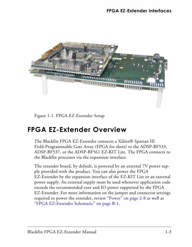
6. Install the FPGA EZ-Extender on the EZ-KIT Lite via the three-connector expansion interface. Figure 1-1 shows how an FPGA EZ-Extender plugs onto an EZ-KIT Lite.
7. Configure any other interfacing boards, for example, another EZ-Extender.
FPGA Software and FirmwareFor information on the FPGA software, refer to the readme text file located in the Examples folder of the installation directory.
Blackfin FPGA EZ-Extender Manual 1-3
FPGA EZ-Extender Interfaces
FPGA EZ-Extender OverviewThe Blackfin FPGA EZ-Extender connects a Xilinx® Spartan III Field-Programmable Gate Array (FPGA for short) to the ADSP-BF533, ADSP-BF537, or the ADSP-BF561 EZ-KIT Lite. The FPGA connects to the Blackfin processor via the expansion interface.
The extender board, by default, is powered by an external 7V power sup-ply provided with the product. You can also power the FPGA EZ-Extender by the expansion interface of the EZ-KIT Lite or an external power supply. An external supply must be used whenever application code exceeds the recommended core and IO power supported by the FPGA EZ-Extender. For more information on the jumper and connector settings required to power the extender, review “Power” on page 2-8 as well as “FPGA EZ-Extender Schematic” on page B-1.
Figure 1-1. FPGA EZ-Extender Setup

FPGA EZ-Extender Overview
1-4 Blackfin FPGA EZ-Extender Manual
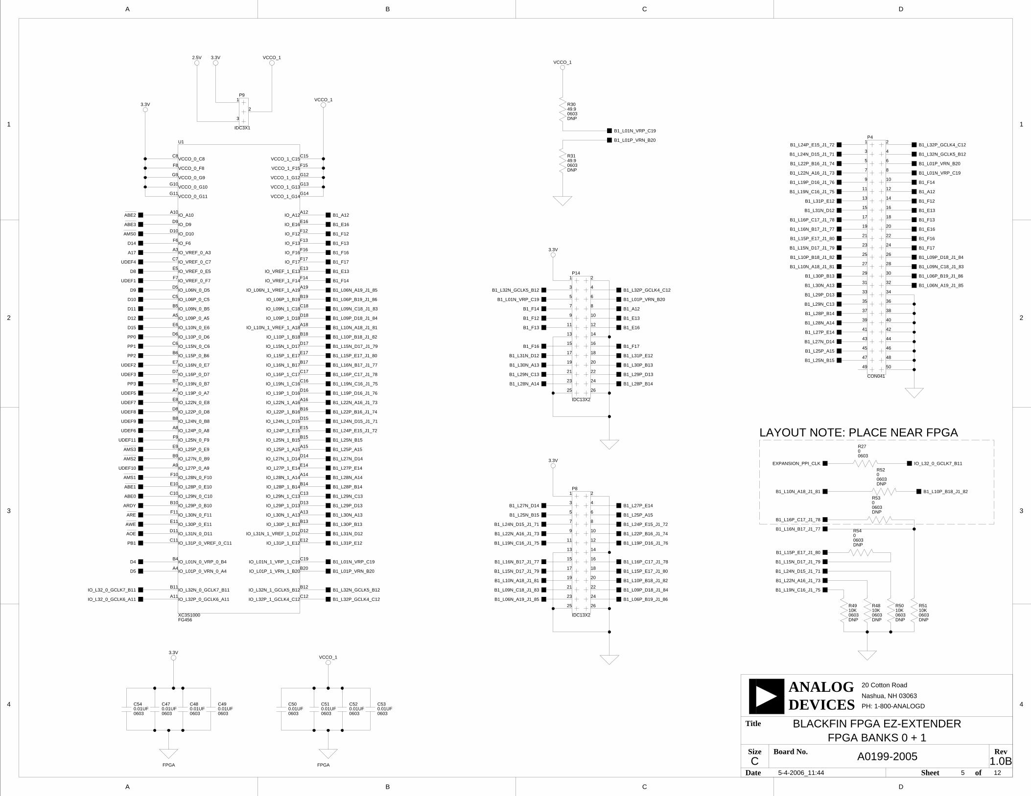
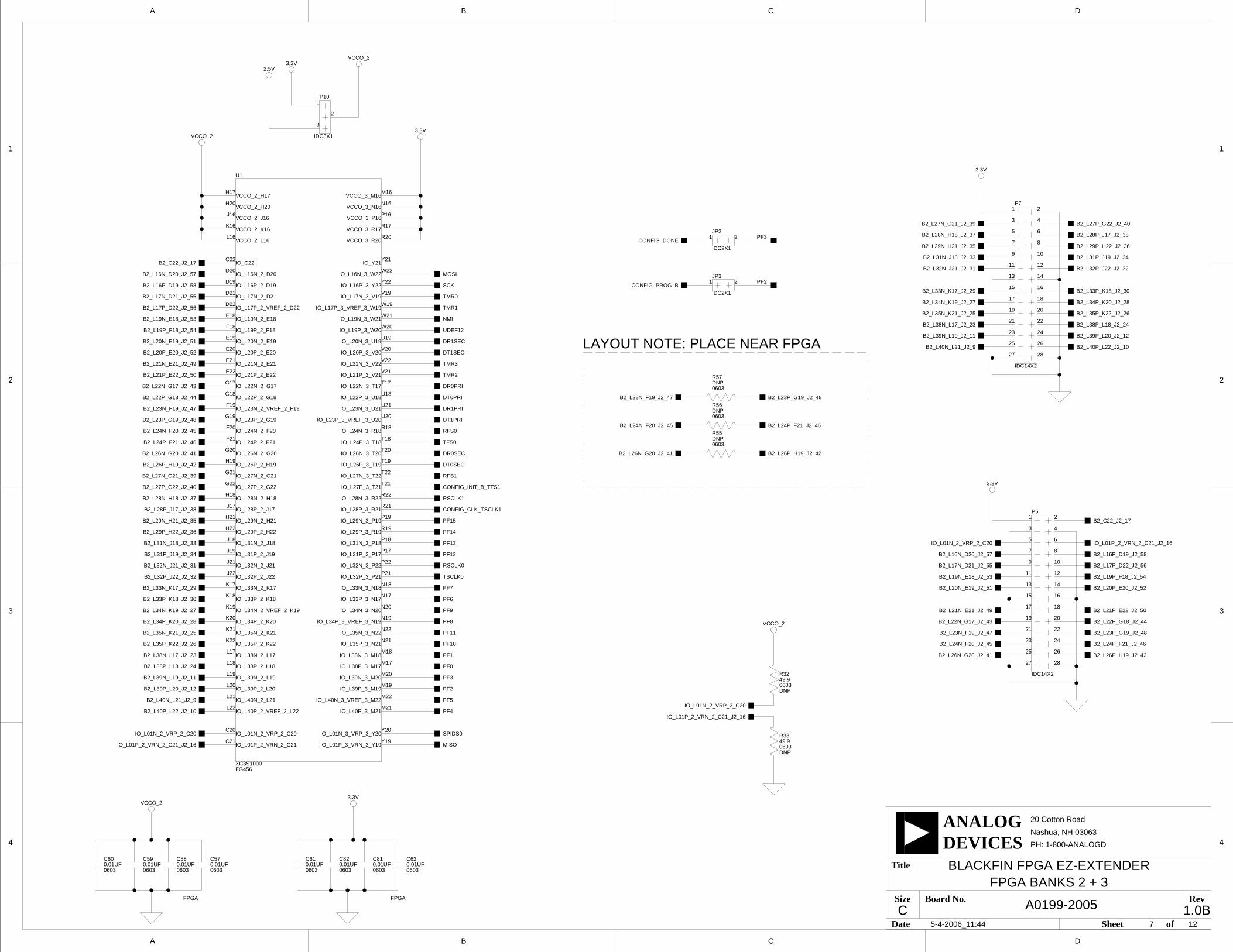
The FPGA EZ-Extender contains 2 MB of asynchronous SRAM memory, powered by a 3.3V supply. The SRAM memory connects to banks 6 and 7 of the FPGA and can perform simple data storage instructions in applica-tion-specific code.
The FPGA EZ-Extender includes a 25 MHz oscillator (U6) connected to the FPGA via the dedicated global clock 1 (GCLK1) pin, facilitating devel-opment of applications that require a clock. A second clock socket (U7) is left unpopulated to allow a user to place an oscillator with a specific fre-quency for the FPGA. The second clock socket connects to the global clock 6 (GCLK6) pin of the FPGA.
The extender has eight LEDs (LED1–8) and two push buttons (SW3–4) for applications that require status reporting and user control. The push but-tons are active low and when pressed, provide a logic 0 to the respective FPGA nets. For inputs that require a permanent input low, use the jumper inputs on JP4. When a jumper is populated on one of the four nets of JP4, the respective pin is hard wired to a logic 0. For more information about the LEDs, push button switches, and jumper inputs, refer to “FPGA EZ-Extender Hardware Reference” on page 2-1.
There are various ways to program the FPGA. By default, the FPGA is programmed in its slave serial mode by the flash programming utility in CCES or VisualDSP++. The program configures the FPGA using the Blackfin processor’s flag pins and/or serial port pins. For more informa-tion on how to use the flash programming utility within the development environment, refer to the readme file located in the Examples folder of the installation directory.
A second method of programming the FPGA is by using a Xilinx JTAG cable and software. The Xilinx JTAG cable connects to the FPGA JTAG header (P15). For more information about programming the FPGA via a Xilinx JTAG cable, refer to the manufacturer’s website at www.xilinx.com.
The third and final way to program the FPGA is via the Xilinx serial ROM on the FPGA EZ-Extender. The serial ROM used for FPGA is
Blackfin FPGA EZ-Extender Manual 1-5
FPGA EZ-Extender Interfaces
shipped with the extender and is pre-programmed. If the serial ROM needs to be re-programmed with new code, use an Xilinx JTAG cable and software and connect the Xilinx JTAG cable to the flash JTAG header (P6).
More information about programming the serial ROM can be found at www.xilinx.com. More details about the different ways to program the FPGA can be found in “FPGA EZ-Extender Hardware Reference” on page 2-1.
FPGA EZ-Extender Overview
1-6 Blackfin FPGA EZ-Extender Manual

Blackfin FPGA EZ-Extender Manual 2-1
2 FPGA EZ-EXTENDER HARDWARE REFERENCE
This chapter describes the hardware design of the Field-Programmable Gate Array (FPGA) EZ-Extender.
The following topics are covered.
• “System Architecture” on page 2-2Describes the configuration of the extender board and explains how the board components interface with the processor and EZ-KIT Lite.
• “Programming the FPGA” on page 2-3Describes the different methods of programming the FPGA.
• “Programming the Serial ROM” on page 2-7Describes the method of programming the serial ROM.
• “Power” on page 2-8Describes the methods to power the extender board.
• “Jumpers” on page 2-11Describes the function of the configuration jumpers.
• “Push Buttons and LEDs” on page 2-15Describes the function of the push buttons and LEDs.
• “Connectors” on page 2-17Describes the function of the extender connectors.
System Architecture
2-2 Blackfin FPGA EZ-Extender Manual
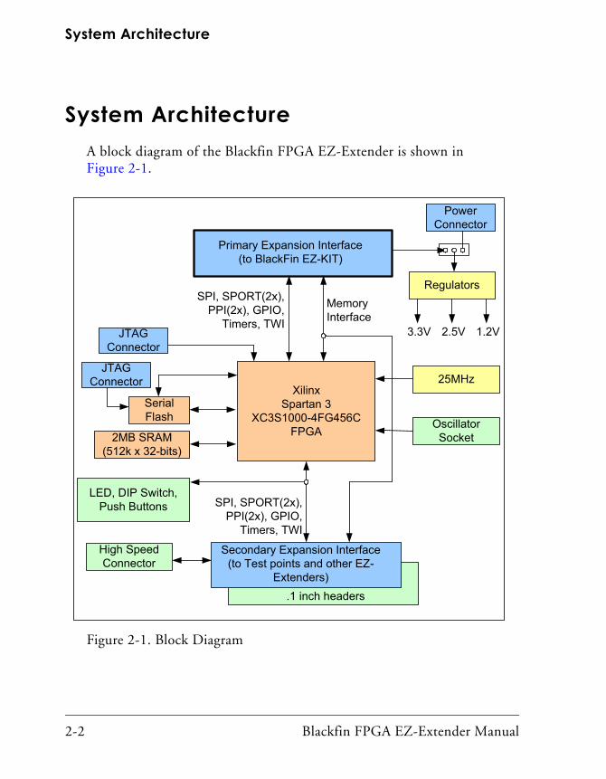
System ArchitectureA block diagram of the Blackfin FPGA EZ-Extender is shown in Figure 2-1.
Figure 2-1. Block Diagram
XilinxSpartan 3
XC3S1000-4FG456C FPGA2MB SRAM
(512k x 32-bits)
Memory Interface
SPI, SPORT(2x), PPI(2x), GPIO,
Timers, TWI
Primary Expansion Interface (to BlackFin EZ-KIT)
Secondary Expansion Interface (to Test points and other EZ-
Extenders)
Power Connector
Regulators
3.3V 2.5V 1.2V
.1 inch headers
25MHz
Oscillator Socket
LED, DIP Switch, Push Buttons
SPI, SPORT(2x), PPI(2x), GPIO,
Timers, TWI
Serial Flash
High Speed Connector
JTAG Connector
JTAG Connector
Blackfin FPGA EZ-Extender Manual 2-3
FPGA EZ-Extender Hardware Reference
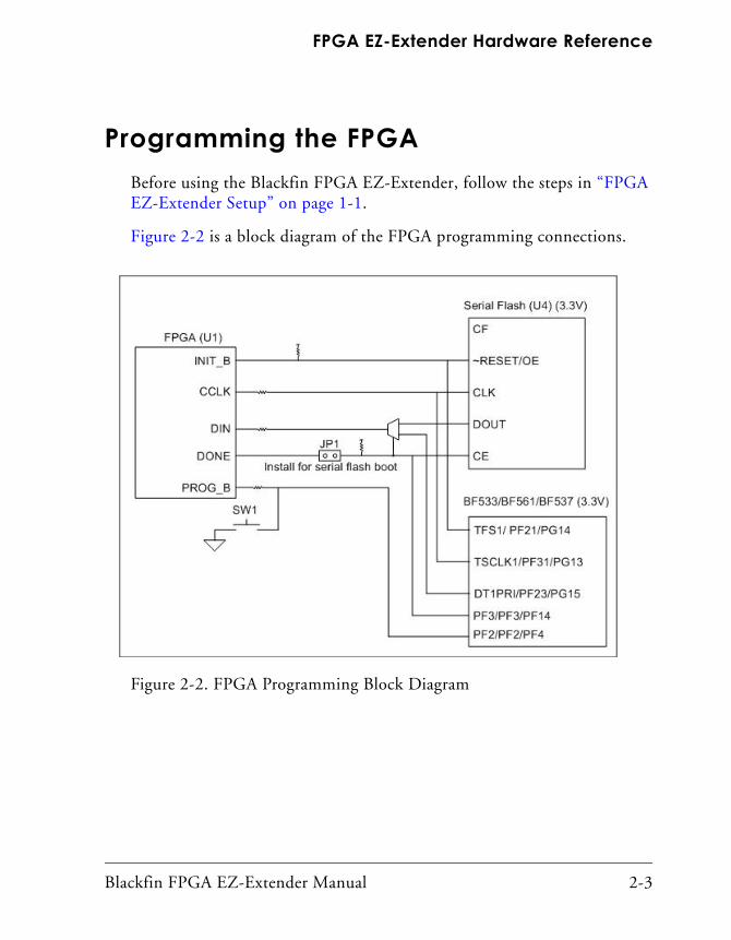
Programming the FPGABefore using the Blackfin FPGA EZ-Extender, follow the steps in “FPGA EZ-Extender Setup” on page 1-1.
Figure 2-2 is a block diagram of the FPGA programming connections.
Figure 2-2. FPGA Programming Block Diagram
Programming the FPGA
2-4 Blackfin FPGA EZ-Extender Manual
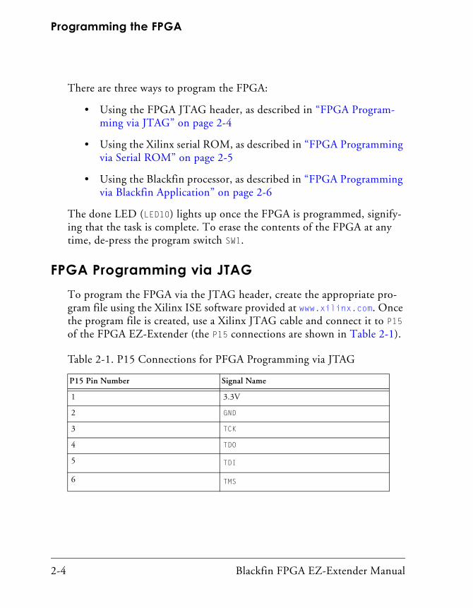
There are three ways to program the FPGA:
• Using the FPGA JTAG header, as described in “FPGA Program-ming via JTAG” on page 2-4
• Using the Xilinx serial ROM, as described in “FPGA Programming via Serial ROM” on page 2-5
• Using the Blackfin processor, as described in “FPGA Programming via Blackfin Application” on page 2-6
The done LED (LED10) lights up once the FPGA is programmed, signify-ing that the task is complete. To erase the contents of the FPGA at any time, de-press the program switch SW1.
FPGA Programming via JTAGTo program the FPGA via the JTAG header, create the appropriate pro-gram file using the Xilinx ISE software provided at www.xilinx.com. Once the program file is created, use a Xilinx JTAG cable and connect it to P15 of the FPGA EZ-Extender (the P15 connections are shown in Table 2-1).
Table 2-1. P15 Connections for PFGA Programming via JTAG
P15 Pin Number Signal Name
1 3.3V
2 GND
3 TCK
4 TDO
5 TDI
6 TMS
Blackfin FPGA EZ-Extender Manual 2-5
FPGA EZ-Extender Hardware Reference
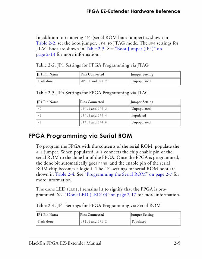
In addition to removing JP1 (serial ROM boot jumper) as shown in Table 2-2, set the boot jumper, JP4, to JTAG mode. The JP4 settings for JTAG boot are shown in Table 2-3. See “Boot Jumper (JP4)” on page 2-13 for more information.
FPGA Programming via Serial ROMTo program the FPGA with the contents of the serial ROM, populate the JP1 jumper. When populated, JP1 connects the chip enable pin of the serial ROM to the done bit of the FPGA. Once the FPGA is programmed, the done bit automatically goes high, and the enable pin of the serial ROM chip becomes a logic 1. The JP1 settings for serial ROM boot are shown in Table 2-4. See “Programming the Serial ROM” on page 2-7 for more information.
The done LED (LED10) remains lit to signify that the FPGA is pro-grammed. See “Done LED (LED10)” on page 2-17 for more information.
Table 2-2. JP1 Settings for FPGA Programming via JTAG
JP1 Pin Name Pins Connected Jumper Setting
Flash done JP1.1 and JP1.2 Unpopulated
Table 2-3. JP4 Settings for FPGA Programming via JTAG
JP4 Pin Name Pins Connected Jumper Setting
M0 JP4.1 and JP4.2 Unpopulated
M1 JP4.3 and JP4.4 Populated
M2 JP4.5 and JP4.6 Unpopulated
Table 2-4. JP1 Settings for FPGA Programming via Serial ROM
JP1 Pin Name Pins Connected Jumper Setting
Flash done JP1.1 and JP1.2 Populated
Programming the FPGA
2-6 Blackfin FPGA EZ-Extender Manual
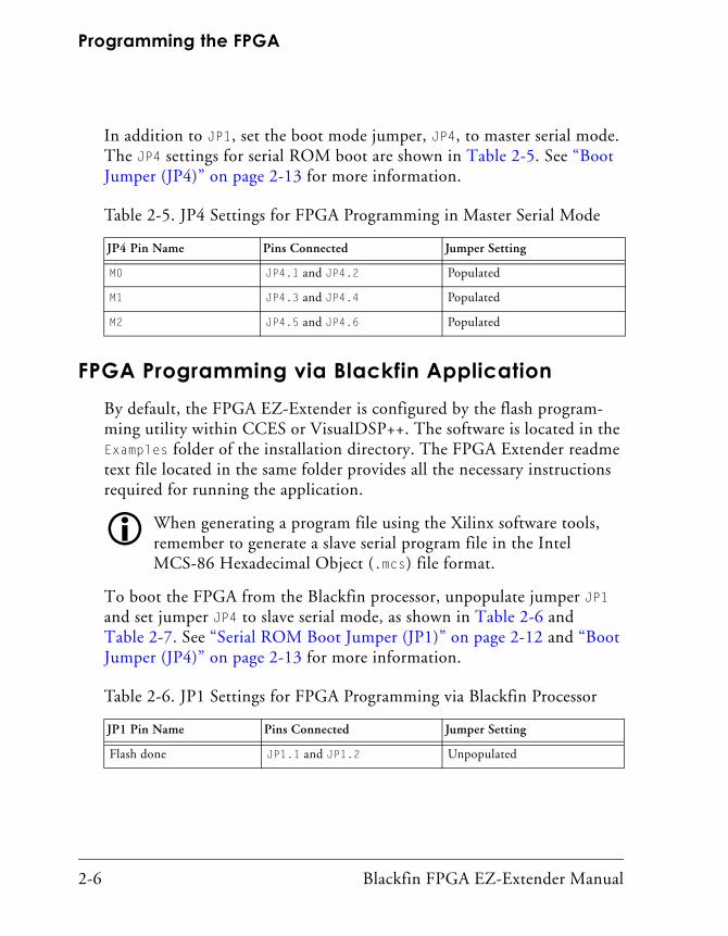
In addition to JP1, set the boot mode jumper, JP4, to master serial mode. The JP4 settings for serial ROM boot are shown in Table 2-5. See “Boot Jumper (JP4)” on page 2-13 for more information.
FPGA Programming via Blackfin ApplicationBy default, the FPGA EZ-Extender is configured by the flash program-ming utility within CCES or VisualDSP++. The software is located in the Examples folder of the installation directory. The FPGA Extender readme text file located in the same folder provides all the necessary instructions required for running the application.
When generating a program file using the Xilinx software tools, remember to generate a slave serial program file in the Intel MCS-86 Hexadecimal Object (.mcs) file format.
To boot the FPGA from the Blackfin processor, unpopulate jumper JP1 and set jumper JP4 to slave serial mode, as shown in Table 2-6 and Table 2-7. See “Serial ROM Boot Jumper (JP1)” on page 2-12 and “Boot Jumper (JP4)” on page 2-13 for more information.
Table 2-5. JP4 Settings for FPGA Programming in Master Serial Mode
JP4 Pin Name Pins Connected Jumper Setting
M0 JP4.1 and JP4.2 Populated
M1 JP4.3 and JP4.4 Populated
M2 JP4.5 and JP4.6 Populated
Table 2-6. JP1 Settings for FPGA Programming via Blackfin Processor
JP1 Pin Name Pins Connected Jumper Setting
Flash done JP1.1 and JP1.2 Unpopulated
Blackfin FPGA EZ-Extender Manual 2-7
FPGA EZ-Extender Hardware Reference
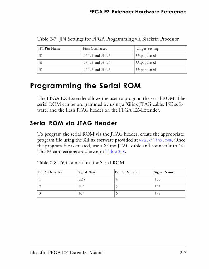
Programming the Serial ROMThe FPGA EZ-Extender allows the user to program the serial ROM. The serial ROM can be programmed by using a Xilinx JTAG cable, ISE soft-ware, and the flash JTAG header on the FPGA EZ-Extender.
Serial ROM via JTAG HeaderTo program the serial ROM via the JTAG header, create the appropriate program file using the Xilinx software provided at www.xilinx.com. Once the program file is created, use a Xilinx JTAG cable and connect it to P6. The P6 connections are shown in Table 2-8.
Table 2-7. JP4 Settings for FPGA Programming via Blackfin Processor
JP4 Pin Name Pins Connected Jumper Setting
M0 JP4.1 and JP4.2 Unpopulated
M1 JP4.3 and JP4.4 Unpopulated
M2 JP4.5 and JP4.6 Unpopulated
Table 2-8. P6 Connections for Serial ROM
P6 Pin Number Signal Name P6 Pin Number Signal Name
1 3.3V 4 TDO
2 GND 5 TDI
3 TCK 6 TMS
Power
2-8 Blackfin FPGA EZ-Extender Manual
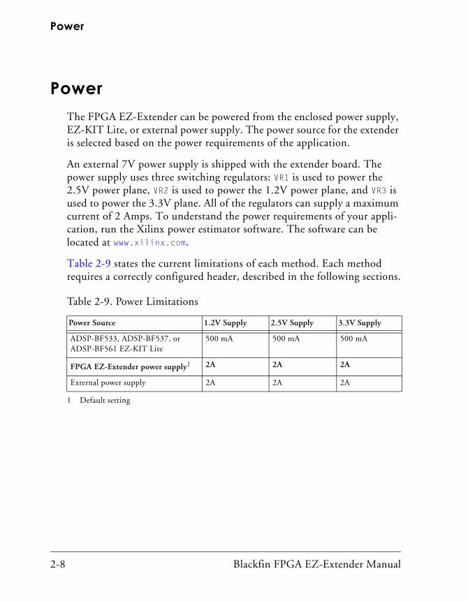
PowerThe FPGA EZ-Extender can be powered from the enclosed power supply, EZ-KIT Lite, or external power supply. The power source for the extender is selected based on the power requirements of the application.
An external 7V power supply is shipped with the extender board. The power supply uses three switching regulators: VR1 is used to power the 2.5V power plane, VR2 is used to power the 1.2V power plane, and VR3 is used to power the 3.3V plane. All of the regulators can supply a maximum current of 2 Amps. To understand the power requirements of your appli-cation, run the Xilinx power estimator software. The software can be located at www.xilinx.com.
Table 2-9 states the current limitations of each method. Each method requires a correctly configured header, described in the following sections.
Table 2-9. Power Limitations
Power Source 1.2V Supply 2.5V Supply 3.3V Supply
ADSP-BF533, ADSP-BF537, or ADSP-BF561 EZ-KIT Lite
500 mA 500 mA 500 mA
FPGA EZ-Extender power supply1
1 Default setting
2A 2A 2A
External power supply 2A 2A 2A
Blackfin FPGA EZ-Extender Manual 2-9
FPGA EZ-Extender Hardware Reference
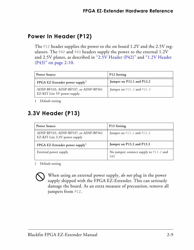
Power In Header (P12)The P12 header supplies the power to the on board 1.2V and the 2.5V reg-ulators. The P42 and P43 headers supply the power to the external 1.2V and 2.5V planes, as described in “2.5V Header (P42)” and “1.2V Header (P43)” on page 2-10.
3.3V Header (P13)
When using an external power supply, do not plug in the power supply shipped with the FPGA EZ-Extender. This can seriously damage the board. As an extra measure of precaution, remove all jumpers from P12.
Power Source P12 Setting
FPGA EZ-Extender power supply1
1 Default setting
Jumper on P12.1 and P12.2
ADSP-BF533, ADSP-BF537, or ADSP-BF561 EZ-KIT Lite 5V power supply
Jumper on P12.2 and P12.3
Power Source P13 Setting
ADSP-BF533, ADSP-BF537, or ADSP-BF561 EZ-KIT Lite 3.3V power supply
Jumper on P13.1 and P13.2
FPGA EZ-Extender power supply1
1 Default setting
Jumper on P13.2 and P13.3
External power supply No jumper; connect supply to P13.2 and GND
Power
2-10 Blackfin FPGA EZ-Extender Manual
2.5V Header (P42)
When using an external power supply, do not plug in the power supply shipped with the FPGA EZ-Extender. This can seriously damage the board. As an extra measure of precaution, remove all jumpers from P12.
1.2V Header (P43)
When using an external power supply, do not plug in the power supply shipped with the FPGA EZ-Extender. This can seriously damage the board. As an extra measure of precaution, remove all jumpers from P12.
Power Source P42 Setting
FPGA EZ-Extender Power Supply1
1 Default setting
No Jumper
External power supply Connect P42.1 to external 2.5VConnect P42.2 to external GND
Power Source P43 Setting
FPGA EZ-Extender power supply1
1 Default setting
No Jumper
External power supply Connect P42.1 to external 2.5VConnect P42.2 to external GND
Blackfin FPGA EZ-Extender Manual 2-11
FPGA EZ-Extender Hardware Reference
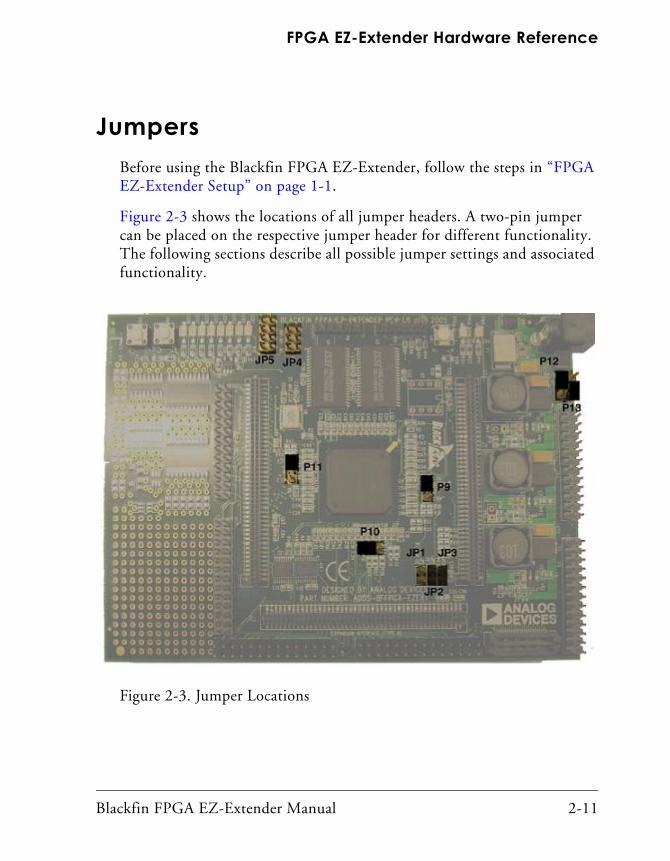
JumpersBefore using the Blackfin FPGA EZ-Extender, follow the steps in “FPGA EZ-Extender Setup” on page 1-1.
Figure 2-3 shows the locations of all jumper headers. A two-pin jumper can be placed on the respective jumper header for different functionality. The following sections describe all possible jumper settings and associated functionality.
Figure 2-3. Jumper Locations
Jumpers
2-12 Blackfin FPGA EZ-Extender Manual
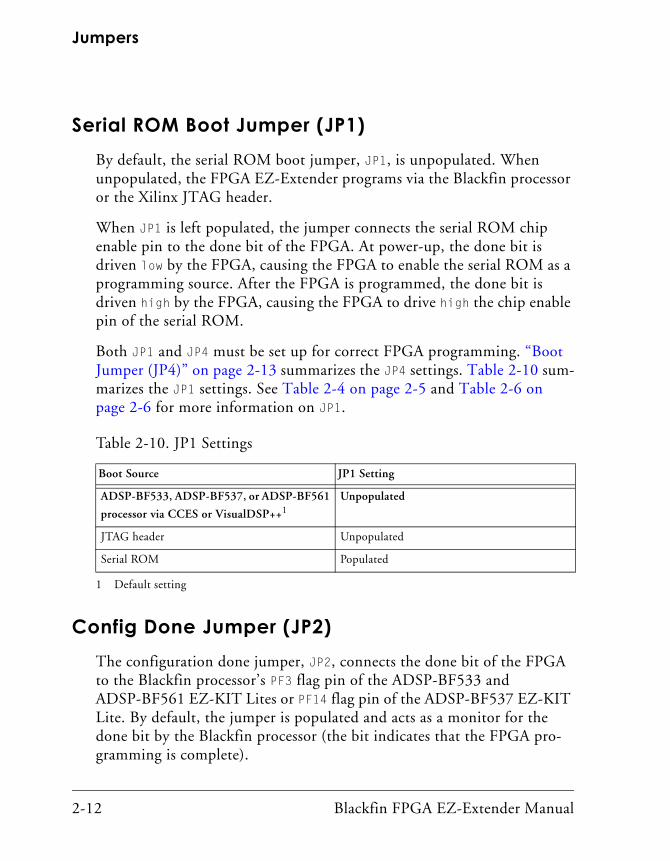
Serial ROM Boot Jumper (JP1)By default, the serial ROM boot jumper, JP1, is unpopulated. When unpopulated, the FPGA EZ-Extender programs via the Blackfin processor or the Xilinx JTAG header.
When JP1 is left populated, the jumper connects the serial ROM chip enable pin to the done bit of the FPGA. At power-up, the done bit is driven low by the FPGA, causing the FPGA to enable the serial ROM as a programming source. After the FPGA is programmed, the done bit is driven high by the FPGA, causing the FPGA to drive high the chip enable pin of the serial ROM.
Both JP1 and JP4 must be set up for correct FPGA programming. “Boot Jumper (JP4)” on page 2-13 summarizes the JP4 settings. Table 2-10 sum-marizes the JP1 settings. See Table 2-4 on page 2-5 and Table 2-6 on page 2-6 for more information on JP1.
Config Done Jumper (JP2)The configuration done jumper, JP2, connects the done bit of the FPGA to the Blackfin processor’s PF3 flag pin of the ADSP-BF533 and ADSP-BF561 EZ-KIT Lites or PF14 flag pin of the ADSP-BF537 EZ-KIT Lite. By default, the jumper is populated and acts as a monitor for the done bit by the Blackfin processor (the bit indicates that the FPGA pro-gramming is complete).
Table 2-10. JP1 Settings
Boot Source JP1 Setting
ADSP-BF533, ADSP-BF537, or ADSP-BF561
processor via CCES or VisualDSP++1
1 Default setting
Unpopulated
JTAG header Unpopulated
Serial ROM Populated
Blackfin FPGA EZ-Extender Manual 2-13
FPGA EZ-Extender Hardware Reference
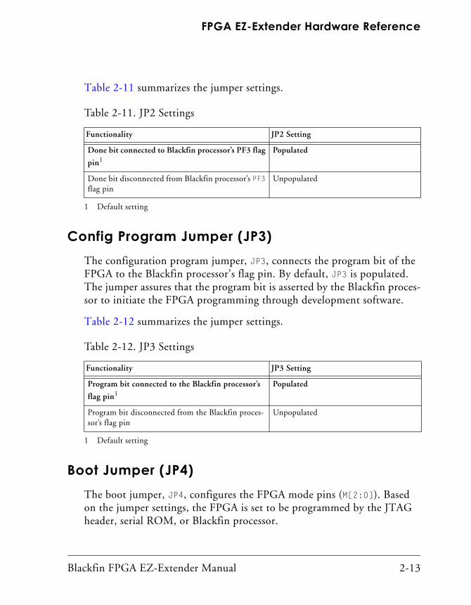
Table 2-11 summarizes the jumper settings.
Config Program Jumper (JP3)The configuration program jumper, JP3, connects the program bit of the FPGA to the Blackfin processor’s flag pin. By default, JP3 is populated. The jumper assures that the program bit is asserted by the Blackfin proces-sor to initiate the FPGA programming through development software.
Table 2-12 summarizes the jumper settings.
Boot Jumper (JP4)The boot jumper, JP4, configures the FPGA mode pins (M[2:0]). Based on the jumper settings, the FPGA is set to be programmed by the JTAG header, serial ROM, or Blackfin processor.
Table 2-11. JP2 Settings
Functionality JP2 Setting
Done bit connected to Blackfin processor’s PF3 flag
pin1
1 Default setting
Populated
Done bit disconnected from Blackfin processor’s PF3 flag pin
Unpopulated
Table 2-12. JP3 Settings
Functionality JP3 Setting
Program bit connected to the Blackfin processor’s
flag pin1
1 Default setting
Populated
Program bit disconnected from the Blackfin proces-sor’s flag pin
Unpopulated
Jumpers
2-14 Blackfin FPGA EZ-Extender Manual
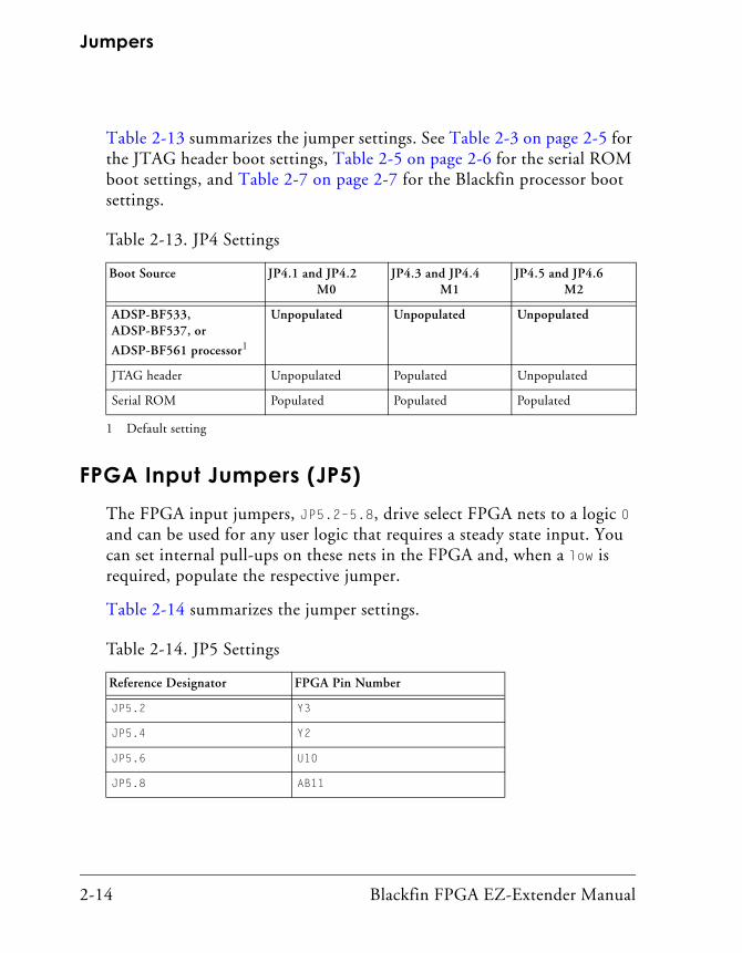
Table 2-13 summarizes the jumper settings. See Table 2-3 on page 2-5 for the JTAG header boot settings, Table 2-5 on page 2-6 for the serial ROM boot settings, and Table 2-7 on page 2-7 for the Blackfin processor boot settings.
FPGA Input Jumpers (JP5)The FPGA input jumpers, JP5.2–5.8, drive select FPGA nets to a logic 0 and can be used for any user logic that requires a steady state input. You can set internal pull-ups on these nets in the FPGA and, when a low is required, populate the respective jumper.
Table 2-14 summarizes the jumper settings.
Table 2-13. JP4 Settings
Boot Source JP4.1 and JP4.2M0
JP4.3 and JP4.4M1
JP4.5 and JP4.6M2
ADSP-BF533,ADSP-BF537, or
ADSP-BF561 processor1
1 Default setting
Unpopulated Unpopulated Unpopulated
JTAG header Unpopulated Populated Unpopulated
Serial ROM Populated Populated Populated
Table 2-14. JP5 Settings
Reference Designator FPGA Pin Number
JP5.2 Y3
JP5.4 Y2
JP5.6 U10
JP5.8 AB11
Blackfin FPGA EZ-Extender Manual 2-15
FPGA EZ-Extender Hardware Reference
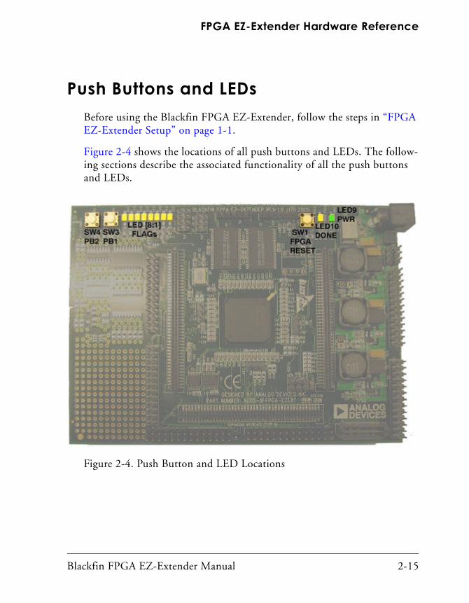
Push Buttons and LEDsBefore using the Blackfin FPGA EZ-Extender, follow the steps in “FPGA EZ-Extender Setup” on page 1-1.
Figure 2-4 shows the locations of all push buttons and LEDs. The follow-ing sections describe the associated functionality of all the push buttons and LEDs.
Figure 2-4. Push Button and LED Locations
Push Buttons and LEDs
2-16 Blackfin FPGA EZ-Extender Manual
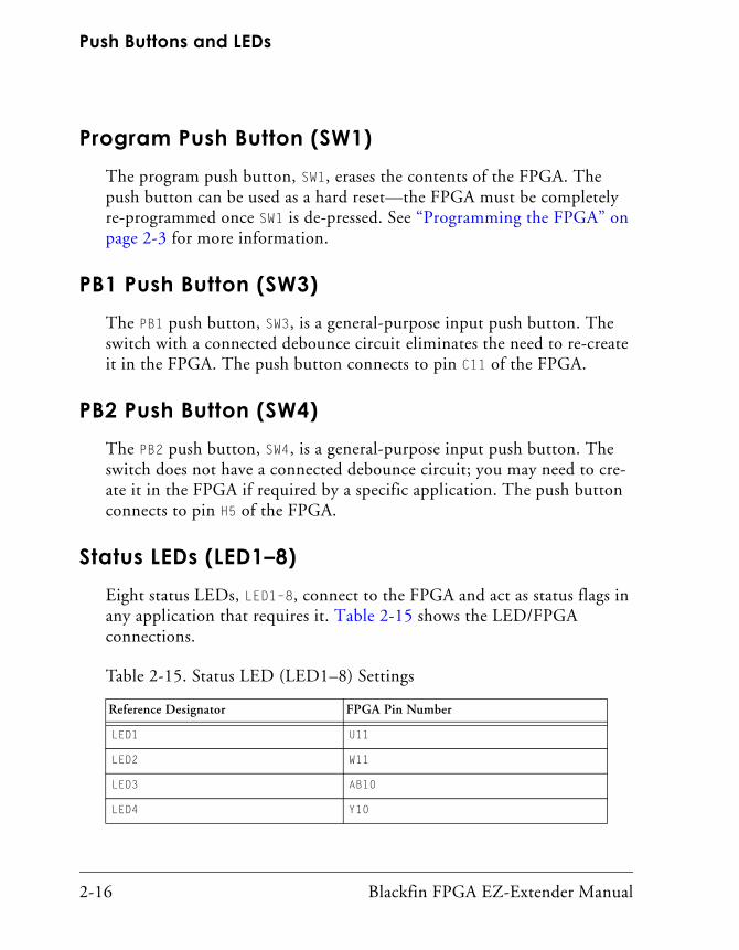
Program Push Button (SW1)The program push button, SW1, erases the contents of the FPGA. The push button can be used as a hard reset—the FPGA must be completely re-programmed once SW1 is de-pressed. See “Programming the FPGA” on page 2-3 for more information.
PB1 Push Button (SW3)The PB1 push button, SW3, is a general-purpose input push button. The switch with a connected debounce circuit eliminates the need to re-create it in the FPGA. The push button connects to pin C11 of the FPGA.
PB2 Push Button (SW4)The PB2 push button, SW4, is a general-purpose input push button. The switch does not have a connected debounce circuit; you may need to cre-ate it in the FPGA if required by a specific application. The push button connects to pin H5 of the FPGA.
Status LEDs (LED1–8)Eight status LEDs, LED1–8, connect to the FPGA and act as status flags in any application that requires it. Table 2-15 shows the LED/FPGA connections.
Table 2-15. Status LED (LED1–8) Settings
Reference Designator FPGA Pin Number
LED1 U11
LED2 W11
LED3 AB10
LED4 Y10
Blackfin FPGA EZ-Extender Manual 2-17
FPGA EZ-Extender Hardware Reference
Power LED (LED9)The power LED, LED9, connects to the 2.5V power supply and, when lit, signifies that the FPGA EZ-Extender is powered properly.
Done LED (LED10)The done LED, LED10, connects to the done pin of the FPGA. At power-up, the FPGA is blank and needs to be programmed. When lit, the LED indicates that the FPGA is programmed successfully.
ConnectorsBefore using the Blackfin FPGA EZ-Extender, follow the steps in “FPGA EZ-Extender Setup” on page 1-1.
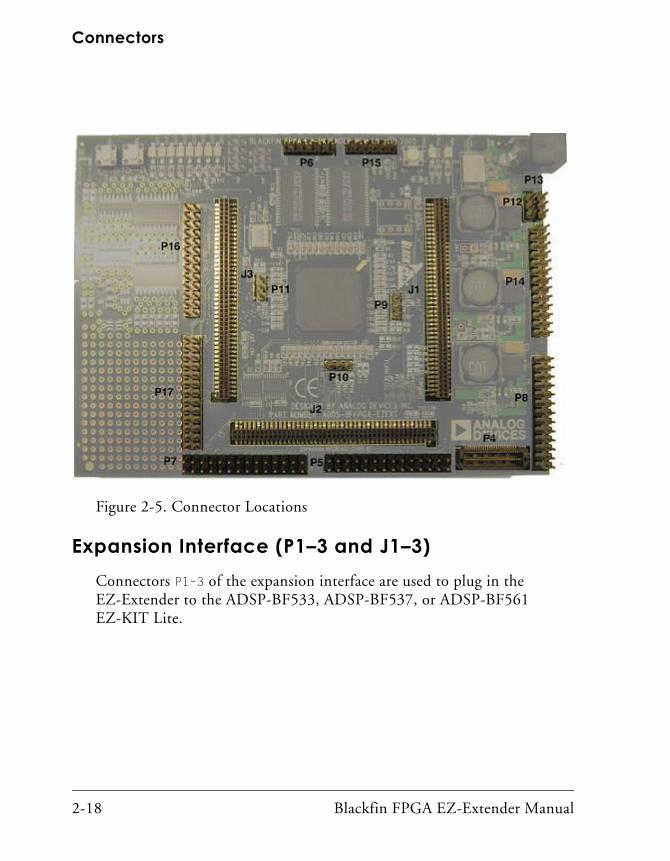
This section describes the connector functionality and provides informa-tion about the mating connectors. The connector locations are shown in Figure 2-5.
LED5 AB9
LED6 W9
LED7 AB8
LED8 V10
Table 2-15. Status LED (LED1–8) Settings (Cont’d)
Reference Designator FPGA Pin Number
Connectors
2-18 Blackfin FPGA EZ-Extender Manual
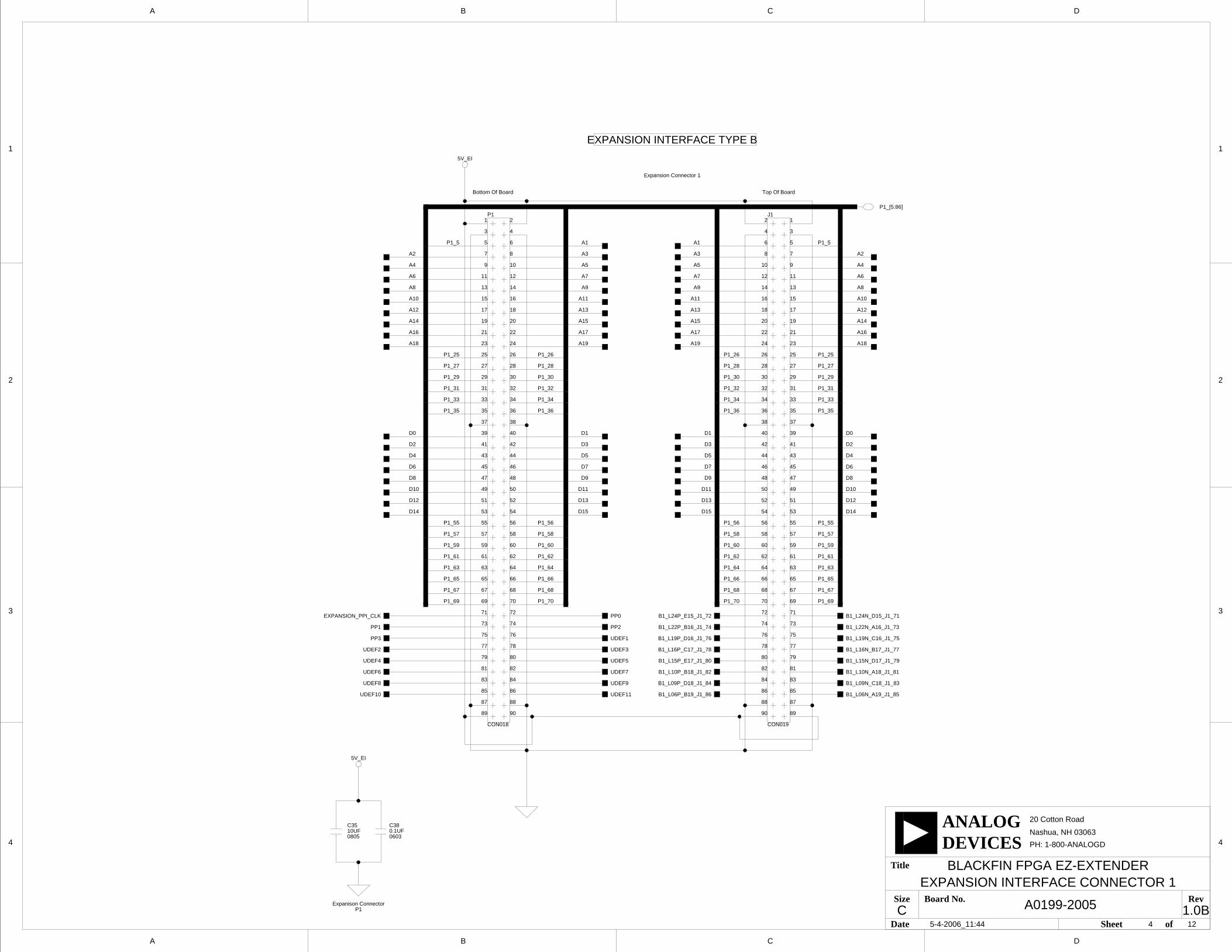
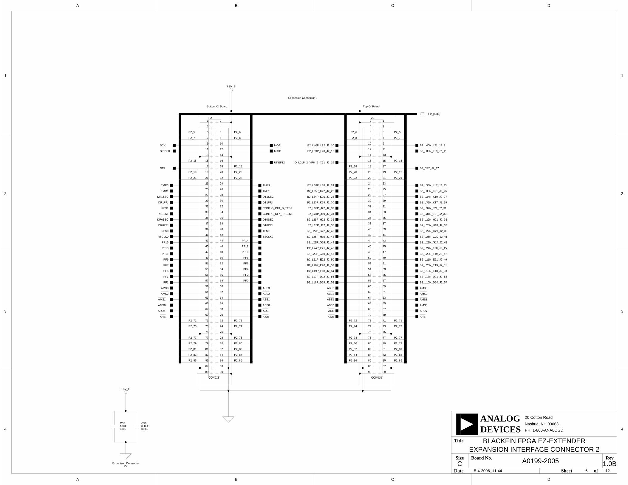
Expansion Interface (P1–3 and J1–3)Connectors P1–3 of the expansion interface are used to plug in the EZ-Extender to the ADSP-BF533, ADSP-BF537, or ADSP-BF561 EZ-KIT Lite.
Figure 2-5. Connector Locations
Blackfin FPGA EZ-Extender Manual 2-19
FPGA EZ-Extender Hardware Reference
Connectors J1–3 of the expansion interface are used to plug in another extender board, such as the Blackfin USB-LAN EZ-Extender. Your own custom board can be plugged into J1–3 as well.
Plugging in another EZ-Extender or a customer board to the expansion interface can de-grade the overall system performance. The extra overall load can cause the user to add wait states or slow down the system bus to get all of the boards to work properly.
For the J1–3 and P1–3 connector availability and pricing, contact Samtec.
IDC Connectors (P8, P14, P16, and P17)The P8, P14, P16, and P17 connectors are standard 0.1” IDC headers. The connectors are in a 13 x 2 configuration and designed for signal probing, bread boarding, and other signal accesses.
Part Description Manufacturer Part Number
90-position 0.05” spacing, SMT(J1, J2, J3)
Samtec SFC-145-T2-F-D-A
90-position 0.05” spacing (P1, P2, P3)
Samtec TFC-145-32-F-D
Part Description Manufacturer Part Number
IDC13x2 0.1” header Berg 54102-T08-13
Mating Connector
IDC 13x2 0.1” plug Samtec SSW-113-01-T-D
Connectors
2-20 Blackfin FPGA EZ-Extender Manual
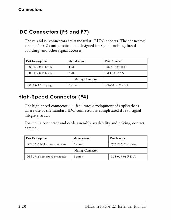
IDC Connectors (P5 and P7)The P5 and P7 connectors are standard 0.1” IDC headers. The connectors are in a 14 x 2 configuration and designed for signal probing, bread boarding, and other signal accesses.
High-Speed Connector (P4)The high-speed connector, P4, facilitates development of applications where use of the standard IDC connectors is complicated due to signal integrity issues.
For the P4 connector and cable assembly availability and pricing, contact Samtec.
Part Description Manufacturer Part Number
IDC14x2 0.1” header FCI 68737-428HLF
IDC14x2 0.1” header Sullins GEC14DAAN
Mating Connector
IDC 14x2 0.1” plug Samtec SSW-114-01-T-D
Part Description Manufacturer Part Number
QTS 25x2 high-speed connector Samtec QTS-025-01-F-D-A
Mating Connector
QSS 25x2 high-speed connector Samtec QSS-025-01-F-D-A
Blackfin FPGA EZ-Extender Manual A-1
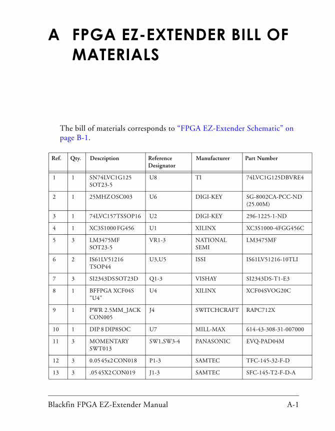
A FPGA EZ-EXTENDER BILL OF MATERIALS
The bill of materials corresponds to “FPGA EZ-Extender Schematic” on page B-1.
Ref. Qty. Description Reference Designator
Manufacturer Part Number
1 1 SN74LVC1G125 SOT23-5
U8 TI 74LVC1G125DBVRE4
2 1 25MHZ OSC003 U6 DIGI-KEY SG-8002CA-PCC-ND(25.00M)
3 1 74LVC157 TSSOP16 U2 DIGI-KEY 296-1225-1-ND
4 1 XC3S1000 FG456 U1 XILINX XC3S1000-4FGG456C
5 3 LM3475MF SOT23-5
VR1-3 NATIONAL SEMI
LM3475MF
6 2 IS61LV51216 TSOP44
U3,U5 ISSI IS61LV51216-10TLI
7 3 SI2343DS SOT23D Q1-3 VISHAY SI2343DS-T1-E3
8 1 BFFPGA XCF04S "U4"
U4 XILINX XCF04SVOG20C
9 1 PWR 2.5MM_JACK CON005
J4 SWITCHCRAFT RAPC712X
10 1 DIP 8 DIP8SOC U7 MILL-MAX 614-43-308-31-007000
11 3 MOMENTARY SWT013
SW1,SW3-4 PANASONIC EVQ-PAD04M
12 3 0.05 45x2 CON018 P1-3 SAMTEC TFC-145-32-F-D
13 3 .05 45X2 CON019 J1-3 SAMTEC SFC-145-T2-F-D-A
A-2 Blackfin FPGA EZ-Extender Manual
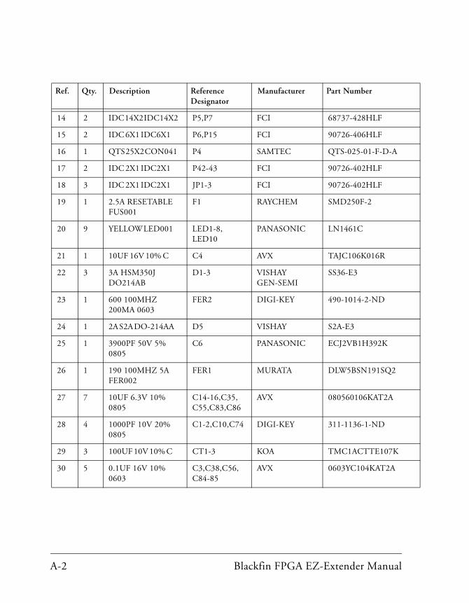
14 2 IDC 14X2 IDC14X2 P5,P7 FCI 68737-428HLF
15 2 IDC 6X1 IDC6X1 P6,P15 FCI 90726-406HLF
16 1 QTS 25X2 CON041 P4 SAMTEC QTS-025-01-F-D-A
17 2 IDC 2X1 IDC2X1 P42-43 FCI 90726-402HLF
18 3 IDC 2X1 IDC2X1 JP1-3 FCI 90726-402HLF
19 1 2.5A RESETABLE FUS001
F1 RAYCHEM SMD250F-2
20 9 YELLOW LED001 LED1-8,LED10
PANASONIC LN1461C
21 1 10UF 16V 10% C C4 AVX TAJC106K016R
22 3 3A HSM350J DO214AB
D1-3 VISHAY GEN-SEMI
SS36-E3
23 1 600 100MHZ 200MA 0603
FER2 DIGI-KEY 490-1014-2-ND
24 1 2A S2A DO-214AA D5 VISHAY S2A-E3
25 1 3900PF 50V 5% 0805
C6 PANASONIC ECJ2VB1H392K
26 1 190 100MHZ 5A FER002
FER1 MURATA DLW5BSN191SQ2
27 7 10UF 6.3V 10% 0805
C14-16,C35,C55,C83,C86
AVX 080560106KAT2A
28 4 1000PF 10V 20% 0805
C1-2,C10,C74 DIGI-KEY 311-1136-1-ND
29 3 100UF 10V 10% C CT1-3 KOA TMC1ACTTE107K
30 5 0.1UF 16V 10% 0603
C3,C38,C56, C84-85
AVX 0603YC104KAT2A
Ref. Qty. Description Reference Designator
Manufacturer Part Number
Blackfin FPGA EZ-Extender Manual A-3
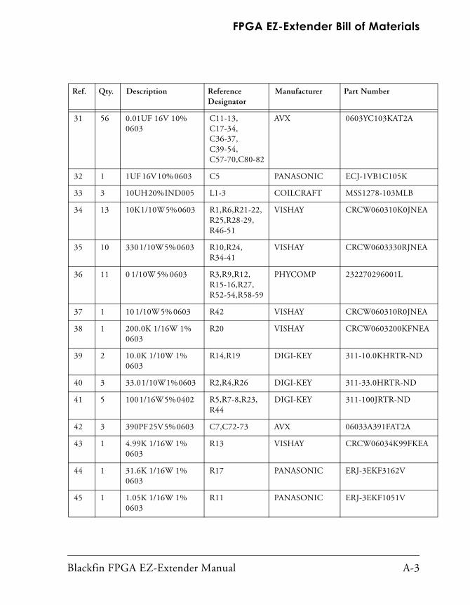
FPGA EZ-Extender Bill of Materials
31 56 0.01UF 16V 10% 0603
C11-13,C17-34,C36-37,C39-54,C57-70,C80-82
AVX 0603YC103KAT2A
32 1 1UF 16V 10% 0603 C5 PANASONIC ECJ-1VB1C105K
33 3 10UH 20% IND005 L1-3 COILCRAFT MSS1278-103MLB
34 13 10K 1/10W 5% 0603 R1,R6,R21-22,R25,R28-29,R46-51
VISHAY CRCW060310K0JNEA
35 10 330 1/10W 5% 0603 R10,R24,R34-41
VISHAY CRCW0603330RJNEA
36 11 0 1/10W 5% 0603 R3,R9,R12,R15-16,R27,R52-54,R58-59
PHYCOMP 232270296001L
37 1 10 1/10W 5% 0603 R42 VISHAY CRCW060310R0JNEA
38 1 200.0K 1/16W 1% 0603
R20 VISHAY CRCW0603200KFNEA
39 2 10.0K 1/10W 1% 0603
R14,R19 DIGI-KEY 311-10.0KHRTR-ND
40 3 33.0 1/10W 1% 0603 R2,R4,R26 DIGI-KEY 311-33.0HRTR-ND
41 5 100 1/16W 5% 0402 R5,R7-8,R23,R44
DIGI-KEY 311-100JRTR-ND
42 3 390PF 25V 5% 0603 C7,C72-73 AVX 06033A391FAT2A
43 1 4.99K 1/16W 1% 0603
R13 VISHAY CRCW06034K99FKEA
44 1 31.6K 1/16W 1% 0603
R17 PANASONIC ERJ-3EKF3162V
45 1 1.05K 1/16W 1% 0603
R11 PANASONIC ERJ-3EKF1051V
Ref. Qty. Description Reference Designator
Manufacturer Part Number
A-4 Blackfin FPGA EZ-Extender Manual
46 1 2.15K 1/16W 1% 0603
R18 VISHAY CRCW06032K15FKEA
47 3 10UF 10V 10% 0805 C8-9,C71 PANASONIC ECJ-2FB1A106K
Ref. Qty. Description Reference Designator
Manufacturer Part Number
D
4
3
2
1
A B C
20 Cotton Road
Nashua, NH 03063
A B C D
4
3
2
1
PH: 1-800-ANALOGD
C
Title
Size Board No.
Date Sheet of
DEVICESANALOG
Rev
BLACKFIN FPGA EZ-EXTENDER
A0199-2005 1.0B
SchematicBLACKFIN FPGA EZ-EXTENDER
5-4-2006_11:44 1 12
TITLE
3.3V
3.3V
D
4
3
2
1
A B C
20 Cotton Road
Nashua, NH 03063
A B C D
4
3
2
1
PH: 1-800-ANALOGD
C
Title
Size Board No.
Date Sheet of
DEVICESANALOG
Rev
BLACKFIN FPGA EZ-EXTENDER
A0199-2005 1.0B
1A
1B
1Y
2A
2B
2Y
3A
3B
3Y
4A
4B
4Y
~A/B
EN
2.5V
3.3V
3.3V
3.3V
3.3V
3.3V
2.5V
3.3V
3.3V
OE/NC OUT
VCCAUX_A6
VCCAUX_A17
VCCAUX_F1
VCCAUX_F22
VCCAUX_U1
VCCAUX_U22
VCCAUX_AB6
VCCAUX_AB17
VCCINT_G7
VCCINT_G8
VCCINT_G15
VCCINT_G16
VCCINT_H7
VCCINT_H16
VCCINT_R7
VCCINT_R16
VCCINT_T7
VCCINT_T8
VCCINT_T15
VCCINT_T16
TCK
TDI
TDO
TMS
M0
M1
M2
CCLK
PROG_B
DONE
HSWAP_EN
GND_A1
GND_A22
GND_B2
GND_B21
GND_C9
GND_C14
GND_J3
GND_J9
GND_J10
GND_J11
GND_J12
GND_J13
GND_J14
GND_J20
GND_K9
GND_K10
GND_K11
GND_K12
GND_K13
GND_K14
GND_L9
GND_L10
GND_L11
GND_L12
GND_L13
GND_L14
GND_M9
GND_M10
GND_M11
GND_M12
GND_M13
GND_M14
GND_N9
GND_N10
GND_N11
GND_N12
GND_N13
GND_N14
GND_P3
GND_P9
GND_P10
GND_P11
GND_P12
GND_P13
GND_P14
GND_P20
GND_Y9
GND_Y14
GND_AA2
GND_AA21
GND_AB1
GND_AB22
CF
CEO
CE
VCCO
VCCJ
VCCINT
TMS
TDO
TDI
TCK
OE/~RESET
NC6
NC5
NC4
NC3
NC2
NC1
GND
D0
CLK
GNDOE OUT
VDD
FPGAFPGA
EXTRA CLOCK SOCKET
FPGA JTAG HEADER
BOOTMODE JUMPER
FPGA BOOT FLASH(2Mbit)
MUXFLASHSKTOSC
25MHZ SYSTEM CLOCK
FLASH JTAG HEADER
1225-4-2006_11:44
R433.00603
2
1 3
4
25MHZOSC003
U6
7
13
10
19
20
18
5
17
4
6
8
16
15
14
12
9
2
11
1
3
XCF04STSSOP20
U4
A6
A17
F1
F22
U1
U22
AB6
AB17
G7
G8
G15
G16
H7
H16
R7
R16
T7
T8
T15
T16
A21
B1
B22
A20
AB2
AA1
AB3
AA22
A2
AB21
B3
A1
A22
B2
B21
C9
C14
J3
J9
J10
J11
J12
J13
J14
J20
K9
K10
K11
K12
K13
K14
L9
L10
L11
L12
L13
L14
M9
M10
M11
M12
M13
M14
N9
N10
N11
N12
N13
N14
P3
P9
P10
P11
P12
P13
P14
P20
Y9
Y14
AA2
AA21
AB1
AB22
U1
FG456XC3S1000
6
5
4
3
2
1P6
IDC6X1
1 5U7
DIPDIP8SOC
R2510K0603DNP
FLASH_DONE
060333.0R2
CONFIG_PROG_B
1
2
3
4
5
6
P15
IDC6X1
2
4
5 6
3
1JP4
IDC3X2
0402100R5
0402100R44
R81000402
R71000402
080510UFC14
R29
060310K
R22
060310K
R21
060310K
R1
060310K
R2633.00603
1.2V
1 2JP1
IDC2X1
CONFIG_DONER3
06030
CONFIG_CLK_TSCLK1
FPGA_TMS
FPGA_TDO
FPGA_TCK
FPGA_TDI
FPGA_TCK
FPGA_TDO
FPGA_TDI
FPGA_TMS
FLASH_TMS
FLASH_TDI
FLASH_TDO
FLASH_TCK
M1
M2
M0
1.2V
MOMENTARYSWT013SW1
2
3
4
5
6
7
11
10
9
14
13
12
1
15
U2
TSSOP1674LVC157
CONFIG_DONE
FLASH_TMS
FLASH_TCK
FLASH_TDI
FLASH_TDO
M2
M0
M1
FPGA CONFIG
CONFIG_INIT_B_TFS1
FLASH_DOUT
CONFIG_CLK_TSCLK1
FLASH_DONE
0.01UF0603
C18
IO_L32_0_GCLK6_A11B4_L32N_GCKL1_AA12
C19
06030.01UF 0.01UF
0603
C20 C21
06030.01UF 0.01UF
0603
C25C24
06030.01UF0.01UF
0603
C23C22
06030.01UF 0.01UF
0603
C31 C30
06030.01UF 0.01UF
0603
C29 C28
06030.01UF0.01UF
0603
C27C26
06030.01UF
0.01UF0603
C32 C11
06030.01UF 0.01UF
0603
C12 C13
06030.01UF
080510UFC15 C16
10UF0805
C17
06030.01UF
0603330R24
LED10
LED001YELLOW
CONFIG_DIN_DT1PRI
FLASH_DOUT
DT1PRI
R6
060310K10K
0603
R28
3.3V 3.3V
D
4
3
2
1
A B C
20 Cotton Road
Nashua, NH 03063
A B C D
4
3
2
1
PH: 1-800-ANALOGD
C
Title
Size Board No.
Date Sheet of
DEVICESANALOG
Rev
BLACKFIN FPGA EZ-EXTENDER
A0199-2005 1.0B
3.3V
3.3V
A18
A1
A10
A11
A12
A13
A14
A16
A2
A3
A4
A5
A6
A7
A8
A9
D0
D1
D10
D11
D2
D3
D4
D5
D6
D7
D8
D9
BHE
BLE
CE
OE
WE
A17
D15
D14
D13
D12
A0
A15
VCCO_6_M7
VCCO_6_N7
VCCO_6_P7
VCCO_6_R3
VCCO_6_R6
IO_Y1
IO_L16N_6_W4
IO_L16P_6_W3
IO_L17N_6_W2
IO_L17P_6_VREF_6_W1
IO_L19N_6_V5
IO_L19P_6_U5
IO_L20N_6_V4
IO_L20P_6_V3
IO_L21N_6_V2
IO_L21P_6_V1
IO_L22N_6_T6
IO_L22P_6_T5
IO_L23N_6_U4
IO_L23P_6_T4
IO_L24N_6_VREF_6_U3
IO_L24P_6_U2
IO_L26N_6_T3
IO_L26P_6_R4
IO_L27N_6_T2
IO_L27P_6_T1
IO_L28N_6_R5
IO_L28P_6_P6
IO_L29N_6_R2
IO_L29P_6_R1
IO_L31N_6_P5
IO_L31P_6_P4
IO_L32N_6_P2
IO_L32P_6_P1
IO_L33N_6_N6
IO_L33P_6_N5
IO_L34N_6_VREF_6_N4
IO_L34P_6_N3
IO_L35N_6_N2
IO_L35P_6_N1
IO_L38N_6_M6
IO_L38P_6_M5
IO_L39N_6_M4
IO_L39P_6_M3
IO_L40N_6_M2
IO_L40P_6_VREF_6_M1
IO_L01N_6_VRP_6_Y3
IO_L01P_6_VRN_6_Y2
VCCO_7_H3
VCCO_7_H6
VCCO_7_J7
VCCO_7_K7
VCCO_7_L7
IO_C2
IO_L16N_7_D1
IO_L16P_7_VREF_7_C1
IO_L17N_7_E4
IO_L17P_7_D4
IO_L19N_7_VREF_7_D3
IO_L19P_7_D2
IO_L20N_7_F4
IO_L20P_7_E3
IO_L21N_7_E1
IO_L21P_7_E2
IO_L22N_7_G6
IO_L22P_7_F5
IO_L23N_7_F2
IO_L23P_7_F3
IO_L24N_7_H5
IO_L24P_7_G5
IO_L26N_7_G3
IO_L26P_7_G4
IO_L27N_7_G1
IO_L27P_7_VREF_7_G2
IO_L28N_7_H1
IO_L28P_7_H2
IO_L29N_7_J4
IO_L29P_7_H4
IO_L31N_7_J5
IO_L31P_7_J6
IO_L32N_7_J1
IO_L32P_7_J2
IO_L33N_7_K5
IO_L33P_7_K6
IO_L34N_7_K3
IO_L34P_7_K4
IO_L35N_7_K1
IO_L35P_7_K2
IO_L38N_7_L5
IO_L38P_7_L6
IO_L39N_7_L3
IO_L39P_7_L4
IO_L40N_7_VREF_7_L1
IO_L40P_7_L2
IO_L01N_7_VRP_7_C3
IO_L01P_7_VRN_7_C4
A18
A1
A10
A11
A12
A13
A14
A16
A2
A3
A4
A5
A6
A7
A8
A9
D0
D1
D10
D11
D2
D3
D4
D5
D6
D7
D8
D9
BHE
BLE
CE
OE
WE
A17
D15
D14
D13
D12
A0
A15
(512k x 16bits x 2chips)
FPGASRAM SRAM
2MBYTES FPGA SRAM
1235-4-2006_11:44
42
1
35
36
37
38
44
17
41
6
39
40
30
29
16
15
14
13
10
9
32
31
8
7
22
21
20
19
18
5
4
3
43
27
26
25
24
23
2
28
U5
TSOP44IS61LV51216
SRAM_A9
FLASH_TDO
FLASH_TMS
FLASH_TDI
FLASH_TCK
M7
N7
P7
R3
R6
Y1
W4
W3
W2
W1
V5
U5
V4
V3
V2
V1
T6
T5
U4
T4
U3
U2
T3
R4
T2
T1
R5
P6
R2
R1
P5
P4
P2
P1
N6
N5
N4
N3
N2
N1
M6
M5
M4
M3
M2
M1
Y3
Y2
H3
H6
J7
K7
L7
C2
D1
C1
E4
D4
D3
D2
F4
E3
E1
E2
G6
F5
F2
F3
H5
G5
G3
G4
G1
G2
H1
H2
J4
H4
J5
J6
J1
J2
K5
K6
K3
K4
K1
K2
L5
L6
L3
L4
L1
L2
C3
C4
U1
FG456XC3S1000
28
2
23
24
25
26
27
43
3
4
5
18
19
20
21
22
7
8
31
32
9
10
13
14
15
16
29
30
40
39
6
41
17
44
38
37
36
35
1
42
U3
TSOP44IS61LV51216
SRAM_D7
SRAM_D6
SRAM_D3
SRAM_D2
SRAM_D0
SRAM_D8
SRAM_D9
SRAM_D5
SRAM_D4
SRAM_D13
SRAM_D1
SRAM_D10
SRAM_D11
SRAM_D12
SRAM_D14
SRAM_D15
SRAM_CE
SRAM_A7
SRAM_A0
SRAM_A5
SRAM_A3
SRAM_A1
SRAM_WE
SRAM_A8
SRAM_A6
SRAM_A4
SRAM_A2
SRAM_A17
SRAM_OE
SRAM_A12
SRAM_A13
SRAM_A15
SRAM_A16
SRAM_A14
SRAM_A18
SRAM_A11
SRAM_A10
SRAM_D22
SRAM_D20
SRAM_D18
SRAM_D17
SRAM_D16
SRAM_D26
SRAM_D21
SRAM_D24
SRAM_D19
SRAM_D31
SRAM_D25
SRAM_D27
SRAM_D28
SRAM_D30
SRAM_D29
PB2
A11
A5
D1
A15
A3
A9
D13
D7
A13
A19
A7
A1
A18
A6
A2
A12
D6
A8
A14
D2
D0
A10
A4
D3
A16
SRAM, FPGA BANKS 7 + 8
SRAM_CE
SRAM_WE
SRAM_OE
SRAM_A18
SRAM_A0 SRAM_D0
SRAM_D1
SRAM_D2
SRAM_D3
SRAM_D4
SRAM_D5
SRAM_D6
SRAM_D7
SRAM_D8
SRAM_D9
SRAM_D10
SRAM_D11
SRAM_D12
SRAM_D13
SRAM_D14
SRAM_D15
SRAM_D16
SRAM_D17
SRAM_D18
SRAM_D19
SRAM_D20
SRAM_D21
SRAM_D22
SRAM_D23
SRAM_D24
SRAM_D25
SRAM_D26
SRAM_D27
SRAM_D28
SRAM_D29
SRAM_D30
SRAM_D31
SRAM_A1
SRAM_A2
SRAM_A3
SRAM_A4
SRAM_A5
SRAM_A6
SRAM_A7
SRAM_A8
SRAM_A9
SRAM_A10
SRAM_A11
SRAM_A12
SRAM_A13
SRAM_A14
SRAM_A15
SRAM_A16
SRAM_A17
SRAM_A1
SRAM_A2
SRAM_A3
SRAM_A4
SRAM_A5
SRAM_A6
SRAM_A7
SRAM_A8
SRAM_A9
SRAM_A10
SRAM_A11
SRAM_A12
SRAM_A13
SRAM_A14
SRAM_A15
SRAM_A16
SRAM_A17
SRAM_A18
SRAM_A0
SRAM_OE
SRAM_WE
SRAM_CE
C33
06030.01UF
C34
06030.01UF0.01UF
0603
C370.01UF0603
C36
C42
06030.01UF 0.01UF
0603
C41 C40
06030.01UF0.01UF
0603
C390.01UF0603
C46 C45
06030.01UF 0.01UF
0603
C44C43
06030.01UF
B6_L01P_Y2
B6_L01N_Y3
SRAM_D23
D
4
3
2
1
A B C
20 Cotton Road
Nashua, NH 03063
A B C D
4
3
2
1
PH: 1-800-ANALOGD
C
Title
Size Board No.
Date Sheet of
DEVICESANALOG
Rev
BLACKFIN FPGA EZ-EXTENDER
A0199-2005 1.0B
EXPANSION INTERFACE TYPE B
P1Expanison Connector
Top Of BoardBottom Of Board
Expansion Connector 1
5-4-2006_11:44 4 12
EXPANSION INTERFACE CONNECTOR 1
C3510UF0805
0.1UF0603
C38
5V_EI
5V_EI
1
10
11 12
13 14
15 16
17 18
19
2
20
21 22
23 24
25 26
27 28
29
3
30
31 32
33 34
35 36
37 38
39
4
40
41 42
43 44
45 46
47 48
49
5
50
51 52
53 54
55 56
57 58
59
6
60
61 62
63 64
65 66
67 68
69
7
70
71 72
73 74
75 76
77 78
79
8
80
81 82
83 84
85 86
87 88
89
9
90
P1
CON018
1
10
1112
1314
1516
1718
19
2
20
2122
2324
2526
2728
29
3
30
3132
3334
3536
3738
39
4
40
4142
4344
4546
4748
49
5
50
5152
5354
5556
5758
59
6
60
6162
6364
6566
6768
69
7
70
7172
7374
7576
7778
79
8
80
8182
8384
8586
8788
89
9
90
J1
CON019
PP1
EXPANSION_PPI_CLK
PP3
UDEF2
UDEF4
UDEF6
UDEF8
UDEF10
D9
D7
D15
D13
D11
D5
D1
D3
D15
D9
D5
D1
D3
D0
D2
D4
D6
D8
D10
D14
D12
P1_5
P1_25
P1_27
P1_29
P1_31
P1_33
P1_55
P1_57
P1_59
P1_61
P1_63
P1_65
P1_67
P1_69
P1_35
P1_26
P1_28
P1_30
P1_32
P1_34
P1_56
P1_58
P1_60
P1_62
P1_64
P1_66
P1_68
P1_70
P1_36
P1_26
P1_28
P1_30
P1_32
P1_34
P1_36
P1_56
P1_58
P1_60
P1_62
P1_64
P1_66
P1_68
P1_70
P1_5
P1_25
P1_27
P1_29
P1_31
P1_33
P1_35
P1_55
P1_57
P1_59
P1_61
P1_63
P1_65
P1_67
P1_69
P1_[5:86]
A5
A6A7
A8A9
A10A11
A12A13
A14A15
A16A17
A18A19
D0
D2
D4
D6D7
D8
D10D11
D12D13
D14
A1
A2
B1_L24N_D15_J1_71B1_L24P_E15_J1_72
B1_L22N_A16_J1_73B1_L22P_B16_J1_74
B1_L19N_C16_J1_75B1_L19P_D16_J1_76
B1_L16N_B17_J1_77B1_L16P_C17_J1_78
B1_L15N_D17_J1_79
A3
B1_L15P_E17_J1_80
B1_L10N_A18_J1_81B1_L10P_B18_J1_82
B1_L09N_C18_J1_83B1_L09P_D18_J1_84
B1_L06N_A19_J1_85B1_L06P_B19_J1_86
A4A5
A6 A7
A8 A9
A10 A11
A12 A13
A14 A15
A16 A17
A18 A19
A1
A2
PP0
PP2
UDEF1
UDEF3
A3
UDEF5
UDEF7
UDEF9
UDEF11
A4
3.3V
2.5V 3.3V
3.3V
3.3V
3.3V
D
4
3
2
1
A B C
20 Cotton Road
Nashua, NH 03063
A B C D
4
3
2
1
PH: 1-800-ANALOGD
C
Title
Size Board No.
Date Sheet of
DEVICESANALOG
Rev
BLACKFIN FPGA EZ-EXTENDER
A0199-2005 1.0B
VCCO_0_C8
VCCO_0_F8
VCCO_0_G9
VCCO_0_G10
VCCO_0_G11
IO_A10
IO_D9
IO_D10
IO_F6
IO_VREF_0_A3
IO_VREF_0_C7
IO_VREF_0_E5
IO_VREF_0_F7
IO_L06N_0_D5
IO_L06P_0_C5
IO_L09N_0_B5
IO_L09P_0_A5
IO_L10N_0_E6
IO_L10P_0_D6
IO_L15N_0_C6
IO_L15P_0_B6
IO_L16N_0_E7
IO_L16P_0_D7
IO_L19N_0_B7
IO_L19P_0_A7
IO_L22N_0_E8
IO_L22P_0_D8
IO_L24N_0_B8
IO_L24P_0_A8
IO_L25N_0_F9
IO_L25P_0_E9
IO_L27N_0_B9
IO_L27P_0_A9
IO_L28N_0_F10
IO_L28P_0_E10
IO_L29N_0_C10
IO_L29P_0_B10
IO_L30N_0_F11
IO_L30P_0_E11
IO_L31N_0_D11
IO_L31P_0_VREF_0_C11
IO_L01N_0_VRP_0_B4
IO_L01P_0_VRN_0_A4
IO_L32N_0_GCLK7_B11
IO_L32P_0_GCLK6_A11
VCCO_1_C15
VCCO_1_F15
VCCO_1_G12
VCCO_1_G13
VCCO_1_G14
IO_A12
IO_E16
IO_F12
IO_F13
IO_F16
IO_F17
IO_VREF_1_E13
IO_VREF_1_F14
IO_L06N_1_VREF_1_A19
IO_L06P_1_B19
IO_L09N_1_C18
IO_L09P_1_D18
IO_L10N_1_VREF_1_A18
IO_L10P_1_B18
IO_L15N_1_D17
IO_L15P_1_E17
IO_L16N_1_B17
IO_L16P_1_C17
IO_L19N_1_C16
IO_L19P_1_D16
IO_L22N_1_A16
IO_L22P_1_B16
IO_L24N_1_D15
IO_L24P_1_E15
IO_L25N_1_B15
IO_L25P_1_A15
IO_L27N_1_D14
IO_L27P_1_E14
IO_L28N_1_A14
IO_L28P_1_B14
IO_L29N_1_C13
IO_L29P_1_D13
IO_L30N_1_A13
IO_L30P_1_B13
IO_L31N_1_VREF_1_D12
IO_L31P_1_E12
IO_L01N_1_VRP_1_C19
IO_L01P_1_VRN_1_B20
IO_L32N_1_GCLK5_B12
IO_L32P_1_GCLK4_C12
FPGAFPGA
LAYOUT NOTE: PLACE NEAR FPGA
5 125-4-2006_11:44
C8
F8
G9
G10
G11
A10
D9
D10
F6
A3
C7
E5
F7
D5
C5
B5
A5
E6
D6
C6
B6
E7
D7
B7
A7
E8
D8
B8
A8
F9
E9
B9
A9
F10
E10
C10
B10
F11
E11
D11
C11
B4
A4
B11
A11
C15
F15
G12
G13
G14
A12
E16
F12
F13
F16
F17
E13
F14
A19
B19
C18
D18
A18
B18
D17
E17
B17
C17
C16
D16
A16
B16
D15
E15
B15
A15
D14
E14
A14
B14
C13
D13
A13
B13
D12
E12
C19
B20
B12
C12
U1
FG456XC3S1000
R51
060310K
DNP
10K0603
R50
DNP
10K0603
R48
DNP
R49
060310K
DNP
00603
R54
DNP
R53
06030
DNP
00603
R52
DNP
EXPANSION_PPI_CLK
B1_L10N_A18_J1_81
B1_L16P_C17_J1_78
B1_L16N_B17_J1_77
R31
060349.9
DNP
49.90603
R30
DNP
1
10
11 12
13 14
15 16
17 18
19
2
20
21 22
23 24
25 26
27 28
29
3
30
31 32
33 34
35 36
37 38
4
5 6
7 8
9
39 40
41
43
45
47
49
42
44
46
48
50
CON041
P4
5
1
18
20
22
26
24
16
14
12
25
23
21
19
17
15
13
11
9
3
6
10
8
4
2
7
P8
IDC13X2
5
1
18
20
22
26
24
16
14
12
25
23
21
19
17
15
13
11
9
3
6
10
8
4
2
7
P14
IDC13X2
FPGA BANKS 0 + 1
0.01UF0603
C50
B1_L15P_E17_J1_80
R27
06030
B1_L10P_B18_J1_82B1_L10N_A18_J1_81
B1_L15N_D17_J1_79
B1_L24N_D15_J1_71
B1_L22N_A16_J1_73
B1_L19N_C16_J1_75
B1_L19N_C16_J1_75
B1_L22N_A16_J1_73
B1_L24N_D15_J1_71
B1_L15N_D17_J1_79
B1_L15P_E17_J1_80
B1_L16N_B17_J1_77
B1_L16P_C17_J1_78
VCCO_1
VCCO_1
C47
06030.01UF
VCCO_1
B1_L27N_D14
PB1
AOE
B1_L01P_VRN_B20
B1_L01N_VRP_C19
IO_L32_0_GCLK6_A11
IO_L32_0_GCLK7_B11
IO_L32_0_GCLK7_B11
B1_L32N_GCLK5_B12
B1_L32P_GCLK4_C12 B1_L06P_B19_J1_86
B1_L09P_D18_J1_84
B1_L15P_E17_J1_80
B1_L16P_C17_J1_78
B1_L19P_D16_J1_76
B1_L16N_B17_J1_77
B1_L15N_D17_J1_79
B1_L09N_C18_J1_83
B1_L06N_A19_J1_85
B1_L31P_E12
B1_L31N_D12
B1_L06N_A19_J1_85
B1_L09N_C18_J1_83
B1_L09P_D18_J1_84
B1_L06P_B19_J1_86
B1_F17
B1_F16
B1_E16
B1_F13
B1_E13
B1_F12
B1_A12
B1_F14
B1_L01N_VRP_C19
B1_L01P_VRN_B20
B1_L32P_GCLK4_C12
B1_L32N_GCLK5_B12
AMS3
D5
D4
AMS0
UDEF1
ARE
ARDY
AMS1
AMS2
UDEF11
UDEF9
UDEF7
UDEF5
UDEF3
PP2
PP0
D15
D11
D9
A17
B1_L16P_C17_J1_78
B1_L19P_D16_J1_76
B1_L19N_C16_J1_75
B1_L22P_B16_J1_74
B1_L24N_D15_J1_71
B1_L22N_A16_J1_73
B1_L24P_E15_J1_72
B1_L16N_B17_J1_77
B1_L10P_B18_J1_82
B1_L15P_E17_J1_80
B1_L15N_D17_J1_79
B1_L10N_A18_J1_81
B1_L09P_D18_J1_84
B1_L09N_C18_J1_83
B1_L06P_B19_J1_86
B1_L06N_A19_J1_85
B1_L31N_D12
B1_L30N_A13
B1_L29N_C13
B1_L28N_A14
B1_L27N_D14
B1_L25N_B15
B1_F16
B1_F14
B1_F13
B1_F12
B1_L31P_E12
B1_L30P_B13
B1_L29P_D13
B1_L28P_B14
B1_L27P_E14
B1_L25P_A15
B1_F17
B1_E13
B1_E16
B1_A12
UDEF10
ABE3
ABE1
ABE0
ABE2
AWE
UDEF6
UDEF8
PP3
UDEF4
UDEF2
PP1
D14
D8
D10
D12
B1_L25P_A15B1_L25N_B15
B1_L22N_A16_J1_73
B1_L24N_D15_J1_71
B1_L19N_C16_J1_75
B1_L24P_E15_J1_72
B1_L22P_B16_J1_74
B1_L27P_E14
B1_L19P_D16_J1_76
B1_L22P_B16_J1_74
B1_L24P_E15_J1_72
B1_L25N_B15
B1_L25P_A15
B1_L27N_D14
B1_L27P_E14
B1_L28N_A14
B1_L28P_B14
B1_L29N_C13
B1_L29P_D13
B1_L30N_A13
B1_L30P_B13
B1_L10N_A18_J1_81
B1_L10P_B18_J1_82
3
2
1
IDC3X1
P9
B1_F16 B1_F17
B1_L28P_B14
B1_L29P_D13
B1_L30P_B13
B1_L31P_E12
B1_L28N_A14
B1_L29N_C13
B1_L30N_A13
B1_L31N_D12
B1_E16
B1_E13
B1_A12
B1_L01P_VRN_B20
B1_L32P_GCLK4_C12
B1_F14
B1_L01N_VRP_C19
B1_L32N_GCLK5_B12
B1_F13
B1_F12
B1_L01P_VRN_B20
B1_L01N_VRP_C19
0.01UF0603
C48 C49
06030.01UF
C51
06030.01UF 0.01UF
0603
C52 C53
06030.01UF0.01UF
0603
C54
VCCO_1
B1_L10P_B18_J1_82
D
4
3
2
1
A B C
20 Cotton Road
Nashua, NH 03063
A B C D
4
3
2
1
PH: 1-800-ANALOGD
C
Title
Size Board No.
Date Sheet of
DEVICESANALOG
Rev
BLACKFIN FPGA EZ-EXTENDER
A0199-2005 1.0BExpanison ConnectorP2
Bottom Of Board Top Of Board
Expansion Connector 2
5-4-2006_11:44 126
3.3V_EI
EXPANSION INTERFACE CONNECTOR 2
SCK
NMI
TMR1
PF1
PF3
PF5
PF7
PF9
PF11
PF13
PF15
1
10
11 12
13 14
15 16
17 18
19 20
21 22
23 24
25 26
27 28
29
3
30
31 32
33 34
35 36
37 38
39
4
40
41 42
43 44
45 46
47 48
49
5
50
51 52
53 54
55 56
57 58
59
6
60
61 62
63 64
65 66
67 68
69
7
70
71 72
73 74
75 76
77 78
79
8
80
81 82
83 84
85 86
87 88
89
9
90
2P2
CON018
1
10
1112
1314
1516
1718
19
2
20
2122
2324
2526
2728
29
3
30
3132
3334
3536
3738
39
4
40
4142
4344
4546
4748
49
5
50
5152
5354
5556
5758
59
6
60
6162
6364
6566
6768
69
7
70
7172
7374
7576
7778
79
8
80
8182
8384
8586
8788
89
9
90
J2
CON019
ARE
ARDY
AMS0
AMS1
P2_21
P2_19
P2_7
P2_21
P2_71
P2_73
P2_77
P2_79
P2_83
P2_85
P2_81
P2_19
P2_15
P2_5 P2_6
P2_8
P2_22
P2_86
P2_84
P2_82
P2_80
P2_78
P2_74
P2_72
P2_20
P2_18
P2_22
P2_74
P2_78
P2_82
P2_84
P2_86
P2_80
P2_72
P2_20
P2_18
P2_8
P2_6
P2_[5:86]
P2_5
P2_7
P2_15
P2_85
P2_83
P2_81
P2_79
P2_77
P2_73
P2_71AWE
AOE
ABE0
ABE1
ABE2
ABE3
TSCLK0
TFS0
DT0PRI
DT0SEC
CONFIG_CLK_TSCLK1
CONFIG_INIT_B_TFS1
DT1PRI
DT1SEC
TMR0
TMR2
PF14
PF12
PF10
PF8
PF4
PF6
PF2
PF0
B2_L40N_L21_J2_9
B2_L39N_L19_J2_11
B2_C22_J2_17
B2_L38N_L17_J2_23
B2_L35N_K21_J2_25
B2_L34N_K19_J2_27
B2_L33N_K17_J2_29
B2_L32N_J21_J2_31
B2_L31N_J18_J2_33
B2_L29N_H21_J2_35
B2_L28N_H18_J2_37
B2_L27N_G21_J2_39
B2_L26N_G20_J2_41
B2_L22N_G17_J2_43
B2_L24N_F20_J2_45
B2_L23N_F19_J2_47
B2_L21N_E21_J2_49
B2_L20N_E19_J2_51
B2_L19N_E18_J2_53
B2_L17N_D21_J2_55
B2_L16N_D20_J2_57B2_L16P_D19_J2_58
B2_L17P_D22_J2_56
B2_L19P_F18_J2_54
B2_L20P_E20_J2_52
B2_L21P_E22_J2_50
B2_L23P_G19_J2_48
B2_L24P_F21_J2_46
B2_L22P_G18_J2_44
B2_L26P_H19_J2_42
B2_L27P_G22_J2_40
B2_L28P_J17_J2_38
B2_L29P_H22_J2_36
B2_L31P_J19_J2_34
B2_L32P_J22_J2_32
B2_L33P_K18_J2_30
B2_L34P_K20_J2_28
B2_L35P_K22_J2_26
B2_L38P_L18_J2_24
IO_L01P_2_VRN_2_C21_J2_16
B2_L40P_L22_J2_10
B2_L39P_L20_J2_12
MOSI
MISO
UDEF12
AMS3
AMS2
AMS0
ARDY
AMS1
AREAWE
AOE
ABE0
ABE1
ABE2
ABE3
RSCLK1
RSCLK0
RFS1
DR1PRI
DR1SEC
AMS2
AMS3
DR0SEC
DR0PRI
RFS0
TMR3
SPIDS0
C56
06030.1UF
080510UFC55
3.3V_EI
3.3V
D
4
3
2
1
A B C
20 Cotton Road
Nashua, NH 03063
A B C D
4
3
2
1
PH: 1-800-ANALOGD
C
Title
Size Board No.
Date Sheet of
DEVICESANALOG
Rev
BLACKFIN FPGA EZ-EXTENDER
A0199-2005 1.0B
3.3V
2.5V3.3V
3.3V
3.3V
VCCO_2_H17
VCCO_2_H20
VCCO_2_J16
VCCO_2_K16
VCCO_2_L16
IO_C22
IO_L16N_2_D20
IO_L16P_2_D19
IO_L17N_2_D21
IO_L17P_2_VREF_2_D22
IO_L19N_2_E18
IO_L19P_2_F18
IO_L20N_2_E19
IO_L20P_2_E20
IO_L21N_2_E21
IO_L21P_2_E22
IO_L22N_2_G17
IO_L22P_2_G18
IO_L23N_2_VREF_2_F19
IO_L23P_2_G19
IO_L24N_2_F20
IO_L24P_2_F21
IO_L26N_2_G20
IO_L26P_2_H19
IO_L27N_2_G21
IO_L27P_2_G22
IO_L28N_2_H18
IO_L28P_2_J17
IO_L29N_2_H21
IO_L29P_2_H22
IO_L31N_2_J18
IO_L31P_2_J19
IO_L32N_2_J21
IO_L32P_2_J22
IO_L33N_2_K17
IO_L33P_2_K18
IO_L34N_2_VREF_2_K19
IO_L34P_2_K20
IO_L35N_2_K21
IO_L35P_2_K22
IO_L38N_2_L17
IO_L38P_2_L18
IO_L39N_2_L19
IO_L39P_2_L20
IO_L40N_2_L21
IO_L40P_2_VREF_2_L22
IO_L01N_2_VRP_2_C20
IO_L01P_2_VRN_2_C21
VCCO_3_M16
VCCO_3_N16
VCCO_3_P16
VCCO_3_R17
VCCO_3_R20
IO_L16N_3_W22
IO_L16P_3_Y22
IO_L17N_3_V19
IO_L17P_3_VREF_3_W19
IO_L19N_3_W21
IO_L19P_3_W20
IO_L20N_3_U19
IO_L20P_3_V20
IO_L21N_3_V22
IO_L21P_3_V21
IO_L22N_3_T17
IO_L22P_3_U18
IO_L23N_3_U21
IO_L23P_3_VREF_3_U20
IO_L24N_3_R18
IO_L24P_3_T18
IO_L26N_3_T20
IO_L26P_3_T19
IO_L27N_3_T22
IO_L27P_3_T21
IO_L28N_3_R22
IO_L28P_3_R21
IO_L29N_3_P19
IO_L29P_3_R19
IO_L31N_3_P18
IO_L31P_3_P17
IO_L32N_3_P22
IO_L32P_3_P21
IO_L33N_3_N18
IO_L33P_3_N17
IO_L34N_3_N20
IO_L34P_3_VREF_3_N19
IO_L35N_3_N22
IO_L35P_3_N21
IO_L38N_3_M18
IO_L38P_3_M17
IO_L39N_3_M20
IO_L39P_3_M19
IO_L40N_3_VREF_3_M22
IO_L40P_3_M21
IO_L01N_3_VRP_3_Y20
IO_L01P_3_VRN_3_Y19
IO_Y21
FPGAFPGA
LAYOUT NOTE: PLACE NEAR FPGA
1275-4-2006_11:44
1 2JP2
IDC2X1
DNP0603
R55
49.90603
R33
DNP
R32
060349.9
DNP
H17
H20
J16
K16
L16
C22
D20
D19
D21
D22
E18
F18
E19
E20
E21
E22
G17
G18
F19
G19
F20
F21
G20
H19
G21
G22
H18
J17
H21
H22
J18
J19
J21
J22
K17
K18
K19
K20
K21
K22
L17
L18
L19
L20
L21
L22
C20
C21
M16
N16
P16
R17
R20
W22
Y22
V19
W19
W21
W20
U19
V20
V22
V21
T17
U18
U21
U20
R18
T18
T20
T19
T22
T21
R22
R21
P19
R19
P18
P17
P22
P21
N18
N17
N20
N19
N22
N21
M18
M17
M20
M19
M22
M21
Y20
Y19
Y21
U1
FG456XC3S1000
2
4
8
10
6
12
14
16
24
22
20
18
26
28
3
5
7
9
11
13
15
17
19
21
23
25
27
1P5
IDC14X2
1
27
25
23
21
19
17
15
13
11
9
7
5
3
28
26
18
20
22
24
16
14
12
6
10
8
4
2P7
IDC14X2
VCCO_2
B2_L26P_H19_J2_42
B2_L24P_F21_J2_46
R56
0603DNP
B2_L23P_G19_J2_48
B2_L26N_G20_J2_41
B2_L24N_F20_J2_45
B2_L23N_F19_J2_47 B2_L23P_G19_J2_48
B2_L24P_F21_J2_46
B2_L26P_H19_J2_42
TMR0
VCCO_2
21
IDC2X1
JP3
CONFIG_INIT_B_TFS1
CONFIG_CLK_TSCLK1
RSCLK1
RFS1
IO_L01N_2_VRP_2_C20
IO_L01P_2_VRN_2_C21_J2_16
B2_L22N_G17_J2_43
B2_L22P_G18_J2_44
B2_L32N_J21_J2_31
SPIDS0
PF0
SCK
NMI
TMR1
DR1SEC
TMR3
DR0PRI
DR1PRI
RFS0
DR0SEC
PF15
PF13
RSCLK0
PF7
PF9
PF6
PF11
PF1
PF3
PF5
MOSI
MISO
UDEF12
TMR2
DT1SEC
DT1PRI
DT0SEC
TSCLK0
PF14
PF12
PF10
PF8
PF4
PF2
FPGA BANKS 2 + 3
DT0PRI
TFS0
B2_L40P_L22_J2_10
B2_L40N_L21_J2_9
B2_L39P_L20_J2_12
B2_L39N_L19_J2_11
B2_L38P_L18_J2_24
B2_L38N_L17_J2_23
B2_L35P_K22_J2_26
B2_L35N_K21_J2_25
B2_L34P_K20_J2_28
B2_L34N_K19_J2_27
B2_L33P_K18_J2_30
B2_L33N_K17_J2_29
B2_L32P_J22_J2_32
B2_L31P_J19_J2_34
B2_L31N_J18_J2_33
B2_L29P_H22_J2_36
B2_L29N_H21_J2_35
B2_L28P_J17_J2_38
B2_L28N_H18_J2_37
B2_L27P_G22_J2_40
B2_L27N_G21_J2_39
B2_L26P_H19_J2_42
B2_L26N_G20_J2_41
B2_L24P_F21_J2_46
B2_L24N_F20_J2_45
B2_L23P_G19_J2_48
B2_L23N_F19_J2_47
B2_L21P_E22_J2_50
B2_L21N_E21_J2_49
B2_L20P_E20_J2_52
B2_L20N_E19_J2_51
B2_L19P_F18_J2_54
B2_L19N_E18_J2_53
B2_L17P_D22_J2_56
B2_L17N_D21_J2_55
B2_L16P_D19_J2_58
B2_L16N_D20_J2_57
B2_C22_J2_17
3
2
1
IDC3X1
P10
IO_L01P_2_VRN_2_C21_J2_16
IO_L01N_2_VRP_2_C20
VCCO_2 B2_L22N_G17_J2_43
B2_L17N_D21_J2_55
B2_L19N_E18_J2_53
B2_L20N_E19_J2_51
B2_L21N_E21_J2_49
B2_L16N_D20_J2_57
IO_L01N_2_VRP_2_C20
B2_L16P_D19_J2_58
B2_L20P_E20_J2_52
B2_L19P_F18_J2_54
B2_L17P_D22_J2_56
B2_L22P_G18_J2_44
B2_L21P_E22_J2_50
B2_C22_J2_17
IO_L01P_2_VRN_2_C21_J2_16
B2_L40N_L21_J2_9
B2_L39N_L19_J2_11
B2_L38N_L17_J2_23
B2_L35N_K21_J2_25
B2_L34N_K19_J2_27
B2_L33N_K17_J2_29
B2_L32N_J21_J2_31
B2_L31N_J18_J2_33
B2_L29N_H21_J2_35
B2_L28N_H18_J2_37
B2_L27N_G21_J2_39
B2_L40P_L22_J2_10
B2_L34P_K20_J2_28
B2_L35P_K22_J2_26
B2_L38P_L18_J2_24
B2_L39P_L20_J2_12
B2_L33P_K18_J2_30
B2_L32P_J22_J2_32
B2_L28P_J17_J2_38
B2_L31P_J19_J2_34
B2_L29P_H22_J2_36
B2_L27P_G22_J2_40
B2_L23N_F19_J2_47
B2_L24N_F20_J2_45
B2_L26N_G20_J2_41
DNP0603
R57
0.01UF0603
C60 C59
06030.01UF 0.01UF
0603
C58 C57
06030.01UF
C82
06030.01UF 0.01UF
0603
C81 C62
06030.01UF0.01UF
0603
C61
VCCO_2
CONFIG_DONEPF3
CONFIG_PROG_BPF2
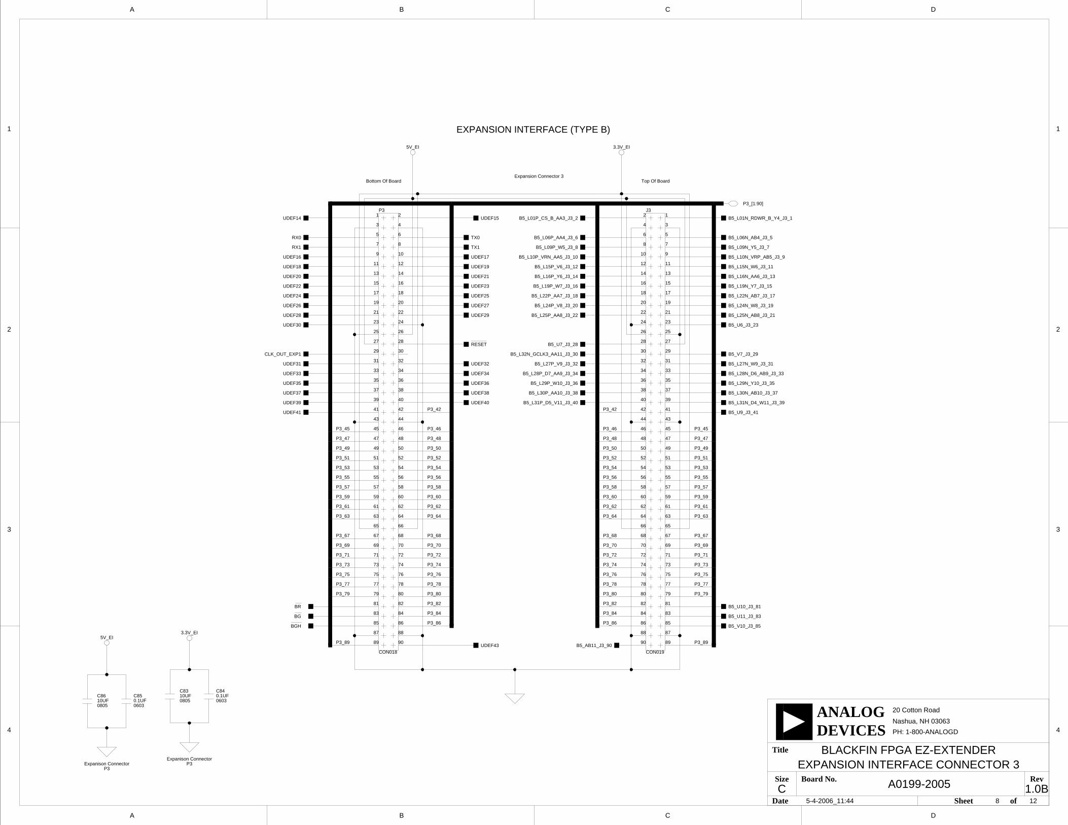
D
4
3
2
1
A B C
20 Cotton Road
Nashua, NH 03063
A B C D
4
3
2
1
PH: 1-800-ANALOGD
C
Title
Size Board No.
Date Sheet of
DEVICESANALOG
Rev
BLACKFIN FPGA EZ-EXTENDER
A0199-2005 1.0B
Expanison ConnectorExpanison Connector
Bottom Of Board Top Of BoardExpansion Connector 3
P3P3
EXPANSION INTERFACE (TYPE B)
5-4-2006_11:44 128
1
10
11 12
13 14
15 16
17 18
19
2
20
21 22
23 24
25 26
27 28
29
3
30
31 32
33 34
35 36
37 38
39
4
40
41 42
43 44
45 46
47 48
49
5
50
51 52
53 54
55 56
57 58
59
6
60
61 62
63 64
65 66
67 68
69
7
70
71 72
73 74
75 76
77 78
79
8
80
81 82
83 84
85 86
87 88
89
9
90
P3
CON018
1
10
1112
1314
1516
1718
19
2
20
2122
2324
2526
2728
29
3
30
3132
3334
3536
3738
39
4
40
4142
4344
4546
4748
49
5
50
5152
5354
5556
5758
59
6
60
6162
6364
6566
6768
69
7
70
7172
7374
7576
7778
79
8
80
8182
8384
8586
8788
89
9
90
J3
CON019
EXPANSION INTERFACE CONNECTOR 3
3.3V_EI5V_EI
TX0
TX1
UDEF17
UDEF19
UDEF21
UDEF23
UDEF25
UDEF29
UDEF27
RESET
UDEF32
UDEF34
UDEF36
UDEF38
UDEF40
B5_L01N_RDWR_B_Y4_J3_1
P3_42
P3_[1:90]
P3_86
P3_84
P3_82
P3_80
P3_78
P3_76
P3_74
P3_72
P3_70
P3_68
P3_64
P3_62
P3_60
P3_58
P3_56
P3_54
P3_52
P3_50
P3_48
P3_46
P3_42
P3_79
P3_89
P3_77
P3_75
P3_73
P3_71
P3_69
P3_67
P3_63
P3_61
P3_59
P3_57
P3_55
P3_53
P3_51
P3_49
P3_47
P3_45
P3_51
P3_79
P3_89
P3_77
P3_75
P3_73
P3_71
P3_69
P3_67
P3_63
P3_61
P3_59
P3_57
P3_55
P3_53
P3_49
P3_47
P3_45
P3_86
P3_84
P3_82
P3_80
P3_78
P3_76
P3_74
P3_72
P3_70
P3_68
P3_64
P3_62
P3_60
P3_58
P3_56
P3_54
P3_52
P3_50
P3_48
P3_46
B5_L27N_W9_J3_31
B5_L28N_D6_AB9_J3_33
B5_L29N_Y10_J3_35
B5_L30N_AB10_J3_37
B5_L31N_D4_W11_J3_39
B5_L10N_VRP_AB5_J3_9
B5_L25N_AB8_J3_21
B5_L24N_W8_J3_19
B5_L22N_AB7_J3_17
B5_L19N_Y7_J3_15
B5_L16N_AA6_J3_13
B5_L15N_W6_J3_11
B5_L09N_Y5_J3_7
B5_L06N_AB4_J3_5
B5_U6_J3_23
B5_V7_J3_29
B5_U9_J3_41
B5_L31P_D5_V11_J3_40
B5_L30P_AA10_J3_38
B5_L29P_W10_J3_36
B5_L28P_D7_AA9_J3_34
B5_L27P_V9_J3_32
B5_L32N_GCLK3_AA11_J3_30
B5_U7_J3_28
B5_L25P_AA8_J3_22
B5_L24P_V8_J3_20
B5_L22P_AA7_J3_18
B5_L19P_W7_J3_16
B5_L16P_Y6_J3_14
B5_L15P_V6_J3_12
B5_L10P_VRN_AA5_J3_10
B5_L09P_W5_J3_8
B5_L06P_AA4_J3_6
B5_L01P_CS_B_AA3_J3_2
B5_AB11_J3_90
B5_U11_J3_83
B5_V10_J3_85
B5_U10_J3_81
UDEF43
BGH
BG
BR
UDEF30
UDEF28
UDEF26
UDEF24
UDEF22
UDEF20
UDEF18
UDEF16
RX1
RX0
UDEF14 UDEF15
CLK_OUT_EXP1
UDEF31
UDEF33
UDEF35
UDEF37
UDEF39
UDEF41
3.3V_EI
C84
06030.1UF
080510UFC83
C8610UF0805
0.1UF0603
C85
5V_EI
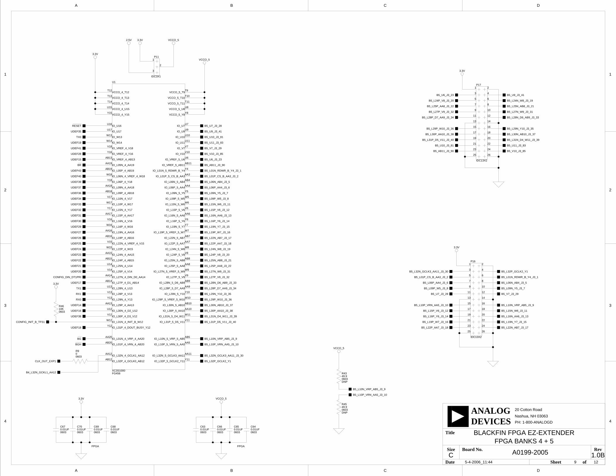
3.3V
3.3V
2.5V 3.3V
3.3V
3.3V
3.3V
D
4
3
2
1
A B C
20 Cotton Road
Nashua, NH 03063
A B C D
4
3
2
1
PH: 1-800-ANALOGD
C
Title
Size Board No.
Date Sheet of
DEVICESANALOG
Rev
BLACKFIN FPGA EZ-EXTENDER
A0199-2005 1.0B
VCCO_4_T12
VCCO_4_T13
VCCO_4_T14
VCCO_4_U15
VCCO_4_Y15
IO_U16
IO_U17
IO_W13
IO_W14
IO_VREF_4_V18
IO_VREF_4_Y16
IO_VREF_4_AB13
IO_L05N_4_AA19
IO_L05P_4_AB19
IO_L06N_4_VREF_4_W18
IO_L06P_4_Y18
IO_L09N_4_AA18
IO_L09P_4_AB18
IO_L10N_4_V17
IO_L10P_4_W17
IO_L15N_4_Y17
IO_L15P_4_AA17
IO_L16N_4_V16
IO_L16P_4_W16
IO_L19N_4_AA16
IO_L19P_4_AB16
IO_L22N_4_VREF_4_V15
IO_L22P_4_W15
IO_L24N_4_AA15
IO_L24P_4_AB15
IO_L25N_4_U14
IO_L25P_4_V14
IO_L27N_4_DIN_D0_AA14
IO_L27P_4_D1_AB14
IO_L28N_4_U13
IO_L28P_4_V13
IO_L29N_4_Y13
IO_L29P_4_AA13
IO_L30N_4_D2_U12
IO_L30P_4_D3_V12
IO_L31N_4_INIT_B_W12
IO_L31P_4_DOUT_BUSY_Y12
IO_L01N_4_VRP_4_AA20
IO_L01P_4_VRN_4_AB20
IO_L32N_4_GCLK1_AA12
IO_L32P_4_GCLK0_AB12
VCCO_5_T9
VCCO_5_T10
VCCO_5_T11
VCCO_5_U8
VCCO_5_Y8
IO_U7
IO_U9
IO_U10
IO_U11
IO_V7
IO_V10
IO_VREF_5_U6
IO_VREF_5_AB11
IO_L01N_5_RDWR_B_Y4
IO_L01P_5_CS_B_AA3
IO_L06N_5_AB4
IO_L06P_5_AA4
IO_L09N_5_Y5
IO_L09P_5_W5
IO_L15N_5_W6
IO_L15P_5_V6
IO_L16N_5_AA6
IO_L16P_5_Y6
IO_L19N_5_Y7
IO_L19P_5_VREF_5_W7
IO_L22N_5_AB7
IO_L22P_5_AA7
IO_L24N_5_W8
IO_L24P_5_V8
IO_L25N_5_AB8
IO_L25P_5_AA8
IO_L27N_5_VREF_5_W9
IO_L27P_5_V9
IO_L28N_5_D6_AB9
IO_L28P_5_D7_AA9
IO_L29N_5_Y10
IO_L29P_5_VREF_5_W10
IO_L30N_5_AB10
IO_L30P_5_AA10
IO_L31N_5_D4_W11
IO_L31P_5_D5_V11
IO_L32N_5_GCLK3_AA11
IO_L32P_5_GCLK2_Y11
IO_L10N_5_VRP_5_AB5
IO_L10P_5_VRN_5_AA5
FPGAFPGA
5-4-2006_11:44 9 12
49.90603
R45
DNP
R43
060349.9
DNP
T12
T13
T14
U15
Y15
U16
U17
W13
W14
V18
Y16
AB13
AA19
AB19
W18
Y18
AA18
AB18
V17
W17
Y17
AA17
V16
W16
AA16
AB16
V15
W15
AA15
AB15
U14
V14
AA14
AB14
U13
V13
Y13
AA13
U12
V12
W12
Y12
AA20
AB20
AA12
AB12
T9
T10
T11
U8
Y8
U7
U9
U10
U11
V7
V10
U6
AB11
Y4
AA3
AB4
AA4
Y5
W5
W6
V6
AA6
Y6
Y7
W7
AB7
AA7
W8
V8
AB8
AA8
W9
V9
AB9
AA9
Y10
W10
AB10
AA10
W11
V11
AA11
Y11
AB5
AA5
U1
FG456XC3S1000
7
2
4
8
10
6
3
9
11
13
15
17
19
21
23
25
12
14
16
24
26
22
20
18
1
5
P16
IDC13X2
5
1
18
20
22
26
24
16
14
12
25
23
21
19
17
15
13
11
9
3
6
10
8
4
2
7
P17
IDC13X2
R46
060310K
FPGA BANKS 4 + 5
VCCO_5
CONFIG_INIT_B_TFS1
CLK_OUT_EXP1
B4_L32N_GCKL1_AA12
R9
06030
B5_L10N_VRP_AB5_J3_9
B5_L10P_VRN_AA5_J3_10
VCCO_5
B5_L32P_GCLK2_Y1
B5_L32N_GCLK3_AA11_J3_30
CONFIG_DIN_DT1PRI
UDEF16
UDEF38
UDEF14
RX0
TX0
RX1
TX1
UDEF20
UDEF21
UDEF23
UDEF17
UDEF25
UDEF24
UDEF22
RESET
UDEF30
UDEF29
UDEF27
UDEF26
UDEF35
UDEF34
UDEF33
UDEF32
UDEF31
UDEF15
UDEF28
UDEF41
UDEF40
UDEF39
UDEF37
UDEF36
BR
UDEF43
BG
BGH
UDEF19
B5_L31P_D5_V11_J3_40
B5_L31N_D4_W11_J3_39
B5_L30P_AA10_J3_38
B5_L30N_AB10_J3_37
B5_L29P_W10_J3_36
B5_L29N_Y10_J3_35
B5_L28P_D7_AA9_J3_34
B5_L28N_D6_AB9_J3_33
B5_L27P_V9_J3_32
B5_L27N_W9_J3_31
B5_L25P_AA8_J3_22
B5_L25N_AB8_J3_21
B5_L24P_V8_J3_20
B5_L24N_W8_J3_19
B5_L22P_AA7_J3_18
B5_L22N_AB7_J3_17
B5_L19P_W7_J3_16
B5_L19N_Y7_J3_15
B5_L16P_Y6_J3_14
B5_L16N_AA6_J3_13
B5_L15P_V6_J3_12
B5_L15N_W6_J3_11
B5_L09P_W5_J3_8
B5_L09N_Y5_J3_7
B5_L06P_AA4_J3_6
B5_L06N_AB4_J3_5
B5_L01P_CS_B_AA3_J3_2
B5_L01N_RDWR_B_Y4_J3_1
B5_AB11_J3_90
B5_U6_J3_23
B5_V10_J3_85
B5_V7_J3_29
B5_U11_J3_83
B5_U10_J3_81
B5_U9_J3_41
B5_U7_J3_28
UDEF18
3
2
1
IDC3X1
P11
B5_L29N_Y10_J3_35
B5_L30N_AB10_J3_37
B5_L31N_D4_W11_J3_39
B5_U11_J3_83
B5_V10_J3_85B5_AB11_J3_90
B5_U10_J3_81
B5_L31P_D5_V11_J3_40
B5_L30P_AA10_J3_38
B5_L29P_W10_J3_36
B5_L28P_D7_AA9_J3_34
B5_L27P_V9_J3_32
B5_L28N_D6_AB9_J3_33
B5_L27N_W9_J3_31
B5_L25N_AB8_J3_21B5_L25P_AA8_J3_22
B5_L24N_W8_J3_19B5_L24P_V8_J3_20
B5_U9_J3_41B5_U6_J3_23
VCCO_5
C70
06030.01UF 0.01UF
0603
C69 C68
06030.01UF0.01UF
0603
C670.01UF0603
C66 C65
06030.01UF 0.01UF
0603
C64C63
06030.01UF
B5_L09N_Y5_J3_7
B5_U7_J3_28 B5_V7_J3_29
B5_L10P_VRN_AA5_J3_10 B5_L10N_VRP_AB5_J3_9
B5_L15P_V6_J3_12 B5_L15N_W6_J3_11
B5_L16P_Y6_J3_14 B5_L16N_AA6_J3_13
B5_L19P_W7_J3_16 B5_L19N_Y7_J3_15
B5_L22P_AA7_J3_18 B5_L22N_AB7_J3_17
B5_L32N_GCLK3_AA11_J3_30 B5_L32P_GCLK2_Y1
B5_L01P_CS_B_AA3_J3_2 B5_L01N_RDWR_B_Y4_J3_1
B5_L06P_AA4_J3_6 B5_L06N_AB4_J3_5
B5_L09P_W5_J3_8
VCCO_5B5_L10P_VRN_AA5_J3_10
B5_L10N_VRP_AB5_J3_9
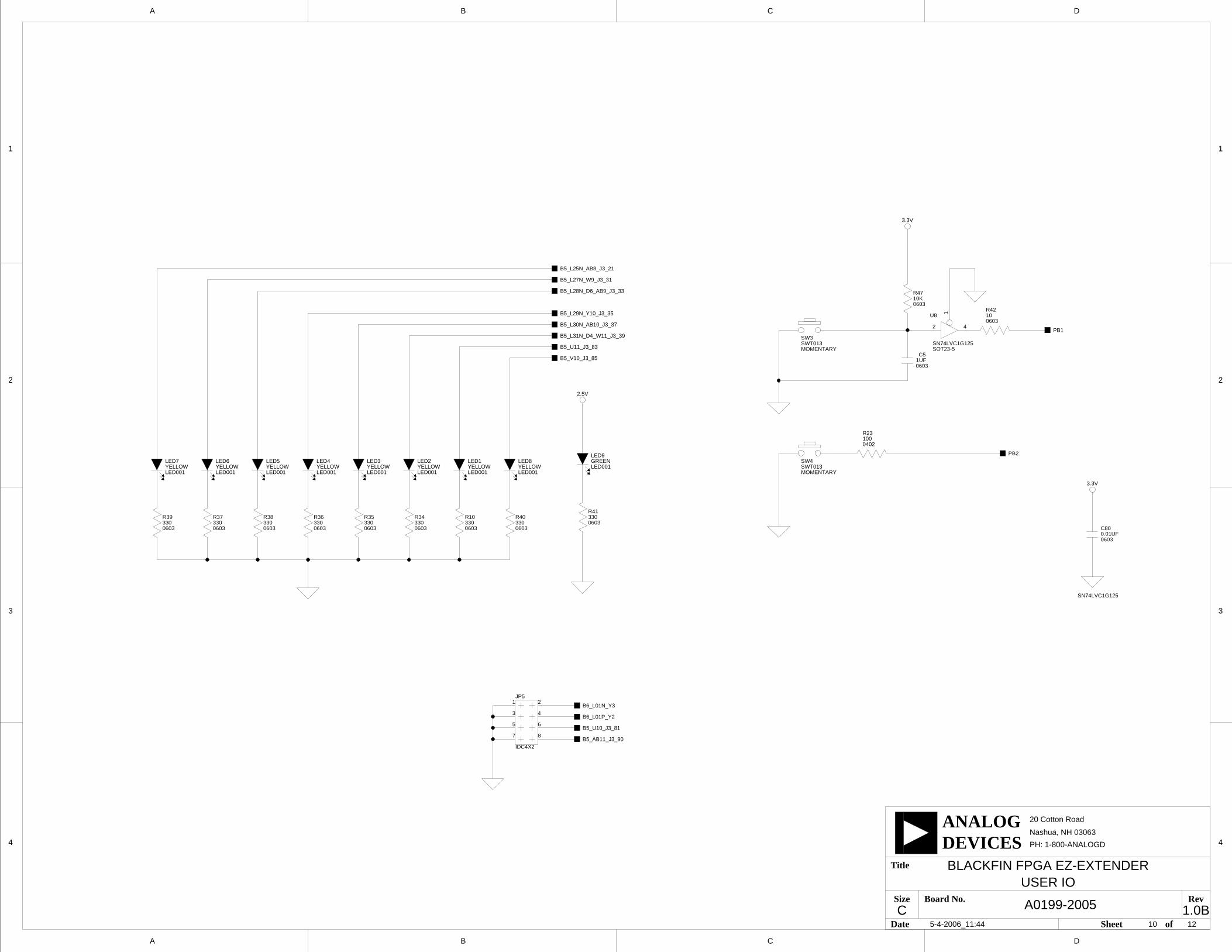
2.5V
3.3V
3.3V
D
4
3
2
1
A B C
20 Cotton Road
Nashua, NH 03063
A B C D
4
3
2
1
PH: 1-800-ANALOGD
C
Title
Size Board No.
Date Sheet of
DEVICESANALOG
Rev
BLACKFIN FPGA EZ-EXTENDER
A0199-2005 1.0B
SN74LVC1G125
5-4-2006_11:44 10 12
2 4
1
SOT23-5
U8
SN74LVC1G125
USER IO
C80
06030.01UF
SW4SWT013MOMENTARY
MOMENTARYSWT013SW3
060310R42
C5
06031UF
R413300603
LED001YELLOWLED8
0603330R40
LED7YELLOWLED001
R393300603
R1033006030603
330R34R35
33006030603
330R36
0603330R37 R38
3300603
LED001YELLOWLED2
YELLOWLED001
LED3YELLOWLED001
LED4YELLOWLED001
LED5
LED001YELLOWLED6
LED9GREENLED001
0402100R23
1 2
3 4
5 6
7 8
JP5
IDC4X2
YELLOWLED001
LED1PB2
B5_V10_J3_85
B5_U11_J3_83
B5_L31N_D4_W11_J3_39
B5_L30N_AB10_J3_37
B5_L29N_Y10_J3_35
B5_L28N_D6_AB9_J3_33
B5_L27N_W9_J3_31
PB1
B5_L25N_AB8_J3_21
R47
060310K
B5_AB11_J3_90
B5_U10_J3_81
B6_L01P_Y2
B6_L01N_Y3
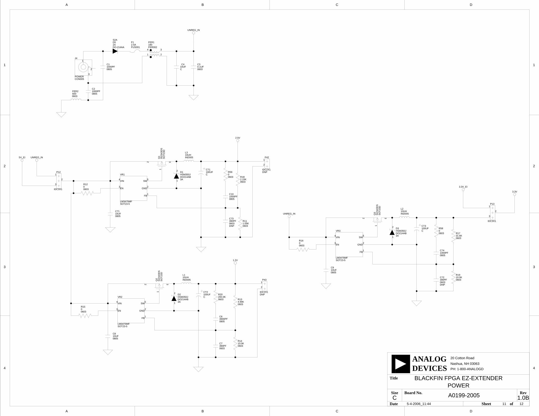
D
4
3
2
1
A B C
20 Cotton Road
Nashua, NH 03063
A B C D
4
3
2
1
PH: 1-800-ANALOGD
C
Title
Size Board No.
Date Sheet of
DEVICESANALOG
Rev
BLACKFIN FPGA EZ-EXTENDER
A0199-2005 1.0B
2.5V
3.3V
VIN
EN
SW
GND
FB
VIN
EN
SW
GND
FB
VIN
EN
SW
GND
FB
12115-4-2006_11:44
1
32
Q2
SO
T23
DS
I234
3DS
1
2
5
3
4
VR2
SOT23-5LM3475MF
4
3
5
2
1
VR1
SOT23-5LM3475MF
1
32
Q3
SO
T23
DS
I234
3DS
080510UFC9
C810UF0805
080510UFC71
4
3
5
2
1
VR3
SOT23-5LM3475MF
390PFC73
0603DNP 0603
R111.05K
0603
C72390PF
DNP
2 3
1Q
1
SO
T23
DS
I234
3DS
DO-214AA2AD5S2A
1
2
IDC2X1
P43
DNP
2
1P42
IDC2X1DNP
31.6KR17
0603
2.15KR18
0603
0805
C741000PF
0R58
0603
1000PFC10
0805
0603
R1910.0K
C100UFCT2
CT3100UFC
IND005
L110UH
10UHL3
IND005
10UHL2
IND005
1
2 D3
DO214AB3A
HSM350J
0603
R20200.0K
0805
C63900PF
390PFC7
0603
2
1 3ADO214AB
D2HSM350J
4.99KR13
0603
1
2 D1
DO214AB3A
HSM350J
3.3V_EI
3
1
2
IDC3X1
P13
UNREG_IN
1.2V
CT1100UFC
R1200603
5V_EI
08051000PFC2
FER2
0603600
06030.1UFC3
POWER
FUS0012.5AF1
4
1
3
2
FER002
FER1190
08051000PFC1
3
1
2
IDC3X1
P12
UNREG_IN
1
2
3
CON005POWER
J4
06030R15
R1600603
UNREG_IN
0603
R1410.0K
0603
R590
C410UFC
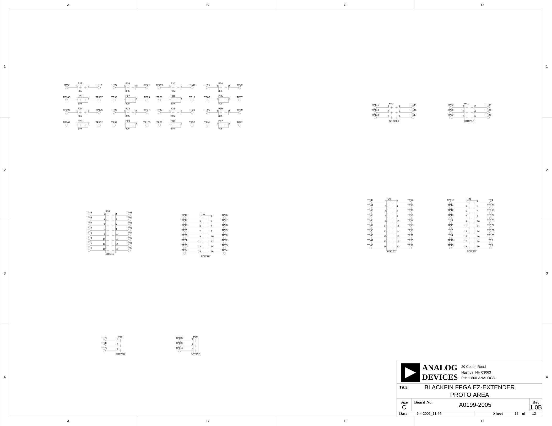
D
4
3
2
1
A B C
20 Cotton Road
Nashua, NH 03063
A B C D
4
3
2
1
PH: 1-800-ANALOGD
C
Title
Size Board No.
Date Sheet of
DEVICESANALOG
Rev
BLACKFIN FPGA EZ-EXTENDER
A0199-2005 1.0B12125-4-2006_11:44
1
3
65
4
2
SOT23-6
P402
4
5 6
3
1
SOT23-6
P41
5
2
4
8
10
6
1
3
9
11
13
15
17
19
12
14
16
20
18
7
P20
SOIC20
PROTO AREA
1
3
2
SOT23D
P39
2
3
1
SOT23D
P38
11
13
15 16
14
12
2
4
6
8
109
7
5
3
1
SOIC16
P191
3
5
7
9 10
8
6
4
2
12
14
1615
13
11
SOIC16
P18
21P37
805
1 2
805
P36
21P35
805
1 2
805
P34
1 2
805
P33
21P32
805
1 2
805
P31
21P30
805
1 2
805
P29
21P28
805
1 2
805
P27
21P26
805
21P25
805
1 2
805
P24
21P23
805
1 2
805
P22
TP86
TP85
TP84
TP83
TP82
TP81
TP80
TP79 TP77
TP76
TP75
TP74
TP73
TP72
TP71
TP70
TP68
TP67
TP66
TP65
TP64
TP62
TP61
TP60
TP59
TP58
TP57
TP56
TP55
TP54
TP53
TP51
TP50
TP49
TP48
TP47
TP46
TP45
TP44
TP43
TP41
TP40
TP39
TP38
TP37
TP36
TP35
TP34
TP33
TP32
TP30
TP29
TP28
TP27
TP26
TP25
TP24
TP23
TP22
TP21
TP19
TP18
TP17
TP16
TP15
TP14
TP13
TP12
TP11
TP9
TP8
TP7
TP6
TP5
TP4
TP125
TP124
TP123
TP122
TP121
TP120
TP119
TP118
TP117
TP116
TP114
TP113
TP112
TP111
TP110
TP109
TP108
TP107TP106
TP105TP103
TP102TP101 TP100TP99
TP98 TP97
TP96 TP95
TP94TP93
TP92TP91
TP90 TP89
TP88 TP87
TP78TP69
TP63 TP52
TP42 TP31
TP20 TP10
TP115TP104
7
18
20
16
14
12
19
17
15
13
11
9
3
1
6
10
8
4
2
5
SOIC20
P21
Blackfin FPGA EZ-Extender Manual I-1
I INDEX
Numerics2.5V header (P42), 2-17
AADSP-BF533/37/61 EZ-KIT Lite
interface, x, 1-3, 2-2ADSP-BF533/37/61 processors, boot
mode settings, 2-14architecture, of this EZ-Extender, 2-2asynchronous static random access memory
(SRAM), xauxiliary oscillator, xi, 1-4
Bbill of materials, A-1block diagram, of this EZ-Extender, 2-2board schematic, B-1boot jumper, See JP4
Cconfiguration jumpers, See JP2, JP3
connectorsmap of locations, 2-17J1-3 (expansion), 2-19P1-3 (expansion), 2-18P14 (IDC), 2-19P15 (JTAG header), 2-4P16-17 (IDC), 2-19P4 (high-speed), 2-20P5 (IDC), 2-20P6 (JTAG), 2-7P7 (IDC), 2-20P8 (IDC), 2-19
Ddone LED (LED10), 2-17
Eexpansion interface
connectors (P1-3, J1-3), 2-18of ADSP-BF533/37/61 EZ-KIT Lites, x,
1-3, 2-2external power supply, 1-3, 2-8
FField-Programmable Gate Array, See FPGAflash programming utility, 2-6
Index
I-2 Blackfin FPGA EZ-Extender Manual
FPGAdocumentation, 2-6input jumpers (JP5), 2-14software/firmware, 1-2Xilinx Spartan package, x, 1-3
FPGA pinsAB10 (LED3), 2-16AB11 (JP5.8), 2-14AB8 (LED7), 2-17AB9 (LED5), 2-17C11 (PB1/SW3), 2-16H5 (PB2/SW3), 2-16M2-0 (JP4), 2-13U10 (JP5.6), 2-14U11 (LED1), 2-16V10 (LED8), 2-17W11 (LED2), 2-16W9 (LED6), 2-17Y10 (LED4), 2-16Y3-2 (JP5.2-5.4), 2-14
FPGA programmingblock diagram, 2-3via ADSP-BF533/37/6 processors, 2-6via JTAG header, 2-4via serial ROM, 2-5
GGCLK1 (global clock 1) pin, 1-4GCLK6 (global clock 6) pin, 1-4general-purpose input push buttons, 2-16
Hhigh-speed connector (P4), 2-20
IIDC connectors, xi, 2-19, 2-20installation, of this EZ-Extender, 1-1
JJTAG
cable, 1-4, 2-7header (P6), 1-5, 2-4, 2-7, 2-14
jumpersmap of locations, 2-11JP1 (boot jumper), 2-5, 2-12JP2 (config done), 2-12JP3 (config program), 2-13JP4.1-4.6 (boot mode select), 2-5, 2-6,
2-13JP5.2-5.6 (FPGA input), 2-14
LLEDs
map of locations, 2-15LED10 (FPGA done pin), 2-4, 2-5, 2-17LED1-8 (status), 2-16LED9 (power), 2-17
MM2-0 (JP4) pins, 2-5master serial boot mode, 2-6MCS-86 Hexadecimal Object (.mcs) file
format, 2-6
Ooscillator, xi, 1-4
PP12 (power in) header, 2-9P13 (3.3V header), 2-9P42 (2.5V header), 2-10P43 (1.2V header), 2-10PB1 push button (SW3), 2-16PB2 push button (SW4), 2-16
Blackfin FPGA EZ-Extender Manual I-3
Index
PF14 flag pin (ADSP-BF537 EZ-KIT Lite), 2-12
PF3 flag pin (ADSP-BF533/61 EZ-KIT Lite), 2-12
power1.2V header (P43), 2-102.5V header (P42), 2-103.3V header (P13), 2-9in header (P12), 2-9LED (LED9), 2-17limitations, 2-8supplies, 1-3, 2-8
printed circuit board (PCB), 1-2product overview, xprogram push button (SW1), 2-4, 2-16push buttons
See also SWxmap of locations, 2-15
Sschematic, B-1serial ROM, 1-4
boot jumper (JP1), 2-12, 2-14programming via JTAG Header, 2-7
setup, of this EZ-Extender, 1-1
slave serial mode, 2-6SRAM memory banks, 1-4status reporting, 1-4, 2-16SW1 (program) push button, 2-4, 2-16SW3 (PB1) push button, 2-16SW4 (PB2) push button, 2-16switching regulators, 2-8
TTCK signal, 2-7TDI signal, 2-7TDO signal, 2-7technical support, xiiiTMS signal, 2-7
VVR1-3 regulators, 2-8
XXilinx
JTAG cable/software, 1-4, 2-4, 2-7JTAG header, 2-12serial ROM, 1-4