Embed Size (px)
Citation preview
. . . - - . 4
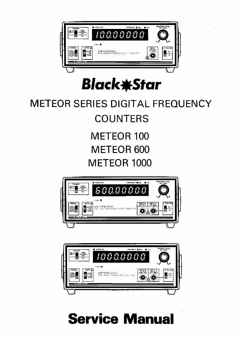
METEOtr ]OOSHz IOO MHz FaEGUENCY (:OlNTEtr
BIock*SforMETEOR SERIES DIGITAL FREOUENCY
COUNTERS
METEOR 1OOMETEOR 600
METEOR 1OOO
@ ffi !fl:r"="oJ--,g,?.GUE Ncy colNrEtr
ffi€l
.^-",.
METEOtr IOOO5H7-rCHz FFEOUENCY -O!NTEtr
Service Manual
METEOR SERIES FREOUENCY COUNTERSSERVICE MANUAL
INDEX
INTRODUCTlON
SPECIFICATION
FUNCTIONAL DESCRI PTION
CIRCUIT DESCRIPTION
CALIB RATION
TROUBLESHOOTING GUIDE
PARTS LIST
DIAGRAMS:
4
5
8
o
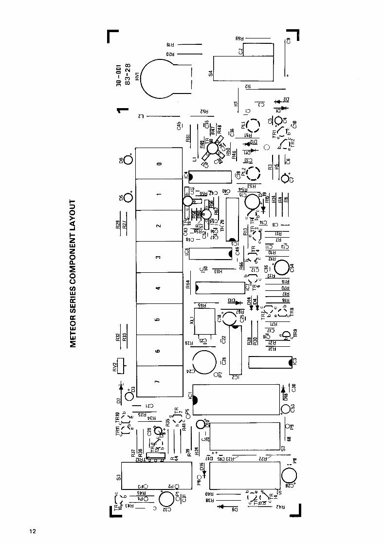
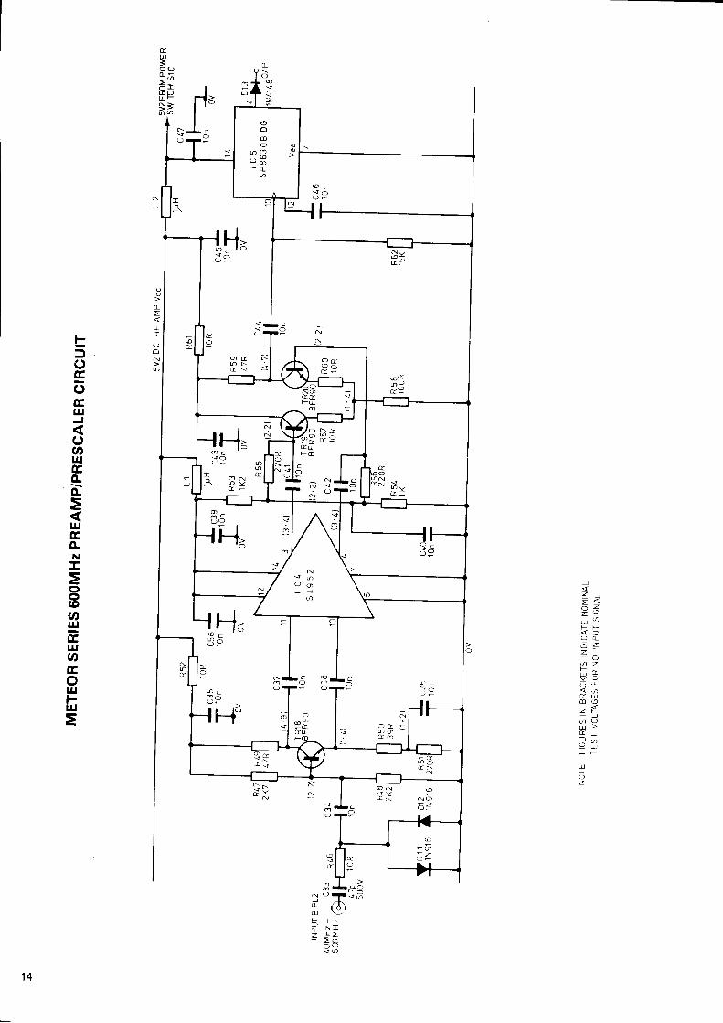
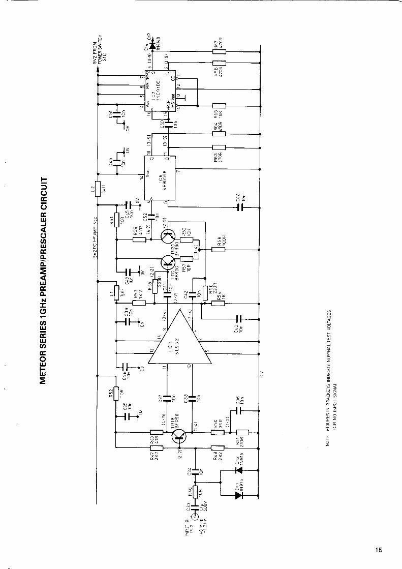
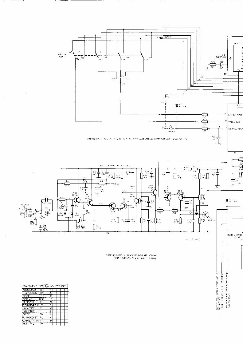
FUNCTIONAL BLOCK DIAGRAM 4COMPONENT LAYOUT 12MAlNS AND BATTERY CONNECTIONS 13600MHzPREAMP/PRESCALER CIRCUIT 141 GHz PREAMP/PRESCALER CIRCUIT 1sMAIN CIRCUIT 17
1. INTRODUCTION
al Handl ing
While the Meteor Counters have been designed to berugged, severe shocks can be destructive and shouldbe avoided. Suitable precautions against staticshould be taken as the unit contains CMOS compo-nents. Do not expose to radiant heat, including directsunlight for prolonged periods, or high humidity inc-luding conditions conducive to the formation of ice.Remove batteries if storing for prolonged periods. lfaccidentally immersed, rinse in fresh water, dry as faras possible after removing batteries, then stand in adry warm atmosphere (40oC - 60oC) away from dir-ect heat unti l dried.
bl Equipment
To check a Meteor 100 Frequency Counter, SignalGenerators must be available covering the band 2Hzto 100MHz. In addi t ion. generators cover ing theband 100MHz to 600MHz or lGHz (as appropr iate)are required to check Meteor 600 and 1000 models.The output level of all generators must be adjustableby a calibrated control. lt is helpful (though not ess-ential) if the output impedance is 50 Q .
Frequency calibration requires a highly stable signalsource of better than 1 x 10⁻⁷ error. ldeally an Off-AirFrequency Standard should be used. In the U.K. aBurns Frequency Standard SD-12 locked toDroitwich transmissions would be appropriate.
For routine servicing a 20MHz bandwidth Oscil lo-scope, preferably dual beam, with a sensitivity of5mV must be available, equipped with x10, 10MAinput impedance probes. An accurate Multimeter,preferably digital, capable of measuring 20V and500mA must be available.
The fo l lowing sundry equipment may a lso beneeded:-
Screwdriver - pozidrive No. 2 point.Soldering iron I solder.Desoldering tool (desolder wick may damage p.c.b.).Insulated trimming tool (or suitable insulated screw-dr iver) .Small hand tools (pliers, cutters etc. )Black Star Mains Adaptor or appropriate benchpower supply (9V 600mA).Set of 6 Nickel Cadmium cells, 'C' size, with a cap-acity of 1.2Ah or greater.Through termination ( 50 Q or as appropriate forsignal generator).Appropriate BNC connecting leads (at least one withcrocodi le c l ips l .
c) Dismantling
i l i Remove inst rument f rom packing.
i i) Remove knob from front panel by pull ingfrom shaft. lf i t is necessary to apply leverage,be careful not to apply side thrust to the po-tentiometer spindle.
i i i) Remove cells if fitted,
iv) Flemove metal leg by pushing inwards on oneside.
v) Unscrew the four recessed pozidrive screwsset into the feet on the underside of the case.
vi) Gently separate the two case halves.
vii) Remove front panel assembly and desolderBNC sockets and braid (if necessary). Whenoptional External Reference Oscillator facilityis f itted the 2 P . C. B . screws must be removed .
Disassembly is now complete. Reassembly is the re-verse of disassembly.
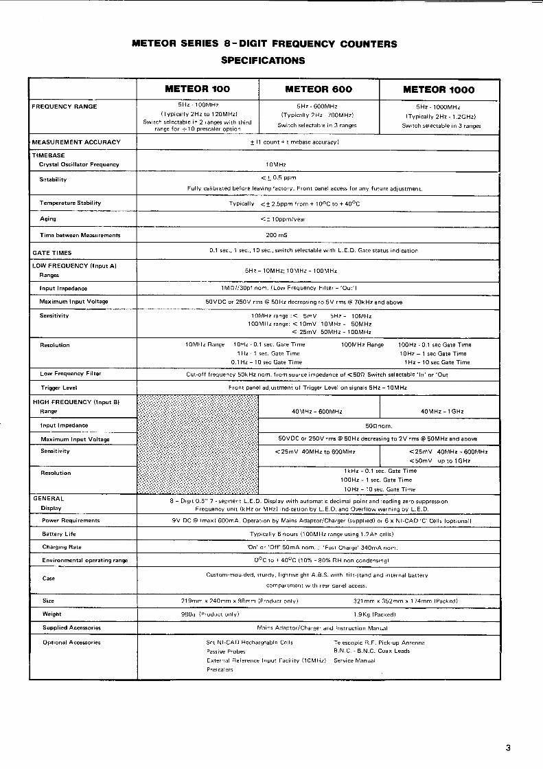
TETEOR SERIES 8-DIGIT FREQUENCY GOI'NTERS
SPECTFTCATtOilS
HETEOR lOO TETEOR 6()(, TETEOR IOOO
F R E O U E N C Y R A N G E 5 H z - 1 0 0 M H z
(Typ ica l l y 2Hz to 120MHz)Swi tch se lec tab le in 2 ranges w i th th i rd
range fo r =1O presca le r op t ion
sHz - 600MHz(Typical ly 2Hz - 700MHz)
Switch selectable in 3 ranges
SHz - 1 000MHz
(Typ ica l l y 2Hz - 1 .2GHzl
Switch selectable in 3 ranges
MEASUREMENT ACCURACY t (1 count + t imebase accuracy)
TIMEBASECrystal Oscillator Frequency l 0 M H z
Setabil i ty < i 0 .5 ppm
Ful ly ca l ib ra ted be fore leav ing fac to ry . Fron t pane l access fo r any fu tu re ad j us tment .
Temperature Stabil ity Typ ica l l y <12.5ppm f rom + 1OoC to + 4OoC
Aging < I 1 Oppm/year
Time between Measurements 200 mS
GATE TIMES 0.1 sec . , 1 sec . , 1 0 sec . , sw i tch se lec tab le w i th L .E .D. Gate s ta tus ind ica t ion
LOW FREOUENCY ( lnput A)
Ranges5 H z - 1 0 M H z ; 1 0 M H z - 1 0 0 M H z
Input I mpedance 1 M o / / 3 0 p f n o m . ( L o w F r e q u e n c y F i l t e r - ' O u t ' )
Maximum I nput Voltage 50VDC or 250V rms @ 50Hz decreas ing to 5V rms @ 70kHz and above
Sensitivity 1 o M H z r a n g e : < 5 m V s H z - 1 o M H z1 0 0 M H z r a n g e : < l 0 m V 1 0 i \ 4 H z - 5 0 N 4 H z
< 2 5 m V 5 0 M H z - 1 0 0 M H z
Resolution lo l \ i lHz Range 1 oHz - 0 .1 sec . Gate T ime
1 F lz ' 1 sec . Gate T ime
0 . 1 H 2 - 1 0 s e c G a t e T i m e
100MHz Range 100H2 - 0 .1 sec Gate T ime
1OHz - 1 sec Gate T ime
1 Hz - 10 sec Gate T ime
Low Frequency Filter Cut -o f f f requency 50kHz nom. f rom source impedance o f <50Q Swi tch se lec tab le ' ln 'o r 'Out
Trigger Level Fron t pane l ad jus tment o f T r igger Leve l on s igna ls 5Hz - 101\4Hz
H I G H F R E O U E N C Y ( l n p u t B )
Range iiii 40 lVHz - 600MHz 4 0 M H z - 1 G H z
I nput I mpedance 50Qnom.
Max imum Input Vo l tage 50VDC or 250V rms @ 50Hz decreas ing to 2V rms @ 50MHz and above
Sensitivity <25mV 40MHz to 600MHz <25rnv 40MHz - 600MHz<50mV up t o l GHz
Reso lu t ion ffi jrl kHz - 0 .1 sec . Gate T ime
100H2 - 1 sec . Gate T ime
1 0 H z - 1 0 s e c . G a t e T i m e
G E N E R A L
Display8 - D ig i t 0 .5" 7 - segment L .E .D. D isp lay w i th au tomat ic dec ima l po in t and lead ing zero suppress ion .
Frequency un i t (kHz or MHz) ind ica t ion by L .E .D. and Over f low warn ing by L .E .D.
Power Requirements 9V DC @ (max) 600mA. Opera t ion by Mains Adaptor /Charger (supp l ied) o r 6 x N l -CAD'C 'Ce l ls (op t iona l )
Battery Life Typ ica l l y 6 hours {100MHz range us ing ' l .2Ah ce l l s )
Charging Rate ' O n ' o r ' O f f ' 5 0 m A n o m . ; ' F a s t C h a r g e ' 3 4 O m A n o m .
Environmental operating range OoC to + 4OoC (10% - 80% RH non-condens ina)
GaseCustom-moulded, s ru rdv , l igh twe igh t A .B.S. w i th ta l r -s tand and in te rna l ba t te ry
c o m p a r t m e n t w i t h r e a r p a n e l a c c e s s
S ize 2 1 9 m m x 2 4 0 m m x 9 8 m m ( P r o d u c t o n l v ) 3 2 1 m m x 3 5 2 m m x 1 7 4 m m ( P a c k e d )
Weight 9809 (Produc t on ly ) 1 . 9 K 9 { P a c k e d )
Supplied Accesories Mains Adaptor /Charger and Ins t ruc t ion Manua l
Optional Accesories Set N l -CAD Rechargeab le Ce l ls
Passive Probes
Externa l Reference lnput Fac i l i t y ( ' l 0Ml - i z )
Prescalers
Te lescop ic R.F . P ick -up AntennaB.N.C. - B .N.C. Coax Leads
Serv ice Manua l
3
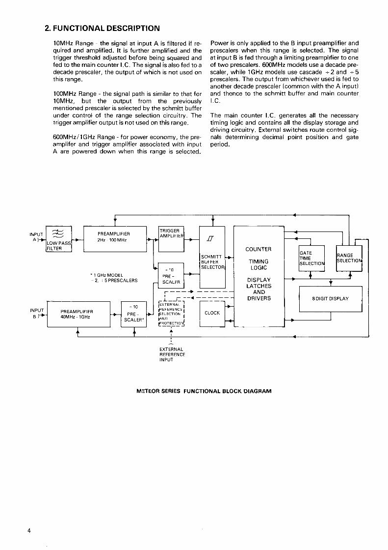
2. FU N CTIONAL DESCRIPTION
l0MHz Range - the signal at input A is f i l tered if re-quired and amplif ied. lt is further amplif ied and thetrigger threshold adjusted before being squared andfed to the main counter l .C. The s ignal is a lso fed to adecade prescaler, the output of which is not used onth is range.
100MHz Range - the s ignal path is s imi lar to that for' l0MHz, but the output from the previouslymentioned prescaler is selected by the schmitt bufferunder control of the range selection circuitry. Thetrigger amplif ier output is not used on this range.
600MHz/1GHz Range - for power economy, the pre-ampl i fer and t r igger ampl i f ier associated wi th inputA are powered down when this range is selected.
Power is only applied to the B input preamplif ier andprescalers when this range is selected. The signalat input B is fed through a l imiting preamplif ier to oneof two prescalers. 600MHz models use a decade pre-scaler , whi le lGHz models use cascade -2 and -+5prescalers. The output from whichever used is fed toanother decade prescaler (common with the A input)and thence to the schmitt buffer and main counterr .c .
The main counter l.C. generates all the necessarytirning logic and contains all the display storage anddriving circuitry. External switches route control sig-nals determining decimal point position and gateoeriod.
PREAMPL IF IER2Hz - 100 MHz
COUNTER
TIMINGLOGIC
DISPLAYLATCHES
ANDDRIVERS| - - - a
- ! - J - 1
lexrrnrunr I f------LI R E F E R E N C E i | ^ , ^ ^ , , I
8 DIGIT DISPLAY
PREAMPL IF IERz l O M H z ' l G H z
' ' l GHz MODEL=2 , +5 PRESCALERS
-lEXTERNALREFERENCEINPUT
METEOR SERIES FUNCTIONAI- BLOCK DIAGRAM
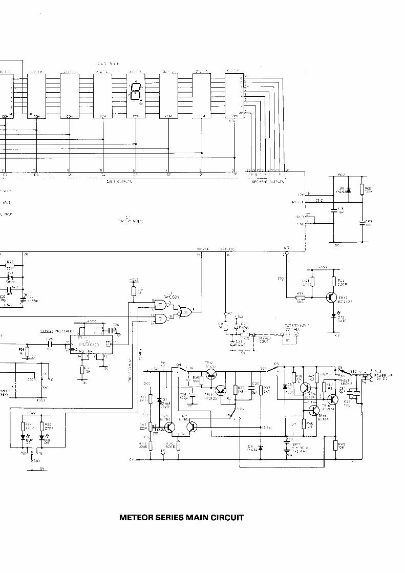
3. CIRCUIT DESCRIPTION
Power SupplyThe instrument operates from a stabilised supplywhich uses the band-gap diode D8 as a 2.45V refer-ence. D7 acts as an overvoltage capture diode whensett ing up the suppy with RV2. TR10 and TR11 forma long tailed pair differential amplifier feeding TR13and TR12 current ampl i f ier. When rechargeable cel lsare fitted, power is fed via D9. When a Mains Adap-tor is used, trickle charging of the battery takes placeby the constant current supply TR14, TR15 and asso-ciated components. D9 is reverse biased, overridingthe battery supply. In the fast charge conf igurat ion,TR12 and TR13 form the pass element for a constantcurrent source using R43 for current sensing and theVbe of TR 1 6 as a reference.
10MHz/100MHz Preampli f ier
Cl and C3, R1 and R2, D1 and D2form an input pro-tection and clamp network, capable of withstandingshort term connection to240Y a.c. at 50-60H2 (stressrating only). R69 and C2 form a switch selectable50KHz Low Pass Filter. TR1 and TR2 are emitterfollower buffer amplifiers, biased from the collectorof TR3, and bootstrapped from the emitter of TR2 togive very high input impedance. TR3 and TR4 form alongtailed pair voltage amplifier, the output beingtaken from the collector of TR4 to avoid collector-base feedback limiting bandwidth. TR5 defines theworking point, and D19 prevents TR3 from satura-t ing with high input levels. TR6 is an emit ter fol lowerbuffer and level shifter to ECL levels. From the emit-ter of TR6 the signal is fed to lC2, a ECL prescaler,and the base of TR7. TR7 and TR8 form a vol tageampli f ier, with TR9 as an output ampl i f ier/CMOSbuffer stage. Overall feedback is applied by R70 andR71 to def ine a gain of 30. The working point of TR8,and hence the tr igger level is set by RV1.
600M Hzl1 G Hz preamplifier
C33 provides isolation for accidental mains voltageinputs, and R46 in conjunction with D11 and D12pro-vide.s some protection at high frequencies. C34couples the signal to the base of TR18, a low-levelcurrent amplifier and phase-splitter. Antiphase sig-nals are coupled by C37 and C38 to lC4, a monolithicvoltage amplifier. The antiphase outputs are fed toTR19 and TR20, a longtailed pair providing furthervoltage amplification to a level adequate for ECLoperation. The output is fed to the appropriate pre-scaler by CM or C52.
Prescalers
The lGHz model has a lGHz -2ECL prescaler, lC6,fed from C52, which in turn feeds lC7, a 600MHz,- 5 ECL prescaler. The 600MHz model only uses oneprescaler for this function, lC5, a 600MHz * 1g 561device. These prescalers and preamplifiers have theirsupply switched on as required by the range switch51. D4, D13 and D14 determine which signal is fed tothe input of lC2, another 600MHz - 10ECL prescaler,but this time offering a TTL compatible output. Thisis adequate to drive lC3, a high-speed CMOS schmitttrigger quad nand gate. 51 also selects between10MHz inputs and any other range. With most sinu-
soidal inputs the output f rom lC3 is a 1 :1 mark-spaceratio square wave suitable for driving lC1. C25, at theinput to lc2, allows the internal biassing of lc2 tocorrect for the d.c. shi f t caused by D4, D13 or D14.
lMain counter lC1
a ) Input. The input on pin 28 is a CMOS struc-ture capable of accepting 1 :1 mark space ratioinputs up to typically 12MHz, allowing someoverrange capability.
b ) Range selection. The internally generateddecimal point is disabled bV D17 , and selectedexternally by the digit strobe routed to pin 13.As this is dependant on resolution, and hencegate t ime, S1B, S2B, S2C and S2D form acomplex switching net selecting the appro-priate digit. D15 prevents a latch-up conditionduring range selection.
c ) Gate time selection. This is carried out byS2A selecting the appropriate digit strobe todr ive pin 14.
d ) Reset. Occurs automatically on power-updue to the action of C53 and R68 on pin 12.D18 prevents damage (due to stored chargein C53) when the unit is switched off .
e ) Gate period. Pin 2 provides a measurement inprogress signalwhich is buffered and invertedby R39, R41, R44 and TR17 to dr ive D10 witha constant current.
f ) Dispfay Common cathode Digits 0 - 7 are dir-ectly driven by lC1, no limiting resistors beingnecessary. Matched high-efficiency displaysare used, so to get even intensity the intensitycode must be specified when ordering spares.
g) Indicators D3 replaces the decimal point ofDigit 7 to indicate overflow but due to its highsensitivity C21 and R25 are necessary to avoidghosting. D5 and D6 are not directly drivenfrom lC1 but are switch selected with lC3 in-puts to indicate the display scaie factor.
h) Osciffator XLl, R26, C22, C23 and C24 to-gether with a CMOS inverter between pin 25and 26 form a precision oscillator. R26 biasesthe inverter, while C22, C23 and C24 lcad andtune the crystal for 10MHz operation. Note,for stability, only cold welded crystal typesshould be used for replacement, not solderedcan.
i) External Reference Oscillator facility Pin24is an external oscillator input and when usedan input protection circuit is employed. FromPL4, C27 and R9 decouple d.c. and l imitsurge current to the protection diodes (D20,D21). These diodes prevent excursion morethan 0.8V beyond either rail. R8 limits inputcurrents to about lzmA under these
conditions, preventing destructive latch-up.D20 and D21 are a compromise betweensurge capacity and speed, and should not besubstituted for other types. The external osci-llator option is selected on lC1 by theinclusion of D16 and an appropriate switch.
i ) Main Counter l .C. Pins 1, 13 and 14 on themain counter l .C. are the control , decimalpoint and range inputs respectively. These areselected by strobing with one or more of thedisplay digi t dr ive signals (act ive LOW). Theeffect of various connections is shown below:
Control Display Effect/CommentsInput Digit
Counterl .C. pin 1 to: Do External osci l lator
input enabled
Dr Selects lMHz refer-ence clock opt ion.
D2 External decimal pointenable. Activatesp in 13 .
D3 Blank display whenhold input (pin 27) ish igh .
D4 Test mode, neverused. Counter latchesrandom display.
D7 Display test. All seg-ments lit. Overriddenby D3.
Decimal Display Effect/GommentsPoint DigitinputCounterl . C . o i n13 to: Do-Du Lights corresponding
decimal point(s).
RangeInputCounterl . C . p i n14 to :
D7 Lights over f low Le.d.Disables overflow andb lank ing .
Display Effect/CommentsDigit
Do Gate time 10 msselected
Dl Gate time 100 msselected
D2 Gate time 1 secselected
D3 Gate time 10 secselected
4. CALIBRATION
The Meteors are designed to require a minimum ofcalibration. Two adjustments only are required. Forthe first, Vcc, it is necessary to dismantle the case(but NOT the front panel) see Section 1c - Dis-mantling. When the case has been separated leavethe printed circuit board assembly in the case lower.Attach a meter (6VDC minimum) between test pinsP9 (lowest test point below gate time switch) -ground, and P8 (lowest test point below rangeswitch) - Vcc. The voltage measured should be5,2V t 0.05V. lf incorrect, adjust RV2, the trimmer atthe top of the front panel assembly, untilwithin lim-its. This adjustment is normally only needed if powersupply components have been changed.
The second adjustment, the crystal clock calibration,is required if crystal drift exceeds requirements. Nodismantling is required for this, but as the metaltrimmer is at vcc potential it is ESSENTIAL that aninsulated trimming tool is used. A Vcc short circuit toground (via the front panell will damage the powersupply and regulation circuitry.
Normally, a minimum 5 minute warm-up period is re-quired for the instrument to reach a stable operatingtemperature. Connect a frequency standard ofknown accuracy (0.1ppm or better) to input 'A'.
Typically a 1OMHz source would be used and the foll-owing description assumes this:
Set the front panel controls to filter out,power on, 10MHz range, 0.'l sec gate, andadjust trigger level to obtain a stable reading.Set to 10.00000 t 1 digit using the trimmingcapacitor accessible through the front panel.Select 1 sec gate and carefully trim for areading between 9.999995 and 10.000004.Typically an error of 0,2ppm can be achieved,but the temperature during calibration shouldbe noted for maximum accuracy.
5. TROUBLF SHOOTING AND FAULTLOCATION
It is worth checking all control settings before look-ing for a fault. Particular attention should be paid tothe External Reference Oscillator switch, if fitted, theTrigger Level Control (very sensitive at low levels,and/or high frequencies) and the Low-Pass Filterswitch.
Where no socket has been used for an integratedcircuit, this is an intended part of the design and notan economy measure. Stray capacitance willdegrade performance. To replace an unsocketedfaulty l.C. it is recommended (to minimise risk ofp.c.b. damage) that al l the legs on the l .C. becropped and removed individually.
Note that typical voltages are shown on the circuitdiagrams. These apply in the absence of input signaland switches selected as shown. lt is assumed thatthe 600MHzl1GHz range is selected when testingthese prescalers. The power supply voltages areindependant of control settings, and are appropriatewhen a mains adaptor is in use.
Power Supply A wide variety of unrelated faults canoccur if the wrong Vcc is present. lf in doubt aboutany fault, ALWAYS check that Vcc is within limits,and repair or recalibrate if necessary.
Prescalers and preamplifiers These do not nor-mally give trouble. lf signal is not being passed,check for presence of Vcc for the appropriate part ofthe circuitry, and confirm absence of evidence ofuser servicing (solder splashers, lifted or brokentracks etc.) before checking voltages round the cir-cuit. The H.F. preamplifier and prescalers will workwith reduced sensitivity with a l0MHz input signal,and allowing the use of a low cost osciiloscope forsignal tracing. A 10M4,10:1 attenuator probe shouldbe used for this.
Main Counter lf only one digit l ights up, but with ahigh intensity, suspect the crystal clock. Checkingthe frequency on pin 25 is quite likely to load theclock enough to stop oscillation. Pin 26 should givegood results with a high inrpedance probe.
The display digit strobes are used for control of somecounter l.C. functions. Serious leakage can occurand cause a variety of problems. The input thresh-olds on the main counter i.c. lie between 3.2 and4.4V so aggregate leakage over 4pA can give trouble,which may appear as a ghosting digit or an extradecimalpoint.
The tracks in the region of the display are very fine,and track damage or solder shorts can easily occur,Careful inspection may be necessary if faults remainafter servicing.
External Reference Oscillator Input There are fewthings that can go wrong here. The important pointis to ensure adequate drive is available for this or thedisplay will exhibit a bright digit zero as the maincounter l.C. selects the external oscillator input,waits 51rs (200KHz minimum input frequency), thenreverts to the internal clock. The remaining digits arecorrespondingly dimmer due to the increased cycletime. lf in doubt, check that the signal level is ade-quate at the main counter l.C. input (pin 24l. (CMOSlevels20% -80% of Vcc).
In general, note that excessively low input signals willgive a reading which jitters, or no reading at all. The600MHz and lGHz prescalers self oscillate in the ab-sence of an input, giving a false display typically inthe region 600-700MH2. This will not affect normalsensitivity, and actually enhances it near the(random) frequencies of oscillation. The self oscilla-tion does NOT give a stable display in the absence ofan input signal.
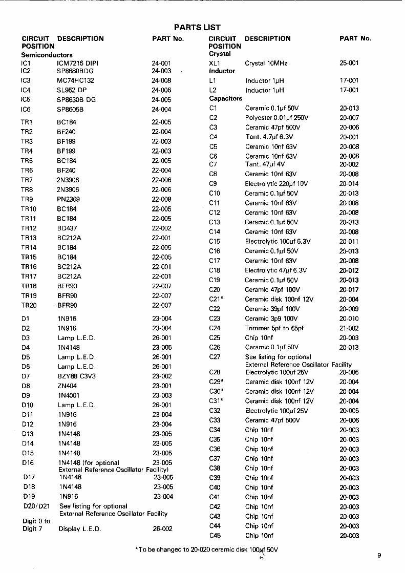
PARTS LISTCIRCUIT DESCRIPTIONPOS|TTONSemiconductors
PART No.
24-00124-00324-00824-00624-W524-004
22-00522-W422-00322-00322-40522-@422-00622-00622-00822-00522-00522-00222-00122-00522-00522-00122-00122-OO722-00722-007
23-00423-00426-00123-00526-00126-00123-00223-00123-00326-00123-W423-00423-00523-00523-00523-005
Facil ity)23-00523-00523-N4
L1L2Capacitorsc1c2c3c4c5c6c7c8c9c10c11c12c13c14c15c16c17c18c19c20c21*c22c23c24c25c26c27
c28c29*c30*c31*c32c33c34c35c36c37c38c39c40c41c42c43c4c45
PART No.
2$001
17-00117-001
20-01320-0o720-00620-00120-00820-00820-w220-00820-01420-01320-00820-00820-0132GOOB20-0112tF0132GOGtuo122G013n-0172G0042G00920-01021-n220-00320-013
Facility20-00520-00420-00420-m420-00520-0062G0032G00320-0032Gm32G0032G0032Gm32Gm32G0032G0032Gm32G003
CIRCUIT DESCRIPTIONPOStTtONGrystalXL1 Crystal 10MHzlnductor
tc1tc2rc3rc4rc5rc6T R 1TR2TR3TR4TR5TR6TR7TR8TR9T R l OT R 1 1T R 1 2T R 1 3T R 1 4T R 1 5T R 1 6T R 1 7T R 1 8T R 1 9TR20
D 1D2D3D4D5D6D7D8D9D 1 0D 1 1D12D 1 3D 1 4D 1 5D 1 6
tcM7216 DtPlSP868OBDGMC74HC13251952 DP
SP863OB DGSP86O5B
8C184BFz4o8F1998F199BC'r84BF24o2N39062N3906PN23698C1848C184BDIBTBC212ABC184BC184BC212ABC212ABFRgOBFRgOBFRgO
1 N 9 1 61 N 9 1 6Lamp L .E.D.1N4148Lamp L .E.D.Lamp L .E.D.BZY88 C3V32N4041 N4001Lamp L .E.D.1 N 9 1 61 N 9 1 61N41/E1N41481N41/E1N4148 (for optionalExternal Reference Oscillatot
Inductor 1pHlnductor 1pH
Ceramic 0.1uf 50VPolyester 0.01pf 250VCeramic 47pf 500VTant, 4.7uf 6.3VCeramic 1Onf 63VCeramic 10nf 63VTant.471tf 4V
Ceramic 10nf 63VElectrolytic 220pf 1AYCeramic 0.1rrf 50VCeramic 1Onf 63VCeramic 1Onf 63VCeramic 0.1trf 50VCeramic 1Onf 63VElectrolytic 1 00uf 6.3VCeramic 0.1uf 50VCeramic 1Onf 63VElectrolytic 47pf 6.3VCeramic 0.1uf 50VCeramic 47pf 100VCeramic disk 100nf 12VCeramic 39pf 100VCeramic 3p9 100VTrimmer Spf to 65pfChip 10nfCeramic 0.1pf 50V
See listing for optionalExternal Reference OscillatorElectrolytic 100pf 25VCeramic disk 100nf 12VCeramic disk 100nf 12VCeramic disk 100nf 12VElectrolytic 1001f 25VCeramic 47pf 500VChip 10nfChip 10nfChip 10nfChip 10nfChip 10nfChip 10nfChip 10nfChip 10nfChip 10nfChip 1OnfChip 10nfChip 10nf
D17 1N41rED18 1N4148D 1 9 1 N 9 1 6DzOlD21 See listing for optional
Digit 0 toDigi t 7 Display L.E.D.
External Reference Oscillator Facility
26-m,2
*To be changed to 20-020 ceramic disk 100p( 50Via'
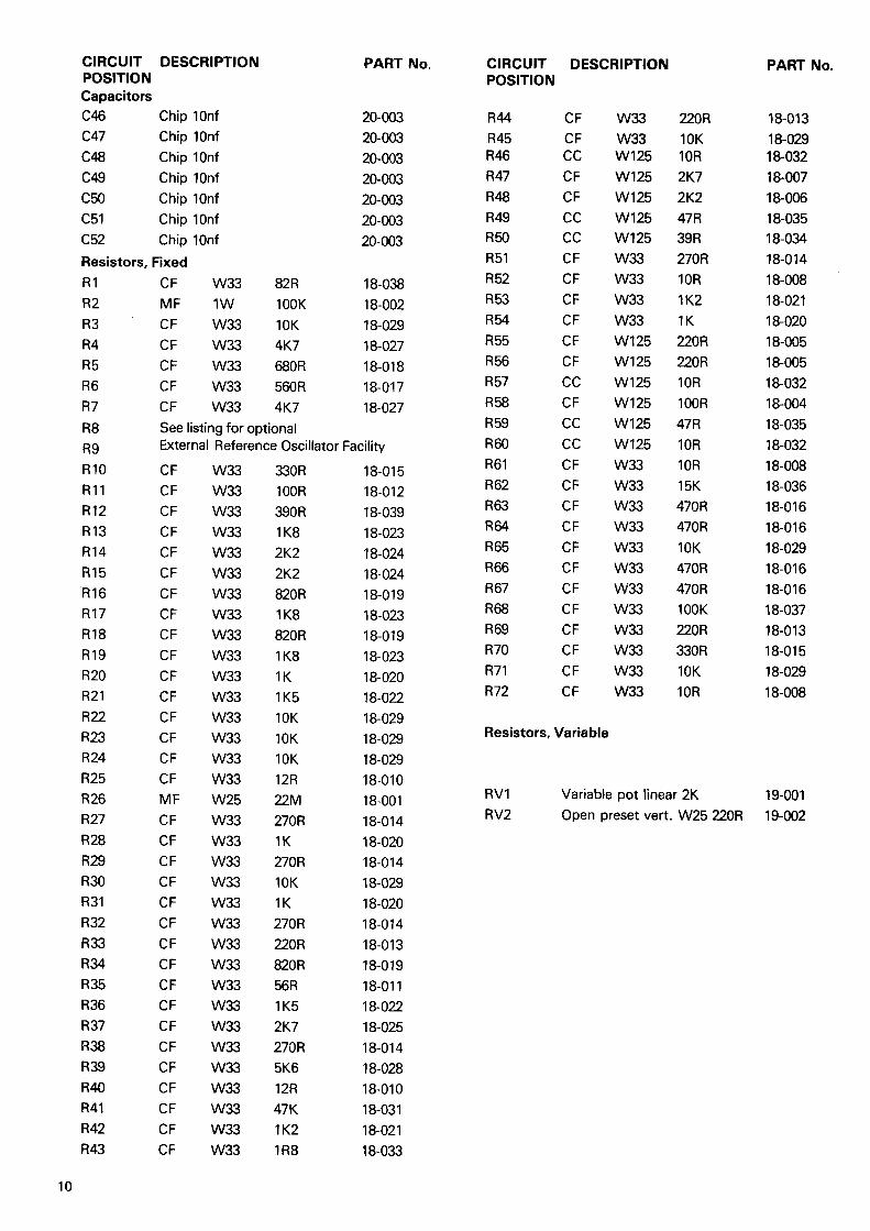
CIRCUIT DESCRIPTIONPOSITIONCapacitors
Resistors, FixedR 1R2R3R4R 5R6R7
R8R9R 1 0R 1 1R12R 1 3R 1 4R 1 5R 1 6R 1 7R 1 8R 1 9R20R21R22R23R24R25R26R27R28R29R30R31R32R33R34R35R36R37R38R39RlmR41R42R43
Chip 1OnfChip 10nfChip 1OnfChip 10nfChip 10nfChip 10nfChip 10nf
CF W33CF W33
PART No.
20-00320-00320-00320-00320-00320-00320-003
18-03818-00218-02918-02718-01818-01718-027
18-01518-01218-03918-02318-02418-02418-01918-02318-01918-02318-02018-02218-02918-02918-02918-01018-00118-01418-02018-01418-02918-02018-01418-01318-01918-01 118-02218-02518-01418-02818-01018-03118-02118-033
w33 220Rw33 10Kw125 10Rw125 2K7w125 2K2w125 47Rw125 39Rw33 270Rw33 10Rw33 1K2W33 lKw125 220Rw12s 220Rw125 10Rw125 100Rw125 47Rw125 10Rw33 10Rw33 15Kw33 470Rw33 470Rw33 10Kw33 470Rw33 470Rw33 100Kw33 220Rw33 330Rw33 10Kw33 10R
PART No.
18-01318-02918-03218-00718-00618-03518-03418-01418-00818-02118-02018-00518-00518-03218-00418-03518-03218-00818-03618-01618-01618-02918-01618-01618-03718-01318-01518-02918-008
CIRCUIT DESCRIPTIONPOSTTTON
c46c47CrACrtgc50c51c52
R44R45R46R47R€R49R50R51R52R53R54R55R56R57R58R59R60R61R62R63R64R65R66R67R68R69R70R71R72
CFCFccC FC FccccC FC FCFC FCFC FccC FccCCC FC FC FC FC FC FC FC FC FC FC FC F
cF w33 82RMF 1W 1OOKcF w33 10KcF w33 4K7cF w33 680RcF w33 560RcF w33 4K7See listing for optionalExternal Reference Oscillator Facility
cF w33 330RcF w33 100RcF w33 390RcF w33 1K8cF w33 2K2CF W33 2K2cF w33 820RcF w33 1K8cF w33 820RcF w33 1K8CF W33 1KcF w33 1K5cF w33 10KcF w33 10KcF w33 10KcF w33 12RMF W25 22McF w33 270RCF W33 1KCF W33 27ORcF w33 10KCF W33 1KcF w33 270RcF w33 220RcF w33 820RcF w33 56RcF w33 1K5cF w33 2K7cF w33 270RcF w33 5K6cF w33 12RcF w33 47K
Resistors, Variable
RV1RV2
Variable pot linear 2K 19-001Open preset vert. W25 220R 19-002
1K21R8
1 0
DESCR!PTIONP . C . B .Socket, Displays (80)*
Switch, 4P3W, sl ide (S1/S2lS3)
Switch, 2P2W, slide (54)
Socket l .C . 28 p in D. l .L .Socket, power input (PL3)
HeatsinkWasher, micaWasher, insulating (2)
Screw, 684 x 6mm Round Head**(for Heatsink)Washer. 684Nut 684Washer lock 684Socket, BNC with nut & washer(PL1IPL2I
Tag BNCPins, terminal ( P1 -P9)***
Front panel printed 100MHzFront panel printed 600MHzFront panel pr inted lGHz
Miscellaneous
Case upper with insertsCase lower drilledCase expansion strip (2)
Foot A (2)
Foot B (2)
Pad foot (4)
LegScrew M3 x 70 (4)
Back panel inc. battery compartmentLid, battery compartmentKnob, blackCap, grey (white dot)Cap, blue (white dot)Cap, green (white dot)Cap, red (white dot)
Label, power inputLabel, batteryBattery terminal negBattery contactBattery terminal pos
Battery insulatorFoam insert (battery compartment lid)Foam suppor t (P .C.B. ) (4 )
Screw, battery connectionManual
Guarantee Card (UK)
Packing styrofoam (2)
DESCRIPTION
Miscellaneous
Packing styrofoamOuter boxPoly bag 12" x 16"Poly bag 7" x 9"Mains Adaptor/Charger (UK,USA}
D20D21P 1 0 , P 1 1 ,P12S5
R8R9
c27PL4
PART NO,
31-00531-00631-01031-01',!
EUR, or As appro-pflate
PART No.30-00114-00616-00216-00114-00414-00138-00113-00413-005
13-00613-00713-00913-008
14-00214-00314-00528-00128-00228-003
27-00127-00227-00327-00427-00527-00927-00813-00327-00727-04629-00129-00529-AO429-00329-006
31-00131-00214-c0714-00814-00915-00131-007r-40213-00231-00331-00931-004
Optional Extsrnal Reference Oscillator Facility
CIRCUIT DESCRIPTIONPOStTTON
FART No.
30-00223-00523-005
14-005
14-OO214-00331-013
13-010
PCBDiode 1N4148Diode 1N41€
Pin, terminalSwitch, toggle, single polechangeover**** 16-003Resistor CF W33 lK 18-020Resistor CF W33 100R 18-012Coax. cable RG174u 250mm 13-001Wire 550mm 7lA.2mrn 13-012Capacitor, ceramic Inf 100V 20-019Socket. BNC with nut &washerTag, BNCLabelScrew (2) S/T No.4x Yq"Pan Head Pozi
* +
To be changed to socket 40 Pin D. l .L. (2)14-013
To be changed to screw, 68A x 8mmRound Head 13-013
P5, P6, P7 used only for optional ExternalReference Oscillator Facility
May be supplied as Switch 2P2W slide1G00'l
l l
I'r
Eo
8o
-l'l
E K Z g
13 Td*
8ru-^r.
z-z r ECE g 6t-.rsF-Tni--E ^ a , p
6i-c ohJotrtzu-TCE-
l-lq
-l-l
-l,lr10>
rc
FDo
J
FzUJzoo-=oooutEuJ@EoUJFUI=
-14;I
__rt l\-/
823'
J5r_ oDU -Ol3 Btu -
++T,
6gu -
o 9 D Uf )" ---Eo-t t
1fgq' t tu - J
E
1 2
z
tr(Jt !z . _Z . ^
T ]
V FE -=-Z
@oo
{I oz
oFoulzzooEult-F
ooz@z
=@ulEIIJ@touIFUJ=
h,t-\
t \ l
I I/:n
oOO
\'
:J r s o . /
/ \ /v-l/\ ' 'ltbt l
Io lo l
; l
?{
zEv)
F
1 3
L
O
j
j
zo{
r{O
d
I
II
Ocl
N
z
z =. [ )< lO I
z -_ Oa z- _. r< oc a ud ] o
@ OU >r
F
Oz
E:)oGoEulJ
ooUJEo.o-=
ulEo-NIEoo(0oUJEulU'EourFul=
Q NJ V
.)IB v
cO
xO
@
r
(Dr
a@
N A)L
@F I
- N
Oj
! r >c
l o
P
II
o t rN Nc r j
{H=o = 6
6T f t
3 b v& -
I F1;@ -6 A
@ c
lH'
1 4
EN O@ N& s
{z
L
O
5 /
oo
@
I
= E
q = ;n a r
UO
=O
F
UF
z=OzUF
oz, ^ ); - <t ' t Z
Y ot r Fm l- L
z zq ^
E z
= OI u
oz
tsDoEoEIJJJ
oo|IIEo-o-=
UJEo-Nr(9
ogEUJoEoIIJFIJJ
{ YE N
N N{ Y( N
cO
@N O
I T> o
- l';r( o )
m -F N? J
2 t
o
:
u'. 1?
o E
E {
o o
O
r L
1 5
GATE TIME(S€C )
o ! 1 T l o n T R l o+ I 330F
n.! +F14 _- l_2 K 2 N V
' - l
III
-J-CV
2 N 3 9 0 6-a-0vT R
| 8 f2 /
F I G U R E S I N B R A C K E T S I N D I C A T E N O M N A LT € S T V O L T A G E S F O R N O I I . I P U T S I O N A L
:ON.lPONENI HGHEST USEDN lLIr .LlFcul I
TRANSISTQRTR)ronF n] IqPI AV 1
5t5 toR R
I LN I lLlvt I tl-
]APACITOR cNIJUL IOH
5Wt tGi
d p q r e d c b r
S E G M E N T O U T P U I S
) L ! N P U T
-J3p
c223 9 0
c 2 L5 5 5 o
D G T O U T P U T S
C 1a M 7 2 1 6 0 1 P ;
N F I T A E X T O S C
L 3
R V 22 2 A R
I
R 3 32 2 A R
: 374*C
\ 632N
R 4 4
2 2 A R
T R 1 7
B C 2 1 2 A
,/0 1 0C A T E
lR3rl r 0 K
N
P L 3P O W € R / F
q V O C
:
:
R ] ?2 7 a Q
R27
z 7 a R
4M H zD 5
! ^ 2 ^ 8 = l F r r \' , , ,
I 8 ( 2 r 2 ^---l-I V
| 6 X N C A J
METEOR SERIES MAIN CIRCUIT