Embed Size (px)
Citation preview
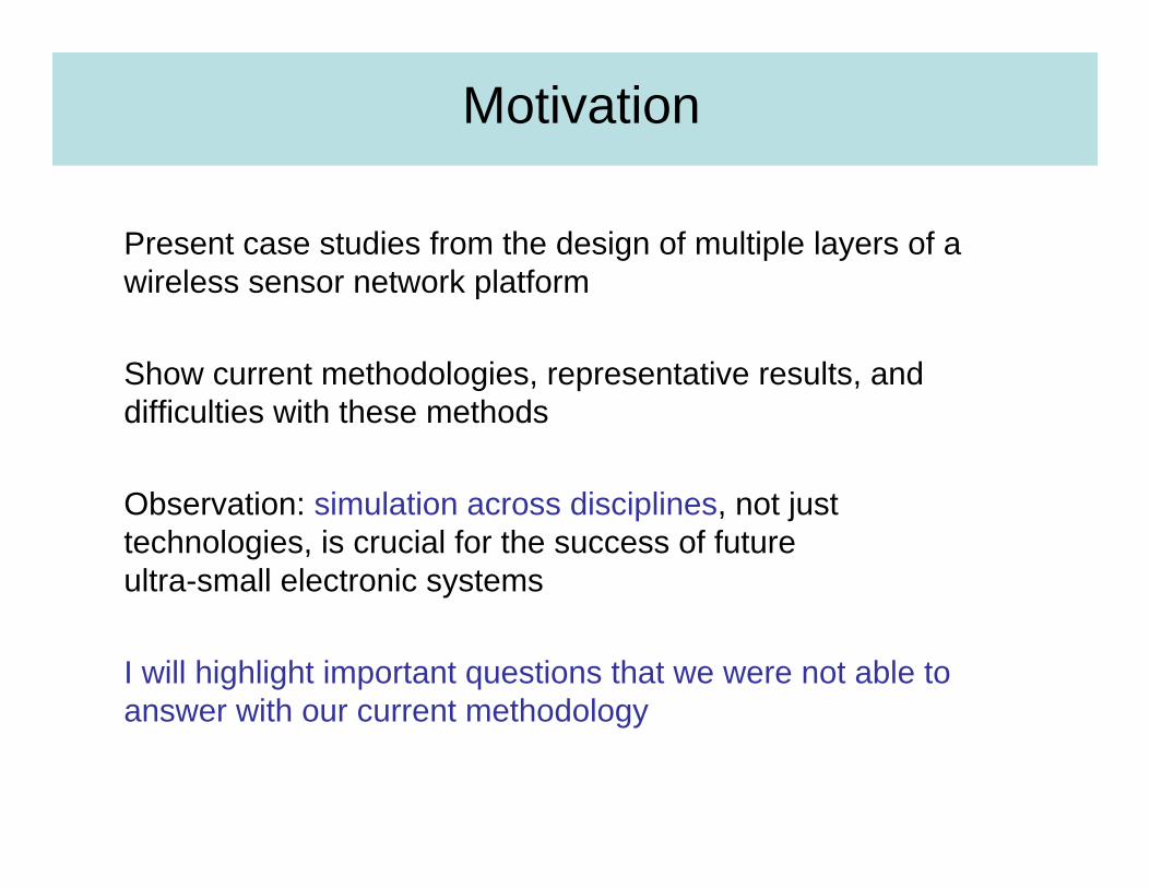
Motivation
Present case studies from the design of multiple layers of a wireless sensor network platform
Show current methodologies, representative results, and difficulties with these methods
Observation: simulation across disciplines, not just technologies, is crucial for the success of future ultra-small electronic systems
I will highlight important questions that we were not able to answer with our current methodology

Application: Wireless Sensing
• Saving energy in building environments
• Tire pressure monitoring
• Wildlife monitoring
• Radiation monitoring
• Biological and implantable devices
Nodes must be small (<1cm3) & self-contained (use energy scavenging)
MEMSVibrationScavenger
MicrobatteryPower Bus
Transceiver,µ-processor
<1cm
This network would allow:
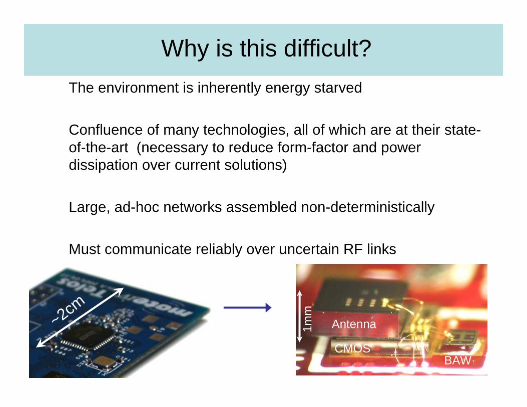
Why is this difficult?The environment is inherently energy starved
Confluence of many technologies, all of which are at their state-of-the-art (necessary to reduce form-factor and power dissipation over current solutions)
Large, ad-hoc networks assembled non-deterministically
Must communicate reliably over uncertain RF links
1mm
BAWCMOS
Antenna~2cm
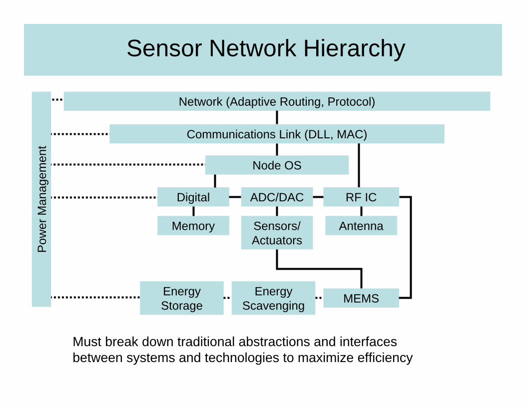
Sensor Network Hierarchy
Network (Adaptive Routing, Protocol)
Node OS
Communications Link (DLL, MAC)
Pow
er M
anag
emen
t
RF ICDigital ADC/DAC
Sensors/Actuators
Antenna
MEMSEnergy Scavenging
Energy Storage
Memory
Must break down traditional abstractions and interfaces between systems and technologies to maximize efficiency
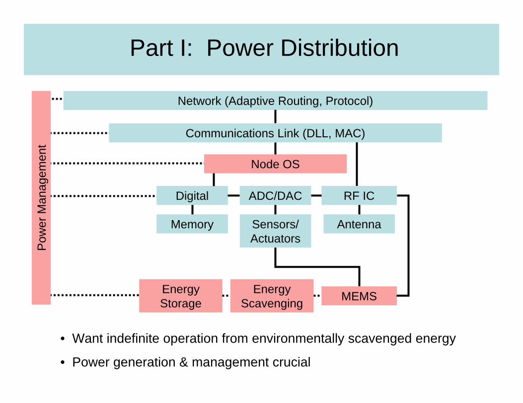
Part I: Power Distribution
Network (Adaptive Routing, Protocol)
Node OS
Communications Link (DLL, MAC)
Pow
er M
anag
emen
t
RF ICDigital ADC/DAC
Sensors/Actuators
Antenna
MEMSEnergy Scavenging
Energy Storage
Memory
• Want indefinite operation from environmentally scavenged energy
• Power generation & management crucial
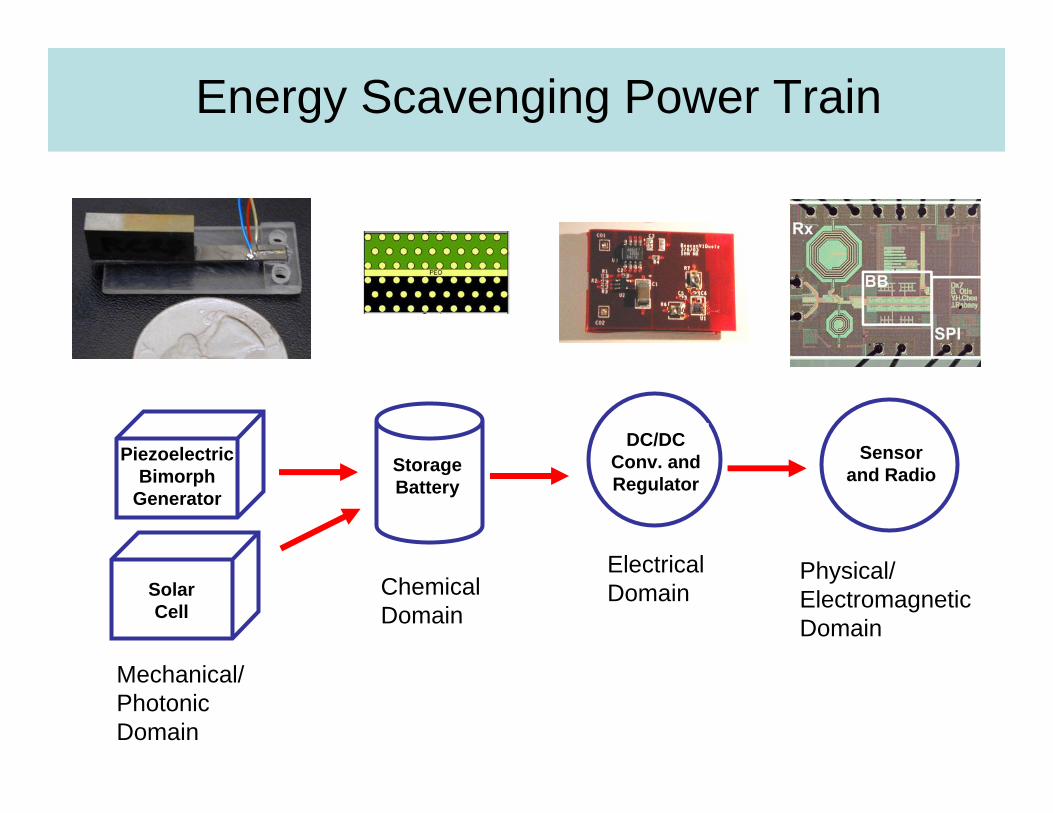
Energy Scavenging Power Train
Sensor and RadioStorage
Battery
ChemicalDomain
Power transfer of 108mW
Piezoelectric Bimorph
Generator
DC/DC Conv. and Regulator
ElectricalDomainSolar
Cell
Physical/ElectromagneticDomain
Mechanical/PhotonicDomain
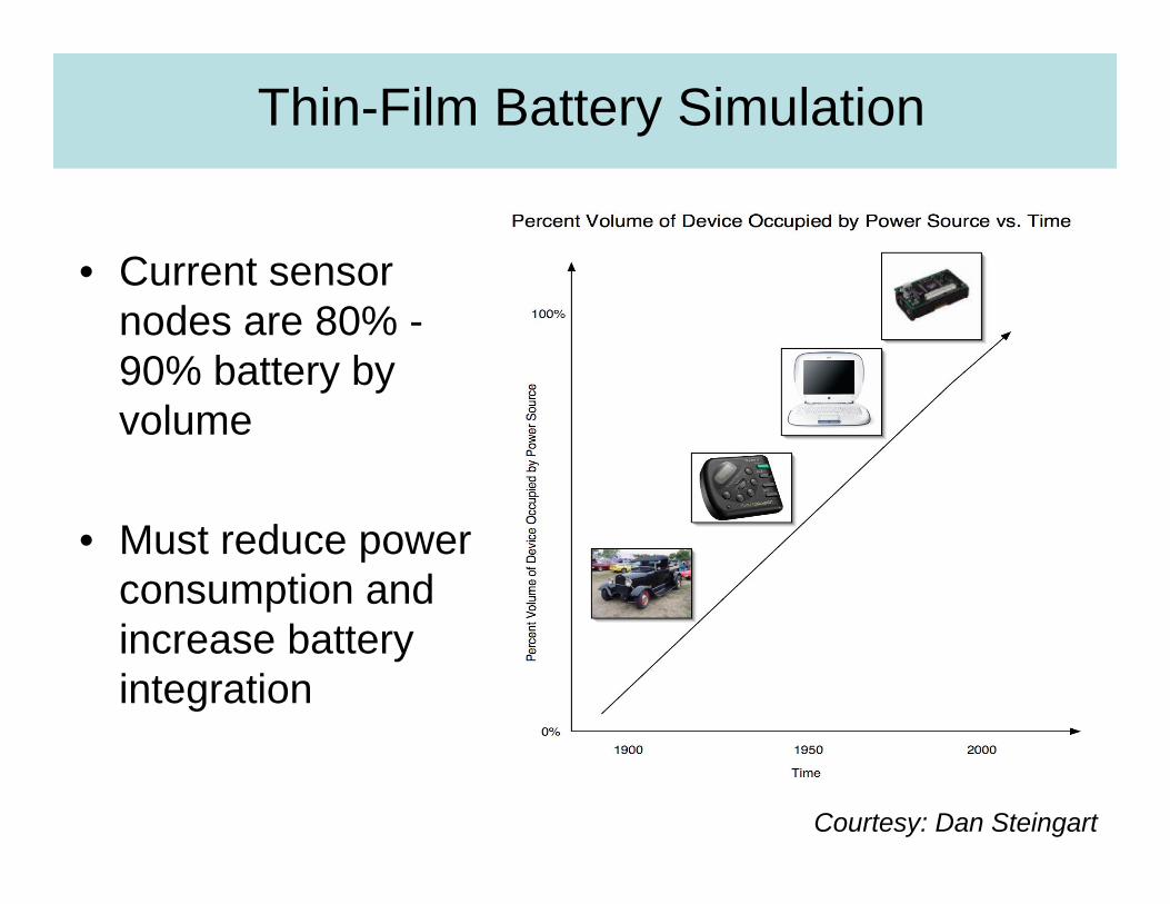
Thin-Film Battery Simulation
• Current sensor nodes are 80% -90% battery by volume
• Must reduce power consumption and increase battery integration
Courtesy: Dan Steingart
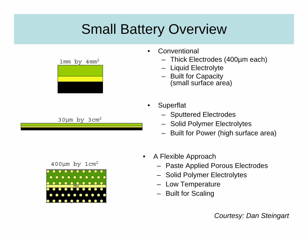
Small Battery Overview• Conventional
– Thick Electrodes (400µm each)– Liquid Electrolyte– Built for Capacity
(small surface area)
• Superflat– Sputtered Electrodes– Solid Polymer Electrolytes– Built for Power (high surface area)
• A Flexible Approach– Paste Applied Porous Electrodes– Solid Polymer Electrolytes– Low Temperature– Built for Scaling
1mm by 4mm2
30µm by 3cm2
400µm by 1cm2
Courtesy: Dan Steingart
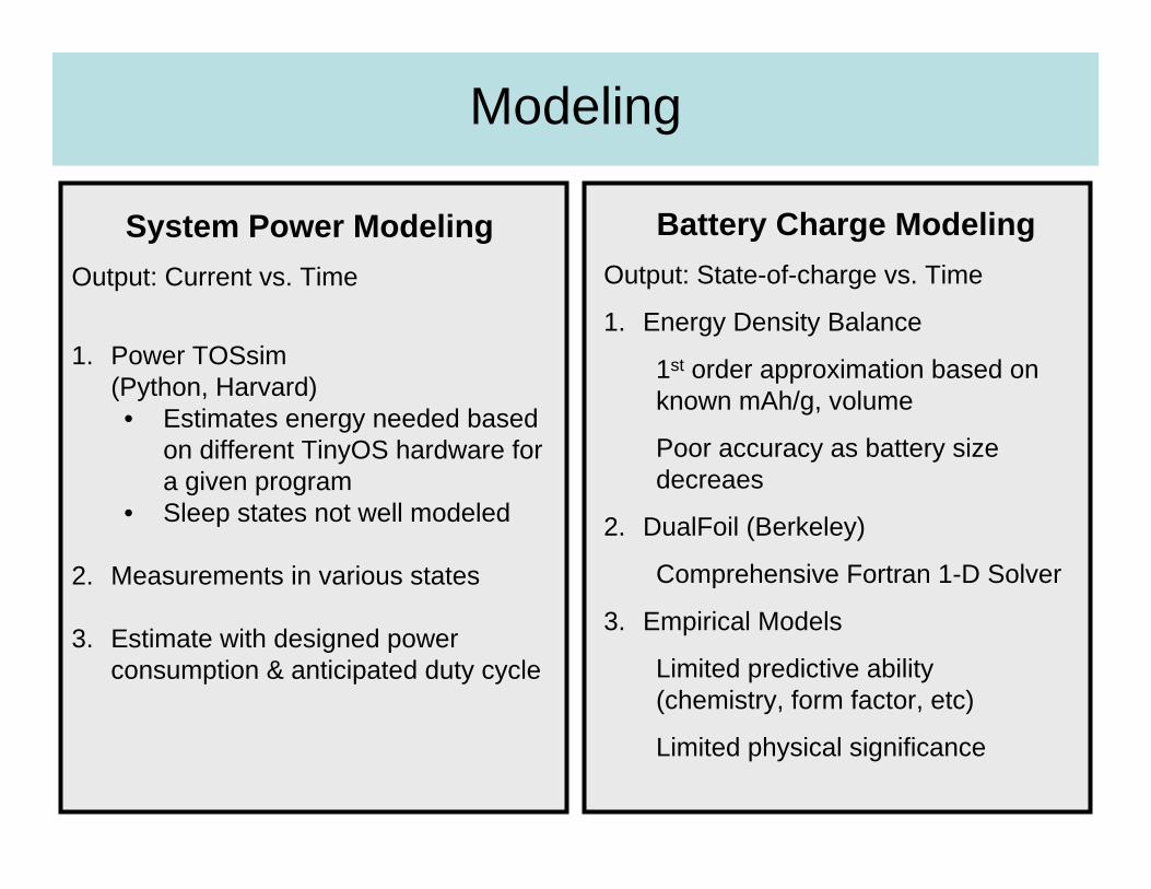
Modeling
System Power ModelingOutput: Current vs. Time
1. Power TOSsim(Python, Harvard)• Estimates energy needed based
on different TinyOS hardware for a given program
• Sleep states not well modeled
2. Measurements in various states
3. Estimate with designed power consumption & anticipated duty cycle
Battery Charge ModelingOutput: State-of-charge vs. Time
1. Energy Density Balance
1st order approximation based on known mAh/g, volume
Poor accuracy as battery size decreaes
2. DualFoil (Berkeley)
Comprehensive Fortran 1-D Solver
3. Empirical Models
Limited predictive ability (chemistry, form factor, etc)
Limited physical significance

Battery Life Simulation
Mica2 Custom Radio
LiCoO2 Li-Ion battery
Simulation setup: PowerTOSsim (Python) to DualFoil (Fortran) controlled via Matlab
Courtesy: Dan SteingartBut, how does the battery state influence network conditions, circuit performance?
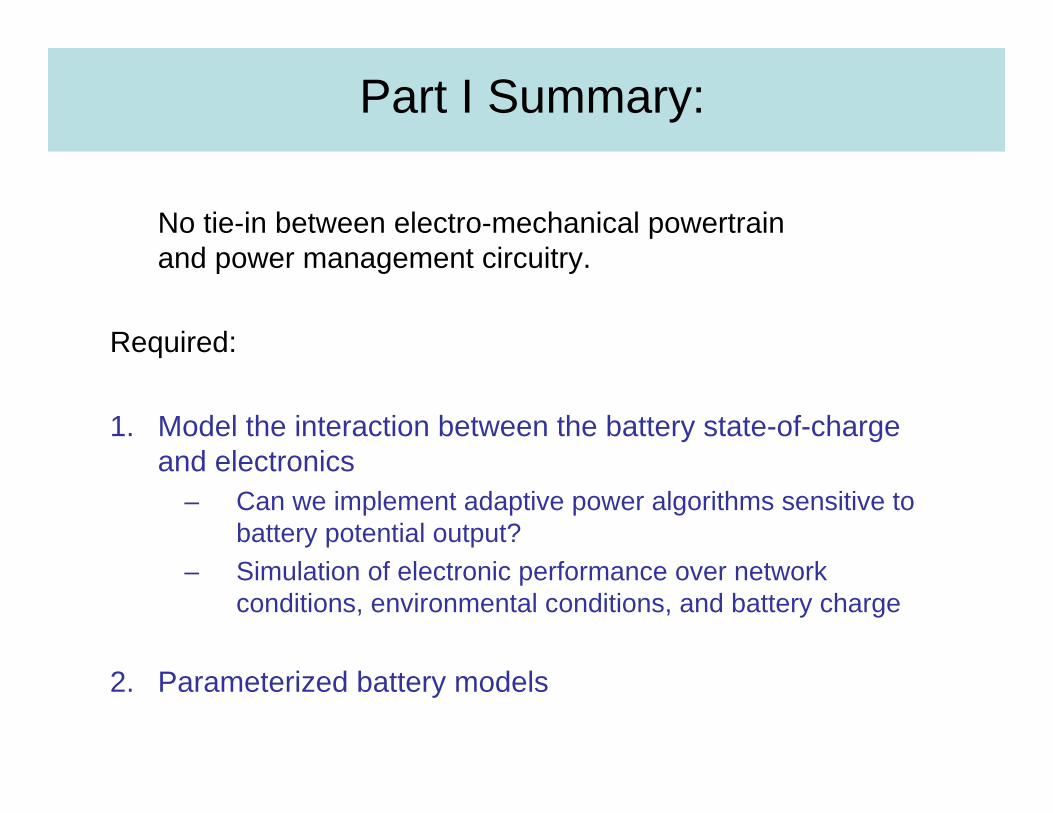
Part I Summary:
No tie-in between electro-mechanical powertrainand power management circuitry.
Required:
1. Model the interaction between the battery state-of-charge and electronics
– Can we implement adaptive power algorithms sensitive to battery potential output?
– Simulation of electronic performance over network conditions, environmental conditions, and battery charge
2. Parameterized battery models

Part II: Communications Link
Network (Adaptive Routing, Protocol)
Node OS
Communications Link (DLL, MAC)
Pow
er M
anag
emen
t
RF ICDigital ADC/DAC
Sensors/Actuators
Antenna
MEMSEnergy Scavenging
Energy Storage
Memory
• Develop efficient network schemes suitable to ad-hoc networks
• Huge gains in efficiency can occur at higher network layers

Communication Link: Protocol Stack
Step 1: Design, modeling and analysis
Step 2: Simulation (Omnet++)
Step 3: Implementation (Berkeley motes)
Courtesy: R. Shah
The design included opportunistic routing, pseudo-asynchronous MAC and adaptive duty cycling.
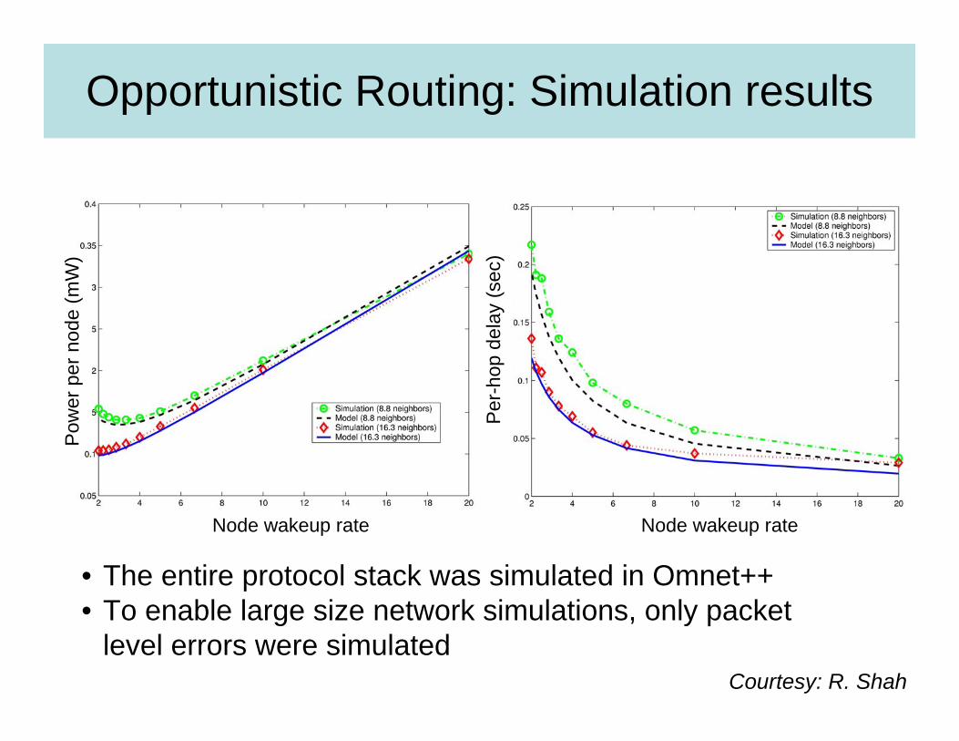
Opportunistic Routing: Simulation results
Node wakeup rate
Pow
er p
er n
ode
(mW
)
Node wakeup rateP
er-h
op d
elay
(sec
)
• The entire protocol stack was simulated in Omnet++• To enable large size network simulations, only packet
level errors were simulatedCourtesy: R. Shah
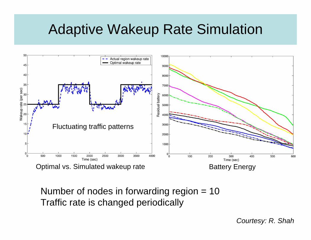
Adaptive Wakeup Rate Simulation
Number of nodes in forwarding region = 10Traffic rate is changed periodically
Battery EnergyOptimal vs. Simulated wakeup rate
Courtesy: R. Shah
Fluctuating traffic patterns
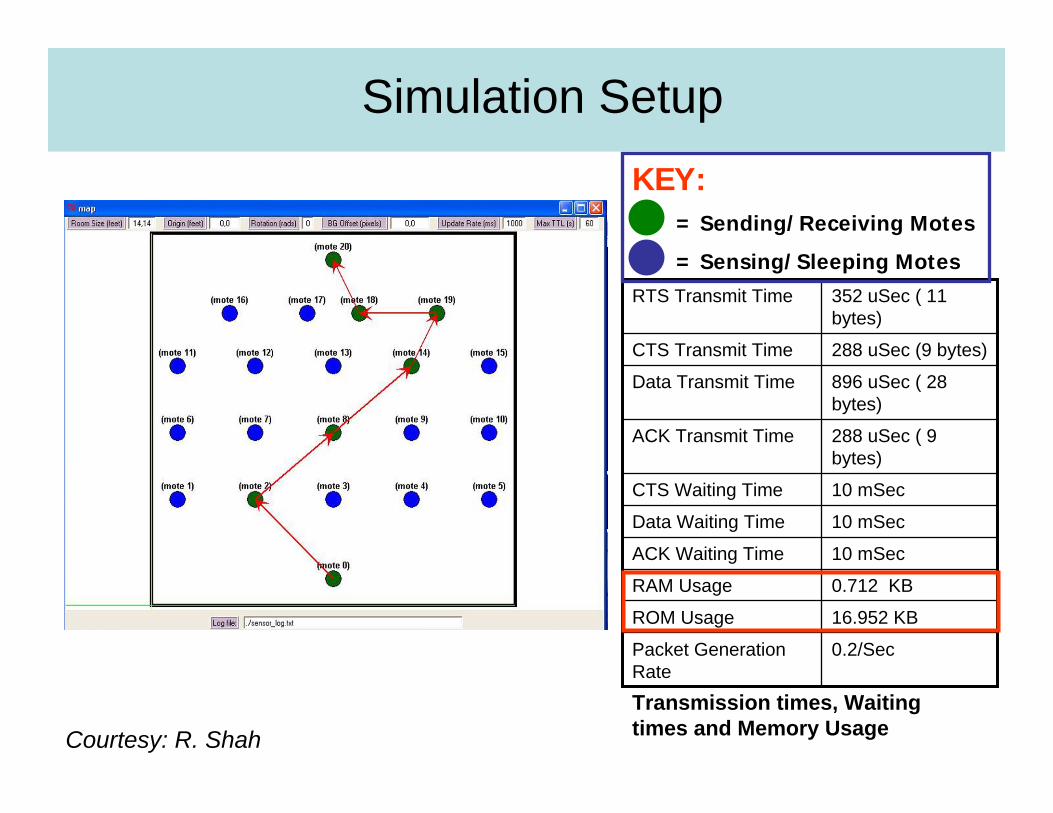
Simulation Setup
16.952 KBROM Usage
0.712 KBRAM Usage
0.2/SecPacket Generation Rate
10 mSecACK Waiting Time
10 mSecData Waiting Time
10 mSecCTS Waiting Time
288 uSec ( 9 bytes)
ACK Transmit Time
896 uSec ( 28 bytes)
Data Transmit Time
288 uSec (9 bytes)CTS Transmit Time
352 uSec ( 11 bytes)
RTS Transmit Time
Transmission times, Waiting times and Memory Usage
KEY:= Sending/Receiving Motes
= Sensing/Sleeping Motes
Courtesy: R. Shah
Part II Summary:
Protocol/MAC designed via analysis/simulation
No connection to physical layer models, so joint optimization not possible
How much power is used during network discovery, etc?
How does changing the modulation scheme or transmitted power effect overall network performance?
How does the adaptive wakeup rate perform with a physical battery model?
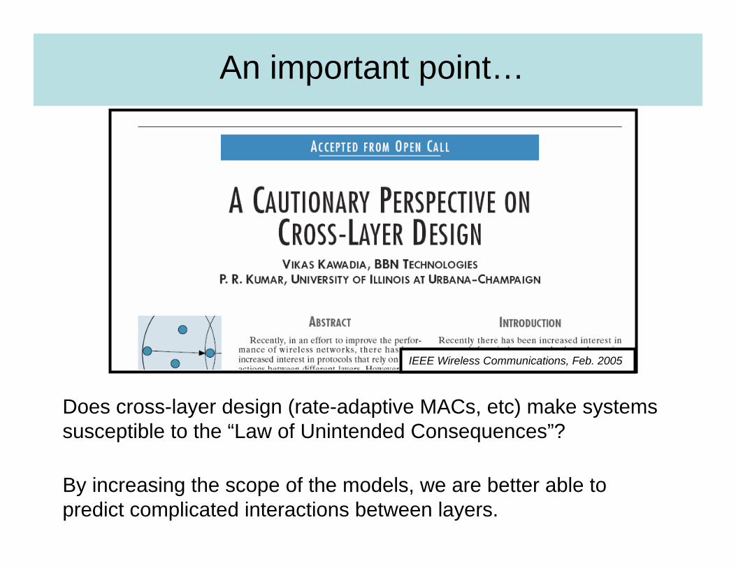
An important point…
Does cross-layer design (rate-adaptive MACs, etc) make systems susceptible to the “Law of Unintended Consequences”?
By increasing the scope of the models, we are better able to predict complicated interactions between layers.
IEEE Wireless Communications, Feb. 2005
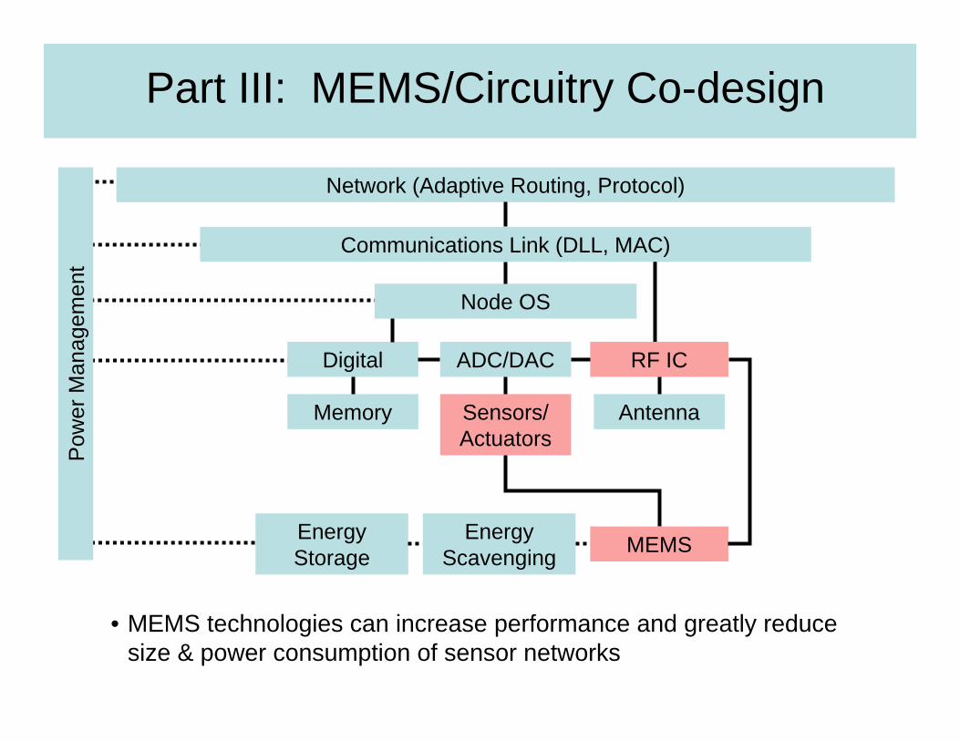
Part III: MEMS/Circuitry Co-design
Network (Adaptive Routing, Protocol)
Node OS
Communications Link (DLL, MAC)
Pow
er M
anag
emen
t
RF ICDigital ADC/DAC
Sensors/Actuators
Antenna
MEMSEnergy Scavenging
Energy Storage
Memory
• MEMS technologies can increase performance and greatly reduce size & power consumption of sensor networks
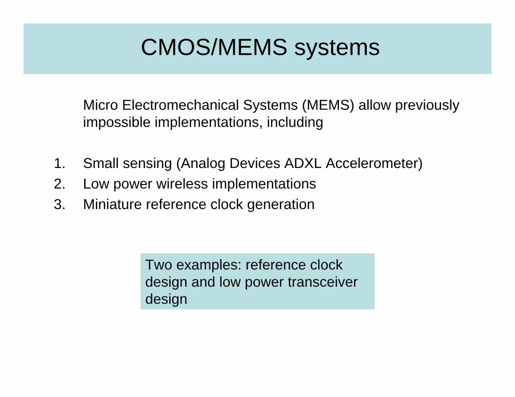
CMOS/MEMS systems
Micro Electromechanical Systems (MEMS) allow previously impossible implementations, including
1. Small sensing (Analog Devices ADXL Accelerometer)2. Low power wireless implementations3. Miniature reference clock generation
Two examples: reference clock design and low power transceiver design
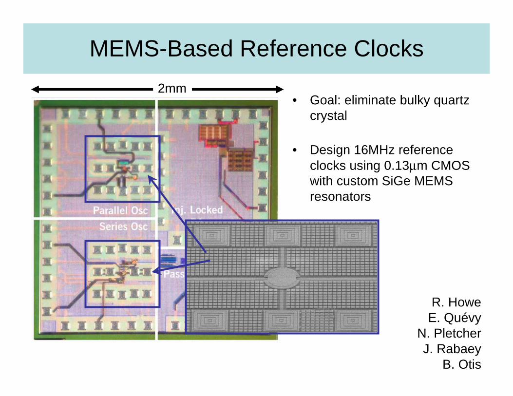
MEMS-Based Reference Clocks
• Goal: eliminate bulky quartz crystal
• Design 16MHz reference clocks using 0.13µm CMOS with custom SiGe MEMS resonators
2mm
R. HoweE. Quévy
N. PletcherJ. Rabaey
B. Otis
hLWTLTF
TLTETI
fSiGe
M
est ....389.0)()(.89.4
)()().(.199
.21 3
mod1 ρπ
+=
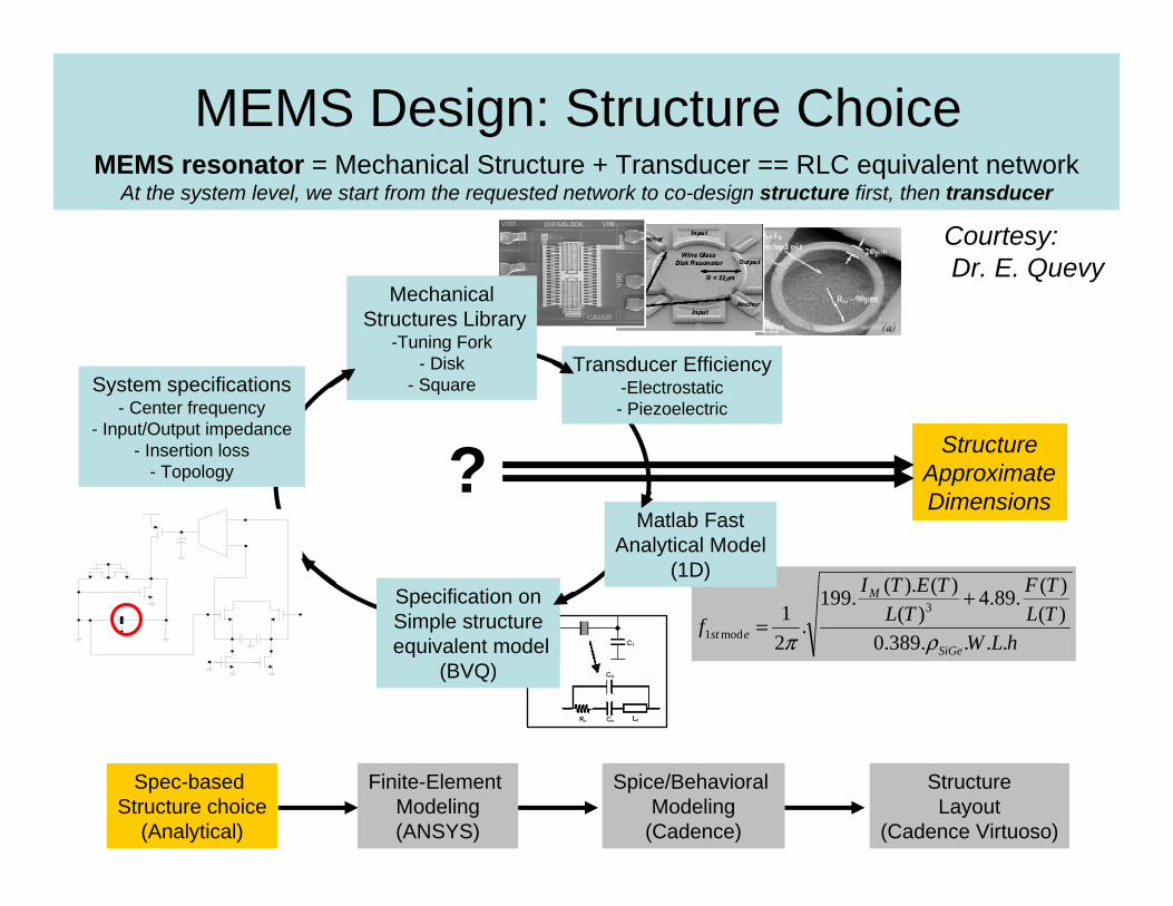
MechanicalStructures Library
-Tuning Fork- Disk
- Square
Matlab FastAnalytical Model
(1D)
MEMS Design: Structure Choice
Specification onSimple structureequivalent model
(BVQ)
MEMS resonator = Mechanical Structure + Transducer == RLC equivalent networkAt the system level, we start from the requested network to co-design structure first, then transducer
Transducer Efficiency-Electrostatic- Piezoelectric
Spec-based Structure choice
(Analytical)
Finite-Element Modeling(ANSYS)
Spice/Behavioral Modeling
(Cadence)
StructureLayout
(Cadence Virtuoso)
StructureApproximateDimensions
?System specifications
- Center frequency- Input/Output impedance
- Insertion loss- Topology
Courtesy: Dr. E. Quevy
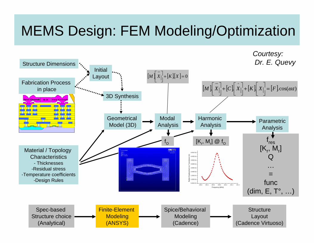
Geometrical Model (3D)
MEMS Design: FEM Modeling/Optimization
[ ] [ ][ ] 0. =+⎥⎦⎤
⎢⎣⎡ °°
XKXM
Material / Topology Characteristics
- Thicknesses-Residual stress
-Temperature coefficients-Design Rules
Structure Dimensions
BLRDrive Electrode Sense Electrode
Microshell Encapsulation(anchors not shown)
BLRDrive Electrode Sense Electrode
Microshell Encapsulation(anchors not shown)
Spec-based Structure choice
(Analytical)
Finite-Element Modeling(ANSYS)
Spice/Behavioral Modeling
(Cadence)
StructureLayout
(Cadence Virtuoso)
Modal Analysis
Harmonic Analysis
ParametricAnalysis
InitialLayout
3D Synthesis
Fabrication Process in place [ ] [ ] [ ] [ ] ).cos(.... tFXKXCXM ω=⎥⎦
⎤⎢⎣⎡+⎥⎦
⎤⎢⎣⎡+⎥⎦
⎤⎢⎣⎡ °°°
fres[Kr, Mr]
Q…=
func(dim, E, T°, …)
[Kr, Mr] @ fOfO
100.2 100.4 100.6 100.8 101.0 101.2 101.45.00E-012
1.00E-011
1.50E-011
2.00E-011
2.50E-011
3.00E-011
3.50E-011
4.00E-011
4.50E-011
Rad
ial D
ispl
acem
ent o
n Tr
ansd
ucer
(m)
Frequency (MHz)
Courtesy: Dr. E. Quevy
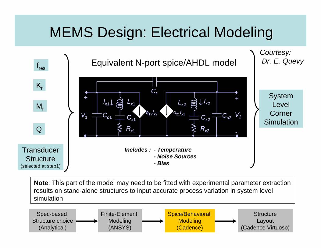
MEMS Design: Electrical Modeling
Spec-based Structure choice
(Analytical)
Finite-Element Modeling(ANSYS)
Spice/Behavioral Modeling
(Cadence)
StructureLayout
(Cadence Virtuoso)
Includes : - Temperature- Noise Sources- Bias
System Level
Corner Simulation
fres
Kr
Mr
Q
TransducerStructure
(selected at step1)
Cx1
Lx1
Rx1
Co1
→
Ix1+
-
V1φ21Ix1
+
-
V2φ12Ix2 Cx2
Lx2
Rx2
Ix2
→Co2
Cf
Cx1
Lx1
Rx1
Co1
→
Ix1+
-
V1φ21Ix1
+
-
V2φ12Ix2 Cx2
Lx2
Rx2
Ix2
→Co2
Cf
Equivalent N-port spice/AHDL model
Note: This part of the model may need to be fitted with experimental parameter extraction results on stand-alone structures to input accurate process variation in system level simulation
Courtesy: Dr. E. Quevy
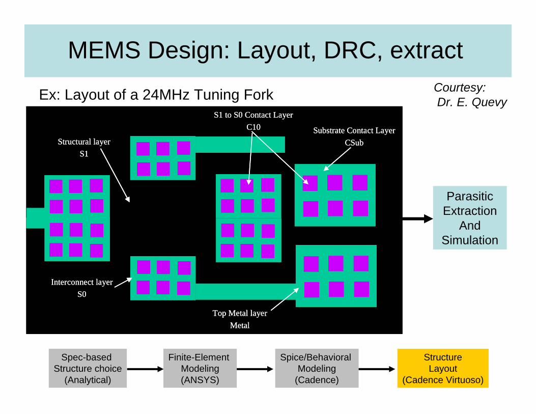
MEMS Design: Layout, DRC, extract
Spec-based Structure choice
(Analytical)
Finite-Element Modeling(ANSYS)
Spice/Behavioral Modeling
(Cadence)
StructureLayout
(Cadence Virtuoso)
Substrate Contact LayerCSub
Top Metal layerMetal
Structural layerS1
Interconnect layerS0
S1 to S0 Contact LayerC10 Substrate Contact Layer
CSub
Top Metal layerMetal
Structural layerS1
Interconnect layerS0
S1 to S0 Contact LayerC10
Ex: Layout of a 24MHz Tuning Fork
ParasiticExtraction
AndSimulation
Courtesy: Dr. E. Quevy
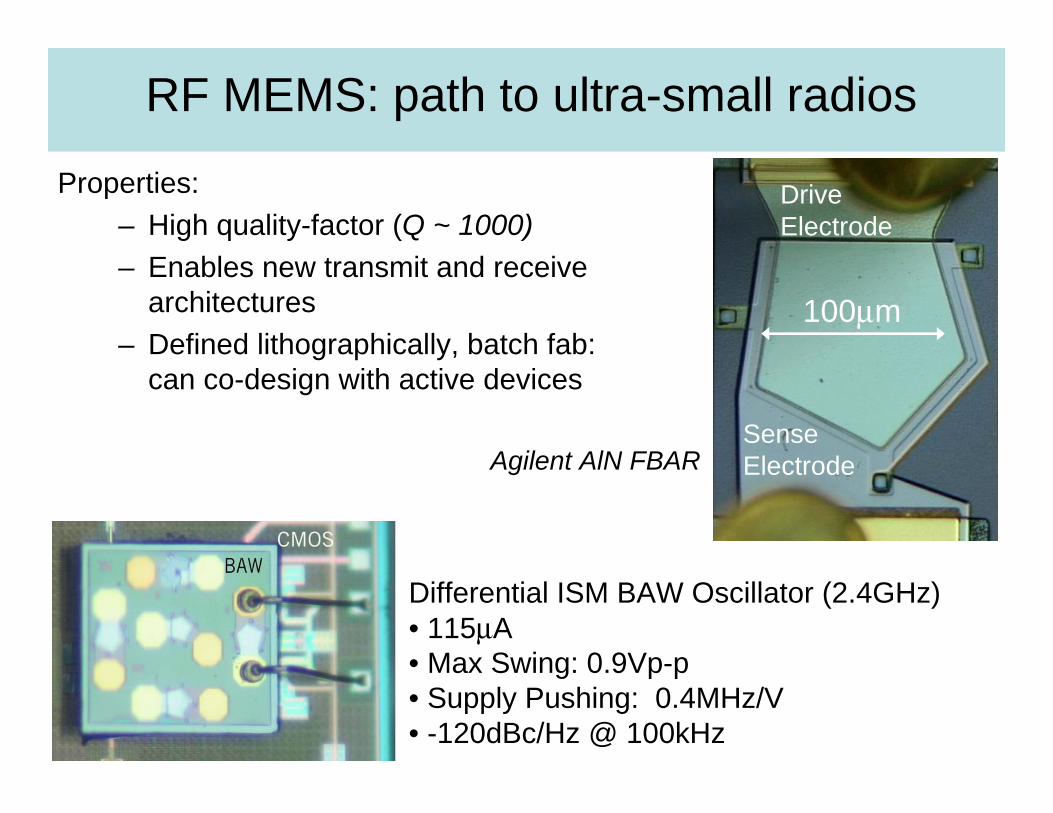
RF MEMS: path to ultra-small radios
Drive Electrode
Sense Electrode
100µm
Properties:– High quality-factor (Q ~ 1000)– Enables new transmit and receive
architectures– Defined lithographically, batch fab:
can co-design with active devices
Agilent AlN FBAR
Differential ISM BAW Oscillator (2.4GHz)• 115µA• Max Swing: 0.9Vp-p• Supply Pushing: 0.4MHz/V• -120dBc/Hz @ 100kHz

Rx
Rp
BAW/CMOS Co-Design
• Can control resonatorparameters lithographically
• Co-design MEMS/circuit to achieve optimal performance
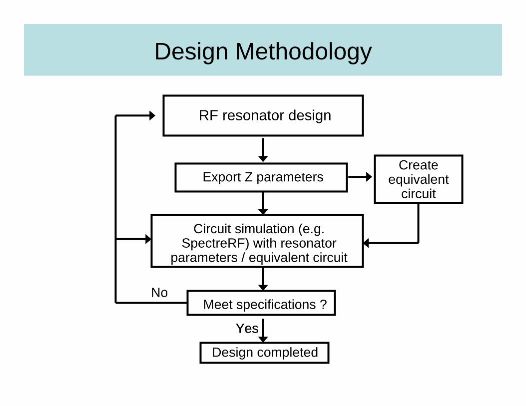
Design Methodology
RF resonator design
Export Z parameters
Circuit simulation (e.g. SpectreRF) with resonator
parameters / equivalent circuit
Create equivalent
circuit
Meet specifications ?
Yes
Design completed
Yes
No
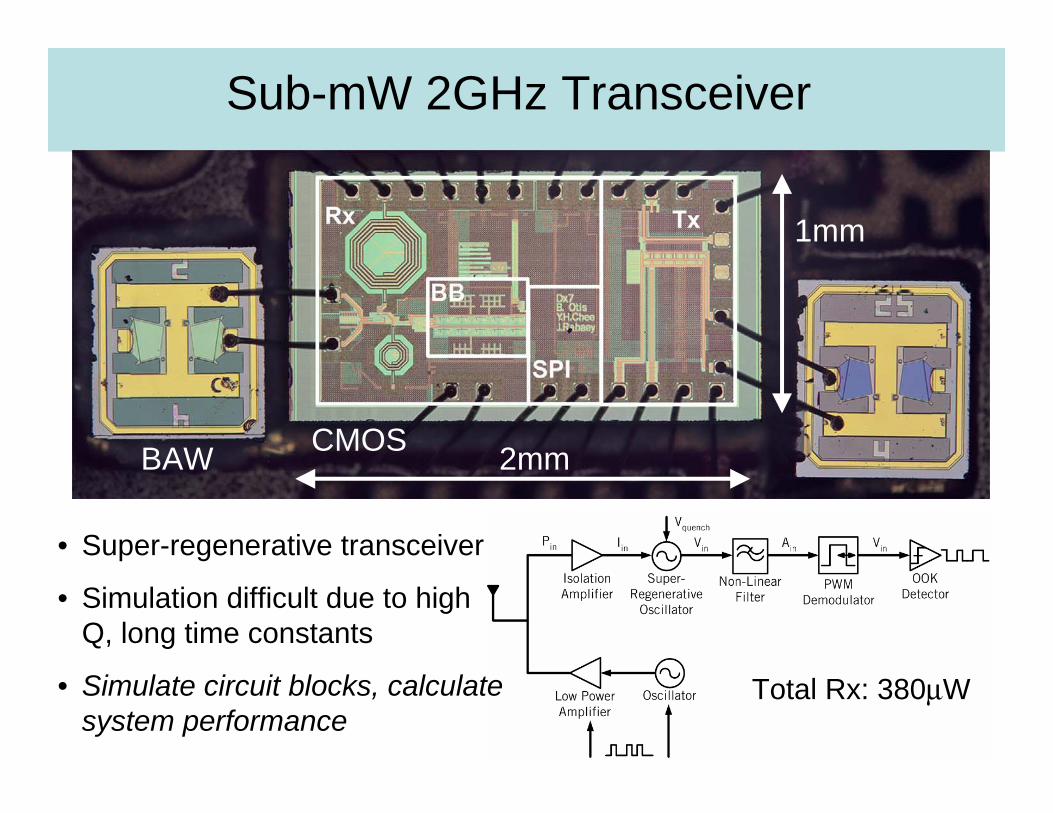
Sub-mW 2GHz Transceiver
• Super-regenerative transceiver
• Simulation difficult due to high Q, long time constants
• Simulate circuit blocks, calculate system performance
2mm
Total Rx: 380µW
1mm
BAW CMOS
Part III Summary:
• Silicon MEMS technology will become more pervasive in electronic systems
• Currently, no parametric SPICE models for these components
• RF MEMS devices provide very high fosc* Q products:– Allows reduced transceiver power consumption– Greatly increases simulation difficulty
• Non-linear super-regenerative receiver difficult to simulate
• Simulating entire receive chain over an entire packet training sequence very time/CPU intensive
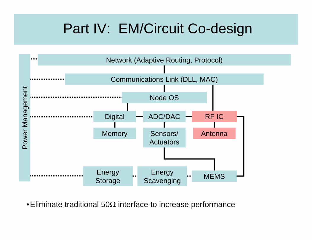
Part IV: EM/Circuit Co-design
Network (Adaptive Routing, Protocol)
Node OS
Communications Link (DLL, MAC)
Pow
er M
anag
emen
t
RF ICDigital ADC/DAC
Sensors/Actuators
Antenna
MEMSEnergy Scavenging
Energy Storage
Memory
•Eliminate traditional 50Ω interface to increase performance
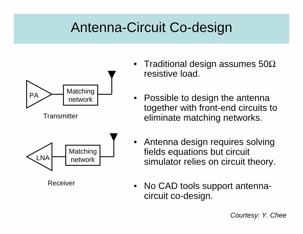
Antenna-Circuit Co-design
• Traditional design assumes 50Ωresistive load.
• Possible to design the antenna together with front-end circuits to eliminate matching networks.
• Antenna design requires solving fields equations but circuit simulator relies on circuit theory.
• No CAD tools support antenna-circuit co-design.
Matching networkPA
Matching networkLNA
Transmitter
Receiver
Courtesy: Y. Chee

High Frequency Structure Simulator (HFSS)
• HFSS is a full 3-D EM simulator.• Use to simulate antenna input impedance, radiation pattern
and efficiency.• Able to export S, Y or Z port parameters.
RadiationPattern
Courtesy: Y. Chee

Design Methodology
Antenna design using EM simulator (e.g HFSS)
Export S,Y,Z parameters
Circuit simulation (e.g. spectreRF) with antenna port parameters / equivalent circuit
Create equivalent
circuit
Meet specifications ?
Yes
Design completed
Yes
No
Courtesy: Y. Chee

Part IV Summary:
Typically, there is a clean 50Ω handoff between RF circuit designers and microwave antenna designers
The co-design of electromagnetic transducers and integrated circuits can improve the efficiency of RF links
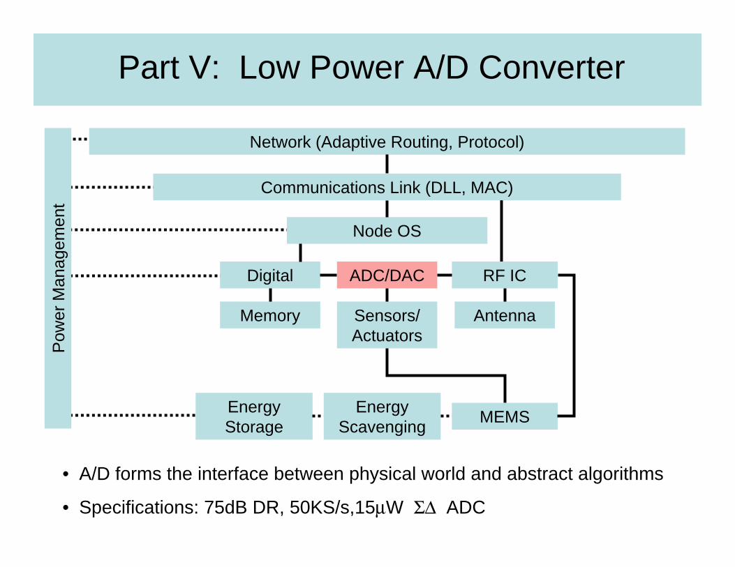
Part V: Low Power A/D Converter
Network (Adaptive Routing, Protocol)
Node OS
Communications Link (DLL, MAC)
Pow
er M
anag
emen
t
RF ICDigital ADC/DAC
Sensors/Actuators
Antenna
MEMSEnergy Scavenging
Energy Storage
Memory
• A/D forms the interface between physical world and abstract algorithms
• Specifications: 75dB DR, 50KS/s,15µW Σ∆ ADC
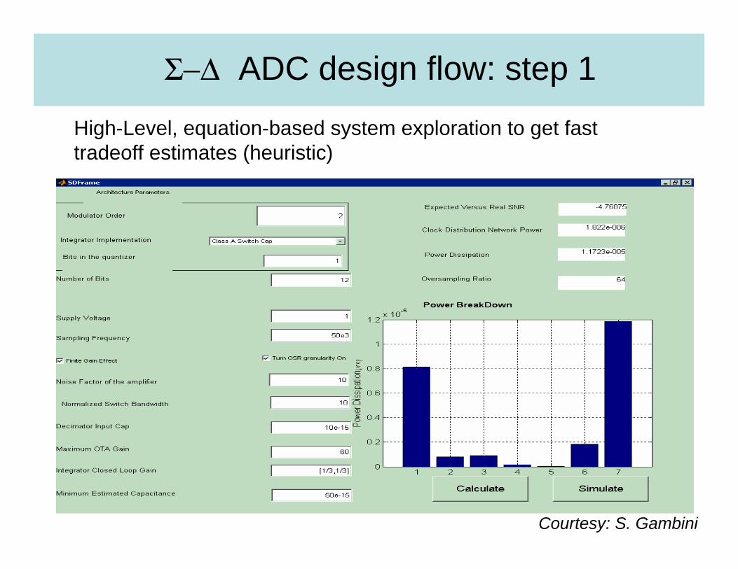
Σ−∆ ADC design flow: step 1High-Level, equation-based system exploration to get fast tradeoff estimates (heuristic)
Courtesy: S. Gambini
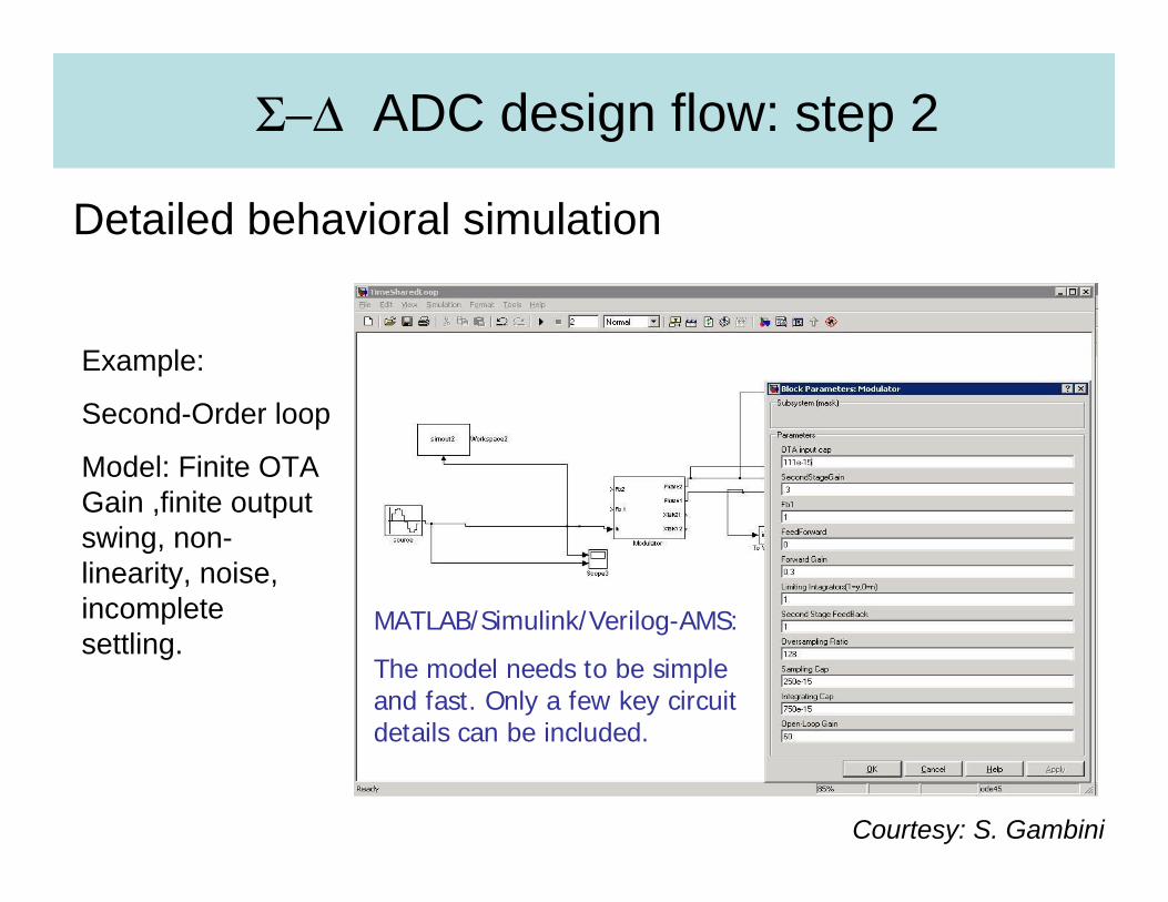
Σ−∆ ADC design flow: step 2
Detailed behavioral simulation
MATLAB/Simulink/Verilog-AMS:
The model needs to be simple and fast. Only a few key circuit details can be included.
Example:
Second-Order loop
Model: Finite OTA Gain ,finite output swing, non-linearity, noise, incomplete settling.
Courtesy: S. Gambini
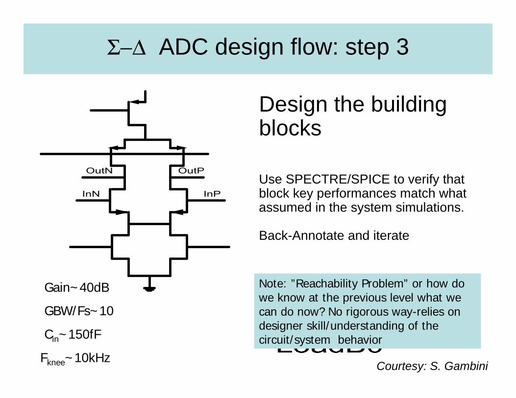
Σ−∆ ADC design flow: step 3
Design the building blocks
Use SPECTRE/SPICE to verify that block key performances match what assumed in the system simulations.
Back-Annotate and iterate
Note: ”Reachability Problem” or how do we know at the previous level what we can do now? No rigorous way-relies on designer skill/understanding of the circuit/system behavior
Gain~40dB
GBW/Fs~10
Cin~150fF
Fknee~10kHzCourtesy: S. Gambini

Σ−∆ ADC design flow: step 3
• Digital Programmability
Example: Bias tuning
5-bit tuning range allows compensation for process variation and operation at variable sampling frequency and dynamic range
Limit overdesign by adding on-chip programmability
Courtesy: S. Gambini
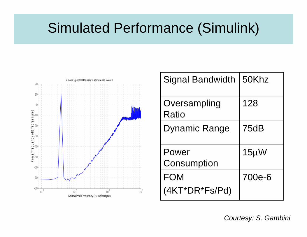
Simulated Performance (Simulink)
700e-6FOM(4KT*DR*Fs/Pd)
15µWPower Consumption
75dBDynamic Range
128OversamplingRatio
50KhzSignal Bandwidth
10-3 10-2 10-1 100-80
-70
-60
-50
-40
-30
-20
-10
0
10
20
Normalized Frequency (×π rad/sample)
Pow
er/fr
eque
ncy
(dB
/rad/
sam
ple)
Power Spectral Density Estimate via Welch
Courtesy: S. Gambini
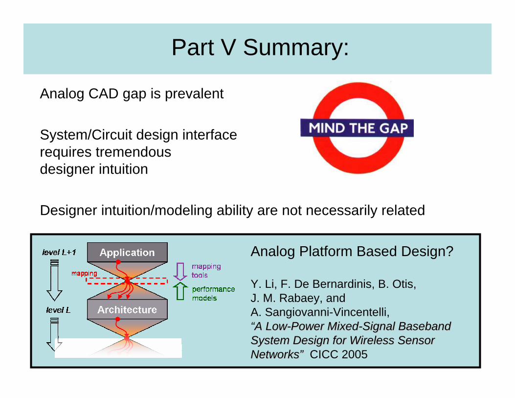
Part V Summary:
Analog CAD gap is prevalent
System/Circuit design interfacerequires tremendous designer intuition
Designer intuition/modeling ability are not necessarily related
Analog Platform Based Design?
Y. Li, F. De Bernardinis, B. Otis, J. M. Rabaey, and A. Sangiovanni-Vincentelli, “A LowA Low--Power MixedPower Mixed--Signal Signal BasebandBasebandSystem Design for Wireless Sensor System Design for Wireless Sensor NetworksNetworks”” CICC 2005

Conclusions
1. Electronics are becoming vanishingly small and truly ubiquitous
2. The convergence of many different disciplines is needed for ultra-small, low power electronic systems
3. Future chips will include transistors, EM elements, MEMS structures, biological sensors, thin-film batteries, adaptive algorithms.. all designed together
500µm
4. Seamless simulation between systems is necessary to allow cross-discipline co-design (and protect against the “Law of Unintended Consequences”)