Embed Size (px)
Citation preview
UBX-19033350 - R26
C1-Public www.u-blox.com
BMD-300 Stand-alone Bluetooth low energy module Data sheet
Abstract
This technical data sheet describes the BMD-300 stand-alone Bluetooth® low energy module. The
OEMs can embed their own application on top of the integrated Bluetooth low energy stack using
Nordic Semiconductor SDK integrated development environment (IDE).

BMD-300 - Data sheet
UBX-19033350 - R26 Document information Page 2 of 37
C1-Public
Document information
Title BMD-300
Subtitle Stand-alone Bluetooth low energy module
Document type Data sheet
Document number UBX-19033350
Revision and date R26 19-Jul-2021
Disclosure restriction C1-Public
Product status Corresponding content status
Functional sample Draft For functional testing. Revised and supplementary data will be published later.
In development /
Prototype
Objective specification Target values. Revised and supplementary data will be published later.
Engineering sample Advance information Data based on early testing. Revised and supplementary data will be published later.
Initial production Early production information Data from product verification. Revised and supplementary data may be published later.
Mass production /
End of life
Production information Document contains the final product specification.
This document applies to the following products:
Product name Type number Firmware version IN/PCN reference Product status
BMD-300 BMD-300-A-R-00 All UBX-19039722 Mass production
BMD-300 BMD-300-A-R-10 AE UBX-20007336 Mass production
BMD-300 BMD-300-A-R-20 AE UBX-21028574 Initial production
u-blox or third parties may hold intellectual property rights in the products, names, logos, and designs included in this
document. Copying, reproduction, modification, or disclosure to third parties of this document or any part thereof is only
permitted with the express written permission of u-blox.
The information contained herein is provided “as is” and u-blox assumes no liability for its use. No warranty, either express or
implied, is given, including but not limited to, with respect to the accuracy, correctness, reliability, and fitness for a particular
purpose of the information. This document may be revised by u-blox at any time without notice. For the most recent
documents, visit www.u-blox.com.
Copyright © u-blox AG.
BMD-300 - Data sheet
UBX-19033350 - R26 Contents Page 3 of 37
C1-Public
Contents Document information ............................................................................................................................. 2
Contents ....................................................................................................................................................... 3
1 Functional description ....................................................................................................................... 5
Features ........................................................................................................................................................ 5
Applications ................................................................................................................................................. 5
Block diagram .............................................................................................................................................. 6
Product specifications ............................................................................................................................... 7
2 Pin definition......................................................................................................................................... 9
Pin assignment ............................................................................................................................................ 9
Peripheral pin assignments .................................................................................................................... 10
3 Electrical specifications ................................................................................................................. 12
Absolute maximum ratings .................................................................................................................... 12
Operating conditions ................................................................................................................................ 12
General purpose I/O .................................................................................................................................. 12
3.4 Peripheral pin assignments .................................................................................................................... 13
Module reset .............................................................................................................................................. 13
Debug and programming ......................................................................................................................... 13
Clocks .......................................................................................................................................................... 13
3.7.1 32.768 kHz crystal (LFXO) .............................................................................................................. 14
3.7.2 32.768 kHz clock source comparison ........................................................................................... 14
4 Firmware ............................................................................................................................................. 15
Factory image ............................................................................................................................................ 15
4.1.1 Firmware version “AA” ..................................................................................................................... 15
4.1.2 Firmware version “AB” ..................................................................................................................... 15
4.1.3 Firmware version “AC” ..................................................................................................................... 15
4.1.4 Firmware version “AD” ..................................................................................................................... 16
4.1.5 Firmware version “AE” ..................................................................................................................... 16
Module programming and read-back protection ............................................................................... 16
SoftDevices ................................................................................................................................................ 16
4.3.1 S132 .................................................................................................................................................... 17
4.3.2 S212 .................................................................................................................................................... 17
4.3.3 S332 .................................................................................................................................................... 17
Bluetooth device address ........................................................................................................................ 17
5 Mechanical specifications ............................................................................................................. 18
Dimensions ................................................................................................................................................. 18
Recommended PCB land pads ............................................................................................................... 18
Module marking ......................................................................................................................................... 19
5.3.1 BMD-300-A-R-00 module marking ............................................................................................... 19
5.3.2 BMD-300-A-R-10 and BMD-300-A-R-20 module marking ...................................................... 20
6 RF design notes ................................................................................................................................ 21

BMD-300 - Data sheet
UBX-19033350 - R26 Contents Page 4 of 37
C1-Public
Recommended RF layout and ground plane ........................................................................................ 21
Mechanical enclosure ............................................................................................................................... 21
Antenna patterns ...................................................................................................................................... 22
6.3.1 X-Y plane ............................................................................................................................................. 22
6.3.2 X-Z plane ............................................................................................................................................. 23
6.3.3 Y-Z plane ............................................................................................................................................ 23
7 BMD-300 evaluation development kit ....................................................................................... 24
8 Qualification and approvals .......................................................................................................... 25
United States (FCC): ................................................................................................................................ 25
8.1.1 Labeling and user information requirements ............................................................................. 25
8.1.2 RF exposure ....................................................................................................................................... 25
Canada (ISED) ............................................................................................................................................ 26
8.2.1 Labeling and user information requirements ............................................................................. 26
8.2.2 RF exposure ....................................................................................................................................... 26
European Union regulatory compliance ............................................................................................... 27
8.3.1 Radio Equipment Directive (RED) 2014/53/EU .......................................................................... 27
8.3.2 Labeling and user information requirements ............................................................................. 27
Japan (MIC) ................................................................................................................................................ 27
Australia / New Zealand (RCM) .............................................................................................................. 27
South Korea (KCC) .................................................................................................................................... 28
Brazil (ANATEL) ......................................................................................................................................... 28
Mexico (IFETEL) ........................................................................................................................................ 28
Bluetooth qualification ............................................................................................................................. 28
9 Environmental ................................................................................................................................... 29
RoHS ............................................................................................................................................................ 29
REACH ......................................................................................................................................................... 29
California proposition 65 (P65) .............................................................................................................. 29
10 Product handling .............................................................................................................................. 30
Packaging ................................................................................................................................................... 30
10.1.1 BMD-300-A-R-00 reel packaging .................................................................................................. 30
10.1.2 BMD-300-A-R-10 and BMD-300-A-R-20 reel packaging ......................................................... 30
10.1.3 BMD-300-A-R-00 carrier tape dimensions .................................................................................. 31
10.1.4 BMD-300-A-R-10 and BMD-300-A-R-20 carrier tape dimensions ......................................... 31
Moisture sensitivity level ......................................................................................................................... 31
Reflow soldering ........................................................................................................................................ 32
ESD precautions ........................................................................................................................................ 32
11 Ordering information ...................................................................................................................... 33
12 Life support and other high-risk warnings ............................................................................... 34
Related documents ................................................................................................................................ 35
Revision history ....................................................................................................................................... 35
Contact ....................................................................................................................................................... 37
BMD-300 - Data sheet
UBX-19033350 - R26 Functional description Page 5 of 37
C1-Public
1 Functional description The BMD-300 is a powerful, highly flexible, ultra-low power Bluetooth low energy module based on the
nRF52832 SoC from Nordic Semiconductor. With an Arm® Cortex®-M4 with FPU 32-bit processor,
embedded 2.4GHz transceiver, and integrated antenna, the BMD-300 provides a complete RF
solution with no additional RF design, allowing faster time to market. Providing full use of the
nRF52832’s capabilities and peripherals, the BMD-300 can power the most demanding applications,
all while simplifying designs and reducing BOM costs. With an internal DC-DC converter and
intelligent power control, the BMD-300 provides class-leading power efficiency, enabling ultra-low
power sensitive applications. Regulatory pre-approvals reduce the burden to enter the market.
Features
• Based on the Nordic Semiconductor nRF52832 SoC
• Bluetooth 5 PHYs: LE 1M, LE 2M
• Bluetooth 5 features: Advertising Extensions, Channel Selection Algorithm #2
• Bluetooth mesh
• Complete RF solution with an integrated DC-DC converter
• Nordic Semiconductor SoftDevice ready
• Over-the-Air (OTA) firmware updates
• No external components required
• Arm® Cortex®-M4 with FPU 32-bit processor
• 512 kB embedded flash memory
• 64 kB RAM
• –40 °C to +85 °C Temperature range
• 32 General Purpose I/O Pins
• 12-bit/200 KSPS ADC
• Serial Wire Debug (SWD)
• Three SPI Master/Slave (8 Mbps)
• Two 2-wire Master/Slave (I2C compatible)
• Footprint compatible with BMD-301, BMD-330, BMD-360, and BMD-340 (superset)
• UART (w/ CTS/RTS and DMA)
• I2S audio interface
• Low power comparator
• Temperature sensor
• Random number generator
• 20 channel CPU independent Programmable Peripheral Interconnect (PPI)
• Quadrature Demodulator (QDEC)
• 128-bit AES HW encryption
• 5 x 32 bit, 3 x 24 bit Real Timer Counters (RTC)
• NFC-A tag interface for OOB pairing
• Dimensions: 14 x 9.8 x 1.9 mm
• USA (FCC): 2AA9B04
• Canada (IC): 12208A-04
• Japan (MIC): 210-106799
Applications
• Beacons – iBeacon™, Eddystone, AltBeacon, etc.
• Low-power sensors
• Fitness devices
• Wearables
BMD-300 - Data sheet
UBX-19033350 - R26 Functional description Page 6 of 37
C1-Public
• Climate control
• Lighting
• Safety and security
• Home appliances
• Access control
• Internet of Things
• Home health care
• Advanced remote controls
• Smart energy management
• Low-power sensor networks
• Interactive entertainment
• Key fobs
• Environmental monitoring
• Hotel automation
• Office automation
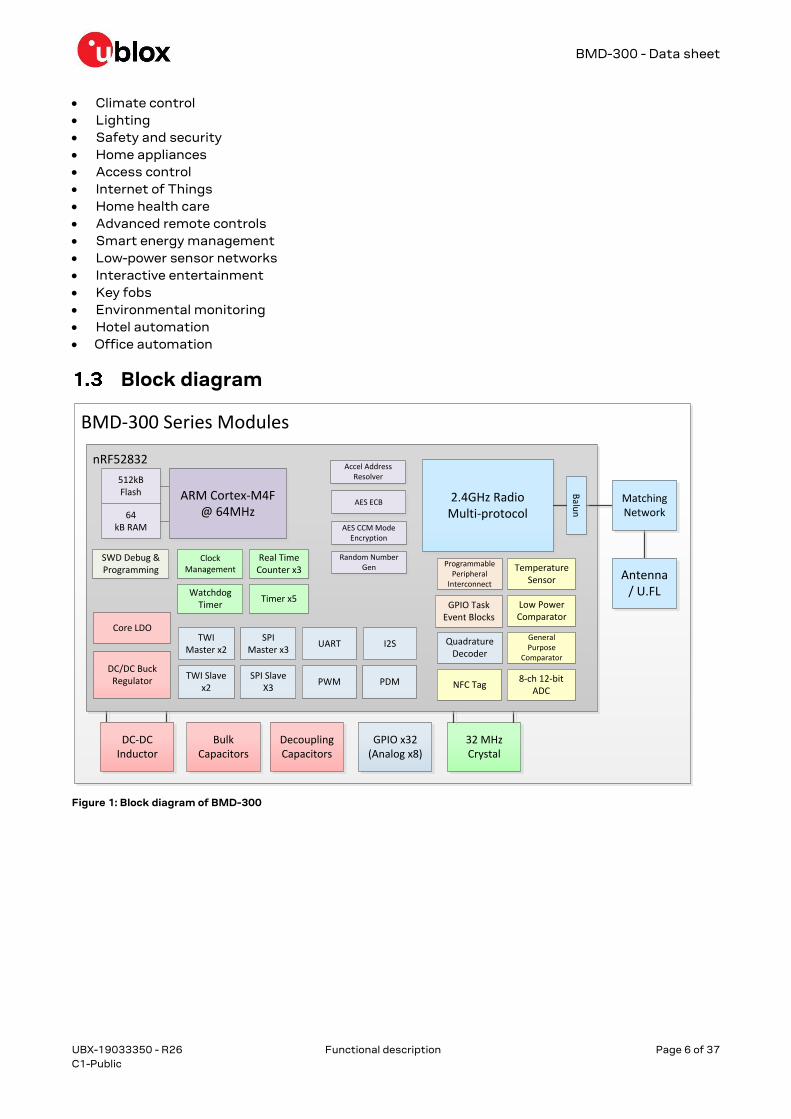
Block diagram
BMD-300 Series Modules
32 MHz Crystal
nRF52832
512kB Flash
DC-DC Inductor
Decoupling Capacitors
Bulk Capacitors
2.4GHz RadioMulti-protocol
TWI Master x2
SPI Master x3
SPI SlaveX3
DC/DC Buck Regulator
Core LDO
64kB RAM
Low Power Comparator
8-ch 12-bit ADC
UART Quadrature Decoder
SWD Debug & Programming Temperature
Sensor
Clock Management
Watchdog Timer
Random Number Gen
Timer x5
Accel Address Resolver
AES CCM Mode Encryption
AES ECB
Real Time Counter x3
GPIO Task Event Blocks
Programmable Peripheral
Interconnect
ARM Cortex-M4F@ 64MHz
Matching Network
Antenna / U.FL
GPIO x32(Analog x8)
I2S
TWI Slave x2
PWM PDM
General Purpose
Comparator
NFC Tag
Balu
n
Figure 1: Block diagram of BMD-300
BMD-300 - Data sheet
UBX-19033350 - R26 Functional description Page 7 of 37
C1-Public
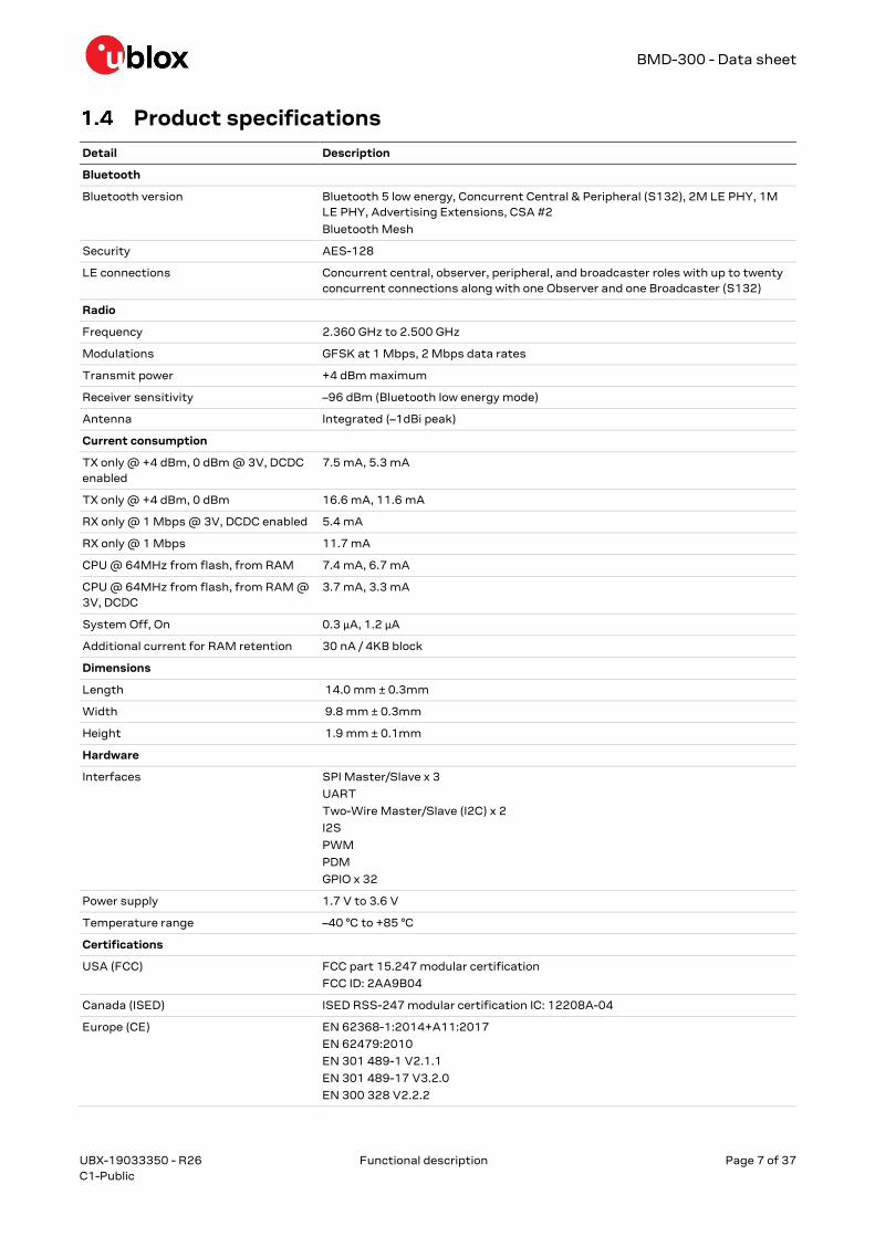
Product specifications
Detail Description
Bluetooth
Bluetooth version Bluetooth 5 low energy, Concurrent Central & Peripheral (S132), 2M LE PHY, 1M
LE PHY, Advertising Extensions, CSA #2
Bluetooth Mesh
Security AES-128
LE connections Concurrent central, observer, peripheral, and broadcaster roles with up to twenty
concurrent connections along with one Observer and one Broadcaster (S132)
Radio
Frequency 2.360 GHz to 2.500 GHz
Modulations GFSK at 1 Mbps, 2 Mbps data rates
Transmit power +4 dBm maximum
Receiver sensitivity –96 dBm (Bluetooth low energy mode)
Antenna Integrated (–1dBi peak)
Current consumption
TX only @ +4 dBm, 0 dBm @ 3V, DCDC
enabled
7.5 mA, 5.3 mA
TX only @ +4 dBm, 0 dBm 16.6 mA, 11.6 mA
RX only @ 1 Mbps @ 3V, DCDC enabled 5.4 mA
RX only @ 1 Mbps 11.7 mA
CPU @ 64MHz from flash, from RAM 7.4 mA, 6.7 mA
CPU @ 64MHz from flash, from RAM @
3V, DCDC
3.7 mA, 3.3 mA
System Off, On 0.3 µA, 1.2 µA
Additional current for RAM retention 30 nA / 4KB block
Dimensions
Length 14.0 mm ± 0.3mm
Width 9.8 mm ± 0.3mm
Height 1.9 mm ± 0.1mm
Hardware
Interfaces SPI Master/Slave x 3
UART
Two-Wire Master/Slave (I2C) x 2
I2S
PWM
PDM
GPIO x 32
Power supply 1.7 V to 3.6 V
Temperature range –40 °C to +85 °C
Certifications
USA (FCC)
FCC part 15.247 modular certification
FCC ID: 2AA9B04
Canada (ISED) ISED RSS-247 modular certification IC: 12208A-04
Europe (CE) EN 62368-1:2014+A11:2017
EN 62479:2010
EN 301 489-1 V2.1.1
EN 301 489-17 V3.2.0
EN 300 328 V2.2.2
BMD-300 - Data sheet
UBX-19033350 - R26 Functional description Page 8 of 37
C1-Public
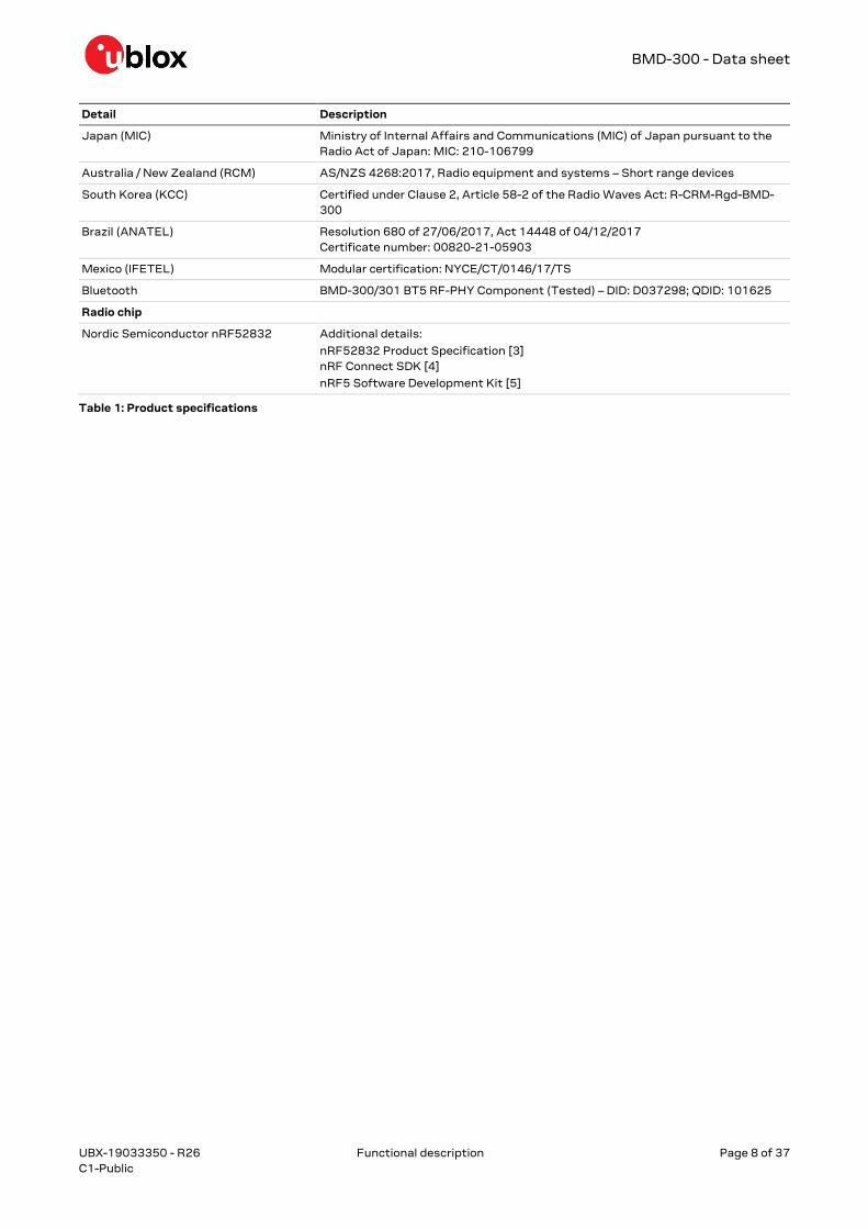
Detail Description
Japan (MIC) Ministry of Internal Affairs and Communications (MIC) of Japan pursuant to the
Radio Act of Japan: MIC: 210-106799
Australia / New Zealand (RCM) AS/NZS 4268:2017, Radio equipment and systems – Short range devices
South Korea (KCC) Certified under Clause 2, Article 58-2 of the Radio Waves Act: R-CRM-Rgd-BMD-
300
Brazil (ANATEL) Resolution 680 of 27/06/2017, Act 14448 of 04/12/2017
Certificate number: 00820-21-05903
Mexico (IFETEL) Modular certification: NYCE/CT/0146/17/TS
Bluetooth BMD-300/301 BT5 RF-PHY Component (Tested) – DID: D037298; QDID: 101625
Radio chip
Nordic Semiconductor nRF52832 Additional details:
nRF52832 Product Specification [3]
nRF Connect SDK [4]
nRF5 Software Development Kit [5]
Table 1: Product specifications
BMD-300 - Data sheet
UBX-19033350 - R26 Pin definition Page 9 of 37
C1-Public
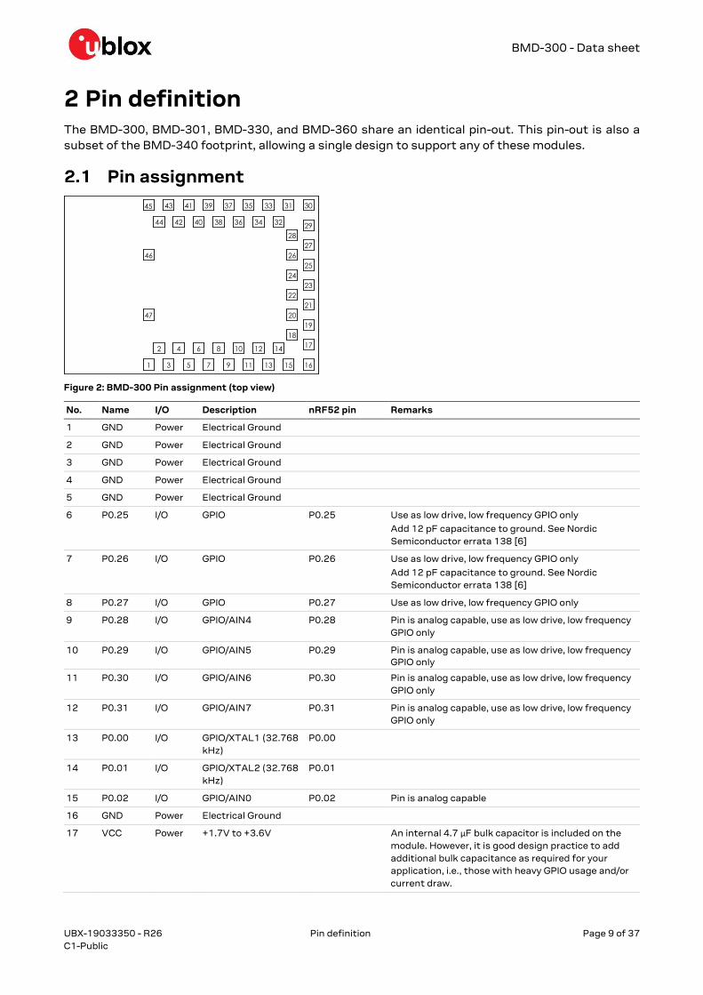
2 Pin definition The BMD-300, BMD-301, BMD-330, and BMD-360 share an identical pin-out. This pin-out is also a
subset of the BMD-340 footprint, allowing a single design to support any of these modules.
Pin assignment
Figure 2: BMD-300 Pin assignment (top view)
No. Name I/O Description nRF52 pin Remarks
1 GND Power Electrical Ground
2 GND Power Electrical Ground
3 GND Power Electrical Ground
4 GND Power Electrical Ground
5 GND Power Electrical Ground
6 P0.25 I/O GPIO P0.25 Use as low drive, low frequency GPIO only
Add 12 pF capacitance to ground. See Nordic
Semiconductor errata 138 [6]
7 P0.26 I/O GPIO P0.26 Use as low drive, low frequency GPIO only
Add 12 pF capacitance to ground. See Nordic
Semiconductor errata 138 [6]
8 P0.27 I/O GPIO P0.27 Use as low drive, low frequency GPIO only
9 P0.28 I/O GPIO/AIN4 P0.28 Pin is analog capable, use as low drive, low frequency
GPIO only
10 P0.29 I/O GPIO/AIN5 P0.29 Pin is analog capable, use as low drive, low frequency
GPIO only 11 P0.30 I/O GPIO/AIN6 P0.30 Pin is analog capable, use as low drive, low frequency
GPIO only
12 P0.31 I/O GPIO/AIN7 P0.31 Pin is analog capable, use as low drive, low frequency
GPIO only
13 P0.00 I/O GPIO/XTAL1 (32.768
kHz)
P0.00
14 P0.01 I/O GPIO/XTAL2 (32.768
kHz)
P0.01
15 P0.02 I/O GPIO/AIN0 P0.02 Pin is analog capable
16 GND Power Electrical Ground
17 VCC Power +1.7V to +3.6V An internal 4.7 µF bulk capacitor is included on the
module. However, it is good design practice to add
additional bulk capacitance as required for your
application, i.e., those with heavy GPIO usage and/or
current draw.
BMD-300 - Data sheet
UBX-19033350 - R26 Pin definition Page 10 of 37
C1-Public
No. Name I/O Description nRF52 pin Remarks
18 GND Power Electrical Ground
19 P0.03 I/O GPIO/AIN1 P0.03 Pin is analog capable
20 P0.04 I/O GPIO/AIN2 P0.04 Pin is analog capable
21 P0.05 I/O GPIO/AIN3 P0.05 Pin is analog capable
22 P0.06 I/O GPIO P0.06
23 P0.07 I/O GPIO P0.07
24 P0.08 I/O GPIO P0.08
25 P0.09 I/O GPIO/NFC1 P0.09 NFC pin 1 (default)
26 P0.10 I/O GPIO/NFC2 P0.10 NFC pin 2 (default)
27 P0.11 I/O GPIO P0.11
28 P0.12 I/O GPIO P0.12
29 GND Power Electrical Ground
30 GND Power Electrical Ground
31 P0.13 I/O GPIO P0.13
32 P0.14 I/O GPIO/TRACEDATA[3] P0.14
33 P0.15 I/O GPIO/TRACEDATA[2] P0.15
34 P0.16 I/O GPIO/TRACEDATA[1] P0.16
35 P0.17 I/O GPIO P0.17
36 P0.18 I/O GPIO/TRACEDATA[0]
/SWO
P0.18
37 P0.19 I/O GPIO P0.19
38 P0.20 I/O GPIO/TRACECLK P0.20
39 P0.21 I/O GPIO/RESET_N P0.21 May be used as active low reset input
40 P0.22 I/O GPIO P0.22 Use as low drive, low frequency GPIO only
41 P0.23 I/O GPIO P0.23 Use as low drive, low frequency GPIO only
42 P0.24 I/O GPIO P0.24 Use as low drive, low frequency GPIO only
43 SWCLK I SWD Clock SWCLK
44 SWDIO I/O SWD IO SWDIO
45 GND Power Electrical Ground
46 GND Power Electrical Ground
47 GND Power Electrical Ground
Table 2: BMD-300 pin-out
Peripheral pin assignments
The peripherals within the BMD-300 may be assigned to nearly any of the GPIO pins through the
application. There are some restrictions called out by the nRF52832 product specification. See the
Remarks in Error! Reference source not found.. Also note that certain peripherals are assigned to
particular pins, such the analog inputs.
Only one peripheral signal can be multiplexed to a GPIO pin at a time. Trace signals, analog inputs,
XTAL signals, SWD interface, and reset are restricted to certain pins due to additional internal
circuitry required by the interface. See Table 3.
Peripheral Signal Pin options
UART0, I2C0, SPI0, SPI1, PDM, PWM0 All P0.00-P0.31
ADC, COMP, LPCOMP All P0.02-P0.05, P0.28-P0.31 (AIN0-AIN7)
Reset RESET_N P0.21
BMD-300 - Data sheet
UBX-19033350 - R26 Pin definition Page 11 of 37
C1-Public
Peripheral Signal Pin options
SWD SWD Clock
SWD IO
SWCLK
SWDIO
32.768 kHz Crystal XTAL1
XTAL2
P0.00
P0.01
Table 3: Peripheral pin options
BMD-300 - Data sheet
UBX-19033350 - R26 Electrical specifications Page 12 of 37
C1-Public
3 Electrical specifications
Stressing the device above one or more of the ratings listed in the Absolute maximum ratings can
cause permanent damage. These are stress ratings only. Operating the module at these or at any
conditions other than those specified in the Operating conditions should be avoided. Exposure to
absolute maximum rating conditions for extended periods can affect device reliability.
Operating condition ranges define those limits within which the functionality of the device is
guaranteed. Where application information is given, it is advisory only and does not form part of
the specification.
Absolute maximum ratings
Symbol Description Min Max Unit
VCC_MAX Voltage on supply pin –0.3 3.9 V
VIO_MAX Voltage on GPIO pins (VCC > 3.6 V) –0.3 3.9 V
VIO_MAX Voltage on GPIO pins (VCC ≤ 3.6V) –0.3 VCC+0.3 V V
TS Storage Temperature Range –40 125 °C
Table 4: Absolute maximum ratings
The product is not protected against overvoltage or reversed voltages. If necessary, voltage spikes
exceeding the power supply voltage specification, given in table above, must be limited to values
within the specified boundaries by using appropriate protection devices.
Operating conditions
Unless otherwise specified, all operating condition specifications are at an ambient temperature
of 25 °C and a supply voltage of 3.0 V.
Operation beyond the specified operating conditions is not recommended and extended exposure
beyond them may affect device reliability.
Symbol Parameter Min Typ. Max Unit
VCC Operating supply voltage 1.7 3.0 3.6 V
TR_VCC Supply rise time (0 V to 1.7 V) - - 60 ms
TA Operating ambient temperature range –40 25 85 ° C
Table 5: Operating conditions
General purpose I/O
The general purpose I/O is organized as one port enabling access and control of the 32 available GPIO
pins via one port, P0. Each GPIO can be accessed with the following user configurable features:
• Input/output direction
• Output drive strength
• Internal pull-up and pull-down resistors
• Wake-up from high- or low-level triggers on all pins
• Trigger interrupt on all pins
• All pins can be used by the PPI task/event system; the maximum number of pins that can be
interfaced through the PPI at the same time is limited by the number of GPIOTE channels
• All pins can be individually configured to carry serial interface or quadrature demodulator signals

BMD-300 - Data sheet
UBX-19033350 - R26 Electrical specifications Page 13 of 37
C1-Public
Symbol Parameter Min Typ. Max Unit
VIH Input high voltage 0.7 x VCC - VCC V
VIL Input low voltage VSS - 0.3 x VCC V
VOH Output high voltage VCC – 0.4 - VCC V
VOL Output low voltage VSS - VSS +0.4 V
RPU Pull-up resistance 11 13 16 kΩ
RPD Pull-down resistance 11 13 16 kΩ
Table 6: GPIO
3.4 Peripheral pin assignments
The peripherals within the BMD-300 may be assigned to nearly any of the GPIO pins through the
application. There are some restrictions called out by the nRF52832 product specification. See the
remarks column of Table 2. Also note that certain peripherals are assigned to particular pins, such
the analog inputs and NFC antenna.
Module reset
GPIO pin P0.21 may be used for a hardware reset. In order to utilize P0.21 as a hardware reset, the
UICR registers PSELRESET[0] and PSELRESET[1] must be set alike, to the value of 0x7FFFFF15.
When P0.21 is programmed as RESET, the internal pull-up is automatically enabled. Nordic
Semiconductor example applications and development kits program P0.21 as RESET_N.
Debug and programming
The BMD-300 supports the two pin Serial Wire Debug (SWD) interface and offers flexible and powerful
mechanism for non-intrusive debugging of program code. Breakpoints, single stepping, and
instruction trace capture of code execution flow are part of this support.
The BMD-300 also supports ETM and ITM trace. Trace data from the ETM and the ITM is sent to an
external debugger via a 4-bit wide parallel trace port. In addition to parallel trace, the TPIU supports
serial trace via the Serial Wire Output (SWO) trace protocol.
Clocks
The BMD-300 requires two clocks, a high frequency clock and a low frequency clock.
The high frequency clock is provided on-module by a high-accuracy 32 MHz crystal as required by the
nRF52832 for radio operation.
The low frequency clock can be provided internally by an RC oscillator or synthesized from the fast
clock, or externally by a 32.768 kHz crystal. An external crystal provides the lowest power
consumption and greatest accuracy. Using the internal RC oscillator with calibration provides
acceptable performance for Bluetooth low energy applications at a reduced cost and slight increase
in power consumption.
The ANT protocol requires the use of an external crystal.
BMD-300 - Data sheet
UBX-19033350 - R26 Electrical specifications Page 14 of 37
C1-Public
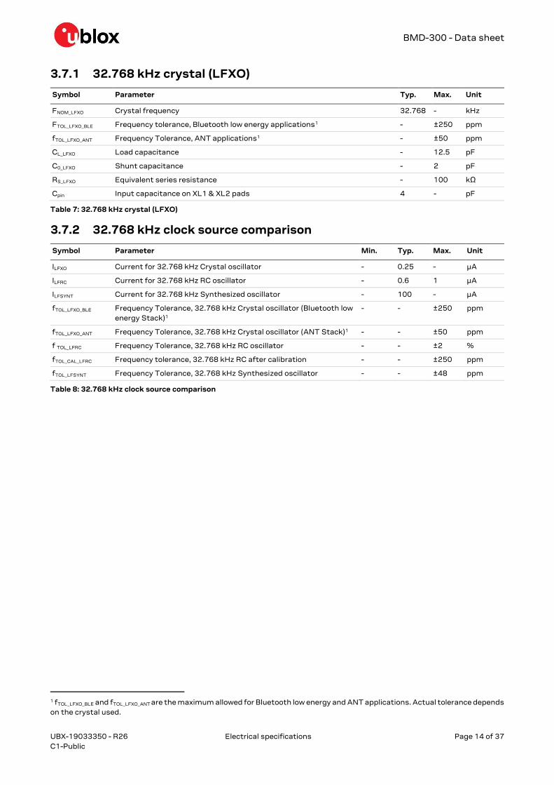
3.7.1 32.768 kHz crystal (LFXO)
Symbol Parameter Typ. Max. Unit
FNOM_LFXO Crystal frequency 32.768 - kHz
FTOL_LFXO_BLE Frequency tolerance, Bluetooth low energy applications1 - ±250 ppm
fTOL_LFXO_ANT Frequency Tolerance, ANT applications1 - ±50 ppm
CL_LFXO Load capacitance - 12.5 pF
C0_LFXO Shunt capacitance - 2 pF
RS_LFXO Equivalent series resistance - 100 kΩ
Cpin Input capacitance on XL1 & XL2 pads 4 - pF
Table 7: 32.768 kHz crystal (LFXO)
3.7.2 32.768 kHz clock source comparison
Symbol Parameter Min. Typ. Max. Unit
ILFXO Current for 32.768 kHz Crystal oscillator - 0.25 - µA
ILFRC Current for 32.768 kHz RC oscillator - 0.6 1 µA
ILFSYNT Current for 32.768 kHz Synthesized oscillator - 100 - µA
fTOL_LFXO_BLE Frequency Tolerance, 32.768 kHz Crystal oscillator (Bluetooth low
energy Stack)1
- - ±250 ppm
fTOL_LFXO_ANT Frequency Tolerance, 32.768 kHz Crystal oscillator (ANT Stack)1 - - ±50 ppm
f TOL_LFRC Frequency Tolerance, 32.768 kHz RC oscillator - - ±2 %
fTOL_CAL_LFRC Frequency tolerance, 32.768 kHz RC after calibration - - ±250 ppm
fTOL_LFSYNT Frequency Tolerance, 32.768 kHz Synthesized oscillator - - ±48 ppm
Table 8: 32.768 kHz clock source comparison
1 fTOL_LFXO_BLE and fTOL_LFXO_ANT are the maximum allowed for Bluetooth low energy and ANT applications. Actual tolerance depends
on the crystal used.

BMD-300 - Data sheet
UBX-19033350 - R26 Firmware Page 15 of 37
C1-Public
4 Firmware Projects for the BMD-360 should utilize the Nordic Semiconductor nRF Connect SDK [4] and the
nRF52832 tools for new development. The tools allow access to the very latest Bluetooth support
from Nordic Semiconductor and provide an ongoing path as new features are released.
The nRF5 SDK Error! Reference source not found. can also be used if the feature set of the SDK meets
the application requirements.
For legacy applications, source code is provided through our GitHub repositories for RigDFU,
BMDware, Rigablue, developer tools, and mobile apps for customers to customize and extend on
their own.
Factory image
The factory programmed firmware version is indicated on the label. Programming of the factory image
is maintained solely for legacy applications. New development should use the latest Nordic
Semiconductor SDK and examples.
4.1.1 Firmware version “AA”
• RigDFU v3.2.0 (42)
• Nordic Semiconductor S132 SoftDevice v2.0.0
• BMDware v3.1.0 (50)
• Read-back protection enabled.
Modules can be programmed with customer code after a full-chip erase via the SWD interface.
A full-chip erase will clear the assigned public Bluetooth device (MAC) address from memory. With
Firmware Version AA and AB, the MAC address must be manually recovered.
4.1.2 Firmware version “AB”
• RigDFU v3.2.1 (43)
• Nordic Semiconductor S132 SoftDevice v2.0.0
• BMDware v3.1.1 (51)
• Read-back protection enabled.
Modules can be programmed with customer code after a full-chip erase via the SWD interface.
A full-chip erase will clear the assigned public Bluetooth device (MAC) address from memory. With
Firmware Version AA and AB, the MAC address must be manually recovered.
4.1.3 Firmware version “AC”
• RigDFU v3.2.2 (44)
• Nordic Semiconductor S132 SoftDevice v2.0.0
• BMDware v3.1.1 (51)
• Read-back protection disabled.
Modules can be programmed with customer code after a full-chip erase via the SWD interface.
A full chip erase clears the assigned public Bluetooth device (MAC) address from memory. See also
Bluetooth device address.
BMD-300 - Data sheet
UBX-19033350 - R26 Firmware Page 16 of 37
C1-Public
4.1.4 Firmware version “AD”
• RigDFU v3.3.1 (46)
• Nordic Semiconductor S132 SoftDevice v3.1.0
• BMDware v3.2.1 (60)
• Read-back protection disabled.
Modules can be programmed with customer code after a full-chip erase via the SWD interface.
A full chip erase clears the assigned public Bluetooth device (MAC) address from memory. See also
Bluetooth device address.
4.1.5 Firmware version “AE”
• RigDFU v3.4.0 (47)
• Nordic Semiconductor S132 SoftDevice v3.1.0
• BMDware v3.2.1 (60)
• Read-back protection disabled.
Modules can be programmed with customer code after a full-chip erase via the SWD interface.
A full chip erase will clear the assigned public Bluetooth device (MAC) address from memory. See
also Bluetooth device address.
“AE” marked modules may not be loaded with previous factory firmware versions due to Nordic
Semiconductor nRF52832 Errata #108. “AA” through “AD” marked modules may be loaded with
any Factory Firmware version, including “AE”.
Type numbers BMD-300-A-R-10 and BMD-300-A-R-20 are loaded with firmware version “AE” only.
Module programming and read-back protection
For legacy applications, RigDFU allows for UART and OTA updates to RigDFU, the SoftDevice and
application firmware.
In order to utilize the SWD port on “AA” and “AB” marked modules, the nRF52832 must be erased and
recovered. Without this step, the module will not be recognized by most programmers. This is
accomplished through nrfjprog, which is provided with the Nordic Semiconductor command line
utilities:
nrfjprog -f nrf52 ––recover
A full chip erase is performed, so all components will need to be re-loaded (bootloader, SoftDevice,
application firmware, and if used the public Bluetooth device address).
The BMD-300 module may be restored to the factory firmware versions noted above with the utilities
available at our GitHub repositories.
SoftDevices
Nordic Semiconductor protocol stacks are known as SoftDevices. SoftDevices are pre-compiled, pre-
linked binary files. SoftDevices can be programmed in nRF52 series SoCs and are downloadable from
the Nordic Semiconductor website. The BMD-300 with the nRF52832 SoC supports the S132
(Bluetooth low energy Central & Peripheral), S212 (ANT) and S312 (ANT and Bluetooth low energy)
SoftDevices.

BMD-300 - Data sheet
UBX-19033350 - R26 Firmware Page 17 of 37
C1-Public
4.3.1 S132
The S132 SoftDevice is a Bluetooth® low energy Central and Peripheral protocol stack solution
supporting up to twenty connections with an additional Observer and a Broadcaster role all running
concurrently. The S132 SoftDevice integrates a Bluetooth low energy Controller and Host and
provides a full and flexible API for building Bluetooth Smart nRF52 System on Chip (SoC) solutions.
4.3.2 S212
The S212 SoftDevice is an ANT™ protocol stack solution that provides a full and flexible Application
Programming Interface (API) for building ANT System on Chip (SoC) solutions for the nRF52832 chip.
The S212 SoftDevice simplifies combining the ANT protocol stack and an application on the same
CPU. See the ANT+ website for membership in the ANT+ Alliance and S212 licensing.
4.3.3 S332
The S332 SoftDevice is a combined ANT and Bluetooth low energy protocol stack solution. It supports
all four Bluetooth low energy roles (central, peripheral, observer, broadcaster) and ANT.
The S332 SoftDevice provides a full and flexible Application Programming Interface (API) for building
concurrent ANT and Bluetooth low energy System on Chip (SoC) solutions. It simplifies combining an
ANT and Bluetooth low energy protocol stack and an application on the same CPU, therefore
eliminating the need for an added device to support concurrent multiprotocol. See the ANT+ website
for membership in the ANT+ Alliance and S332 licensing.
Bluetooth device address
The BMD-300 module is preprogrammed from the factory with a unique public Bluetooth device
(MAC) address stored in the CUSTOMER[0] and CUSTOMER[1] registers of the User Information
Configuration Registers (UICR). The Bluetooth device address consists of the IEEE Organizationally
Unique Identifier (OUI) combined with the six hexadecimal digits that are printed on a 2D barcode and
in human-readable text on the module label, as described in Module marking. The Bluetooth device
address is stored in little endian format. The most significant bytes of the CUSTOMER[1] register are
0xFF to complete the 32-bit register.
UICR Register Address Description Remarks
CUSTOMER[0] 0x10001080 Bluetooth_addr [0] (0xFF) Example value. Actual value printed on label
CUSTOMER[0] 0x10001081 Bluetooth_addr [1] (0xEE) Example value. Actual value printed on label
CUSTOMER[0] 0x10001082 Bluetooth_addr [2] (0xDD) Example value. Actual value printed on label
CUSTOMER[0] 0x10001083 Bluetooth_addr [3] (0xCC) IEEE OUI2,3
CUSTOMER[1] 0x10001084 Bluetooth_addr [4] (0xBB) IEEE OUI2,3
CUSTOMER[1] 0x10001085 Bluetooth_addr [5] (0xAA) IEEE OUI2,3
CUSTOMER[1] 0x10001086 0xFF Unused
CUSTOMER[1] 0x10001087 0xFF Unused
Table 9: Bluetooth device address
2 The IEEE OUI for type number BMD-300-A-R-00 is: 94:54:93. The second half of the full Bluetooth device address is encoded
in the label data matrix. The full Bluetooth device address is stored in the UICR. 3 Type numbers BMD-300-A-R-10 and BMD-300-A-R-20 encode the full Bluetooth device address in the label data matrix and
is stored in the UICR.

BMD-300 - Data sheet
UBX-19033350 - R26 Mechanical specifications Page 18 of 37
C1-Public
5 Mechanical specifications
Dimensions
Length: ± 0.3 mm, Width: ± 0.3 mm, Height: ± 0.1 mm
Figure 3: BMD-300 mechanical drawing
Recommended PCB land pads
Figure 4: Recommended PCB Land Pads
The RF Keep-out area extends vertically to the board edge.
BMD-300 - Data sheet
UBX-19033350 - R26 Mechanical specifications Page 19 of 37
C1-Public
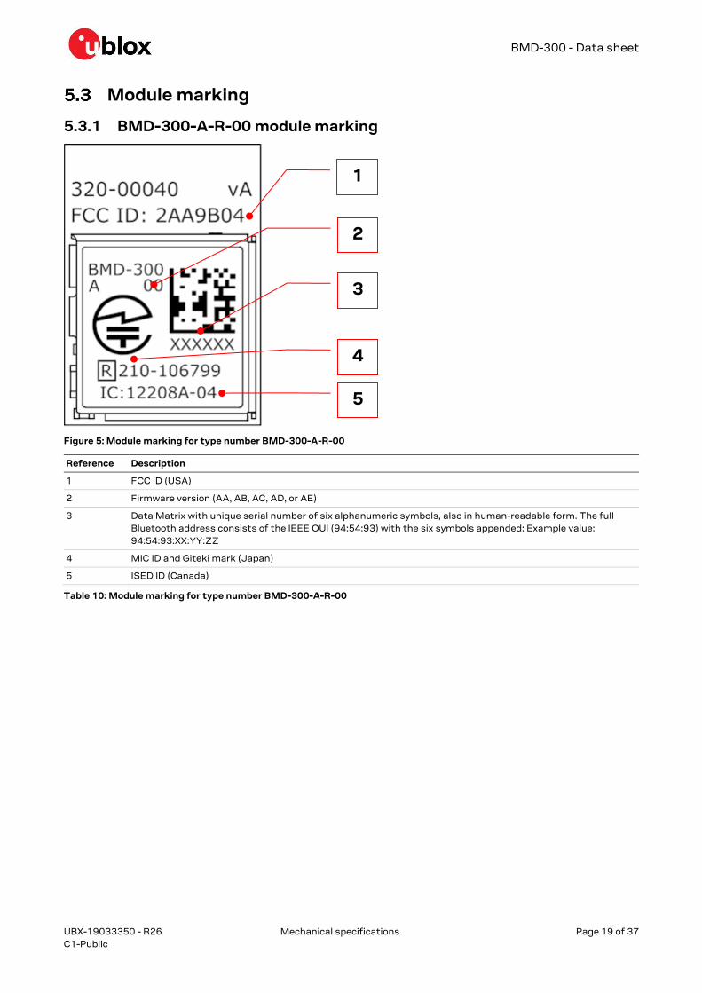
Module marking
5.3.1 BMD-300-A-R-00 module marking
Figure 5: Module marking for type number BMD-300-A-R-00
Reference Description
1 FCC ID (USA)
2 Firmware version (AA, AB, AC, AD, or AE)
3 Data Matrix with unique serial number of six alphanumeric symbols, also in human-readable form. The full
Bluetooth address consists of the IEEE OUI (94:54:93) with the six symbols appended: Example value:
94:54:93:XX:YY:ZZ
4 MIC ID and Giteki mark (Japan)
5 ISED ID (Canada)
Table 10: Module marking for type number BMD-300-A-R-00
3
2
1
4
5
BMD-300 - Data sheet
UBX-19033350 - R26 Mechanical specifications Page 20 of 37
C1-Public
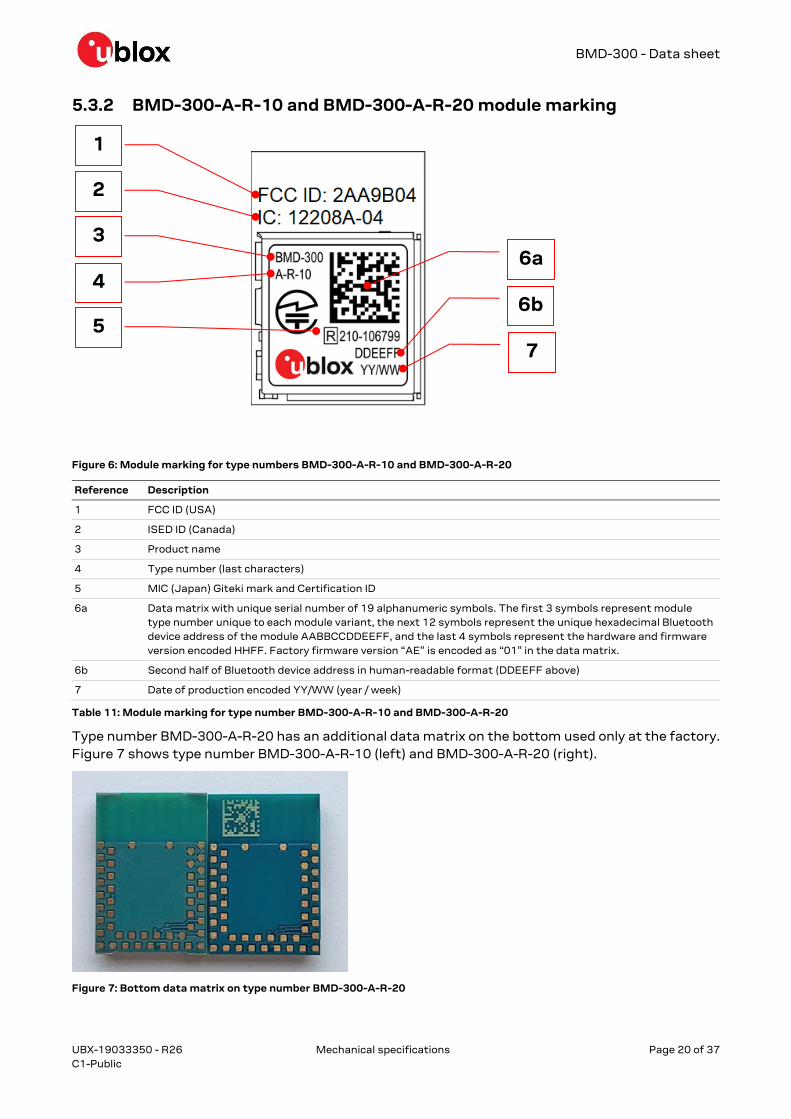
5.3.2 BMD-300-A-R-10 and BMD-300-A-R-20 module marking
Figure 6: Module marking for type numbers BMD-300-A-R-10 and BMD-300-A-R-20
Reference Description
1 FCC ID (USA)
2 ISED ID (Canada)
3 Product name
4 Type number (last characters)
5 MIC (Japan) Giteki mark and Certification ID
6a Data matrix with unique serial number of 19 alphanumeric symbols. The first 3 symbols represent module
type number unique to each module variant, the next 12 symbols represent the unique hexadecimal Bluetooth
device address of the module AABBCCDDEEFF, and the last 4 symbols represent the hardware and firmware
version encoded HHFF. Factory firmware version “AE” is encoded as “01” in the data matrix.
6b Second half of Bluetooth device address in human-readable format (DDEEFF above)
7 Date of production encoded YY/WW (year / week)
Table 11: Module marking for type number BMD-300-A-R-10 and BMD-300-A-R-20
Type number BMD-300-A-R-20 has an additional data matrix on the bottom used only at the factory.
Figure 7 shows type number BMD-300-A-R-10 (left) and BMD-300-A-R-20 (right).
Figure 7: Bottom data matrix on type number BMD-300-A-R-20
1
2
3
4
5
6a
6b
7
BMD-300 - Data sheet
UBX-19033350 - R26 RF design notes Page 21 of 37
C1-Public
6 RF design notes
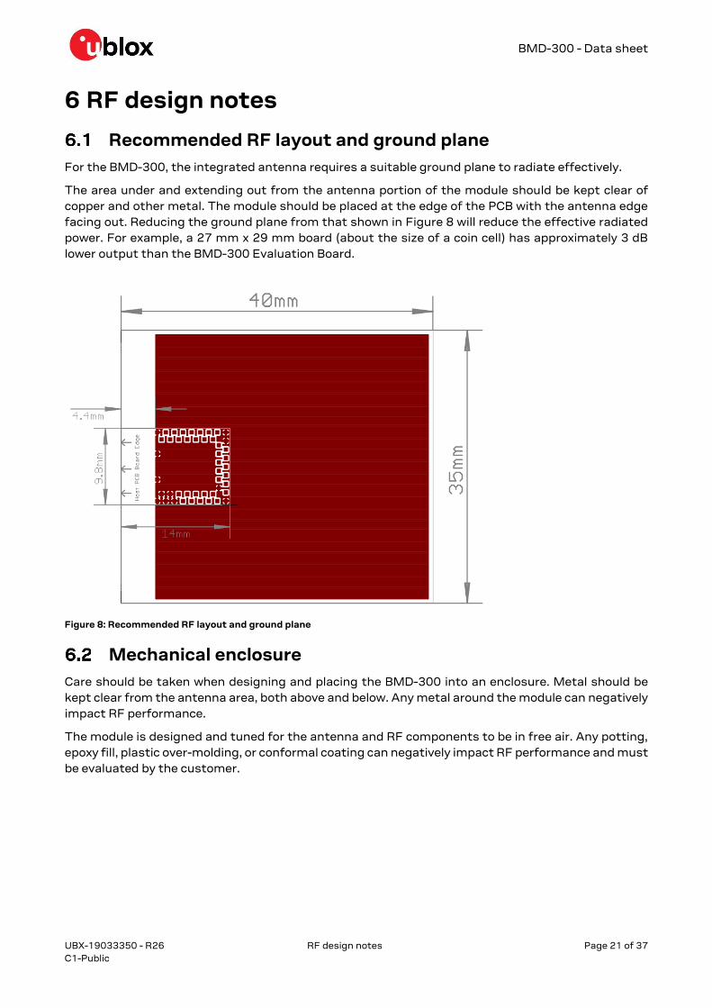
Recommended RF layout and ground plane
For the BMD-300, the integrated antenna requires a suitable ground plane to radiate effectively.
The area under and extending out from the antenna portion of the module should be kept clear of
copper and other metal. The module should be placed at the edge of the PCB with the antenna edge
facing out. Reducing the ground plane from that shown in Figure 8 will reduce the effective radiated
power. For example, a 27 mm x 29 mm board (about the size of a coin cell) has approximately 3 dB
lower output than the BMD-300 Evaluation Board.
Figure 8: Recommended RF layout and ground plane
Mechanical enclosure
Care should be taken when designing and placing the BMD-300 into an enclosure. Metal should be
kept clear from the antenna area, both above and below. Any metal around the module can negatively
impact RF performance.
The module is designed and tuned for the antenna and RF components to be in free air. Any potting,
epoxy fill, plastic over-molding, or conformal coating can negatively impact RF performance and must
be evaluated by the customer.
BMD-300 - Data sheet
UBX-19033350 - R26 RF design notes Page 22 of 37
C1-Public
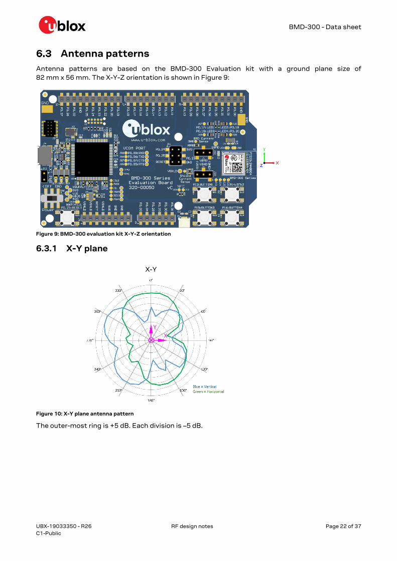
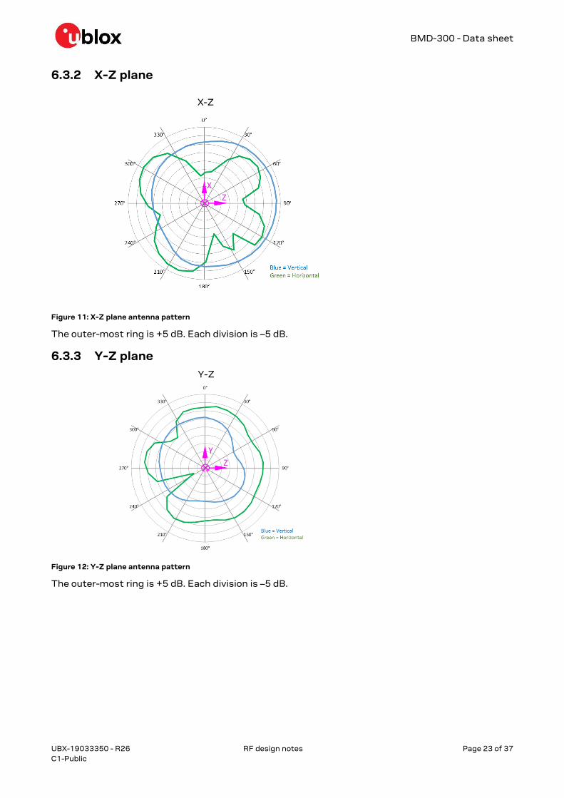
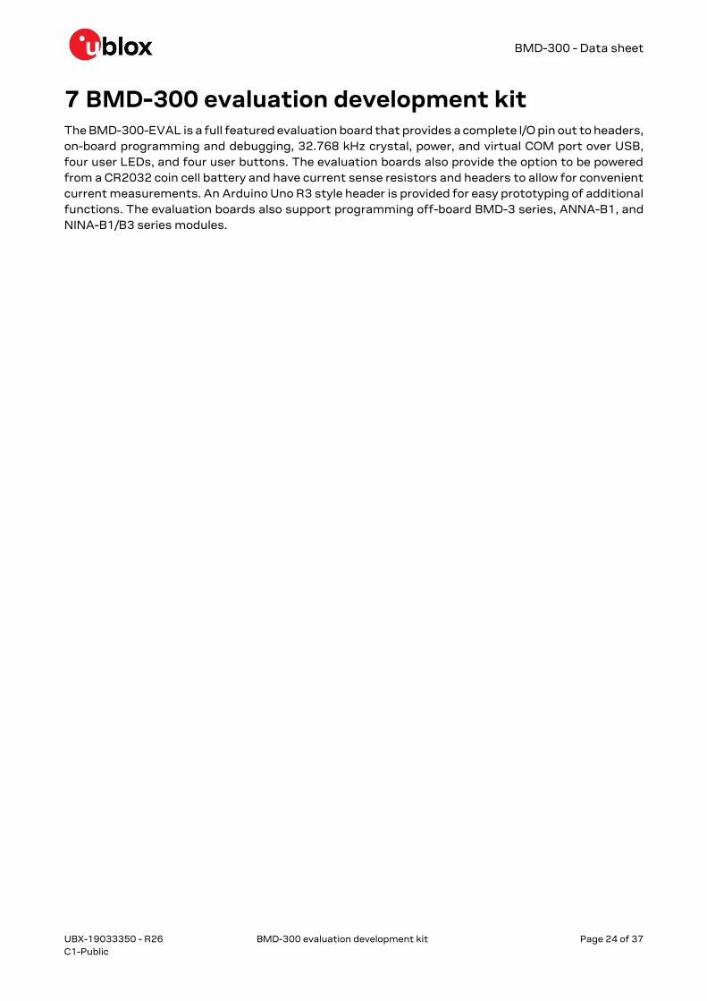
Antenna patterns
Antenna patterns are based on the BMD-300 Evaluation kit with a ground plane size of
82 mm x 56 mm. The X-Y-Z orientation is shown in Figure 9:
Figure 9: BMD-300 evaluation kit X-Y-Z orientation
6.3.1 X-Y plane
Figure 10: X-Y plane antenna pattern
The outer-most ring is +5 dB. Each division is –5 dB.
X-Y
Y
X
BMD-300 - Data sheet
UBX-19033350 - R26 RF design notes Page 23 of 37
C1-Public
6.3.2 X-Z plane
Figure 11: X-Z plane antenna pattern
The outer-most ring is +5 dB. Each division is –5 dB.
6.3.3 Y-Z plane
Figure 12: Y-Z plane antenna pattern
The outer-most ring is +5 dB. Each division is –5 dB.
Y
Z
X
Z
X-Z
Y-Z
BMD-300 - Data sheet
UBX-19033350 - R26 BMD-300 evaluation development kit Page 24 of 37
C1-Public
7 BMD-300 evaluation development kit The BMD-300-EVAL is a full featured evaluation board that provides a complete I/O pin out to headers,
on-board programming and debugging, 32.768 kHz crystal, power, and virtual COM port over USB,
four user LEDs, and four user buttons. The evaluation boards also provide the option to be powered
from a CR2032 coin cell battery and have current sense resistors and headers to allow for convenient
current measurements. An Arduino Uno R3 style header is provided for easy prototyping of additional
functions. The evaluation boards also support programming off-board BMD-3 series, ANNA-B1, and
NINA-B1/B3 series modules.
BMD-300 - Data sheet
UBX-19033350 - R26 Qualification and approvals Page 25 of 37
C1-Public
8 Qualification and approvals
United States (FCC):
The BMD-300 has received Federal Communications Commission (FCC) CFR47 Telecommunications,
Part 15 Subpart C “Intentional Radiators” modular approval in accordance with Part 15.247 Modular
Transmitter approval. The modular approval allows the end user to integrate the module into a
finished product without obtaining subsequent and separate FCC approvals for intentional radiation,
provided no changes or modifications are made to the module circuitry. Changes or modifications
could void the user’s authority to operate the equipment. The end user must comply with all of the
instructions provided by the Grantee, which indicate installation and/or operating conditions
necessary for compliance.
The finished product is required to comply with all applicable FCC equipment authorizations
regulations, requirements and equipment functions not associated with the transmitter module
portion. For example, compliance must be demonstrated to regulations for other transmitter
components within the host product; to requirements for unintentional radiators (Part 15 Subpart B
“Unintentional Radiators”), such as digital devices, computer peripherals, radio receivers, etc.; and to
additional authorization requirements for the non-transmitter functions on the transmitter module
(i.e., Verification, or Declaration of Conformity) (e.g., transmitter modules may also contain digital
logic functions) as appropriate.
Modification to this product will void the users’ authority to operate this equipment.
The OEM is still responsible for verifying end product compliance with FCC Part 15, subpart B
limits for unintentional radiators through an accredited test facility.
8.1.1 Labeling and user information requirements
The BMD-300 is assigned the FCC ID number: 2AA9B04
If the FCC ID is not visible when the module is installed inside another device, then the outside of the
finished product into which the module is installed must also display a label referring to the enclosed
module. This exterior label can use the following or similar wording:
Contains FCC ID: 2AA9B04
In addition to marking the product with the appropriate FCC ID, the end product user manual may also
require specific information based on the digital device classification. Refer to the FCC Rules, Title 47,
Subchapter A, Part 15, Subpart B, Chapter §15.105 for specific wording of the notices.
8.1.2 RF exposure
All transmitters regulated by FCC must comply with RF exposure requirements. KDB 447498 General
RF Exposure Guidance provides guidance in determining whether proposed or existing transmitting
facilities, operations or devices comply with limits for human exposure to Radio Frequency (RF) fields
adopted by the Federal Communications Commission (FCC).
This module is approved for installation into mobile and/or portable host platforms and must not be
co-located or operating in conjunction with any other antenna or transmitter except in accordance
with FCC multi-transmitter guidelines. End users must be provided with transmitter operating
conditions for satisfying RF Exposure compliance.
BMD-300 - Data sheet
UBX-19033350 - R26 Qualification and approvals Page 26 of 37
C1-Public
Canada (ISED)
The BMD-300 module is certified for use in Canada under Innovation, Science and Economic
Development Canada (ISED) Radio Standards Specification (RSS) RSS-247 and RSSGen.
8.2.1 Labeling and user information requirements
The BMD-300 is assigned the IC ID number: 12208A-04
Labeling Requirements for the Host Device (from Section 3.2.1, RSS-Gen, Issue 3, December 2010):
The host device shall be properly labeled to identify the module within the host device. The Industry
Canada certification label of a module shall be clearly visible at all times when installed in the host
device, otherwise the host device must be labeled to display the Industry Canada certification number
of the module, preceded by the words “Contains transmitter module”, or the word “Contains”, or
similar wording expressing the same meaning, as follows:
Contains transmitter module IC: 12208A-04
User Manual Notice for License-Exempt Radio Apparatus (from Section 7.1.3 RSS-Gen, Issue 3,
December 2010): User manuals for license-exempt radio apparatus shall contain the following or
equivalent notice in a conspicuous location in the user manual or alternatively on the device or both:
This device complies with Industry Canada license exempt RSS standard(s). Operation is
subject to the following two conditions: (1) this device may not cause interference, and (2)
this device must accept any interference, including interference that may cause undesired
operation of the device.
Le présent appareil est conforme aux CNR d'Industrie Canada applicables aux appareils radio
exempts de licence. L'exploitation est autorisée aux deux conditions suivantes: (1) l'appareil
ne doit pas produire de brouillage, et (2) l'utilisateur de l'appareil doit accepter tout brouillage
radioélectrique subi, même si le brouillage est susceptible d'en compromettre le
fonctionnement.
Transmitter Antenna (from Section 7.1.2 RSS-Gen, Issue 3, December 2010): User manuals
for transmitters shall display the following notice in a conspicuous location:
Under Industry Canada regulations, this radio transmitter may only operate using an
antenna of a type and maximum (or lesser) gain approved for the transmitter by Industry
Canada. To reduce potential radio interference to other users, the antenna type and its gain
should be so chosen that the equivalent isotropically radiated power (e.i.r.p.) is not more than
that necessary for successful communication.
Conformément à la réglementation d'Industrie Canada, le présent émetteur radio peut
fonctionner avec une antenne d'un type et d'un gain maximal (ou inférieur) approuvé pour
l'émetteur par Industrie Canada. Dans le but de réduire les risques de brouillage
radioélectrique à l'intention des autres utilisateurs, il faut choisir le type d'antenne et son
gain de sorte que la puissance isotrope rayonnée équivalente (p.i.r.e.) ne dépasse pas
l'intensité nécessaire à l'établissement d'une communication satisfaisante.
8.2.2 RF exposure
All transmitters regulated by IC must comply with RF exposure requirements listed in RSS-102 - Radio
Frequency (RF) Exposure Compliance of Radiocommunication Apparatus (All Frequency Bands). This
module is approved for installation into mobile and/or portable host platforms and must not be
co-located or operating in conjunction with any other antenna or transmitter except in accordance
with Industry Canada's multi-transmitter guidelines. End users must be provided with transmitter
operating conditions for satisfying RF Exposure compliance.
BMD-300 - Data sheet
UBX-19033350 - R26 Qualification and approvals Page 27 of 37
C1-Public
European Union regulatory compliance
Information about regulatory compliance of the European Union for the BMD-300 module is available
in the BMD-300 Declaration of Conformity.
8.3.1 Radio Equipment Directive (RED) 2014/53/EU
The BMD-300 module complies with the essential requirements and other relevant provisions of
Radio Equipment Directive (RED) 2014/53/EU.
8.3.2 Labeling and user information requirements
The label on the final products which contain the BMD-300 module must follow CE marking
requirements. The “R&TTE Compliance Association Technical Guidance Note 01” provides guidance
on final product CE marking.
Japan (MIC)
The BMD-300 module has received type certification and is labeled with its own technical conformity
mark and certification number as required to conform to the technical standards regulated by the
Ministry of Internal Affairs and Communications (MIC) of Japan pursuant to the Radio Act of Japan.
Integration of this module into a final end product does not require additional radio certification
provided installation instructions are followed and no modifications of the module are allowed.
Additional testing may be required:
• If the host product is subject to electrical appliance safety (for example, powered from an AC
mains), the host product may require Product Safety Electrical Appliance and Material (PSE)
testing. The integrator should contact their conformance laboratory to determine if this testing is
required.
• There is a voluntary Electromagnetic Compatibility (EMC) test for the host product administered
by VCCI: http://www.vcci.jp/vcci_e/index.html
The label on the end product which contains a BMD-300 Series module must follow the MIC marking
requirements. Labeling requirements for Japan available at the Ministry of Internal Affairs and
Communications (MIC) website: http://www.tele.soumu.go.jp/e/index.htm.
The BMD-300 module is labeled with its assigned technical conformity mark and certification number.
The end product in which this module is being used must have an external label referring to the type
certified module inside:
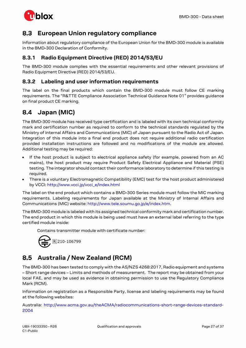
Contains transmitter module with certificate number:
Australia / New Zealand (RCM)
The BMD-300 has been tested to comply with the AS/NZS 4268:2017, Radio equipment and systems
– Short range devices – Limits and methods of measurement. The report may be obtained from your
local FAE, and may be used as evidence in obtaining permission to use the Regulatory Compliance
Mark (RCM).
Information on registration as a Responsible Party, license and labeling requirements may be found
at the following websites:
Australia: http://www.acma.gov.au/theACMA/radiocommunications-short-range-devices-standard-
2004
BMD-300 - Data sheet
UBX-19033350 - R26 Qualification and approvals Page 28 of 37
C1-Public
New Zealand: http://www.rsm.govt.nz/compliance
Only Australian-based and New Zealand-based companies who are registered may be granted
permission to use the RCM. An Australian-based or New Zealand-based agent or importer may also
register as a Responsible Party to use the RCM on behalf of a company not in Australia or New
Zealand.
South Korea (KCC)
The BMD-300 is certified under Clause 2, Article 58-2 of the Radio Waves Act.
When a product containing the BMD-300 is placed on the South Korean market, the product must be
affixed with a label or marking containing the KCC logo and certification number as shown in the
following figure. This information must also be included in the product user manuals.
R-CRM-Rgd-BMD-300
The height of the KCC logo must be at least 5 mm.
Brazil (ANATEL)
The BMD-300 is evaluated according to: Resolution 680 of 27/06/2017, Act 14448 of 04/12/2017,
Certificate number: 00820-21-05903.
The end products that contain these modules must list the ANATEL number from the modular
approval. The number can go on the end product label, manual, box or software, with the following
phrase:
Contains ANATEL approved module # 00820-21-05903
Mexico (IFETEL)
The end products that contain these modules must list the IFETEL number from the modular
approval. The number can go on the end product label, manual, box or software, with the following
phrase:
Este equipo contiene el módulo BMD-300 con Número IFETEL: NYCE/CT/0146/17/TS
- or -
Este equipo contiene el módulo con IFT #: NYCE/CT/0146/17/TS
Bluetooth qualification
The Bluetooth SIG maintains the Bluetooth Specification, and ensures that products are properly
tested and comply with the Bluetooth license agreements. Companies that list products with the
Bluetooth SIG are required to be members of the SIG and submit the listed fees. Refer to this link for
details: https://www.bluetooth.com/develop-with-bluetooth/qualification-listing
The BMD-300 Bluetooth Low Energy module based on the Nordic Semiconductor nRF52832 is listed
as a “Tested Component”, with Qualified Design ID 101625. This allows an end-product based on a
BMD-300 module to inherit the component listings without the need to run through all of the tests
again. The end-product will often inherit several QDIDs, and are identified on a “Declaration of
Compliance”.
The BMD-300 primarily utilizes the S132 SoftDevice.
BMD-300 - Data sheet
UBX-19033350 - R26 Environmental Page 29 of 37
C1-Public
9 Environmental
RoHS
The BMD-300 is in compliance with Directive 2011/65/EU, 2015/863/EU of the European Parliament
and the Council on the restriction of the use of certain hazardous substances in electrical and
electronic equipment. The RoHS declaration is available in the BMD-300 EU Declaration of Conformity
[2].
REACH
The BMD-300 does not contain the SVHC (Substance of Very High Concern), as defined by Directive
EC/1907/2006 Article according to REACH Annex XVII.
California proposition 65 (P65)
This product can expose you to Nickel (metallic), which is known to the State of California to cause
cancer. For more information go to www.P65Warnings.ca.gov. Warnings are not required where the
listed chemical is inaccessible to the average user of the end product.
BMD-300 - Data sheet
UBX-19033350 - R26 Product handling Page 30 of 37
C1-Public
10 Product handling
Packaging
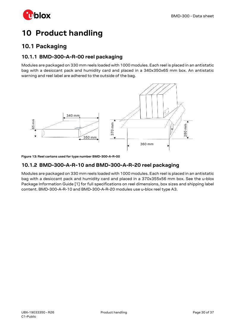
10.1.1 BMD-300-A-R-00 reel packaging
Modules are packaged on 330 mm reels loaded with 1000 modules. Each reel is placed in an antistatic
bag with a desiccant pack and humidity card and placed in a 340x350x65 mm box. An antistatic
warning and reel label are adhered to the outside of the bag.
Figure 13: Reel cartons used for type number BMD-300-A-R-00
10.1.2 BMD-300-A-R-10 and BMD-300-A-R-20 reel packaging
Modules are packaged on 330 mm reels loaded with 1000 modules. Each reel is placed in an antistatic
bag with a desiccant pack and humidity card and placed in a 370x355x56 mm box. See the u-blox
Package Information Guide [1] for full specifications on reel dimensions, box sizes and shipping label
content. BMD-300-A-R-10 and BMD-300-A-R-20 modules use u-blox reel type A3.
BMD-300 - Data sheet
UBX-19033350 - R26 Product handling Page 31 of 37
C1-Public
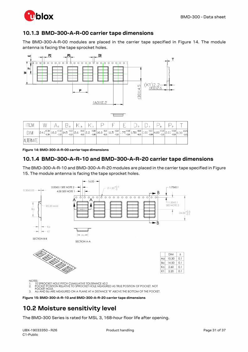
10.1.3 BMD-300-A-R-00 carrier tape dimensions
The BMD-300-A-R-00 modules are placed in the carrier tape specified in Figure 14. The module
antenna is facing the tape sprocket holes.
Figure 14: BMD-300-A-R-00 carrier tape dimensions
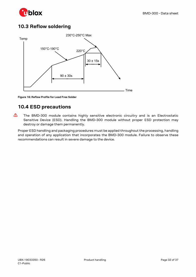
10.1.4 BMD-300-A-R-10 and BMD-300-A-R-20 carrier tape dimensions
The BMD-300-A-R-10 and BMD-300-A-R-20 modules are placed in the carrier tape specified in Figure
15. The module antenna is facing the tape sprocket holes.
Figure 15: BMD-300-A-R-10 and BMD-300-A-R-20 carrier tape dimensions
Moisture sensitivity level
The BMD-300 Series is rated for MSL 3, 168-hour floor life after opening.
BMD-300 - Data sheet
UBX-19033350 - R26 Product handling Page 32 of 37
C1-Public
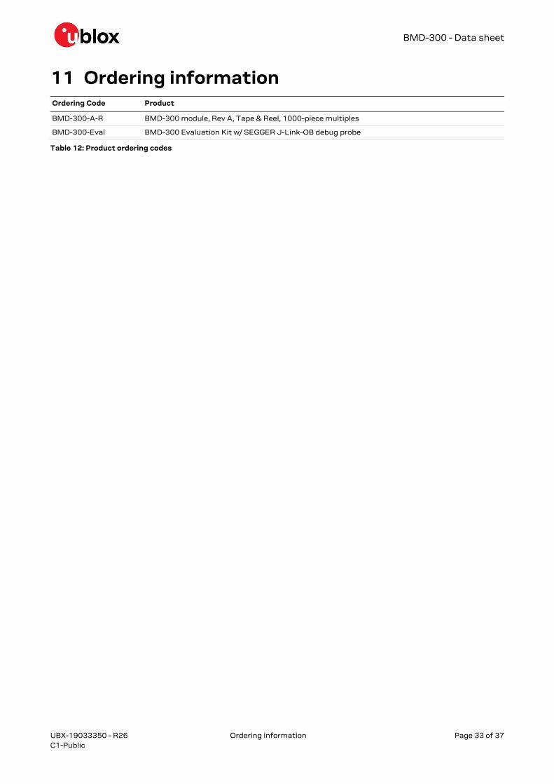
Reflow soldering
Figure 16: Reflow Profile for Lead Free Solder
ESD precautions
The BMD-300 module contains highly sensitive electronic circuitry and is an Electrostatic
Sensitive Device (ESD). Handling the BMD-300 module without proper ESD protection may
destroy or damage them permanently.
Proper ESD handling and packaging procedures must be applied throughout the processing, handling
and operation of any application that incorporates the BMD-300 module. Failure to observe these
recommendations can result in severe damage to the device.
BMD-300 - Data sheet
UBX-19033350 - R26 Ordering information Page 33 of 37
C1-Public
11 Ordering information Ordering Code Product
BMD-300-A-R BMD-300 module, Rev A, Tape & Reel, 1000-piece multiples
BMD-300-Eval BMD-300 Evaluation Kit w/ SEGGER J-Link-OB debug probe
Table 12: Product ordering codes
BMD-300 - Data sheet
UBX-19033350 - R26 Life support and other high-risk warnings Page 34 of 37
C1-Public
12 Life support and other high-risk warnings This product is not designed nor intended for use in a life support device or system, nor for use in other
fault-intolerant, hazardous or other environments requiring fail-safe performance, such as any
application in which the failure or malfunction of the product could lead directly or indirectly to death,
bodily injury, or physical or property damage (collectively, “High-Risk Environments”).
u-blox expressly disclaims any express or implied warranty of fitness for use in high-risk
environments.
The customer using this product in a High-Risk Environment agrees to indemnify and defend u-blox
from and against any claims and damages arising out of such use.

BMD-300 - Data sheet
UBX-19033350 - R26 Related documents Page 35 of 37
C1-Public
Related documents [1] u-blox Package Information Guide, UBX-14001652
[2] u-blox BMD-300 EU Declaration of Conformity, UBX-20002607
[3] Nordic Semiconductor, nRF52832 Product Specification
[4] Nordic Semiconductor, nRF Connect SDK
[5] Nordic Semiconductor, nRF5 Software Development Kit
[6] Nordic Semiconductor, nRF52832 errata 138
For product change notifications and regular updates of u-blox documentation, register on our
website, www.u-blox.com
Revision history Revision Date Name Comments
0.8 06-Nov-2015 Initial preliminary release.
0.8.1 10-Nov-2015 Updated Table 5, Figure 5, Section 7.5. Corrected antenna references.
0.8.2 11-Nov-2015 Updated Figure 1.
0.8.3 20-Nov-2015 Updated current ratings from nRF52832 OPC v0.6.3. Corrected Table 3.
0.9 17-Mar-2016 Added BMD-301, GPIO notes, MSL, updated certifications, updated electrical
specifications
0.9.4 23-Mar-2016 Added BMD-301 antennas
1.0 04-May-2016 Production Release; removed pending for FCC, Japan (MIC), & Bluetooth
1.1 20-May-2016 Removed pending for IC, MIC (BMD-301)
1.2 03-Jun-2016 Added Factory Firmware Version AB information
1.3 06-Jun-2016 Updated Module Programming and Read-Back Protection section
1.4 07-Jul-2016 Added preliminary information for the BMD-350
1.5 28-Jul-2016 Added RigDFU and BMDware pin numbers, corrected nRF52832 PS link
1.6 10-Aug-2016 Corrected RESET pin number on BMD-350
1.7 10-Nov-2016 Updated layout drawings, added more BMD-350 data + certs
1.8 02-Dec-2016 Added BMD-350 Japan certificate number
1.9
10-Aug-2017 Added RED for BMD-300, BMD-301, BMD-350; BT DID for BMD-350, Factory
Firmware AD
1.10 29-Sep-2017 Added Bluetooth 5 QDIDs, Factory Firmware AE
1.11 17-Apr-2018 Added antenna gain in section 5
1.2 08-Oct-2018 Added BMDware, RigDFU, Rigablue notice in Section 8. Removed BMDware and
RigDFU pin-out sections 6.3 and 6.4. Called out BMD-300/301/350 in title rather
than “Series”
2.0 01-Feb-2019 Updated to new format; BMD-300, BMD-301, and BMD-350 are now in separate
datasheets; Updated Life Support and other High-Risk Use Warning
2.1 28-Feb-2019 Added Bluetooth mesh to Features and Quick Specifications. Updated links to Nordic
Semiconductor web information
R22 08-Nov-2019 brec Document converted from Rigado to u-blox BMD-300 data sheet.
R23 10-Jan-2020 brec Edits for consistency with other BMD-3 modules; Removed outer container label
images (now in UBX-14001652).
R24 13-Feb-2020 brec Added type number BMD-300-A-R-10; Added u-blox logo to Figure 3 to show
orientation of label; Added label information for new type number in section 5.3;
Added ESD precautions in section 10.4; Changed images to be u-blox branded; Added
packaging specification for type number BMD-300-A-R-10 in section 10.1.
R25 31-Mar-2020 brec Updated product photos
BMD-300 - Data sheet
UBX-19033350 - R26 Revision history Page 36 of 37
C1-Public
Revision Date Name Comments
R26 31-Mar-2021 brec Added reference to Nordic Semiconductor errata 138 for nRF52832, added
clarification of firmware version encoding in Table 11, updated ANATEL certificate
number
R27 19-Jul-2021 brec Added type number BMD-300-A-R-20, added nRF Connect SDK references
BMD-300 - Data sheet
UBX-19033350 - R26 Contact Page 37 of 37
C1-Public
Contact For complete contact information, visit us at www.u-blox.com.
u-blox Offices
North, Central and South America
u-blox America, Inc.
Phone: +1 703 483 3180
E-mail: [email protected]
Regional Office West Coast:
Phone: +1 408 573 3640
E-mail: [email protected]
Technical Support:
Phone: +1 703 483 3185
E-mail: [email protected]
Headquarters
Europe, Middle East, Africa
u-blox AG
Phone: +41 44 722 74 44
E-mail: [email protected]
Support: [email protected]
Asia, Australia, Pacific
u-blox Singapore Pte. Ltd.
Phone: +65 6734 3811
E-mail: [email protected]
Support: [email protected]
Regional Office Australia:
Phone: +61 3 9566 7255
E-mail: [email protected]
Support: [email protected]
Regional Office China (Beijing):
Phone: +86 10 68 133 545
E-mail: [email protected]
Support: [email protected]
Regional Office China (Chongqing):
Phone: +86 23 6815 1588
E-mail: [email protected]
Support: [email protected]
Regional Office China (Shanghai):
Phone: +86 21 6090 4832
E-mail: [email protected]
Support: [email protected]
Regional Office China (Shenzhen):
Phone: +86 755 8627 1083
E-mail: [email protected]
Support: [email protected]
Regional Office India:
Phone: +91 80 405 092 00
E-mail: [email protected]
Support: [email protected]
Regional Office Japan (Osaka):
Phone: +81 6 6941 3660
E-mail: [email protected]
Support: [email protected]
Regional Office Japan (Tokyo):
Phone: +81 3 5775 3850
E-mail: [email protected]
Support: [email protected]
Regional Office Korea:
Phone: +82 2 542 0861
E-mail: [email protected]
Support: [email protected]
Regional Office Taiwan:
Phone: +886 2 2657 1090
E-mail: [email protected]
Support: [email protected]