Embed Size (px)
Citation preview
Copyright © 2004, PCI-SIG, All Rights Reserved 1
Board Design Guidelinesfor PCI Express™ Architecture
Board Design Guidelinesfor PCI Express™ Architecture
Zale SchoenbornCo-Chair, PCI Express Electrical WG
Zale SchoenbornCo-Chair, PCI Express Electrical WG
Copyright © 2004, PCI-SIG, All Rights Reserved 2PCI-SIG APAC Developers Conference
AgendaAgenda
§ Background § Layout considerations § System board requirements § Add-in card designs§ Signal validations§ Summary
Copyright © 2004, PCI-SIG, All Rights Reserved 3PCI-SIG APAC Developers Conference
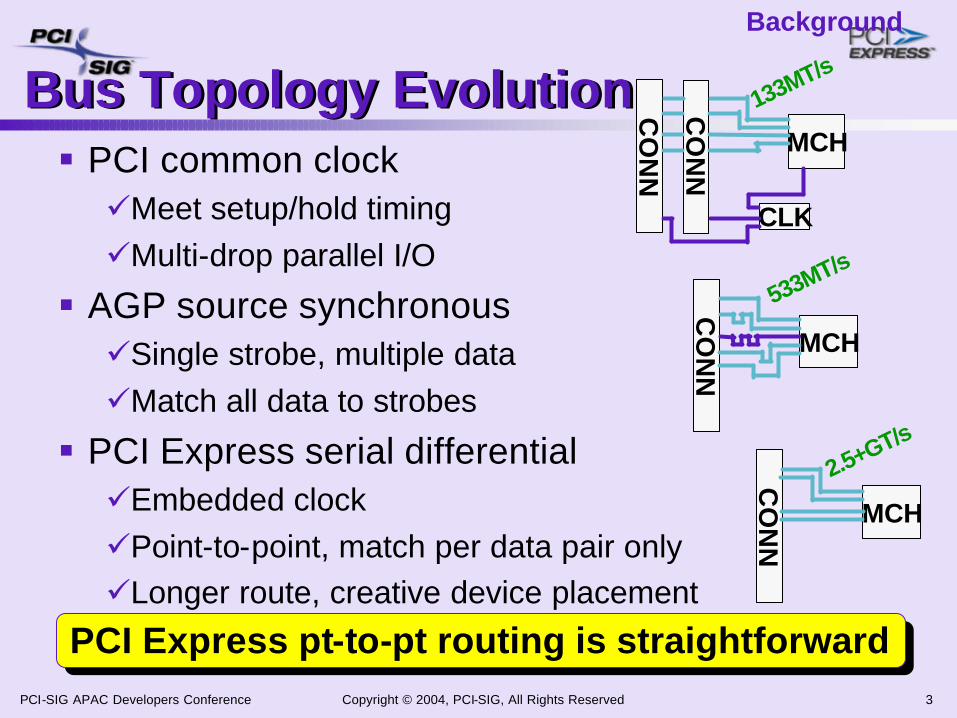
Bus Topology EvolutionBus Topology Evolution§ PCI common clock üMeet setup/hold timingüMulti-drop parallel I/O
§ AGP source synchronousüSingle strobe, multiple dataüMatch all data to strobes
§ PCI Express serial differentialüEmbedded clocküPoint-to-point, match per data pair onlyüLonger route, creative device placement
CO
NN
MCH
CO
NN
MCH
CO
NN
MCH
CLK
CO
NN
133MT/s
533MT/s
2.5+GT/s
PCI Express pt-to-pt routing is straightforwardPCI Express pt-to-pt routing is straightforward
Background
Copyright © 2004, PCI-SIG, All Rights Reserved 4PCI-SIG APAC Developers Conference
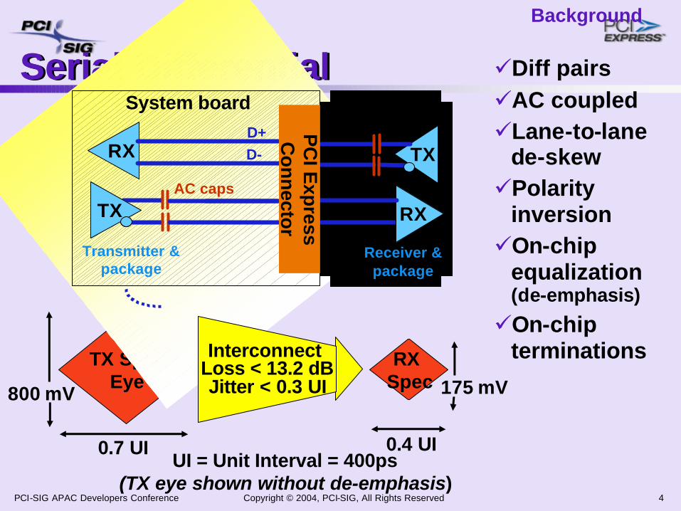
Serial DifferentialSerial Differential üDiff pairsüAC coupledüLane-to-lane
de-skew üPolarity
inversionüOn-chip
equalization (de-emphasis)
üOn-chip terminations
Background
TX SpecEye
RX Spec
UI = Unit Interval = 400ps(TX eye shown without de-emphasis)
TX
System board
RXTX RX
Add-in card
RX TX
AC caps
D+D-
Transmitter & package
Receiver & package
0.7 UI
800 mV
0.4 UI
175 mV
Interconnect Loss < 13.2 dBJitter < 0.3 UI
PC
I Exp
ressC
onnector
Copyright © 2004, PCI-SIG, All Rights Reserved 5PCI-SIG APAC Developers Conference
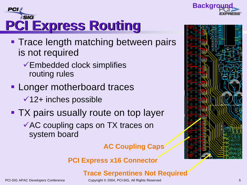
§ Trace length matching between pairs is not requiredüEmbedded clock simplifies
routing rules
§ Longer motherboard tracesü12+ inches possible
§ TX pairs usually route on top layerüAC coupling caps on TX traces on
system board
Background
PCI Express x16 Connector
Trace Serpentines Not Required
AC Coupling Caps
PCI Express RoutingPCI Express Routing
Copyright © 2004, PCI-SIG, All Rights Reserved 6PCI-SIG APAC Developers Conference
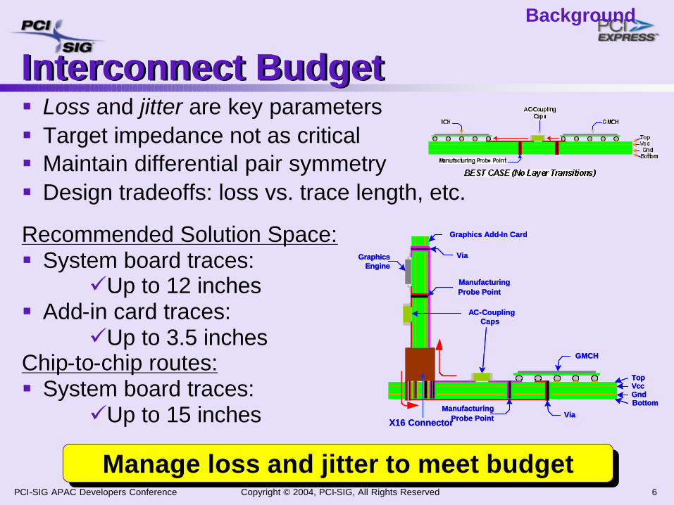
Manage loss and jitter to meet budgetManage loss and jitter to meet budget
Interconnect BudgetInterconnect Budget
Background
AC-CouplingCaps
GMCH
ViaManufacturing
Probe PointX16 Connector
VccGnd
Top
Bottom
Graphics Add-In Card
GraphicsEngine
Via
ManufacturingProbe Point
AC-CouplingCaps
GMCH
ViaManufacturing
Probe PointX16 Connector
VccGnd
Top
Bottom
Graphics Add-In Card
GraphicsEngine
Via
ManufacturingProbe Point
§ Loss and jitter are key parameters§ Target impedance not as critical§ Maintain differential pair symmetry§ Design tradeoffs: loss vs. trace length, etc.
Recommended Solution Space:§ System board traces:
üUp to 12 inches§ Add-in card traces:
üUp to 3.5 inchesChip-to-chip routes:§ System board traces:
üUp to 15 inches
Copyright © 2004, PCI-SIG, All Rights Reserved 7PCI-SIG APAC Developers Conference
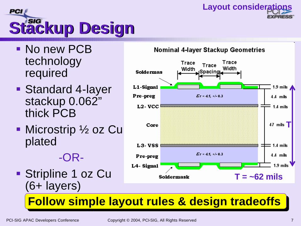
Stackup DesignStackup Design§ No new PCB
technology required§ Standard 4-layer
stackup 0.062” thick PCB§ Microstrip ½ oz Cu
plated -OR-
§ Stripline 1 oz Cu (6+ layers)
Follow simple layout rules & design tradeoffs Follow simple layout rules & design tradeoffs
Layout considerations
T = ~62 mils
T
Copyright © 2004, PCI-SIG, All Rights Reserved 8PCI-SIG APAC Developers Conference
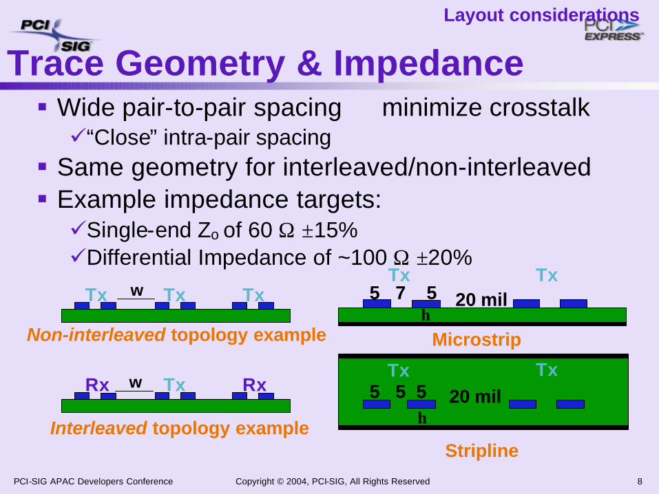
§ Wide pair-to-pair spacing ⇒ minimize crosstalkü“Close” intra-pair spacing
§ Same geometry for interleaved/non-interleaved§ Example impedance targets:üSingle-end Zo of 60 Ω ±15% üDifferential Impedance of ~100 Ω ±20%
Trace Geometry & ImpedanceLayout considerations
Non-interleaved topology example
Interleaved topology example
Rx Tx Rx
Tx Tx Txh
20 mil5 7 5
20 mil5 5 5
Microstrip
Stripline
Tx
Tx
Tx
Txw
w
h
Copyright © 2004, PCI-SIG, All Rights Reserved 9PCI-SIG APAC Developers Conference
FR4 Loss Considerations FR4 Loss Considerations § Stackup: FR4 materialüNarrow traces ⇒ loss ↑üCopper roughness ⇒ loss ↑üDielectrics with more resin material
⇒ loss ↑
§ Non-homogeneous dielectrics
üLocalized Zo variation due to material weave ⇒ loss ↑
§ Wide differential impedance variation on µstrip tracesüEtching and plating process ⇒
Resin Material
Glass Material
FR4 cross-section
Layout considerations
loss ↑
Copyright © 2004, PCI-SIG, All Rights Reserved 10PCI-SIG APAC Developers Conference
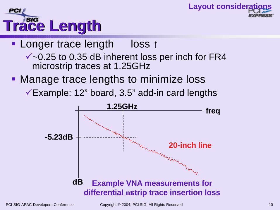
Trace LengthTrace Length§ Longer trace length ⇒ loss ↑ü~0.25 to 0.35 dB inherent loss per inch for FR4
microstrip traces at 1.25GHz§ Manage trace lengths to minimize lossüExample: 12” board, 3.5” add-in card lengths
Example VNA measurements for differential µstrip trace insertion loss
-5.23dB
1.25GHz
20-inch line
freq
dB
Layout considerations
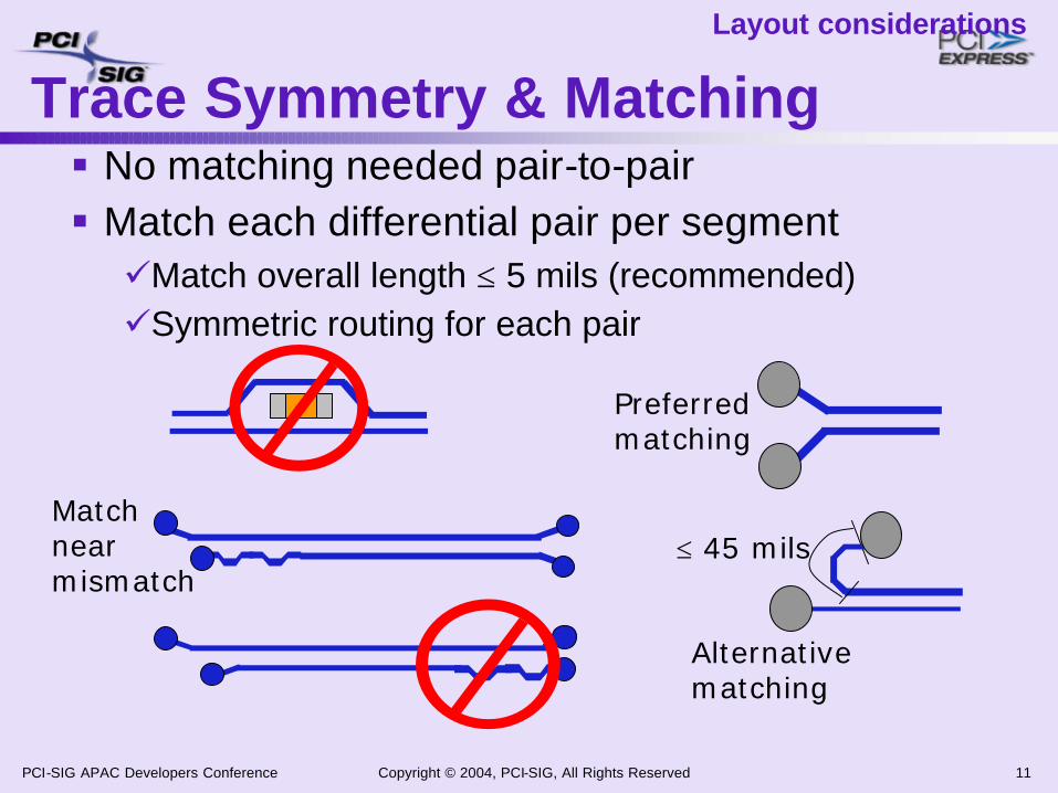
Copyright © 2004, PCI-SIG, All Rights Reserved 11PCI-SIG APAC Developers Conference
§ No matching needed pair-to-pair § Match each differential pair per segmentüMatch overall length ≤ 5 mils (recommended)üSymmetric routing for each pair
Trace Symmetry & MatchingLayout considerations
Match near mismatch
Preferred matching
Alternative matching
≤ 45 mils
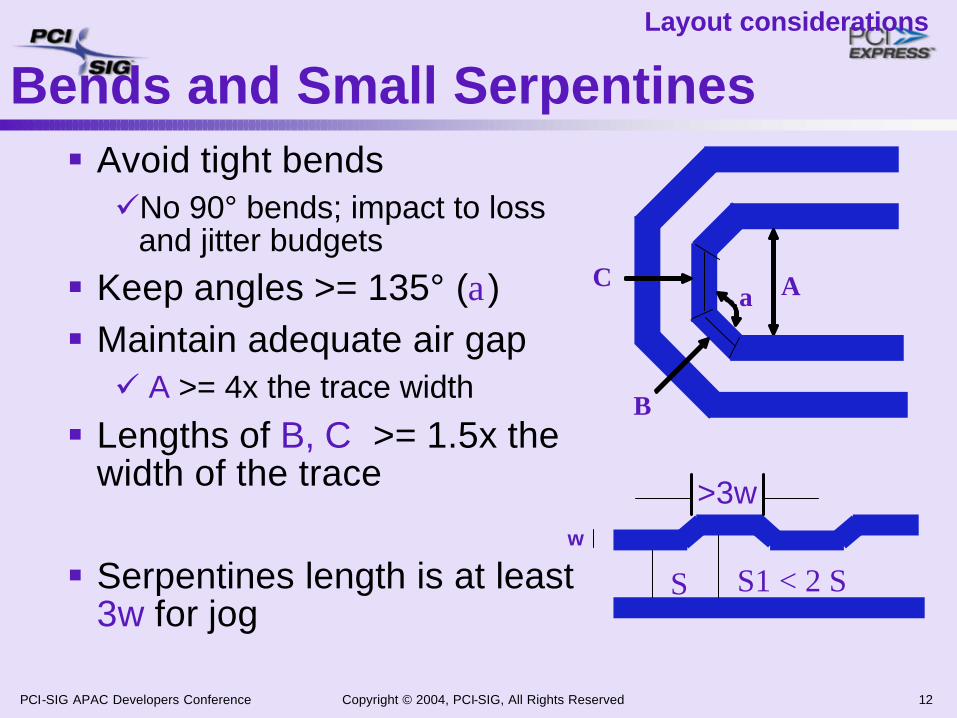
Copyright © 2004, PCI-SIG, All Rights Reserved 12PCI-SIG APAC Developers Conference
§ Avoid tight bendsüNo 90° bends; impact to loss
and jitter budgets
§ Keep angles >= 135° (a)§ Maintain adequate air gapü A >= 4x the trace width
§ Lengths of B, C >= 1.5x the width of the trace
§ Serpentines length is at least 3w for jog
Bends and Small SerpentinesLayout considerations
A
B
Cα
S S1 < 2 S
>3ww
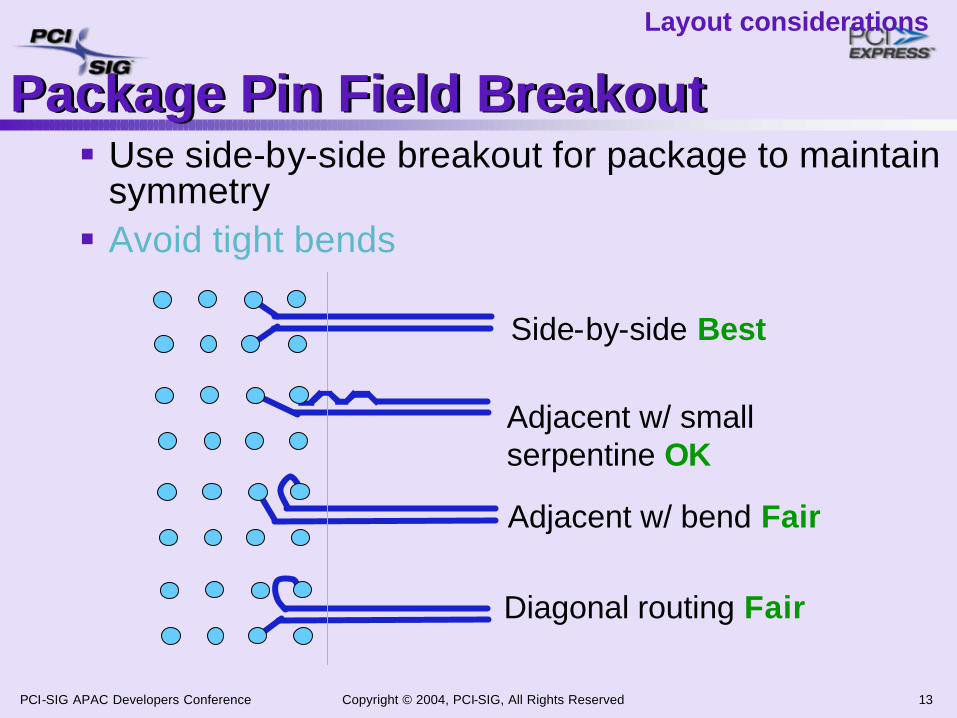
Copyright © 2004, PCI-SIG, All Rights Reserved 13PCI-SIG APAC Developers Conference
Package Pin Field BreakoutPackage Pin Field Breakout§ Use side-by-side breakout for package to maintain
symmetry§ Avoid tight bends
Layout considerations
Side-by-side Best
Adjacent w/ small serpentine OK
Adjacent w/ bend Fair
Diagonal routing Fair
Copyright © 2004, PCI-SIG, All Rights Reserved 14PCI-SIG APAC Developers Conference
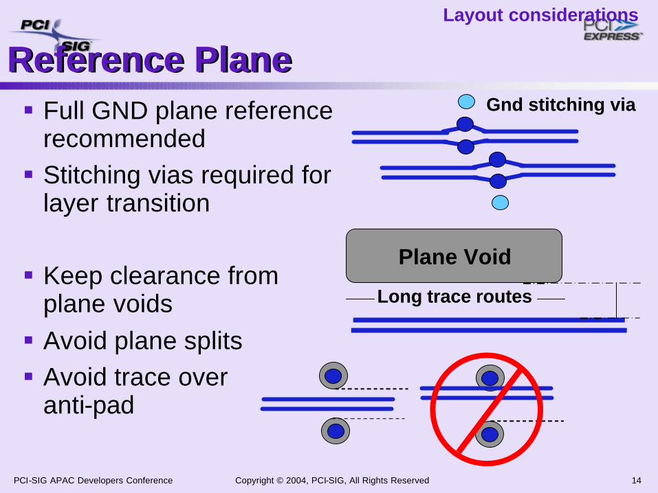
Reference PlaneReference Plane§ Full GND plane reference
recommended§ Stitching vias required for
layer transition
§ Keep clearance from plane voids§ Avoid plane splits§ Avoid trace over
anti-pad
Layout considerations
Plane Void
Gnd stitching via
Long trace routes
Copyright © 2004, PCI-SIG, All Rights Reserved 15PCI-SIG APAC Developers Conference
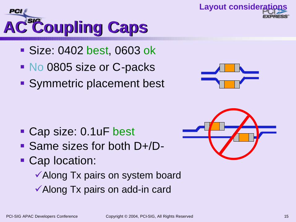
AC Coupling CapsAC Coupling Caps§ Size: 0402 best, 0603 ok§ No 0805 size or C-packs§ Symmetric placement best
§ Cap size: 0.1uF best§ Same sizes for both D+/D-§ Cap location: üAlong Tx pairs on system boardüAlong Tx pairs on add-in card
Layout considerations
Copyright © 2004, PCI-SIG, All Rights Reserved 16PCI-SIG APAC Developers Conference
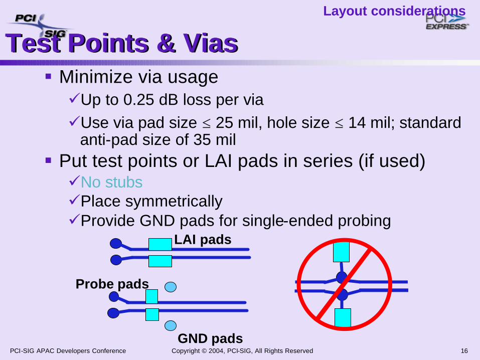
Test Points & ViasTest Points & Vias§ Minimize via usageüUp to 0.25 dB loss per viaüUse via pad size ≤ 25 mil, hole size ≤ 14 mil; standard
anti-pad size of 35 mil § Put test points or LAI pads in series (if used)üNo stubsüPlace symmetricallyüProvide GND pads for single-ended probing
LAI pads
GND pads
Probe pads
Layout considerations
Copyright © 2004, PCI-SIG, All Rights Reserved 17PCI-SIG APAC Developers Conference
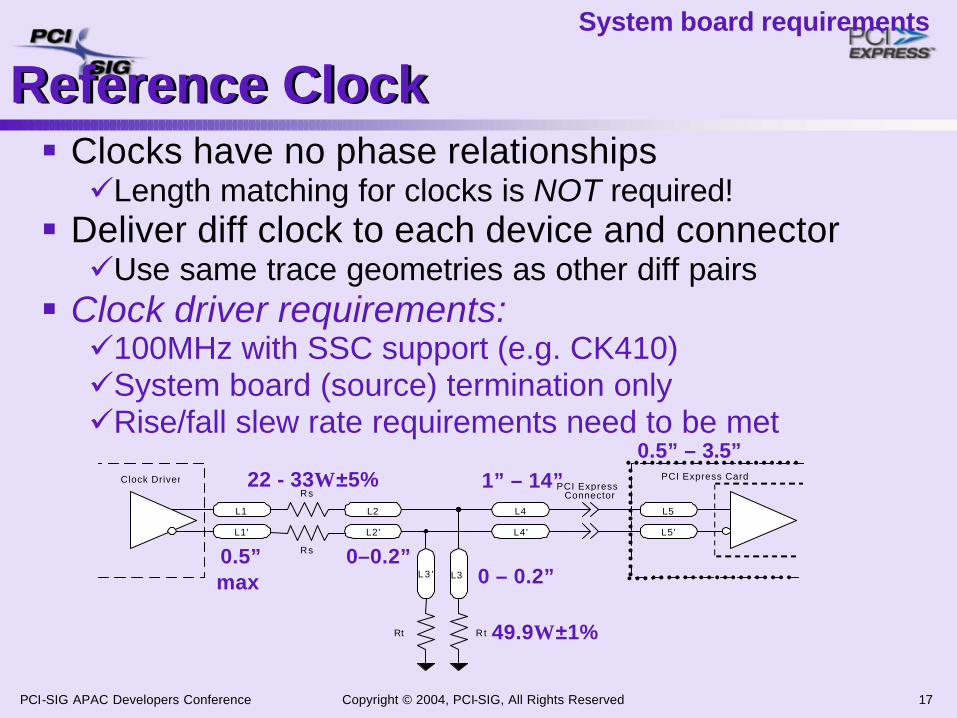
Reference ClockReference Clock§ Clocks have no phase relationshipsüLength matching for clocks is NOT required!
§ Deliver diff clock to each device and connectorüUse same trace geometries as other diff pairs
§ Clock driver requirements:ü100MHz with SSC support (e.g. CK410)üSystem board (source) termination onlyüRise/fall slew rate requirements need to be met
System board requirements
L1 L1'
L2 L2'
L3 L 3 '
L5 L5'
Rs
Rs
Rt Rt
PCI Express Connector
Clock Driver PCI Express Card
L4 L4'
0.5”max
0–0.2”0 – 0.2”
1” – 14”0.5” – 3.5”
49.9Ω ±1%
22 - 33Ω ±5%
Copyright © 2004, PCI-SIG, All Rights Reserved 18PCI-SIG APAC Developers Conference
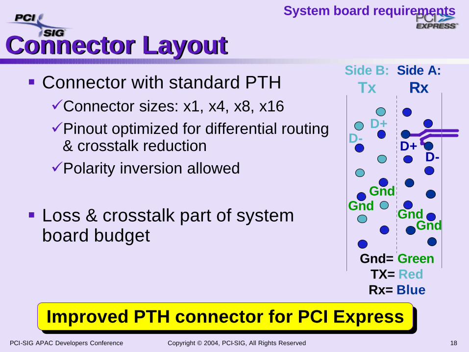
Connector LayoutConnector Layout§ Connector with standard PTHüConnector sizes: x1, x4, x8, x16 üPinout optimized for differential routing
& crosstalk reductionüPolarity inversion allowed
§ Loss & crosstalk part of system board budget
System board requirements
Improved PTH connector for PCI ExpressImproved PTH connector for PCI Express
Side B:Tx
Side A:Rx
D+D-
D+D-
GndGnd
Gnd= GreenTX= Red Rx= Blue
GndGnd
Copyright © 2004, PCI-SIG, All Rights Reserved 19PCI-SIG APAC Developers Conference
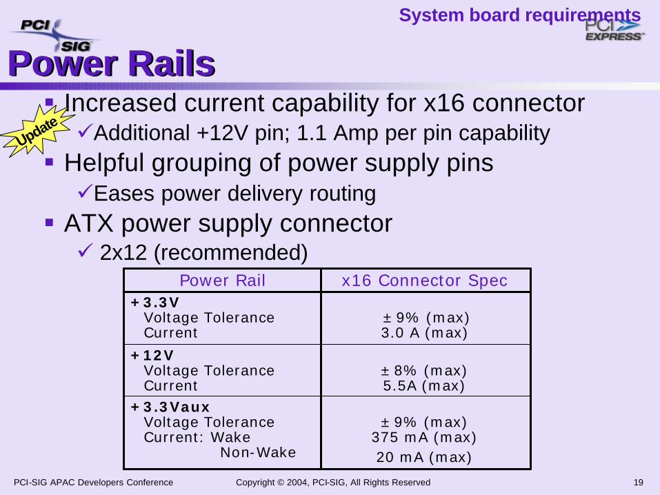
Power RailsPower Rails§ Increased current capability for x16 connectorüAdditional +12V pin; 1.1 Amp per pin capability
§ Helpful grouping of power supply pinsüEases power delivery routing
§ ATX power supply connectorü 2x12 (recommended)
± 9% (max)375 mA (max)20 mA (max)
+3.3VauxVoltage ToleranceCurrent: Wake
Non-Wake
± 8% (max)5.5A (max)
+12VVoltage ToleranceCurrent
± 9% (max)3.0 A (max)
+3.3VVoltage ToleranceCurrent
x16 Connector SpecPower Rail
System board requirements
Update
Copyright © 2004, PCI-SIG, All Rights Reserved 20PCI-SIG APAC Developers Conference
Update
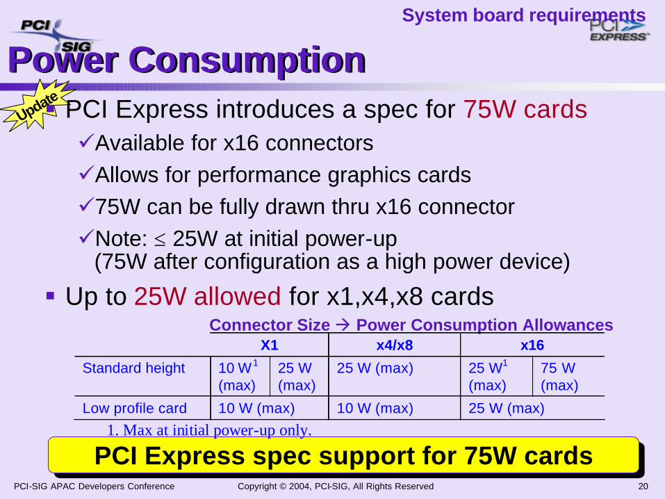
Power ConsumptionPower Consumption§ PCI Express introduces a spec for 75W cardsüAvailable for x16 connectorsüAllows for performance graphics cardsü75W can be fully drawn thru x16 connector üNote: ≤ 25W at initial power-up
(75W after configuration as a high power device)
§ Up to 25W allowed for x1,x4,x8 cards
System board requirements
Connector Size à Power Consumption Allowances
PCI Express spec support for 75W cardsPCI Express spec support for 75W cards
X1 x4/x8 x16
Standard height 10 W1 (max)
25 W (max)
25 W (max) 25 W1 (max)
75 W (max)
Low profile card 10 W (max) 10 W (max) 25 W (max)
1. Max at initial power-up only.
Copyright © 2004, PCI-SIG, All Rights Reserved 21PCI-SIG APAC Developers Conference
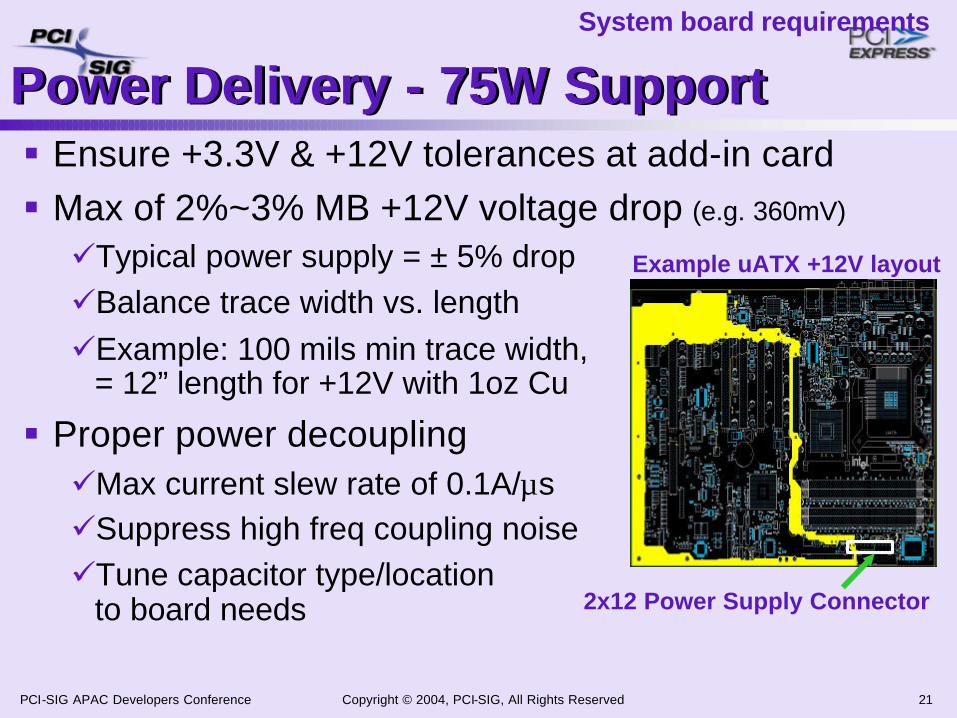
§ Ensure +3.3V & +12V tolerances at add-in card § Max of 2%~3% MB +12V voltage drop (e.g. 360mV)
üTypical power supply = ± 5% dropüBalance trace width vs. lengthüExample: 100 mils min trace width,
= 12” length for +12V with 1oz Cu
§ Proper power decoupling üMax current slew rate of 0.1A/µs üSuppress high freq coupling noiseüTune capacitor type/location
to board needs
Power Delivery - 75W SupportPower Delivery - 75W SupportSystem board requirements
Example uATX +12V layout
2x12 Power Supply Connector
Copyright © 2004, PCI-SIG, All Rights Reserved 22PCI-SIG APAC Developers Conference
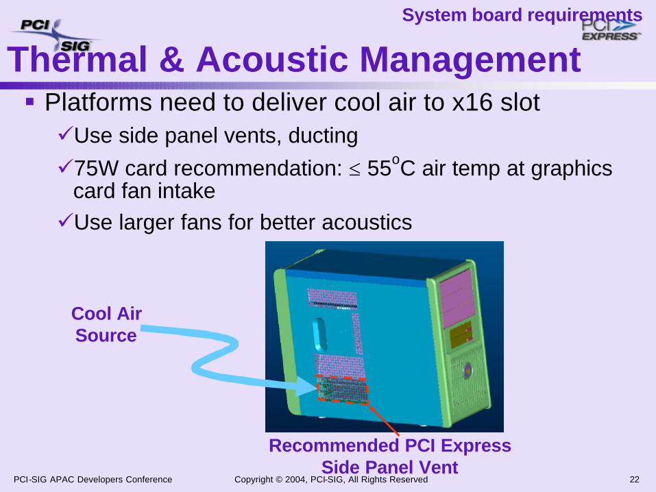
§ Platforms need to deliver cool air to x16 slotüUse side panel vents, ducting ü75W card recommendation: ≤ 55oC air temp at graphics
card fan intake üUse larger fans for better acoustics
Thermal & Acoustic ManagementSystem board requirements
Recommended PCI ExpressSide Panel Vent
Cool Air Source
Copyright © 2004, PCI-SIG, All Rights Reserved 23PCI-SIG APAC Developers Conference
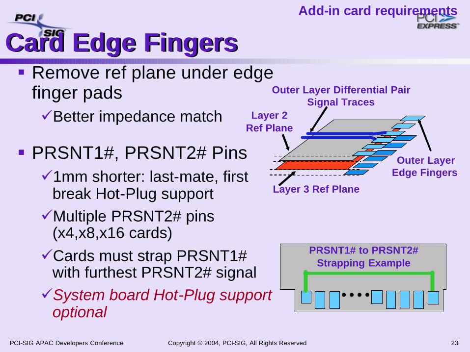
Card Edge FingersCard Edge Fingers§ Remove ref plane under edge
finger padsüBetter impedance match
§ PRSNT1#, PRSNT2# Pins ü1mm shorter: last-mate, first
break Hot-Plug supportüMultiple PRSNT2# pins
(x4,x8,x16 cards)üCards must strap PRSNT1#
with furthest PRSNT2# signal üSystem board Hot-Plug support
optional
Add-in card requirements
Layer 2 Ref Plane
Layer 3 Ref Plane
Outer Layer Differential Pair Signal Traces
Outer Layer Edge Fingers
PRSNT1# to PRSNT2# Strapping Example
Copyright © 2004, PCI-SIG, All Rights Reserved 24PCI-SIG APAC Developers Conference
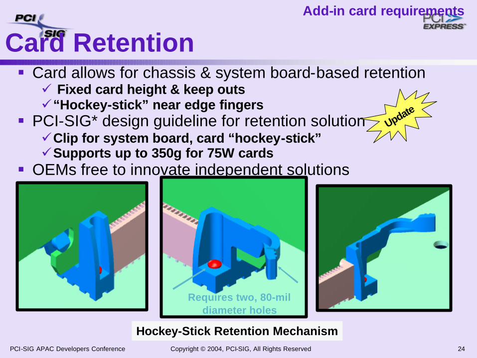
§ Card allows for chassis & system board-based retention ü Fixed card height & keep outsü“Hockey-stick” near edge fingers
§ PCI-SIG* design guideline for retention solution üClip for system board, card “hockey-stick”üSupports up to 350g for 75W cards
§ OEMs free to innovate independent solutions
Update
Card RetentionAdd-in card requirements
Hockey-Stick Retention Mechanism
Requires two, 80-mil diameter holes
Copyright © 2004, PCI-SIG, All Rights Reserved 25PCI-SIG APAC Developers Conference
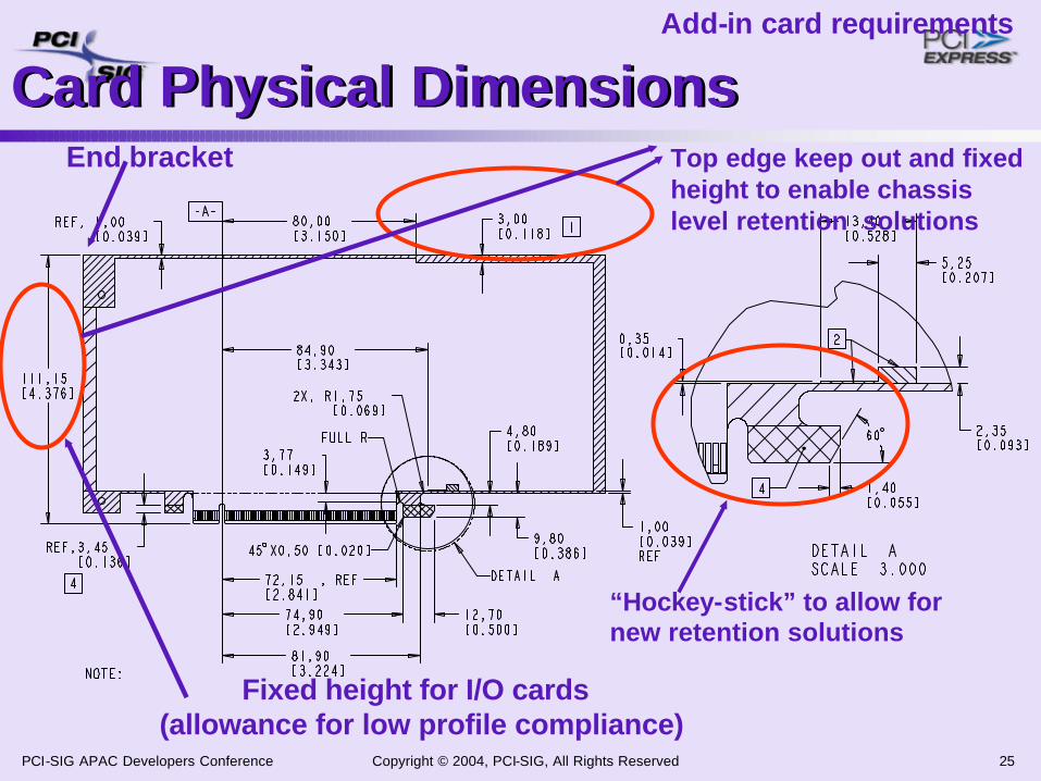
Card Physical DimensionsCard Physical DimensionsTop edge keep out and fixed height to enable chassis level retention solutions
“Hockey-stick” to allow for new retention solutions
Fixed height for I/O cards (allowance for low profile compliance)
End bracket
Add-in card requirements
Copyright © 2004, PCI-SIG, All Rights Reserved 26PCI-SIG APAC Developers Conference
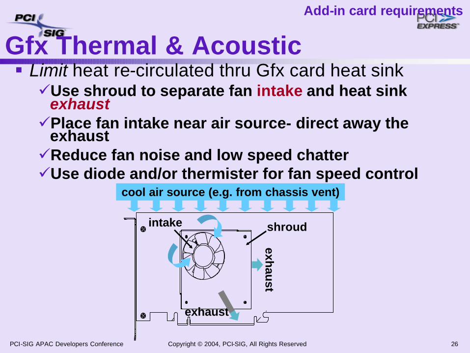
§ Limit heat re-circulated thru Gfx card heat sinküUse shroud to separate fan intake and heat sink
exhaust üPlace fan intake near air source- direct away the
exhaustüReduce fan noise and low speed chatterüUse diode and/or thermister for fan speed control
Gfx Thermal & AcousticAdd-in card requirements
exhaust
exhau
stcool air source (e.g. from chassis vent)
intake shroud
Copyright © 2004, PCI-SIG, All Rights Reserved 27PCI-SIG APAC Developers Conference
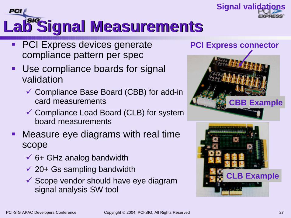
Lab Signal MeasurementsLab Signal Measurements§ PCI Express devices generate
compliance pattern per spec§ Use compliance boards for signal
validation ü Compliance Base Board (CBB) for add-in
card measurementsü Compliance Load Board (CLB) for system
board measurements
§ Measure eye diagrams with real time scopeü 6+ GHz analog bandwidthü 20+ Gs sampling bandwidthü Scope vendor should have eye diagram
signal analysis SW tool
Signal validations
CBB Example
CLB Example
PCI Express connector
Copyright © 2004, PCI-SIG, All Rights Reserved 28PCI-SIG APAC Developers Conference
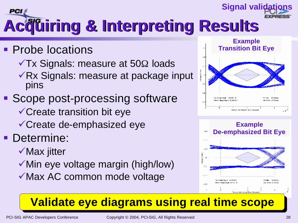
Acquiring & Interpreting ResultsAcquiring & Interpreting Results§ Probe locationsüTx Signals: measure at 50Ω loadsüRx Signals: measure at package input
pins§ Scope post-processing softwareüCreate transition bit eyeüCreate de-emphasized eye
§ Determine:üMax jitterüMin eye voltage margin (high/low)üMax AC common mode voltage
Example Example Transition Bit EyeTransition Bit Eye
Example Example DeDe--emphasized Bit Eyeemphasized Bit Eye
Signal validations
Validate eye diagrams using real time scopeValidate eye diagrams using real time scope
Copyright © 2004, PCI-SIG, All Rights Reserved 29PCI-SIG APAC Developers Conference
SummarySummary§ PCI Express point-to-point layout is
straightforward§ Manage loss and jitter from PCB to meet
interconnect budget§ Follow basic layout rules and design tradeoffs to
implement typical topologies§ Improved connector & add-in card features -
support for 75 Watt cards § Validate compliance eye diagrams using
compliance boards and real time scope
Summary
Copyright © 2004, PCI-SIG, All Rights Reserved 30PCI-SIG APAC Developers Conference
CollateralCollateral
§ For additional and updated information on PCI Express Architecture, visit
http://www.pcisig.com
Copyright © 2004, PCI-SIG, All Rights Reserved 31PCI-SIG APAC Developers Conference
Thank you for attending the 2004 PCI-SIG Asia-Pacific Developers Conference.
For more information please go to www.pcisig.com
Copyright © 2004, PCI-SIG, All Rights Reserved 32PCI-SIG APAC Developers Conference


![f a reassembled PDU] - Texas Instrumentse2e.ti.com/cfs-file/__key/communityserver-discussions-components... · 2050 86.673954000 192.168.1.103 192.168.1.100 ... [TCP segment o f a](https://img.pdfslide.net/doc/110x75/5b05c4e67f8b9a93418bcf7a/f-a-reassembled-pdu-texas-86673954000-1921681103-1921681100-tcp-segment.jpg)