Embed Size (px)
DESCRIPTION
Boost Conveter Battery and Solar Cell Operation Sensor Network
Citation preview
IEEE JOURNAL OF SOLID-STATE CIRCUITS, VOL. 48, NO. 8, AUGUST 2013 1933
0.5 V Start-Up 87% Efficiency 0.75 mm² On-ChipFeed-Forward Single-Inductor Dual-Output(SIDO) Boost DC-DC Converter for Batteryand Solar Cell Operation Sensor Network
Micro-Computer IntegrationYasunobu Nakase, Shinichi Hirose, Hiroshi Onoda, Yasuhiro Ido, Yoshiaki Shimizu, Tsukasa Oishi,
Toshio Kumamoto, and Toru Shimizu, Senior Member, IEEE
Abstract—An on-chip low power single-inductor dual-output(SIDO) DC-DC boost converter is proposed for battery and solarcell operating sensor network applications. A proposed feedforward control determines the Ton/Toff ratio precisely for eachoutput without any compensation or linear capacitor. This featurehelps reduce the costs of the external components and utilizean inexpensive process technology. A test chip was fabricated by190-nm flash-memory embedded micro-computers CMOS processtechnology and can achieve an efficiency of 87% with a small areasize of just 0.75 mm². For solar cell operation, a 0.5 V start-upwas achieved even with a high threshold voltage of 0.7 V with aproposed forward back biased charge pump. A constant voltagealgorithm was implemented as a maximum power point tracking(MPPT) control. With this MPPT control, a solar cell with an openvoltage of 1.03 V and a short current of 83 mA was able to chargea super capacitor of 0.4 F up to 5 V within 80 s.
Index Terms—Boost, DC-DC converter, energy harvesting, feedforward control.
I. INTRODUCTION
R ECENTLY, wireless sensor networks have been widelyused to improve energy efficiency by controlling
building, office, and home environments [1]–[3]. A largenumber of sensor nodes are distributed to monitor environ-mental parameters such as temperature, humidity, illuminationintensity, and so on. Each node consists of a micro-computer forcontrolling the node operation, sensors, and sensor interfaces
Manuscript received November 29, 2012; revised March 28, 2013; acceptedMarch 28, 2013. Date of publication May 13, 2013; date of current version July19, 2013. This paper was approved by Guest Editor Ken Suyama.Y. Nakase, Y. Ido, and T. Kumamoto are with the Core Technology Business
Division, Renesas Electronics Corporation, Hyogo 664-0005, Japan (e-mail:[email protected]).T. Oishi and Y. Shimizu are with Fundamental Technology Unit, Renesas
Design Corporation, Hyogo 664-0005, Japan.S. Hirose and H. Onoda are with Renesas Design Corporation, Hyogo 664-
0005, Japan.T. Shimizu is with Global Business Innovation and Strategy Marketing Divi-
sion, 1st Solution Business Unit, Renesas Electronics Corporation, Tokyo 100-0004, Japan.Color versions of one or more of the figures in this paper are available online
at http://ieeexplore.ieee.org.Digital Object Identifier 10.1109/JSSC.2013.2258826
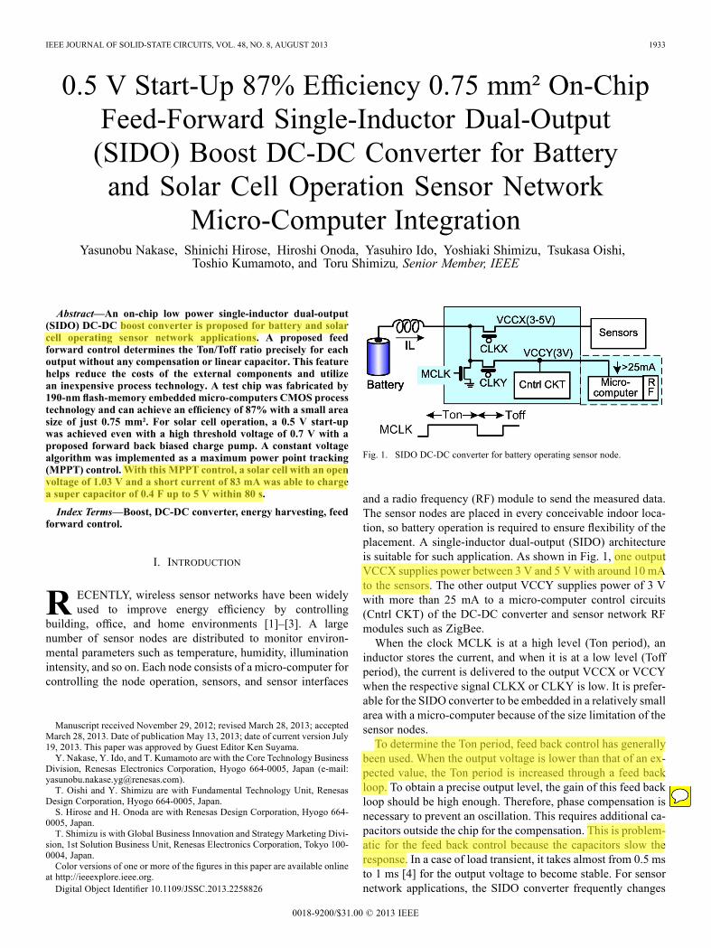
Fig. 1. SIDO DC-DC converter for battery operating sensor node.
and a radio frequency (RF) module to send the measured data.The sensor nodes are placed in every conceivable indoor loca-tion, so battery operation is required to ensure flexibility of theplacement. A single-inductor dual-output (SIDO) architectureis suitable for such application. As shown in Fig. 1, one outputVCCX supplies power between 3 V and 5 V with around 10 mAto the sensors. The other output VCCY supplies power of 3 Vwith more than 25 mA to a micro-computer control circuits(Cntrl CKT) of the DC-DC converter and sensor network RFmodules such as ZigBee.When the clock MCLK is at a high level (Ton period), an
inductor stores the current, and when it is at a low level (Toffperiod), the current is delivered to the output VCCX or VCCYwhen the respective signal CLKX or CLKY is low. It is prefer-able for the SIDO converter to be embedded in a relatively smallarea with a micro-computer because of the size limitation of thesensor nodes.To determine the Ton period, feed back control has generally
been used. When the output voltage is lower than that of an ex-pected value, the Ton period is increased through a feed backloop. To obtain a precise output level, the gain of this feed backloop should be high enough. Therefore, phase compensation isnecessary to prevent an oscillation. This requires additional ca-pacitors outside the chip for the compensation. This is problem-atic for the feed back control because the capacitors slow theresponse. In a case of load transient, it takes almost from 0.5 msto 1 ms [4] for the output voltage to become stable. For sensornetwork applications, the SIDO converter frequently changes
0018-9200/$31.00 © 2013 IEEE
1934 IEEE JOURNAL OF SOLID-STATE CIRCUITS, VOL. 48, NO. 8, AUGUST 2013
Fig. 2. Single output DC-DC converter.
Fig. 3. Conventional discontinuous conduction mode (DCM) controls for dualoutputs.
the outputs for charging up. The Ton/Toff ratio needs to be de-termined immediately when the output changes, so feed backcontrol is not suitable for SIDO architecture. The other problemof feed back control can be explained simply by using a singleoutput boost converter as shown in Fig. 2. The transfer functionis given by [5]
(1)
(2)
The transfer function depends on all of the parameters. Foreach different value of L, C, R, Vin, and Vout, compensationcircuits should be optimized. Therefore, it is difficult to supporta wide range of input and output voltages and the values of L,C, and R.Many types of discontinuous conduction mode (DCM) oper-
ation have been proposed as methods that do not require com-pensation. Fig. 3 (i) shows a case in which each output is alter-nately charged in every cycle [6], [7]. In Fig. 3 (ii), both outputsare charged in every cycle [8]. Large transistors are necessaryin DCM to obtain a high efficiency because the peak inductorcurrent is large. Fig. 3 (iii) shows the pseudo continuous conduc-tion mode (CCM). The peak inductor current IL can be reducedby flowing a constant current [9]. This mode has achieved ef-ficiencies of 88.4% and 89.4% with chip sizes of 2.4 mm [6]and 4.25 mm [9], respectively. These sizes, however, are toolarge for micro-computer integration. Furthermore, each outputis required to supply almost the same amount of load current in[9] to keep the offset current at a constant level.Feed forward control [10] is another method that does not
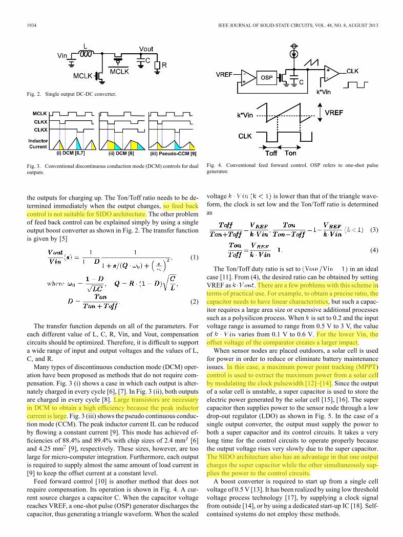
require compensation. Its operation is shown in Fig. 4. A cur-rent source charges a capacitor C. When the capacitor voltagereaches VREF, a one-shot pulse (OSP) generator discharges thecapacitor, thus generating a triangle waveform.When the scaled
Fig. 4. Conventional feed forward control. OSP refers to one-shot pulsegenerator.
voltage is lower than that of the triangle wave-form, the clock is set low and the Ton/Toff ratio is determinedas
(3)
(4)
The Ton/Toff duty ratio is set to in an idealcase [11]. From (4), the desired ratio can be obtained by settingVREF as . There are a few problems with this scheme interms of practical use. For example, to obtain a precise ratio, thecapacitor needs to have linear characteristics, but such a capac-itor requires a large area size or expensive additional processessuch as a polysilicon process. When is set to 0.2 and the inputvoltage range is assumed to range from 0.5 V to 3 V, the valueof varies from 0.1 V to 0.6 V. For the lower Vin, theoffset voltage of the comparator creates a larger impact.When sensor nodes are placed outdoors, a solar cell is used
for power in order to reduce or eliminate battery maintenanceissues. In this case, a maximum power point tracking (MPPT)control is used to extract the maximum power from a solar cellby modulating the clock pulsewidth [12]–[14]. Since the outputof a solar cell is unstable, a super capacitor is used to store theelectric power generated by the solar cell [15], [16]. The supercapacitor then supplies power to the sensor node through a lowdrop-out regulator (LDO) as shown in Fig. 5. In the case of asingle output converter, the output must supply the power toboth a super capacitor and its control circuits. It takes a verylong time for the control circuits to operate properly becausethe output voltage rises very slowly due to the super capacitor.The SIDO architecture also has an advantage in that one outputcharges the super capacitor while the other simultaneously sup-plies the power to the control circuits.A boost converter is required to start up from a single cell
voltage of 0.5 V [13]. It has been realized by using low thresholdvoltage process technology [17], by supplying a clock signalfrom outside [14], or by using a dedicated start-up IC [18]. Self-contained systems do not employ these methods.
NAKASE et al.: ON-CHIP FEED-FORWARD SIDO BOOST DC-DC CONVERTER 1935
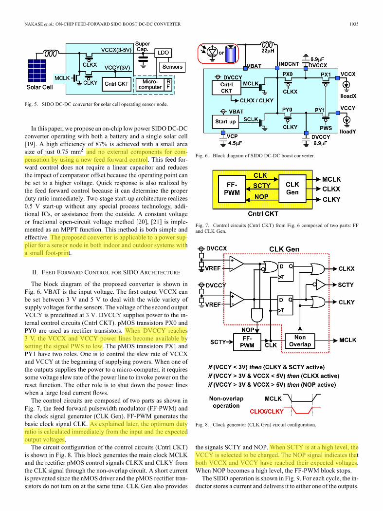
Fig. 5. SIDO DC-DC converter for solar cell operating sensor node.
In this paper, we propose an on-chip low power SIDODC-DCconverter operating with both a battery and a single solar cell[19]. A high efficiency of 87% is achieved with a small areasize of just 0.75 mm and no external components for com-pensation by using a new feed forward control. This feed for-ward control does not require a linear capacitor and reducesthe impact of comparator offset because the operating point canbe set to a higher voltage. Quick response is also realized bythe feed forward control because it can determine the properduty ratio immediately. Two-stage start-up architecture realizes0.5 V start-up without any special process technology, addi-tional ICs, or assistance from the outside. A constant voltageor fractional open-circuit voltage method [20], [21] is imple-mented as an MPPT function. This method is both simple andeffective. The proposed converter is applicable to a power sup-plier for a sensor node in both indoor and outdoor systems witha small foot-print.
II. FEED FORWARD CONTROL FOR SIDO ARCHITECTURE
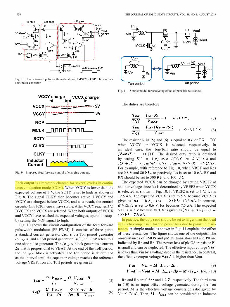
The block diagram of the proposed converter is shown inFig. 6. VBAT is the input voltage. The first output VCCX canbe set between 3 V and 5 V to deal with the wide variety ofsupply voltages for the sensors. The voltage of the second outputVCCY is predefined at 3 V. DVCCY supplies power to the in-ternal control circuits (Cntrl CKT). pMOS transistors PX0 andPY0 are used as rectifier transistors. When DVCCY reaches3 V, the VCCX and VCCY power lines become available bysetting the signal PWS to low. The pMOS transistors PX1 andPY1 have two roles. One is to control the slew rate of VCCXand VCCY at the beginning of supplying powers. When one ofthe outputs supplies the power to a micro-computer, it requiressome voltage slew rate of the power line to invoke power on thereset function. The other role is to shut down the power lineswhen a large load current flows.The control circuits are composed of two parts as shown in
Fig. 7, the feed forward pulsewidth modulator (FF-PWM) andthe clock signal generator (CLK Gen). FF-PWM generates thebasic clock signal CLK. As explained later, the optimum dutyratio is calculated immediately from the input and the expectedoutput voltages.The circuit configuration of the control circuits (Cntrl CKT)
is shown in Fig. 8. This block generates the main clock MCLKand the rectifier pMOS control signals CLKX and CLKY fromthe CLK signal through the non-overlap circuit. A short currentis prevented since the nMOS driver and the pMOS rectifier tran-sistors do not turn on at the same time. CLK Gen also provides
Fig. 6. Block diagram of SIDO DC-DC boost converter.
Fig. 7. Control circuits (Cntrl CKT) from Fig. 6 composed of two parts: FFand CLK Gen.
Fig. 8. Clock generator (CLK Gen) circuit configuration.
the signals SCTY and NOP. When SCTY is at a high level, theVCCY is selected to be charged. The NOP signal indicates thatboth VCCX and VCCY have reached their expected voltages.When NOP becomes a high level, the FF-PWM block stops.The SIDO operation is shown in Fig. 9. For each cycle, the in-
ductor stores a current and delivers it to either one of the outputs.
1936 IEEE JOURNAL OF SOLID-STATE CIRCUITS, VOL. 48, NO. 8, AUGUST 2013
Fig. 10. Feed-forward pulsewidth modulation (FF-PWM). OSP refers to one-shot pulse generator.
Fig. 9. Proposed feed-forward control of charging outputs.
Each output is alternately charged for several cycles in contin-uous conduction mode (CCM). When VCCY is lower than theexpected voltage of 3 V, the SCTY is set to high as shown inFig. 8. The signal CLKY then becomes active. DVCCY andVCCY are charged before VCCX, and as a result, the controlcircuits (Cntrl CKT) are always stable. After VCCY reaches 3 V,DVCCX and VCCX are selected. When both outputs of VCCXand VCCY have reached the expected voltages, operation stopsby setting the NOP signal to high.Fig. 10 shows the circuit configuration of the feed forward
pulsewidth modulator (FF-PWM). It consists of three parts:a standard current generator , a Ton period generator
, and a Toff period generator . OSP refers to aone-shot pulse generator. The block generates a currentthat is proportional to VBAT. At the end of the Toff period,
the block is activated. The Ton period is determinedas the interval until the capacitor voltage reaches the referencevoltage VREF. Ton and Toff periods are given as
(5)
(6)
Fig. 11. Simple model for analyzing effect of parasitic resistances.
The duties are therefore
(7)
(8)
The resistor R in (5) and (6) is equal to RY orwhen VCCY or VCCX is selected, respectively. Inan ideal case, the Ton/Toff ratio should be equal to
[11]. The desired duty ratio is obtainedby setting and
.For example, with reference to Fig. 10, when VREF and Rcsare 0.8 V and 80 , respectively, Ics is set to 10 A. RY andRX should be set to 300 and 100 .The expected VCCX can be changed by setting VREF2 at
another voltage since Ics is determined by VREF2 when VCCXis selected as shown in Fig. 10. If VREF2 is set to 1 V, Ics is12.5 A. The expected VCCX is set to 5 V because VCCX isgiven as A. In contrast,if VREF2 is set to 0.6 V, Ics becomes 7.5 A. The expectedVCCX is 3 V because VCCX is given as
A.In practice, the duty ratio should be set to larger than the ideal
values to compensate for the power loss due to parasitic resis-tances. A simple model as shown in Fig. 11 explains the effectof these resistances. The figure shows one of the outputs. Theon-resistances of nMOS and pMOS transistors N0 and P0 areindicated by Rn and Rp. The power loss of pMOS transistor P1is small and can be neglected. The effective input voltageis lower than Vin by a voltage drop in the resistance. In contrast,the effective output voltage is higher than Vout.
(9)
(10)
Rn and Rp are 0.5 and 1.2 , respectively. The third termin (10) is an input offset voltage generated during the Tonperiod. M is the effective voltage conversion ratio given by
. Then, can be considered an inductor
NAKASE et al.: ON-CHIP FEED-FORWARD SIDO BOOST DC-DC CONVERTER 1937
Fig. 12. Electrical characteristics of solar cell.
current. From (9) and (10), the sustainable load current can becalculated for a given M value.
(11)
As the M value is set larger than its ideal value of Vout/Vin,the sustainable load current increases. However, the power lossincreases because the inductor current increases. We thereforeset the M value to 7% larger than its ideal value. The sustainableload current of VCCX is given as follows. When the VBAT is0.5 V, the M value is . VCCXcan supply a load current of 3.7 mA. When VBAT is 1.5 V, thesustainable load current increases up to 30 mA.As shown in (11), the sustainable load current is not deter-
mined from the Ton and Toff periods themselves but rather theirratio. Equations (7) and (8) mean that the ratio is independent ofthe value of the capacitors. Therefore, capacitor linearity is notrequired in this proposed control. In practice, varactors are usedas non-linear capacitors. Furthermore, a precise ratio is obtainedeven at low VBAT. Since the comparator operates at the inputrange around VREF (0.8 V in this case), the offset voltage hasonly minimal impact compared with the conventional control.
III. OPERATION WITH SOLAR CELL
In the case of solar cell operation, anMPPT control is used in-stead of the feed forward control. Fig. 12 shows electrical char-acteristics of a solar cell. Open voltage is defined as the voltagewhen no current flows and short current is defined as the currentwhen the voltage is zero. For each point, the power is zero. Asthe Ton period increases, the solar cell current increases and itsvoltage decreases. Various methods have been proposed to op-erate a converter at the maximum power point, most of them re-quiring complicated calculation algorithms. An exception is theconstant voltage or fractional open-circuit voltage method. Thismethod takes advantage of the fact that the maximum poweris obtained at some fixed fraction (around 80%) of the openvoltage as shown in Fig. 12. The proposed converter employsthis simple method.Fig. 13 shows the main part of the control circuits for the
MPPT function. The VMON signal is asserted every 20ms froman external controller. When VMON is high, the main clockMCLK stops and the solar cell voltage is sampled. This is anopen voltage because the converter does not drive a load. A
Fig. 13. Control circuits for constant voltage maximum power point tracking(MPPT).
Fig. 14. Circuit configuration during start-up operation.
comparator CMP compares the solar cell voltage (VBAT) with80% of its open voltage. When VBAT becomes lower than 80%of its open voltage, the CLK_EN signal becomes low and theclock signal MCLK halts at a low level. In this situation, morecurrent is pulled from a solar cell than it can supply. After theinput voltage has recovered, the converter resumes operation.As a result, the duty ratio is automatically determined to operateat the maximum solar power.
IV. 0.5-V START-UP CIRCUITS OPERATION AND ANALYSIS
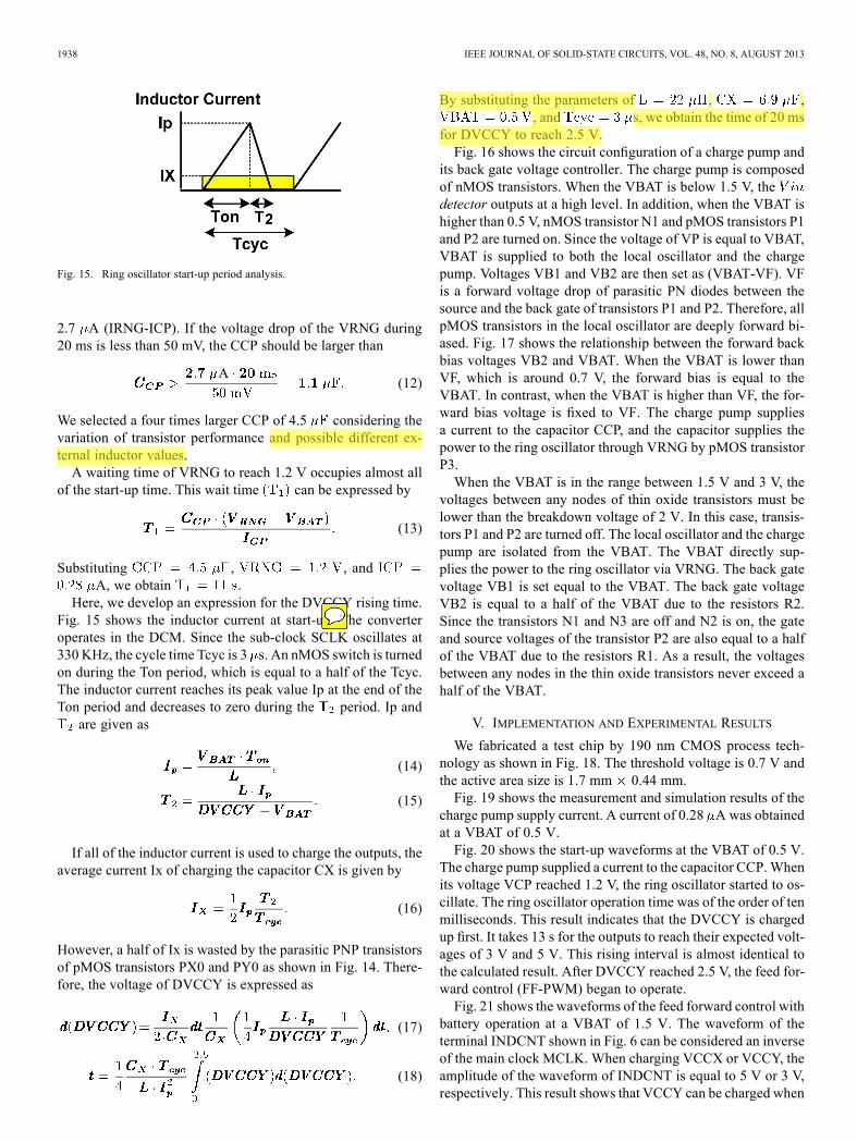
Fig. 14 shows the circuit configuration during start-up. Sincethe control circuits are inactive, the main clock MCLK is ata low level and the rectifier signals CLKX and CLKY are ata high level. The signal PWS is also at a high level. A ringoscillator (Ring Osc) supplies a substitute clock signal SCLKwith a 50% duty ratio. Since pMOS transistors PX0 and PY0are off, an inductor current charges the capacitor CX through theparasitic PN diodes of PX0 and PY0. In this period, both backgates of these pMOS transistors PX0 and PY0 are connected tothe DVCCY node.When the VBAT is higher than 1.5 V, it directly supplies
power to the ring oscillator. In contrast, when it is lower than1.5 V, a charge pump supplies the power through the VRNGnode. In this case, a charge pump supplies a current ICP to thecapacitor CCP. After the VRNG voltage reaches 1.2 V, the ringoscillator begins to operate. The ring oscillator raises the voltageof DVCCY and when it reaches 2.5 V, the feed forward con-trol is activated. As shown later, it takes 20 ms for DVCCYto rise to 2.5 V when VBAT is 0.5 V. During this period, thecharge pump supplies a current ICP of 0.28 A and the ringoscillator consumes a current IRNG of 3 A. Therefore, the ca-pacitor CCP must supply the difference of these currents, i.e.,
1938 IEEE JOURNAL OF SOLID-STATE CIRCUITS, VOL. 48, NO. 8, AUGUST 2013
Fig. 15. Ring oscillator start-up period analysis.
2.7 A (IRNG-ICP). If the voltage drop of the VRNG during20 ms is less than 50 mV, the CCP should be larger than
A(12)
We selected a four times larger CCP of 4.5 considering thevariation of transistor performance and possible different ex-ternal inductor values.A waiting time of VRNG to reach 1.2 V occupies almost all
of the start-up time. This wait time can be expressed by
(13)
Substituting , , andA, we obtain .
Here, we develop an expression for the DVCCY rising time.Fig. 15 shows the inductor current at start-up. The converteroperates in the DCM. Since the sub-clock SCLK oscillates at330 KHz, the cycle time Tcyc is 3 s. An nMOS switch is turnedon during the Ton period, which is equal to a half of the Tcyc.The inductor current reaches its peak value Ip at the end of theTon period and decreases to zero during the period. Ip andare given as
(14)
(15)
If all of the inductor current is used to charge the outputs, theaverage current Ix of charging the capacitor CX is given by
(16)
However, a half of Ix is wasted by the parasitic PNP transistorsof pMOS transistors PX0 and PY0 as shown in Fig. 14. There-fore, the voltage of DVCCY is expressed as
(17)
(18)
By substituting the parameters of , ,, and s, we obtain the time of 20 ms
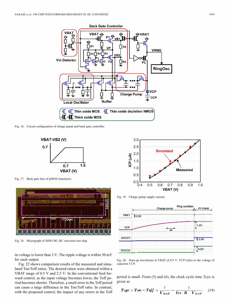
for DVCCY to reach 2.5 V.Fig. 16 shows the circuit configuration of a charge pump and
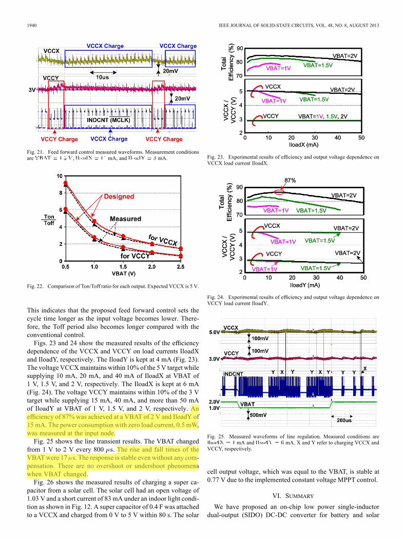
its back gate voltage controller. The charge pump is composedof nMOS transistors. When the VBAT is below 1.5 V, thedetector outputs at a high level. In addition, when the VBAT ishigher than 0.5 V, nMOS transistor N1 and pMOS transistors P1and P2 are turned on. Since the voltage of VP is equal to VBAT,VBAT is supplied to both the local oscillator and the chargepump. Voltages VB1 and VB2 are then set as (VBAT-VF). VFis a forward voltage drop of parasitic PN diodes between thesource and the back gate of transistors P1 and P2. Therefore, allpMOS transistors in the local oscillator are deeply forward bi-ased. Fig. 17 shows the relationship between the forward backbias voltages VB2 and VBAT. When the VBAT is lower thanVF, which is around 0.7 V, the forward bias is equal to theVBAT. In contrast, when the VBAT is higher than VF, the for-ward bias voltage is fixed to VF. The charge pump suppliesa current to the capacitor CCP, and the capacitor supplies thepower to the ring oscillator through VRNG by pMOS transistorP3.When the VBAT is in the range between 1.5 V and 3 V, the
voltages between any nodes of thin oxide transistors must belower than the breakdown voltage of 2 V. In this case, transis-tors P1 and P2 are turned off. The local oscillator and the chargepump are isolated from the VBAT. The VBAT directly sup-plies the power to the ring oscillator via VRNG. The back gatevoltage VB1 is set equal to the VBAT. The back gate voltageVB2 is equal to a half of the VBAT due to the resistors R2.Since the transistors N1 and N3 are off and N2 is on, the gateand source voltages of the transistor P2 are also equal to a halfof the VBAT due to the resistors R1. As a result, the voltagesbetween any nodes in the thin oxide transistors never exceed ahalf of the VBAT.
V. IMPLEMENTATION AND EXPERIMENTAL RESULTS
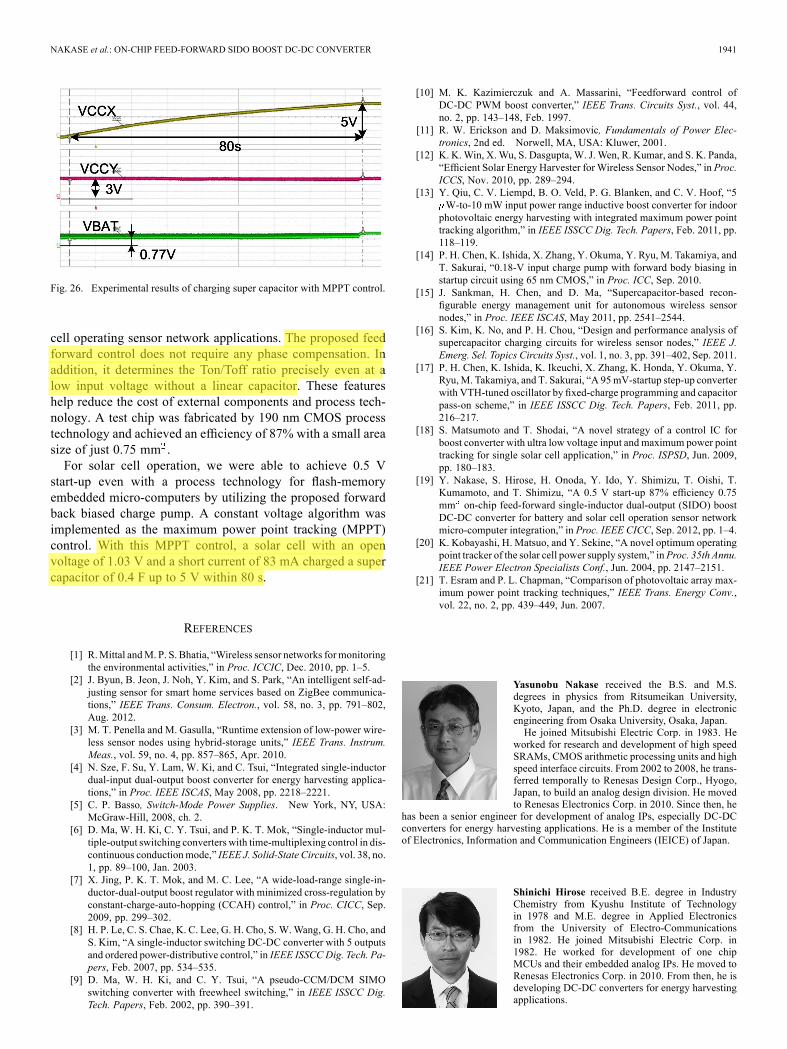
We fabricated a test chip by 190 nm CMOS process tech-nology as shown in Fig. 18. The threshold voltage is 0.7 V andthe active area size is 1.7 mm 0.44 mm.Fig. 19 shows the measurement and simulation results of the
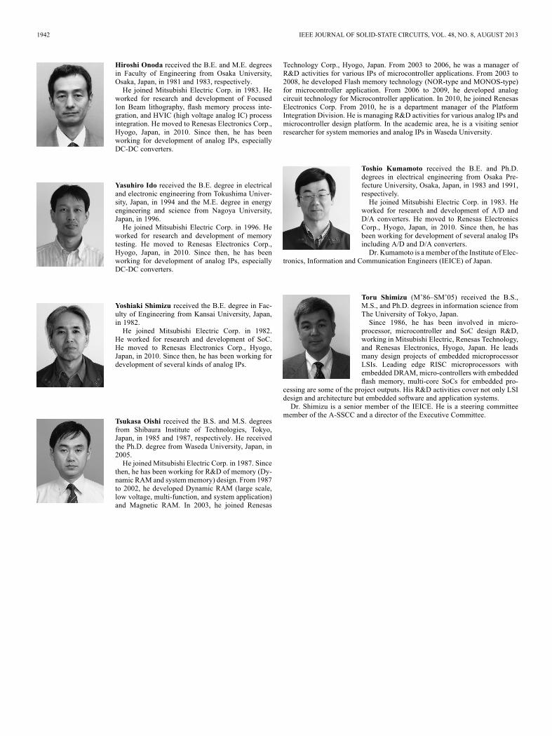
charge pump supply current. A current of 0.28 A was obtainedat a VBAT of 0.5 V.Fig. 20 shows the start-up waveforms at the VBAT of 0.5 V.
The charge pump supplied a current to the capacitor CCP.Whenits voltage VCP reached 1.2 V, the ring oscillator started to os-cillate. The ring oscillator operation time was of the order of tenmilliseconds. This result indicates that the DVCCY is chargedup first. It takes 13 s for the outputs to reach their expected volt-ages of 3 V and 5 V. This rising interval is almost identical tothe calculated result. After DVCCY reached 2.5 V, the feed for-ward control (FF-PWM) began to operate.Fig. 21 shows the waveforms of the feed forward control with
battery operation at a VBAT of 1.5 V. The waveform of theterminal INDCNT shown in Fig. 6 can be considered an inverseof the main clock MCLK. When charging VCCX or VCCY, theamplitude of the waveform of INDCNT is equal to 5 V or 3 V,respectively. This result shows that VCCY can be charged when
NAKASE et al.: ON-CHIP FEED-FORWARD SIDO BOOST DC-DC CONVERTER 1939
Fig. 16. Circuit configuration of charge pump and back gate controller.
Fig. 17. Back gate bias of pMOS transistors.
Fig. 18. Micrograph of SIDO DC-DC converter test chip.
its voltage is lower than 3 V. The ripple voltage is within 50 mVfor each output.Fig. 22 shows comparison results of the measured and simu-
lated Ton/Toff ratios. The desired ratios were obtained within aVBAT range of 0.5 V and 2.5 V. In the conventional feed for-ward control, as the input voltage becomes lower, the Toff pe-riod becomes shorter. Therefore, a small error in the Toff periodcan cause a large difference in the Ton/Toff ratio. In contrast,with the proposed control, the impact of any errors in the Toff
Fig. 19. Charge pump supply current.
Fig. 20. Start-up waveforms at VBAT of 0.5 V. VCP refers to the voltage ofcapacitor CCP.
period is small. From (5) and (6), the clock cycle time Tcyc isgiven as
(19)
1940 IEEE JOURNAL OF SOLID-STATE CIRCUITS, VOL. 48, NO. 8, AUGUST 2013
Fig. 21. Feed forward control measured waveforms. Measurement conditionsare , mA, and mA.
Fig. 22. Comparison of Ton/Toff ratio for each output. Expected VCCX is 5 V.
This indicates that the proposed feed forward control sets thecycle time longer as the input voltage becomes lower. There-fore, the Toff period also becomes longer compared with theconventional control.Figs. 23 and 24 show the measured results of the efficiency
dependence of the VCCX and VCCY on load currents IloadXand IloadY, respectively. The IloadY is kept at 4 mA (Fig. 23).The voltageVCCXmaintains within 10% of the 5 V target whilesupplying 10 mA, 20 mA, and 40 mA of IloadX at VBAT of1 V, 1.5 V, and 2 V, respectively. The IloadX is kept at 6 mA(Fig. 24). The voltage VCCY maintains within 10% of the 3 Vtarget while supplying 15 mA, 40 mA, and more than 50 mAof IloadY at VBAT of 1 V, 1.5 V, and 2 V, respectively. Anefficiency of 87% was achieved at a VBAT of 2 V and IloadY of15 mA. The power consumption with zero load current, 0.5 mW,was measured at the input node.Fig. 25 shows the line transient results. The VBAT changed
from 1 V to 2 V every 800 s. The rise and fall times of theVBATwere 17 s. The response is stable evenwithout any com-pensation. There are no overshoot or undershoot phenomenawhen VBAT changed.Fig. 26 shows the measured results of charging a super ca-
pacitor from a solar cell. The solar cell had an open voltage of1.03 V and a short current of 83 mA under an indoor light condi-tion as shown in Fig. 12. A super capacitor of 0.4 F was attachedto a VCCX and charged from 0 V to 5 V within 80 s. The solar
Fig. 23. Experimental results of efficiency and output voltage dependence onVCCX load current IloadX.
Fig. 24. Experimental results of efficiency and output voltage dependence onVCCY load current IloadY.
Fig. 25. Measured waveforms of line regulation. Measured conditions aremA and mA. X and Y refer to charging VCCX and
VCCY, respectively.
cell output voltage, which was equal to the VBAT, is stable at0.77 V due to the implemented constant voltage MPPT control.
VI. SUMMARY
We have proposed an on-chip low power single-inductordual-output (SIDO) DC-DC converter for battery and solar
NAKASE et al.: ON-CHIP FEED-FORWARD SIDO BOOST DC-DC CONVERTER 1941
Fig. 26. Experimental results of charging super capacitor with MPPT control.
cell operating sensor network applications. The proposed feedforward control does not require any phase compensation. Inaddition, it determines the Ton/Toff ratio precisely even at alow input voltage without a linear capacitor. These featureshelp reduce the cost of external components and process tech-nology. A test chip was fabricated by 190 nm CMOS processtechnology and achieved an efficiency of 87% with a small areasize of just 0.75 mm .For solar cell operation, we were able to achieve 0.5 V
start-up even with a process technology for flash-memoryembedded micro-computers by utilizing the proposed forwardback biased charge pump. A constant voltage algorithm wasimplemented as the maximum power point tracking (MPPT)control. With this MPPT control, a solar cell with an openvoltage of 1.03 V and a short current of 83 mA charged a supercapacitor of 0.4 F up to 5 V within 80 s.
REFERENCES
[1] R.Mittal andM. P. S. Bhatia, “Wireless sensor networks formonitoringthe environmental activities,” in Proc. ICCIC, Dec. 2010, pp. 1–5.
[2] J. Byun, B. Jeon, J. Noh, Y. Kim, and S. Park, “An intelligent self-ad-justing sensor for smart home services based on ZigBee communica-tions,” IEEE Trans. Consum. Electron., vol. 58, no. 3, pp. 791–802,Aug. 2012.
[3] M. T. Penella and M. Gasulla, “Runtime extension of low-power wire-less sensor nodes using hybrid-storage units,” IEEE Trans. Instrum.Meas., vol. 59, no. 4, pp. 857–865, Apr. 2010.
[4] N. Sze, F. Su, Y. Lam, W. Ki, and C. Tsui, “Integrated single-inductordual-input dual-output boost converter for energy harvesting applica-tions,” in Proc. IEEE ISCAS, May 2008, pp. 2218–2221.
[5] C. P. Basso, Switch-Mode Power Supplies. New York, NY, USA:McGraw-Hill, 2008, ch. 2.
[6] D. Ma, W. H. Ki, C. Y. Tsui, and P. K. T. Mok, “Single-inductor mul-tiple-output switching converters with time-multiplexing control in dis-continuous conductionmode,” IEEE J. Solid-State Circuits, vol. 38, no.1, pp. 89–100, Jan. 2003.
[7] X. Jing, P. K. T. Mok, and M. C. Lee, “A wide-load-range single-in-ductor-dual-output boost regulator with minimized cross-regulation byconstant-charge-auto-hopping (CCAH) control,” in Proc. CICC, Sep.2009, pp. 299–302.
[8] H. P. Le, C. S. Chae, K. C. Lee, G. H. Cho, S. W.Wang, G. H. Cho, andS. Kim, “A single-inductor switching DC-DC converter with 5 outputsand ordered power-distributive control,” in IEEE ISSCCDig. Tech. Pa-pers, Feb. 2007, pp. 534–535.
[9] D. Ma, W. H. Ki, and C. Y. Tsui, “A pseudo-CCM/DCM SIMOswitching converter with freewheel switching,” in IEEE ISSCC Dig.Tech. Papers, Feb. 2002, pp. 390–391.
[10] M. K. Kazimierczuk and A. Massarini, “Feedforward control ofDC-DC PWM boost converter,” IEEE Trans. Circuits Syst., vol. 44,no. 2, pp. 143–148, Feb. 1997.
[11] R. W. Erickson and D. Maksimovic, Fundamentals of Power Elec-tronics, 2nd ed. Norwell, MA, USA: Kluwer, 2001.
[12] K. K.Win, X.Wu, S. Dasgupta, W. J. Wen, R. Kumar, and S. K. Panda,“Efficient Solar Energy Harvester forWireless Sensor Nodes,” in Proc.ICCS, Nov. 2010, pp. 289–294.
[13] Y. Qiu, C. V. Liempd, B. O. Veld, P. G. Blanken, and C. V. Hoof, “5W-to-10 mW input power range inductive boost converter for indoorphotovoltaic energy harvesting with integrated maximum power pointtracking algorithm,” in IEEE ISSCC Dig. Tech. Papers, Feb. 2011, pp.118–119.
[14] P. H. Chen, K. Ishida, X. Zhang, Y. Okuma, Y. Ryu, M. Takamiya, andT. Sakurai, “0.18-V input charge pump with forward body biasing instartup circuit using 65 nm CMOS,” in Proc. ICC, Sep. 2010.
[15] J. Sankman, H. Chen, and D. Ma, “Supercapacitor-based recon-figurable energy management unit for autonomous wireless sensornodes,” in Proc. IEEE ISCAS, May 2011, pp. 2541–2544.
[16] S. Kim, K. No, and P. H. Chou, “Design and performance analysis ofsupercapacitor charging circuits for wireless sensor nodes,” IEEE J.Emerg. Sel. Topics Circuits Syst., vol. 1, no. 3, pp. 391–402, Sep. 2011.
[17] P. H. Chen, K. Ishida, K. Ikeuchi, X. Zhang, K. Honda, Y. Okuma, Y.Ryu,M. Takamiya, and T. Sakurai, “A 95mV-startup step-up converterwith VTH-tuned oscillator by fixed-charge programming and capacitorpass-on scheme,” in IEEE ISSCC Dig. Tech. Papers, Feb. 2011, pp.216–217.
[18] S. Matsumoto and T. Shodai, “A novel strategy of a control IC forboost converter with ultra low voltage input and maximum power pointtracking for single solar cell application,” in Proc. ISPSD, Jun. 2009,pp. 180–183.
[19] Y. Nakase, S. Hirose, H. Onoda, Y. Ido, Y. Shimizu, T. Oishi, T.Kumamoto, and T. Shimizu, “A 0.5 V start-up 87% efficiency 0.75mm on-chip feed-forward single-inductor dual-output (SIDO) boostDC-DC converter for battery and solar cell operation sensor networkmicro-computer integration,” in Proc. IEEE CICC, Sep. 2012, pp. 1–4.
[20] K. Kobayashi, H. Matsuo, and Y. Sekine, “A novel optimum operatingpoint tracker of the solar cell power supply system,” inProc. 35th Annu.IEEE Power Electron Specialists Conf., Jun. 2004, pp. 2147–2151.
[21] T. Esram and P. L. Chapman, “Comparison of photovoltaic array max-imum power point tracking techniques,” IEEE Trans. Energy Conv.,vol. 22, no. 2, pp. 439–449, Jun. 2007.
Yasunobu Nakase received the B.S. and M.S.degrees in physics from Ritsumeikan University,Kyoto, Japan, and the Ph.D. degree in electronicengineering from Osaka University, Osaka, Japan.He joined Mitsubishi Electric Corp. in 1983. He
worked for research and development of high speedSRAMs, CMOS arithmetic processing units and highspeed interface circuits. From 2002 to 2008, he trans-ferred temporally to Renesas Design Corp., Hyogo,Japan, to build an analog design division. He movedto Renesas Electronics Corp. in 2010. Since then, he
has been a senior engineer for development of analog IPs, especially DC-DCconverters for energy harvesting applications. He is a member of the Instituteof Electronics, Information and Communication Engineers (IEICE) of Japan.
Shinichi Hirose received B.E. degree in IndustryChemistry from Kyushu Institute of Technologyin 1978 and M.E. degree in Applied Electronicsfrom the University of Electro-Communicationsin 1982. He joined Mitsubishi Electric Corp. in1982. He worked for development of one chipMCUs and their embedded analog IPs. He moved toRenesas Electronics Corp. in 2010. From then, he isdeveloping DC-DC converters for energy harvestingapplications.
1942 IEEE JOURNAL OF SOLID-STATE CIRCUITS, VOL. 48, NO. 8, AUGUST 2013
Hiroshi Onoda received the B.E. and M.E. degreesin Faculty of Engineering from Osaka University,Osaka, Japan, in 1981 and 1983, respectively.He joined Mitsubishi Electric Corp. in 1983. He
worked for research and development of FocusedIon Beam lithography, flash memory process inte-gration, and HVIC (high voltage analog IC) processintegration. He moved to Renesas Electronics Corp.,Hyogo, Japan, in 2010. Since then, he has beenworking for development of analog IPs, especiallyDC-DC converters.
Yasuhiro Ido received the B.E. degree in electricaland electronic engineering from Tokushima Univer-sity, Japan, in 1994 and the M.E. degree in energyengineering and science from Nagoya University,Japan, in 1996.He joined Mitsubishi Electric Corp. in 1996. He
worked for research and development of memorytesting. He moved to Renesas Electronics Corp.,Hyogo, Japan, in 2010. Since then, he has beenworking for development of analog IPs, especiallyDC-DC converters.
Yoshiaki Shimizu received the B.E. degree in Fac-ulty of Engineering from Kansai University, Japan,in 1982.He joined Mitsubishi Electric Corp. in 1982.
He worked for research and development of SoC.He moved to Renesas Electronics Corp., Hyogo,Japan, in 2010. Since then, he has been working fordevelopment of several kinds of analog IPs.
Tsukasa Oishi received the B.S. and M.S. degreesfrom Shibaura Institute of Technologies, Tokyo,Japan, in 1985 and 1987, respectively. He receivedthe Ph.D. degree from Waseda University, Japan, in2005.He joined Mitsubishi Electric Corp. in 1987. Since
then, he has been working for R&D of memory (Dy-namic RAM and systemmemory) design. From 1987to 2002, he developed Dynamic RAM (large scale,low voltage, multi-function, and system application)and Magnetic RAM. In 2003, he joined Renesas
Technology Corp., Hyogo, Japan. From 2003 to 2006, he was a manager ofR&D activities for various IPs of microcontroller applications. From 2003 to2008, he developed Flash memory technology (NOR-type and MONOS-type)for microcontroller application. From 2006 to 2009, he developed analogcircuit technology for Microcontroller application. In 2010, he joined RenesasElectronics Corp. From 2010, he is a department manager of the PlatformIntegration Division. He is managing R&D activities for various analog IPs andmicrocontroller design platform. In the academic area, he is a visiting seniorresearcher for system memories and analog IPs in Waseda University.
Toshio Kumamoto received the B.E. and Ph.D.degrees in electrical engineering from Osaka Pre-fecture University, Osaka, Japan, in 1983 and 1991,respectively.He joined Mitsubishi Electric Corp. in 1983. He
worked for research and development of A/D andD/A converters. He moved to Renesas ElectronicsCorp., Hyogo, Japan, in 2010. Since then, he hasbeen working for development of several analog IPsincluding A/D and D/A converters.Dr. Kumamoto is amember of the Institute of Elec-
tronics, Information and Communication Engineers (IEICE) of Japan.
Toru Shimizu (M’86–SM’05) received the B.S.,M.S., and Ph.D. degrees in information science fromThe University of Tokyo, Japan.Since 1986, he has been involved in micro-
processor, microcontroller and SoC design R&D,working in Mitsubishi Electric, Renesas Technology,and Renesas Electronics, Hyogo, Japan. He leadsmany design projects of embedded microprocessorLSIs. Leading edge RISC microprocessors withembedded DRAM, micro-controllers with embeddedflash memory, multi-core SoCs for embedded pro-
cessing are some of the project outputs. His R&D activities cover not only LSIdesign and architecture but embedded software and application systems.Dr. Shimizu is a senior member of the IEICE. He is a steering committee
member of the A-SSCC and a director of the Executive Committee.