Embed Size (px)
Citation preview
1
IR3876MPBF
Features
Input Voltage Range: 3V to 21V
Output Voltage Range: 0.5V to 12V
Continuous 12A Load Capability
Constant On-Time control
Excellent Efficiency at very low output current levels
Compensation Loop not Required
Programmable switching frequency, soft start, and
over current protection
Power Good Output
Precision Voltage Reference (0.5V, +/-1%)
Pre-bias Start Up
Under/Over Voltage Fault Protection
Ultra small, low profile 5mm x 6mm QFN Package
Applications
Notebook and desktop computers
Game consoles
Consumer electronics – STB, LCD, TV, printers
General purpose POL DC-DC converters
Description
The IR3876 SupIRBuckTM is an easy-to-use,
fully integrated and highly efficient DC/DC
voltage regulator. The onboard constant on time
hysteretic controller and MOSFETs make
IR3876 a space-efficient solution that delivers up
to 12A of precisely controlled output voltage in
60oC ambient temperature applications without
airflow.
Programmable switching frequency, soft start,
and over current protection allows for a very
flexible solution suitable for many different
applications and an ideal choice for battery
powered applications.
Additional features include pre-bias startup, very
precise 0.5V reference, over/under voltage shut
down, power good output, and enable input with
voltage monitoring capability.
12A HIGHLY INTEGRATED
WIDE-INPUT VOLTAGE, SYNCHRONOUS BUCK REGULATOR
SupIRBuckTM
IR3876
BOOT
PHASE
VCC FF
SS
EN
GND
ISET
PGND
VIN
RFF
C0
CBOOT
CSS
(4.5V-7.5V)
VIN
3VCBP
PGOOD
FB
R2
R1
RISET
VOUT
(3V-21V)
(0.5V-12V)L
V5
CLDO
PD-97763
2
IR3876MPBF
ABSOLUTE MAXIMUM RATINGS
(Voltages referenced to GND unless otherwise specified)
• VIN. FF .………………………………………………. -0.3V to 25V
• VCC, PGood, EN ………………….…....……..….… -0.3V to 8.0V
• Boot ……………………………………..………….…. -0.3V to 33V
• PHASE ……………………………………………....... -0.3V to 25V(DC), -5V(100ns)
• Boot to PHASE …..…………………………….…….. -0.3V to 8V
• ISET …..…………………………………………..……. -0.3V to 30V
• PGND to GND ……………...……………………….... -0.3V to +0.3V
• All other pins ……………...……………………….….. -0.3V to 3.9V
• Storage Temperature Range .................................... -65°C To 150°C
• Junction Temperature Range ................................... -10°C To 150°C
• ESD Classification …………………………….……… JEDEC Class 1C
• Moisture sensitivity level ..……………...…………….. JEDEC Level 2 @ 260°C (Note 2)
Stresses beyond those listed under “Absolute Maximum Ratings” may cause permanent damage to the
device. These are stress ratings only and functional operation of the device at these or any other
conditions beyond those indicated in the operational sections of the specifications are not implied.
W/C2θ
W/C35θo
PCBJ
o
JA
=
=
-
PACKAGE INFORMATION 5mm x 6mm POWER QFN
ORDERING INFORMATION
PKG DESIG PACKAGE
DESCRIPTION
PIN COUNT PARTS PER
REEL
M IR3876MTRPbF 17 4000
M IR3876MTR1PbF 17 750
GND
PHASE
VINPGND
11
1715
16
1 2 3 4 5 6 7
EN
FF
NC
VCC
PGOOD
3VCBP
SS NCFBGND
14BOOT
NC
ISET
12
13
8
9
10
3
IR3876MPBF
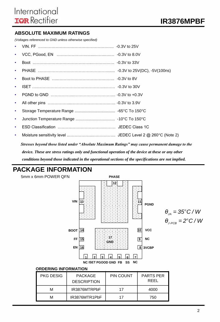
Block Diagram
PWM
GATE
DRIVE
LOGIC
ON-TIME+
-
SOFT
START
Run
+
CONTROL
LOGICPOR
+
-
VREF
x0.8
Zcross
VCC
FF
x1.2
UV#
SSDelay
Run
Run
3VCBP
VCC
VCC
SETSS
FB
PGOOD
VCC
BOOT
PHASE
PGND
FF
VIN
ISET
GND
EN
GND
PWM
COMP
+
-
VBG
LDO
GND
VCC
3VCBP
3VCBP
OVER
CURRENT
DCM
OC#
4
IR3876MPBF
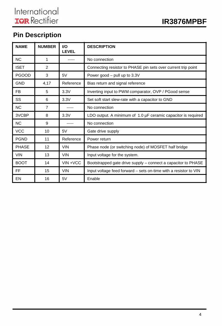
Pin Description
NAME NUMBER I/O
LEVEL
DESCRIPTION
NC 1 ----- No connection
ISET 2 Connecting resistor to PHASE pin sets over current trip point
PGOOD 3 5V Power good – pull up to 3.3V
GND 4,17 Reference Bias return and signal reference
FB 5 3.3V Inverting input to PWM comparator, OVP / PGood sense
SS 6 3.3V Set soft start slew-rate with a capacitor to GND
NC 7 ----- No connection
3VCBP 8 3.3V LDO output. A minimum of 1.0 µF ceramic capacitor is required
NC 9 ----- No connection
VCC 10 5V Gate drive supply
PGND 11 Reference Power return
PHASE 12 VIN Phase node (or switching node) of MOSFET half bridge
VIN 13 VIN Input voltage for the system.
BOOT 14 VIN +VCC Bootstrapped gate drive supply – connect a capacitor to PHASE
FF 15 VIN Input voltage feed forward – sets on-time with a resistor to VIN
EN 16 5V Enable
5
IR3876MPBF
Recommended Operating Conditions
Electrical Specifications Unless otherwise specified, these specification apply over VIN = 12V, VCC = 5V, 0oC ≤ TJ ≤ 125oC.
* Note: PHASE pin must not exceed 25V.
Symbol Definition Min Max Unit VIN Input Voltage 3 21*
V VCC Supply Voltage 4.5 7.5
VOUT Output Voltage 0.5 12
IOUT Output Current 0 12 A
Fs Switching Frequency N/A 1000 kHz
TJ Junction Temperature 0 125 oC
PARAMETER NOTE TEST CONDITION MIN TYP MAX UNIT
BIAS SUPPLIES
VCC Turn-on Threshold 3.9 4.2 4.5 V
VCC Turn-off Threshold 3.6 3.9 4.2 V
VCC Threshold Hysteresis 150 mV
VCC Operating Current RFF = 200K,
EN = HIGH, Fs = 300kHz
9.2 mA
VCC Shutdown Current EN = LOW 35 50 µA
FF Shutdown Current EN = LOW 2 µA
VIN Shutdown Current EN = LOW 1 µA
INTERNAL LDO OUTPUT
LDO Output Voltage Range CLDO = 1µF 3.1 3.3 3.5 V
Output Current 8 mA
CONTROL LOOP
Reference Accuracy, VREF VREF 0.495 0.5 0.505 V
On-Time Accuracy RFF = 180K, TJ = 65oC 280 300 320 ns
Min Off Time 1 400 ns
Soft-Start Current EN = HIGH 8 10 12 µA
Zero Current Threshold 1 Measure at VPHASE -5 -2.4 0 mV
FAULT PROTECTION
ISET Pin Output Current 18 20 22 µA
Under Voltage Threshold Falling VFB & Monitor PGOOD 0.37 0.4 0.43 V
Under Voltage Hysteresis 1 Rising VFB 10 mV
Over Voltage Threshold Rising VFB & Monitor PGOOD 0.58 0.62 0.66 V
Over Voltage Hysteresis 1 Falling VFB 10 mV
PGOOD Delay Threshold
(VSS)
1 V
6
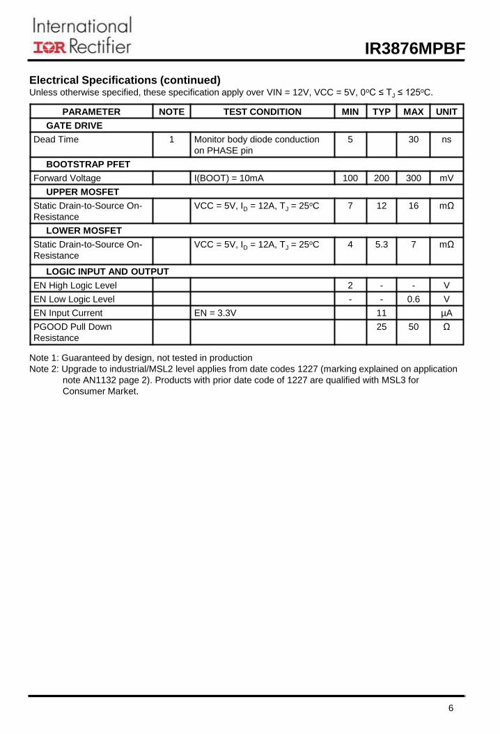
IR3876MPBF
Electrical Specifications (continued) Unless otherwise specified, these specification apply over VIN = 12V, VCC = 5V, 0oC ≤ TJ ≤ 125oC.
Note 1: Guaranteed by design, not tested in production
Note 2: Upgrade to industrial/MSL2 level applies from date codes 1227 (marking explained on application
note AN1132 page 2). Products with prior date code of 1227 are qualified with MSL3 for
Consumer Market.
PARAMETER NOTE TEST CONDITION MIN TYP MAX UNIT
GATE DRIVE
Dead Time 1 Monitor body diode conduction
on PHASE pin
5 30 ns
BOOTSTRAP PFET
Forward Voltage I(BOOT) = 10mA 100 200 300 mV
UPPER MOSFET
Static Drain-to-Source On-
Resistance
VCC = 5V, ID = 12A, TJ = 25oC 7 12 16 mΩ
LOWER MOSFET
Static Drain-to-Source On-
Resistance
VCC = 5V, ID = 12A, TJ = 25oC 4 5.3 7 mΩ
LOGIC INPUT AND OUTPUT
EN High Logic Level 2 - - V
EN Low Logic Level - - 0.6 V
EN Input Current EN = 3.3V 11 µA
PGOOD Pull Down
Resistance
25 50 Ω
7
IR3876MPBF
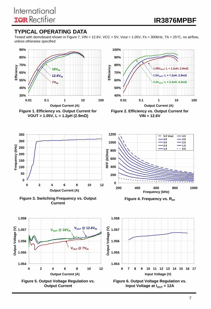
TYPICAL OPERATING DATA Tested with demoboard shown in Figure 7, VIN = 12.6V, VCC = 5V, Vout = 1.05V, Fs = 300kHz, TA = 25oC, no airflow,
unless otherwise specified
Figure 3. Switching Frequency vs. Output
Current
Figure 1. Efficiency vs. Output Current for
VOUT = 1.05V, L = 1.2µH (2.9mΩ)
Figure 2. Efficiency vs. Output Current for
VIN = 12.6V
Figure 4. Frequency vs. RFF
Figure 5. Output Voltage Regulation vs.
Output Current
Figure 6. Output Voltage Regulation vs.
Input Voltage at IOUT = 12A
0
50
100
150
200
250
300
350
0 2 4 6 8 10 12
Output Current (A)
Fre
qu
en
cy (
kH
z)
1.054
1.055
1.056
1.057
1.058
6 7 8 9 10 11 12 13 14 15 16 17
Input Voltage (V)
Ou
tpu
t V
olt
ag
e (
V)
1.054
1.055
1.056
1.057
1.058
0 2 4 6 8 10 12
Output Current (A)
Ou
tpu
t V
olt
ag
e (
V)
VOUT @ 16VINVOUT @ 12.6VIN
VOUT @ 7VIN
0
200
400
600
800
1000
1200
200 400 600 800 1000Frequency (kHz)
RF
F (
kO
hm
)
5.0 Vout 4.5
4.0 3.5
3.0 2.5
2.0 1.5
1.0 0.5
40%
50%
60%
70%
80%
90%
100%
0.01 0.1 1 10 100
Output Current (A)E
ffic
ien
cy
3.3VOUT; L = 2.2uH, 4.2mΩ
1.5VOUT; L = 1.2uH, 2.9mΩ
1.05VOUT; L = 1.2uH, 2.9mΩ
35%
45%
55%
65%
75%
85%
95%
0.01 0.1 1 10 100
Output Current (A)
Eff
icie
nc
y
16VIN
12.6VIN
7VIN
8
IR3876MPBF
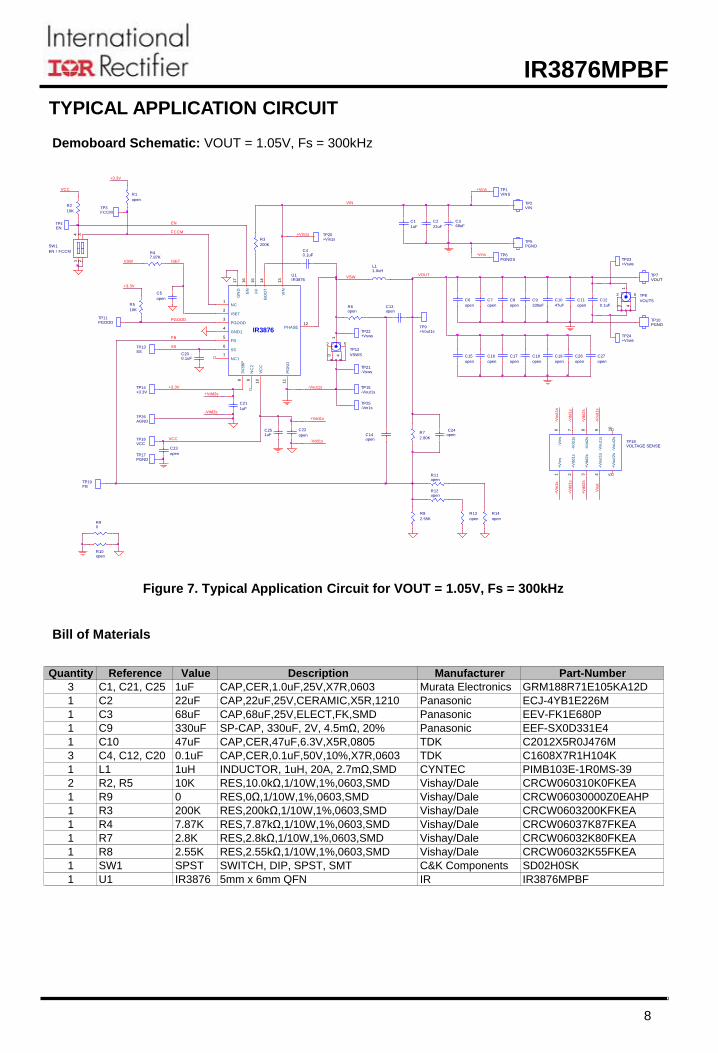
TYPICAL APPLICATION CIRCUIT
Demoboard Schematic: VOUT = 1.05V, Fs = 300kHz
Bill of Materials
Figure 7. Typical Application Circuit for VOUT = 1.05V, Fs = 300kHz
VOUT TP7
TP10
EN
R90
VCC
TP23+Vsws
TP24+Vsws
+Vins
R12open
C26
open
TP8
VOUTS
13 4
52
TP21-Vsws
TP25-Vin1s
C27
open
TP12
VSWS
13 4
52
TP22+Vsws
VIN
C7
open
C8
open
C9
330uF
C10
47uF
-Vout1
s
C11
open
-Vd
d2s
-Vd
d1s
C1
1uF
R7
2.80K
R8
2.55K
C12
0.1uF
PGOOD
C24open
ISET
-Vout1
s
+V
dd2s
Vout
+V
dd1s
+3.3V
+V
in1s
TP6PGNDS
TP14+3.3V
IR3876
U1IR3876
3V
3B
P8
NC1
SS6
PGOOD3
FF
15
GND14
FB5
GN
D17
NC17
ISET2
BO
OT
14
VIN
13
VC
C10
NC
29
PG
ND
11
PHASE12
EN
16
C40.1uF
VCC
TP4EN
SW1
EN / FCCM
1 24 3
TP17PGND
C200.1uF
TP26AGND
C5
open
VSW
C21
1uF
TP11PGOOD
L11.0uH
R6open
C22
open
TP1VINS
R47.87K
R3
200K
C13open
C2
22uF
C16
open
+ C368uF
TP2VIN
TP5PGND
C14open
C17
open
C18
open
TP16VCC
R10open
FB
R5
10K
C15
open
C6
open
TP18VOLTAGE SENSE
+V
ins
1
+V
dd1s
2
+V
dd2s
3
+V
out1
s4
+V
out2
s5
-Vout2
s10
-Vd
d2s
8
-Vout1
s9
-Vin
s6
-Vd
d1s
7
-Vout1s
TP9+Vout1s
R1
open
FCCM+Vin1s TP20
+Vin1s
+3.3V
C251uF
+Vdd1s
-Vdd1s
R13
open
+3.3V TP15-Vout1s
R14
open
TP19FB
R11open
TP13SS
VSW
+Vdd2s
TP3FCCM
SS
-Vdd2s
R2
10K
C19
open
-Vins
PGND
VOUT
C23
open
Quantity Reference Value Description Manufacturer Part-Number
3 C1, C21, C25 1uF CAP,CER,1.0uF,25V,X7R,0603 Murata Electronics GRM188R71E105KA12D
1 C2 22uF CAP,22uF,25V,CERAMIC,X5R,1210 Panasonic ECJ-4YB1E226M
1 C3 68uF CAP,68uF,25V,ELECT,FK,SMD Panasonic EEV-FK1E680P
1 C9 330uF SP-CAP, 330uF, 2V, 4.5mΩ, 20% Panasonic EEF-SX0D331E4
1 C10 47uF CAP,CER,47uF,6.3V,X5R,0805 TDK C2012X5R0J476M
3 C4, C12, C20 0.1uF CAP,CER,0.1uF,50V,10%,X7R,0603 TDK C1608X7R1H104K
1 L1 1uH INDUCTOR, 1uH, 20A, 2.7mΩ,SMD CYNTEC PIMB103E-1R0MS-39
2 R2, R5 10K RES,10.0kΩ,1/10W,1%,0603,SMD Vishay/Dale CRCW060310K0FKEA
1 R9 0 RES,0Ω,1/10W,1%,0603,SMD Vishay/Dale CRCW06030000Z0EAHP
1 R3 200K RES,200kΩ,1/10W,1%,0603,SMD Vishay/Dale CRCW0603200KFKEA
1 R4 7.87K RES,7.87kΩ,1/10W,1%,0603,SMD Vishay/Dale CRCW06037K87FKEA
1 R7 2.8K RES,2.8kΩ,1/10W,1%,0603,SMD Vishay/Dale CRCW06032K80FKEA
1 R8 2.55K RES,2.55kΩ,1/10W,1%,0603,SMD Vishay/Dale CRCW06032K55FKEA
1 SW1 SPST SWITCH, DIP, SPST, SMT C&K Components SD02H0SK
1 U1 IR3876 5mm x 6mm QFN IR IR3876MPBF
9
IR3876MPBF
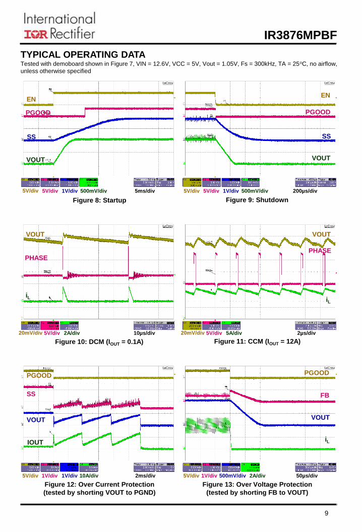
Figure 8: Startup Figure 9: Shutdown
Figure 10: DCM (IOUT = 0.1A) Figure 11: CCM (IOUT = 12A)
Figure 12: Over Current Protection
(tested by shorting VOUT to PGND)
Figure 13: Over Voltage Protection
(tested by shorting FB to VOUT)
EN
PGOOD
SS
VOUT
EN
PGOOD
SS
VOUT
VOUT
PHASE
iL
VOUT
PHASE
iL
PGOOD
VOUT
IOUT
PGOOD
FB
VOUT
iL
TYPICAL OPERATING DATA Tested with demoboard shown in Figure 7, VIN = 12.6V, VCC = 5V, Vout = 1.05V, Fs = 300kHz, TA = 25oC, no airflow,
unless otherwise specified
5V/div 5V/div 1V/div 500mV/div 5ms/div 5V/div 5V/div 1V/div 500mV/div 200µs/div
20mV/div 5V/div 2A/div 10µs/div 20mV/div 5V/div 5A/div 2µs/div
5V/div 1V/div 500mV/div 2A/div 50µs/div 5V/div 1V/div 1V/div 10A/div 2ms/div
SS
10
IR3876MPBF
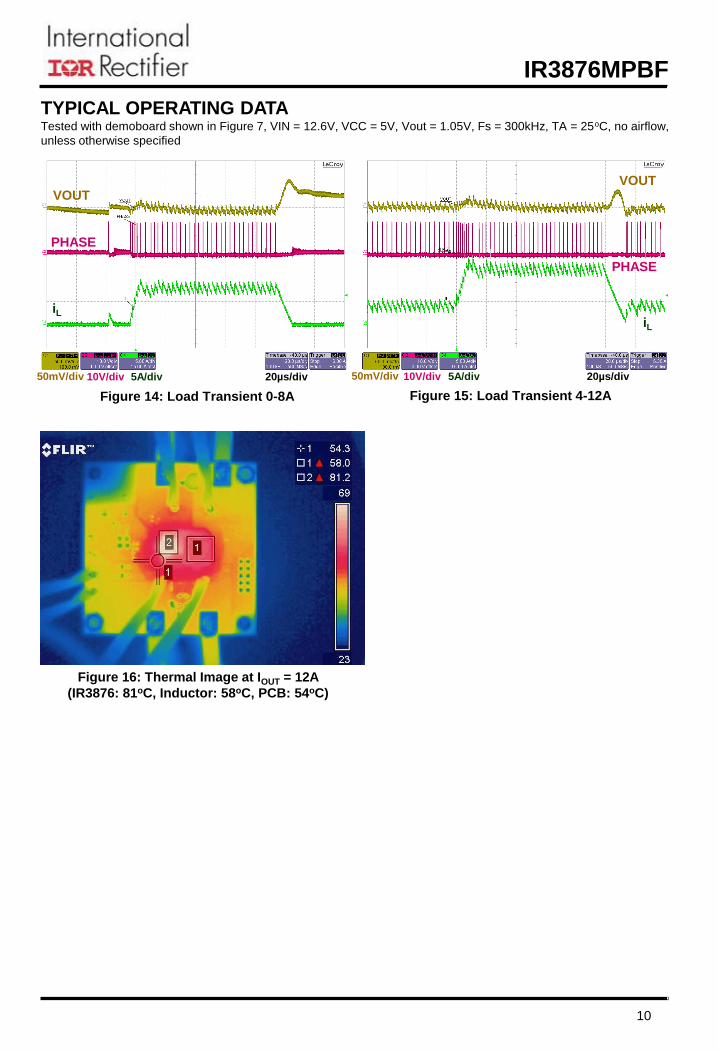
Figure 14: Load Transient 0-8A Figure 15: Load Transient 4-12A
Figure 16: Thermal Image at IOUT = 12A
(IR3876: 81oC, Inductor: 58oC, PCB: 54oC)
VOUT
PHASE
iL
VOUT
PHASE
iL
50mV/div 10V/div 5A/div 20µs/div 50mV/div 10V/div 5A/div 20µs/div
TYPICAL OPERATING DATA Tested with demoboard shown in Figure 7, VIN = 12.6V, VCC = 5V, Vout = 1.05V, Fs = 300kHz, TA = 25oC, no airflow,
unless otherwise specified
11
IR3876MPBF
PWM COMPARATOR
The PWM comparator initiates a SET signal
(PWM pulse) when the FB pin falls below the
reference (Vref) or the soft start (SS) voltage.
ON-TIME GENERATOR
The PWM on-time duration is programmed with
an external resistor (RFF) from the input supply
(VIN) to the FF pin. The simplified calculation for
RFF is shown in equation 1. The FF pin is held to
an internal reference after EN goes HIGH. A copy
of the current in RFF charges a timing capacitor,
which sets the on-time duration, as shown in
equation 2.
CONTROL LOGIC
The control logic monitors input power sources,
sequences the converter through the soft-start
and protective modes, and initiates an internal
RUN signal when all conditions are met.
VCC and 3VCBP pins are continuously monitored,
and the IR3876 will be disabled if the voltage of
either pin drops below the falling thresholds.
EN_DELAY will become HIGH when VCC and
3VCBP are in the normal operating range and the
EN pin = HIGH.
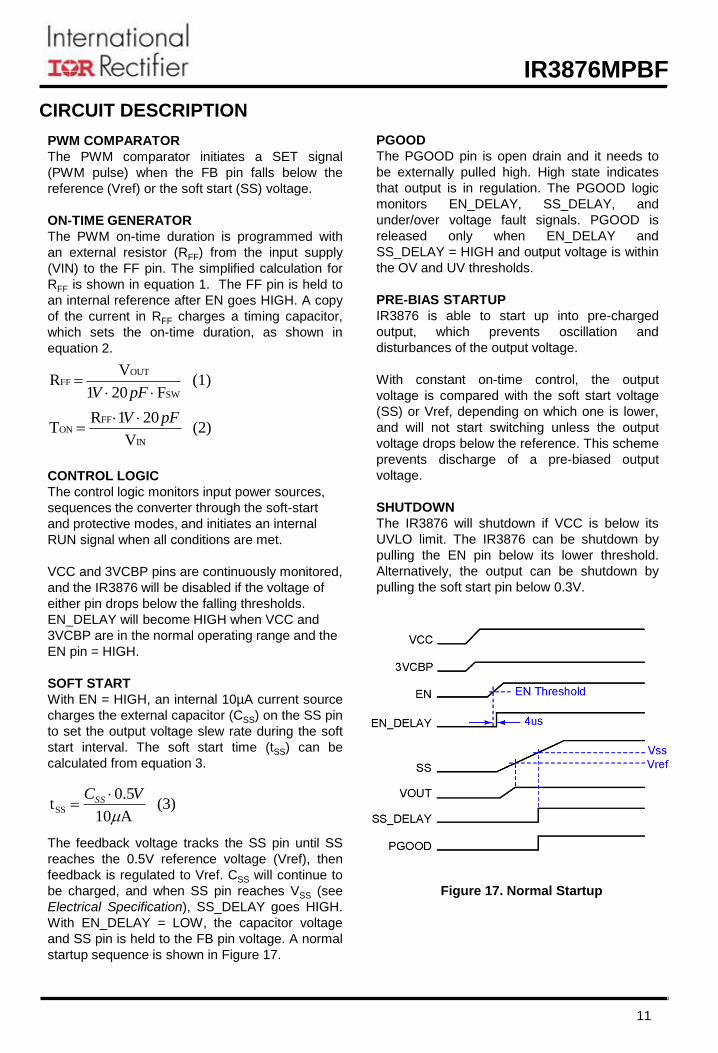
SOFT START
With EN = HIGH, an internal 10µA current source
charges the external capacitor (CSS) on the SS pin
to set the output voltage slew rate during the soft
start interval. The soft start time (tSS) can be
calculated from equation 3.
The feedback voltage tracks the SS pin until SS
reaches the 0.5V reference voltage (Vref), then
feedback is regulated to Vref. CSS will continue to
be charged, and when SS pin reaches VSS (see
Electrical Specification), SS_DELAY goes HIGH.
With EN_DELAY = LOW, the capacitor voltage
and SS pin is held to the FB pin voltage. A normal
startup sequence is shown in Figure 17.
CIRCUIT DESCRIPTION
(2) V
201RT
IN
FFON
pFV
(1) F201
VR
SW
OUTFF
pFV
(3) A10
5.0tSS
VCSS
Figure 17. Normal Startup
PGOOD
The PGOOD pin is open drain and it needs to
be externally pulled high. High state indicates
that output is in regulation. The PGOOD logic
monitors EN_DELAY, SS_DELAY, and
under/over voltage fault signals. PGOOD is
released only when EN_DELAY and
SS_DELAY = HIGH and output voltage is within
the OV and UV thresholds.
PRE-BIAS STARTUP
IR3876 is able to start up into pre-charged
output, which prevents oscillation and
disturbances of the output voltage.
With constant on-time control, the output
voltage is compared with the soft start voltage
(SS) or Vref, depending on which one is lower,
and will not start switching unless the output
voltage drops below the reference. This scheme
prevents discharge of a pre-biased output
voltage.
SHUTDOWN
The IR3876 will shutdown if VCC is below its
UVLO limit. The IR3876 can be shutdown by
pulling the EN pin below its lower threshold.
Alternatively, the output can be shutdown by
pulling the soft start pin below 0.3V.
12
IR3876MPBF
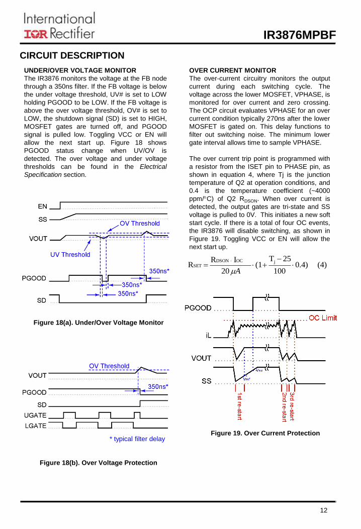
UNDER/OVER VOLTAGE MONITOR
The IR3876 monitors the voltage at the FB node
through a 350ns filter. If the FB voltage is below
the under voltage threshold, UV# is set to LOW
holding PGOOD to be LOW. If the FB voltage is
above the over voltage threshold, OV# is set to
LOW, the shutdown signal (SD) is set to HIGH,
MOSFET gates are turned off, and PGOOD
signal is pulled low. Toggling VCC or EN will
allow the next start up. Figure 18 shows
PGOOD status change when UV/OV is
detected. The over voltage and under voltage
thresholds can be found in the Electrical
Specification section.
CIRCUIT DESCRIPTION
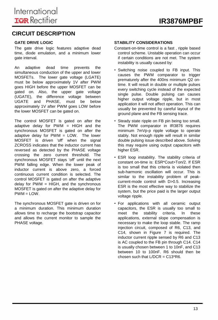
OVER CURRENT MONITOR
The over-current circuitry monitors the output
current during each switching cycle. The
voltage across the lower MOSFET, VPHASE, is
monitored for over current and zero crossing.
The OCP circuit evaluates VPHASE for an over
current condition typically 270ns after the lower
MOSFET is gated on. This delay functions to
filter out switching noise. The minimum lower
gate interval allows time to sample VPHASE.
The over current trip point is programmed with
a resistor from the ISET pin to PHASE pin, as
shown in equation 4, where Tj is the junction
temperature of Q2 at operation conditions, and
0.4 is the temperature coefficient (~4000
ppm/C) of Q2 RDSON. When over current is
detected, the output gates are tri-state and SS
voltage is pulled to 0V. This initiates a new soft
start cycle. If there is a total of four OC events,
the IR3876 will disable switching, as shown in
Figure 19. Toggling VCC or EN will allow the
next start up.
(4) 0.4)100
25T(1
20
IRR
jOC DSONSET
A
Figure 19. Over Current Protection
Figure 18(a). Under/Over Voltage Monitor
Figure 18(b). Over Voltage Protection
* typical filter delay
13
IR3876MPBF
CIRCUIT DESCRIPTION
STABILITY CONSIDERATIONS
Constant-on-time control is a fast , ripple based
control scheme. Unstable operation can occur
if certain conditions are not met. The system
instability is usually caused by:
• Switching noise coupled to FB input. This
causes the PWM comparator to trigger
prematurely after the 400ns minimum Q2 on-
time. It will result in double or multiple pulses
every switching cycle instead of the expected
single pulse. Double pulsing can causes
higher output voltage ripple, but in most
application it will not affect operation. This can
usually be prevented by careful layout of the
ground plane and the FB sensing trace.
• Steady state ripple on FB pin being too small.
The PWM comparator in IR3876 requires
minimum 7mVp-p ripple voltage to operate
stably. Not enough ripple will result in similar
double pulsing issue described above. Solving
this may require using output capacitors with
higher ESR.
• ESR loop instability. The stability criteria of
constant on-time is: ESR*Cout>Ton/2. If ESR
is too small that this criteria is violated then
sub-harmonic oscillation will occur. This is
similar to the instability problem of peak-
current-mode control with D>0.5. Increasing
ESR is the most effective way to stabilize the
system, but the price paid is the larger output
voltage ripple.
• For applications with all ceramic output
capacitors, the ESR is usually too small to
meet the stability criteria. In these
applications, external slope compensation is
necessary to make the loop stable. The ramp
injection circuit, composed of R6, C13, and
C14, shown in Figure 7 is required. The
inductor current ripple sensed by R6 and C13
is AC coupled to the FB pin through C14. C14
is usually chosen between 1 to 10nF, and C13
between 10 to 100nF. R6 should then be
chosen such that L/DCR = C13*R6.
GATE DRIVE LOGIC
The gate drive logic features adaptive dead
time, diode emulation, and a minimum lower
gate interval.
An adaptive dead time prevents the
simultaneous conduction of the upper and lower
MOSFETs. The lower gate voltage (LGATE)
must be below approximately 1V after PWM
goes HIGH before the upper MOSFET can be
gated on. Also, the upper gate voltage
(UGATE), the difference voltage between
UGATE and PHASE, must be below
approximately 1V after PWM goes LOW before
the lower MOSFET can be gated on.
The control MOSFET is gated on after the
adaptive delay for PWM = HIGH and the
synchronous MOSFET is gated on after the
adaptive delay for PWM = LOW. The lower
MOSFET is driven ‘off’ when the signal
ZCROSS indicates that the inductor current has
reversed as detected by the PHASE voltage
crossing the zero current threshold. The
synchronous MOSFET stays ‘off’ until the next
PWM falling edge. When the lower peak of
inductor current is above zero, a forced
continuous current condition is selected. The
control MOSFET is gated on after the adaptive
delay for PWM = HIGH, and the synchronous
MOSFET is gated on after the adaptive delay for
PWM = LOW.
The synchronous MOSFET gate is driven on for
a minimum duration. This minimum duration
allows time to recharge the bootstrap capacitor
and allows the current monitor to sample the
PHASE voltage.
14
IR3876MPBF
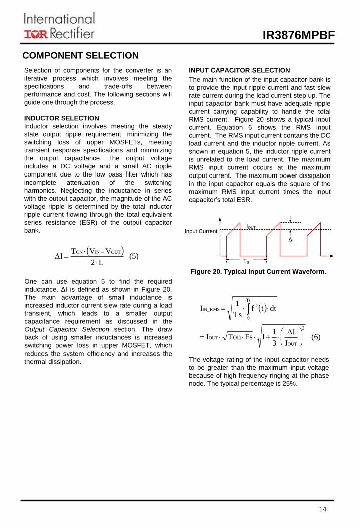
INPUT CAPACITOR SELECTION
The main function of the input capacitor bank is
to provide the input ripple current and fast slew
rate current during the load current step up. The
input capacitor bank must have adequate ripple
current carrying capability to handle the total
RMS current. Figure 20 shows a typical input
current. Equation 6 shows the RMS input
current. The RMS input current contains the DC
load current and the inductor ripple current. As
shown in equation 5, the inductor ripple current
is unrelated to the load current. The maximum
RMS input current occurs at the maximum
output current. The maximum power dissipation
in the input capacitor equals the square of the
maximum RMS input current times the input
capacitor’s total ESR.
Figure 20. Typical Input Current Waveform.
COMPONENT SELECTION
Selection of components for the converter is an
iterative process which involves meeting the
specifications and trade-offs between
performance and cost. The following sections will
guide one through the process.
INDUCTOR SELECTION
Inductor selection involves meeting the steady
state output ripple requirement, minimizing the
switching loss of upper MOSFETs, meeting
transient response specifications and minimizing
the output capacitance. The output voltage
includes a DC voltage and a small AC ripple
component due to the low pass filter which has
incomplete attenuation of the switching
harmonics. Neglecting the inductance in series
with the output capacitor, the magnitude of the AC
voltage ripple is determined by the total inductor
ripple current flowing through the total equivalent
series resistance (ESR) of the output capacitor
bank.
(5)
L2
VVTΔI
OUTINON
Input Current
ΔI
IOUT
TS
(6) I
ΔI
3
11FsTonI
dttfTs
1I
2
OUT
OUT
Ts
0
2IN_RMS
The voltage rating of the input capacitor needs
to be greater than the maximum input voltage
because of high frequency ringing at the phase
node. The typical percentage is 25%.
One can use equation 5 to find the required
inductance. ΔI is defined as shown in Figure 20.
The main advantage of small inductance is
increased inductor current slew rate during a load
transient, which leads to a smaller output
capacitance requirement as discussed in the
Output Capacitor Selection section. The draw
back of using smaller inductances is increased
switching power loss in upper MOSFET, which
reduces the system efficiency and increases the
thermal dissipation.
15
IR3876MPBF
BOOT CAPACITOR SELECTION
The boot capacitor starts the cycle fully charged
to a voltage of VB(0). Cg equals 0.65nF in
IR3876. Choose a sufficiently small ΔV such
that VB(0)-ΔV exceeds the maximum gate
threshold voltage to turn on the high side
MOSFET.
Choose a boot capacitor value larger than the
calculated CBOOT in equation 9. Equation 9 is
based on charge balance at CCM operation.
Usually the boot capacitor will be discharged to
a much lower voltage when the circuit is
operating in DCM mode at light load, due to
much longer Q2 off time and the bias current
drawn by the IC. Boot capacitance needs to be
increased if insufficient turn-on of Q1 is
observed at light load, typically larger than
0.1µF is needed. The voltage rating of this part
needs to be larger than VB(0) plus the desired
derating voltage. Its ESR and ESL needs to be
low in order to allow it to deliver the large
current and di/dt’s which drive MOSFETs most
efficiently. In support of these requirements a
ceramic capacitor should be chosen.
OUTPUT CAPACITOR SELECTION
Selection of the output capacitor requires meeting
voltage overshoot requirements during load
removal, and meeting steady state output ripple
voltage requirements. The output capacitor is the
most expensive converter component and
increases the overall system cost. The output
capacitor decoupling in the converter typically
includes the low frequency capacitor, such as
Specialty Polymer Aluminum, and mid frequency
ceramic capacitors.
The first purpose of output capacitors is to provide
current when the load demand exceeds the
inductor current, as shown in Figure 21. Equation
7 shows the charge requirement for a certain load.
The advantage provided by the IR3876 at a load
step is to reduce the delay compared to a fixed
frequency control method (in microseconds or (1-
D)*Ts). If the load increases right after the PWM
signal goes low, the longest delay will be equal to
the minimum lower gate on as shown in the
Electrical Specification table. The IR3876 also
reduces the inductor current slew time, the time it
takes for the inductor current to reach equality
with the output current, by increasing the
switching frequency up to 2.5MHz. The result
reduces the recovery time.
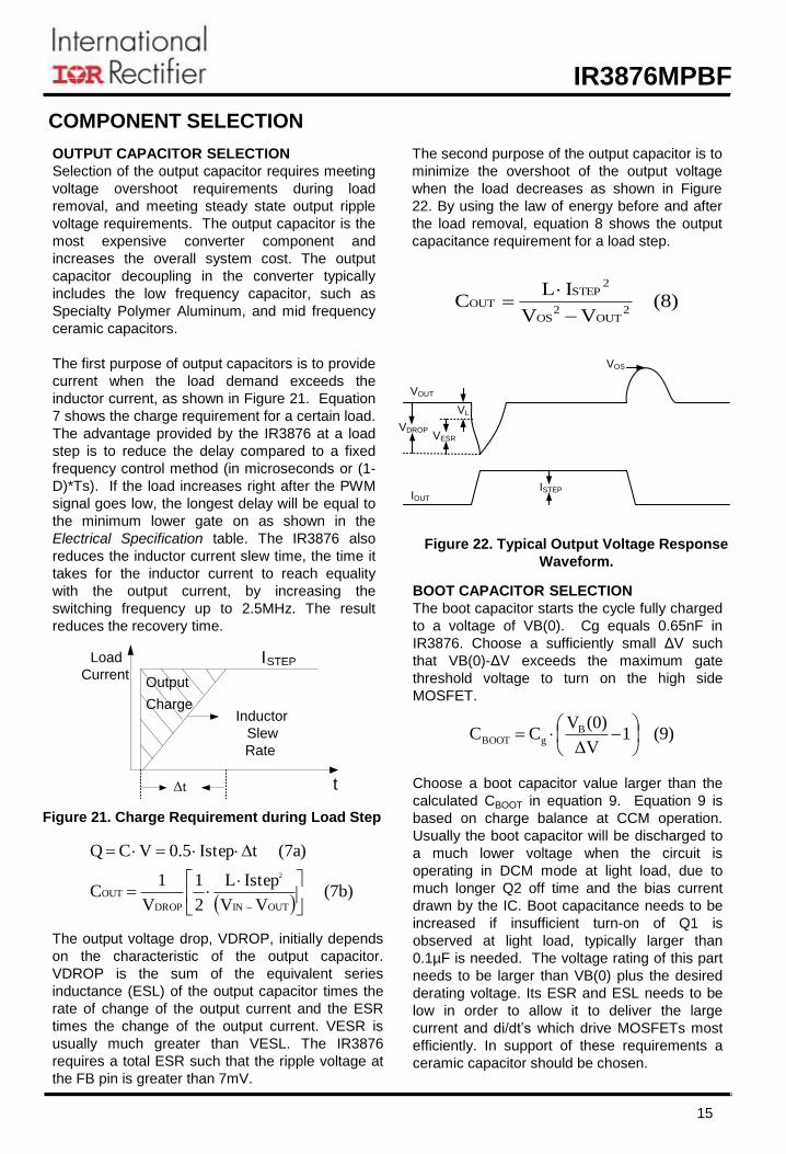
The second purpose of the output capacitor is to
minimize the overshoot of the output voltage
when the load decreases as shown in Figure
22. By using the law of energy before and after
the load removal, equation 8 shows the output
capacitance requirement for a load step.
Figure 21. Charge Requirement during Load Step
(7b)
VV
IstepL
2
1
V
1C
(7a)t Istep0.5VC Q
OUTINDROP
OUT
2
The output voltage drop, VDROP, initially depends
on the characteristic of the output capacitor.
VDROP is the sum of the equivalent series
inductance (ESL) of the output capacitor times the
rate of change of the output current and the ESR
times the change of the output current. VESR is
usually much greater than VESL. The IR3876
requires a total ESR such that the ripple voltage at
the FB pin is greater than 7mV.
t
Load
CurrentISTEP
Inductor
Slew
Rate
Output
Charge
Δt
(8) VV
IL C
2OUT
2OS
2STEP
OUT
IOUT
ISTEP
VOUT
VL
VESR
VOS
VDROP
Figure 22. Typical Output Voltage Response
Waveform.
(9) 1ΔV
(0)VCC B
gBOOT
COMPONENT SELECTION
16
IR3876MPBF
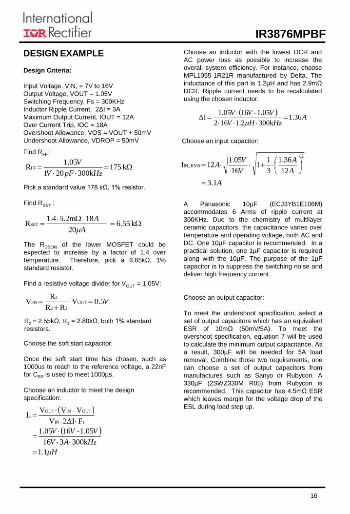
DESIGN EXAMPLE
Design Criteria:
Input Voltage, VIN, = 7V to 16V
Output Voltage, VOUT = 1.05V
Switching Frequency, Fs = 300KHz
Inductor Ripple Current, 2ΔI = 3A
Maximum Output Current, IOUT = 12A
Over Current Trip, IOC = 18A
Overshoot Allowance, VOS = VOUT + 50mV
Undershoot Allowance, VDROP = 50mV Choose an input capacitor:
Find RFF :
Choose an inductor with the lowest DCR and
AC power loss as possible to increase the
overall system efficiency. For instance, choose
MPL1055-1R21R manufactured by Delta. The
inductance of this part is 1.2µH and has 2.9mΩ
DCR. Ripple current needs to be recalculated
using the chosen inductor.
A
A
A
V
VA
3.1
21
36.1
3
11
16
1.0521I
2
IN_RMS
A Panasonic 10µF (ECJ3YB1E106M)
accommodates 6 Arms of ripple current at
300KHz. Due to the chemistry of multilayer
ceramic capacitors, the capacitance varies over
temperature and operating voltage, both AC and
DC. One 10µF capacitor is recommended. In a
practical solution, one 1µF capacitor is required
along with the 10µF. The purpose of the 1µF
capacitor is to suppress the switching noise and
deliver high frequency current.
Choose an output capacitor:
To meet the undershoot specification, select a
set of output capacitors which has an equivalent
ESR of 10mΩ (50mV/5A). To meet the
overshoot specification, equation 7 will be used
to calculate the minimum output capacitance. As
a result, 300µF will be needed for 5A load
removal. Combine those two requirements, one
can choose a set of output capacitors from
manufactures such as Sanyo or Rubycon. A
330µF (2SWZ330M R05) from Rubycon is
recommended. This capacitor has 4.5mΩ ESR
which leaves margin for the voltage drop of the
ESL during load step up.
k 175 300k201
1.05RFF
HzpFV
V
Pick a standard value 178 kΩ, 1% resistor.
Find RSET :
k 6.55 20
18 m2.51.4R
SET
A
A
H
HzAV
VVV
1.1
300k361
1.05-611.05
FΔI2V
VVVL
sIN
OUTINOUT
A
HzHV
VVV1.36
300k2.1612
1.05-611.05ΔI
The RDSON of the lower MOSFET could be
expected to increase by a factor of 1.4 over
temperature. Therefore, pick a 6.65kΩ, 1%
standard resistor.
Find a resistive voltage divider for VOUT = 1.05V:
Choose the soft start capacitor:
Once the soft start time has chosen, such as
1000us to reach to the reference voltage, a 22nF
for CSS is used to meet 1000µs.
Choose an inductor to meet the design
specification:
V0.5 V RR
RV OUT
12
2FB
R2 = 2.55kΩ, R1 = 2.80kΩ, both 1% standard
resistors.

17
IR3876MPBF
Bypass Capacitor:
One 1µF high quality ceramic capacitor should be
placed as near VCC pin as possible. The other
end of capacitor can be connected to a via or
connected directly to GND plane. Use a GND
plane instead of a thin trace to the GND pin
because a thin trace have too much impedance.
Boot Circuit:
CBOOT should be placed near the BOOT and
PHASE pins to reduce the impedance when the
upper MOSFET turns on.
Power Stage:
Figure 23 shows the current paths and their
directions for the on and off periods. The on time
path has low average DC current and high AC
current. Therefore, it is recommended to place the
input ceramic capacitor, upper, and lower
MOSFET in a tight loop as shown in Figure 23.
The purpose of the tight loop from the input
ceramic capacitor is to suppress the high
frequency (10MHz range) switching noise and
reduce Electromagnetic Interference (EMI). If this
path has high inductance, the circuit will cause
voltage spikes and ringing, and increase the
switching loss. The off time path has low AC and
high average DC current. Therefore, it should be
laid out with a tight loop and wide trace at both
ends of the inductor. Lowering the loop resistance
reduces the power loss. The typical resistance
value of 1-ounce copper thickness is 0.5mΩ per
square inch.
Figure 23. Current Path of Power Stage
LAYOUT RECOMMENDATION
Q1
Q2
V OUT
V IN
ON
OFF
C OUT
C IN
IR 3876
18
IR3876MPBF
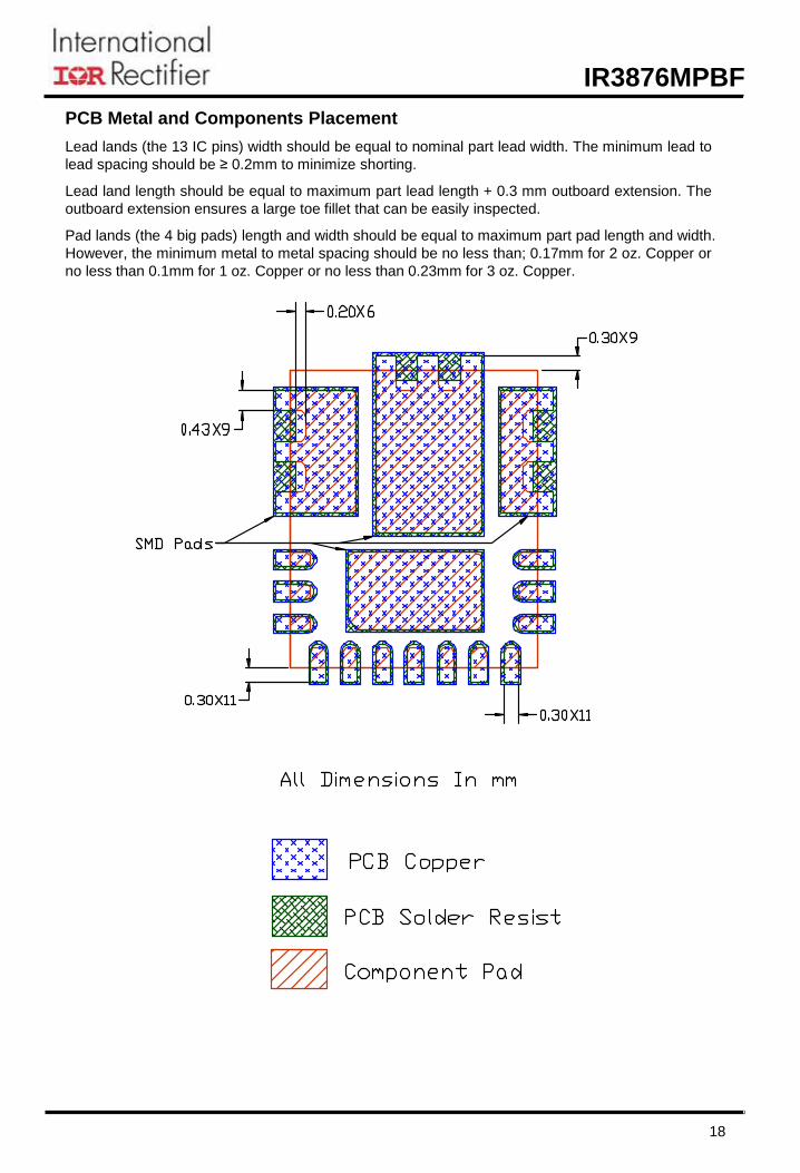
PCB Metal and Components Placement
Lead lands (the 13 IC pins) width should be equal to nominal part lead width. The minimum lead to
lead spacing should be ≥ 0.2mm to minimize shorting.
Lead land length should be equal to maximum part lead length + 0.3 mm outboard extension. The
outboard extension ensures a large toe fillet that can be easily inspected.
Pad lands (the 4 big pads) length and width should be equal to maximum part pad length and width.
However, the minimum metal to metal spacing should be no less than; 0.17mm for 2 oz. Copper or
no less than 0.1mm for 1 oz. Copper or no less than 0.23mm for 3 oz. Copper.
19
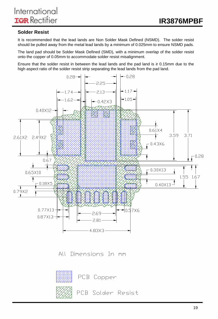
IR3876MPBF
Solder Resist
It is recommended that the lead lands are Non Solder Mask Defined (NSMD). The solder resist
should be pulled away from the metal lead lands by a minimum of 0.025mm to ensure NSMD pads.
The land pad should be Solder Mask Defined (SMD), with a minimum overlap of the solder resist
onto the copper of 0.05mm to accommodate solder resist misalignment.
Ensure that the solder resist in between the lead lands and the pad land is ≥ 0.15mm due to the
high aspect ratio of the solder resist strip separating the lead lands from the pad land.
20
IR3876MPBF
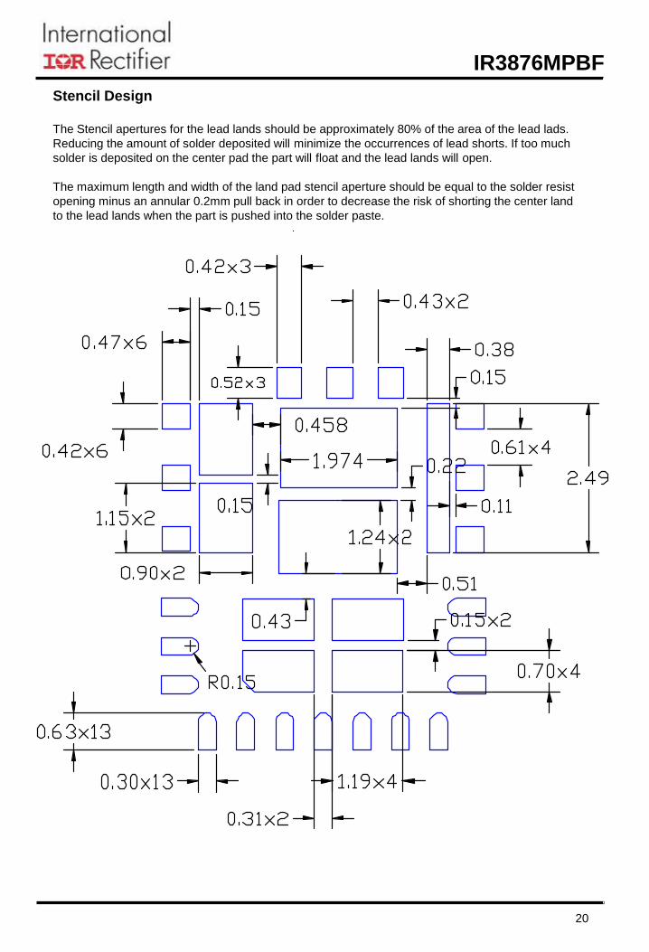
Stencil Design
The Stencil apertures for the lead lands should be approximately 80% of the area of the lead lads.
Reducing the amount of solder deposited will minimize the occurrences of lead shorts. If too much
solder is deposited on the center pad the part will float and the lead lands will open.
The maximum length and width of the land pad stencil aperture should be equal to the solder resist
opening minus an annular 0.2mm pull back in order to decrease the risk of shorting the center land
to the lead lands when the part is pushed into the solder paste.
21
IR3876MPBF
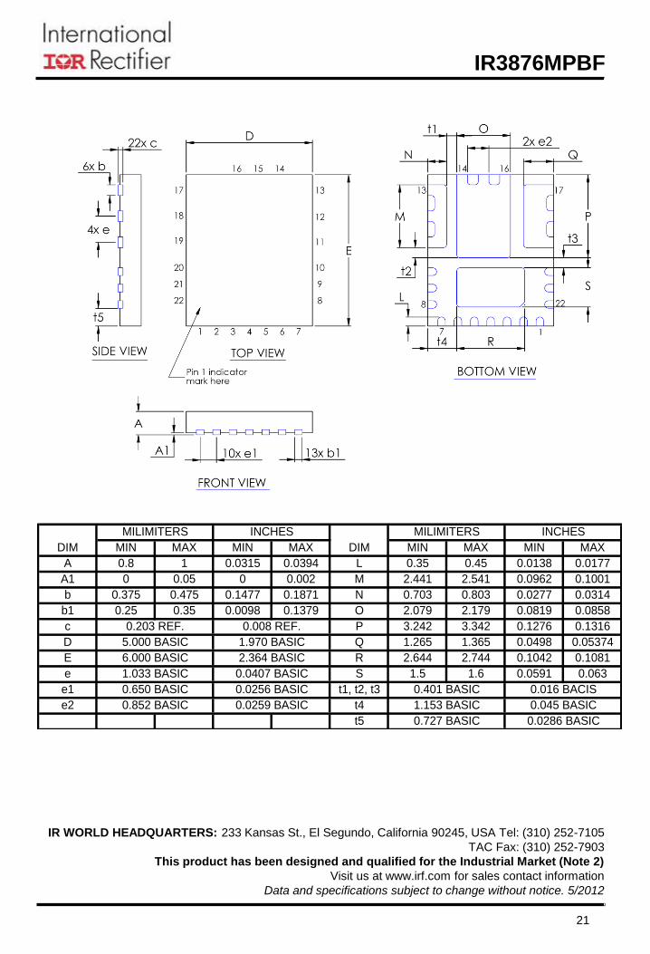
MIN MAX MIN MAX MIN MAX MIN MAX
A 0.8 1 0.0315 0.0394 L 0.35 0.45 0.0138 0.0177
A1 0 0.05 0 0.002 M 2.441 2.541 0.0962 0.1001
b 0.375 0.475 0.1477 0.1871 N 0.703 0.803 0.0277 0.0314
b1 0.25 0.35 0.0098 0.1379 O 2.079 2.179 0.0819 0.0858
c P 3.242 3.342 0.1276 0.1316
D Q 1.265 1.365 0.0498 0.05374
E R 2.644 2.744 0.1042 0.1081
e S 1.5 1.6 0.0591 0.063
e1 t1, t2, t3
e2 t4
t5
DIM
MILIMITERS INCHES
DIM
MILIMITERS INCHES
0.203 REF. 0.008 REF.
5.000 BASIC 1.970 BASIC
6.000 BASIC 2.364 BASIC
1.033 BASIC 0.0407 BASIC
0.650 BASIC 0.0256 BASIC
0.852 BASIC 0.0259 BASIC 1.153 BASIC 0.045 BASIC
0.727 BASIC 0.0286 BASIC
0.401 BASIC 0.016 BACIS
IR WORLD HEADQUARTERS: 233 Kansas St., El Segundo, California 90245, USA Tel: (310) 252-7105
TAC Fax: (310) 252-7903
This product has been designed and qualified for the Industrial Market (Note 2)
Visit us at www.irf.com for sales contact information
Data and specifications subject to change without notice. 5/2012