Embed Size (px)
Citation preview
SPRAAI4A– September 2009 Submit Documentation Feedback
Booting and Flashing via the DaVinci TMS320DM644x Serial Interface 1
Copyright © 2009, Texas Instruments Incorporated
Application Report SPRAAI4A– September 2009
Booting and Flashing via the DaVinci TMS320DM644x Serial Interface
Daniel J. Allred
ABSTRACT This application report describes two related pieces of software that are used together to boot the ARM core of the DM644x via the universal asynchronous receiver/transmitter (UART0) serial interface. Additionally, this software allows you to write the needed files to a NAND or NOR flash device, connected to the DM644x AEMIF, such that the ARM core can boot from these external memories. The software consists of a host application, which runs on your PC, and a user boot loader (UBL), which runs on the DM644x ARM core. This UBL also can be placed in the NAND flash memory to enable booting from this device. The software presented in this application report is an extension of that discussed in Basic Application Loading over the Serial Interface for the DaVinci TMS320DM644x (SPRAAI0). This application report contains project code that can be downloaded from http://www.ti.com/lit/zip/SPRAAI4.
NOTE: The associated software described by this document is no longer supported and is meant for informational and archival purposes. The information contained in this document regarding the boot processes of the DM644x device itself is still correct and accurate. Details about updated software tools can be found at the following URL: http://wiki.davincidsp.com/index.php?title=Serial_Boot_and_Flash_Loading_Utility.
Contents 1 TMS320DM644x Boot Overview .......................................................................................................................... 2 2 Target Application Used as a UBL ....................................................................................................................... 3 3 Target Application to Write to NAND or NOR Flash in UART-Boot Mode ............................................................ 9 4 Host Application ................................................................................................................................................. 12 5 References......................................................................................................................................................... 15 Appendix A UART-Boot Mode Flash Command Code .............................................................................................. 16 Appendix B Self-Copy Code for NOR UBL ................................................................................................................ 18 Appendix C Supported NOR Devices and Configurations ......................................................................................... 19 Appendix D Supported NAND Devices ...................................................................................................................... 20 Appendix E NAND ECC Considerations .................................................................................................................... 21
List of Figures 1 ROM Boot Loader NAND Mode Program Flow ................................................................................................... 5 2 General Host Program Flow .............................................................................................................................. 13
List of Tables 1 Boot Modes for DM644x Device .......................................................................................................................... 3 2 Overview of UBL Source Code Files and Structure ............................................................................................. 4 3 NAND UBL Header .............................................................................................................................................. 6 4 NAND Application Header ................................................................................................................................... 6 5 NAND vs NOR Flash Comparison ....................................................................................................................... 7 6 NOR Application Header ...................................................................................................................................... 8

TMS320DM644x Boot Overview www.ti.com
Copyright © 2009, Texas Instruments Incorporated
7 Table of Acceptable NAND Commands for Use in NAND UBL UART-Boot Mode .............................................. 9 8 NAND Application Image Header Magic Number ............................................................................................... 10 9 Table of Acceptable NOR Commands for Use in NOR UBL UART-Boot Mode................................................. 11 10 UBL/Host Interfacing Sequences ....................................................................................................................... 14 11 NOR Configurations Supported by the nor.c Driver ........................................................................................... 19 12 NAND Devices Supported by the nand.c Driver ................................................................................................. 20 2 ECC Value Location in Spare Page Bytes of 256-Byte/Page NAND Devices .................................................... 21 2 ECC Value Location in Spare Page Bytes of 512-Byte/Page NAND Devices .................................................... 21 2 ECC Value Location in Spare Page Bytes of 2048-Byte/Page NAND Devices .................................................. 21
1 TMS320DM644x Boot Overview This section gives an overview of the boot process of the DM644x device. This section mirrors the presentation given in the Chapter 12 of the TMS320DM644x DMSoC ARM Subsystem Reference Guide (SPRUE14). The reader should be familiar with all the information in that chapter before proceeding. Additional details can be found in the boot mode section of the TMS320DM6446 Digital Media System-on-Chip data manual (SPRS283). Upon reset or power up, the DM644x begins executing code from its ROM boot loader (RBL). The RBL determines how to boot based on the logic levels at pins BTSEL[1..0]. These values are latched into the BOOTCFG register bits 7..6 at reset, and the RBL reads this register to determine the intended boot mode. On the Spectrum Digital DVEVM board, these pins are attached to switches S3-2 and S3-1, respectively, allowing you to change the intended boot mode while the board is powered off. Table 1 shows the available boot modes for the DM644x. In this application report, particular attention is paid to the UART-boot mode. This mode is unique in that it generally requires a connection to an external host system in order to function. The traditional intention is that a secondary boot loader, referred to as a User Boot Loader (UBL) in the TMS320DM644x DMSoC ARM Subsystem Reference Guide (SPRUE14), would be downloaded by the RBL. This UBL would then be used to initialize certain subsystems of the chip, such as the DDR2 memory controller, and download a tertiary boot loader or application. An example would be the u-boot boot loader, which has been written with the objective of loading the Linux®kernel onto embedded systems. In the NAND-boot mode, the RBL requires a similar UBL to exist in the NAND memory to load the tertiary boot loader or application from NAND to RAM. The NOR-boot mode can use a UBL, though it is not required. Details of how the UBL is structured and used are given in Section 2.
Linux is a registered trademark of Linus Torvalds in the U.S. and other countries. Microsoft, Microsoft Windows are registered trademarks of Microsoft Corporation in the United States and/or other countries. Novell is a registered trademark of Novell, Inc. in the United States and other countries. All other trademarks are the property of their respective owners.
2 Booting and Flashing via the DaVinci TMS320DM644x Serial Interface SPRAAI4A– September 2009 Submit Documentation Feedback

Copyright © 2009, Texas Instruments Incorporated
Target Application Used as a UBL www.ti.com
Table 1. Boot Modes for DM644x Device
BTSEL0 (DVEVM SW3-1) BTSEL1 (DVEVM SW3-2) Boot Mode 0 0 NAND Flash Boot 1 0 NOR Flash Boot 0 1 Reserved 1 1 UART Boot
The presence of the attached host in the UART-boot mode allows you to do more than simply load additional executable code. With a properly written host and target application (i.e., the UBL), a number of low-level system functions can be executed. This application report describes the development of a target application that can act as a UBL for all three boot modes, and provides additional means, while in the UART-boot mode, to prepare the NAND or NOR flash devices for booting. This document also provides details of the host application that interfaces with the UBL over the serial link. Emphasis is placed on how these two pieces of software must be developed jointly. Details of the UBL's use as a flashing application are given in Section 3. Details of the host application can be found in Section 4. The reader should note that the UBL and host application presented here are more complex extensions of the target and host applications described in the Basic Application Loading Over the Serial Interface for the DaVinci TMS320DM644x (SPRAAI0).
2 Target Application Used as a UBL
The target application is the binary executable that is downloaded via the UART during the UART boot process, i.e., the UART UBL. This UBL is downloaded to the ARM internal memory. Once located there, the UBL is verified and begins execution. The UBL is then responsible for initializing the system to a desired state. Usually this will involve turning on the DDR memory interface and setting the system clock. See the dm644x.c file and SPRAAI0 for more details. The target application presented in this document has been written so that it also can be used as a boot loader for the NAND- and NOR-boot modes, as well as the UART-boot mode. Consequently, the terms 'target application' and 'UBL' are used interchangeably for the remainder of the document. In this section, the discussion focuses on how the UBL code is written to act as a boot loader (i.e., downloading and executing an application or tertiary boot loader) for the three possible boot modes. Section 2.1 presents the overall structure of the code files that make up the UBL and their role in the various boot modes. Section 2.2 to Section 2.4 give details of each of the boot modes and the use of the UBL in these modes.
2.1 General Description of UBL Code
The source code for the UBL, found in the ubl/src directory, is divided logically into files by boot mode and function, with the exception of three general files. The filenames and their descriptions are shown in Table 2. The file dm644x.c contains the necessary system initialization procedures, such as those described in SPRAAI0 (the code is nearly identical). The file util.c contains some miscellaneous code used to allocate memory from the initialized RAM space, provide wait loops throughout the UBL, and decode Motorola S-record images downloaded over the UART or loaded out of flash memory. The file ubl.c contains the entry point and exit point functions, self-copy code that is used in NOR boots, and the main function used to determine the selected boot mode, call the initialization routines, and branch to the correct boot code. The ubl.c is equivalent to the uartapp.c file discussed in SPRAAI0. The source files are supported by number of header file found in the ubl/include directory. Further information about compiling the UBL sources can be found in the readme.txt file in the source zip archive.
SPRAAI4A– September 2009 Booting and Flashing via the DaVinci TMS320DM644x Serial Interface 3 Submit Documentation Feedback
Copyright © 2009, Texas Instruments Incorporated
Target Application Used as a UBL www.ti.com
Table 2. Overview of UBL Source Code Files and Structure
Source File Description of contents
dm644x.c Contains the necessary system initialization code ubl.c Contains the entry point, exit point, and main boot mode detection and code branching util.c Contains a collection of miscellaneous utilities, including code for rudimentary RAM memory allocation
and S-Record decoding uart.c Driver file for UART transmissions
uartboot.c UBL code for UART-boot mode nand.c Driver file for reading and writing to supported NAND flash devices
nandboot.c UBL code for NAND-boot mode - loads boot image into RAM nor.c Driver file for identifying and writing CFI-compliant NOR flash devices
norboot.c UBL code for NOR boot mode - loads boot image into RAM
The heart of the UBL functionality is found in the driver files - nand.c, nor.c, and uart.c - and boot files - nandboot.c, norboot.c, and uartboot.c. These files are discussed to some degree in the following sections, along with details of how the RBL hands control to the UBL in each boot mode.
2.2 UBL Usage in the NAND-Boot Mode
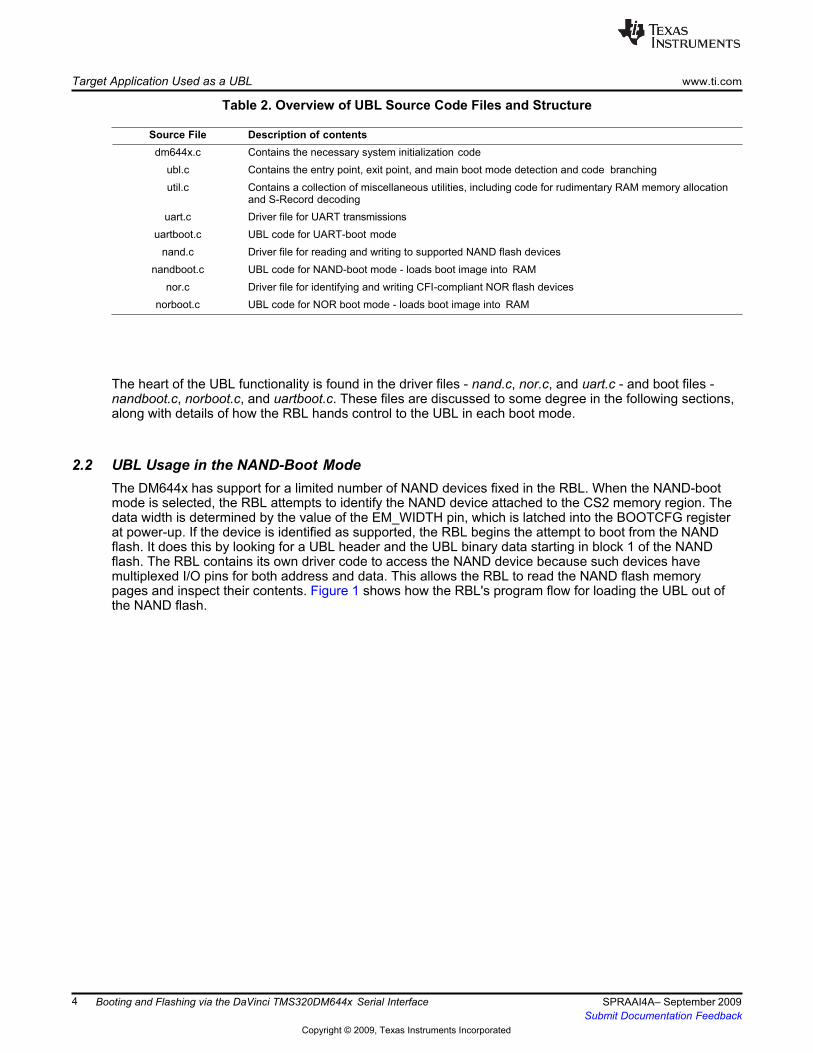
The DM644x has support for a limited number of NAND devices fixed in the RBL. When the NAND-boot mode is selected, the RBL attempts to identify the NAND device attached to the CS2 memory region. The data width is determined by the value of the EM_WIDTH pin, which is latched into the BOOTCFG register at power-up. If the device is identified as supported, the RBL begins the attempt to boot from the NAND flash. It does this by looking for a UBL header and the UBL binary data starting in block 1 of the NAND flash. The RBL contains its own driver code to access the NAND device because such devices have multiplexed I/O pins for both address and data. This allows the RBL to read the NAND flash memory pages and inspect their contents. Figure 1 shows how the RBL's program flow for loading the UBL out of the NAND flash.
4 Booting and Flashing via the DaVinci TMS320DM644x Serial Interface SPRAAI4A– September 2009 Submit Documentation Feedback
Copyright © 2009, Texas Instruments Incorporated
Target Application Used as a UBL www.ti.com
Fail
No First 32-Bit Word of Page is a Valid Magic
Number?
Yes
No All Pages Read Successfully?
Yes
Return and Jump to entryPoint
blockNum ++
0< (numPages * PageSize) <= 0x3800?
No
Yes
Fail Copy numPages Pages to IRAM
Assume a Valid Header. Treat the Four 32-Bit Words After the Magic Number as :
• entryPoint • numPages • startBlock • startPage
No
Figure 1. ROM Boot Loader NAND Mode Program Flow
As Figure 1 shows, the RBL attempts to find an acceptable magic number in the first four bytes of page 0 of the blocks 1 through 5 of the NAND memory. A list of valid magic numbers can be found in the TMS320DM644x DMSoC ARM Subsystem Reference Guide (SPRUE14). Different magic numbers enable certain features of the DM644x, such as cache and EDMA. Because the UBL code is small, in general it is safest to use UBL_MAGIC_SAFE without any noticeable performance penalty. If the other features are needed by the application or tertiary boot loader, they can be enabled as part of that code.
NOTE: If the NAND boot process fails, the RBL automatically tries to boot using the UART. The BOOTCFG bits still reflect that the DM644x boot pins are set for NAND-boot mode. It may be important to consider what chip peripherals are enabled by default in the different boot modes.
SPRAAI4A– September 2009 Booting and Flashing via the DaVinci TMS320DM644x Serial Interface 5 Submit Documentation Feedback
blockNum <=5
Yes
Read Page 0 of Block blockNum
Set blockNum = 1
Copyright © 2009, Texas Instruments Incorporated
Target Application Used as a UBL www.ti.com
NOTE: When the RBL reads the NAND memory pages, it always verifies the data by checking
ECC values. Appendix E provides details of how the RBL does this. Users who write UBLs to the NAND device need to acutely aware of how the ECC checks are handled or the NAND boot process will fail.
Once a valid magic number is found, the RBL assumes that a valid UBL header has been found in the first 20 bytes of the page (with the magic number occupying the first four of those 20 bytes). The structure of this header is shown in Table 3. The data in the header allows the RBL to locate the UBL image, copy it to the IRAM, and then begin executing it. The UBL begins by initializing all necessary subsystems of the DM644x and then checks what boot mode is in effect. A switch statement provides individual code paths for each boot mode. In the case of the NAND-boot mode, control passes to the NAND_copy() function in the file nandboot.c. The NAND_copy() function returns to the NAND device in the CS2 memory space and begins searching at page 0 of block 6 (because blocks 1 through 5 might contain the UBL) for the NAND application header. If the header is not found in block 6, the UBL tries each successive block up to block 50. The UBL, like the RBL, needs to have a NAND driver to access and read the NAND flash contents. The file nand.c contains all needed code to initialize, identify, read, write, and erase supported NAND memory devices. This application header, like the UBL header, contains the needed information to find and copy the application image from the NAND flash to the DDR RAM space. Its contents are detailed in Table 4. The magic number of this header indicates whether the image is in S-record form or binary form. The other entries are identical to those found in the UBL header. A new entry, the load address, tells the UBL where to load a binary image. An S-record image has this load address included as part of its format and ignores this field. Once the image is copied and, if needed, decoded, the UBL passes control to the code at the entry point address, concluding the boot loading process.
NOTE: If the NAND_Copy() function fails, the UBL defaults to trying to load an application image over the UART, as if a UART boot had been initiated. This behavior echoes that of the RBL when the NAND boot fails. The DVFlasher host application, described in more detail in Section 4, can be used to complete the operation using the noRBL command-line option.
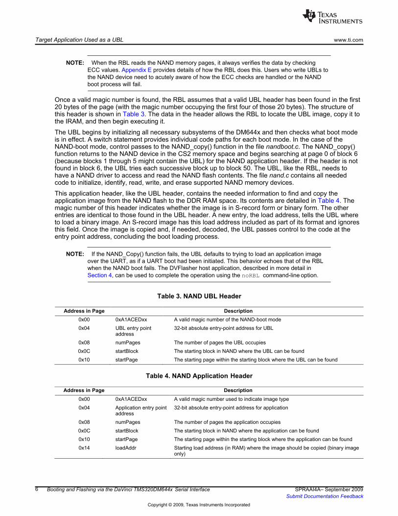
Table 3. NAND UBL Header
Address in Page Description
0x00 0xA1ACEDxx A valid magic number of the NAND-boot mode 0x04 UBL entry point
address 32-bit absolute entry-point address for UBL
0x08 numPages The number of pages the UBL occupies 0x0C startBlock The starting block in NAND where the UBL can be found 0x10 startPage The starting page within the starting block where the UBL can be found
Table 4. NAND Application Header
Address in Page Description
0x00 0xA1ACEDxx A valid magic number used to indicate image type 0x04 Application entry point
address 32-bit absolute entry-point address for application
0x08 numPages The number of pages the application occupies 0x0C startBlock The starting block in NAND where the application can be found 0x10 startPage The starting page within the starting block where the application can be found 0x14 loadAddr Starting load address (in RAM) where the image should be copied (binary image
only)
6 Booting and Flashing via the DaVinci TMS320DM644x Serial Interface SPRAAI4A– September 2009 Submit Documentation Feedback
Copyright © 2009, Texas Instruments Incorporated
Target Application Used as a UBL www.ti.com
2.3 UBL Usage in the NOR-Boot Mode
The main difference between using NAND flash and NOR flash memories via the AEMIF interface is that the NOR flash can be directly addressed as a memory device by the cpu, while a NAND device cannot. This means that the ARM core of the DM644x can execute code directly from a NOR flash in any of the CSx memory spaces. In NOR-boot mode, the RBL essentially detects the boot mode and then jumps to the CS2 memory region (address 0x02000000) to start executing the code found there. If the memory is empty, an exception will most likely occur, execution will return to the RBL, and the process will repeat in an infinite loop. There is no failsafe mechanism to execute a UART boot as there is with the NAND mode.
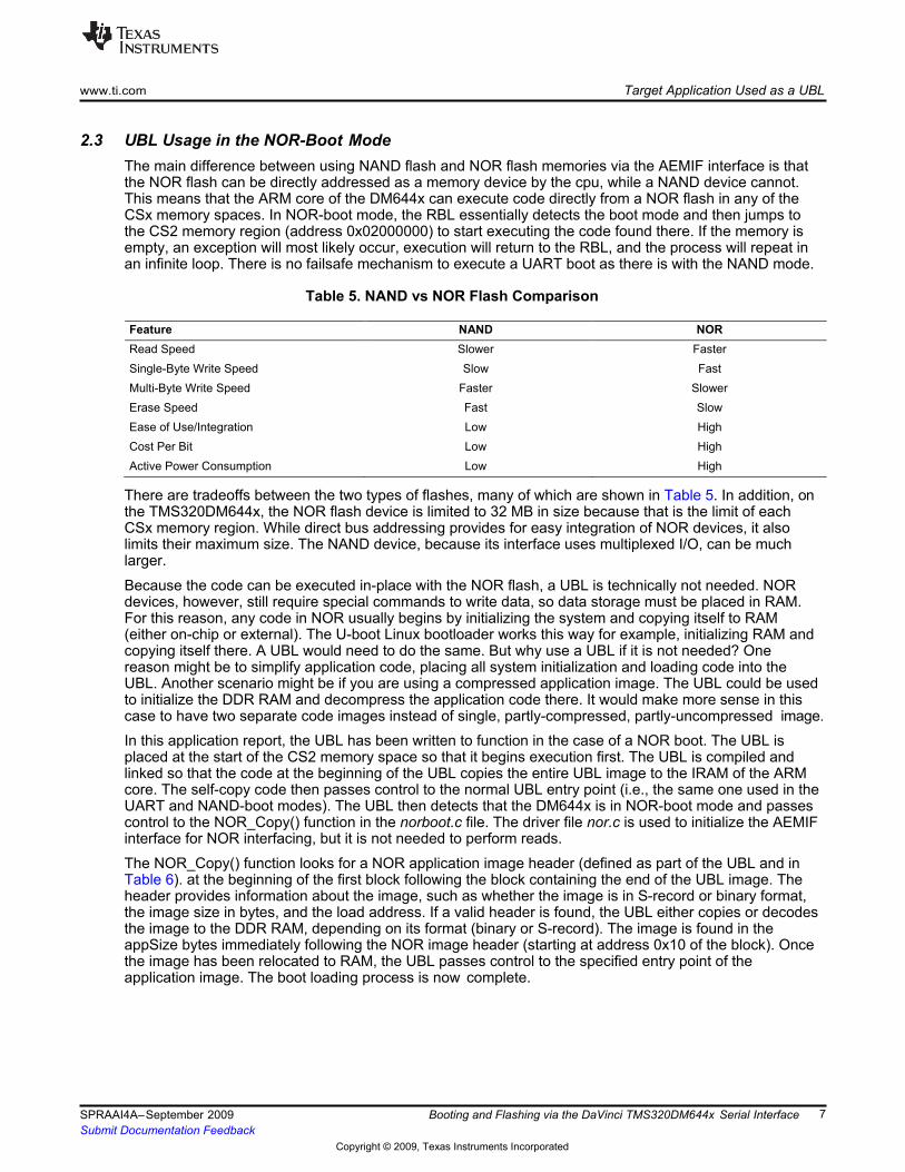
Table 5. NAND vs NOR Flash Comparison
Feature NAND NOR Read Speed Slower Faster Single-Byte Write Speed Slow Fast Multi-Byte Write Speed Faster Slower Erase Speed Fast Slow Ease of Use/Integration Low High Cost Per Bit Low High Active Power Consumption Low High
There are tradeoffs between the two types of flashes, many of which are shown in Table 5. In addition, on the TMS320DM644x, the NOR flash device is limited to 32 MB in size because that is the limit of each CSx memory region. While direct bus addressing provides for easy integration of NOR devices, it also limits their maximum size. The NAND device, because its interface uses multiplexed I/O, can be much larger. Because the code can be executed in-place with the NOR flash, a UBL is technically not needed. NOR devices, however, still require special commands to write data, so data storage must be placed in RAM. For this reason, any code in NOR usually begins by initializing the system and copying itself to RAM (either on-chip or external). The U-boot Linux bootloader works this way for example, initializing RAM and copying itself there. A UBL would need to do the same. But why use a UBL if it is not needed? One reason might be to simplify application code, placing all system initialization and loading code into the UBL. Another scenario might be if you are using a compressed application image. The UBL could be used to initialize the DDR RAM and decompress the application code there. It would make more sense in this case to have two separate code images instead of single, partly-compressed, partly-uncompressed image. In this application report, the UBL has been written to function in the case of a NOR boot. The UBL is placed at the start of the CS2 memory space so that it begins execution first. The UBL is compiled and linked so that the code at the beginning of the UBL copies the entire UBL image to the IRAM of the ARM core. The self-copy code then passes control to the normal UBL entry point (i.e., the same one used in the UART and NAND-boot modes). The UBL then detects that the DM644x is in NOR-boot mode and passes control to the NOR_Copy() function in the norboot.c file. The driver file nor.c is used to initialize the AEMIF interface for NOR interfacing, but it is not needed to perform reads. The NOR_Copy() function looks for a NOR application image header (defined as part of the UBL and in Table 6). at the beginning of the first block following the block containing the end of the UBL image. The header provides information about the image, such as whether the image is in S-record or binary format, the image size in bytes, and the load address. If a valid header is found, the UBL either copies or decodes the image to the DDR RAM, depending on its format (binary or S-record). The image is found in the appSize bytes immediately following the NOR image header (starting at address 0x10 of the block). Once the image has been relocated to RAM, the UBL passes control to the specified entry point of the application image. The boot loading process is now complete.
SPRAAI4A– September 2009 Booting and Flashing via the DaVinci TMS320DM644x Serial Interface 7 Submit Documentation Feedback
Copyright © 2009, Texas Instruments Incorporated
Target Application Used as a UBL www.ti.com
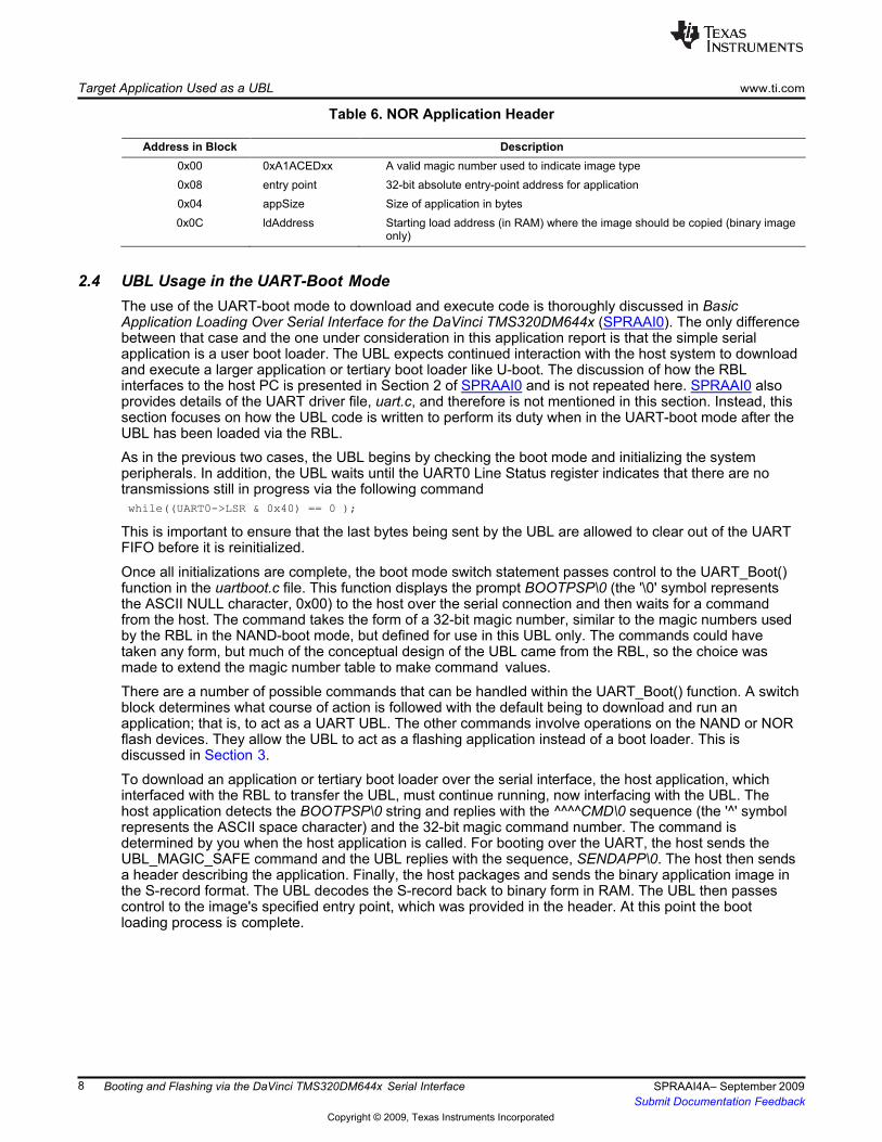
Table 6. NOR Application Header
Address in Block Description 0x00 0xA1ACEDxx A valid magic number used to indicate image type 0x08 entry point 32-bit absolute entry-point address for application 0x04 appSize Size of application in bytes 0x0C ldAddress Starting load address (in RAM) where the image should be copied (binary image
only)
2.4 UBL Usage in the UART-Boot Mode
The use of the UART-boot mode to download and execute code is thoroughly discussed in Basic Application Loading Over Serial Interface for the DaVinci TMS320DM644x (SPRAAI0). The only difference between that case and the one under consideration in this application report is that the simple serial application is a user boot loader. The UBL expects continued interaction with the host system to download and execute a larger application or tertiary boot loader like U-boot. The discussion of how the RBL interfaces to the host PC is presented in Section 2 of SPRAAI0 and is not repeated here. SPRAAI0 also provides details of the UART driver file, uart.c, and therefore is not mentioned in this section. Instead, this section focuses on how the UBL code is written to perform its duty when in the UART-boot mode after the UBL has been loaded via the RBL. As in the previous two cases, the UBL begins by checking the boot mode and initializing the system peripherals. In addition, the UBL waits until the UART0 Line Status register indicates that there are no transmissions still in progress via the following command while((UART0->LSR & 0x40) == 0 );
This is important to ensure that the last bytes being sent by the UBL are allowed to clear out of the UART FIFO before it is reinitialized. Once all initializations are complete, the boot mode switch statement passes control to the UART_Boot() function in the uartboot.c file. This function displays the prompt BOOTPSP\0 (the '\0' symbol represents the ASCII NULL character, 0x00) to the host over the serial connection and then waits for a command from the host. The command takes the form of a 32-bit magic number, similar to the magic numbers used by the RBL in the NAND-boot mode, but defined for use in this UBL only. The commands could have taken any form, but much of the conceptual design of the UBL came from the RBL, so the choice was made to extend the magic number table to make command values. There are a number of possible commands that can be handled within the UART_Boot() function. A switch block determines what course of action is followed with the default being to download and run an application; that is, to act as a UART UBL. The other commands involve operations on the NAND or NOR flash devices. They allow the UBL to act as a flashing application instead of a boot loader. This is discussed in Section 3. To download an application or tertiary boot loader over the serial interface, the host application, which interfaced with the RBL to transfer the UBL, must continue running, now interfacing with the UBL. The host application detects the BOOTPSP\0 string and replies with the ^^^^CMD\0 sequence (the '^' symbol represents the ASCII space character) and the 32-bit magic command number. The command is determined by you when the host application is called. For booting over the UART, the host sends the UBL_MAGIC_SAFE command and the UBL replies with the sequence, SENDAPP\0. The host then sends a header describing the application. Finally, the host packages and sends the binary application image in the S-record format. The UBL decodes the S-record back to binary form in RAM. The UBL then passes control to the image's specified entry point, which was provided in the header. At this point the boot loading process is complete.
8 Booting and Flashing via the DaVinci TMS320DM644x Serial Interface SPRAAI4A– September 2009 Submit Documentation Feedback

Copyright © 2009, Texas Instruments Incorporated
Target Application to Write to NAND or NOR Flash in UART-Boot Mode www.ti.com
3 Target Application to Write to NAND or NOR Flash in UART-Boot Mode Section 2.4 discusses how the UBL can be used to load an application image to the DDR RAM of the DM644x in the UART-boot mode. It is mentioned that there are other commands available in the UART_Boot() function to operate on the NAND or NOR Flash devices. This section describes in more detail these commands and how they work. Section 3.1 presents some preliminary details of how the UBL is compiled for use in flashing the NAND and NOR devices. Section 3.2 details how the NAND flashing code works, and Section 3.3 gives details of how the NOR flashing code works.
3.1 Notes Regarding Compilation of the UBL Binaries
The extra functionality that is available in the UART-boot mode increases code size. To support erasing and writing of all possible NOR flash configurations and all supported NAND devices adds significantly to the nand.c and nor.c driver files. The uartboot.c file also increases in size due to the added command paths. All the additional code results in the size of the UBL growing larger than the 14 kB limit that the RBL accepts. To overcome this issue, the code base must be divided into two separate UBLs. Because the desired operation is determined when the host application is called, the UBL can be split into a NAND version and a NOR version. The UBL downloaded at the start of the UART process will be correct based on the desired operation. If a UBL needs to be written to the flash memory, the correct version is again selected based on the operation selected on the command-line. If the selected operation is a simple boot loading operation, either version can be used. To accomplish this UBL partitioning, the C code uses preprocessor directives to enable conditional compilation. The Makefile is written such that the UBL code is compiled twice with two different #defines passed via the gcc command-line. The result is two binary files, ubl_davinci_nor.bin and ubl_davinci_nand.bin. The code affected by the conditional #defines includes the following: • NAND and NOR cases of boot mode switch statement in the main() function of ubl.c • nand.c and nandboot.c (only compiled for NAND UBL) • nor.c and norboot.c (only compiled for NOR UBL) • NAND and NOR command cases of the command switch statement in the uartboot() function in
uartboot.c
These two distinct binary files are then embedded in the host executable as resources. When the host is called with a command that targets the NOR memory, the NOR UBL is accessed and transmitted to the target. When the host is called with a command that targets the NAND memory, the NAND UBL is accessed and transmitted to the target instead.
3.2 NAND Flash Support
In the NAND UBL there are three commands available to operate on the NAND flash. These are defined in Table 7. The first two commands are used to write a NAND UBL and application image to the NAND flash attached to the CS2 AEMIF, in either S-record or binary form. (The S-record image is approximately three times larger than the binary image.) The last command is used to perform a global erase of the NAND device. There is no command to perform a local erase over a smaller range, though the write command does erase individual blocks that it puts data into. These commands are discussed in the following sections. The discussion of code is not extend to the low-level details of how to interface with (i.e., read, write, erase) supported NAND flash devices. Only the highest, most abstract functions of the nand.c driver file are discussed. For reference, a list of supported NAND flash devices is supplied in Appendix D.
Table 7. Table of Acceptable NAND Commands for Use in NAND UBL UART-Boot Mode
Command Name Command Value
UBL_MAGIC_NAND_SREC_BURN 0xA1ACEDBB UBL_MAGIC_NAND_BIN_BURN 0xA1ACEDCC UBL_MAGIC_NAND_GLOBAL_ERASE 0xA1ACEDDD
SPRAAI4A– September 2009 Booting and Flashing via the DaVinci TMS320DM644x Serial Interface 9 Submit Documentation Feedback

Copyright © 2009, Texas Instruments Incorporated
Target Application to Write to NAND or NOR Flash in UART-Boot Mode www.ti.com
3.2.1 NAND Flashing Commands
The two NAND flashing commands are used to write four items to the NAND flash. These items are the NAND UBL header, the NAND UBL binary, an application image header, and the application image. The only difference between these two commands is the type of the application image. It can be either an S-record or a binary image. As seen in Table 4, the application image header contains a magic number, which indicates the format of the image. The possible values of this number and their meanings are shown in Table 8. Since the two commands are so similar, they jointly use a single case of the uartboot.c's command switch statement. The code for this is given in Section A.1.0.
Table 8. NAND Application Image Header Magic Number
Number Name Number Value Description UBL_MAGIC_SAFE 0xA1ACED00 Indicates that the application image is in S-record format. UBL_MAGIC_BIN_IMG 0xA1ACED66 Indicates that the application image is in binary format.
When the NAND flash command code begins executing, it issues the SENDUBL\0 prompt to indicate that the DM644x is waiting for the flash-bound UBL to be transmitted. The UBL code calls the UARTGetHeaderAndData(&ackHeader) function, found in the uart.c driver file, to receive the acknowledgement header and the image data from the host. All images transferred over the serial link are in S-record format. When they are received, they are decoded to a binary format to verify the data integrity. When the UARTGetHeaderAndData(&ackHeader) call returns, there are two versions of the image in DDR memory - one binary and one S-record. The ackHeader struct holds the address to both versions, as well as information about the size of both versions, the binary entry point, and the magic number. When the received image is a UBL UBL, only the binary data is used. After the UBL is received, the NAND is initialized by a call to NAND_Init(), found in the nand.c driver file. The NAND UBL header is assigned appropriate values, some of which were received by UARTGetHeaderAndData(). The header and the data are written to the NAND memory through a call to NAND_WriteHeaderAndData(), also defined in the NAND driver file, with block 1 as the destination. Based on a given block destination, this function determines if this data is a UBL or application and attempts the appropriate number of rewrites if there are blocks with errors. (See Section 2.2 for details on how bad blocks are handled in the boot process.) The process outlined above begins again when the UBL requests the application image by sending the sequence SENDAPP\0. The host again transmits a header and data, and the target receives them via the UARTGetHeaderAndData() function. The NAND application header is set up and the header and data are written to the NAND flash by calling NAND_WriteHeaderAndData(). The difference in this case, is that the address of the image and the number of bytes in the image are selected between the S-record and binary versions depending on the value of the magic number. If, at any time during these operations, a failure occurs, the program flow terminates and the UART boot starts again by sending the BOOTPSP\0 sequence and waiting for the ^^^^CMD\0 sequence and a command value from the host.
3.2.2 NAND Erase Command
The NAND erase command does not require any further input from the host via the serial port. NAND devices are erased on a block basis. This code erases blocks 1 through the last block of the device. Block 0 is never touched, whether the operation is writing or erasing. First the NAND device is initialized by calling NAND_Init(). This function call populates the gNandInfo structure with the values defining the NAND interface and the identified device. Then the blocks that are to be erased are first unprotected by calling NAND_UnProtectBlocks() with the range of block numbers. NAND_EraseBlocks() is then called on that same range of blocks (which should be all blocks but block 0). If the erasure completes without error, the NAND_ProtectBlocks() function is called to protect all blocks in the device. Details of the code can be found in Section A.2.0. The NAND erase function does require a measurable amount of time, but it is significantly quicker than the erasure of a similarly-sized NOR device.
10 Booting and Flashing via the DaVinci TMS320DM644x Serial Interface SPRAAI4A– September 2009 Submit Documentation Feedback

Copyright © 2009, Texas Instruments Incorporated
Target Application to Write to NAND or NOR Flash in UART-Boot Mode www.ti.com
3.3 NOR Flash Support In the NOR UBL there are four commands available to operate on the NOR flash. These are defined in Table 9. The first command does not have an analog in the set NAND flash commands. The remaining three commands mirror the three NAND commands. All of these commands are discussed in the following sections. As in the NAND case, the discussion does not consider many details of the NOR driver file, nor.c. A few details of the hardware cases that the NOR driver file supports can be found in Appendix C.
Table 9. Table of Acceptable NOR Commands for Use in NOR UBL UART-Boot Mode
Command Name Command Value
UBL_MAGIC_NOR_RESTORE 0xA1ACED77 UBL_MAGIC_NOR_SREC_BURN 0xA1ACED88 UBL_MAGIC_NOR_BIN_BURN 0xA1ACED99 UBL_MAGIC_NOR_GLOBAL_ERASE 0xA1ACEDAA
3.3.1 NOR Restore Command
The UBL_MAGIC_NOR_RESTORE command is used to place a downloaded image at the start of the NOR flash without a UBL. The image should be executable starting at its base and perform any needed system initialization routines because the UBL is not in place to do this. This command is called the RESTORE command since its primary purpose is to return the Spectrum Digital DVEVM to a bootable state by writing a NOR U-boot image to the NOR flash (without having to use CCS),though tchnically any data can be written to the start of the NOR flash with this command. The NOR U-boot image contains all needed initialization and start-up code and can be further used to boot and use Linux® software to restore the hard drive contents, etc. The code to execute this command, found in uartboot.c, is included in Section A.3.0. The code shows that the UBL responds to the restore commands with the SENDAPP\0 sequence. The host application then sends the header and application image, which the UBL reads with the same UARTGetHeaderAndData() function. NOR_Init() is called to identify and initialize the flash memory. This step fills the gNorInfo structure with important information about the flash device(s), including its total size, the number and size of its blocks, and the command set used to access the device(s). The blocks that will contain the binary bytes of the UBL, starting at the base of the flash memory (0x02000000), are then erased by calling NOR_Erase(). Finally, the data is written to the NOR flash using the NOR_WriteBytes() command.
3.3.2 NOR Flash Commands
The UBL_MAGIC_NOR_SREC_BURN and UBL_MAGIC_NOR_BIN_BURN commands mirror the NAND versions in function. The main difference is the manner in which the UBL is handled. In the NAND version, the UBL must be written with a header to certain location in the NAND device. In this way the RBL can find the header and know how to find and read the UBL. In the case of the NOR flash, the RBL does not do anything except pass execution to the start of NOR flash. The NOR UBL is written to the base of the flash so it begins execution in the NOR-boot mode. Moreover, the UBL image is laid out such that a block of self-copy code is found at the beginning of the UBL image. This code can be seen in Appendix B. After the UBL copies itself to the ARM internal RAM, the UBL entry point, the boot() function, is called and the UBL begins its normal execution.
SPRAAI4A– September 2009 Booting and Flashing via the DaVinci TMS320DM644x Serial Interface 11 Submit Documentation Feedback
Copyright © 2009, Texas Instruments Incorporated
Host Application www.ti.com
The code in Section A.4.0 shows how the NOR flash setup uses the UBL in this way. Upon receipt of the NOR flash command, the UBL responds with the SENDUBL/0 sequence and then receives the UBL data via the UARTGetHeaderAndData() function. The flash blocks that will hold this binary data (block 0 and any needed sequential blocks) are erased. The binary bytes are written to the memory (writing can take place on individual bytes, not just entire blocks). The UBL then requests the application image via the SENDAPP/0 sequence. The data is again received via the UARTGetHeaderAndData() command. The magic number of the header is examined to determine if the S-record image or decoded binary image should be written to the NOR flash (see Table 8). The number of blocks needed for the image header and data is then calculated and the blocks are erased, starting at the first block after the last block occupied by the UBL. This avoids erasure of any UBL code and provides a common starting location for the NOR_Copy() function (found in norboot.c) to look for the application image. The header and the application image are written to consecutive memory locations with no gaps between them.
3.3.3 NOR Erase Command
The NOR global erase command is simple. Once the command is received, NOR_Init() is called to setup the NOR and learn its parameters. Then the UBL executes the erase command by calling NOR_GlobalErase(), which in turn calls the more general NOR_Erase() function using the flash base address and the flash size as parameters. These parameters were set up in the NOR_Init() function. The erase of the NOR flash is slow, taking several minutes for the largest supported devices.
4 Host Application
The host application is a critical part of the functioning that is exposed in the example UBL's UART-boot mode. It is important to realize that the UBL and the host application must be jointly developed to take advantage of the extra capability provided by an independent host. Each program must be written with the other in mind so that they can interface properly to achieve desired results. To emphasize this point, it should be noted that the binary NAND and NOR UBLs generated by the ARM cross-compiler tools are embedded into the host application binary (that is they become part of the host executable) so that they can always be used as the basis for interfacing during the UART-boot mode. Another UBL would not suffice to allow the execution of the commands described in Section 3. This section provides some details of the DVFlasher host application. The source code is available with this application note. The readme.txt file in the source archive has more details about the application, including how to compile it.
4.1 General Information
The host application was written in the C# language. C# is a standardized object-oriented programming language (ECMA and ISO standards) that, like Java, aims to be cross platform by targeting a common language infrastructure (CLI). An implementation of the CLI has been developed for multiple platforms and programs compiled on one platform for one implementation should work equally well on another. This is accomplished partially because the compiled code exists as an intermediate language. Surrounding the CLI, there can be a precompiled framework of classes that are used to perform common functions and provide basic utilities (much like the standard libraries of C or C++). Microsoft ® Corporation has provided a framework of this type known as the Microsoft ® .Net Framework, currently at version 3.0. An open source project sponsored by Novell ®,called the Mono Project, has developed an open-source cross-platform CLI and framework that is mostly compatible (and aims to be fully compatible) with Microsoft's closed .Net Framework. The provided host application has been tested and verified to work on both frameworks. As a result, the application can be used on a host running Microsoft Windows ® or any recent Linux distribution. Under Windows, the application can use either the .Net Framework (provided for free at http://www.microsoft.com/) or the Mono Framework (available at http://www.mono-project.com/). Under Linux, the Mono Framework is the only option. The code is found in the DVFlasher.cs and CRC32.cs files. The compiled executable is DVFlasher_X_YY.exe,where X is the major revision number and YY is the minor revision number. Each source file provides a single class - a main program class and a CRC32 class. The CRC32 is used in the RBL negotiations. The main class holds all the remaining functionality of the application. Its most important job is to spawn the worker thread, which handles all serial port communications with the DM644x, and monitor key presses that indicate a user abort.
12 Booting and Flashing via the DaVinci TMS320DM644x Serial Interface SPRAAI4A– September 2009 Submit Documentation Feedback
Copyright © 2009, Texas Instruments Incorporated
Host Application www.ti.com
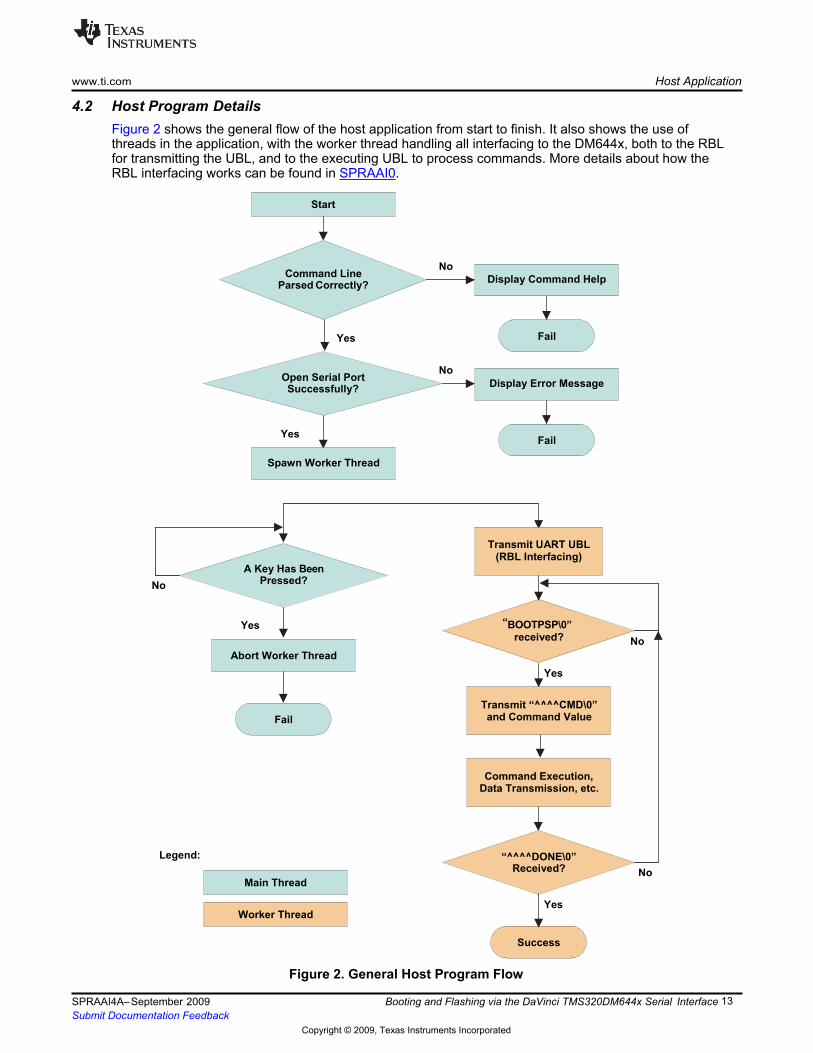
4.2 Host Program Details Figure 2 shows the general flow of the host application from start to finish. It also shows the use of threads in the application, with the worker thread handling all interfacing to the DM644x, both to the RBL for transmitting the UBL, and to the executing UBL to process commands. More details about how the RBL interfacing works can be found in SPRAAI0.
Figure 2. General Host Program Flow
SPRAAI4A– September 2009 Booting and Flashing via the DaVinci TMS320DM644x Serial Interface 13 Submit Documentation Feedback
Command Line Parsed Correctly?
No
Yes
Open Serial Port Successfully?
No
Yes
Spawn Worker Thread
Start
No A Key Has Been
Pressed?
Yes “BOOTPSP\0” received? No
Yes
Legend: “^^^^DONE\0” Received? No
Yes
Success
Command Execution,
Data Transmission, etc.
Transmit “^^^^CMD\0” and Command Value
Transmit UART UBL
(RBL Interfacing)
Worker Thread
Main Thread
Fail
Display Command Help
Fail
Display Error Message
Fail
Abort Worker Thread
Copyright © 2009, Texas Instruments Incorporated
Host Application www.ti.com
The UBL interfacing depends on a series of sequences that are agreed upon by the UBL and host. Like other design features (such as the magic numbers), these sequences resemble the sequences used in the RBL for negotiation with the host (eight bytes, including null terminator). Table 10 shows these sequences and describes how they are used. Note that the '^' symbol is used to indicate the ASCII space character
Table 10. UBL/Host Interfacing Sequences
Sequence Produced By Description
BOOTPSP\0 UBL Initiating sequence indicating UBL has been loaded correctly and is awaiting a command
^^^^CMD\0 Host Prefix sent before the command intended for execution by the UBL SENDUBL\0 UBL Sequence to instruct the host to send the UBL that will be written into the flash
memory (NOR or NAND) SENDAPP\0 UBL Sequence to instruct the host to send the application image that will be written into
the flash memory or run from RAM ^^^^ACK\0 Host Sequence sent as prefix to the header attached to all S-record images, which is
parsed by the UARTGetHeaderAndData() function on the UBL ^^BEGIN\0 UBL Sequence sent by the UARTGetHeaderAndData() function to indicate that ACK
header was received and the UBL is now ready to receive the S-record data ^^^DONE\0 UBL Sequence to indicate successful reception of all S-record bytes, successful
completion of S-record decode, and successful completion of the entire UBL command
The DVFlasher class consists of a number of functions (or methods) that are used in one of the two threads seen in Figure 2. The following sections outline what these functions are and what they do. No details of the code itself will be given, though the reader is encouraged to refer to the source files to understand how the functions work. This is especially true if the reader intends to use this source as a starting point for their own application.
4.2.1 Main Thread Functions
• private static void DispHelp() This function displays a screen of help on how to use the program.
• public static ProgramCmdParams ParseCmdLine(String[] args) This function parses the input command line arguments and poulates a struct of the pertinent information. It also sets up and
• static Int32 Main(String[] args) This function is the entry point for the entire application. It calls ParseCmdLine() and then sets up and opens the serial port. Finally it spawns the worker thread to handle the RBL and UBL serial negotiations. While the worker thread executes, the main function monitors key presses that would signify a user abort.
4.2.2 Worker Thread Functions
• public static void WorkerThreadStart() This function is the entry point and main function for the worker thread.
• private static Stream GetEmbeddedUBLStream() This function is used to access the NAND or NOR UBLs embedded in the host executable. The NOR UBL is accessed by default unless a NAND command is being called.
• private static Byte[] GetFileData(String filename, UInt32 decAddr) This function is used to access data from the binary application files that are to be sent via the UART.
• private static void TransmitUARTUBL() This function is called first by the WorkerThreadStart()function to transmit the UART UBL via negotiations with the ARM ROM bootloader.
• private static Boolean TransmitCMDSuccessful() This function is called to send the user-selected command to the UART UBL executing on the DM644x. It waits for the BOOTPSP\0 sequence and responds with the ^^^^CMD\0 sequence and the command number. It then waits for a ^^^DONE\0 sequence.
14 Booting and Flashing via the DaVinci TMS320DM644x Serial Interface SPRAAI4A– September 2009
Submit Documentation Feedback
Copyright © 2009, Texas Instruments Incorporated
References www.ti.com
• private static void TransmitErase() This function sends the erase command (NAND or NOR) and then awaits a ^^^DONE\0 sequence indicating successful completion.
• private static void TransmitAPP() This fucntion is used to transmit an application image only. It is called when the -r or -b command-line options are selected.
• private static void TransmitFLASHUBLandAPP() This function is used with the NAND and NOR flashing commands where a UBL and an application image will be written to the flash device.
• private static Boolean waitForSequence(String str,String altStr,SerialPort sp,Boolean verbose) This function is used to wait for a particular sequence on the serial port (the string str). It also will detect an alternate sequence that would indicate failure (the string altStr). The boolean verboseallows the output from the DM644x to be shown or suppressed.
• private static Boolean waitForSequence(String str,String altStr,SerialPort sp) This function is the same as the previous except now the verbosity is chosen by the command-line option -v.
5 References
• Basic Application Loading over the Serial Interface for the DaVinci TMS320DM644x (SPRAAI0) • TMS320DM644x DMSoC ARM Subsystem Reference Guide (SPRUE14) • TMS320DM644x DMSoC DDR2 Memory Controller User's Guide (SPRUE22) • TMS320DM644x DMSoC Universal Asynchronous Receiver/Transmitter (UART) User's Guide
(SPRUE33) • NAND vs. NOR Flash Memory, Toshiba America Electronics Components, Inc., 2006,
http://www.toshiba.com/taec/components/Generic/Memory_Resources/NANDvsNOR.pdf. • Common Flash Interface (CFI) and Command Sets,AN 646, Intel, Inc., April 2000,
http://download.intel.com/design/flcomp/applnots/29220404.pdf
SPRAAI4A– September 2009 Booting and Flashing via the DaVinci TMS320DM644x Serial Interface 15 Submit Documentation Feedback

Copyright © 2009, Texas Instruments Incorporated
Appendix A www.ti.com
Appendix A UART-Boot Mode Flash Command Code
This appendix shows the UBL code from the uartboot.c file that implements the NAND and NOR flashing functionality that is available in the device's UART-boot mode.
A.1 NAND Flashing Code
If ( UARTSendData((Uint8*)"SENDUBL", TRUE) != E_PASS) goto UART_tryAgain; // Get the UBL into binary form if (UARTGetHeaderAndData(&ackHeader) != E_PASS) { goto UART_tryAgain; } // Initialize the NAND Flash NAND_Init(); // Get magicNum nandBoot.magicNum = ackHeader.magicNum; // Get entrypoint for UBL nandBoot.entryPoint = (Uint32) (0x0000FFFF & ackHeader.appStartAddr); // The UBL image is 14kBytes plus do some rounding nandBoot.numPage = 0; while ( (nandBoot.numPage * gNandInfo.bytesPerPage) < (0x3800)) { nandBoot.numPage++; } // The page is always page 0 for the UBL header, so we use page 1 for data nandBoot.page = 1; // The block is always block is always 1 (to start with) for the UBL header nandBoot.block = START_UBL_BLOCK_NUM; // This field doesn't matter for the UBL header nandBoot.ldAddress = 0; // Write header to page 0 of block 1(or up to block 5) // Write the UBL to the same block, starting at page 1 (since blocks are 16k) UARTSendData((Uint8 *) "Writing UBL to NAND flash\r\n", FALSE); if (NAND_WriteHeaderAndData(&nandBoot, (Uint8 *) ackHeader.binAddr) != E_PASS) goto UART_tryAgain; // Send SENDAPP command if (UARTSendData((Uint8*)"SENDAPP", TRUE) != E_PASS) goto UART_tryAgain; // Get the application header and data if (UARTGetHeaderAndData(&ackHeader) != E_PASS) { goto UART_tryAgain; } // Set parameters depending on whether binary or srecord if (bootCmd == UBL_MAGIC_NAND_SREC_BURN) { dataByteCnt = ackHeader.srecByteCnt; dataAddr = ackHeader.srecAddr; } else if (bootCmd == UBL_MAGIC_NAND_BIN_BURN) { dataByteCnt = ackHeader.binByteCnt; dataAddr = ackHeader.binAddr; } // Rely on the host applciation to send over the right magic number (safe or bin) nandBoot.magicNum = ackHeader.magicNum; // Use the entrypoint received in ACK header nandBoot.entryPoint = ackHeader.appStartAddr; // The APP s-record image is dataByteCnt bytes plus do some rounding nandBoot.numPage = 0; while ( (nandBoot.numPage * gNandInfo.bytesPerPage) < dataByteCnt ) { nandBoot.numPage++; } // The page is always page 0 for the header, so we use page 1 for data nandBoot.page = 1; // The block is always 6 (to start with) for the APP header nandBoot.block = START_APP_BLOCK_NUM; // The load address is only important if this is a binary image nandBoot.ldAddress = ackHeader.binAddr; // Nand Burn of application data UARTSendData((Uint8 *) "Writing APP to NAND flash\r\n", FALSE); if (NAND_WriteHeaderAndData(&nandBoot, (Uint8 *) dataAddr) != E_PASS) goto UART_tryAgain; // Set the entry point to nowhere, since there isn't an appropriate binary image to run */ gEntryPoint = 0x0; break;
A.2 NAND Erasing Code if (NAND_Init() != E_PASS) goto UART_tryAgain; // Unprotect the NAND Flash NAND_UnProtectBlocks(1,gNandInfo.numBlocks - 1); // Erase all the pages of the device if (NAND_EraseBlocks(1,(gNandInfo.numBlocks - 1)) != E_PASS) { UARTSendData((Uint8 *)"Erase failed.\r\n", FALSE); goto UART_tryAgain; } else { UARTSendData((Uint8 *)"Erase completed successfully.\r\n", FALSE); } // Protect the device NAND_ProtectBlocks(); // Set the entry point for code execution // Go to reset in this case since no code was downloaded gEntryPoint = 0x0; break;
16 SPRAAI4A– September 2009 Submit Documentation Feedback

Copyright © 2009, Texas Instruments Incorporated
NOR Restore Code www.ti.com
A.3 NOR Restore Code // Get the APP (should be u-boot) into binary form if ( UARTSendData((Uint8*)"SENDAPP", TRUE) != E_PASS) goto UART_tryAgain; if ( UARTGetHeaderAndData(&ackHeader) != E_PASS ) goto UART_tryAgain; // Initialize the NOR Flash if ( NOR_Init() != E_PASS ) goto UART_tryAgain; // Erasing the Flash if ( NOR_Erase(gNorInfo.flashBase, ackHeader.binByteCnt) != E_PASS ) goto UART_tryAgain; // Write the actual application to the flash if ( NOR_WriteBytes(gNorInfo.flashBase, ackHeader.binByteCnt, ackHeader.binAddr) != E_PASS ) goto UART_tryAgain; // Set the entry point for code execution gEntryPoint = gNorInfo.flashBase; break;
A.4 NOR Flashing Code if ( UARTSendData((Uint8*)"SENDUBL", TRUE) != E_PASS) goto UART_tryAgain; // Get the UBL into binary form if (UARTGetHeaderAndData(&ackHeader) != E_PASS) { goto UART_tryAgain; } // Initialize the NOR Flash NOR_Init(); // Erasing the Flash NOR_Erase(gNorInfo.flashBase, ackHeader.binByteCnt); // Write binary UBL to NOR flash NOR_WriteBytes(gNorInfo.flashBase, ackHeader.binByteCnt, ackHeader.binAddr); // Send SENDAPP command if ( UARTSendData((Uint8*)"SENDAPP", TRUE) != E_PASS) goto UART_tryAgain; // Get the application header and data if (UARTGetHeaderAndData(&ackHeader) != E_PASS) { goto UART_tryAgain; } // Determine whether to use binary or srec if (bootCmd == UBL_MAGIC_NOR_BIN_BURN) { dataByteCnt = ackHeader.binByteCnt; dataAddr = ackHeader.binAddr; } else if (bootCmd == UBL_MAGIC_NOR_SREC_BURN) { dataByteCnt = ackHeader.srecByteCnt; dataAddr = ackHeader.srecAddr; } // Erase the NOR flash where header and data will go DiscoverBlockInfo( (gNorInfo.flashBase + UBL_IMAGE_SIZE), &blkSize, &blkAddress ); baseAddress = (blkAddress + blkSize); NOR_Erase( baseAddress, (dataByteCnt + sizeof(norBoot)) ); norBoot.magicNum = ackHeader.magicNum; //MagicFlag for Application (binary or safe) norBoot.appSize = dataByteCnt; //Bytes of application (either srec or binary) norBoot.entryPoint = ackHeader.appStartAddr; //Value from ACK header norBoot.ldAddress = ackHeader.binAddr; //Should be same as AppStartAddr // Write the NOR_BOOT header to the flash NOR_WriteBytes( baseAddress, sizeof(norBoot), (Uint32) &norBoot); // Write the application data to the flash NOR_WriteBytes((baseAddress + sizeof(norBoot)), dataByteCnt, dataAddr); // Set the entry point for code execution to the newly copied binary UBL gEntryPoint = gNorInfo.flashBase; break;
A.5 NOR Erasing Code NOR_Init(); // Erasing the Flash if (NOR_GlobalErase() != E_PASS) { UARTSendData((Uint8 *)"\r\nErase failed.\r\n", FALSE); } else { UARTSendData((Uint8 *)"\r\nErase completed successfully.\r\n", FALSE); } // Set the entry point for code execution // Go to reset in this case since no code was downloaded gEntryPoint = 0x0; break;
SPRAAI4A– September 2009 Booting and Flashing via the DaVinci TMS320DM644x Serial Interface 17 Submit Documentation Feedback
Copyright © 2009, Texas Instruments Incorporated
Appendix B www.ti.com
Appendix B Self-Copy Code for NOR UBL
The self-copy function is prototyped in the ubl.h file as void selfcopy( void ) attribute ((naked,section (".selfcopy")));
The linker script sets the.selfcopy run-time address at the beginning of the CS2 memory space, where the NOR flash should be. Its load address, which determines its place in the binary file, is set for 0x0. Therefore, when the binary imaged is placed in the NOR flash, the self-copy code is located at 0x02000000, which is its correct run-time address. The self-copy function is defined in the ubl.c file as void selfcopy() { // Self copy setup extern Uint32 selfcopysrc, selfcopydest, selfcopydestend; //Enable ITCM asm(" MRC p15, 0, r0, c9, c1, 1"); asm(" MOV r0, #0x1"); asm(" MCR p15, 0, r0, c9, c1, 1"); //Enable DTCM asm(" MRC p15, 0, r0, c9, c1, 0"); asm(" MOV r0, #0x8000"); asm(" ORR r0, r0, #0x1"); asm(" MCR p15, 0, r0, c9, c1, 0"); VUint32* src = &( selfcopysrc); VUint32* dest = &( selfcopydest); VUint32* destend = &( selfcopydestend); // Copy the words while (dest < destend) { *dest = *src; dest++; src++; } //Jump to the normal entry point boot(); }
The selfcopy() function uses symbols from the linker command script, ubl_davinci.lds ( selfcopysrc, selfcopydest, selfcopydestend) to copy the data from the NOR flash in the CS2 memory space to the IRAM. The assembly instructions ensure that the IRAM blocks are enabled. Finally the function calls the boot() function, which is the normal UBL entry located in IRAM.
18 SPRAAI4A– September 2009 Submit Documentation Feedback
Copyright © 2009, Texas Instruments Incorporated
Appendix C www.ti.com
Appendix C Supported NOR Devices and Configurations C.1 NOR AEMIF Information
The AEMIF interface of the TMS320DM644x can operate in 16-bit or 8-bit widths. The maximum addressable size in 16-bit mode is 32MB, while in 8-bit mode it is only 16 MB. Code can be placed in a NOR flash device and executed directly in the NOR-boot mode. The EM_WIDTH pin must be set to match the width of the device or acess to the NOR device will fail.
C.2 Supported NOR Configurations
The nor.c driver code should detect and support the configuration listed in Table 11. For the driver to properly detect the number of devices and their configuration, all devices must be compliant with the Common Flash Interface (CFI) specification. Any recent NOR flash device should be CFI-compliant, but you should verify this with the devices' datasheet. Byt querying the CFI information on the device, the driver can appropriately decide to use the AMD command set or the Intel command set.
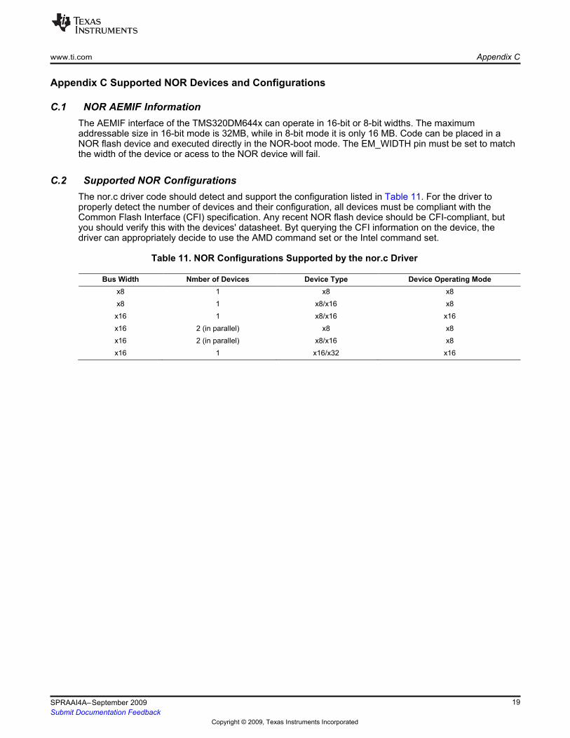
Table 11. NOR Configurations Supported by the nor.c Driver
Bus Width Nmber of Devices Device Type Device Operating Mode
x8 1 x8 x8 x8 1 x8/x16 x8 x16 1 x8/x16 x16 x16 2 (in parallel) x8 x8 x16 2 (in parallel) x8/x16 x8 x16 1 x16/x32 x16
SPRAAI4A– September 2009 19 Submit Documentation Feedback

Copyright © 2009, Texas Instruments Incorporated
Appendix D www.ti.com
Appendix D Supported NAND Devices
Table 12 shows the device IDs and the parameters of the supported NAND devices. These devices are the bootable devices that the TMS320DM644x supports. Additional non-bootable (i.e not supported by the ROM) devices could easily be handled by the nand.c driver by expanding the device table, which is found at the top of the NAND driver file, nand.c.
Table 12. NAND Devices Supported by the nand.c Driver
Device ID Number of Blocks Pages Per Block Bytes Per Page Total Size
0x6E 256 16 256+8 1 MB 0x68 256 16 256+8 1 MB 0xEC 256 16 256+8 1 MB 0xE8 256 16 256+8 1 MB 0xEA 512 16 256+8 2 MB 0xE3 512 16 512+16 4 MB 0xE5 512 16 512+16 4 MB 0xE6 1024 16 512+16 8 MB 0x39 1024 16 512+16 8 MB 0x6B 1024 16 512+16 8 MB 0x73 1024 32 512+16 16 MB 0x33 1024 32 512+16 16 MB 0x75 2048 32 512+16 32 MB 0x35 2048 32 512+16 32 MB 0x43 1024 32 512+16 16 MB 0x45 2048 32 512+16 32 MB 0x53 1024 32 512+16 16 MB 0x55 2048 32 512+16 32 MB 0x36 4096 32 512+16 64 MB 0x46 4096 32 512+16 64 MB 0x56 4096 32 512+16 64 MB 0x76 4096 32 512+16 64 MB 0x74 8192 32 512+16 128 MB 0x79 8192 32 512+16 128 MB 0x71 16384 32 512+16 256 MB 0xF1 1024 64 2048+64 128 MB 0xA1 1024 64 2048+64 128 MB 0xAA 2048 64 2048+64 256 MB 0xDA 2048 64 2048+64 256 MB 0xDC 4096 64 2048+64 512 MB 0xAC 4096 64 2048+64 512 MB 0xB1 1024 64 2048+64 128 MB 0xC1 1024 64 2048+64 128 MB
20 SPRAAI4A– September 2009 Submit Documentation Feedback
Copyright © 2009, Texas Instruments Incorporated
Appendix E www.ti.com
Appendix E NAND ECC Considerations
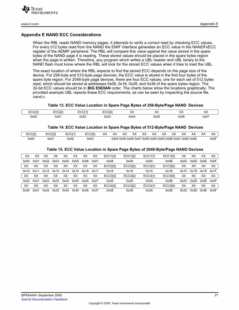
When the RBL reads NAND memory pages, it attempts to verify a correct read by checking ECC values. For every 512 bytes read from the NAND the EMIF interface generates an ECC value in the NANDFxECC register of the AEMIF peripheral. The RBL will compare this value against the value stored in the spare bytes of the NAND page it is reading. These stored values should be placed in the spare bytes region when the page is written. Therefore, any program which writes a UBL header and UBL binary to the NAND flash must know where the RBL will look for the stored ECC values when it tries to load the UBL. The exact location of where the RBL expects to find the stored ECC depends on the page size of the device. For 256-byte and 512-byte page devices, the ECC value is stored in the first four bytes of the spare byte region. For 2048-byte page devices, there are four ECC values, one for each set of 512 bytes read, which should be stored at addresses 0x08, 0x18, 0x28, and 0x38 of the spare bytes region. The 32-bit ECC values should be in BIG ENDIAN order. The charts below show the locations graphically. The provided example UBL repects these ECC requirements, as can be seen by inspecting the source file, nand.c.
Table 13. ECC Value Location in Spare Page Bytes of 256-Byte/Page NAND Devices
ECC[3] ECC[2] ECC[1] ECC[0] XX XX XX XX 0x00 0x01 0x02 0x03 0x04 0x05 0x06 0x07
Table 14. ECC Value Location in Spare Page Bytes of 512-Byte/Page NAND Devices
ECC[3] ECC[2] ECC[1] ECC[0] XX XX XX XX XX XX XX XX XX XX XX XX 0x00 0x01 0x02 0x03 0x04 0x05 0x06 0x07 0x08 0x09 0x0A 0x0B 0x0C 0x0D 0x0E 0x0F
Table 15. ECC Value Location in Spare Page Bytes of 2048-Byte/Page NAND Devices
XX XX XX XX XX XX XX XX ECC1[3] ECC1[2] ECC1[1] ECC1[0] XX XX XX XX 0x00 0x01 0x02 0x03 0x04 0x05 0x06 0x07 0x08 0x09 0x0A 0x0B 0x0C 0x0D 0x0E 0x0F XX XX XX XX XX XX XX XX ECC2[3] ECC2[2] ECC2[1] ECC2[0] XX XX XX XX
0x10 0x11 0x12 0x13 0x14 0x15 0x16 0x17 0x18 0x19 0x1A 0x1B 0x1C 0x1D 0x1E 0x1F XX XX XX XX XX XX XX XX ECC3[3] ECC3[2] ECC3[1] ECC3[0] XX XX XX XX
0x20 0x21 0x22 0x23 0x24 0x25 0x26 0x27 0x28 0x29 0x2A 0x2B 0x2C 0x2D 0x2E 0x2F XX XX XX XX XX XX XX XX ECC4[3] ECC4[2] ECC4[1] ECC4[0] XX XX XX XX
0x30 0x31 0x32 0x33 0x34 0x35 0x36 0x37 0x38 0x39 0x3A 0x3B 0x3C 0x3D 0x3E 0x3F
SPRAAI4A– September 2009 21 Submit Documentation Feedback

IMPORTANT NOTICE AND DISCLAIMER
TI PROVIDES TECHNICAL AND RELIABILITY DATA (INCLUDING DATASHEETS), DESIGN RESOURCES (INCLUDING REFERENCEDESIGNS), APPLICATION OR OTHER DESIGN ADVICE, WEB TOOLS, SAFETY INFORMATION, AND OTHER RESOURCES “AS IS”AND WITH ALL FAULTS, AND DISCLAIMS ALL WARRANTIES, EXPRESS AND IMPLIED, INCLUDING WITHOUT LIMITATION ANYIMPLIED WARRANTIES OF MERCHANTABILITY, FITNESS FOR A PARTICULAR PURPOSE OR NON-INFRINGEMENT OF THIRDPARTY INTELLECTUAL PROPERTY RIGHTS.These resources are intended for skilled developers designing with TI products. You are solely responsible for (1) selecting the appropriateTI products for your application, (2) designing, validating and testing your application, and (3) ensuring your application meets applicablestandards, and any other safety, security, or other requirements. These resources are subject to change without notice. TI grants youpermission to use these resources only for development of an application that uses the TI products described in the resource. Otherreproduction and display of these resources is prohibited. No license is granted to any other TI intellectual property right or to any thirdparty intellectual property right. TI disclaims responsibility for, and you will fully indemnify TI and its representatives against, any claims,damages, costs, losses, and liabilities arising out of your use of these resources.TI’s products are provided subject to TI’s Terms of Sale (www.ti.com/legal/termsofsale.html) or other applicable terms available either onti.com or provided in conjunction with such TI products. TI’s provision of these resources does not expand or otherwise alter TI’s applicablewarranties or warranty disclaimers for TI products.
Mailing Address: Texas Instruments, Post Office Box 655303, Dallas, Texas 75265Copyright © 2019, Texas Instruments Incorporated