Embed Size (px)
Citation preview
© 2014 Galorath Incorporated
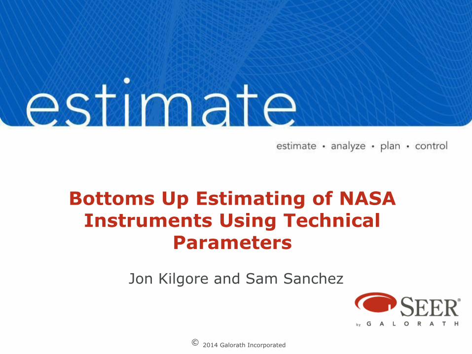
Bottoms Up Estimating of NASA Instruments Using Technical
Parameters
Jon Kilgore and Sam Sanchez
© 2014 Galorath Incorporated
About Galorath
Galorath’s consultants and SEER products help clients estimate effort, duration, cost, and gauge risk
• Over 30 years in business conducting mil/aero cost research
• Hundreds of customers, many Fortune 500
• Small business (NAICS 541330, 541511, 541611, 541712)
• Professional services organization provides consulting and training
• Supporting NASA with ~15 cost estimators
• Over 100 unique instruments estimated for NASA during the last 2-3 years
• A software publisher / research firm with four flagship products:
2
© 2014 Galorath Incorporated
Background – Estimating with Technical Parameters • Our research into the relationships between
technical parameters and cost began more than 10 years ago (first released Spyglass during December 2004)
• Two areas where we have achieved greatest maturity:
• Electro-optical systems in Space, Aircraft, and Missile platforms
• Integrated Circuits (printed circuit boards, FPGAs and ASICs)
• Our methodology utilizes 3 to 8 Key Technical/ Performance Parameters (KTPPs) for each technology (i.e., device or process) estimated
• Applying quantitative analysis that simultaneously solves capability vs. cost assessments
• Estimates at the component and assembly levels
3
© 2014 Galorath Incorporated
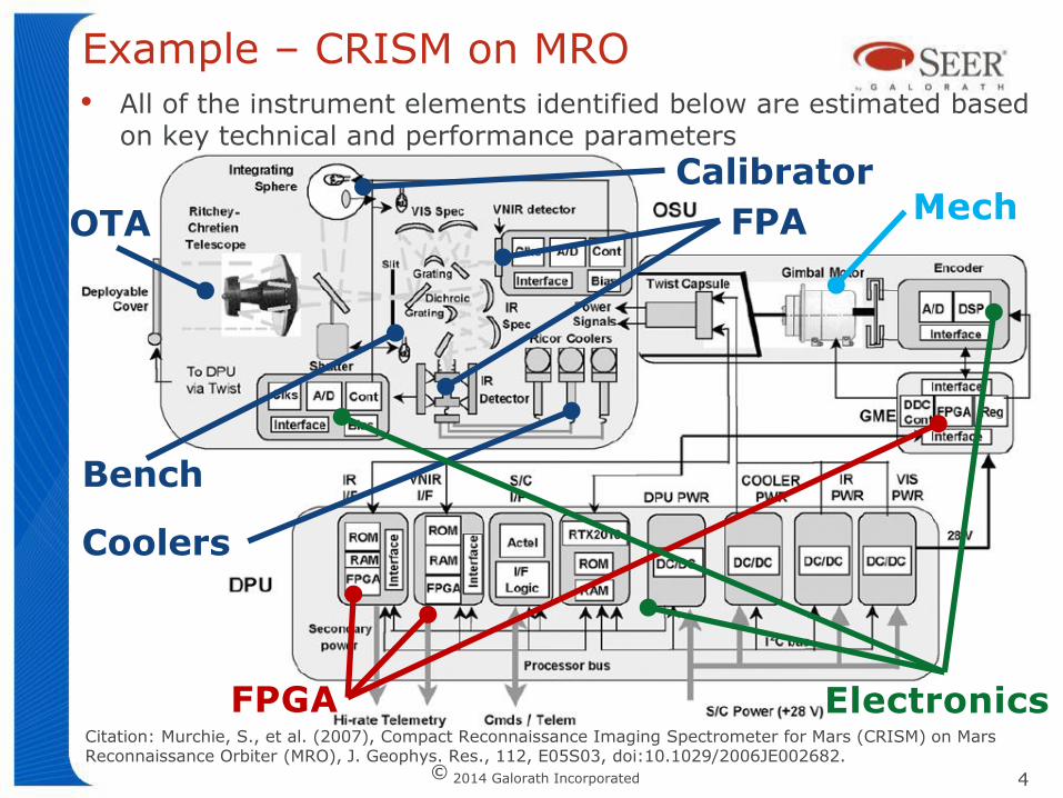
• All of the instrument elements identified below are estimated based on key technical and performance parameters
Example – CRISM on MRO
OTA
Calibrator
Coolers
FPA
Bench
Citation: Murchie, S., et al. (2007), Compact Reconnaissance Imaging Spectrometer for Mars (CRISM) on Mars Reconnaissance Orbiter (MRO), J. Geophys. Res., 112, E05S03, doi:10.1029/2006JE002682.
4
Mech
Electronics FPGA
© 2014 Galorath Incorporated
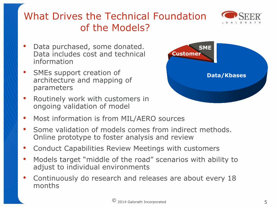
What Drives the Technical Foundation of the Models?
SME
Data/Kbases
Customer • Data purchased, some donated.
Data includes cost and technical information
• SMEs support creation of architecture and mapping of parameters
• Routinely work with customers in ongoing validation of model
• Most information is from MIL/AERO sources
• Some validation of models comes from indirect methods. Online prototype to foster analysis and review
• Conduct Capabilities Review Meetings with customers
• Models target “middle of the road” scenarios with ability to adjust to individual environments
• Continuously do research and releases are about every 18 months
5
© 2014 Galorath Incorporated
Subject Matter Experts
• Galorath augments its staff with external technical SMEs
• Program Director (Ford/Loral) – 35 years experience in managing space programs
• Program Manager (Perkin Elmer) – 32 years experience in managing EOS programs for space applications
• Product Line Director (Honeywell/Bendix Space Systems) – 27 years experience in mechanisms for space applications
• Senior Scientist (Barnes Engineering/EDO/Goodrich) – 30 years developing electro-optical systems for commercial and space applications
• Product Line Manager/Business Development (Honeywell/SAIC) – 25 years development of advanced IR focal plane arrays and related business development
• Chief Engineer (Honeywell Space Systems) – 16 years development of advanced mechanisms and control systems
6
© 2014 Galorath Incorporated
ESTIMATING ELECTRO-OPTICAL SENSORS UTILIZING KTTPS
© 2014 Galorath Incorporated
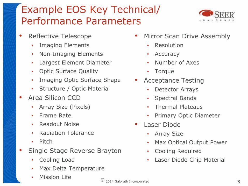
Example EOS Key Technical/ Performance Parameters
• Reflective Telescope
• Imaging Elements
• Non-Imaging Elements
• Largest Element Diameter
• Optic Surface Quality
• Imaging Optic Surface Shape
• Structure / Optic Material
• Area Silicon CCD
• Array Size (Pixels)
• Frame Rate
• Readout Noise
• Radiation Tolerance
• Pitch
• Single Stage Reverse Brayton
• Cooling Load
• Max Delta Temperature
• Mission Life
• Mirror Scan Drive Assembly
• Resolution
• Accuracy
• Number of Axes
• Torque
• Acceptance Testing
• Detector Arrays
• Spectral Bands
• Thermal Plateaus
• Primary Optic Diameter
• Laser Diode
• Array Size
• Max Optical Output Power
• Cooling Required
• Laser Diode Chip Material
8

© 2014 Galorath Incorporated
• We will examine the telescope, optical bench and a detector in more detail
Example – Compact Reconnaissance Imaging Spectrometer for Mars
Citation: Murchie, S., et al. (2007), Compact Reconnaissance Imaging Spectrometer for Mars (CRISM) on Mars Reconnaissance Orbiter (MRO), J. Geophys. Res., 112, E05S03, doi:10.1029/2006JE002682.
9
© 2014 Galorath Incorporated
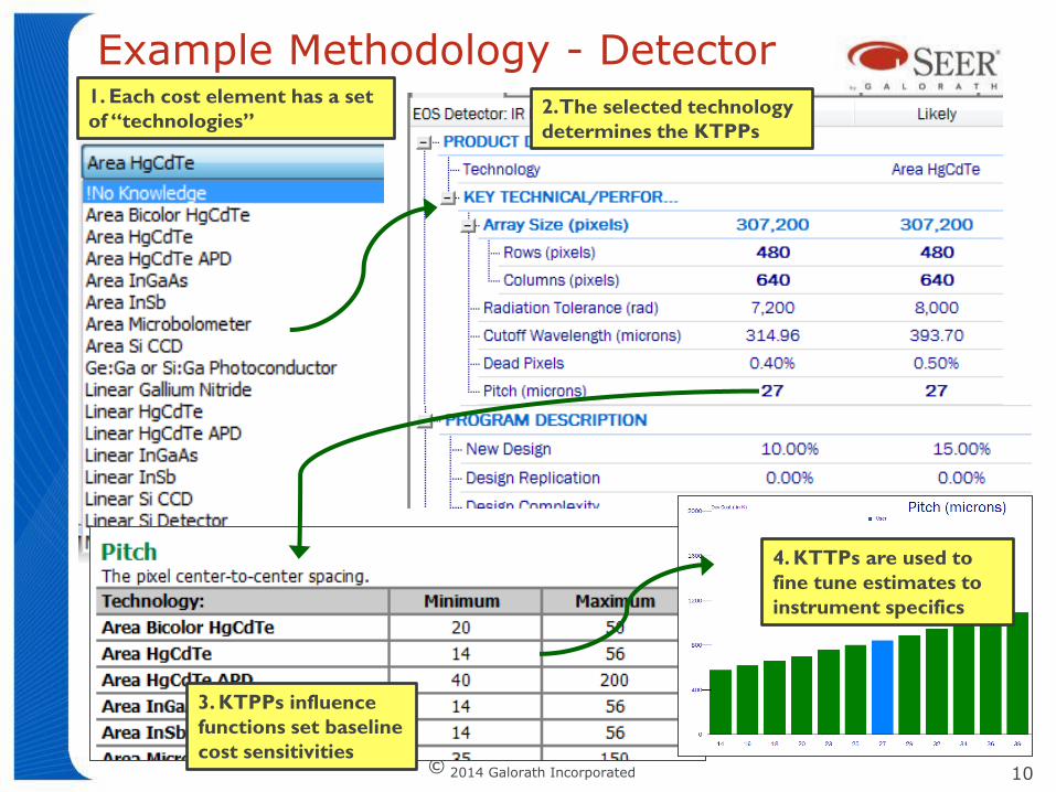
Example Methodology - Detector 1. Each cost element has a set
of “technologies” 2. The selected technology
determines the KTPPs
10
3. KTPPs influence
functions set baseline
cost sensitivities
4. KTTPs are used to
fine tune estimates to
instrument specifics
© 2014 Galorath Incorporated
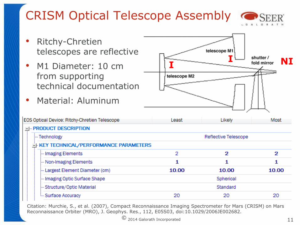
CRISM Optical Telescope Assembly
NI I I
Citation: Murchie, S., et al. (2007), Compact Reconnaissance Imaging Spectrometer for Mars (CRISM) on Mars Reconnaissance Orbiter (MRO), J. Geophys. Res., 112, E05S03, doi:10.1029/2006JE002682.
11
• Ritchy-Chretien telescopes are reflective
• M1 Diameter: 10 cm from supporting technical documentation
• Material: Aluminum
© 2014 Galorath Incorporated
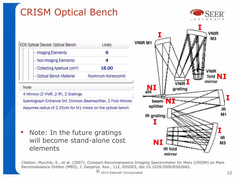
CRISM Optical Bench
• Note: In the future gratings will become stand-alone cost elements
NI
NI
NI
NI
I I
I
I I
I
Citation: Murchie, S., et al. (2007), Compact Reconnaissance Imaging Spectrometer for Mars (CRISM) on Mars Reconnaissance Orbiter (MRO), J. Geophys. Res., 112, E05S03, doi:10.1029/2006JE002682.
12
© 2014 Galorath Incorporated
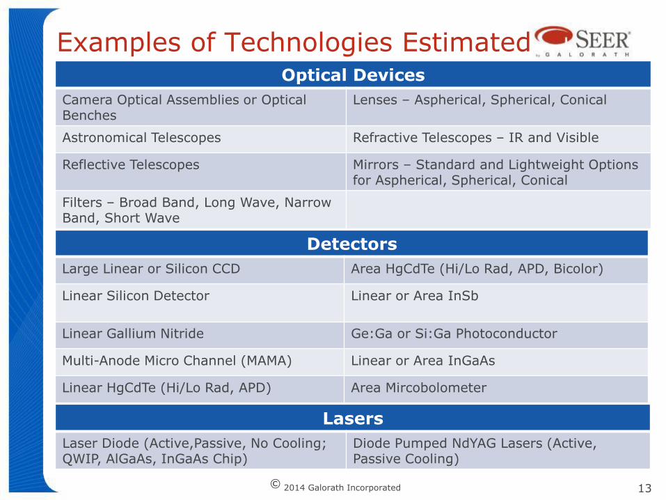
Examples of Technologies Estimated Optical Devices
Camera Optical Assemblies or Optical Benches
Lenses – Aspherical, Spherical, Conical
Astronomical Telescopes Refractive Telescopes – IR and Visible
Reflective Telescopes Mirrors – Standard and Lightweight Options for Aspherical, Spherical, Conical
Filters – Broad Band, Long Wave, Narrow Band, Short Wave
Detectors
Large Linear or Silicon CCD Area HgCdTe (Hi/Lo Rad, APD, Bicolor)
Linear Silicon Detector Linear or Area InSb
Linear Gallium Nitride Ge:Ga or Si:Ga Photoconductor
Multi-Anode Micro Channel (MAMA) Linear or Area InGaAs
Linear HgCdTe (Hi/Lo Rad, APD) Area Mircobolometer
Lasers
Laser Diode (Active,Passive, No Cooling; QWIP, AlGaAs, InGaAs Chip)
Diode Pumped NdYAG Lasers (Active, Passive Cooling)
13
© 2014 Galorath Incorporated
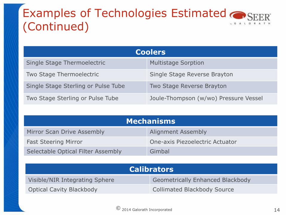
Coolers
Single Stage Thermoelectric Multistage Sorption
Two Stage Thermoelectric Single Stage Reverse Brayton
Single Stage Sterling or Pulse Tube Two Stage Reverse Brayton
Two Stage Sterling or Pulse Tube Joule-Thompson (w/wo) Pressure Vessel
Mechanisms
Mirror Scan Drive Assembly Alignment Assembly
Fast Steering Mirror One-axis Piezoelectric Actuator
Selectable Optical Filter Assembly Gimbal
Calibrators
Visible/NIR Integrating Sphere Geometrically Enhanced Blackbody
Optical Cavity Blackbody Collimated Blackbody Source
Examples of Technologies Estimated (Continued)
14
© 2014 Galorath Incorporated
ESTIMATING INTEGRATED CIRCUITS & ELECTRONICS UTILIZING KTTPS
© 2014 Galorath Incorporated
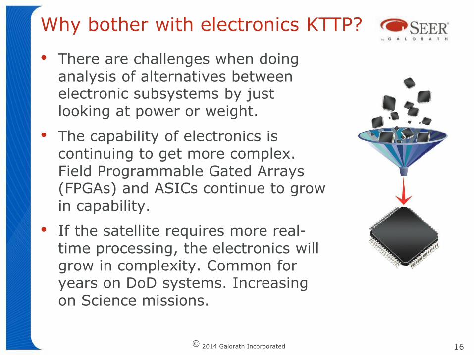
Why bother with electronics KTTP?
• There are challenges when doing analysis of alternatives between electronic subsystems by just looking at power or weight.
• The capability of electronics is continuing to get more complex. Field Programmable Gated Arrays (FPGAs) and ASICs continue to grow in capability.
• If the satellite requires more real-time processing, the electronics will grow in complexity. Common for years on DoD systems. Increasing on Science missions.
16
© 2014 Galorath Incorporated
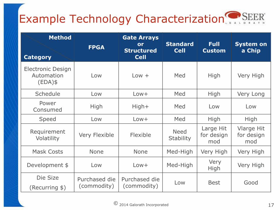
Example Technology Characterization
Method
Category
FPGA
Gate Arrays or
Structured Cell
Standard Cell
Full Custom
System on a Chip
Electronic Design Automation
(EDA)$ Low Low + Med High Very High
Schedule Low Low+ Med High Very Long
Power Consumed
High High+ Med Low Low
Speed Low Low+ Med High High
Requirement Volatility
Very Flexible Flexible Need
Stability
Large Hit for design
mod
Vlarge Hit for design
mod
Mask Costs None None Med-High Very High Very High
Development $ Low Low+ Med-High Very High
Very High
Die Size
(Recurring $)
Purchased die (commodity)
Purchased die (commodity)
Low Best Good
17
© 2014 Galorath Incorporated
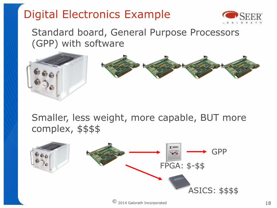
Digital Electronics Example
Smaller, less weight, more capable, BUT more complex, $$$$
Standard board, General Purpose Processors (GPP) with software
FPGA: $-$$
ASICS: $$$$
GPP
18
© 2014 Galorath Incorporated
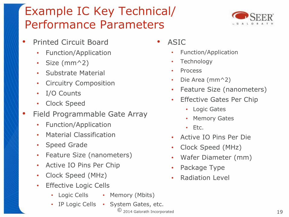
Example IC Key Technical/ Performance Parameters
• Printed Circuit Board
• Function/Application
• Size (mm^2)
• Substrate Material
• Circuitry Composition
• I/O Counts
• Clock Speed
• Field Programmable Gate Array
• Function/Application
• Material Classification
• Speed Grade
• Feature Size (nanometers)
• Active IO Pins Per Chip
• Clock Speed (MHz)
• Effective Logic Cells
• Logic Cells
• IP Logic Cells
• ASIC
• Function/Application
• Technology
• Process
• Die Area (mm^2)
• Feature Size (nanometers)
• Effective Gates Per Chip
• Logic Gates
• Memory Gates
• Etc.
• Active IO Pins Per Die
• Clock Speed (MHz)
• Wafer Diameter (mm)
• Package Type
• Radiation Level
• Memory (Mbits)
• System Gates, etc.
19
© 2014 Galorath Incorporated
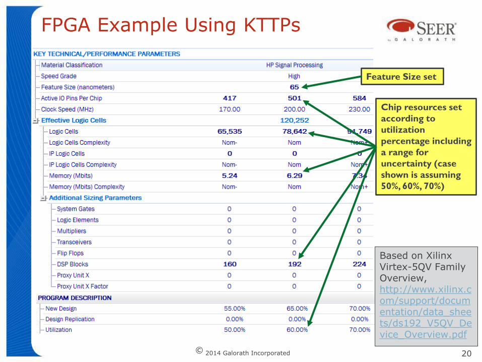
FPGA Example Using KTTPs
20
Feature Size set
Chip resources set
according to
utilization
percentage including
a range for
uncertainty (case
shown is assuming
50%, 60%, 70%)
Based on Xilinx Virtex-5QV Family Overview, http://www.xilinx.com/support/documentation/data_sheets/ds192_V5QV_Device_Overview.pdf
© 2014 Galorath Incorporated
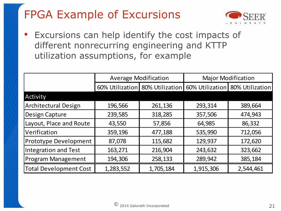
FPGA Example of Excursions
21
• Excursions can help identify the cost impacts of different nonrecurring engineering and KTTP utilization assumptions, for example
60% Utilization 80% Utilization 60% Utilization 80% Utilization
Activity
Architectural Design 196,566 261,136 293,314 389,664
Design Capture 239,585 318,285 357,506 474,943
Layout, Place and Route 43,550 57,856 64,985 86,332
Verification 359,196 477,188 535,990 712,056
Prototype Development 87,078 115,682 129,937 172,620
Integration and Test 163,271 216,904 243,632 323,662
Program Management 194,306 258,133 289,942 385,184
Total Development Cost 1,283,552 1,705,184 1,915,306 2,544,461
Average Modification Major Modification
© 2014 Galorath Incorporated
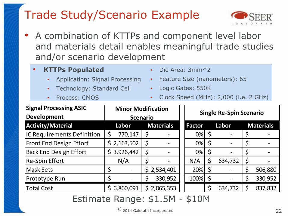
Trade Study/Scenario Example
• A combination of KTTPs and component level labor and materials detail enables meaningful trade studies and/or scenario development
22
Estimate Range: $1.5M - $10M
• KTTPs Populated
• Application: Signal Processing
• Technology: Standard Cell
• Process: CMOS
• Die Area: 3mm^2
• Feature Size (nanometers): 65
• Logic Gates: 550K
• Clock Speed (MHz): 2,000 (i.e. 2 GHz)
Signal Processing ASIC
Development
Activity/Material Labor Materials Factor Labor Materials
IC Requirements Definition 770,147$ -$ 0% -$ -$
Front End Design Effort 2,163,502$ -$ 0% -$ -$
Back End Design Effort 3,926,442$ -$ 0% -$ -$
Re-Spin Effort N/A -$ N/A 634,732$ -$
Mask Sets -$ 2,534,401$ 20% -$ 506,880$
Prototype Run -$ 330,952$ 100% -$ 330,952$
Total Cost 6,860,091$ 2,865,353$ 634,732$ 837,832$
Single Re-Spin ScenarioMinor Modification
Scenario
© 2014 Galorath Incorporated
Validation
• Continually doing validation with our customers. Even when data is not provided, we receive feedback on cost outputs and parameter weight/sensitivity
• Supports understanding on how component level modeling could be done better or identify new key technical parameters
• Customers champions also support the creation of new Knowledge base defaults.
• Formal validation of model based on specific cost data. Must have solid understanding of not only the cost output but also what drove it (technically, programmatically, etc.). Cost forensics.
23
© 2014 Galorath Incorporated
Challenges
• Technical understanding to interpret diagrams and associated narratives at the component level
• Lack of a Master Equipment List and/or detailed diagrams significantly impacts modeling accuracy. The models do not readily support system or subsystem level estimating.
• Technical parameters are not always given and the analyst must calculate or derive these values
• Component/assembly level estimating requires more time and effort than top-down approaches
• Reliance on strong industry/developer relationships because Government data is frequently high level
• Technical characterization of the tremendous variety of science sensors and instrumentation
24
© 2014 Galorath Incorporated
What We Are Working On Now
• 2nd formal model validation study with NASA
• Mass Spectrometers
• Particle Counters
• Cubesats
• Platform-driven cost impacts (e.g. ISS)
• Gratings as individual cost elements
• Cross delay line (XDL) detectors
• Micro-channel plate (MCP) detectors
• EOS cost impact of X-ray and gamma ray wavelength missions
• Laser spectroscopy
25
© 2014 Galorath Incorporated
Contact Information:
www.galorath.com
Dan Galorath [email protected] 310-414-3222, ext. 614
Sam Sanchez [email protected] 919-803-8165
Jon Kilgore [email protected] 703-429-2403
26