Embed Size (px)
Citation preview

Industrial battery monitors:BQ76942 / BQ76952 device overview

BQ76942 / BQ76952 features•Digital voltage, current, and temperature measurements, integrated coulomb counter Monitoring•Primary protection for OV, UV, OTC, OTD, UTC, UTD, OTF, OW, SCD, OCD1,2,3, OCC, cell balancing, watchdog, and more. Integrated secondary protection.Protections
• Integrated charge pump & drivers for high-side protection NFETsFET drivers•Integrated passive cell balancing up to 50mA, support for external passive balancingCell balancing•Support for high-side PFET-based precharge and predischarge modesPrechg / Predsg•Dual LDOs programmable as 5V / 3.3V / 3.0V / 2.5V / 1.8V, up to 45mA eachIntegrated LDOs•Support for I2C, SPI, & HDQ interfacesCommunications•High voltage tolerance of 85V absolute maximum on select pinsHigh voltage tolerance
BQ76942 / BQ76952 feature highlights
Protection redundancy
Standalone HW based protection
Autonomous or host controlled recovery
Accurate & advanced pack measurement
ADC accuracy @ +/-10mV over 0C – 60C
Fast data refresh rate 22.5ms to 63ms
Synchronized V/I measurement
Separate Coulomb Counter for continuous current measurement
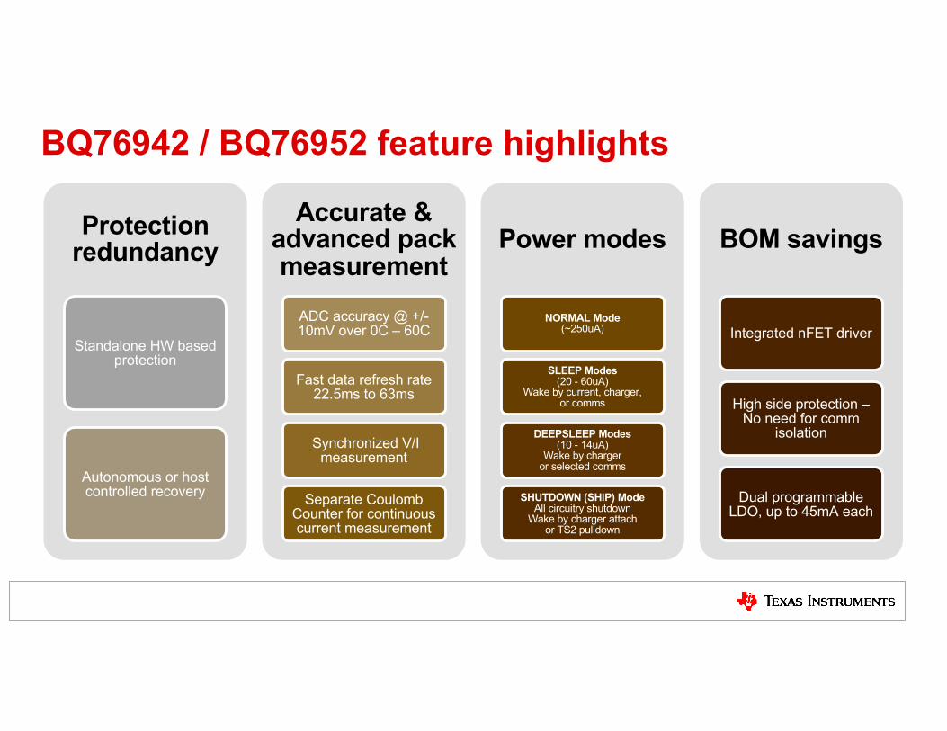
Power modes
NORMAL Mode(~250uA)
SLEEP Modes(20 - 60uA)
Wake by current, charger, or comms
DEEPSLEEP Modes(10 - 14uA)
Wake by charger or selected comms
SHUTDOWN (SHIP) ModeAll circuitry shutdown
Wake by charger attach or TS2 pulldown
BOM savings
Integrated nFET driver
High side protection –No need for comm
isolation
Dual programmable LDO, up to 45mA each

BQ769423S - 10S monitor + protector block diagram

BQ769523S - 16S monitor + protector block diagram

BQ76952: 16S simplified schematic

Programmable REG1 and REG2 (1.8V / 2.5V / 3.0V / 3.3V / 5V) e.g., to power CAN transceiver or MCU
BQ76952: 16S simplified schematic

Programmable REG1 and REG2 (1.8V / 2.5V / 3.0V / 3.3V / 5V) e.g., to power CAN transceiver or MCU
Integrated high-side NFET drivers
BQ76952: 16S simplified schematic

Programmable REG1 and REG2 (1.8V / 2.5V / 3.0V / 3.3V / 5V) e.g., to power CAN transceiver or MCU
Integrated high-side NFET drivers
Integrated PFET driverse.g. to slowly charge up the capacitive load at system startup
BQ76952: 16S simplified schematic

Programmable REG1 and REG2 (1.8V / 2.5V / 3.0V / 3.3V / 5V) e.g., to power CAN transceiver or MCU
Integrated high-side NFET drivers
Integrated PFET driverse.g. to slowly charge up the capacitive load at system startup
Secondary protection.Works with external secondary protector
BQ76952: 16S simplified schematic

Programmable REG1 and REG2 (1.8V / 2.5V / 3.0V / 3.3V / 5V) e.g., to power CAN transceiver or MCU
Integrated high-side NFET drivers
Integrated PFET driverse.g. to slowly charge up the capacitive load at system startup
Integrated CB FETs Up to 50mA CB current
Secondary protection.Works with external secondary protector
Random cell attach orderHigh voltage tolerance
on cell Input pins
BQ76952: 16S simplified schematic

Programmable REG1 and REG2 (1.8V / 2.5V / 3.0V / 3.3V / 5V) e.g., to power CAN transceiver or MCU
Integrated high-side NFET drivers
Integrated PFET driverse.g. to slowly charge up the capacitive load at system startup
Integrated CB FETs Up to 50mA CB current
Digital CHG and DSG outputCan use as alternative
charge/discharge fault signal
Secondary protection.Works with external secondary protector
Random cell attach orderHigh voltage tolerance
on cell Input pins
BQ76952: 16S simplified schematic

Programmable REG1 and REG2 (1.8V / 2.5V / 3.0V / 3.3V / 5V) e.g., to power CAN transceiver or MCU
Integrated high-side NFET drivers
Integrated PFET driverse.g. to slowly charge up the capacitive load at system startup
External HW shutdown orreset control and fast FETOFF control
Integrated CB FETs Up to 50mA CB current
Digital CHG and DSG outputCan use as alternative
charge/discharge fault signal
Secondary protection.Works with external secondary protector
Random cell attach orderHigh voltage tolerance
on cell Input pins
BQ76952: 16S simplified schematic

Programmable REG1 and REG2 (1.8V / 2.5V / 3.0V / 3.3V / 5V) e.g., to power CAN transceiver or MCU
Integrated high-side NFET drivers
Integrated PFET driverse.g. to slowly charge up the capacitive load at system startup
I2C or HDQ or SPI
External HW shutdown orreset control and fast FETOFF control
Integrated CB FETs Up to 50mA CB current
Digital CHG and DSG outputCan use as alternative
charge/discharge fault signal
Secondary protection.Works with external secondary protector
Random cell attach orderHigh voltage tolerance
on cell Input pins
BQ76952: 16S simplified schematic
BQ76942 / BQ76952 power modes•All protections enabled•DFET & CFET on•Regular voltage, current, and temperature measurements
•LDO programmable
NORMAL Mode~250uA
•Most protections still enabled•DFET on (multiple modes), CFET off•ADC intermittent, CC in current wake detect mode•LDO programmable (can keep MCU powered)•Wake by current / comm / charger / reset
SLEEP Mode20 – 60uA
•Most circuits off, FETs off •No ADC/CC, no protection•LDO programmable (can keep MCU powered)•Wake by selected comms / charger / reset signal
DEEPSLEEP Mode10 – 14uA
•All circuitry off (except wakeup detector)•No measurements, no protections•LDO powered off•Wake by pulling TS2 to and / or charger attach
SHUTDOWN Mode<1uA
• Optimized for system idle state• MCU can be in low power mode without
compromising safety• V / I / T data collected periodically
System Benefit
Different power modes meeting different system needs
• Lowest power mode for shipping, storage, or long-term power-down
• Optimized for system low power state• Lowest power mode while still providing
LDO operation to keep MCU powered
• Highest performance for system active state• Full protections, V / I / T data collected
continuously

• External NPN drops voltage from top-of-stack level to ~5.5V pre-regulator level (REGIN)
• REG1 and REG2 draw input from REGIN, provide programmable outputs from 1.8V to 5.0V.
• Includes option for customer to provide REGIN from external DC/DC.
BQ76942 / BQ76952Programmable Dual LDO

BQ76942 / BQ76952 protections
Function Range Delay Recovery Method (Standalone mode)
Voltage COV 1.0V – 5.5V, 50mV steps 10ms ~ 6762ms, 3.3ms steps Voltage hysteresis (100mV, 200mV)
CUV 1.0V – 4V, 50mV steps 10ms ~ 6762ms, 3.3ms steps Voltage hysteresis (100mV, 200mV) and/or load removal
Current OCC 4mV – 124mV, 2mV steps 10ms ~ 426ms Load attach and/or delay
OCD1/2 -4mV – -200mV, 2mV steps 10ms ~ 426ms Load removal and/or delay
OCD3 -32768 – -4000-userA, 1-userA steps
1s ~ 255s Load removal and/or delay
SCD 10mV ~ 500mV 8us, 15us ~ 450us, 15us steps Load removal and/or delay
OVL, OCDL, SCDL Various Various Delay & more
• Protection through combination of comparators and ADC • Support for MCU mode (recovery by MCU control), Standalone mode (auto-recovery)• Fault signal interrupt to MCU• OTP programmable default protection setting

BQ76942 / BQ76952 protectionsFunction Range Delay Recovery Method (Standalone mode)
Temperature OTC -40C – 120C, 1C steps 1s ~ 255s Temperature recovery threshold -40C ~ 120C, 1C steps
OTD -40C – 120C, 1C steps 1s ~ 255s Temperature recovery threshold -40C ~ 120C, 1C steps
UTC -40C – 120C, 1C steps 1s ~ 255s Temperature recovery threshold -40C ~ 120C, 1C steps
UTD -40C – 120C, 1C steps 1s ~ 255s Temperature recovery threshold -40C ~ 120C, 1C steps
UTINT -40C – 120C, 1C steps 1s ~ 255s Temperature recovery threshold -40C ~ 120C, 1C steps
OTINT -40C – 120C, 1C steps 1s ~ 255s Temperature recovery threshold -40C ~ 120C, 1C steps
OTF 0C – 150C, 1C steps 1s ~ 255s Temperature recovery threshold 0C ~ 150C, 1C steps
HostWatchdog
HWP 1s ~ 65535s Valid communications occurs
Pre-charge Timeout
PTO 1s ~ 65535s Pre-charge ends when timeout occurs

BQ76942 / BQ76952 permanent fail
Function Range Delay
Cell Open Wire COW Programmable check interval, triggers SOV/SUV 1s ~ 255s
Charge FET Fail CFETF 10mA ~ 5000mA charging while CFET driven off 1s ~ 255s
Discharge FET Fail DFETF -10mA ~ -5000mA discharging while DFET driven off 1s ~ 255s
Second Level Fail 2LVLF Detects fuse drive 1s ~ 255s
Voltage SOV 1mV – 32767mV, 1mV steps 1s ~ 255s
SUV 1mV – 32767mV, 1mV steps 1s ~ 255s
Current SOCC 1-userA ~ 32767-userA (userA can be 0.1 / 1 / 10 / 100mA ) 1s ~ 255s
SOCD -32767-userA ~ -1-userA 1s ~ 255s
Temperature SOTC -40C – 120C, 1C steps 1s ~ 255s
SOTF 0C – 150C, 1C steps 1s ~ 255s
Voltage Imbalance VIMR 1mV ~ 5500mV 1s ~ 255s
VIMA 1mV ~ 5500mV 1s ~ 255s
OTP Memory Signature OTPF
Various diagnostics Stuck mux checks, internal oscillator check, Cu deposition, stack vs cell voltage check, etc.
• Programmable options to trigger fuse• OTP programmable default protection setting

48