Embed Size (px)
Citation preview
BME-MITFPGA labor
Brief Introduction to Verilog HDL(Part 2)
BUDAPEST UNIVERSITY OF TECHNOLOGY AND ECONOMICSFACULTY OF ELECTRICAL ENGINEERING AND INFORMATICS
DEPARTMENT OF MEASUREMENT AND INFORMATION SYSTEMS
Tamás RaikovichBUTE DMIS
BME-MITFPGA labor
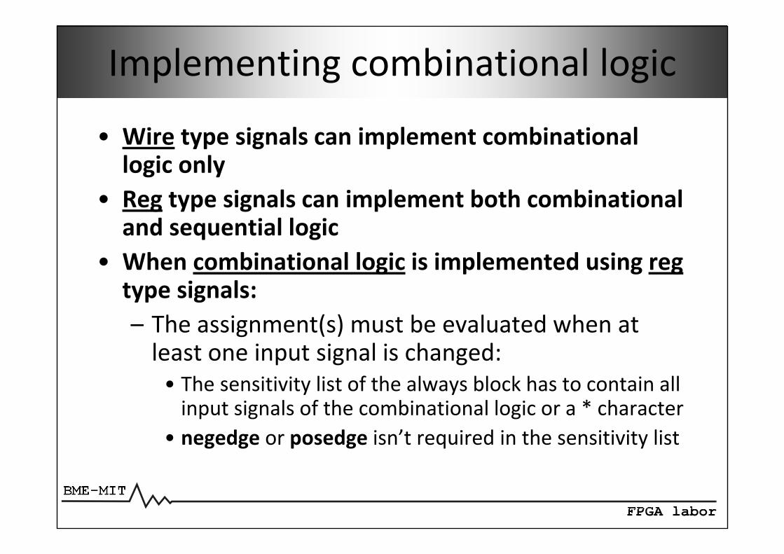
Implementing combinational logic
• Wire type signals can implement combinational logic only
• Reg type signals can implement both combinational and sequential logic
• When combinational logic is implemented using regtype signals:– The assignment(s) must be evaluated when at least one input signal is changed:• The sensitivity list of the always block has to contain all input signals of the combinational logic or a * character
• negedge or posedge isn’t required in the sensitivity list
BME-MITFPGA labor
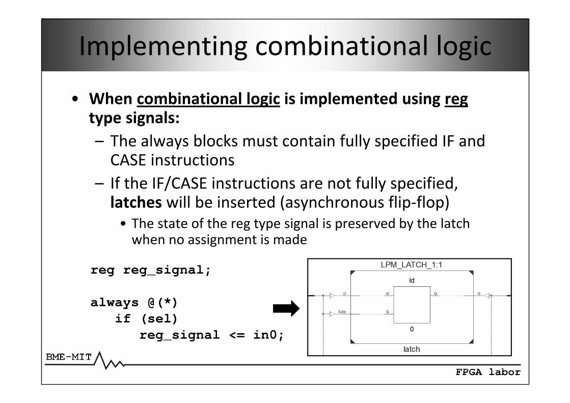
Implementing combinational logic
• When combinational logic is implemented using regtype signals:– The always blocks must contain fully specified IF and CASE instructions
– If the IF/CASE instructions are not fully specified, latches will be inserted (asynchronous flip‐flop)• The state of the reg type signal is preserved by the latch when no assignment is made
reg reg_signal;
always @(*)if (sel)
reg_signal <= in0;
BME-MITFPGA labor
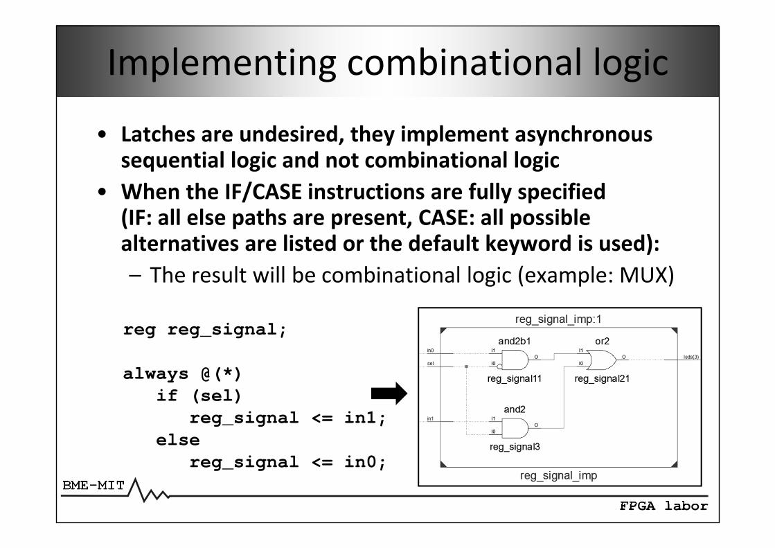
Implementing combinational logic
• Latches are undesired, they implement asynchronous sequential logic and not combinational logic
• When the IF/CASE instructions are fully specified(IF: all else paths are present, CASE: all possible alternatives are listed or the default keyword is used):– The result will be combinational logic (example: MUX)
reg reg_signal;
always @(*)if (sel)
reg_signal <= in1;else
reg_signal <= in0;
BME-MITFPGA labor
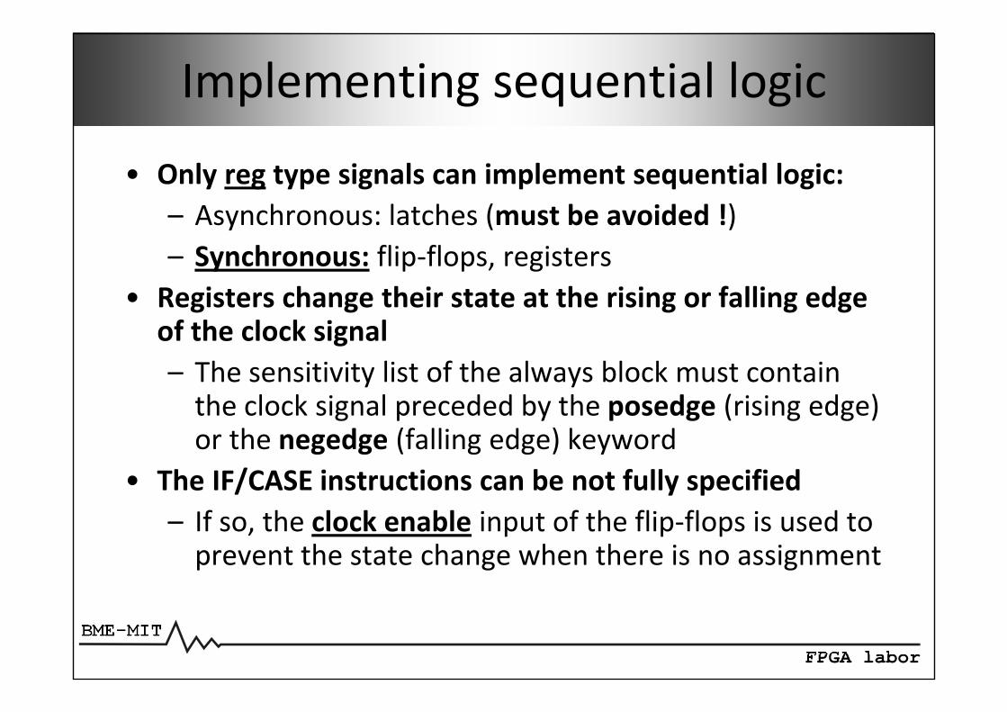
Implementing sequential logic
• Only reg type signals can implement sequential logic:– Asynchronous: latches (must be avoided !)– Synchronous: flip‐flops, registers
• Registers change their state at the rising or falling edge of the clock signal– The sensitivity list of the always block must contain the clock signal preceded by the posedge (rising edge) or the negedge (falling edge) keyword
• The IF/CASE instructions can be not fully specified– If so, the clock enable input of the flip‐flops is used to prevent the state change when there is no assignment
BME-MITFPGA labor
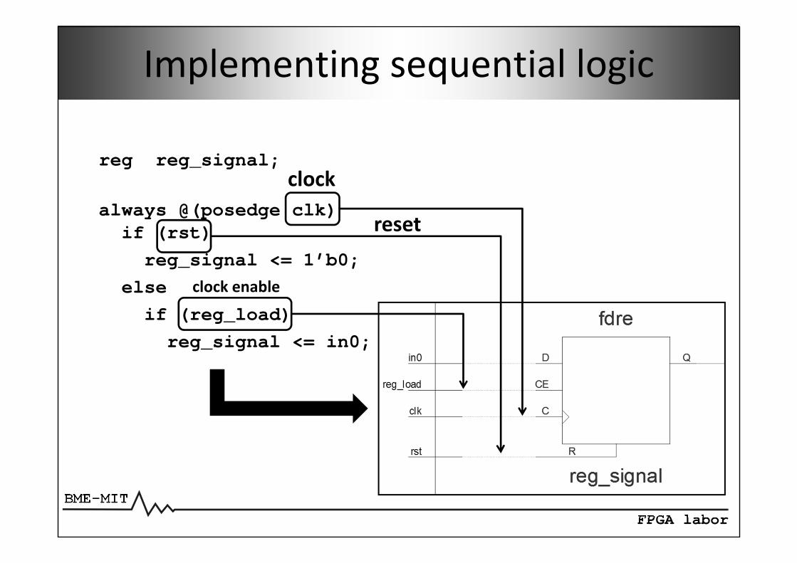
Implementing sequential logic
reg reg_signal;
always @(posedge clk)if (rst)
reg_signal <= 1’b0;else
if (reg_load)reg_signal <= in0;
clock
reset
clock enable
BME-MITFPGA labor
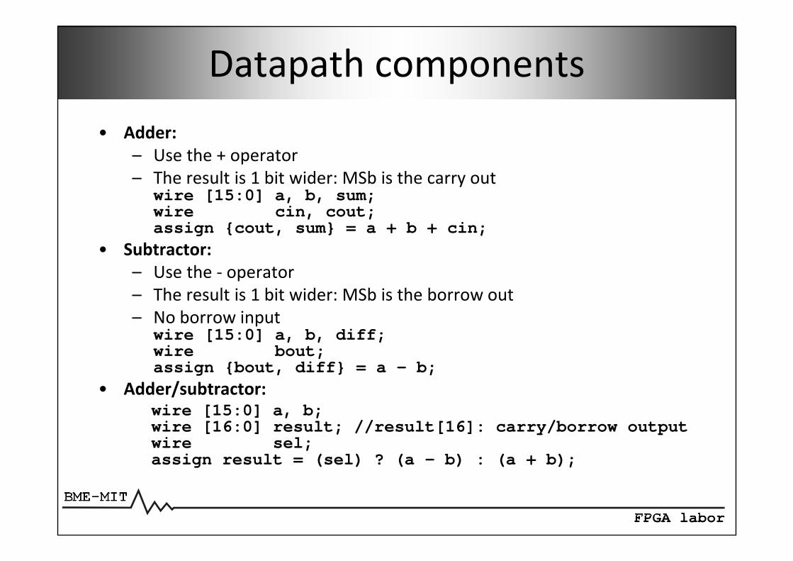
Datapath components• Adder:
– Use the + operator– The result is 1 bit wider: MSb is the carry out
wire [15:0] a, b, sum;wire cin, cout;assign {cout, sum} = a + b + cin;
• Subtractor: – Use the ‐ operator– The result is 1 bit wider: MSb is the borrow out– No borrow input
wire [15:0] a, b, diff;wire bout;assign {bout, diff} = a - b;
• Adder/subtractor:wire [15:0] a, b;wire [16:0] result; //result[16]: carry/borrow outputwire sel;assign result = (sel) ? (a – b) : (a + b);
BME-MITFPGA labor
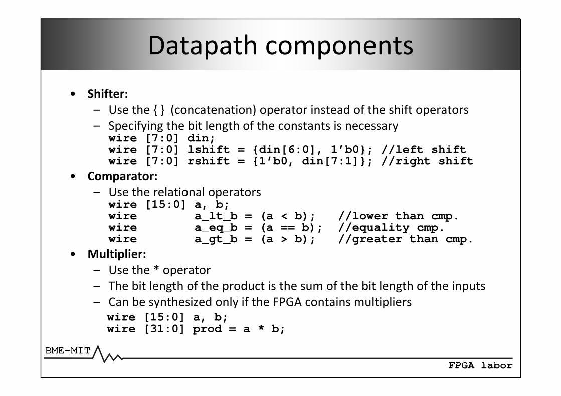
Datapath components• Shifter:
– Use the { } (concatenation) operator instead of the shift operators– Specifying the bit length of the constants is necessary
wire [7:0] din;wire [7:0] lshift = {din[6:0], 1’b0}; //left shiftwire [7:0] rshift = {1’b0, din[7:1]}; //right shift
• Comparator: – Use the relational operators
wire [15:0] a, b;wire a_lt_b = (a < b); //lower than cmp.wire a_eq_b = (a == b); //equality cmp.wire a_gt_b = (a > b); //greater than cmp.
• Multiplier:– Use the * operator– The bit length of the product is the sum of the bit length of the inputs– Can be synthesized only if the FPGA contains multiplierswire [15:0] a, b;wire [31:0] prod = a * b;
BME-MITFPGA labor
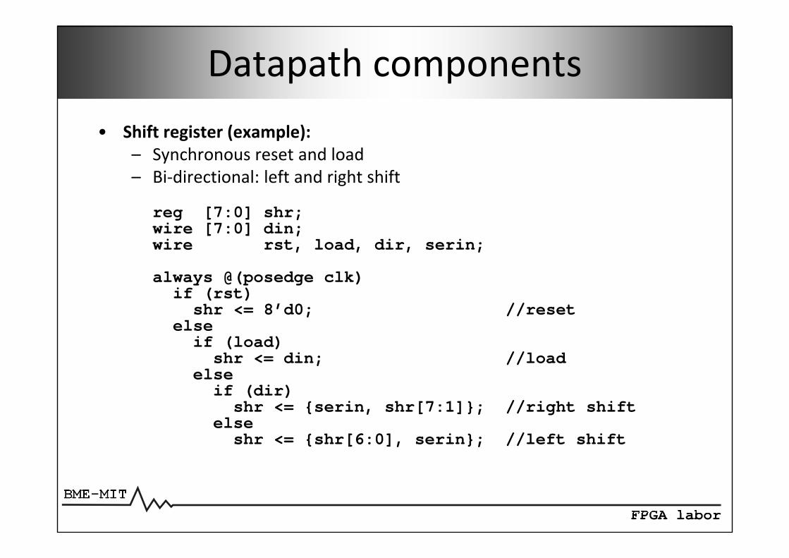
Datapath components• Shift register (example):
– Synchronous reset and load– Bi‐directional: left and right shift
reg [7:0] shr;wire [7:0] din;wire rst, load, dir, serin;
always @(posedge clk)if (rst)shr <= 8’d0; //reset
elseif (load)shr <= din; //load
elseif (dir)shr <= {serin, shr[7:1]}; //right shift
elseshr <= {shr[6:0], serin}; //left shift
BME-MITFPGA labor
Datapath components• Counter (example):
– Synchronous reset and load– Bi‐directional: up/down counter
reg [8:0] cnt;wire [8:0] din;wire rst, load, dir;wire tc = (dir) ? (cnt==9’d0) : (cnt==9’d511);
always @(posedge clk)if (rst)cnt <= 9’d0; //reset
elseif (load)cnt <= din; //load
elseif (dir)cnt <= cnt – 9’d1; //down count
elsecnt <= cnt + 9’d1; //up count
BME-MITFPGA labor
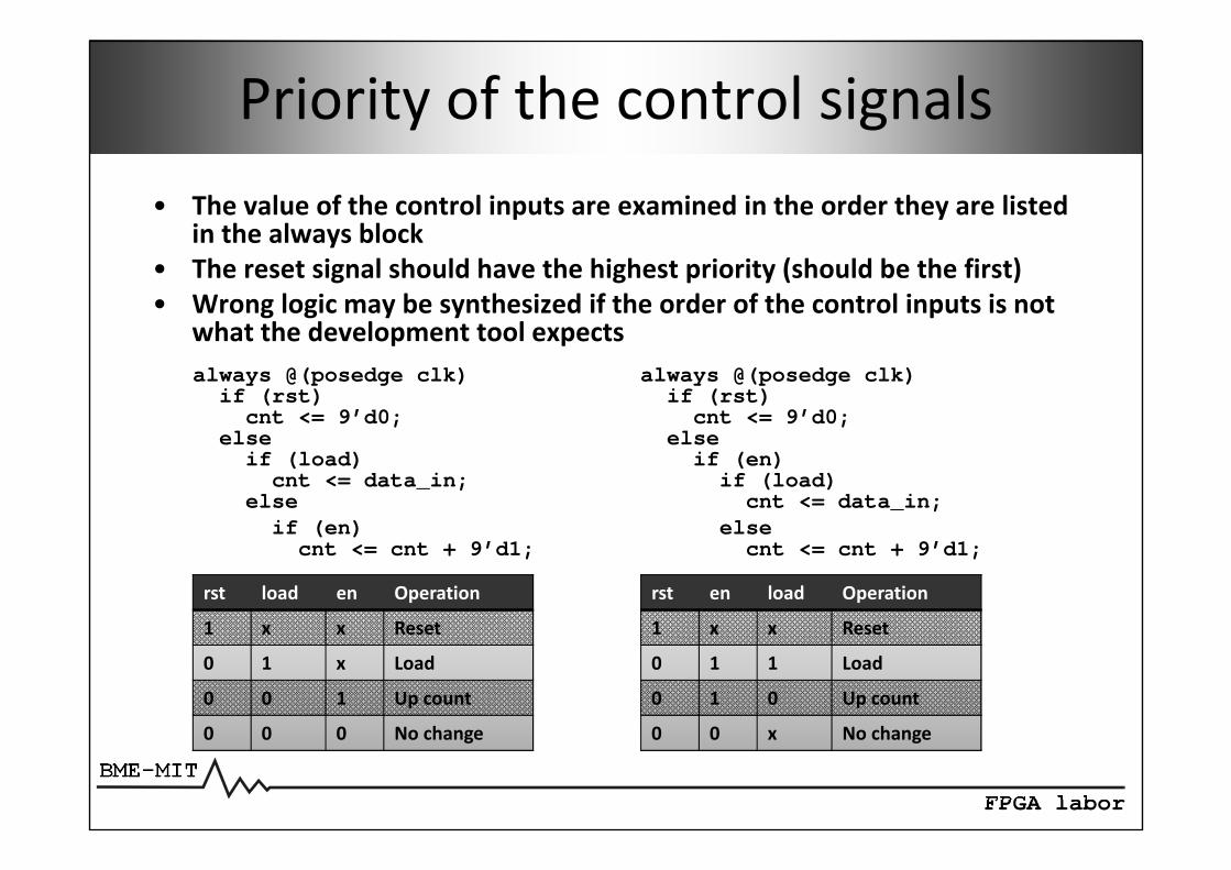
Priority of the control signals• The value of the control inputs are examined in the order they are listed
in the always block• The reset signal should have the highest priority (should be the first)• Wrong logic may be synthesized if the order of the control inputs is not
what the development tool expectsalways @(posedge clk) always @(posedge clk)if (rst) if (rst)cnt <= 9’d0; cnt <= 9’d0;
else elseif (load) if (en)cnt <= data_in; if (load)
else cnt <= data_in;if (en) elsecnt <= cnt + 9’d1; cnt <= cnt + 9’d1;
rst load en Operation
1 x x Reset
0 1 x Load
0 0 1 Up count
0 0 0 No change
rst en load Operation
1 x x Reset
0 1 1 Load
0 1 0 Up count
0 0 x No change
BME-MITFPGA labor
Synchronous/asynchronous control signals
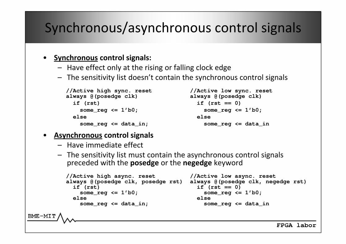
• Synchronous control signals:– Have effect only at the rising or falling clock edge– The sensitivity list doesn’t contain the synchronous control signals
//Active high sync. reset //Active low sync. resetalways @(posedge clk) always @(posedge clk)
if (rst) if (rst == 0)some_reg <= 1’b0; some_reg <= 1’b0;
else elsesome_reg <= data_in; some_reg <= data_in
• Asynchronous control signals– Have immediate effect– The sensitivity list must contain the asynchronous control signals
preceded with the posedge or the negedge keyword//Active high async. reset //Active low async. resetalways @(posedge clk, posedge rst) always @(posedge clk, negedge rst)
if (rst) if (rst == 0)some_reg <= 1’b0; some_reg <= 1’b0;
else elsesome_reg <= data_in; some_reg <= data_in
BME-MITFPGA labor
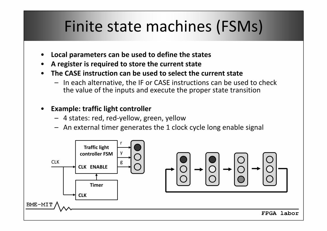
Finite state machines (FSMs)• Local parameters can be used to define the states• A register is required to store the current state• The CASE instruction can be used to select the current state
– In each alternative, the IF or CASE instructions can be used to check the value of the inputs and execute the proper state transition
• Example: traffic light controller– 4 states: red, red‐yellow, green, yellow– An external timer generates the 1 clock cycle long enable signal
Traffic light controller FSM
CLK ENABLE
Timer
CLK
CLK
r
y
g
BME-MITFPGA labor
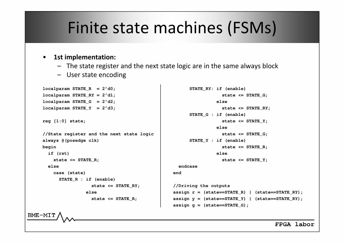
Finite state machines (FSMs)• 1st implementation:
– The state register and the next state logic are in the same always block– User state encoding
localparam STATE_R = 2’d0;localparam STATE_RY = 2’d1;localparam STATE_G = 2’d2;localparam STATE_Y = 2’d3;
reg [1:0] state;
//State register and the next state logicalways @(posedge clk)begin
if (rst)state <= STATE_R;
elsecase (state)
STATE_R : if (enable)state <= STATE_RY;
elsestate <= STATE_R;
STATE_RY: if (enable)state <= STATE_G;
elsestate <= STATE_RY;
STATE_G : if (enable)state <= STATE_Y;
elsestate <= STATE_G;
STATE_Y : if (enable)state <= STATE_R;
elsestate <= STATE_Y;
endcaseend
//Driving the outputsassign r = (state==STATE_R) | (state==STATE_RY);assign y = (state==STATE_Y) | (state==STATE_RY);assign g = (state==STATE_G);
BME-MITFPGA labor
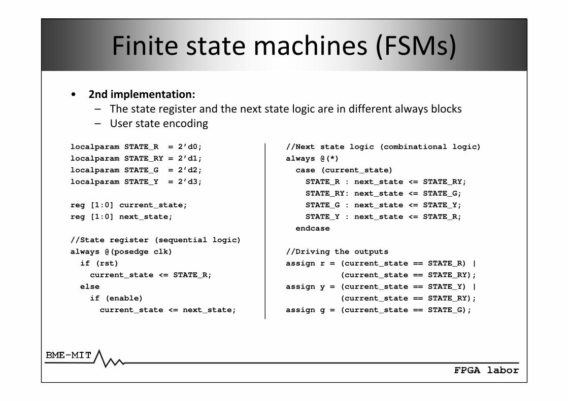
Finite state machines (FSMs)• 2nd implementation:
– The state register and the next state logic are in different always blocks– User state encoding
localparam STATE_R = 2’d0;localparam STATE_RY = 2’d1;localparam STATE_G = 2’d2;localparam STATE_Y = 2’d3;
reg [1:0] current_state;reg [1:0] next_state;
//State register (sequential logic)always @(posedge clk)
if (rst)current_state <= STATE_R;
elseif (enable)
current_state <= next_state;
//Next state logic (combinational logic)always @(*)
case (current_state)STATE_R : next_state <= STATE_RY;STATE_RY: next_state <= STATE_G;STATE_G : next_state <= STATE_Y;STATE_Y : next_state <= STATE_R;
endcase
//Driving the outputsassign r = (current_state == STATE_R) |
(current_state == STATE_RY);assign y = (current_state == STATE_Y) |
(current_state == STATE_RY);assign g = (current_state == STATE_G);
BME-MITFPGA labor
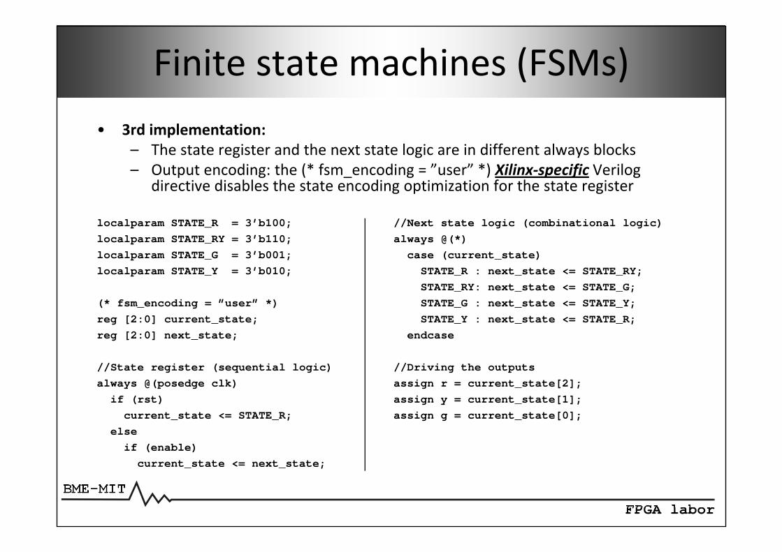
Finite state machines (FSMs)• 3rd implementation:
– The state register and the next state logic are in different always blocks– Output encoding: the (* fsm_encoding = ”user” *) Xilinx‐specific Verilog
directive disables the state encoding optimization for the state register
localparam STATE_R = 3’b100;localparam STATE_RY = 3’b110;localparam STATE_G = 3’b001;localparam STATE_Y = 3’b010;
(* fsm_encoding = ”user” *)reg [2:0] current_state;reg [2:0] next_state;
//State register (sequential logic)always @(posedge clk)
if (rst)current_state <= STATE_R;
elseif (enable)
current_state <= next_state;
//Next state logic (combinational logic)always @(*)
case (current_state)STATE_R : next_state <= STATE_RY;STATE_RY: next_state <= STATE_G;STATE_G : next_state <= STATE_Y;STATE_Y : next_state <= STATE_R;
endcase
//Driving the outputsassign r = current_state[2];assign y = current_state[1];assign g = current_state[0];
BME-MITFPGA labor
Memories (RAMs, ROMs)
• Verilog description of the memories:– Memories can be threated as an one‐dimensional array
• WIDTH: number of bits in a data word• WORDS: number of data words in the memory, this value must be a power of 2
– Memories store data therefore the array must be declared as a register type
reg [WIDTH-1:0] mem [WORDS-1:0];
• Xilinx FPGAs contain two different memory resources– Distributed RAM– Block RAM
BME-MITFPGA labor
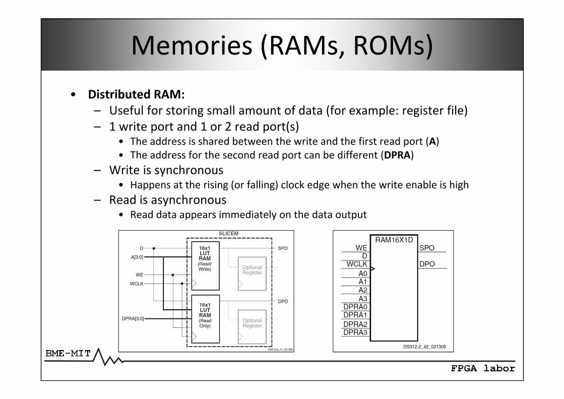
Memories (RAMs, ROMs)• Distributed RAM:
– Useful for storing small amount of data (for example: register file)– 1 write port and 1 or 2 read port(s)
• The address is shared between the write and the first read port (A)• The address for the second read port can be different (DPRA)
– Write is synchronous• Happens at the rising (or falling) clock edge when the write enable is high
– Read is asynchronous• Read data appears immediately on the data output
BME-MITFPGA labor
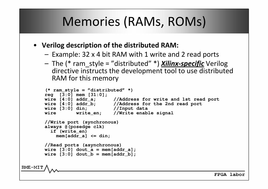
Memories (RAMs, ROMs)• Verilog description of the distributed RAM:
– Example: 32 x 4 bit RAM with 1 write and 2 read ports– The (* ram_style = ”distributed” *) Xilinx‐specific Verilog directive instructs the development tool to use distributed RAM for this memory
(* ram_style = ”distributed” *)reg [3:0] mem [31:0];wire [4:0] addr_a; //Address for write and 1st read portwire [4:0] addr_b; //Address for the 2nd read portwire [3:0] din; //Input datawire write_en; //Write enable signal
//Write port (synchronous)always @(posedge clk)if (write_en)mem[addr_a] <= din;
//Read ports (asynchronous)wire [3:0] dout_a = mem[addr_a];wire [3:0] dout_b = mem[addr_b];
BME-MITFPGA labor
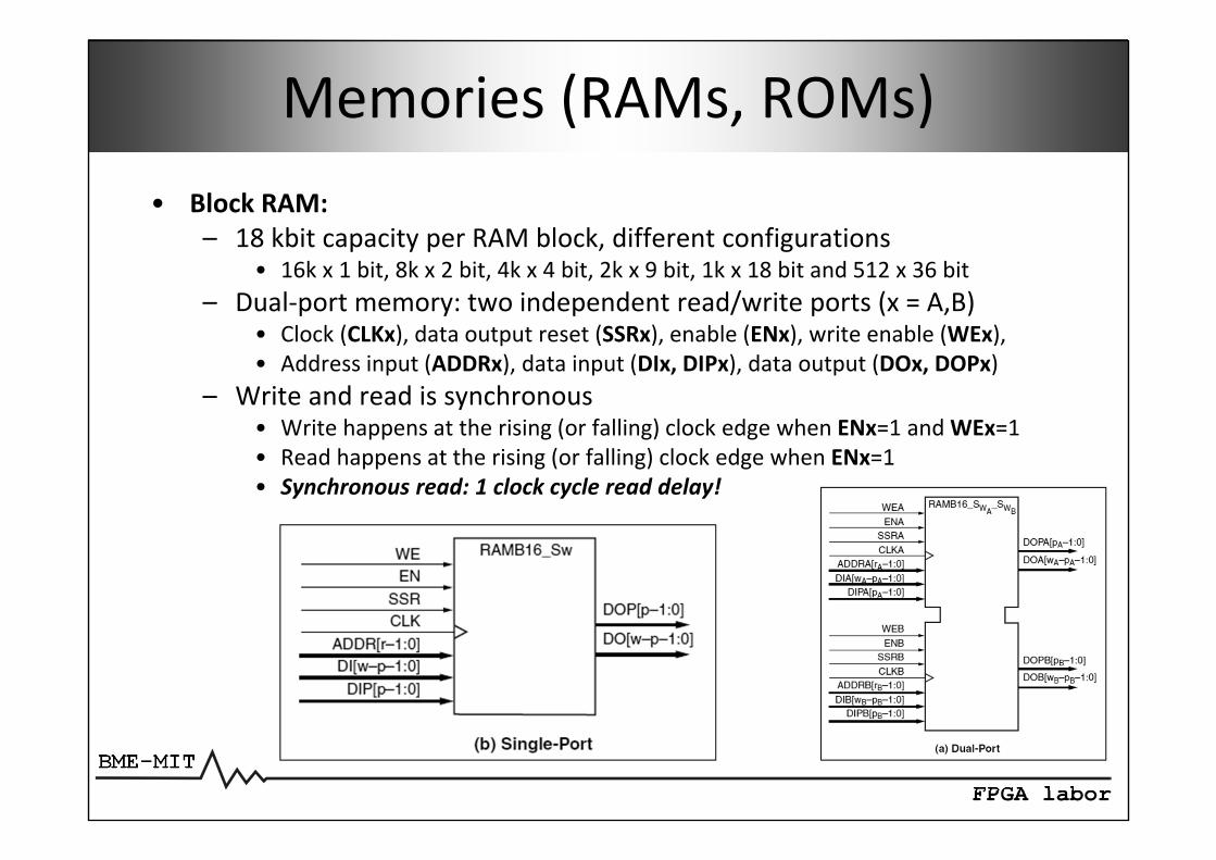
Memories (RAMs, ROMs)• Block RAM:
– 18 kbit capacity per RAM block, different configurations• 16k x 1 bit, 8k x 2 bit, 4k x 4 bit, 2k x 9 bit, 1k x 18 bit and 512 x 36 bit
– Dual‐port memory: two independent read/write ports (x = A,B)• Clock (CLKx), data output reset (SSRx), enable (ENx), write enable (WEx),• Address input (ADDRx), data input (DIx, DIPx), data output (DOx, DOPx)
– Write and read is synchronous• Write happens at the rising (or falling) clock edge when ENx=1 and WEx=1 • Read happens at the rising (or falling) clock edge when ENx=1• Synchronous read: 1 clock cycle read delay!
BME-MITFPGA labor
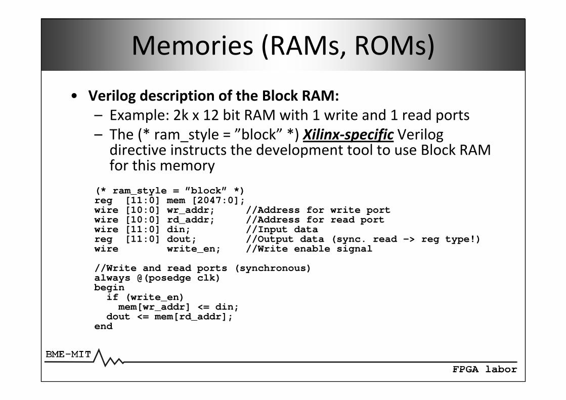
Memories (RAMs, ROMs)• Verilog description of the Block RAM:
– Example: 2k x 12 bit RAM with 1 write and 1 read ports– The (* ram_style = ”block” *) Xilinx‐specific Verilog directive instructs the development tool to use Block RAM for this memory
(* ram_style = ”block” *)reg [11:0] mem [2047:0];wire [10:0] wr_addr; //Address for write portwire [10:0] rd_addr; //Address for read portwire [11:0] din; //Input datareg [11:0] dout; //Output data (sync. read -> reg type!)wire write_en; //Write enable signal
//Write and read ports (synchronous)always @(posedge clk)beginif (write_en)mem[wr_addr] <= din;
dout <= mem[rd_addr];end
BME-MITFPGA labor
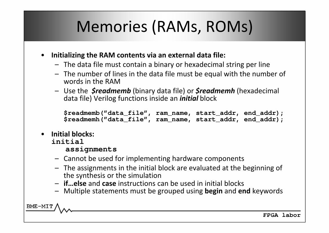
Memories (RAMs, ROMs)• Initializing the RAM contents via an external data file:
– The data file must contain a binary or hexadecimal string per line– The number of lines in the data file must be equal with the number of
words in the RAM– Use the $readmemb (binary data file) or $readmemh (hexadecimal
data file) Verilog functions inside an initial block
$readmemb(”data_file”, ram_name, start_addr, end_addr);$readmemh(”data_file”, ram_name, start_addr, end_addr);
• Initial blocks:initial
assignments– Cannot be used for implementing hardware components– The assignments in the initial block are evaluated at the beginning of
the synthesis or the simulation– if…else and case instructions can be used in initial blocks– Multiple statements must be grouped using begin and end keywords
BME-MITFPGA labor
Memories (RAMs, ROMs)
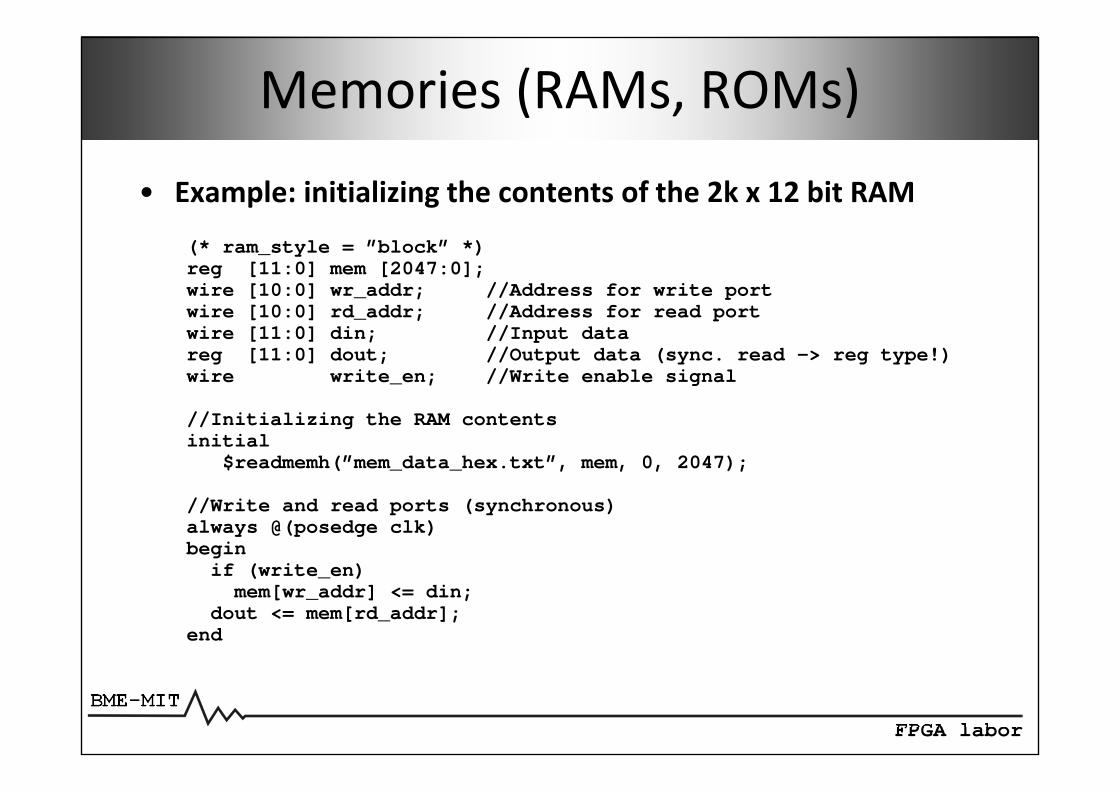
• Example: initializing the contents of the 2k x 12 bit RAM
(* ram_style = ”block” *)reg [11:0] mem [2047:0];wire [10:0] wr_addr; //Address for write portwire [10:0] rd_addr; //Address for read portwire [11:0] din; //Input datareg [11:0] dout; //Output data (sync. read -> reg type!)wire write_en; //Write enable signal
//Initializing the RAM contentsinitial
$readmemh(”mem_data_hex.txt”, mem, 0, 2047);
//Write and read ports (synchronous)always @(posedge clk)beginif (write_en)mem[wr_addr] <= din;
dout <= mem[rd_addr];end
BME-MITFPGA labor
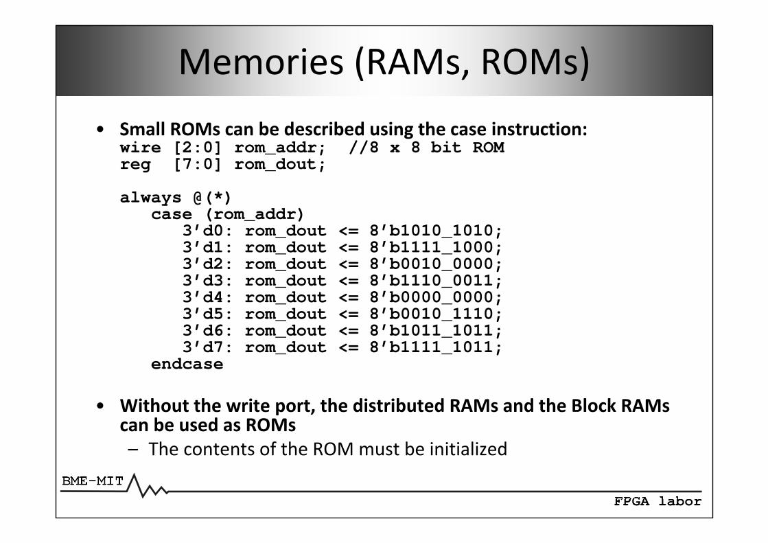
Memories (RAMs, ROMs)• Small ROMs can be described using the case instruction:
wire [2:0] rom_addr; //8 x 8 bit ROMreg [7:0] rom_dout;
always @(*)case (rom_addr)
3’d0: rom_dout <= 8’b1010_1010;3’d1: rom_dout <= 8’b1111_1000;3’d2: rom_dout <= 8’b0010_0000;3’d3: rom_dout <= 8’b1110_0011;3’d4: rom_dout <= 8’b0000_0000;3’d5: rom_dout <= 8’b0010_1110;3’d6: rom_dout <= 8’b1011_1011;3’d7: rom_dout <= 8’b1111_1011;
endcase
• Without the write port, the distributed RAMs and the Block RAMscan be used as ROMs– The contents of the ROM must be initialized

BME-MITFPGA labor
Memories (RAMs, ROMs)
• Verilog description of the distributed ROM:– Example: 32 x 4 bit ROM– The (* rom_style = ”distributed” *) Xilinx‐specific Verilog directive instructs the development tool to use distributed ROM for this memory
(* rom_style = ”distributed” *)reg [3:0] mem [31:0];wire [4:0] rd_addr; //Read addresswire [3:0] dout //Output data
//Initializing the ROM contentsinitial$readmemh(”rom_data_hex.txt”, mem, 0, 31);
//Read port (asynchronous)wire [3:0] dout = mem[rd_addr];
BME-MITFPGA labor
Memories (RAMs, ROMs)• Verilog description of the Block ROM:
– Example: 2k x 12 bit ROM with 2 read ports– The (* rom_style = ”block” *) Xilinx‐specific Verilog directive
instructs the development tool to use Block RAM for this ROM(* rom_style = ”block” *)reg [11:0] mem [2047:0];wire [10:0] rd_addr1; //Address for the first read portwire [10:0] rd_addr2; //Address for the second read portreg [11:0] dout1; //Output data (sync. read -> reg type!)reg [11:0] dout2; //Output data (sync. read -> reg type!)
//Initializing the ROM contentsinitial$readmemh(”rom_data_hex.txt”, mem, 0, 2047);
//Read ports (synchronous)always @(posedge clk)begindout1 <= mem[rd_addr1];dout2 <= mem[rd_addr2];
end
BME-MITFPGA labor
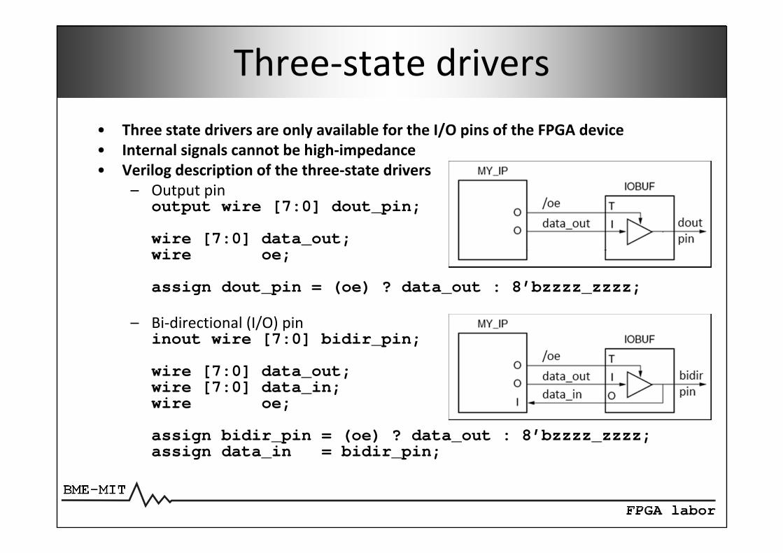
Three‐state drivers• Three state drivers are only available for the I/O pins of the FPGA device• Internal signals cannot be high‐impedance• Verilog description of the three‐state drivers
– Output pinoutput wire [7:0] dout_pin;
wire [7:0] data_out;wire oe;
assign dout_pin = (oe) ? data_out : 8’bzzzz_zzzz;
– Bi‐directional (I/O) pininout wire [7:0] bidir_pin;
wire [7:0] data_out;wire [7:0] data_in;wire oe;
assign bidir_pin = (oe) ? data_out : 8’bzzzz_zzzz;assign data_in = bidir_pin;