Embed Size (px)
Citation preview

Broadband 10Gb/s Graphene Electro-Absorption Modulator on Silicon for Chip-Level Optical Interconnects
Y. T. Hu*, M. Pantouvaki#, S. Brems#, I. Asselberghs#, C. Huyghebaert#, M. Geisler*, C. Alessandri#,
R. Baets*, P. Absil#, D. Van Thourhout* and J. Van Campenhout#
#IMEC, Kapeldreef 75, 3001 Leuven, Belgium
*Ghent University – IMEC, Photonics Research Group, Gent, Belgium Tel: (32) 1628 7732, Email: [email protected]
Abstract We report the first silicon integrated graphene optical electro-absorption modulator capable of 10Gb/s modulation speed. We demonstrate low insertion loss and low drive voltage combined with broadband and athermal operation in a compact hybrid graphene-Si device, outperforming Si(Ge) optical modulators for future chip-level optical interconnect application.
Introduction
Integrated optical modulators with high modulation speed, small footprint and broadband, athermal operation are highly desired to realize high-density low-power optical interconnects tightly integrated with high-performance logic [1-2]. Silicon optical modulators have been strongly optimized over the past few years, but still suffer from large footprint [3], a narrow optical bandwidth or poor temperature tolerance [4]. Alternatively, compact broadband SiGe electro-absorption modulators (EAM) have been demonstrated, but with limited thermal stability [5]. Graphene, which exhibits 2.3% absorption over a wide spectral range from the visible to the infrared owing to its unique linear and gapless band dispersion, is a promising material for robust electro-absorption modulators [6-7]. In this paper, we demonstrate a broadband, athermal and compact graphene-Si EAM operating at 10Gb/s, challenging Si(Ge) modulators for thermally volatile and area sensitive applications such as chip-level optical interconnects.
Device Design and Fabrication
The graphene EAM consists of a graphene-oxide-silicon (GOS) capacitor structure implemented on top of a planarized silicon-on-insulator (SOI) rib waveguide, as shown in Fig. 1. The graphene sheet interacts strongly with the guided optical modes of the sub-micron Si waveguide, and the optical loss can be modulated by controlling the Fermi level in the graphene layer through metal contacts placed on the graphene and Si layer. A modified 130nm CMOS shallow-trench isolation (STI) module with two Si patterning steps was used to define the Si rib waveguides on 200mm SOI wafers. After planarization, three phosphorous ion implantation steps were carried out locally in the Si layer to reduce device resistance. Next, a 5nm thick gate oxide was thermally grown on top of the Si waveguide and the wafer was diced. Subsequently, a single-layer graphene sheet
grown by chemical vapor deposition (CVD) on a Si/SiO2/Cu substrate was transferred to the Si chips using an elastomer stamp [8]. The graphene was patterned by photolithography followed by an oxygen plasma etch. Two separate steps defined the graphene-metal contact (10nm Cr/50nm Au/20nm Ti/420nm Au) and the Si-metal contact (20nm Ti/480nm Au). SEM images of a fabricated device are shown in Fig. 1. Raman data (Fig. 2) indicates that the single layer graphene quality is preserved after processing. Grating couplers [9] were implemented for fiber-to-chip optical coupling.
Fig. 1. Schematic cross section of the hybrid single-layer graphene-Si EAM showing the key structural parameters (a). Simulated optical mode profiles for hybrid graphene-Si waveguides designed for quasi TE (W = 500nm) (b) and TM (W = 750nm) polarized guided modes (c). Optical microscope image showing the graphene EAM test site (d), and top-view (e) and tilted-view (f) SEM images of fabricated devices.

1200 1600 2000 2400 2800 3200
0
200
400
600
800
1000
1200
Raman Shift [cm -1]
Inte
nsity
[a.u
.]
After graphene transferAfter full device processing
2D
G
Fig. 2. Raman spectra of the single-layer graphene sheet after transfer onto the SOI chip and after full device processing. The intensity ratios of the D and G peak (ID/IG~0.3), as well as the 2D and G peak (I2D/IG~1.4) indicate that the graphene quality is maintained after processing.
1520 1540 1560 1580 1600-60
-50
-40
-30
-20
-10
Wavelength [nm]
Rel
ativ
e Tr
ansm
issi
on [d
B]
1520 1560 16000
0.02
0.04
0.06
0.08
Abso
rptio
n [d
B/μm
]
0μm50μm100μm150μm
TE W=500nm
1520 1540 1560 1580 1600-60
-50
-40
-30
-20
-10
Wavelength [nm]
Rel
ativ
e Tr
ansm
issi
on [d
B]
1520 1560 16000
0.05
0.1
0.15
Abso
rptio
n [d
B/μm
]
0μm50μm100μm150μm
TM W=750nm
Fig. 3. Fiber-to-fiber transmission spectra for unbiased TE and TM graphene EAMs with graphene lengths of 50μm, 100μm, 150μm, as well as for reference waveguides without graphene. Graphene-induced waveguide losses are extracted to be 0.06dB/μm for the TE mode and 0.11dB/μm for the TM mode across the full wavelength range (insets). The Gaussian-like roll–off of the transmission at short and long wavelengths originates from the grating coupler pair used for fiber-chip coupling [9].
Static Performance
Transmission spectra of unbiased graphene EAM devices with lengths of 50μm, 100μm, 150μm and reference waveguides without graphene are plotted in Fig. 3, for quasi-transverse electric (TE) and quasi-transverse magnetic (TM) guided modes. Graphene-induced optical absorption losses of ~0.06dB/μm and ~0.11dB/μm are extracted for the TE and TM modes respectively over a wavelength range of 80nm (limited by the grating couplers) around 1560nm (Fig. 3). By
applying drive voltages VD in the range -3V to 3V, an extinction ratio (ER) of ~5dB and on-state insertion loss (IL) below 4dB are obtained for a 50μm TM graphene EAM across the entire wavelength range (Fig. 4), owing to the strong interaction of the TM mode with the graphene sheet (Fig 1). Longer devices enable higher ER, exceeding 10dB for a 150μm device (Fig. 5), at the expense of higher IL. All tested graphene EAM devices exhibited strongest extinction at reverse drive voltages, likely caused by a Fermi-level shift in the graphene sheet due to doping. No significant changes in device response were observed for temperatures in the range 20°C to 49°C, implying robust athermal operation (Fig. 6). Fig. 7 shows the C-V and I-V curves of the graphene EAMs, illustrating GOS accumulation and depletion capacitance for the 50μm long device of ~220fF and ~100fF at VD=2V and -2V respectively, and leakage currents in the nA range.
1520 1540 1560 1580 1600-40
-30
-20
-10
Wavelength [nm]
Rel
ativ
e T
rans
mis
sion
[dB
]
-3V-2V-1V0V1V2V3V
1520 1560 16000
2
4
6
ER
[dB
]
TM W=750nm
-3V~3V
-2V~2V
-1V~1V
Ref. WG
Fig. 4. Fiber-to-fiber transmission spectra of a 50μm TM graphene EAM at different drive voltages. An extinction ratio of ~5dB and insertion loss below 4dB is obtained across the full wavelength range for -3V to 3V voltage swing.
-4 -2 0 2 4-30
-25
-20
-15
-10
-5
0
Voltage [V]
Nor
mal
ized
Tra
nsm
issi
on [d
B]
L=50μmL=100μmL=150μm
λ=1580nm
5.2dB
7.4dB
10.6dB
Normalized to grating couplers Insertion loss:3.76dB
Fig. 5. Static switching curves versus applied voltage of TM graphene modulators with lengths of 50μm, 100μm and 150μm at 1585nm wavelength, normalized for the optical insertion loss of the grating couplers. All EAM devices exhibit maximum absorption at -4V, suggesting a graphene Fermi level close to the Dirac point, and strong absorption bleaching at 4V, suggesting strong hole accumulation (EF < -hν/2, h = Planck’s constant, ν = photon frequency).
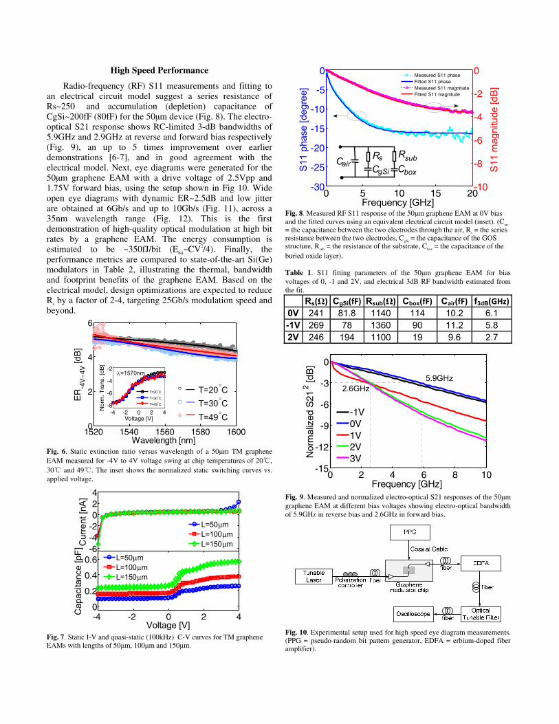
High Speed Performance
Radio-frequency (RF) S11 measurements and fitting to an electrical circuit model suggest a series resistance of Rs~250 and accumulation (depletion) capacitance of CgSi~200fF (80fF) for the 50μm device (Fig. 8). The electro-optical S21 response shows RC-limited 3-dB bandwidths of 5.9GHz and 2.9GHz at reverse and forward bias respectively (Fig. 9), an up to 5 times improvement over earlier demonstrations [6-7], and in good agreement with the electrical model. Next, eye diagrams were generated for the 50μm graphene EAM with a drive voltage of 2.5Vpp and 1.75V forward bias, using the setup shown in Fig 10. Wide open eye diagrams with dynamic ER~2.5dB and low jitter are obtained at 6Gb/s and up to 10Gb/s (Fig. 11), across a 35nm wavelength range (Fig. 12). This is the first demonstration of high-quality optical modulation at high bit rates by a graphene EAM. The energy consumption is estimated to be ~350fJ/bit (Ebit~CV2/4). Finally, the performance metrics are compared to state-of-the-art Si(Ge) modulators in Table 2, illustrating the thermal, bandwidth and footprint benefits of the graphene EAM. Based on the electrical model, design optimizations are expected to reduce Rs by a factor of 2-4, targeting 25Gb/s modulation speed and beyond.
1520 1540 1560 1580 16000
2
4
6
Wavelength [nm]
ER
-4V
~4V
[dB
]
-4 -2 0 2 4-8
-6
-4
-2
Voltage [V]
Nor
m. T
rans
. [d
B]
T=20°C
T=30°C
T=49°C
T=20°C T=30°C T=49°C
λ=1570nm
———
Fig. 6. Static extinction ratio versus wavelength of a 50μm TM graphene EAM measured for -4V to 4V voltage swing at chip temperatures of 20, 30 and 49. The inset shows the normalized static switching curves vs. applied voltage.
-6-4-2024
Voltage (V)
Cur
rent
[nA
]
-4 -2 0 2 40
0.2
0.4
0.6
Voltage [V]
Cap
acita
nce
[pF]
L=50μmL=100μmL=150μm
L=50μmL=100μmL=150μm
Fig. 7. Static I-V and quasi-static (100kHz) C-V curves for TM graphene EAMs with lengths of 50μm, 100μm and 150μm.
0 5 10 15 20-30
-25
-20
-15
-10
-5
0
Frequency [GHz]
S11
phas
e [d
egre
e]
-10
-8
-6
-4
-2
0
S11
mag
nitu
de [d
B]
Measured S11 phaseFitted S11 phaseMeasured S11 magnitudeFitted S11 magnitude
s
box
subRRgSi
Cair C C
Fig. 8. Measured RF S11 response of the 50μm graphene EAM at 0V bias and the fitted curves using an equivalent electrical circuit model (inset). (Cair = the capacitance between the two electrodes through the air, Rs = the series resistance between the two electrodes, CgSi = the capacitance of the GOS structure, Rsub = the resistance of the substrate, Cbox = the capacitance of the buried oxide layer).
Table 1. S11 fitting parameters of the 50μm graphene EAM for bias voltages of 0, -1 and 2V, and electrical 3dB RF bandwidth estimated from the fit.
Rs(Ω) CgSi(fF) Rsub(Ω) Cbox(fF) Cair(fF) f3dB(GHz)0V 241 81.8 1140 114 10.2 6.1 -1V 269 78 1360 90 11.2 5.8 2V 246 194 1100 19 9.6 2.7
0 2 4 6 8 10-15
-12
-9
-6
-3
0
Frequency [GHz]
Nor
mal
ized
S21
2 [dB
]
-1V0V1V2V3V
5.9GHz2.6GHz
Fig. 9. Measured and normalized electro-optical S21 responses of the 50μm graphene EAM at different bias voltages showing electro-optical bandwidth of 5.9GHz in reverse bias and 2.6GHz in forward bias.
Fig. 10. Experimental setup used for high speed eye diagram measurements. (PPG = pseudo-random bit pattern generator, EDFA = erbium-doped fiber amplifier).
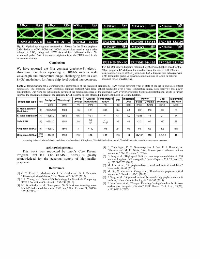
Fig. 11. Optical eye diagrams measured at 1560nm for the 50μm graphene EAM device at 6Gb/s, 8Gb/s and 10Gb/s modulation speed, using a drive voltage of 2.5Vpp swing and 1.75V forward bias delivered with a 50 terminated probe. Part of the noise originates from the EDFA used in the measurement setup.
Conclusion
We have reported the first compact graphene-Si electro-absorption modulator operating at 10Gb/s over a wide wavelength and temperature range, challenging best-in-class Si(Ge) modulators for future chip-level optical interconnects.
Fig. 12. Optical eye diagrams measured at 10Gb/s modulation speed for the 50μm graphene EAM device for wavelengths in the range 1530-1565nm, using a drive voltage of 2.5Vpp swing and 1.75V forward bias delivered with a 50 terminated probe. A dynamic extinction ratio of 2.3dB or better is obtained for all wavelengths.
Table 2. Benchmarking table comparing the performance of the presented graphene-Si EAM versus different types of state-of-the-art Si and SiGe optical modulators. The graphene EAM combines compact footprint with large optical bandwidth over a wide temperature range, with relatively low power consumption. Our work has substantially advanced the modulation speed of the graphene EAM over prior reports. Significant potential still exists to further improve the modulation speed of the graphene EAM closer to speeds obtained in highly optimized Si(Ge) modulators.
Modulator type Ref. Footprint Wavelength Drive voltage
Optical bandwidth
Temperature range ER Insertion
Loss Power 3dB
frequencyMaximum Bit Rate Static Dynamic
[μm2] [nm] [V] [nm] [] [dB] [dB] [mW] [fJ/bit] [GHz] [Gb/s]
Si Mach-Zehnder Modulator [3] ~3000x500 1300 1.5 >80* >80* 3.4 7.1 ~20# 450 30 50
Si Ring Modulator [4] ~10x10 1550 0.5 <0.1 <1 6.4 1.2 <0.01 ~1 21 44
SiGe EAM [5] ~55x10 1550 2.8 35 5§
<1 <40§ ~5 ~4 >2.2 60 >30 28
Graphene-Si EAM [6] ~40x10 1500 3 >180 n/a 2.4 n/a n/a n/a 1.2 n/a
Graphene-Si EAM This work ~50x10 1550 2.5 >80 >29 2.5 <4 <1x10⁻⁴ 350 2.6-5.9 10
*Assuming balanced Mach-Zehnder modulator with broadband 3dB splitters, #Mach-Zehnder bias control, §Bandwidth can be traded for temperature tolerance.
Acknowledgements
This work was supported by imec’s Core Partner Program. Prof B.J. Cho (KAIST, Korea) is greatly acknowledged for the generous supply of high-quality graphene.
References
[1]. G. T. Reed, G. Mashanovich, F. Y. Gardes and D. J. Thomson, “Silicon optical modulators,” Nat. Photon. 4, 518–526 (2010).
[2]. I. A. Young, et al. Optical I/O Technology for Tera-Scale Computing. IEEE J. Solid-State Circuits 45.1, 235–248 (2010).
[3]. M. Streshinsky, et al, “Low power 50 Gb/s silicon traveling wave Mach-Zehnder modulator near 1300 nm,” Opt. Express 21, 30350-30357 (2013).
[4]. E. Timurdogan, C. M. Sorace-Agaskar, J. Sun, E. S. Hosseini, A. Biberman and M. R. Watts, “An ultralow power athermal silicon modulator,” Nat. Commun. 5, (2014).
[5]. D. Feng, et al., “High speed GeSi electro-absorption modulator at 1550 nm wavelength on SOI waveguide,” Optics Express, Vol. 20, Issue 20, pp. 22224-22232 (2012).
[6]. M. Liu, et al., “A graphene-based broadband optical modulator,” Nature 474, 64–67 (2011).
[7]. M. Liu, X. Yin and X. Zhang et al., “Double-layer graphene optical modulator,” Nano Lett. 12(3) (2012).
[8]. J. Song, et al., “A general method for transferring graphene onto soft surfaces,” Nature Nanotechnology 8, 356–362 (2013).
[9]. F. Van Laere, et al., “Compact Focusing Grating Couplers for Silicon-on-Insulator Integrated Circuits,” IEEE Photon. Tech. Lett., 19(23), p.1919-1921 (2007).


![High-Speed Plasmonic-Silicon Modulator Driven by Epsilon ...graphene [5], [6], electro-optic polymer[7], [8], and phase change materials [9]. Such hybrid plasmonic-silicon photonic](https://img.pdfslide.net/doc/110x75/60bafd81731e884d3b7afae2/high-speed-plasmonic-silicon-modulator-driven-by-epsilon-graphene-5-6.jpg)