Embed Size (px)
Citation preview
Broadband absorption enhancement achieved by optical layer mediated plasmonic solar cell
Wenzhen Ren, Guanghui Zhang, Yukun Wu, Huaiyi Ding, Qinghe Shen, Kun Zhang, Junwen Li, Nan Pan,
* and Xiaoping Wang
Hefei National Laboratory for Physical Sciences at the Microscale and Department of Physics, University of Science and Technology of China, Hefei 230026, China
Abstract: We propose a novel thin solar cell design, integrating plasmonic component with optical layer, for conspicuous performance improvement in organic (P3HT: PCBM) thin film solar cell. Despite the relatively simple structure, the designed solar cell can get strikingly high spectral performance with the short circuit current density (Jsc) enhancement up to 67%; and a nicely large Jsc enhancement over 50% can be easily obtained spanning rather a broad geometric parametric range. The mechanisms responsible for this significant and broadband absorption enhancement as well as the effects of intercalating a plasmonic nanoparticles (NPs) array and an optical layer are theoretically and systematically investigated by finite-difference time-domain calculations (FDTD). The origin of the dramatically increased absorption is believed to be the synergistic effect between 1) the enhanced electric field and forward scattering upon excitation of localized surface plasmon resonance (LSPR) of the NPs, and 2) the favorable redistributions of light field in the device due to the beneficial interference effect mediated by the optical layer. Such a design concept is quite versatile and can be easily extended to other thin film solar cell systems.
©2011 Optical Society of America
OCIS codes: (350.6050) Solar energy; (250.5403) Plasmonics; (040.5350) Photovoltaic; (240.6680) Surface plasmons; (310.6845) Thin film devices and applications.
References and links
1. R. Kroon, M. Lenes, J. C. Hummelen, P. W. M. Blom, and B. De Boer, “Small bandgap polymers for organic solar cells,” Pol. Rev. 48(3), 531–582 (2008).
2. S. I. Na, B. K. Yu, S. S. Kim, D. Vak, T. S. Kim, J. S. Yeo, and D. Y. Kim, “Fully spray-coated ITO-free organic solar cells for low-cost power generation,” Sol. Energy Mater. Sol. Cells 94(8), 1333–1337 (2010).
3. P. Peumans, A. Yakimov, and S. R. Forrest, “Small molecular weight organic thin-film photodetectors and solar cells,” J. Appl. Phys. 93(7), 3693–3723 (2003).
4. V. E. Ferry, J. N. Munday, and H. A. Atwater, “Design considerations for plasmonic photovoltaics,” Adv. Mater. (Deerfield Beach Fla.) 22(43), 4794–4808 (2010).
5. V. E. Ferry, L. A. Sweatlock, D. Pacifici, and H. A. Atwater, “Plasmonic nanostructure design for efficient light coupling into solar cells,” Nano Lett. 8(12), 4391–4397 (2008).
6. B. P. Rand, P. Peumans, and S. R. Forrest, “Long-range absorption enhancement in organic tandem thin-film solar cells containing silver nanoclusters,” J. Appl. Phys. 96(12), 7519–7526 (2004).
7. C. J. Min, J. Li, G. Veronis, J. Y. Lee, S. H. Fan, and P. Peumans, “Enhancement of optical absorption in thin-film organic solar cells through the excitation of plasmonic modes in metallic gratings,” Appl. Phys. Lett. 96(13), 133302 (2010).
#154449 - $15.00 USD Received 9 Sep 2011; revised 21 Nov 2011; accepted 28 Nov 2011; published 13 Dec 2011(C) 2011 OSA 19 December 2011 / Vol. 19, No. 27 / OPTICS EXPRESS 26536

8. J. N. Munday and H. A. Atwater, “Large integrated absorption enhancement in plasmonic solar cells by combining metallic gratings and antireflection coatings,” Nano Lett. 11(6), 2195–2201 (2011).
9. H. A. Atwater and A. Polman, “Plasmonics for improved photovoltaic devices,” Nat. Mater. 9(3), 205–213 (2010).
10. K. R. Catchpole and A. Polman, “Design principles for particle plasmon enhanced solar cells,” Appl. Phys. Lett. 93(19), 191113 (2008).
11. C. H. Kim, S.-H. Cha, S. C. Kim, M. Song, J. Lee, W. S. Shin, S.-J. Moon, J. H. Bahng, N. A. Kotov, and S.-H. Jin, “Silver nanowire embedded in P3HT:PCBM for high-efficiency hybrid photovoltaic device applications,” ACS Nano 5(4), 3319–3325 (2011).
12. W. L. Bai, Q. Q. Gan, G. F. Song, L. H. Chen, Z. Kafafi, and F. Bartoli, “Broadband short-range surface plasmon structures for absorption enhancement in organic photovoltaics,” Opt. Express 18(S4 Suppl 4), A620–A630 (2010).
13. S. J. Tsai, M. Ballarotto, D. B. Romero, W. N. Herman, H. C. Kan, and R. J. Phaneuf, “Effect of gold nanopillar arrays on the absorption spectrum of a bulk heterojunction organic solar cell,” Opt. Express 18(S4 Suppl 4), A528–A535 (2010).
14. A. J. Morfa, K. L. Rowlen, T. H. Reilly, M. J. Romero, and J. van de Lagemaat, “Plasmon-enhanced solar energy conversion in organic bulk heterojunction photovoltaics,” Appl. Phys. Lett. 92(1), 013504 (2008).
15. S. Pillai, K. R. Catchpole, T. Trupke, and M. A. Green, “Surface plasmon enhanced silicon solar cells,” J. Appl. Phys. 101(9), 093105 (2007).
16. M. A. Sefunc, A. K. Okyay, and H. V. Demir, “Volumetric plasmonic resonator architecture for thin-film solar cells,” Appl. Phys. Lett. 98(9), 093117 (2011).
17. L. Qian, J. Yang, R. Zhou, A. Tang, Y. Zheng, T.-K. Tseng, D. Bera, J. Xue, and P. H. Holloway, “Hybrid polymer-CdSe solar cells with a ZnO nanoparticle buffer layer for improved efficiency and lifetime,” J. Mater. Chem. 21(11), 3814–3817 (2011).
18. J. Y. Kim, S. H. Kim, H. H. Lee, K. Lee, W. L. Ma, X. Gong, and A. J. Heeger, “New architecture for high-efficiency polymer photovoltaic cells using solution-based titanium oxide as an optical spacer,” Adv. Mater. (Deerfield Beach Fla.) 18(5), 572–576 (2006).
19. F.-C. Chen, J.-L. Wu, and Y. Hung, “Spatial redistribution of the optical field intensity in inverted polymer solar cells,” Appl. Phys. Lett. 96(19), 193304 (2010).
20. J. Gilot, I. Barbu, M. M. Wienk, and R. A. J. Janssen, “The use of ZnO as optical spacer in polymer solar cells: theoretical and experimental study,” Appl. Phys. Lett. 91(11), 113520 (2007).
21. E. D. Palik, ed., Handbook of Optical Constants of Solids (Academic, New York, 1985). 22. H. H. Shen, P. Bienstman, and B. Maes, “Plasmonic absorption enhancement in organic solar cells with thin
active layers,” J. Appl. Phys. 106(7), 073109 (2009). 23. Q. L. Gu, “Plasmonic metallic nanostructures for efficient absorption enhancement in ultrathin CdTe-based
photovoltaic cells,” J. Phys. D Appl. Phys. 43(46), 465101 (2010). 24. S. A. Maier, Plasmonics: Fundamentals and Applications (Springer, New York, 2007). 25. K. A. Willets and R. P. Van Duyne, “Localized surface plasmon resonance spectroscopy and sensing,” Annu.
Rev. Phys. Chem. 58(1), 267–297 (2007). 26. J. Zhao, A. O. Pinchuk, J. M. McMahon, S. Li, L. K. Ausman, A. L. Atkinson, and G. C. Schatz, “Methods for
describing the electromagnetic properties of silver and gold nanoparticles,” Acc. Chem. Res. 41(12), 1710–1720 (2008).
27. Y. A. Akimov, W. S. Koh, and K. Ostrikov, “Enhancement of optical absorption in thin-film solar cells through the excitation of higher-order nanoparticle plasmon modes,” Opt. Express 17(12), 10195–10205 (2009).
28. B. J. Wiley, S. H. Im, Z. Y. Li, J. McLellan, A. Siekkinen, and Y. A. Xia, “Maneuvering the surface plasmon resonance of silver nanostructures through shape-controlled synthesis,” J. Phys. Chem. B 110(32), 15666–15675 (2006).
29. E. Prodan, C. Radloff, N. J. Halas, and P. Nordlander, “A hybridization model for the plasmon response of complex nanostructures,” Science 302(5644), 419–422 (2003).
30. B. Auguié and W. L. Barnes, “Collective resonances in gold nanoparticle arrays,” Phys. Rev. Lett. 101(14), 143902 (2008).
31. T. A. M. Ferenczi, J. Nelson, C. Belton, A. M. Ballantyne, M. Campoy-Quiles, F. M. Braun, and D. D. C. Bradley, “Planar heterojunction organic photovoltaic diodes via a novel stamp transfer process,” J. Phys. Condens. Matter 20(47), 475203 (2008).
Introduction
To help relieve fossil energy shortage in near future as well as environmental concerns escalating with increasing energy consumption and exhaust emissions, efficient exploitation of clean, safe and renewable energies such as solar energy have been greatly pursued. Among these endeavors, considerable efforts have been made to design new organic thin film photovoltaics (PVs) and optimize the performance of them [1–3] because of their potentials for large-scale and low-cost solar energy conversion. Due to the inherent incomplete absorption in thin film solar cells, effective light trapping without degrading the carrier collection efficiency is exceptionally important. On one hand, it has been demonstrated recently that the use of metallic nanostructures in solar cells could result in large optical field
#154449 - $15.00 USD Received 9 Sep 2011; revised 21 Nov 2011; accepted 28 Nov 2011; published 13 Dec 2011(C) 2011 OSA 19 December 2011 / Vol. 19, No. 27 / OPTICS EXPRESS 26537
enhancement and absorption improvement [4–9]. When incident light encounters a scattering structure, it will be preferentially scattered into the medium with higher optical density; this favorable forward scattering can be employed to couple incident light into underlying layers of active materials to increase the absorption [10]. In fact, an incorporation of plasmonic scattering structures with conventional PVs has been shown to enable photocurrent to increase effectively and may lead to new opportunities for inexpensive, high-efficiency solar cell designs [6,11–15]. To meet the goal of even higher cell efficiency, some new plasmonic designs have been proposed very recently, e.g., double- and even multi-layered plasmonic designs with active materials sandwiched/intercalated by two or more layers of plasmonic nano-patterned structures [16]. Although the efficiency could in principle be greatly enhanced, such device architectures are rather complicated and hence not suitable for a practical application. On the other hand, it is also found that the interference between incident and reflected light cannot be neglected in thin solar cells and a proper optical layer can position larger optical field in active layers to increase total absorption [17–20]. Although the absorption enhancements in optical layer mediated thin PVs are usually moderate as compared with those in plasmonic PVs, these structures are extremely easy to fabricate and are perfectly compatible with large-scale and low-cost production techniques. In addition, an optical layer may also improve the exciton diffusion and device stability [17].
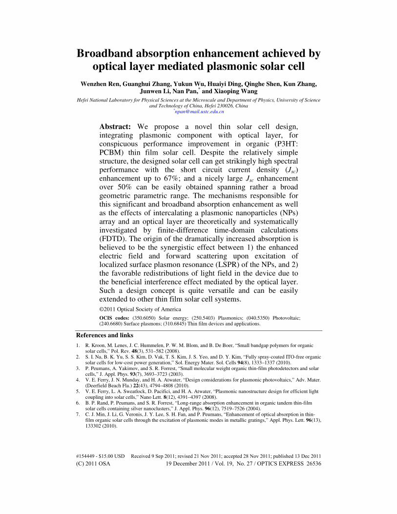
It is very interesting to ask what will happen if an optical layer is integrated with a plasmonic thin solar cell design. In such a device, the internal light field may be drastically modulated under the possible co-effect of plasmonic structures and optical layer, which certainly will affect the overall conversion efficiency, either positively or negatively. Therefore, it is worth understanding how the co-effect works and how it can be beneficially/optimally exploited through this “integrated” design, which could be very important towards more efficient thin film PVs design. More interestingly, the possible “multiple” efficiency gains through simply inserting an optical layer are hardly at any cost of complicated fabrication or sacrificed compatibility. For this reason, we construct a new optical layer mediated plasmonic thin solar cell, as shown in Fig. 1(c), where an Ag nanoparticles (NPs) array is forwardly laid on a transparent electrode (e.g., indium doped tin oxide) and a conductive optical layer is inserted between an active layer and a metal electrode (e.g., Ag).
In this work, we report a striking and broadband absorption enhancement in such a thin solar cell using the blend of poly(3-hexylthiophene) (P3HT) and [6]-phenyl-C61-butyric acid methyl ester (PCBM) as the active layer (which is very commonly used experimentally), through incorporating plasmon-enhanced light trapping, optical layer mediated favorable interference and the synergistic effect therein. First, we state the numerical calculation method for evaluating the device performance. Then we comparatively study the overall performance for optimized devices with only a plasmonic design and a “hybrid” design integrating plasmonics with optical layer. Next, we further investigate the roles of metallic NPs, optical layer and their interaction; we demonstrate that significant and broadband sunlight absorption enhancements can be achieved in these proposed devices within rather a broad designed parametric range, suggesting a nicely high degree of technological tolerance and feasibility.
Device architecture and numerical calculation method
A conventional device structure of the organic bulk heterojunction thin film solar cells, serving as the reference, is given in Fig. 1(a). In the reference cell, the bottom electrode is a 100 nm Ag layer, atop of which is an active layer of a 40 nm P3HT:PCBM blend film; a 20 nm PEDOT:PSS film as the hole transporting layer and a 50 nm indium doped tin oxide (ITO) film as the transparent forward electrode are sequentially spun. As for the proposed solar cell architectures, the one with only plasmonic component is shown in Fig. 1(b), where a square array of Ag metal NPs with designable radius (r) and period (P) is introduced as light trapping antennas on the top of ITO, leaving all other structures the same as the reference cell. In order to further modulate the overall performance both plasmonically and optically, a thin film of a
#154449 - $15.00 USD Received 9 Sep 2011; revised 21 Nov 2011; accepted 28 Nov 2011; published 13 Dec 2011(C) 2011 OSA 19 December 2011 / Vol. 19, No. 27 / OPTICS EXPRESS 26538
conductive dielectric material is inserted between the active layer and the Ag electrode as an optical layer, as shown in Fig. 1(c).
Fig. 1. Schematic diagrams for a reference solar cell (a), a plasmonic solar cell without an optical layer (b), and a plasmonic solar cell integrated with an optical layer design (c).
Finite-difference time-domain (FDTD) algorithm (Lumerical Solutions Inc., Canada) is adopted for rigorous three dimensional (3D) electromagnetic propagation calculations. In the calculations, plane waves are normally incident from the transparent conductive electrode into the cells. Perfectly matched layer (PML) absorbing boundary conditions are used on the upper and lower boundaries in z-direction (as indicated in Fig. 1). The incident light is set polarized along x-axis, and then anti-symmetric boundary conditions for x-axis and symmetric boundary conditions for y-axis are used for reducing the simulation volume. The sunlight, unpolarized, can be treated as the incoherent superposition of two orthogonally- polarized components (e.g., x- and y-polarized), the overall device response (R) is the intensity incoherent superposition of each contribution, i.e., with R = (Rx-polarized + Ry-polarized)/2. Due to the high symmetry of the structure, the polarization does not affect the overall performance; in other words, the obtained photovoltaic response is exactly the same regardless of the incident light is x- or y-polarized, i.e., R = Rx-polarized = Ry-polarized. Therefore, in this case, the simple x-polarized setting of the incident light is enough to reflect the overall response of the device. The FDTD approach also allows us to use the experimental refractive index data to represent the materials’ characteristics including Ag [21], ITO, P3HT:PCBM and PEDOT:PSS [22,23] in our device structures. In all of the simulations, the complex refractive index of ITO has been adopted to include the possible effect of its high free carrier concentration on the plasmon resonance of the adjacent Ag NPs. Before the simulations start, we have carried out a series of convergency tests as well as the careful comparisons with other numerical and analytic methods to ensure the numerical stability and accuracy.
Through computing the distribution of electric field in the device, the absorption per unit volume in an absorptive material [8], Ploss, can be obtained from the following equation:
21
| | Im( ),2
lossP Eω ε= (1)
where |E|2 is the magnitude of the electric field squared within the material, Im(ε) is the
imaginary part of the dielectric function for each layer and ω is the angular frequency of the incident electric field. Integrating the absorption per unit volume (Ploss) over the entire region for each absorptive material, the optical absorption (A) can then be obtained by normalizing the power absorbed by the material to the source power:
( ) ,lossabs
in in
P dVPA
P Pλ = =
∫ (2)
where Pabs is the power absorbed by the absorptive material, Pin is the incident source power. To evaluate the short circuit current density (Jsc), the results are weighted by solar irradiance
#154449 - $15.00 USD Received 9 Sep 2011; revised 21 Nov 2011; accepted 28 Nov 2011; published 13 Dec 2011(C) 2011 OSA 19 December 2011 / Vol. 19, No. 27 / OPTICS EXPRESS 26539
spectrum under the standard air mass, namely AM1.5 solar spectrum. If we assume that all the electron-hole pairs contribute to the photocurrent, the Jsc can be derived as:
1.5
( ) ( ) ,sc ac AM
J e A I dhc
λλ λ λ= ∫ (3)
where h is Plank constant, c is the speed of light in free space, IAM1.5 is the solar irradiance spectrum under the standard air mass and Aac(λ) is the absorption of active layer, i.e., P3HT:PCBM.
In order to further investigate the underlying mechanism for the optical layer mediated field enhancement, the average electric intensity distribution in the device along the z-axis within the desired wavelength range, E(z, λ), is calculated as:
2 2
| ( ; ) | | ( , , ; ) | / ,E z E x y z dxdy dxdyλ λ= ∫∫ ∫∫ (4)
where |E(x, y, z; λ)|2 is the electric field intensity for a spatial position (x, y, z) at a certain
wavelength of λ.
The performance of the optimized solar cells
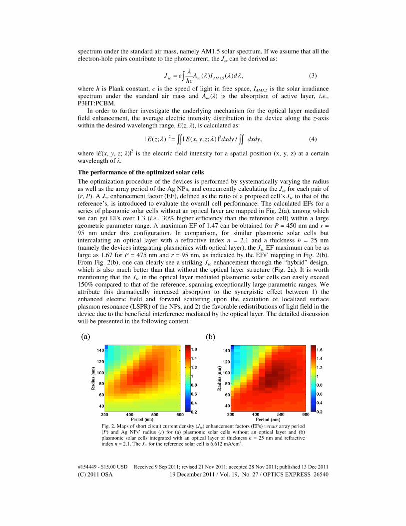
The optimization procedure of the devices is performed by systematically varying the radius as well as the array period of the Ag NPs, and concurrently calculating the Jsc for each pair of (r, P). A Jsc enhancement factor (EF), defined as the ratio of a proposed cell’s Jsc to that of the reference’s, is introduced to evaluate the overall cell performance. The calculated EFs for a series of plasmonic solar cells without an optical layer are mapped in Fig. 2(a), among which we can get EFs over 1.3 (i.e., 30% higher efficiency than the reference cell) within a large geometric parameter range. A maximum EF of 1.47 can be obtained for P = 450 nm and r = 95 nm under this configuration. In comparison, for similar plasmonic solar cells but intercalating an optical layer with a refractive index n = 2.1 and a thickness h = 25 nm (namely the devices integrating plasmonics with optical layer), the Jsc EF maximum can be as large as 1.67 for P = 475 nm and r = 95 nm, as indicated by the EFs’ mapping in Fig. 2(b). From Fig. 2(b), one can clearly see a striking Jsc enhancement through the “hybrid” design, which is also much better than that without the optical layer structure (Fig. 2a). It is worth mentioning that the Jsc in the optical layer mediated plasmonic solar cells can easily exceed 150% compared to that of the reference, spanning exceptionally large parametric ranges. We attribute this dramatically increased absorption to the synergistic effect between 1) the enhanced electric field and forward scattering upon the excitation of localized surface plasmon resonance (LSPR) of the NPs, and 2) the favorable redistributions of light field in the device due to the beneficial interference mediated by the optical layer. The detailed discussion will be presented in the following content.
Fig. 2. Maps of short circuit current density (Jsc) enhancement factors (EFs) versus array period (P) and Ag NPs’ radius (r) for (a) plasmonic solar cells without an optical layer and (b) plasmonic solar cells integrated with an optical layer of thickness h = 25 nm and refractive index n = 2.1. The Jsc for the reference solar cell is 6.612 mA/cm2.
#154449 - $15.00 USD Received 9 Sep 2011; revised 21 Nov 2011; accepted 28 Nov 2011; published 13 Dec 2011(C) 2011 OSA 19 December 2011 / Vol. 19, No. 27 / OPTICS EXPRESS 26540
It is well known that metallic NPs support localized surface plasmons (LSP), i.e., the localized collective oscillations of conduction electrons around the NP’s surface [15,24–26]. When the frequency of incident light closes to the LSPR of a metallic NP, it can strongly couple with the induced surface charges on the NP. In this case, the incident light interacts with the NP over an area much larger than its actual geometric cross-section, leading to extraordinary scattering and absorption which can be tailored to improve the performance of PVs [15,25–27]. The contribution of surface plasmon to light absorption and scattering by metallic NPs depends strongly on size, shape [28] and surrounding dielectric environment [15], and the interaction between the modes of individual NPs can also form new hybrid modes that could also affect the extinction [29,30]
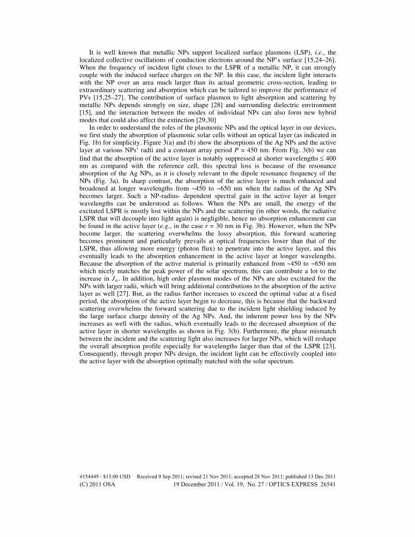
In order to understand the roles of the plasmonic NPs and the optical layer in our devices, we first study the absorption of plasmonic solar cells without an optical layer (as indicated in Fig. 1b) for simplicity. Figure 3(a) and (b) show the absorptions of the Ag NPs and the active layer at various NPs’ radii and a constant array period P = 450 nm. From Fig. 3(b) we can
find that the absorption of the active layer is notably suppressed at shorter wavelengths ≤ 400 nm as compared with the reference cell, this spectral loss is because of the resonance absorption of the Ag NPs, as it is closely relevant to the dipole resonance frequency of the NPs (Fig. 3a). In sharp contrast, the absorption of the active layer is much enhanced and broadened at longer wavelengths from ~450 to ~650 nm when the radius of the Ag NPs becomes larger. Such a NP-radius- dependent spectral gain in the active layer at longer wavelengths can be understood as follows. When the NPs are small, the energy of the excitated LSPR is mostly lost within the NPs and the scattering (in other words, the radiative LSPR that will decouple into light again) is negligible, hence no absorption enhancement can be found in the active layer (e.g., in the case r = 30 nm in Fig. 3b). However, when the NPs become larger, the scattering overwhelms the lossy absorption, this forward scattering becomes prominent and particularly prevails at optical frequencies lower than that of the LSPR, thus allowing more energy (photon flux) to penetrate into the active layer, and this eventually leads to the absorption enhancement in the active layer at longer wavelengths. Because the absorption of the active material is primarily enhanced from ~450 to ~650 nm which nicely matches the peak power of the solar spectrum, this can contribute a lot to the increase in Jsc. In addition, high order plasmon modes of the NPs are also excitated for the NPs with larger radii, which will bring additional contributions to the absorption of the active layer as well [27]. But, as the radius further increases to exceed the optimal value at a fixed period, the absorption of the active layer begin to decrease, this is because that the backward scattering overwhelms the forward scattering due to the incident light shielding induced by the large surface charge density of the Ag NPs. And, the inherent power loss by the NPs increases as well with the radius, which eventually leads to the decreased absorption of the active layer in shorter wavelengths as shown in Fig. 3(b). Furthermore, the phase mismatch between the incident and the scattering light also increases for larger NPs, which will reshape the overall absorption profile especially for wavelengths larger than that of the LSPR [23]. Consequently, through proper NPs design, the incident light can be effectively coupled into the active layer with the absorption optimally matched with the solar spectrum.
#154449 - $15.00 USD Received 9 Sep 2011; revised 21 Nov 2011; accepted 28 Nov 2011; published 13 Dec 2011(C) 2011 OSA 19 December 2011 / Vol. 19, No. 27 / OPTICS EXPRESS 26541
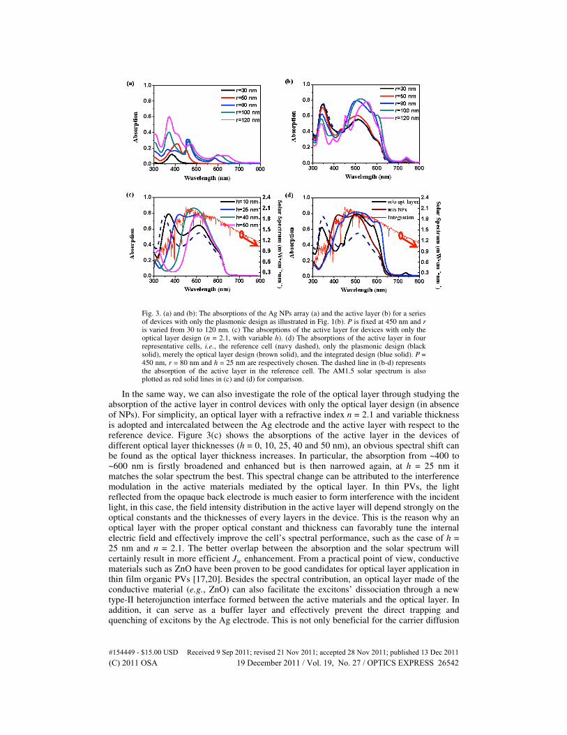
Fig. 3. (a) and (b): The absorptions of the Ag NPs array (a) and the active layer (b) for a series of devices with only the plasmonic design as illustrated in Fig. 1(b). P is fixed at 450 nm and r is varied from 30 to 120 nm. (c) The absorptions of the active layer for devices with only the optical layer design (n = 2.1, with variable h). (d) The absorptions of the active layer in four representative cells, i.e., the reference cell (navy dashed), only the plasmonic design (black solid), merely the optical layer design (brown solid), and the integrated design (blue solid). P = 450 nm, r = 80 nm and h = 25 nm are respectively chosen. The dashed line in (b-d) represents the absorption of the active layer in the reference cell. The AM1.5 solar spectrum is also plotted as red solid lines in (c) and (d) for comparison.
In the same way, we can also investigate the role of the optical layer through studying the absorption of the active layer in control devices with only the optical layer design (in absence of NPs). For simplicity, an optical layer with a refractive index n = 2.1 and variable thickness is adopted and intercalated between the Ag electrode and the active layer with respect to the reference device. Figure 3(c) shows the absorptions of the active layer in the devices of different optical layer thicknesses (h = 0, 10, 25, 40 and 50 nm), an obvious spectral shift can be found as the optical layer thickness increases. In particular, the absorption from ~400 to ~600 nm is firstly broadened and enhanced but is then narrowed again, at h = 25 nm it matches the solar spectrum the best. This spectral change can be attributed to the interference modulation in the active materials mediated by the optical layer. In thin PVs, the light reflected from the opaque back electrode is much easier to form interference with the incident light, in this case, the field intensity distribution in the active layer will depend strongly on the optical constants and the thicknesses of every layers in the device. This is the reason why an optical layer with the proper optical constant and thickness can favorably tune the internal electric field and effectively improve the cell’s spectral performance, such as the case of h = 25 nm and n = 2.1. The better overlap between the absorption and the solar spectrum will certainly result in more efficient Jsc enhancement. From a practical point of view, conductive materials such as ZnO have been proven to be good candidates for optical layer application in thin film organic PVs [17,20]. Besides the spectral contribution, an optical layer made of the conductive material (e.g., ZnO) can also facilitate the excitons’ dissociation through a new type-II heterojunction interface formed between the active materials and the optical layer. In addition, it can serve as a buffer layer and effectively prevent the direct trapping and quenching of excitons by the Ag electrode. This is not only beneficial for the carrier diffusion
#154449 - $15.00 USD Received 9 Sep 2011; revised 21 Nov 2011; accepted 28 Nov 2011; published 13 Dec 2011(C) 2011 OSA 19 December 2011 / Vol. 19, No. 27 / OPTICS EXPRESS 26542
and collection, but can also passivate the metal electrode and hence improve the stability of the device [17].
To demonstrate the co-effect of the plasmonic NPs and the optical layer, we comparatively study the spectral performance of the active layer in four kinds of device structures, i.e., the reference cell, the cell with only the plasmonic design, the one with merely the optical layer design, and that with an integrated design. The key geometric parameters for all of these devices, especially those for the active layer, are kept the same to make the result comparable. Figure 3(d) shows the absorptions of the active layer for four representative devices, an optical layer thickness h = 25 nm, an array period P = 450 nm and a radius r = 80 nm of the Ag NPs are respectively chosen. From the figure, we can clearly find that the integrated design possesses much a better spectral performance from ~400 to ~650 nm than any other competitor under investigation, the absorption profile in this case is in nearly perfect match with the high power density region of the solar spectrum, and the overall Jsc enhancement can therefore greatly exceed over the rest. We would like to tentatively attribute this striking enhancement to a synergistic effect between the plasmonic Ag NPs and the optical layer, which will be explicitly discussed later.
In order to further understand the mechanisms responsible for the large enhancement in the device with the integrated design, the spatial electric intensities at λ = 550 nm for device with only a plasmonic design and that with an integrated design are numerically calculated, the parameters for the NPs array are set as P = 450 nm and r = 80 nm, and the corresponding two dimensional (2D) electric intensity profiles in xz and yz planes for these two devices are shown in Fig. 4(a-d). The profiles across the center of an Ag NP are chosen to simplify the calculation, and all of the material interfaces are illustrated by horizontal solid lines. In comparison, the electric intensity distribution for the reference cell is also given in Fig. 4(e). From Fig. 4(a-d), we can clearly see the large electric intensity enhancements as well as the strong energy localizations around Ag NPs upon the excitation of the LSPR. It should be pointed out that, to highlight the details in the active layer (only which will contribute to the Jsc), the reduced electric intensity (i.e., the absolute value normalized to that of the incident light) >5 has been cut off in Fig. 4(a-e). In the device with only the plasmonic design (Fig. 4a and b), a significant field enhancement can be found in the active layer (which locates from z
= −70 to z = −110 nm) as compared with that in the reference cell (Fig. 4e). Moreover, it is very clear that more energy flows into and distributes in the lower side of the NPs (in the half-space at z<0), which further confirms the forward scattering caused by the LSPR. In addition, the light scattering by the NPs will increase the light path in the active layer, which also contributes to the absorption enhancement. However, the maximum of the electric field in
such a device structure is more concentrated in the ITO (from z = 0 to z = −50 nm) and the
PEDOT:PSS (from z = −50 to z = −70 nm), this energy hardly contributes to the Jsc but to dissipate in the ITO and PEDOT:PSS. In comparison, when an optical layer of h = 25 nm is introduced (as shown in Fig. 4c and d), the maximum of the electric field in the device matches much better with the location of the active layer. As we have mentioned above, this is due to the field redistribution by the favorable interference. Only this amplified electric field exactly within the active layer will effectively enhance the Jsc. The average electric intensity distribution profiles in the active layer, as defined in Eq. (4), are also calculated for more clarity, which are comparatively shown in Fig. 4(f). As can be seen, compared with the cell with only the plasmonic design (in which the electric field in the active layer is quite uneven), the cell with the integrated design has the peculiar advantage to more entirely and uniformly amplify the electric intensity in the active layer, which is certainly beneficial for the enhancement of Jsc. Note that the field patterns are completely different in xz and yz planes (Fig. 4a versus b, c versus d). This is because that, though of high symmetry, a polarized light will certainly cause the anisotropic field distribution at different directions with respect to the polarization, the surface charges (surface plasmon resonance) tend to accumulate in (follow) the polarization direction. This is not the case for unpolarized light (e.g., sunlight). If the polarization of the incident light is switched to y direction, the field patterns in xz and yz planes will just simply exchange, but the overall intensity is still the same.
#154449 - $15.00 USD Received 9 Sep 2011; revised 21 Nov 2011; accepted 28 Nov 2011; published 13 Dec 2011(C) 2011 OSA 19 December 2011 / Vol. 19, No. 27 / OPTICS EXPRESS 26543
Fig. 4. The electric intensity distribution profiles at λ = 550 nm in devices with only a plasmonic design (a, b), with an integrated design (c, d) and in the reference cell (e). A dimensionless electric intensity is adopted which is defined as the absolute value normalized to that of the incident light, and that >5 has been cut off for clarity. A NPs array of P = 450 nm and r = 80 nm and an optical layer of h = 25 nm are adopted, respectively. (f) The average electric field intensity profiles in the active layer at λ = 550 nm for the devices. The horizontal
solid lines in (a-e) indicate the interfaces at z = 0 for air/ITO, z = −50 nm for ITO/PEDOT:PSS,
z = −70 nm for PEDOT:PSS/P3HT:PCBM, z = −110 nm for P3HT:PCBM/Ag or
P3HT:PCBM/optical layer, and z = −135 nm for optical layer/Ag electrode.
One might argue that only giving the average field intensity distribution in the active layer at a monochromatic wave is not adequate to demonstrate the enhancement mechanisms, to this end, we examine the average field intensity distribution along z-axis at various wavelengths for the devices mentioned above. We focus on wavelengths below 650 nm according to the inherent absorption characteristic of P3HT:PCBM. Figure 5(a) depicts the field distribution for a reference solar cell (Fig. 1a), the electric intensity in the active layer
(from z = −70 to z = −110 nm) is modest in the spectral range under investigation. In contrast,
#154449 - $15.00 USD Received 9 Sep 2011; revised 21 Nov 2011; accepted 28 Nov 2011; published 13 Dec 2011(C) 2011 OSA 19 December 2011 / Vol. 19, No. 27 / OPTICS EXPRESS 26544

when an Ag NPs array with P = 450 nm and r = 80 nm is added atop of the ITO (namely the device with exclusively a plasmonic design as shown in Fig. 1b), a striking change can be seen (Fig. 5b), which is due to the excitation of the LSPR. However, as shown in Fig. 5(b), although rather a large field enhancement is achieved in the device, the enhancement in the active layer is hardly observable except for a small shallow region at longer wavelengths around 600 nm. Distinctively, when an optical layer of different thicknesses (such as h = 10, 25, 40 and 50 nm) is integrated into the plasmonic cell, the field distribution patterns drastically change again as the optical layer thickness varies; given a proper design (such as the case of h = 25 nm as shown in Fig. 5d), the electric intensity can be more concentrated within the active layer for quite a large spatial and spectral range. These straightforward field distribution patterns unambiguously manifest the enhancement mechanisms for the device with the integrated design: a synergistic “manipulation” of the internal electric field in the device through both plasmonic enhancement by the NPs and interference modulation by the optical layer.
#154449 - $15.00 USD Received 9 Sep 2011; revised 21 Nov 2011; accepted 28 Nov 2011; published 13 Dec 2011(C) 2011 OSA 19 December 2011 / Vol. 19, No. 27 / OPTICS EXPRESS 26545
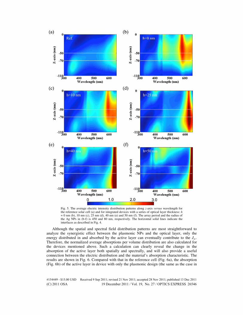
Fig. 5. The average electric intensity distribution patterns along z-axis versus wavelength for the reference solar cell (a) and for integrated devices with a series of optical layer thickness: h = 0 nm (b), 10 nm (c), 25 nm (d), 40 nm (e) and 50 nm (f). The array period and the radius of the Ag NPs in (b-f) is 450 and 80 nm, respectively. The horizontal solid lines indicate the interfaces as described in Fig. 4.
Although the spatial and spectral field distribution patterns are most straightforward to analyze the synergistic effect between the plasmonic NPs and the optical layer, only the energy distributed in and absorbed by the active layer can eventually contribute to the Jsc. Therefore, the normalized average absorptions per volume distribution are also calculated for the devices mentioned above. Such a calculation can clearly reveal the change in the absorption of the active layer both spatially and spectrally, and will also provide a useful connection between the electric distribution and the material’s absorption characteristic. The results are shown in Fig. 6. Compared with that in the reference cell (Fig. 6a), the absorption (Fig. 6b) of the active layer in device with only the plasmonic design (the same as the case in
#154449 - $15.00 USD Received 9 Sep 2011; revised 21 Nov 2011; accepted 28 Nov 2011; published 13 Dec 2011(C) 2011 OSA 19 December 2011 / Vol. 19, No. 27 / OPTICS EXPRESS 26546

Fig. 5b) is obviously enhanced in a spectral range from ~450 to 600 nm; however, in this spectral range the absorption varies violently along the z-axis in such a manner that only that in the “shallow” region is enhanced. This is certainly due to the extremely uneven field distribution for this structure (as shown in Fig. 5b). In contrast, the absorption patterns of the active layer in the integrated devices (Fig. 6c-f) can be more uniform and delocalized so that rather a broad absorption enhancement can be obtain both spatially and spectrally. The best result is given by that shown in Fig. 6d (the design is the same as the case in Fig. 5d), a broadband spectral enhancement from ~400 to ~650 nm is achieved over the entire region of the active layer. By comparing the absorption pattern (Fig. 6d) with the corresponding field distribution (Fig. 5d), we can obtain the key factors for an optimal design: the electric field distribution is 1) spatially manipulated so that it can exclusively concentrated in the active material with the amplitude as large as possible, 2) spectrally engineered to perfectly match the large absorption band of the active material and the high power density range of the solar spectrum (or photon flux).
#154449 - $15.00 USD Received 9 Sep 2011; revised 21 Nov 2011; accepted 28 Nov 2011; published 13 Dec 2011(C) 2011 OSA 19 December 2011 / Vol. 19, No. 27 / OPTICS EXPRESS 26547
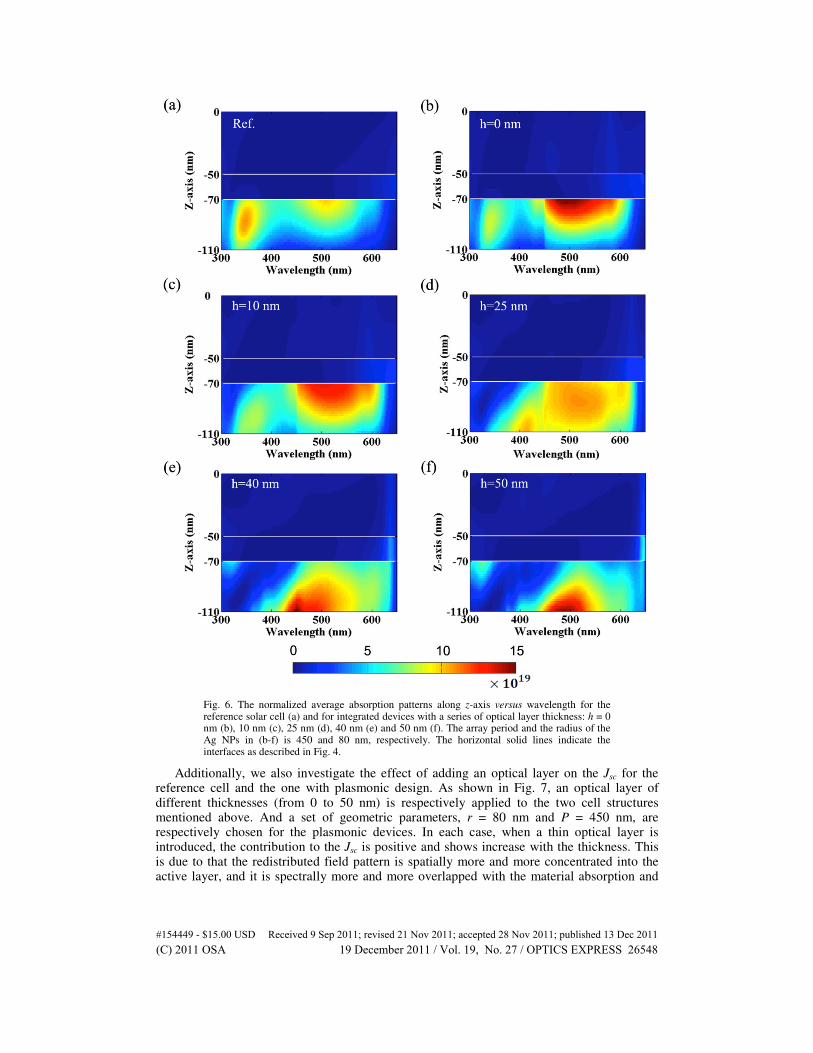
Fig. 6. The normalized average absorption patterns along z-axis versus wavelength for the reference solar cell (a) and for integrated devices with a series of optical layer thickness: h = 0 nm (b), 10 nm (c), 25 nm (d), 40 nm (e) and 50 nm (f). The array period and the radius of the Ag NPs in (b-f) is 450 and 80 nm, respectively. The horizontal solid lines indicate the interfaces as described in Fig. 4.
Additionally, we also investigate the effect of adding an optical layer on the Jsc for the reference cell and the one with plasmonic design. As shown in Fig. 7, an optical layer of different thicknesses (from 0 to 50 nm) is respectively applied to the two cell structures mentioned above. And a set of geometric parameters, r = 80 nm and P = 450 nm, are respectively chosen for the plasmonic devices. In each case, when a thin optical layer is introduced, the contribution to the Jsc is positive and shows increase with the thickness. This is due to that the redistributed field pattern is spatially more and more concentrated into the active layer, and it is spectrally more and more overlapped with the material absorption and
#154449 - $15.00 USD Received 9 Sep 2011; revised 21 Nov 2011; accepted 28 Nov 2011; published 13 Dec 2011(C) 2011 OSA 19 December 2011 / Vol. 19, No. 27 / OPTICS EXPRESS 26548
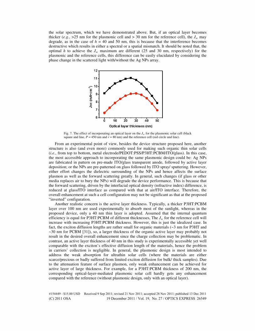
the solar spectrum, which we have demonstrated above. But, if an optical layer becomes thicker (e.g., >25 nm for the plasmonic cell and > 30 nm for the reference cell), the Jsc may degrade, as in the case of h = 40 and 50 nm, this is because that the interference becomes destructive which results in either a spectral or a spatial mismatch. It should be noted that, the optimal h to achieve the Jsc maximum are different (25 and 30 nm, respectively) for the plasmonic and the reference cells, this difference can be easily elucidated by considering the phase change in the scattered light with/without the Ag NPs array.
Fig. 7. The effect of incorporating an optical layer on the Jsc for the plasmonic solar cell (black square and line, P = 450 nm and r = 80 nm) and the reference cell (red circle and line).
From an experimental point of view, besides the device structure proposed here, another structure is also (and even more) commonly used for making such organic thin solar cells (i.e., from top to bottom, metal electrode/PEDOT:PSS/P3HT:PCBM/ITO/glass). In this case, the most accessible approach to incorporating the same plasmonic design could be: Ag NPs are fabricated in pattern on pre-made ITO/glass transparent anode, followed by active layer deposition; or the NPs are pre-patterned on glass followed by ITO spray/ sputtering. However, either effort changes the dielectric surrounding of the NPs and hence affects the surface plasmon as well as the forward scattering greatly. In general, such changes (if glass or other media replaces air to bury the NPs) will degrade the device performance. This is because that the forward scattering, driven by the interfacial optical density (refractive index) difference, is reduced at glass/ITO interface as compared with that at air/ITO interface. Therefore, the overall enhancement at such a cell configuration may not be significant as that at the proposed “inverted” configuration.
Another realistic concern is the active layer thickness. Typically, a thicker P3HT:PCBM layer over 100 nm are used experimentally to absorb most of the sunlight, whereas in the proposed device, only a 40 nm thin layer is adopted. Assumed that the internal quantum efficiency is equal for P3HT:PCBM of different thicknesses, The Jsc for the reference cell will increase with increasing P3HT:PCBM thickness. However, this is just the idealized case. In fact, the exciton diffusion lengths are rather small for organic materials (~3 nm for P3HT and ~30 nm for PCBM [31]), so, a larger thickness of the organic active layer may probably not result in the desired overall enhancement since the charge collection may be problematic. In contrast, an active layer thickness of 40 nm in this study is experimentally accessible yet well comparable with the exciton’s effective diffusion length of the materials, hence the problem in carriers’ collection is negligible. In general, the plasmonic design is most intended to address the weak absorption for ultrathin solar cells (where the materials are either scarce/precious or badly suffered from limited exciton diffusion for bulk/ thick samples). Due to the attenuation feature of surface plasmon, only weak enhancement can be achieved for active layer of large thickness. For example, for a P3HT:PCBM thickness of 200 nm, the corresponding optical-layer-mediated plasmonic solar cell hardly gets any enhancement compared with the reference (without plasmonic design, only with an optical layer).
#154449 - $15.00 USD Received 9 Sep 2011; revised 21 Nov 2011; accepted 28 Nov 2011; published 13 Dec 2011(C) 2011 OSA 19 December 2011 / Vol. 19, No. 27 / OPTICS EXPRESS 26549
It should be pointed out that, even with the carriers’ collection problem ignored, our proposed design with a 40 nm thin active layer (Jsc = 11.0388 mA/cm
2 for P = 475 nm, r = 95
nm, and h = 25 nm) can get a comparable performance to that of the reference cell with a 200 nm thick active layer (Jsc = 12.9657 mA/cm
2). If the limited carriers’ collection in the thick
device is taken into account, our proposed thin cell design will be practically more competitive. The proposed design, although demonstrated here taking P3HT:PCBM as an example, is quite versatile and can be easily extended to other thin solar cell materials. In the cases where scarce or precious materials are used (e.g., indium and tellurium that are commonly used in inorganic thin film solar cells), achieving higher device performance with less active material is exceptionally desired.
Conclusion
In conclusion, we have proposed a new thin solar cell design with plasmonic nanostructures integrated with an optical layer, through incorporating patterned Ag NPs atop of the transparent forward electrode with a conductive optical layer inserted between the active layer and the opaque back electrode. Through this design, a striking and broadband absorption enhancement for the active layer has been achieved. Nicely large Jsc enhancement factors >1.5 with respect to the reference cell can be easily realized within rather a large geometric parameter range, and a maximal Jsc enhancement factor as large as 1.67 can be obtained. The roles of the metallic NPs array and the optical layer as well as their interaction have been carefully studied through investigating the spectral responses, the spatial and spectral electric intensity distributions, and the corresponding absorption patterns. The mechanisms responsible for this large and broad enhancement have been revealed and attributed to a synergistic effect of plasmonically field enhancement and optically interference modulation. Despite the relatively simple structure, such a design is not only compatible with the state-of-art large-scale and inexpensive production techniques (e.g., conventional film deposition for producing optical layer, well-developed imprinting and embossing techniques for generating patterned NPs), it is but also quite versatile and can be easily extended to other thin solar cell systems. Moreover, from a practical viewpoint, such an incorporated optical layer design has many other advantages such as facilitating excitons’ dissociation, improving carrier diffusion/collection, and increasing device’s stability. Therefore, we believe that this new, relatively simple yet efficient “hybrid” thin cell design are very useful to design&produce higher-efficiency and low-cost PVs of the next generation.
Acknowledgments
This work is supported by NSFC under Grant Nos. 11074231, 11004179 and 21121003 as well as by CAS and MOST of China (2011CB921403). N. P. also thanks the support from the Fundamental Research Funds for the Central Universities (FRFCU) under Grant Nos. WK2060030003 and WK2340000011.
#154449 - $15.00 USD Received 9 Sep 2011; revised 21 Nov 2011; accepted 28 Nov 2011; published 13 Dec 2011(C) 2011 OSA 19 December 2011 / Vol. 19, No. 27 / OPTICS EXPRESS 26550


![Enhancing the Angular Sensitivity of Plasmonic Sensors ...biotheory.phys.cwru.edu/PDF/AOM.pdf · ultrasensitive plasmonic biosensors.[29,30] A plasmonic nanorod metamaterial (Type](https://img.pdfslide.net/doc/110x75/5fcdd2c6db367d06a677e7be/enhancing-the-angular-sensitivity-of-plasmonic-sensors-ultrasensitive-plasmonic.jpg)