Embed Size (px)
Citation preview
Broadband and wide angle infrared wire-grid polarizer
Ming Dai,1 Weiwei Wan,1 Xueyi Zhu,1 Baosheng Song,1 Xiaoping Liu,1 Minghui Lu,1,* Bo Cui,2 and Yanfeng Chen1
1National Laboratory of Solid State Microstructures, College of Engineering and Applied Sciences, Nanjing University, Nanjing 210093, China
2Department of Electrical and Computer Engineering, Waterloo Institute for Nanotechnology, University of Waterloo, Waterloo, ON N2L3G1, Canada
Abstract: An infrared polarizer consisting of metal-insulator-metal (MIM) gratings is designed with transmittance exceeding 85% and polarization extinction ratio (ER) higher than 70 dB in the wavelength range from 1.5 to 8 μm. Moreover, the polarizer retains excellent performance even when the incident angle increases to as large as 80°. The MIM gratings support magnetic polariton (MP) in the near-infrared regime and operate non-resonantly in the mid-infrared regime, both of which result in the advantages of high extinction ratio, broadband, and wide angle. The proposed structure can find applications in polarizer, beam-splitter, filter, and isolator in the infrared range.
©2015 Optical Society of America
OCIS codes: (230.5440) Polarization-selective devices; (050.2770) Gratings.
References and links 1. X.-J. Yu and H.-S. Kwok, “Application of wire-grid polarizers to projection displays,” Appl. Opt. 42(31), 6335–
6341 (2003). 2. F. B. McCormick, F. A. Tooley, T. J. Cloonan, J. L. Brubaker, A. L. Lentine, R. L. Morrison, S. J. Hinterlong,
M. J. Herron, S. L. Walker, and J. M. Sasian, “Experimental investigation of a free-space optical switching network by using symmetric self-electro-optic-effect devices,” Appl. Opt. 31(26), 5431–5446 (1992).
3. V. Gruev, R. Perkins, and T. York, “CCD polarization imaging sensor with aluminum nanowire optical filters,” Opt. Express 18(18), 19087–19094 (2010).
4. J. J. Wang, L. Chen, X. Liu, P. Sciortino, F. Liu, F. Walters, and X. Deng, “30-nm-wide aluminum nanowire grid for ultrahigh contrast and transmittance polarizers made by UV-nanoimprint lithography,” Appl. Phys. Lett. 89(14), 141105 (2006).
5. L. Deng, J. Teng, L. Zhang, Q. Wu, H. Liu, X. Zhang, and S. Chua, “Extremely high extinction ratio terahertz broadband polarizer using bilayer subwavelength metal wire-grid structure,” Appl. Phys. Lett. 101(1), 011101 (2012).
6. Z. Y. Yang and Y. F. Lu, “Broadband nanowire-grid polarizers in ultraviolet-visible-near-infrared regions,” Opt. Express 15(15), 9510–9519 (2007).
7. X. L. Liu, B. Zhao, and Z. M. Zhang, “Wide-angle near infrared polarizer with extremely high extinction ratio,” Opt. Express 21(9), 10502–10510 (2013).
8. L. Sun, Z.-H. Lv, W. Wu, W.-T. Liu, and J.-M. Yuan, “Double-grating polarizer for terahertz radiation with high extinction ratio,” Appl. Opt. 49(11), 2066–2071 (2010).
9. C. Cheng, J. Chen, D.-J. Shi, Q.-Y. Wu, F.-F. Ren, J. Xu, Y.-X. Fan, J. Ding, and H.-T. Wang, “Physical mechanism of extraordinary electromagnetic transmission in dual-metallic grating structures,” Phys. Rev. B 78(7), 075406 (2008).
10. J. Nie, H. Li, and W. Liu, “Robust broadband optical transmission realized in a dual-metallic gratings structure,” IEEE Photonics J. 6(4), 2700208 (2014).
11. J. Hao, C.-W. Qiu, M. Qiu, and S. Zouhdi, “Design of an ultrathin broadband transparent and high-conductive screen using plasmonic nanostructures,” Opt. Lett. 37(23), 4955–4957 (2012).
12. L. Zhang, J. Hao, H. Ye, S. P. Yeo, M. Qiu, S. Zouhdi, and C. W. Qiu, “Theoretical realization of robust broadband transparency in ultrathin seamless nanostructures by dual blackbodies for near infrared light,” Nanoscale 5(8), 3373–3379 (2013).
13. G. Subramania, S. Foteinopoulou, and I. Brener, “Nonresonant broadband funneling of light via ultrasubwavelength channels,” Phys. Rev. Lett. 107(16), 163902 (2011).
14. H. Shen and B. Maes, “Enhanced optical transmission through tapered metallic gratings,” Appl. Phys. Lett. 100(24), 241104 (2012).
#234644 - $15.00 USD Received 13 Feb 2015; revised 28 Apr 2015; accepted 30 May 2015; published 3 Jun 2015 (C) 2015 OSA 15 Jun 2015 | Vol. 23, No. 12 | DOI:10.1364/OE.23.015390 | OPTICS EXPRESS 15390
15. L. Wang and Z. M. Zhang, “Effect of magnetic polaritons on the radiative properties of double-layer nanoslit arrays,” J. Opt. Soc. Am. B 27(12), 2595–2604 (2010).
16. X. Liu, B. Zhao, and Z. Zhang, “Blocking-assisted infrared transmission of subwavelength metallic gratings by graphene,” J. Opt. 17(3), 035004 (2015).
17. W. Cai, U. K. Chettiar, H.-K. Yuan, V. C. de Silva, A. V. Kildishev, V. P. Drachev, and V. M. Shalaev, “Metamagnetics with rainbow colors,” Opt. Express 15(6), 3333–3341 (2007).
18. A. Alù and N. Engheta, “Optical nanotransmission lines: synthesis of planar left-handed metamaterials in the infrared and visible regimes,” J. Opt. Soc. Am. B 23(3), 571–583 (2006).
19. A. Alù, G. D’Aguanno, N. Mattiucci, and M. J. Bloemer, “Plasmonic Brewster angle: broadband extraordinary transmission through optical gratings,” Phys. Rev. Lett. 106(12), 123902 (2011).
20. X.-R. Huang, R.-W. Peng, and R.-H. Fan, “Making metals transparent for white light by spoof surface plasmons,” Phys. Rev. Lett. 105(24), 243901 (2010).
1. Introduction
Polarizers are essential optical elements and have been widely used in optical display, optical switches and imaging systems [1–3]. Compared with conventional bulky prism polarizers, metal wire grid structure is compact and planar, which can be used to make integration-capable and thin-film-type polarizers. Besides miniaturization, the good performance of a polarizer is also characterized by high transmittance for one polarization and low transmittance for another polarization, as well as broad bandwidth, wide angular tolerance, and easy fabrication.
The extinction ratio (ER) of a wire-grid polarizer can be defined as 10 × log10 (TTM /TTE), where TTM and TTE is the intensity transmittance of TM and TE polarized wave, respectively. Since TTM cannot exceed 100%, the most effective approach to increase ER is to decrease TTE. It is known that increasing thickness of metallic wire could dramatically decrease TTE and hence increase extinction ratio [4, 5]. However, this would also induce an undesired drop of TTM. The dual-metallic grating (DMG) structure was proposed to achieve both high transmittance and large ER [6–9]. By introducing the DMG structures in both sides of CaF2 substrate, a broadband polarizer was designed with average extinction ratio over 70 dB and transmittance over 64% in the range of 0.3 to 5µm [6]. Recently, a DMG structure with lateral half period shift is proposed and theoretically demonstrated to have extremely high extinction ratio of 160 dB [7]. However, the precise control of positions of the double gratings on two sides of dielectric layer would inevitably introduce new challenge to practical fabrication. Thus, an easy-fabrication wire-grid polarizer with good performance in infrared range is still highly demanded.
On the other hand, many of the wire grid polarizers works are based on the resonance nature of one dimensional metallic grating [7]. However, resonant phenomena unavoidably have a narrow spectral bandwidth. One approach to control the bandwidth is to engineer the interaction between the resonance modes. By exploiting the coupling between different-order Fabry-Perot (FP) resonances [9] or magnetic (plasmonic) polaritons (MP) [10], a broadened bandwidth can be achieved in DMGs [9–12]. Another approach is to introduce a non-resonant mechanism, which can also render the proposed metallic structures functional in a broad wavelength range [13, 14].
In this paper, we propose metal-insulator-metal (MIM) sandwich structures which stand on one side of a substrate without lateral shift. Compared with the two-side double grating polarizers [6], our proposed polarizer is more practical to fabricate and still maintains high performance, with TM transmittance larger than 85% and extinction ratio exceeding 70 dB for a broad infrared wavelength range (1.5-8 µm). Moreover, the performance of high transmittance and extinction ratio still holds with the incident angle increased to 80°. The wide-angle broadband high transmittance results from the magnetic (plasmonic) polariton (MP) in near infrared regime supported by MIM structures and the non-resonant mechanism occurring in the long-wavelength regime. The broadband functionality (from near-infrared to mid- infrared) allows for flexible utilization in many applications of optical communications, molecular fingerprinting or sensing.
#234644 - $15.00 USD Received 13 Feb 2015; revised 28 Apr 2015; accepted 30 May 2015; published 3 Jun 2015 (C) 2015 OSA 15 Jun 2015 | Vol. 23, No. 12 | DOI:10.1364/OE.23.015390 | OPTICS EXPRESS 15391
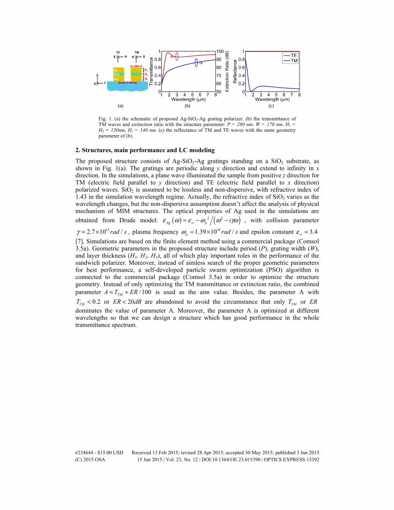
Fig. 1. (a) the schematic of proposed Ag-SiO2-Ag grating polarizer. (b) the transmittance of TM waves and extinction ratio with the structure parameter: P = 280 nm, W = 170 nm, H1 = H3 = 150nm, H2 = 140 nm. (c) the reflectance of TM and TE waves with the same geometry parameter of (b).
2. Structures, main performance and LC modeling
The proposed structure consists of Ag-SiO2-Ag gratings standing on a SiO2 substrate, as shown in Fig. 1(a). The gratings are periodic along y direction and extend to infinity in x direction. In the simulations, a plane wave illuminated the sample from positive z direction for TM (electric field parallel to y direction) and TE (electric field parallel to x direction) polarized waves. SiO2 is assumed to be lossless and non-dispersive, with refractive index of 1.43 in the simulation wavelength regime. Actually, the refractive index of SiO2 varies as the wavelength changes, but the non-dispersive assumption doesn’t affect the analysis of physical mechanism of MIM structures. The optical properties of Ag used in the simulations are
obtained from Drude model: ( ) ( )2 2Ag p iε ω ε ω ω γω∞= − − , with collision parameter
132.7 10 /rad sγ = × , plasma frequency 161.39 10 /p rad sω = × and epsilon constant 3.4ε∞ =
[7]. Simulations are based on the finite element method using a commercial package (Comsol 3.5a). Geometric parameters in the proposed structure include period (P), grating width (W), and layer thickness (H1, H2, H3), all of which play important roles in the performance of the sandwich polarizer. Moreover, instead of aimless search of the proper geometric parameters for best performance, a self-developed particle swarm optimization (PSO) algorithm is connected to the commercial package (Comsol 3.5a) in order to optimize the structure geometry. Instead of only optimizing the TM transmittance or extinction ratio, the combined parameter /100TMA T ER= + is used as the aim value. Besides, the parameter A with
0.2TMT < or 20ER dB< are abandoned to avoid the circumstance that only TMT or ER dominates the value of parameter A. Moreover, the parameter A is optimized at different wavelengths so that we can design a structure which has good performance in the whole transmittance spectrum.
#234644 - $15.00 USD Received 13 Feb 2015; revised 28 Apr 2015; accepted 30 May 2015; published 3 Jun 2015 (C) 2015 OSA 15 Jun 2015 | Vol. 23, No. 12 | DOI:10.1364/OE.23.015390 | OPTICS EXPRESS 15392
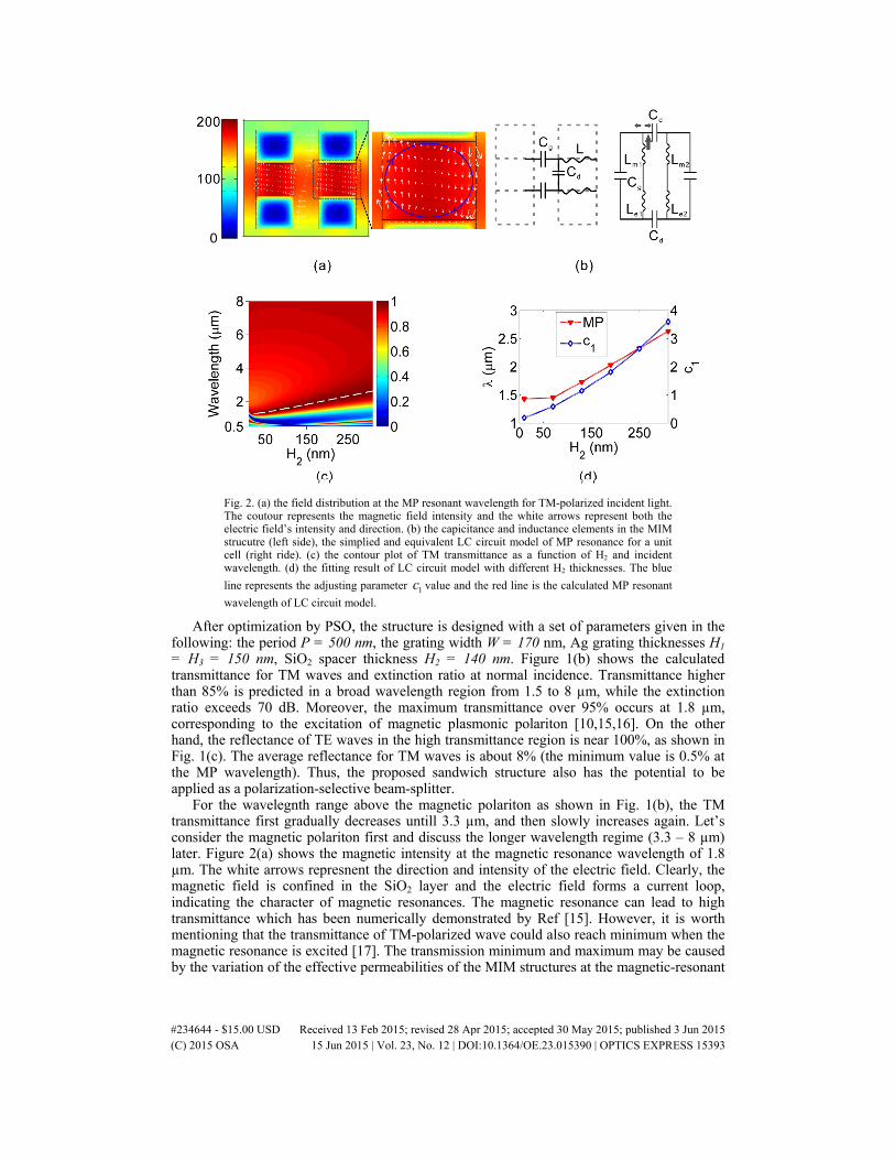
Fig. 2. (a) the field distribution at the MP resonant wavelength for TM-polarized incident light. The coutour represents the magnetic field intensity and the white arrows represent both the electric field’s intensity and direction. (b) the capicitance and inductance elements in the MIM strucutre (left side), the simplied and equivalent LC circuit model of MP resonance for a unit cell (right ride). (c) the contour plot of TM transmittance as a function of H2 and incident wavelength. (d) the fitting result of LC circuit model with different H2 thicknesses. The blue
line represents the adjusting parameter 1c value and the red line is the calculated MP resonant
wavelength of LC circuit model.
After optimization by PSO, the structure is designed with a set of parameters given in the following: the period P = 500 nm, the grating width W = 170 nm, Ag grating thicknesses H1 = H3 = 150 nm, SiO2 spacer thickness H2 = 140 nm. Figure 1(b) shows the calculated transmittance for TM waves and extinction ratio at normal incidence. Transmittance higher than 85% is predicted in a broad wavelength region from 1.5 to 8 µm, while the extinction ratio exceeds 70 dB. Moreover, the maximum transmittance over 95% occurs at 1.8 µm, corresponding to the excitation of magnetic plasmonic polariton [10,15,16]. On the other hand, the reflectance of TE waves in the high transmittance region is near 100%, as shown in Fig. 1(c). The average reflectance for TM waves is about 8% (the minimum value is 0.5% at the MP wavelength). Thus, the proposed sandwich structure also has the potential to be applied as a polarization-selective beam-splitter.
For the wavelegnth range above the magnetic polariton as shown in Fig. 1(b), the TM transmittance first gradually decreases untill 3.3 µm, and then slowly increases again. Let’s consider the magnetic polariton first and discuss the longer wavelength regime (3.3 – 8 µm) later. Figure 2(a) shows the magnetic intensity at the magnetic resonance wavelength of 1.8 µm. The white arrows represnent the direction and intensity of the electric field. Clearly, the magnetic field is confined in the SiO2 layer and the electric field forms a current loop, indicating the character of magnetic resonances. The magnetic resonance can lead to high transmittance which has been numerically demonstrated by Ref [15]. However, it is worth mentioning that the transmittance of TM-polarized wave could also reach minimum when the magnetic resonance is excited [17]. The transmission minimum and maximum may be caused by the variation of the effective permeabilities of the MIM structures at the magnetic-resonant
#234644 - $15.00 USD Received 13 Feb 2015; revised 28 Apr 2015; accepted 30 May 2015; published 3 Jun 2015 (C) 2015 OSA 15 Jun 2015 | Vol. 23, No. 12 | DOI:10.1364/OE.23.015390 | OPTICS EXPRESS 15393
wavelengths. The effective permeability is negative / positive at the transmittance minimum/maximum wavelength, thus the impedance of the magnetic resonance cannot/can match with that of the outgoing dielectric medium, resulting in the transmission minimum/maximum. Note that parts of the magnetic field also spreads out into the gap region, which results from the low quality factor of the magnetic resonance. Usually the thicker the spacer is, the lower the quality factor of the mode is [10]. The lower quality factor of the magnetic resonance has larger full width at half maximum (FWHM), leading to a broadband polarizer.
To better understand and explore the magnetic resonance at the transmittance maximum wavelength, a LC circuit model was developed. Equivalent capacitances and inductances can be used to analyze one unit cell of the MIM structure. Cg denotes the gap capacitance in the air gap of neighbouring grating wires. Cd represents the dielectric capacitance between the two layers of metal nano-ribbons. L is the sum inductance of Lm and Le. Here Lm is the inductance of two metal strips separated by distance H2, and Le is the inductance originating from drifting electrons. The whole LC circuit can be simplied as Fig. 2(b). The expression of these LC circuit elements can be described as:
0 1 1 0
2
, rg d
H I c WIC C
P W H
ε ε ε= =
− (1)
0 22
0
,2m e
p
WH WL L
I Aδ
με ω
= = (2)
m eL L L= + (3)
where 0ε and 0μ are the permittivity and permeability of vacuum, respectively, and rε is the relative permittivity of SiO2. I is the grating’s length in x direction, which could be cancelled in the final calculation. It is assumed that all induced electric current in the metal flows within a penetration depth / 4δ λ πκ= , where κ is the extinction coefficient of Ag. A Iδ δ= is the cross-section area of the flow of induced current. To take the non-uniform charge distribution into account, the coefficient 1c is introduced, which is often treated as adjusting parameter of LC circuit model [7, 10, 15].
Based on the simplified LC circuit model and the basic elements defined above, the total impedance of one unit cell of the MIM gratings can be written as:
2
1( ) 2 2
1g
d
g
C L
total CC L d g
Z Z j LZ Z
Z Z j C LC
ωωω ω
= + = ++ −
(4)
Let ( ) 0totalZ ω = , we can deduce the magnetic resonance wavelength MPλ as:
02 (C C )MP m dc Lλ π= + (5)
where 0c is the speed of light in vacuum. Figure 2(c) shows the transmittance spectra with different thicknesses of the SiO2 spacer.
The white dashed line indicates the MP wavelength whose transmittance always exceeds 95% if H2 is restricted between 10 nm and 310 nm. Even for the case of H2 = 10 nm, the minimum transmittance is still acceptably large (> 75%). Six different points in Fig. 2(c) are selected to verify the LC circuit model and the results are shown in Fig. 2(d). The blue and red curves represent the adjusting parameter 1c value and the calculated MP wavelength by LC circuit model, repectively. The MP wavelengths of LC circuit model match well with the simulation results. It is worth mentioning that the adjusting parameter 1c regarding the non-uniform charge distribution is growing as the increase of H2. This is consistent with the field
#234644 - $15.00 USD Received 13 Feb 2015; revised 28 Apr 2015; accepted 30 May 2015; published 3 Jun 2015 (C) 2015 OSA 15 Jun 2015 | Vol. 23, No. 12 | DOI:10.1364/OE.23.015390 | OPTICS EXPRESS 15394
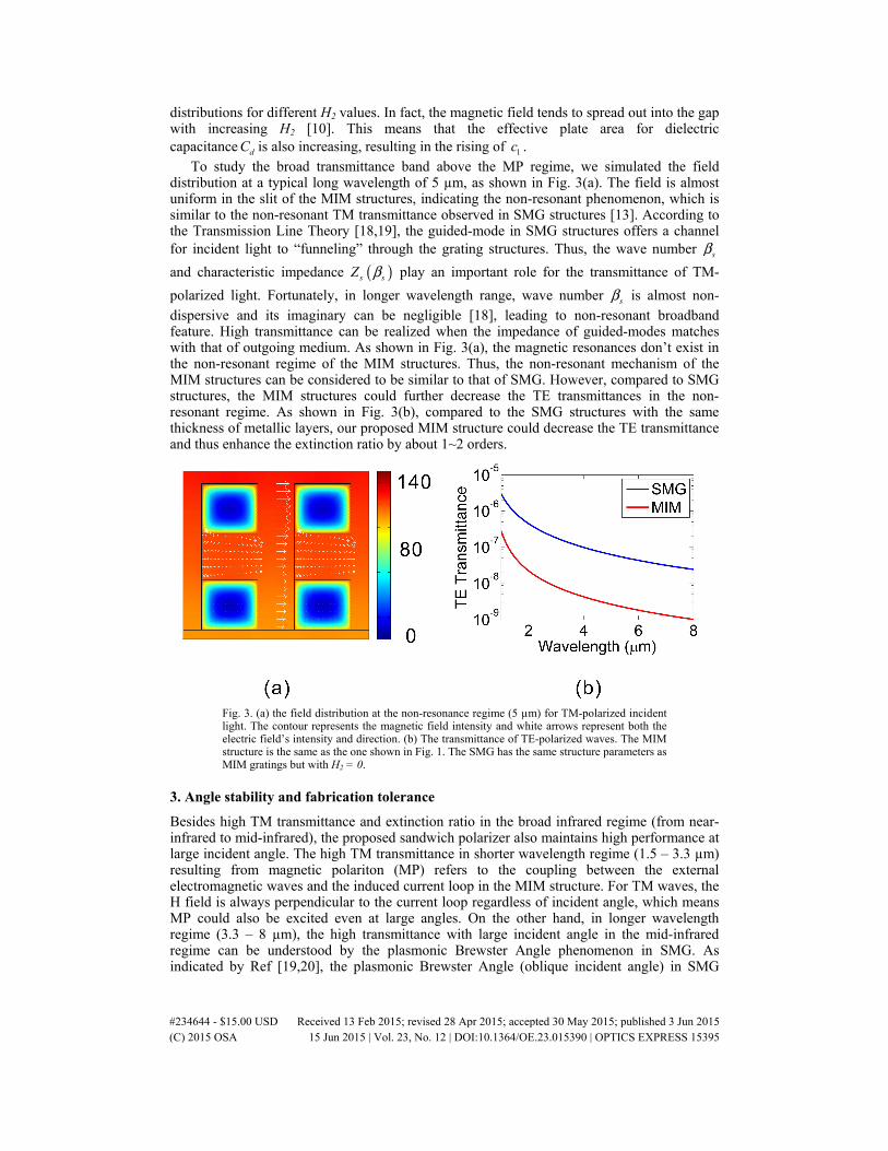
distributions for different H2 values. In fact, the magnetic field tends to spread out into the gap with increasing H2 [10]. This means that the effective plate area for dielectric capacitance dC is also increasing, resulting in the rising of 1c .
To study the broad transmittance band above the MP regime, we simulated the field distribution at a typical long wavelength of 5 µm, as shown in Fig. 3(a). The field is almost uniform in the slit of the MIM structures, indicating the non-resonant phenomenon, which is similar to the non-resonant TM transmittance observed in SMG structures [13]. According to the Transmission Line Theory [18,19], the guided-mode in SMG structures offers a channel for incident light to “funneling” through the grating structures. Thus, the wave number sβ
and characteristic impedance ( )s sZ β play an important role for the transmittance of TM-
polarized light. Fortunately, in longer wavelength range, wave number sβ is almost non-dispersive and its imaginary can be negligible [18], leading to non-resonant broadband feature. High transmittance can be realized when the impedance of guided-modes matches with that of outgoing medium. As shown in Fig. 3(a), the magnetic resonances don’t exist in the non-resonant regime of the MIM structures. Thus, the non-resonant mechanism of the MIM structures can be considered to be similar to that of SMG. However, compared to SMG structures, the MIM structures could further decrease the TE transmittances in the non-resonant regime. As shown in Fig. 3(b), compared to the SMG structures with the same thickness of metallic layers, our proposed MIM structure could decrease the TE transmittance and thus enhance the extinction ratio by about 1~2 orders.
Fig. 3. (a) the field distribution at the non-resonance regime (5 µm) for TM-polarized incident light. The contour represents the magnetic field intensity and white arrows represent both the electric field’s intensity and direction. (b) The transmittance of TE-polarized waves. The MIM structure is the same as the one shown in Fig. 1. The SMG has the same structure parameters as MIM gratings but with H2 = 0.
3. Angle stability and fabrication tolerance
Besides high TM transmittance and extinction ratio in the broad infrared regime (from near-infrared to mid-infrared), the proposed sandwich polarizer also maintains high performance at large incident angle. The high TM transmittance in shorter wavelength regime (1.5 – 3.3 µm) resulting from magnetic polariton (MP) refers to the coupling between the external electromagnetic waves and the induced current loop in the MIM structure. For TM waves, the H field is always perpendicular to the current loop regardless of incident angle, which means MP could also be excited even at large angles. On the other hand, in longer wavelength regime (3.3 – 8 µm), the high transmittance with large incident angle in the mid-infrared regime can be understood by the plasmonic Brewster Angle phenomenon in SMG. As indicated by Ref [19,20], the plasmonic Brewster Angle (oblique incident angle) in SMG
#234644 - $15.00 USD Received 13 Feb 2015; revised 28 Apr 2015; accepted 30 May 2015; published 3 Jun 2015 (C) 2015 OSA 15 Jun 2015 | Vol. 23, No. 12 | DOI:10.1364/OE.23.015390 | OPTICS EXPRESS 15395
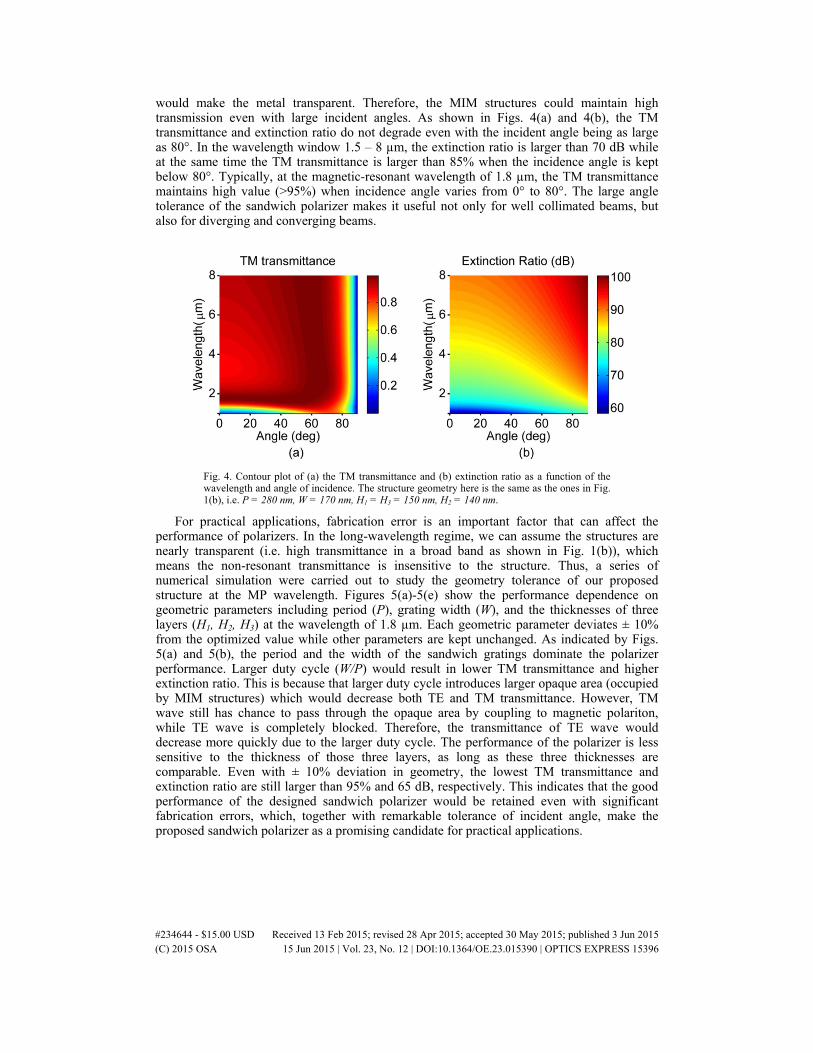
would make the metal transparent. Therefore, the MIM structures could maintain high transmission even with large incident angles. As shown in Figs. 4(a) and 4(b), the TM transmittance and extinction ratio do not degrade even with the incident angle being as large as 80°. In the wavelength window 1.5 – 8 µm, the extinction ratio is larger than 70 dB while at the same time the TM transmittance is larger than 85% when the incidence angle is kept below 80°. Typically, at the magnetic-resonant wavelength of 1.8 µm, the TM transmittance maintains high value (>95%) when incidence angle varies from 0° to 80°. The large angle tolerance of the sandwich polarizer makes it useful not only for well collimated beams, but also for diverging and converging beams.
Fig. 4. Contour plot of (a) the TM transmittance and (b) extinction ratio as a function of the wavelength and angle of incidence. The structure geometry here is the same as the ones in Fig. 1(b), i.e. P = 280 nm, W = 170 nm, H1 = H3 = 150 nm, H2 = 140 nm.
For practical applications, fabrication error is an important factor that can affect the performance of polarizers. In the long-wavelength regime, we can assume the structures are nearly transparent (i.e. high transmittance in a broad band as shown in Fig. 1(b)), which means the non-resonant transmittance is insensitive to the structure. Thus, a series of numerical simulation were carried out to study the geometry tolerance of our proposed structure at the MP wavelength. Figures 5(a)-5(e) show the performance dependence on geometric parameters including period (P), grating width (W), and the thicknesses of three layers (H1, H2, H3) at the wavelength of 1.8 µm. Each geometric parameter deviates ± 10% from the optimized value while other parameters are kept unchanged. As indicated by Figs. 5(a) and 5(b), the period and the width of the sandwich gratings dominate the polarizer performance. Larger duty cycle (W/P) would result in lower TM transmittance and higher extinction ratio. This is because that larger duty cycle introduces larger opaque area (occupied by MIM structures) which would decrease both TE and TM transmittance. However, TM wave still has chance to pass through the opaque area by coupling to magnetic polariton, while TE wave is completely blocked. Therefore, the transmittance of TE wave would decrease more quickly due to the larger duty cycle. The performance of the polarizer is less sensitive to the thickness of those three layers, as long as these three thicknesses are comparable. Even with ± 10% deviation in geometry, the lowest TM transmittance and extinction ratio are still larger than 95% and 65 dB, respectively. This indicates that the good performance of the designed sandwich polarizer would be retained even with significant fabrication errors, which, together with remarkable tolerance of incident angle, make the proposed sandwich polarizer as a promising candidate for practical applications.
#234644 - $15.00 USD Received 13 Feb 2015; revised 28 Apr 2015; accepted 30 May 2015; published 3 Jun 2015 (C) 2015 OSA 15 Jun 2015 | Vol. 23, No. 12 | DOI:10.1364/OE.23.015390 | OPTICS EXPRESS 15396
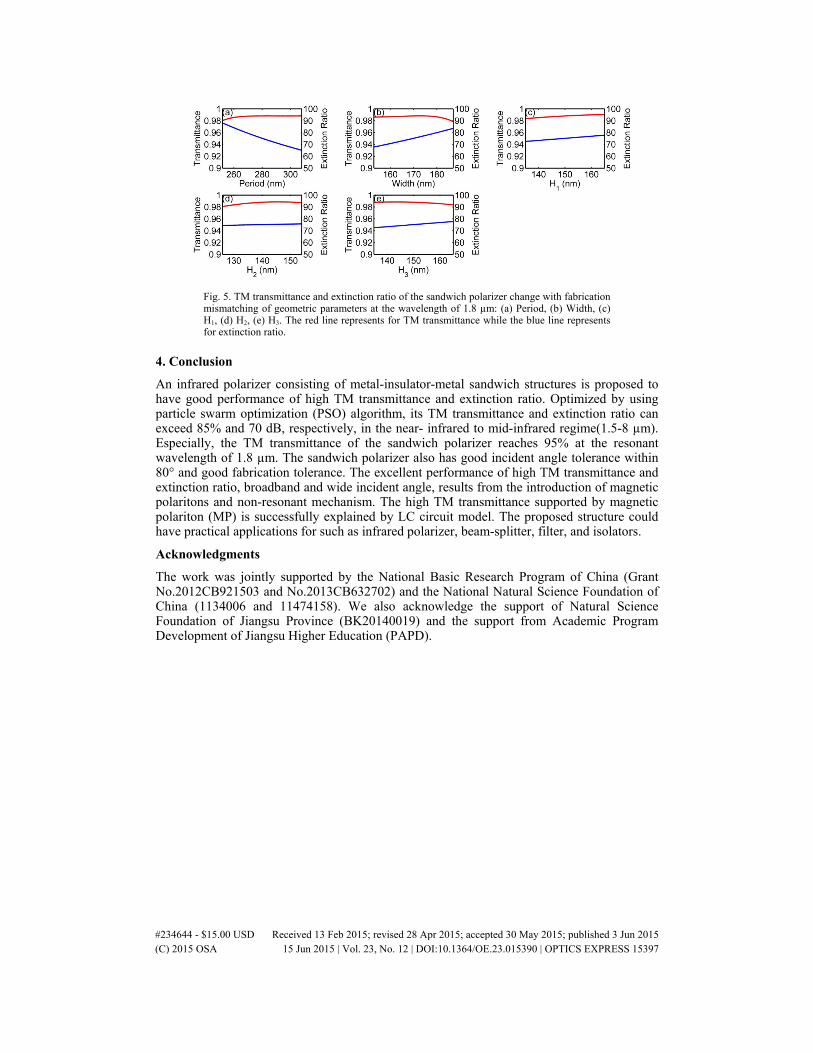
Fig. 5. TM transmittance and extinction ratio of the sandwich polarizer change with fabrication mismatching of geometric parameters at the wavelength of 1.8 µm: (a) Period, (b) Width, (c) H1, (d) H2, (e) H3. The red line represents for TM transmittance while the blue line represents for extinction ratio.
4. Conclusion
An infrared polarizer consisting of metal-insulator-metal sandwich structures is proposed to have good performance of high TM transmittance and extinction ratio. Optimized by using particle swarm optimization (PSO) algorithm, its TM transmittance and extinction ratio can exceed 85% and 70 dB, respectively, in the near- infrared to mid-infrared regime(1.5-8 µm). Especially, the TM transmittance of the sandwich polarizer reaches 95% at the resonant wavelength of 1.8 µm. The sandwich polarizer also has good incident angle tolerance within 80° and good fabrication tolerance. The excellent performance of high TM transmittance and extinction ratio, broadband and wide incident angle, results from the introduction of magnetic polaritons and non-resonant mechanism. The high TM transmittance supported by magnetic polariton (MP) is successfully explained by LC circuit model. The proposed structure could have practical applications for such as infrared polarizer, beam-splitter, filter, and isolators.
Acknowledgments
The work was jointly supported by the National Basic Research Program of China (Grant No.2012CB921503 and No.2013CB632702) and the National Natural Science Foundation of China (1134006 and 11474158). We also acknowledge the support of Natural Science Foundation of Jiangsu Province (BK20140019) and the support from Academic Program Development of Jiangsu Higher Education (PAPD).
#234644 - $15.00 USD Received 13 Feb 2015; revised 28 Apr 2015; accepted 30 May 2015; published 3 Jun 2015 (C) 2015 OSA 15 Jun 2015 | Vol. 23, No. 12 | DOI:10.1364/OE.23.015390 | OPTICS EXPRESS 15397