Embed Size (px)
Citation preview
Brushless DC Motor Flash MCU
HT45FM30
Revision: V.1.20 Date: De�e��e� 1�� 201�De�e��e� 1�� 201�
Rev. 1.20 2 De�e��e� 1�� 201� Rev. 1.20 3 De�e��e� 1�� 201�
HT45FM30Brushless DC Motor Flash MCU
Table of Contents
Features ............................................................................................................. 7CPU Featu�es .......................................................................................................................... 7Pe�iphe�al Featu�es .................................................................................................................. 7
General Description .......................................................................................... 8Block Diagram ................................................................................................... 9Pin Assignment ............................................................................................... 10Pin Description ............................................................................................... 11Absolute Maximum Ratings ........................................................................... 13D.C. Characteristics ........................................................................................ 14A.C. Characteristics ........................................................................................ 15Power-on Reset Characteristics .................................................................... 15ADC Electrical Characteristics ...................................................................... 15Comparator Electrical Characteristics ......................................................... 16OPA Electrical Characteristics ...................................................................... 16Shunt Regulator Electrical Characteristics .................................................. 16System Architecture ....................................................................................... 17
Clo�king and Pipelining .......................................................................................................... 17P�og�a� Counte� .................................................................................................................... 18Sta�k ...................................................................................................................................... 18A�ith�eti� and Logi� Unit – ALU ............................................................................................ 19
Flash Program Memory .................................................................................. 19St�u�tu�e ................................................................................................................................. 19Spe�ial Ve�to�s ...................................................................................................................... 20Look-up Ta�le ......................................................................................................................... 20Ta�le P�og�a� Exa�ple ......................................................................................................... 20In Ci��uit P�og�a��ing .......................................................................................................... 21
RAM Data Memory .......................................................................................... 22St�u�tu�e ................................................................................................................................. 22
Special Function Register Description ......................................................... 24Indi�e�t Add�essing Registe�s – IAR0� IAR1 .......................................................................... 24Me�o�y Pointe�s – MP0� MP1 ............................................................................................... 24Bank Pointe� – BP .................................................................................................................. 25A��u�ulato� – ACC ................................................................................................................ 2�P�og�a� Counte� Low Registe� – PCL ................................................................................... 2�Look-up Ta�le Registe�s – TBLP� TBHP� TBLH ...................................................................... 2�Status Registe� – STATUS ..................................................................................................... 2�
Rev. 1.20 2 De�e��e� 1�� 201� Rev. 1.20 3 De�e��e� 1�� 201�
HT45FM30Brushless DC Motor Flash MCU
EEPROM Data Memory ................................................................................... 28EEPROM Data Me�o�y St�u�tu�e ......................................................................................... 28EEPROM Cont�ol Registe�s ................................................................................................... 28Reading Data f�o� the EEPROM .......................................................................................... 30W�iting Data to the EEPROM ................................................................................................. 30W�ite P�ote�tion ...................................................................................................................... 30EEPROM Inte��upt ................................................................................................................. 30P�og�a��ing Conside�ations ................................................................................................. 31P�og�a��ing Exa�ples ......................................................................................................... 31
Oscillator ......................................................................................................... 32Syste� Os�illato� Ove�view ................................................................................................... 32System Clock Configurations ................................................................................................. 32
Operating Modes ............................................................................................ 34Syste� Ope�ation Modes ....................................................................................................... 34Cont�ol Registe� ..................................................................................................................... 35Os�illato� Wake-up Ti�e ........................................................................................................ 3�Ope�ating Mode Swit�hing and Wake-up ............................................................................... 37NORMAL Mode to SLOW Mode Swit�hing ............................................................................ 37SLOW Mode to NORMAL Mode Swit�hing ............................................................................ 39Ente�ing the SLEEP Mode ..................................................................................................... 39Ente�ing the IDLE0 Mode ....................................................................................................... 39Ente�ing the IDLE1 Mode ....................................................................................................... 39Stand�y Cu��ent Conside�ations ............................................................................................ 40Wake-up ................................................................................................................................. 40
Watchdog Timer .............................................................................................. 41Wat�hdog Ti�e� Clo�k Sou��e ............................................................................................... 41Wat�hdog Ti�e� Cont�ol Registe� .......................................................................................... 41Wat�hdog Ti�e� Ope�ation .................................................................................................... 42
Reset and Initialisation ................................................................................... 43Reset Fun�tions ..................................................................................................................... 43Reset Initial Conditions .......................................................................................................... 44
Input/Output Ports .......................................................................................... 47Pin-sha�ed p�io�ity .................................................................................................................. 48Pull-high Resisto�s ................................................................................................................. 48Po�t A Wake-up ...................................................................................................................... 49I/O Po�t Cont�ol Registe�s ...................................................................................................... 50Pin-�e�apping Fun�tions ....................................................................................................... 51Pin-�e�apping Registe�s ........................................................................................................ 51I/O Pin St�u�tu�es ................................................................................................................... 53P�og�a��ing Conside�ations ................................................................................................. 54
Rev. 1.20 4 De�e��e� 1�� 201� Rev. 1.20 5 De�e��e� 1�� 201�
HT45FM30Brushless DC Motor Flash MCU
Timer Modules – TM ....................................................................................... 54Int�odu�tion ........................................................................................................................... 54TM Ope�ation ......................................................................................................................... 55TM Clo�k Sou��e .................................................................................................................... 55TM Inte��upts .......................................................................................................................... 55TM Exte�nal Pins .................................................................................................................... 55TM Input/Output Pin Cont�ol Registe�s .................................................................................. 5�P�og�a��ing Conside�ations ................................................................................................. 57
Compact Type TM – CTM ............................................................................... 58Co�pa�t TM Ope�ation .......................................................................................................... 58Co�pa�t Type TM Registe� Des��iption................................................................................. 58Co�pa�t Type TM Ope�ating Modes ..................................................................................... �2Co�pa�e Mat�h Output Mode ................................................................................................ �2Ti�e�/Counte� Mode .............................................................................................................. �5PWM Output Mode ................................................................................................................. �5
Standard Type TM – STM ............................................................................... 68Standa�d TM Ope�ation .......................................................................................................... �8Standa�d Type TM Registe� Des��iption ................................................................................ �9Standa�d Type TM Ope�ating Modes ..................................................................................... 72Co�pa�e Output Mode ........................................................................................................... 72Ti�e�/Counte� Mode .............................................................................................................. 75PWM Output Mode ................................................................................................................. 75Single Pulse Mode ................................................................................................................. 78Captu�e Input Mode ............................................................................................................... 80
Analog to Digital Converter ........................................................................... 82A/D Ove�view ......................................................................................................................... 82A/D Conve�te� Registe� Des��iption ....................................................................................... 82A/D Conve�te� Data Registe�s – ADRL� ADRH ...................................................................... 83A/D Conve�te� Cont�ol Registe�s – ADCR0� ADCR1� ACERL ................................................ 83A/D Ope�ation ........................................................................................................................ 8�A/D Input Pins ........................................................................................................................ 87Su��a�y of A/D Conve�sion Steps ........................................................................................ 88P�og�a��ing Conside�ations ................................................................................................. 89A/D T�ansfe� Fun�tion ............................................................................................................ 89A/D P�og�a��ing Exa�ple .................................................................................................... 90
Operational Amplifier – OPA .......................................................................... 92Operational Amplifier Registers .............................................................................................. 92Operational Amplifier Operation ............................................................................................. 92Operational Amplifier Offset Cancellation function ................................................................. 93
Rev. 1.20 4 De�e��e� 1�� 201� Rev. 1.20 5 De�e��e� 1�� 201�
HT45FM30Brushless DC Motor Flash MCU
Comparators ................................................................................................... 94Co�pa�ato� Ope�ation ........................................................................................................... 94Co�pa�ato� Registe�s ............................................................................................................ 95Co�pa�ato� Inte��upt .............................................................................................................. 99P�og�a��ing Conside�ations ................................................................................................. 99
Digital to Analog Converter – DAC .............................................................. 100DAC �ont�ol .......................................................................................................................... 100DAC Registe� Des��iption .................................................................................................... 100
Serial Interface Module – SIM ...................................................................... 101SPI Inte�fa�e ........................................................................................................................ 101SPI Inte�fa�e Ope�ation ........................................................................................................ 101SPI Registe�s ....................................................................................................................... 102SPI Co��uni�ation ............................................................................................................. 105I2C Inte�fa�e ......................................................................................................................... 107I2C Inte�fa�e Ope�ation ......................................................................................................... 107I2C Registe�s ........................................................................................................................ 108I2C Bus Co��uni�ation ....................................................................................................... 112I2C Bus Sta�t Signal .............................................................................................................. 113Slave Add�ess ...................................................................................................................... 114I2C Bus Read/W�ite Signal ................................................................................................... 114I2C Bus Slave Add�ess A�knowledge Signal ........................................................................ 114I2C Bus Data and A�knowledge Signal ................................................................................ 114I2C Ti�e-out Cont�ol ............................................................................................................. 11�
Peripheral Clock Output ............................................................................... 117Pe�iphe�al Clo�k Ope�ation .................................................................................................. 117
Interrupts ....................................................................................................... 118Inte��upt Registe�s ................................................................................................................ 118Inte��upt Ope�ation ............................................................................................................... 127HALL Inte��upt ...................................................................................................................... 129Exte�nal Inte��upt ................................................................................................................. 131Captu�e Ti�e� Module Inte��upt ........................................................................................... 131Co�pa�ato� Inte��upt ............................................................................................................ 132A/D Conve�te� Inte��upt ........................................................................................................ 132PWM Auto�ati� B�ake Cont�ol Inte��upt .............................................................................. 132Ove� �u��ent P�ote�tion Inte��upt .......................................................................................... 132Multi-fun�tion Inte��upts ........................................................................................................ 133TM Inte��upts ........................................................................................................................ 133PWM Inte��upt ...................................................................................................................... 133Ti�e Base Inte��upts ............................................................................................................ 134LVD Inte��upt ........................................................................................................................ 135EEPROM Inte��upt ............................................................................................................... 13�Inte��upt Wake-up Fun�tion .................................................................................................. 13�P�og�a��ing Conside�ations ............................................................................................... 13�
Rev. 1.20 � De�e��e� 1�� 201� Rev. 1.20 7 De�e��e� 1�� 201�
HT45FM30Brushless DC Motor Flash MCU
Low Voltage Detector – LVD ........................................................................ 137LVD Registe� ........................................................................................................................ 137LVD Ope�ation ...................................................................................................................... 138
Pulse Width Modulator ................................................................................. 139PWM Clo�k Sou��e .............................................................................................................. 139PWM Ope�ation .................................................................................................................... 140PWM Output Cont�ol ............................................................................................................ 142PWM Dead Ti�e Fun�tion ................................................................................................... 143Pola�ity Cont�ol ..................................................................................................................... 143PWM Mask Output Cont�ol .................................................................................................. 144PWM Inte��upt ...................................................................................................................... 14�
Over Current Protection ............................................................................... 154Ove� Cu��ent P�ote�tion Inte��upt ......................................................................................... 15�Ove� Cu��ent P�ote�tion Fun�tion Registe� .......................................................................... 157
Automatic Brake Control ............................................................................. 158Auto�ati� B�ake �odes ....................................................................................................... 159PWM Auto�ati� B�ake Cont�ol Inte��upt .............................................................................. 1�0PWM Inte��upt Auto A/D Sta�t fun�tion ................................................................................. 1�2
Special Register Write Protection ............................................................... 164Capture Timer Module – CAPTM ................................................................. 165
Captu�e Mode ...................................................................................................................... 1�5Co�pa�e Mode .................................................................................................................... 1��Captu�e Ti�e� Module Inte��upt ........................................................................................... 1��
Shunt Regulator ............................................................................................ 170Application Circuit ........................................................................................ 171Instruction Set ............................................................................................... 172
Int�odu�tion .......................................................................................................................... 172Inst�u�tion Ti�ing ................................................................................................................. 172Moving and T�ansfe��ing Data .............................................................................................. 172A�ith�eti� Ope�ations ........................................................................................................... 172Logi�al and Rotate Ope�ations ............................................................................................. 173B�an�hes and Cont�ol T�ansfe� ............................................................................................ 173Bit Ope�ations ...................................................................................................................... 173Ta�le Read Ope�ations ........................................................................................................ 173Othe� Ope�ations .................................................................................................................. 173Inst�u�tion Set Su��a�y ...................................................................................................... 174
Instruction Definition .................................................................................... 176Package Information .................................................................................... 185
1�-pin TSSOP Outline Di�ensions ...................................................................................... 18�20-pin TSSOP Outline Di�ensions ...................................................................................... 187
Rev. 1.20 � De�e��e� 1�� 201� Rev. 1.20 7 De�e��e� 1�� 201�
HT45FM30Brushless DC Motor Flash MCU
Features
CPU Features• OperatingVoltage:fSYS=16MHz:3.3~5.5V
• Upto0.25μsinstructioncyclewith16MHzsystemclockatVDD=5V
• Powerdownandwake-upfunctionstoreducepowerconsumption
• Twooscillators– InternalRC--HIRC– Internal32kHzRC--LIRC
• Multi-modeoperation:NORMAL,SLOW,IDLEandSLEEP
• Fullyintegratedinternal16MHzoscillatorrequiresnoexternalcomponents
• Allinstructionsexecutedinoneortwoinstructioncycles
• Tablereadinstructions
• 63powerfulinstructions
• 8-levelsubroutinenesting
• Bitmanipulationinstruction
Peripheral Features• FlashProgramMemory:2K×16• DataMemory:192×8• TrueEEPROMMemory:64×8• WatchdogTimerfunction• 18bidirectionalI/Olines• Twopin-sharedexternalinterrupts• HALLSensorinputsInterrupt• 3-channel12-bitPWMwithcomplementaryoutput• Single16-bitCaptureTimerModule–CAPTM
• Single16-bitCompactTypeTimerModule• Single10-bitStandardTypeTimerModule• 4Comparatorfunctions• Single8-bitDACfunction• DualTime-Basefunctionsforgenerationoffixedtimeinterruptsignals• 5-channel10-bitresolutionA/Dconverter• Lowvoltageresetfunction• Lowvoltagedetectfunction• Overcurrentprotectionfunction• ExternalinterruptPWMautomaticbreakfunction• PWMinterruptautostartA/Dconversion• Specialregisterprotectionfunction• Internal5VShuntRegulator• InternalProgrammableGainAmplifier• SerialInterfacesModule-dualSPIandI2Cfuntion• PackageTypes:16-pinTSSOPand20-pinTSSOP
Rev. 1.20 8 De�e��e� 1�� 201� Rev. 1.20 9 De�e��e� 1�� 201�
HT45FM30Brushless DC Motor Flash MCU
General DescriptionTheHT45FM30isaDCFanFlashMemoryA/Dtype8-bithighperformanceRISCarchitecturemicrocontroller, especiallydesigned forDCmotor control applications.Offeringusers theconvenienceofFlashMemorymulti-programmingfeatures,thisdevicealsoincludesawiderangeoffunctionsandfeatures.OthermemoryincludesanareaofDataMemoryaswellasanareaoftrueEEPROMmemoryforstorageofnon-volatiledatasuchasserialnumbers,calibrationdataetc.
Analogfeaturesincludeamulti-channel10-bitA/Dconverter,fourcomparatorfunctions,internalProgrammableGainAmplifier,multi-channelPWMgenerator,HallSensor Interrupt,CaptureTimeModuleandan8-bitD/Aconverter.MultipleandextremelyflexibleTimerModulesprovidetimingandpulsegeneration.Communicationwith theoutsideworld iscateredforbyincludingfullyintegratedSPIorI2Cinterfacefunctions,twopopularinterfaceswhichprovidedesignerswithameansofeasycommunicationwithexternalperipheralhardware.ProtectivefeaturessuchasaninternalWatchdogTimer,LowVoltageResetandLowVoltageDetectorcoupledwithexcellentnoiseimmunityandESDprotectionensurethatreliableoperationismaintainedinhostileelectricalenvironments.
AchoiceofHIRCandLIRCoscillatorfunctionsareprovidedincludingafullyintegratedsystemoscillatorwhichrequiresnoexternalcomponentsforitsimplementation.Theabilitytooperateandswitchdynamicallybetweenarangeofoperatingmodesusingdifferentclocksourcesgivesuserstheabilitytooptimizemicrocontrolleroperationandminimizepowerconsumption.
TheinclusionofflexibleI/Oprogrammingfeatures,Time-Basefunctionsalongwithmanyotherfeaturesensurethat thedevicewillfindexcellentuseinapplicationssuchaselectronicmetering,environmentalmonitoring,handheldinstruments,householdappliances,electronicallycontrolledtools,motordrivinginadditiontomanyothers.
Rev. 1.20 8 De�e��e� 1�� 201� Rev. 1.20 9 De�e��e� 1�� 201�
HT45FM30Brushless DC Motor Flash MCU
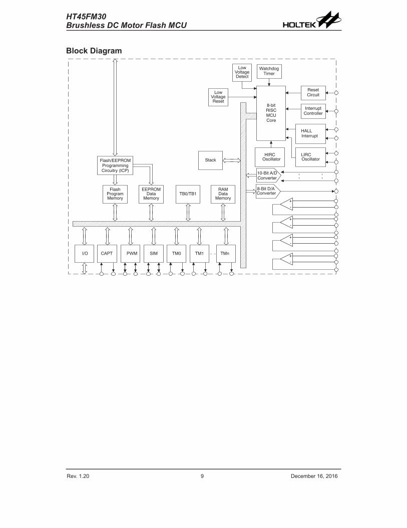
Block Diagram
Flash/EEPROMProgrammingCircuitry (ICP)
WatchdogTimer
8-bitRISCMCUCore
ResetCircuit
InterruptController
HALLInterrupt
10-Bit A/DConverter
Converter8-Bit D/A
LIRCOscillator
HIRCOscillatorStack
EEPROMData
Memory
FlashProgramMemory
RAMData
Memory
SIM TM0
LowVoltageReset
LowVoltageDetect
TM1 TMnPWM
+-
TB0/TB1
CAPTI/O
+-
+-
+-
Rev. 1.20 10 De�e��e� 1�� 201� Rev. 1.20 11 De�e��e� 1�� 201�
HT45FM30Brushless DC Motor Flash MCU
Pin Assignment
PA4/PWM1LPB5/PWM1HPB4/PWM0LPB3/PWM0H
PB2/INT0C/C0X/C3+PB1/INT0B/C1X/C3-
PB0/INT0A/C1-PA3/SCS/[PWM1H]/AN3/C1+ PA2/SCK/SCL/AN2/C0+/OPA+
PA1/TCK0/[TP1_1]/AN1/C0-PA0/TCK1/[INT2]/[TP1_0]/SDI/SDA/AN0/VREFVDDVSSPA7/[TCK0]/[INT1]/PCK/SDO/[PWM1H]PA6/INT1/TP0_1/TP1_1/[SDI/SDA]/[PWM2L]PA5/INT2/TP0_0/TP1_0/[SCK/SCL]/[PWM2H]
HT45FM30 16 TSSOP – A
PA4/PWM1LPB5/PWM1HPB4/PWM0LPB3/PWM0H
PA6/INT1/TP0_1/TP1_1/[SDI/SDA]/[PWM2L]PA5/INT2/TP0_0/TP1_0/[SCK/SCL]/[PWM2H]
PB2/INT0C/C0X/C3+
PC1/[TP0_1]/[SDO]/C2+PC0/[TP0_0]/[SDI/SDA]/C2-
PB1/INT0B/C1X/C3- PA0/[TCK1]/[INT2]/[TP1_0]/SDI/SDA/AN0/VREFVDDVSS
PA2/SCK/SCL/AN2/C0+/OPA+PA1/TCK0/[TP1_1]/AN1/C0-
PA7/[TCK0]/[INT1]/PCK/SDO/[PWM1H]
PC2/[SCK/SCL]/C2X/PWM2HPC3/[SCS]/C3X/PWM2L
PB0/INT0A/C1-PA3/SCS/[PWM1H]/AN3/C1+
HT45FM30 20 TSSOP – A
Rev. 1.20 10 De�e��e� 1�� 201� Rev. 1.20 11 De�e��e� 1�� 201�
HT45FM30Brushless DC Motor Flash MCU
Pin DescriptionPad Name Function OPT I/T O/T Description
PA0/TCK1/INT2/TP1_0/SDI/SDA/AN0/VREF
PA0 PAPUPAWU ST CMOS Bidi�e�tional I/O lines. Registe� ena�led pull-up
and wake-up.TCK1 ― ST — TM1 inputINT2 ― ST — Exte�nal Inte��upt 2 input
TP1_0 PRM0 ST CMOS TM1 I/OSDI — ST — SPI Data inputSDA — ST NMOS I2C DataAN0 ACERL AN — A/D �onve�te� input
VREF ADCR1 AN — A/D �onve�te� �efe�en�e input
PA1/TCK0/TP1_1/AN1/C0-
PA1 PAPUPAWU ST CMOS Bidi�e�tional I/O lines. Registe� ena�led pull-up
and wake-up.TCK0 PRM0 ST — TM0 inputTP1_1 PRM0 ST CMOS TM1 I/OAN1 ACERL AN — A/D �onve�te� inputC0- CP0C AN — Co�pa�ato� 0 negative input
PA2/SCK/SCL/AN2/C0+/OPA+
PA2 PAPUPAWU ST CMOS Bidi�e�tional I/O lines. Registe� ena�led pull-up
and wake-upSCK — ST CMOS SPI Se�ial Clo�kSCL — ST NMOS I2C Clo�kAN2 ACERL AN — A/D �onve�te� inputC0+ CP0C AN — Co�pa�ato� 0 positive input
OPA+ ADCR1 AN — OPA positive input
PA3/SCS/PWM1H/AN3/C1+
PA3 PAPUPAWU ST CMOS Bidi�e�tional I/O lines. Registe� ena�led pull-up
and wake-up.SCS — ST CMOS SPI Slave Sele�t
PWM1H PRM1PWMC1 — CMOS PWM output
AN3 ACERL AN — A/D �onve�te� inputC1+ CP1C AN — Co�pa�ato� 1 positive input
PA4/PWM1LPA4 PAPU
PAWU ST CMOS Bidi�e�tional I/O lines. Registe� ena�led pull-up and wake-up.
PWM1L PWMC1 — CMOS PWM output
PA5/INT2/TP0_0/TP1_0/SCK/SCL/PWM2H
PA5 PAPUPAWU ST CMOS Bidi�e�tional I/O lines. Registe� ena�led pull-up
and wake-up.INT2 — ST — Exte�nal Inte��upt 2 input
TP0_0 PRM0 ST CMOS TM0 I/OTP1_0 PRM0 ST CMOS TM1 I/OSCK — ST CMOS SPI Se�ial Clo�kSCL — ST NMOS I2C Clo�k
PWM2H PRM1PWMC1 — CMOS PWM output
Rev. 1.20 12 De�e��e� 1�� 201� Rev. 1.20 13 De�e��e� 1�� 201�
HT45FM30Brushless DC Motor Flash MCU
Pad Name Function OPT I/T O/T Description
PA�/INT1/TP0_1/TP1_1/SDI/SDA/PWM2L
PA� PAPUPAWU ST CMOS Bidi�e�tional I/O lines. Registe� ena�led pull-up
and wake-up.INT1 — ST — Exte�nal Inte��upt 1 input
TP0_1 PRM0 ST CMOS TM0 I/OTP1_1 PRM0 ST CMOS TM1 I/O
SDI — ST — SPI Data inputSDA — ST NMOS I2C Data
PWM2L PRM1PWMC1 — CMOS PWM output
PA7/TCK0/INT1/PCK/SDO/PWM1H
PA7 PAPUPAWU ST CMOS Bidi�e�tional I/O lines. Registe� ena�led pull-up
and wake-up.TCK0 PRM0 ST — TM0 inputINT1 — ST — Exte�nal Inte��upt 1 inputPCK — — CMOS Pe�iphe�al Clo�k outputSDO — — CMOS SPI Data output
PWM1H PRM1PWMC1 — CMOS PWM output
PB0/INT0A/C1-PB0 PBPU ST CMOS Bidi�e�tional I/O lines. Registe� ena�led pull-up.
INT0A — ST — Exte�nal Inte��upt 0 inputC1- CP1C AN — Co�pa�ato� 1 negative input
PB1/INT0B/C1X/C3-
PB1 PBPU ST CMOS Gene�al pu�pose I/O. Registe� ena�led pull-up.INT0B — ST — Exte�nal Inte��upt 0 inputC1X CP1C — CMOS Co�pa�ato� 1 outputC3- CP3C AN — Co�pa�ato� 3 negative input
PB2/INT0C/C0X/C3+
PB2 PBPU ST CMOS Bidi�e�tional I/O lines. Registe� ena�led pull-up.INT0C — ST — Exte�nal Inte��upt 0 inputC0X CP0C — CMOS Co�pa�ato� 0 outputC3+ CP3C AN — Co�pa�ato� 3 positive input
PB3/PWM0HPB3 PBPU ST CMOS Bidi�e�tional I/O lines. Registe� ena�led pull-up.
PWM0H — — CMOS PWM output
PB4/PWM0LPB4 PBPU ST CMOS Bidi�e�tional I/O lines. Registe� ena�led pull-up.
PWM0L — — CMOS PWM output
PB5/PWM1HPB5 PBPU ST CMOS Gene�al pu�pose I/O. Registe� ena�led pull-up .
PWM1H PRM1PWMC1 — CMOS PWM output
PC0/TP0_0/SDI/SDA/C2-
PC0 PCPU ST CMOS Gene�al pu�pose I/O. Registe� ena�led pull-up .TP0_0 PRM0 ST CMOS TM0 I/O
SDI — ST — SPI Data inputSDA — ST NMOS I2C DataC2- CP2C AN — Co�pa�ato� 2 negative input
PC1/TP0_1/SDO/C2+
PC1 PCPU ST CMOS Gene�al pu�pose I/O. Registe� ena�led pull-up .TP0_1 PRM0 ST CMOS TM0 I/OSDO — — CMOS SPI Data outputC2+ CP2C AN — Co�pa�ato� 2 positive input
Rev. 1.20 12 De�e��e� 1�� 201� Rev. 1.20 13 De�e��e� 1�� 201�
HT45FM30Brushless DC Motor Flash MCU
Pad Name Function OPT I/T O/T Description
PC2/SCK/SCL/C2X/PWM2H
PC2 PCPU ST CMOS Gene�al pu�pose I/O. Registe� ena�led pull-up SCK — ST CMOS SPI Se�ial Clo�kSCL — ST NMOS I2C Clo�kC2X CP2C — CMOS Co�pa�ato� 2 output
PWM2H PRM1PWMC1 — CMOS PWM output
PC3/SCS/C3X/PWM2L
PC3 PCPU ST CMOS Gene�al pu�pose I/O. Registe� ena�led pull-up .SCS — ST CMOS SPI Slave Sele�tC3X CP3C — CMOS Co�pa�ato� 3 output
PWM2L PRM1PWMC1 — CMOS PWM output
VDD VDD — PWR — Positive powe� supplyVSS VSS — PWR — Negative powe� supply� GND
Note:Thepinsinthetableareforthelargestpackagesize.Asaresultsomepinsonthesmallerpackagesmaynotexist.
I/T:Inputtype;O/T:Outputtype
OPT:Optionalbyregisteroption
PWR:Power;ST:SchmittTriggerinput
AN:Analoginputpin
CMOS:CMOSoutput
Absolute Maximum RatingsSupplyVoltage................................................................................................VSS-0.3VtoVSS+6.0VInputVoltage..................................................................................................VSS-0.3VtoVDD+0.3VStorageTemperature.................................................................................................. -50°Cto150°COperatingTemperature................................................................................................ -40°Cto85°CIOHTotal..................................................................................................................................-100mAIOLTotal................................................................................................................................... 100mATotalPowerDissipation........................................................................................................ 500mW
Note:Thesearestressratingsonly.Stressesexceeding therangespecifiedunder"AbsoluteMaximumRatings"maycausesubstantialdamagetothedevice.Functionaloperationofthisdeviceatotherconditionsbeyondthoselistedinthespecificationisnotimpliedandprolongedexposuretoextremeconditionsmayaffectdevicereliability.
Rev. 1.20 14 De�e��e� 1�� 201� Rev. 1.20 15 De�e��e� 1�� 201�
HT45FM30Brushless DC Motor Flash MCU
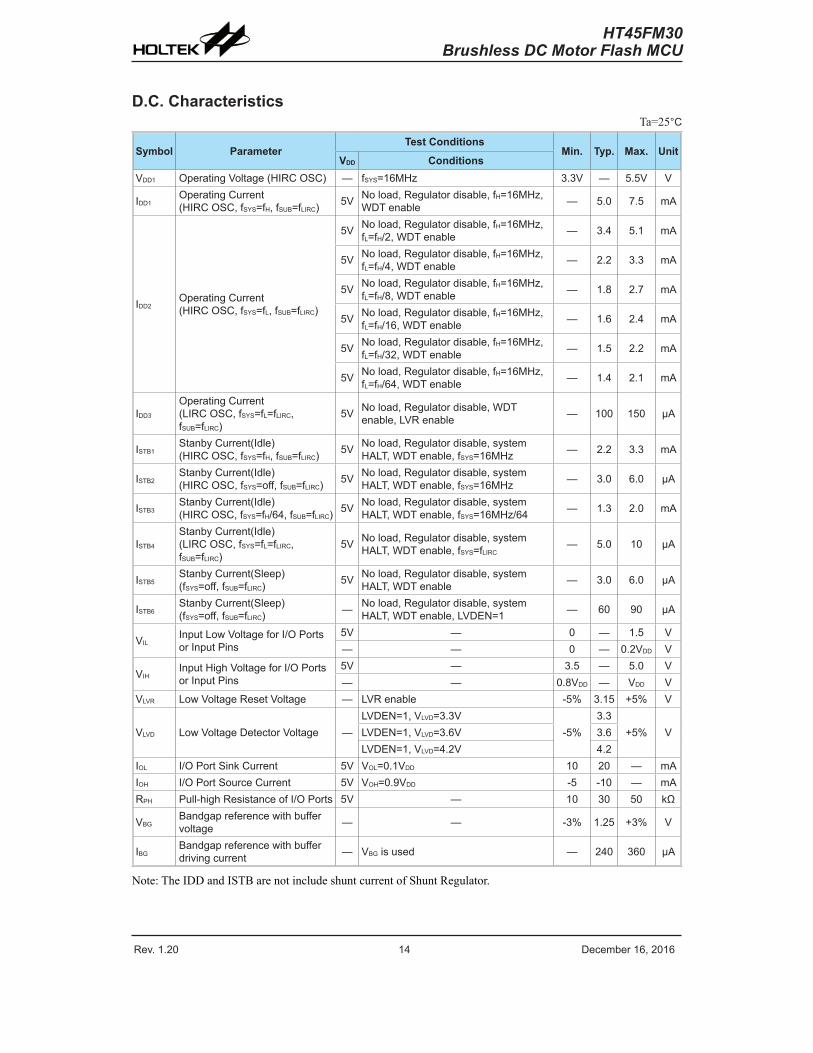
D.C. CharacteristicsTa=25°C
Symbol ParameterTest Conditions
Min. Typ. Max. UnitVDD Conditions
VDD1 Ope�ating Voltage (HIRC OSC) — fSYS=1�MHz 3.3V — 5.5V V
IDD1Ope�ating Cu��ent (HIRC OSC� fSYS=fH� fSUB=fLIRC) 5V No load� Regulato� disa�le� fH=1�MHz�
WDT ena�le — 5.0 7.5 �A
IDD2Ope�ating Cu��ent (HIRC OSC� fSYS=fL� fSUB=fLIRC)
5V No load� Regulato� disa�le� fH=1�MHz� fL=fH/2� WDT ena�le — 3.4 5.1 �A
5V No load� Regulato� disa�le� fH=1�MHz� fL=fH/4� WDT ena�le — 2.2 3.3 �A
5V No load� Regulato� disa�le� fH=1�MHz� fL=fH/8� WDT ena�le — 1.8 2.7 �A
5V No load� Regulato� disa�le� fH=1�MHz� fL=fH/1�� WDT ena�le — 1.� 2.4 �A
5V No load� Regulato� disa�le� fH=1�MHz� fL=fH/32� WDT ena�le — 1.5 2.2 �A
5V No load� Regulato� disa�le� fH=1�MHz� fL=fH/�4� WDT ena�le — 1.4 2.1 �A
IDD3
Ope�ating Cu��ent (LIRC OSC� fSYS=fL=fLIRC� fSUB=fLIRC)
5V No load� Regulato� disa�le� WDT ena�le� LVR ena�le — 100 150 μA
ISTB1Stan�y Cu��ent(Idle) (HIRC OSC� fSYS=fH� fSUB=fLIRC) 5V No load� Regulato� disa�le� syste�
HALT� WDT ena�le� fSYS=1�MHz — 2.2 3.3 �A
ISTB2Stan�y Cu��ent(Idle) (HIRC OSC� fSYS=off� fSUB=fLIRC) 5V No load� Regulato� disa�le� syste�
HALT� WDT ena�le� fSYS=1�MHz — 3.0 �.0 μA
ISTB3Stan�y Cu��ent(Idle) (HIRC OSC� fSYS=fH/�4� fSUB=fLIRC) 5V No load� Regulato� disa�le� syste�
HALT� WDT ena�le� fSYS=1�MHz/�4 — 1.3 2.0 �A
ISTB4
Stan�y Cu��ent(Idle) (LIRC OSC� fSYS=fL=fLIRC� fSUB=fLIRC)
5V No load� Regulato� disa�le� syste� HALT� WDT ena�le� fSYS=fLIRC
— 5.0 10 μA
ISTB5Stan�y Cu��ent(Sleep) (fSYS=off� fSUB=fLIRC) 5V No load� Regulato� disa�le� syste�
HALT� WDT ena�le — 3.0 �.0 μA
ISTB�Stan�y Cu��ent(Sleep) (fSYS=off� fSUB=fLIRC) — No load� Regulato� disa�le� syste�
HALT� WDT ena�le� LVDEN=1 — �0 90 μA
VILInput Low Voltage fo� I/O Po�ts o� Input Pins
5V — 0 — 1.5 V— — 0 — 0.2VDD V
VIHInput High Voltage fo� I/O Po�ts o� Input Pins
5V — 3.5 — 5.0 V— — 0.8VDD — VDD V
VLVR Low Voltage Reset Voltage — LVR ena�le -5% 3.15 +5% V
VLVD Low Voltage Dete�to� Voltage —LVDEN=1� VLVD=3.3V
-5%3.3
+5% VLVDEN=1� VLVD=3.�V 3.�LVDEN=1� VLVD=4.2V 4.2
IOL I/O Po�t Sink Cu��ent 5V VOL=0.1VDD 10 20 — �AIOH I/O Po�t Sou��e Cu��ent 5V VOH=0.9VDD -5 -10 — �ARPH Pull-high Resistan�e of I/O Po�ts 5V — 10 30 50 kΩ
VBGBandgap �efe�en�e with �uffe� voltage — — -3% 1.25 +3% V
IBGBandgap �efe�en�e with �uffe� d�iving �u��ent — VBG is used — 240 3�0 μA
Note:TheIDDandISTBarenotincludeshuntcurrentofShuntRegulator.
Rev. 1.20 14 De�e��e� 1�� 201� Rev. 1.20 15 De�e��e� 1�� 201�
HT45FM30Brushless DC Motor Flash MCU
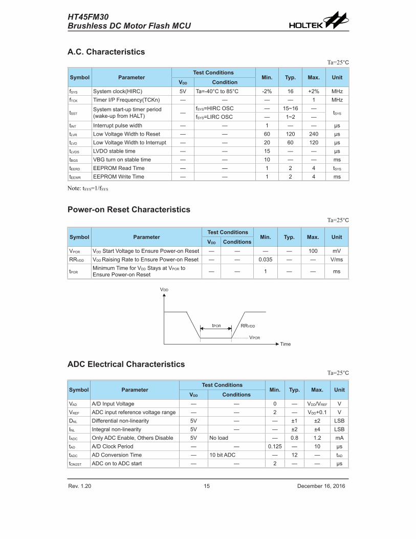
A.C. CharacteristicsTa=25°C
Symbol ParameterTest Conditions
Min. Typ. Max. UnitVDD Condition
fSYS Syste� �lo�k(HIRC) 5V Ta=-40°C to 85°C -2% 1� +2% MHzfTCK Ti�e� I/P F�equen�y(TCKn) — — — — 1 MHz
tSSTSyste� sta�t-up ti�e� pe�iod (wake-up f�o� HALT) —
fSYS=HIRC OSC — 15~1� —tSYS
fSYS=LIRC OSC — 1~2 —tINT Inte��upt pulse width — — 1 — — μstLVR Low Voltage Width to Reset — — �0 120 240 μstLVD Low Voltage Width to Inte��upt — — 20 �0 120 μstLVDS LVDO sta�le ti�e — — 15 — — μstBGS VBG tu�n on sta�le ti�e — — 10 — — �stEERD EEPROM Read Ti�e — — 1 2 4 tSYS
tEEWR EEPROM W�ite Ti�e — — 1 2 4 �s
Note:tSYS=1/fSYS
Power-on Reset CharacteristicsTa=25°C
Symbol ParameterTest Conditions
Min. Typ. Max. UnitVDD Conditions
VPOR VDD Sta�t Voltage to Ensu�e Powe�-on Reset — — — — 100 �VRRVDD VDD Raising Rate to Ensu�e Powe�-on Reset — — 0.035 — — V/�s
tPORMini�u� Ti�e fo� VDD Stays at VPOR to Ensu�e Powe�-on Reset — — 1 — — �s
� � � �
� � �
� � � �
� � � � �� � � �
ADC Electrical CharacteristicsTa=25°C
Symbol ParameterTest Conditions
Min. Typ. Max. UnitVDD Conditions
VAD A/D Input Voltage — — 0 — VDD/VREF VVREF ADC input �efe�en�e voltage �ange — — 2 — VDD+0.1 VDNL Diffe�ential non-linea�ity 5V — — ±1 ±2 LSBINL Integ�al non-linea�ity 5V — — ±2 ±4 LSBIADC Only ADC Ena�le� Othe�s Disa�le 5V No load — 0.8 1.2 �AtAD A/D Clo�k Pe�iod — — 0.125 — 10 μstADC AD Conve�sion Ti�e — 10 �it ADC — 12 — tAD
tON2ST ADC on to ADC sta�t — — 2 — — μs
Rev. 1.20 1� De�e��e� 1�� 201� Rev. 1.20 17 De�e��e� 1�� 201�
HT45FM30Brushless DC Motor Flash MCU
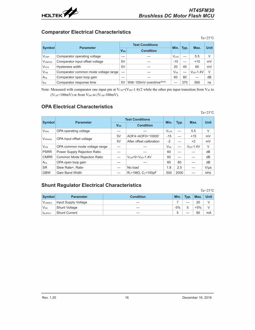
Comparator Electrical CharacteristicsTa=25°C
Symbol ParameterTest Conditions
Min. Typ. Max. UnitVDD Condition
VCMP Co�pa�ato� ope�ating voltage — — VLVR — 5.5 VVCMPOS Co�pa�ato� input offset voltage 5V — -10 — +10 �VVHYS Hyste�esis width 5V — 20 40 �0 �VVCM Co�pa�ato� �o��on �ode voltage �ange — — VSS — VDD-1.4V VAOL Co�pa�ato� open loop gain — — �0 80 — dBtPD Co�pa�ato� �esponse ti�e 5V With 100�V ove�d�ive(Note) — 370 5�0 ns
Note:MeasuredwithcomparatoroneinputpinatVCM=(VDD-1.4)/2whiletheotherpininputtransitionfromVSSto(VCM+100mV)orfromVDDto(VCM-100mV).
OPA Electrical CharacteristicsTa=25°C
Symbol ParameterTest Conditions
Min. Typ. Max. UnitVDD Condition
VOPA OPA ope�ating voltage — — VLVR — 5.5 V
VOPAOS OPA input offset voltage5V AOF4~AOF0=‘10000’ -15 — +15 �V5V Afte� offset �ali��ation -2 — +2 �V
VCM OPA �o��on �ode voltage �ange — — VSS — VDD-1.4V VPSRR Powe� Supply Reje�tion Ratio — — �0 — — dBCMRR Co��on Mode Reje�tion Ratio — VCM=0~VDD-1.4V �0 — — dBAOL OPA open loop gain — — �0 80 — dBSR Slew Rate+� Rate- — No load 1.8 2.5 — V/μsGBW Gain Band Width — RL=1MΩ, CL=100pF 500 2000 — kHz
Shunt Regulator Electrical CharacteristicsTa=25°C
Symbol Parameter Condition Min. Typ. Max. UnitVUNREG Input Supply Voltage — 7 — 20 VVDD Shunt Voltage — -5% 5 +5% VISUPPLY Shunt Cu��ent — 5 — 80 �A
Rev. 1.20 1� De�e��e� 1�� 201� Rev. 1.20 17 De�e��e� 1�� 201�
HT45FM30Brushless DC Motor Flash MCU
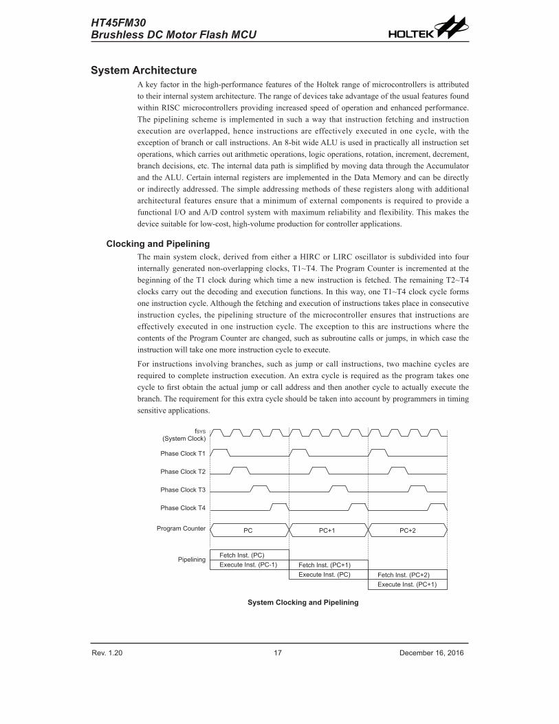
System ArchitectureAkeyfactorinthehigh-performancefeaturesoftheHoltekrangeofmicrocontrollersisattributedtotheirinternalsystemarchitecture.TherangeofdevicestakeadvantageoftheusualfeaturesfoundwithinRISCmicrocontrollersprovidingincreasedspeedofoperationandenhancedperformance.Thepipeliningscheme is implemented insuchaway that instruction fetchingand instructionexecutionareoverlapped,hence instructionsareeffectivelyexecuted inonecycle,with theexceptionofbranchorcallinstructions.An8-bitwideALUisusedinpracticallyallinstructionsetoperations,whichcarriesoutarithmeticoperations,logicoperations,rotation,increment,decrement,branchdecisions,etc.TheinternaldatapathissimplifiedbymovingdatathroughtheAccumulatorandtheALU.CertaininternalregistersareimplementedintheDataMemoryandcanbedirectlyor indirectlyaddressed.Thesimpleaddressingmethodsof theseregistersalongwithadditionalarchitectural featuresensure thataminimumofexternalcomponents is required toprovideafunctionalI/OandA/Dcontrolsystemwithmaximumreliabilityandflexibility.Thismakes thedevicesuitableforlow-cost,high-volumeproductionforcontrollerapplications.
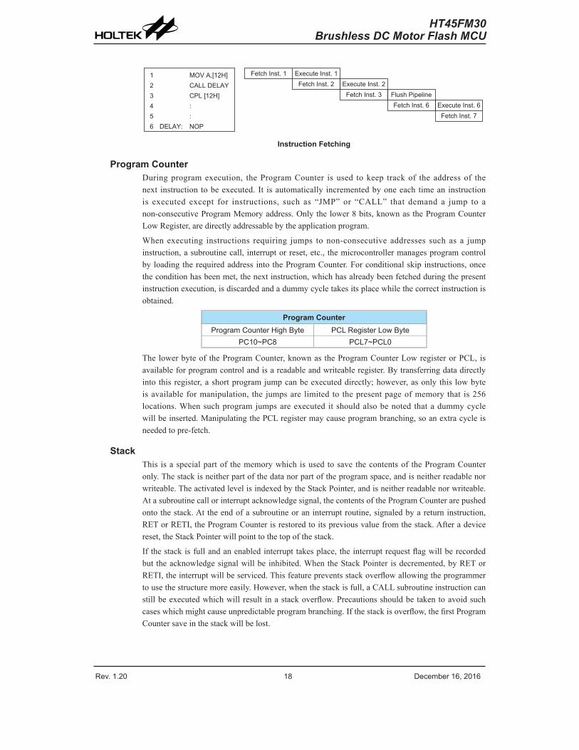
Clocking and PipeliningThemainsystemclock,derivedfromeitheraHIRCorLIRCoscillator issubdivided intofourinternallygeneratednon-overlappingclocks,T1~T4.TheProgramCounter is incrementedat thebeginningoftheT1clockduringwhichtimeanewinstructionisfetched.TheremainingT2~T4clockscarryoutthedecodingandexecutionfunctions.Inthisway,oneT1~T4clockcycleformsoneinstructioncycle.Althoughthefetchingandexecutionofinstructionstakesplaceinconsecutiveinstructioncycles, thepipeliningstructureof themicrocontrollerensures that instructionsareeffectivelyexecuted inone instructioncycle.Theexception to thisare instructionswhere thecontentsoftheProgramCounterarechanged,suchassubroutinecallsorjumps,inwhichcasetheinstructionwilltakeonemoreinstructioncycletoexecute.
For instructions involvingbranches,suchas jumporcall instructions, twomachinecyclesarerequired tocomplete instructionexecution.Anextracycle is requiredas theprogramtakesonecycletofirstobtaintheactualjumporcalladdressandthenanothercycletoactuallyexecutethebranch.Therequirementforthisextracycleshouldbetakenintoaccountbyprogrammersintimingsensitiveapplications.
� � � � � � � � � � � � � � � �� � � � � � � � � � � � � � � � � � � � � � � � � � � � � � � � � � � �
� � � � � � � � � � � � � � � � � � � � � � � � � � � � � � � � � � � �� � � � � � � � � � � � � � � � � � �
� � � � � � � � �
� � � � � � � � � � � � � �
� � � � � � � � � � � � �
� � � � � � � � � � � � � � �
� � � � � � � � � � � � � �
� � � � � � � � � � � � � �
� � � � � � � � � � � � � �
� � � � � � � � � �
System Clocking and Pipelining
Rev. 1.20 18 De�e��e� 1�� 201� Rev. 1.20 19 De�e��e� 1�� 201�
HT45FM30Brushless DC Motor Flash MCU
� � � � � � � � � � � � � � � � � � � � � � � � � � � �� � � � � � � � � � � � �
� � � � � � � � � � � � �
���� � � � � � �
� � � � � � � � � � �� � � � � � � � � �� � � � � � � � ���� � �
� � � � � � � � � � � � � � �� � � � � � � � � � � � �
� � � � � � � � � � � � � � � � � � � � � � � � � � � � � � � � � � � � � �
Instruction Fetching
Program CounterDuringprogramexecution, theProgramCounter isused tokeep trackof theaddressof thenext instruction tobeexecuted. It isautomatically incrementedbyoneeach timean instructionis executed except for instructions, such as “JMP” or “CALL” that demand a jump to anon-consecutiveProgramMemoryaddress.Onlythelower8bits,knownastheProgramCounterLowRegister,aredirectlyaddressablebytheapplicationprogram.
Whenexecuting instructions requiring jumps tonon-consecutiveaddresses suchas a jumpinstruction,asubroutinecall, interruptorreset,etc., themicrocontrollermanagesprogramcontrolbyloadingtherequiredaddressintotheProgramCounter.Forconditionalskipinstructions,oncetheconditionhasbeenmet,thenextinstruction,whichhasalreadybeenfetchedduringthepresentinstructionexecution,isdiscardedandadummycycletakesitsplacewhilethecorrectinstructionisobtained.
Program CounterP�og�a� Counte� High Byte PCL Registe� Low Byte
PC10~PC8 PCL7~PCL0
Thelowerbyteof theProgramCounter,knownastheProgramCounterLowregisterorPCL,isavailableforprogramcontrolandisareadableandwriteableregister.Bytransferringdatadirectlyintothisregister,ashortprogramjumpcanbeexecuteddirectly;however,asonlythis lowbyteisavailable formanipulation, the jumpsare limited to thepresentpageofmemory that is256locations.Whensuchprogramjumpsareexecuted itshouldalsobenoted thatadummycyclewillbeinserted.ManipulatingthePCLregistermaycauseprogrambranching,soanextracycleisneededtopre-fetch.
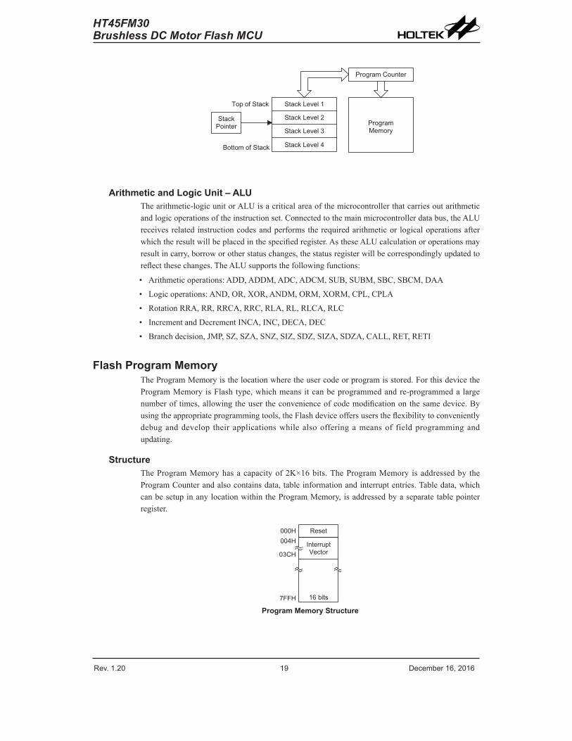
StackThis isaspecialpartof thememorywhichisusedtosavethecontentsof theProgramCounteronly.Thestackisneitherpartofthedatanorpartoftheprogramspace,andisneitherreadablenorwriteable.TheactivatedlevelisindexedbytheStackPointer,andisneitherreadablenorwriteable.Atasubroutinecallorinterruptacknowledgesignal,thecontentsoftheProgramCounterarepushedontothestack.Attheendofasubroutineoraninterruptroutine,signaledbyareturninstruction,RETorRETI,theProgramCounterisrestoredtoitspreviousvaluefromthestack.Afteradevicereset,theStackPointerwillpointtothetopofthestack.
Ifthestackisfullandanenabledinterrupttakesplace,theinterruptrequestflagwillberecordedbuttheacknowledgesignalwillbeinhibited.WhentheStackPointer isdecremented,byRETorRETI,theinterruptwillbeserviced.Thisfeaturepreventsstackoverflowallowingtheprogrammertousethestructuremoreeasily.However,whenthestackisfull,aCALLsubroutineinstructioncanstillbeexecutedwhichwillresult inastackoverflow.Precautionsshouldbetakentoavoidsuchcaseswhichmightcauseunpredictableprogrambranching.Ifthestackisoverflow,thefirstProgramCountersaveinthestackwillbelost.
Rev. 1.20 18 De�e��e� 1�� 201� Rev. 1.20 19 De�e��e� 1�� 201�
HT45FM30Brushless DC Motor Flash MCU
� � � � � � � � � � � � � � �
� � � � � � � � � � � �
� � � � � � � � � � � � �
� � � � � � � � � � � � �
� � � � � � � � � � � �
� � � � � � � � � � � �
� � � � � � � � � � � �
� � � � �� � � � � � �
� � � � � � � � � � � � � � �
Arithmetic and Logic Unit – ALUThearithmetic-logicunitorALUisacriticalareaofthemicrocontrollerthatcarriesoutarithmeticandlogicoperationsoftheinstructionset.Connectedtothemainmicrocontrollerdatabus,theALUreceivesrelatedinstructioncodesandperformstherequiredarithmeticor logicaloperationsafterwhichtheresultwillbeplacedinthespecifiedregister.AstheseALUcalculationoroperationsmayresultincarry,borroworotherstatuschanges,thestatusregisterwillbecorrespondinglyupdatedtoreflectthesechanges.TheALUsupportsthefollowingfunctions:
• Arithmeticoperations:ADD,ADDM,ADC,ADCM,SUB,SUBM,SBC,SBCM,DAA
• Logicoperations:AND,OR,XOR,ANDM,ORM,XORM,CPL,CPLA
• RotationRRA,RR,RRCA,RRC,RLA,RL,RLCA,RLC
• IncrementandDecrementINCA,INC,DECA,DEC
• Branchdecision,JMP,SZ,SZA,SNZ,SIZ,SDZ,SIZA,SDZA,CALL,RET,RETI
Flash Program MemoryTheProgramMemoryisthelocationwheretheusercodeorprogramisstored.ForthisdevicetheProgramMemoryisFlashtype,whichmeansitcanbeprogrammedandre-programmeda largenumberoftimes,allowingtheusertheconvenienceofcodemodificationonthesamedevice.Byusingtheappropriateprogrammingtools,theFlashdeviceoffersuserstheflexibilitytoconvenientlydebuganddevelop their applicationswhilealsoofferingameansof fieldprogrammingandupdating.
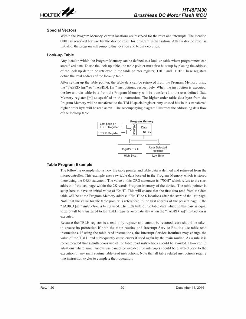
StructureTheProgramMemoryhasacapacityof2K×16bits.TheProgramMemoryisaddressedby theProgramCounterandalsocontainsdata,tableinformationandinterruptentries.Tabledata,whichcanbesetupinanylocationwithintheProgramMemory,isaddressedbyaseparatetablepointerregister.
� � � �
� � � �� � � � � � � � �� � � � � �
� � � � � � �
� � � � � � � � �
Program Memory Structure
Rev. 1.20 20 De�e��e� 1�� 201� Rev. 1.20 21 De�e��e� 1�� 201�
HT45FM30Brushless DC Motor Flash MCU
Special VectorsWithintheProgramMemory,certainlocationsarereservedfortheresetandinterrupts.Thelocation000His reserved foruseby thedevice reset forprograminitialisation.Afteradevice reset isinitiated,theprogramwilljumptothislocationandbeginexecution.
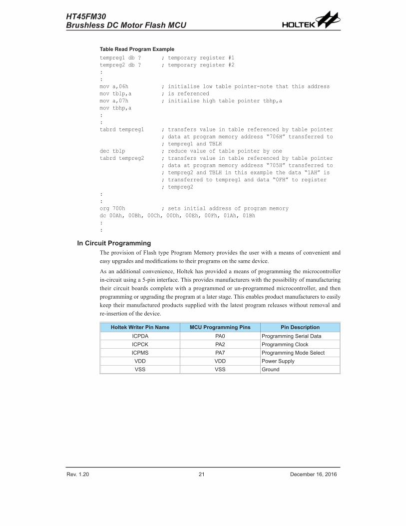
Look-up TableAnylocationwithintheProgramMemorycanbedefinedasalook-uptablewhereprogrammerscanstorefixeddata.Tousethelook-uptable,thetablepointermustfirstbesetupbyplacingtheaddressof thelookupdatatoberetrievedinthetablepointerregister,TBLPandTBHP.Theseregistersdefinethetotaladdressofthelook-uptable.
Aftersettingupthetablepointer,thetabledatacanberetrievedfromtheProgramMemoryusingthe“TABRD[m]”or“TABRDL[m]”instructions,respectively.Whentheinstructionisexecuted,thelowerordertablebytefromtheProgramMemorywillbetransferredtotheuserdefinedDataMemoryregister [m]asspecified in the instruction.Thehigherorder tabledatabyte fromtheProgramMemorywillbetransferredtotheTBLHspecialregister.Anyunusedbitsinthistransferredhigherorderbytewillbereadas“0”.Theaccompanyingdiagramillustratestheaddressingdataflowofthelook-uptable.
� � � � � � � � � � � � � � � � � � � � � � � � � �� � � � � � � �
� � � � � � � � � � � � � � �
� � � � � � � � � � � �
� � �
������� � � � � � � �
� � � � � � � � � � � � � �� � � � � � � � � � � �� � � � � � � � � � � �
Table Program ExampleThefollowingexampleshowshowthetablepointerandtabledataisdefinedandretrievedfromthemicrocontroller.ThisexampleusesrawtabledatalocatedintheProgramMemorywhichisstoredthereusingtheORGstatement.ThevalueatthisORGstatementis“700H”whichreferstothestartaddressofthelastpagewithinthe2KwordsProgramMemoryofthedevice.Thetablepointerissetupheretohaveaninitialvalueof“06H”.ThiswillensurethatthefirstdatareadfromthedatatablewillbeattheProgramMemoryaddress“706H”or6locationsafterthestartofthelastpage.Notethatthevalueforthetablepointerisreferencedtothefirstaddressofthepresentpageifthe“TABRD[m]”instructionisbeingused.ThehighbyteofthetabledatawhichinthiscaseisequaltozerowillbetransferredtotheTBLHregisterautomaticallywhenthe“TABRD[m]”instructionisexecuted.
Because theTBLHregister isaread-onlyregisterandcannotberestored,careshouldbe takentoensure itsprotection ifboth themain routineand InterruptServiceRoutineuse table readinstructions. Ifusing the tableread instructions, theInterruptServiceRoutinesmaychange thevalueoftheTBLHandsubsequentlycauseerrorsifusedagainbythemainroutine.Asaruleitisrecommendedthatsimultaneoususeofthetablereadinstructionsshouldbeavoided.However, insituationswheresimultaneoususecannotbeavoided,theinterruptsshouldbedisabledpriortotheexecutionofanymainroutinetable-readinstructions.Notethatalltablerelatedinstructionsrequiretwoinstructioncyclestocompletetheiroperation.
Rev. 1.20 20 De�e��e� 1�� 201� Rev. 1.20 21 De�e��e� 1�� 201�
HT45FM30Brushless DC Motor Flash MCU
Table Read Program Exampletempreg1 db ? ; temporary register #1tempreg2 db ? ; temporary register #2::mov a,06h ; initialise low table pointer-note that this addressmov tblp,a ; is referencedmov a,07h ; initialise high table pointer tbhp,amov tbhp,a::tabrd tempreg1 ; transfers value in table referenced by table pointer ; data at program memory address “706H” transferred to ; tempreg1 and TBLHdec tblp ; reduce value of table pointer by onetabrd tempreg2 ; transfers value in table referenced by table pointer ; data at program memory address “705H” transferred to ; tempreg2 and TBLH in this example the data “1AH” is ; transferred to tempreg1 and data “0FH” to register ; tempreg2::org 700h ; sets initial address of program memorydc 00Ah, 00Bh, 00Ch, 00Dh, 00Eh, 00Fh, 01Ah, 01Bh::
In Circuit ProgrammingTheprovisionofFlashtypeProgramMemoryprovides theuserwithameansofconvenientandeasyupgradesandmodificationstotheirprogramsonthesamedevice.
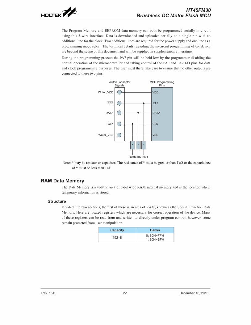
Asanadditionalconvenience,Holtekhasprovidedameansofprogrammingthemicrocontrollerin-circuitusinga5-pininterface.Thisprovidesmanufacturerswiththepossibilityofmanufacturingtheircircuitboardscompletewithaprogrammedorun-programmedmicrocontroller,and thenprogrammingorupgradingtheprogramatalaterstage.Thisenablesproductmanufacturerstoeasilykeeptheirmanufacturedproductssuppliedwiththelatestprogramreleaseswithoutremovalandre-insertionofthedevice.
Holtek Writer Pin Name MCU Programming Pins Pin DescriptionICPDA PA0 P�og�a��ing Se�ial DataICPCK PA2 P�og�a��ing Clo�kICPMS PA7 P�og�a��ing Mode Sele�tVDD VDD Powe� SupplyVSS VSS G�ound
Rev. 1.20 22 De�e��e� 1�� 201� Rev. 1.20 23 De�e��e� 1�� 201�
HT45FM30Brushless DC Motor Flash MCU
TheProgramMemoryandEEPROMdatamemorycanbothbeprogrammedserially in-circuitusing this5-wire interface.Data isdownloadedanduploadedseriallyonasinglepinwithanadditionallinefortheclock.Twoadditionallinesarerequiredforthepowersupplyandonelineasaprogrammingmodeselect.Thetechnicaldetailsregardingthein-circuitprogrammingofthedevicearebeyondthescopeofthisdocumentandwillbesuppliedinsupplemenetaryliterature.
Duringtheprogrammingprocess thePA7pinwillbeheld lowbytheprogrammerdisablingthenormaloperationof themicrocontrollerandtakingcontrolof thePA0andPA2I/Opinsfordataandclockprogrammingpurposes.Theusermusttheretakecaretoensurethatnootheroutputsareconnectedtothesetwopins.
� � �
� � � � � � � � � �
� � �
� � � �
� � �
� � � � � � � � � �
� � � � � � � � � � � � �
� � � �
� � �
� � �
� �
� � �
� � � � � � � � � � � � � � �� � � � � � �
� � � � � � � � � � � � � � � �
Note:*mayberesistororcapacitor.Theresistanceof*mustbegreaterthan1kΩorthecapacitanceof*mustbelessthan1nF.
RAM Data MemoryTheDataMemoryisavolatileareaof8-bitwideRAMinternalmemoryandisthelocationwheretemporaryinformationisstored.
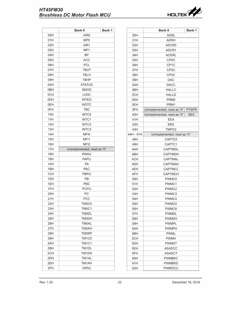
StructureDividedintotwosections,thefirstoftheseisanareaofRAM,knownastheSpecialFunctionDataMemory.Herearelocatedregisterswhicharenecessaryforcorrectoperationofthedevice.Manyoftheseregisterscanbereadfromandwrittentodirectlyunderprogramcontrol,however,someremainprotectedfromusermanipulation.
Capacity Banks
192×8 0: 80H~FFH 1: 80H~BFH
Rev. 1.20 22 De�e��e� 1�� 201� Rev. 1.20 23 De�e��e� 1�� 201�
HT45FM30Brushless DC Motor Flash MCU
Bank 0 Bank 100H IAR001H MP002H IAR103H MP104H BP05H ACC0�H PCL07H TBLP08H TBLH09H TBHP0AH STATUS0BH SMOD0CH LVDC0DH INTEG0EH WDTC0FH TBC10H INTC011H INTC112H INTC213H INTC314H MFI015H MFI11�H MFI217H Uni�ple�ented� �ead as “0”18H PAWU19H PAPU1AH PA1BH PAC1CH PBPU1DH PB1EH PBC1FH PCPU20H PC21H PCC22H TM0C023H TM0C124H TM0DL25H TM0DH2�H TM0AL27H TM0AH28H TM0RP29H TM1C02AH TM1C12BH TM1DL2CH TM1DH2DH TM1AL2EH TM1AH2FH OPAC
Bank 0 Bank 130H ADRL31H ADRH32H ADCR033H ADCR134H ACERL35H CP0C3�H CP1C37H CP2C38H CP3C39H DAC3AH DACC3BH HALLC3CH HALLD3DH PRM03EH PRM13FH Uni�ple�ented� �ead as “0” PTSFR40H Uni�ple�ented� �ead as “0” EEC41H EEA42H EED43H TMPC0
44H - 47H Uni�ple�ented� �ead as “0”48H CAPTC049H CAPTC14AH CAPTMDL4BH CAPTMDH4CH CAPTMAL4DH CAPTMAH4EH CAPTMCL4FH CAPTMCH50H PWMC051H PWMC152H PWMC253H PWMC354H PWMC455H PWMC55�H PWMC�57H PWMDL58H PWMDH59H PWMPL5AH PWMPH5BH PWML5CH PWMH5DH PWMDT5EH ASADCC5FH ASADCT�0H PWMBKC�1H PWMBKD�2H PWMOCC
Rev. 1.20 24 De�e��e� 1�� 201� Rev. 1.20 25 De�e��e� 1�� 201�
HT45FM30Brushless DC Motor Flash MCU
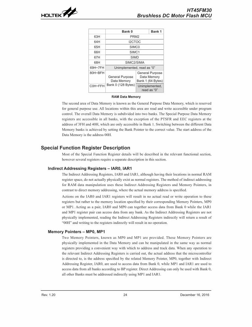
Bank 0 Bank 1�3H PRM2�4H I2CTOC�5H SIMC0��H SIMC1�7H SIMD�8H SIMC2/SIMA
�9H~7FH Uni�ple�ented� �ead as “0”80H~BFH
Gene�al Pu�pose Data Me�o�y
Bank 0 (128 Bytes)
Gene�al Pu�pose Data Me�o�y
Bank 1 (�4 Bytes)C0H~FFH Uni�ple�ented�
�ead as “0”
RAM Data Memory
ThesecondareaofDataMemoryisknownastheGeneralPurposeDataMemory,whichisreservedforgeneralpurposeuse.Alllocationswithinthisareaarereadandwriteaccessibleunderprogramcontrol.TheoverallDataMemoryissubdividedintotwobanks.TheSpecialPurposeDataMemoryregistersareaccessible inallbanks,with theexceptionof thePTSFRandEECregistersat theaddressof3FHand40H,whichareonlyaccessibleinBank1.SwitchingbetweenthedifferentDataMemorybanksisachievedbysettingtheBankPointertothecorrectvalue.ThestartaddressoftheDataMemoryistheaddress00H.
Special Function Register DescriptionMostoftheSpecialFunctionRegisterdetailswillbedescribedintherelevantfunctionalsection,howeverseveralregistersrequireaseparatedescriptioninthissection.
Indirect Addressing Registers – IAR0, IAR1TheIndirectAddressingRegisters,IAR0andIAR1,althoughhavingtheirlocationsinnormalRAMregisterspace,donotactuallyphysicallyexistasnormalregisters.ThemethodofindirectaddressingforRAMdatamanipulationuses theseIndirectAddressingRegistersandMemoryPointers, incontrasttodirectmemoryaddressing,wheretheactualmemoryaddressisspecified.
ActionsontheIAR0andIAR1registerswill result innoactualreadorwriteoperationto theseregistersbutrathertothememorylocationspecifiedbytheircorrespondingMemoryPointers,MP0orMP1.Actingasapair, IAR0andMP0cantogetheraccessdatafromBank0while theIAR1andMP1registerpaircanaccessdatafromanybank.AstheIndirectAddressingRegistersarenotphysicallyimplemented,readingtheIndirectAddressingRegistersindirectlywillreturnaresultof“00H”andwritingtotheregistersindirectlywillresultinnooperation.
Memory Pointers – MP0, MP1TwoMemoryPointers, knownasMP0andMP1areprovided.TheseMemoryPointers arephysicallyimplementedintheDataMemoryandcanbemanipulatedinthesamewayasnormalregistersprovidingaconvenientwaywithwhichtoaddressandtrackdata.WhenanyoperationtotherelevantIndirectAddressingRegistersiscarriedout,theactualaddressthatthemicrocontrollerisdirectedto,istheaddressspecifiedbytherelatedMemoryPointer,MP0,togetherwithIndirectAddressingRegister,IAR0,areusedtoaccessdatafromBank0,whileMP1andIAR1areusedtoaccessdatafromallbanksaccordingtoBPregister.DirectAddressingcanonlybeusedwithBank0,allotherBanksmustbeaddressedindirectlyusingMP1andIAR1.
Rev. 1.20 24 De�e��e� 1�� 201� Rev. 1.20 25 De�e��e� 1�� 201�
HT45FM30Brushless DC Motor Flash MCU
ThefollowingexampleshowshowtoclearasectionoffourDataMemorylocationsalreadydefinedaslocationsadres1toadres4.
Indirect Addressing Program Exampledata .section ´data´adres1 db ?adres2 db ?adres3 db ?adres4 db ?block db ?code.section at 0 ´code´org00hstart: mov a, 04h ; setup size of block mov block, a mova,offsetadres1 ;AccumulatorloadedwithfirstRAMaddress movmp0,a ;setupmemorypointerwithfirstRAMaddressloop: clrIAR0 ;clearthedataataddressdefinedbymp0 inc mp0 ; increment memory pointer sdz block ; check if last memory location has been cleared jmp loopcontinue:
Theimportantpointtonotehereisthatintheexampleshownabove,noreferenceismadetospecificDataMemoryaddresses.
Bank Pointer – BPForthisdevice,theDataMemoryisdividedintotwobanks.SelectingtherequiredDataMemoryareaisachievedusingtheBankPointer.Bit0oftheBankPointerisusedtoselectDataMemoryBanks0~1.TheDataMemoryisinitialisedtoBank0afterareset,exceptforaWDTtime-outresetinthePowerDownMode,inwhichcase,theDataMemorybankremainsunaffected.ItshouldbenotedthattheSpecialFunctionDataMemoryisnotaffectedbythebankselection,whichmeansthattheSpecialFunctionRegisterscanbeaccessedfromwithinanybank.DirectlyaddressingtheDataMemorywillalwaysresultinBank0beingaccessedirrespectiveofthevalueoftheBankPointer.AccessingdatafrombanksotherthanBank0mustbeimplementedusingIndirectaddressing.AsboththeProgramMemoryandDataMemorysharethesameBankPointerRegister,caremustbetakenduringprogramming.
BP Register
Bit 7 6 5 4 3 2 1 0Na�e — — — — — — — DMBP0R/W — — — — — — — R/WPOR — — — — — — — 0
Bit7~1 Unimplemented,readas“0”Bit0 DMBP0:SelectDataMemoryBanks
0:Bank01:Bank1
Rev. 1.20 2� De�e��e� 1�� 201� Rev. 1.20 27 De�e��e� 1�� 201�
HT45FM30Brushless DC Motor Flash MCU
Accumulator – ACCTheAccumulator iscentral to theoperationofanymicrocontrollerand isclosely relatedwithoperationscarriedoutby theALU.TheAccumulator is theplacewhereall intermediateresultsfromtheALUarestored.Without theAccumulator itwouldbenecessary towrite theresultofeachcalculationorlogicaloperationsuchasaddition,subtraction,shift,etc., totheDataMemoryresultinginhigherprogrammingandtimingoverheads.Data transferoperationsusually involvethetemporarystoragefunctionoftheAccumulator;forexample,whentransferringdatabetweenoneuserdefinedregisterandanother, it isnecessary todo thisbypassingthedata throughtheAccumulatorasnodirecttransferbetweentworegistersispermitted.
Program Counter Low Register – PCLToprovideadditionalprogramcontrolfunctions, the lowbyteof theProgramCounter ismadeaccessibletoprogrammersbylocatingitwithintheSpecialPurposeareaoftheDataMemory.Bymanipulatingthisregister,directjumpstootherprogramlocationsareeasilyimplemented.LoadingavaluedirectlyintothisPCLregisterwillcauseajumptothespecifiedProgramMemorylocation,however,astheregisterisonly8-bitwide,onlyjumpswithinthecurrentProgramMemorypagearepermitted.Whensuchoperationsareused,notethatadummycyclewillbeinserted.
Look-up Table Registers – TBLP, TBHP, TBLHThesethreespecialfunctionregistersareusedtocontroloperationof thelook-uptablewhichisstoredintheProgramMemory.TBLPandTBHParethetablepointerandindicates thelocationwhere the tabledata is located.Theirvaluemustbesetupbeforeany tablereadcommandsareexecuted.Theirvaluecanbechanged,forexampleusingthe“INC”or“DEC”instructions,allowingforeasytabledatapointingandreading.TBLHisthelocationwherethehighorderbyteofthetabledataisstoredafteratablereaddatainstructionhasbeenexecuted.Notethatthelowerordertabledatabyteistransferredtoauserdefinedlocation.
Status Register – STATUSThis8-bit registercontains thezeroflag(Z),carryflag(C),auxiliarycarryflag(AC),overflowflag(OV),powerdownflag(PDF),andwatchdogtime-outflag(TO).Thesearithmetic/logicaloperation and systemmanagement flags areused to record the status andoperationof themicrocontroller.WiththeexceptionoftheTOandPDFflags,bitsinthestatusregistercanbealteredbyinstructionslikemostotherregisters.AnydatawrittenintothestatusregisterwillnotchangetheTOorPDFflag.Inaddition,operationsrelatedtothestatusregistermaygivedifferentresultsduetothedifferentinstructionoperations.TheTOflagcanbeaffectedonlybyasystempower-up,aWDTtime-outorbyexecutingthe“CLRWDT”or“HALT”instruction.ThePDFflagisaffectedonlybyexecutingthe“HALT”or“CLRWDT”instructionorduringasystempower-up.TheZ,OV,ACandCflagsgenerallyreflectthestatusofthelatestoperations.• Cissetifanoperationresultsinacarryduringanadditionoperationorifaborrowdoesnottakeplaceduringasubtractionoperation;otherwiseCiscleared.Cisalsoaffectedbyarotatethroughcarryinstruction.
• ACissetifanoperationresultsinacarryoutofthelownibblesinaddition,ornoborrowfromthehighnibbleintothelownibbleinsubtraction;otherwiseACiscleared.
• Zissetiftheresultofanarithmeticorlogicaloperationiszero;otherwiseZiscleared.• OVisset ifanoperationresults inacarryintothehighest-orderbitbutnotacarryoutof thehighest-orderbit,orviceversa;otherwiseOViscleared.
• PDFisclearedbyasystempower-uporexecutingthe“CLRWDT”instruction.PDFissetbyexecutingthe“HALT”instruction.
• TOisclearedbyasystempower-uporexecutingthe“CLRWDT”or“HALT”instruction.TOissetbyaWDTtime-out.
Rev. 1.20 2� De�e��e� 1�� 201� Rev. 1.20 27 De�e��e� 1�� 201�
HT45FM30Brushless DC Motor Flash MCU
Inaddition,onenteringaninterruptsequenceorexecutingasubroutinecall,thestatusregisterwillnotbepushedontothestackautomatically.Ifthecontentsofthestatusregistersareimportantandifthesubroutinecancorruptthestatusregister,precautionsmustbetakentocorrectlysaveit.
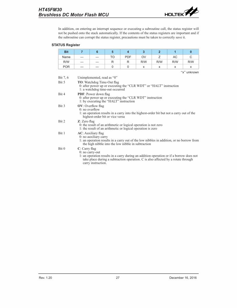
STATUS Register
Bit 7 6 5 4 3 2 1 0Na�e — — TO PDF OV Z AC CR/W — — R R R/W R/W R/W R/WPOR — — 0 0 x x x x
“x” unknown
Bit7,6 Unimplemented,readas“0”Bit5 TO:WatchdogTime-Outflag
0:afterpoweruporexecutingthe“CLRWDT”or“HALT”instruction1:awatchdogtime-outoccurred
Bit4 PDF:Powerdownflag0:afterpoweruporexecutingthe“CLRWDT”instruction1:byexecutingthe“HALT”instruction
Bit3 OV:Overflowflag0:nooverflow1:anoperationresultsinacarryintothehighest-orderbitbutnotacarryoutofthehighest-orderbitorviceversa
Bit2 Z:Zeroflag0:theresultofanarithmeticorlogicaloperationisnotzero1:theresultofanarithmeticorlogicaloperationiszero
Bit1 AC:Auxiliaryflag0:noauxiliarycarry1:anoperationresultsinacarryoutofthelownibblesinaddition,ornoborrowfromthehighnibbleintothelownibbleinsubtraction
Bit0 C:Carryflag0:nocarry-out1:anoperationresultsinacarryduringanadditionoperationorifaborrowdoesnottakeplaceduringasubtractionoperation.Cisalsoaffectedbyarotatethroughcarryinstruction.
Rev. 1.20 28 De�e��e� 1�� 201� Rev. 1.20 29 De�e��e� 1�� 201�
HT45FM30Brushless DC Motor Flash MCU
EEPROM Data MemoryOneofthespecialfeaturesinthedeviceisitsinternalEEPROMDataMemory.EEPROM,whichstandsforElectricallyErasableProgrammableReadOnlyMemory,isbyitsnatureanon-volatileformofmemory,withdataretentionevenwhenitspowersupply is removed.Byincorporatingthiskindofdatamemory,awholenewhostofapplicationpossibilitiesaremadeavailabletothedesigner.TheavailabilityofEEPROMstorageallowsinformationsuchasproduct identificationnumbers,calibrationvalues,specificuserdata,systemsetupdataorotherproductinformationtobestoreddirectlywithintheproductmicrocontroller.
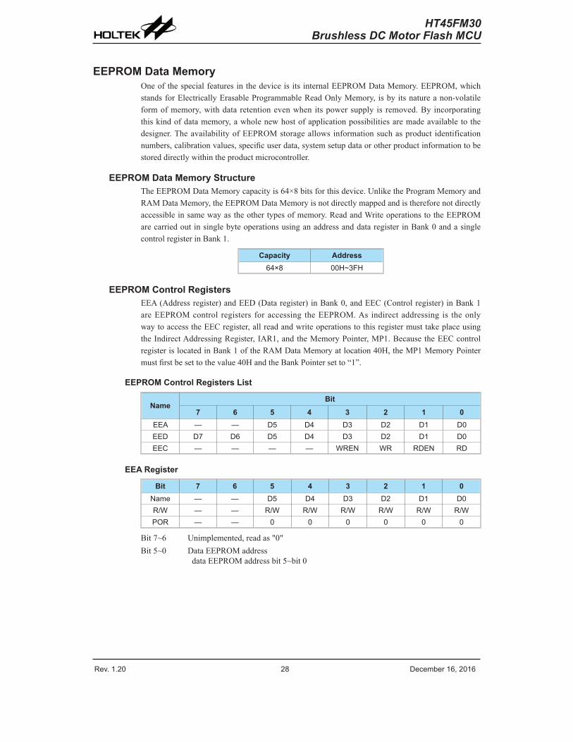
EEPROM Data Memory StructureTheEEPROMDataMemorycapacityis64×8bitsforthisdevice.UnliketheProgramMemoryandRAMDataMemory,theEEPROMDataMemoryisnotdirectlymappedandisthereforenotdirectlyaccessibleinsamewayastheothertypesofmemory.ReadandWriteoperationstotheEEPROMarecarriedoutinsinglebyteoperationsusinganaddressanddataregisterinBank0andasinglecontrolregisterinBank1.
Capacity Address�4×8 00H~3FH
EEPROM Control RegistersEEA(Addressregister)andEED(Dataregister)inBank0,andEEC(Controlregister)inBank1areEEPROMcontrol registers foraccessing theEEPROM.As indirectaddressing is theonlywaytoaccesstheEECregister,allreadandwriteoperationstothisregistermusttakeplaceusingtheIndirectAddressingRegister,IAR1,andtheMemoryPointer,MP1.BecausetheEECcontrolregisterislocatedinBank1oftheRAMDataMemoryatlocation40H,theMP1MemoryPointermustfirstbesettothevalue40HandtheBankPointersetto“1”.
EEPROM Control Registers List
NameBit
7 6 5 4 3 2 1 0EEA — — D5 D4 D3 D2 D1 D0EED D7 D� D5 D4 D3 D2 D1 D0EEC — — — — WREN WR RDEN RD
EEA Register
Bit 7 6 5 4 3 2 1 0Na�e — — D5 D4 D3 D2 D1 D0R/W — — R/W R/W R/W R/W R/W R/WPOR — — 0 0 0 0 0 0
Bit7~6 Unimplemented,readas"0"Bit5~0 DataEEPROMaddress
dataEEPROMaddressbit5~bit0
Rev. 1.20 28 De�e��e� 1�� 201� Rev. 1.20 29 De�e��e� 1�� 201�
HT45FM30Brushless DC Motor Flash MCU
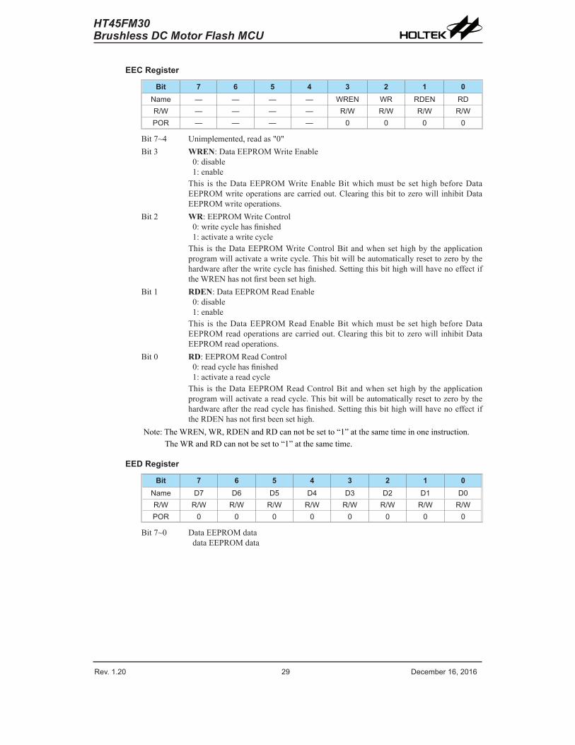
EEC Register
Bit 7 6 5 4 3 2 1 0Na�e — — — — WREN WR RDEN RDR/W — — — — R/W R/W R/W R/WPOR — — — — 0 0 0 0
Bit7~4 Unimplemented,readas"0"Bit3 WREN:DataEEPROMWriteEnable
0:disable1:enableThis is theDataEEPROMWriteEnableBitwhichmustbesethighbeforeDataEEPROMwriteoperationsarecarriedout.Clearingthisbit tozerowill inhibitDataEEPROMwriteoperations.
Bit2 WR:EEPROMWriteControl0:writecyclehasfinished1:activateawritecycleThis is theDataEEPROMWriteControlBitandwhensethighbytheapplicationprogramwillactivateawritecycle.Thisbitwillbeautomaticallyresettozerobythehardwareafterthewritecyclehasfinished.SettingthisbithighwillhavenoeffectiftheWRENhasnotfirstbeensethigh.
Bit1 RDEN:DataEEPROMReadEnable0:disable1:enableThis is theDataEEPROMReadEnableBitwhichmustbesethighbeforeDataEEPROMreadoperationsarecarriedout.Clearingthisbit tozerowill inhibitDataEEPROMreadoperations.
Bit0 RD:EEPROMReadControl0:readcyclehasfinished1:activateareadcycleThis is theDataEEPROMReadControlBitandwhensethighbytheapplicationprogramwillactivateareadcycle.Thisbitwillbeautomaticallyresettozerobythehardwareafterthereadcyclehasfinished.SettingthisbithighwillhavenoeffectiftheRDENhasnotfirstbeensethigh.
Note:TheWREN,WR,RDENandRDcannotbesetto“1”atthesametimeinoneinstruction.TheWRandRDcannotbesetto“1”atthesametime.
EED Register
Bit 7 6 5 4 3 2 1 0Na�e D7 D� D5 D4 D3 D2 D1 D0R/W R/W R/W R/W R/W R/W R/W R/W R/WPOR 0 0 0 0 0 0 0 0
Bit7~0 DataEEPROMdatadataEEPROMdata
Rev. 1.20 30 De�e��e� 1�� 201� Rev. 1.20 31 De�e��e� 1�� 201�
HT45FM30Brushless DC Motor Flash MCU
Reading Data from the EEPROMToreaddatafromtheEEPROM,thereadenablebit,RDEN,intheEECregistermustfirstbesethightoenablethereadfunction.TheEEPROMaddressofthedatatobereadmustthenbeplacedintheEEAregister.IftheRDbitintheEECregisterisnowsethigh,areadcyclewillbeinitiated.SettingtheRDbithighwillnotinitiateareadoperationif theRDENbithasnotbeenset.Whenthereadcycleterminates,theRDbitwillbeautomaticallyclearedtozero,afterwhichthedatacanbereadfromtheEEDregister.ThedatawillremainintheEEDregisteruntilanotherreadorwriteoperationisexecuted.TheapplicationprogramcanpolltheRDbittodeterminewhenthedataisvalidforreading.
Writing Data to the EEPROMTheEEPROMaddressofthedatatobewrittenmustfirstbeplacedintheEEAregisterandthedataplacedintheEEDregister.TowritedatatotheEEPROM,thewriteenablebit,WREN,intheEECregistermustfirstbesethightoenablethewritefunction.Afterthis,theWRbitintheEECregistermustbe immediatelysethighto initiateawritecycle.Thesetwoinstructionsmustbeexecutedconsecutively.Theglobal interruptbitEMIshouldalsofirstbeclearedbeforeimplementinganywriteoperations,andthensetagainafterthewritecyclehasstarted.NotethatsettingtheWRbithighwillnotinitiateawritecycleiftheWRENbithasnotbeenset.AstheEEPROMwritecycleiscontrolledusinganinternaltimerwhoseoperationisasynchronoustomicrocontrollersystemclock,acertaintimewillelapsebeforethedatawillhavebeenwrittenintotheEEPROM.DetectingwhenthewritecyclehasfinishedcanbeimplementedeitherbypollingtheWRbitintheEECregisterorbyusingtheEEPROMinterrupt.Whenthewritecycleterminates,theWRbitwillbeautomaticallycleared tozeroby themicrocontroller, informing theuser that thedatahasbeenwritten to theEEPROM.TheapplicationprogramcanthereforepolltheWRbittodeterminewhenthewritecyclehasended.
Write ProtectionProtectionagainst inadvertentwriteoperation isprovided inseveralways.After thedevice ispowered-on theWriteEnablebit in thecontrol registerwillbeclearedpreventinganywriteoperations.Alsoatpower-ontheBankPointer,BP,willbereset tozero,whichmeansthatDataMemoryBank0willbeselected.AstheEEPROMcontrolregisterislocatedinBank1,thisaddsafurthermeasureofprotectionagainstspuriouswriteoperations.Duringnormalprogramoperation,ensuringthattheWriteEnablebitinthecontrolregisterisclearedwillsafeguardagainstincorrectwriteoperations.
EEPROM InterruptTheEEPROMwrite interrupt is generatedwhen anEEPROMwrite cycle has ended.TheEEPROMinterruptmustfirstbeenabledbysettingtheDEEbit intherelevantinterruptregister.Howeveras theEEPROMiscontainedwithinaMulti-functionInterrupt, theassociatedmulti-function interruptenablebitmustalsobeset.WhenanEEPROMwritecycleends, theDEFrequestflaganditsassociatedmulti-functioninterruptrequestflagwillbothbeset.If theglobal,EEPROMandMulti-function interrupts are enabledand the stack isnot full, a jump to theassociatedMulti-function Interruptvectorwill takeplace.When the interrupt isservicedonlytheMulti-functioninterruptflagwillbeautomaticallyreset, theEEPROMinterruptflagmustbemanuallyresetbytheapplicationprogram.MoredetailscanbeobtainedintheInterruptsection.
Rev. 1.20 30 De�e��e� 1�� 201� Rev. 1.20 31 De�e��e� 1�� 201�
HT45FM30Brushless DC Motor Flash MCU
Programming ConsiderationsCaremustbe taken thatdata isnot inadvertentlywritten to theEEPROM.ProtectioncanbeenhancedbyensuringthattheWriteEnablebitisnormallyclearedtozerowhennotwriting.AlsotheBankPointercouldbenormallyclearedtozeroasthiswouldinhibitaccesstoBank1wheretheEEPROMcontrolregisterexist.Althoughcertainlynotnecessary,considerationmightbegivenintheapplicationprogramtothecheckingofthevalidityofnewwritedatabyasimplereadbackprocess.
WhenwritingdatatheWRbitmustbesethighimmediatelyaftertheWRENbithasbeensethigh,toensurethewritecycleexecutescorrectly.Theglobal interruptbitEMIshouldalsobeclearedbeforeawritecycleisexecutedandthenre-enabledafterthewritecyclestarts.
Programming Examples
Reading data from the EEPROM – polling methodMOVA,EEPROM_ADRES ;userdefinedaddressMOVEEA,AMOVA,040H ;setupmemorypointerMP1MOVMP1,A ;MP1pointstoEECregisterMOVA,01H ;setupBankPointerMOVBP,ASETIAR1.1 ;setRDENbit,enablereadoperationsSETIAR1.0 ;startReadCycle–setRDbitBACK:SZIAR1.0 ;checkforreadcycleendJMPBACKCLRIAR1 ;disableEEPROMread/writeCLRBPMOVA,EED ;movereaddatatoregisterMOVREAD_DATA,A
Writing Data to the EEPROM – polling methodMOVA,EEPROM_ADRES ;userdefinedaddressMOVEEA,AMOVA,EEPROM_DATA ;userdefineddataMOVEED,AMOVA,040H ;setupmemorypointerMP1MOVMP1,A ;MP1pointstoEECregisterMOVA,01H ;setupBankPointerMOVBP,ASETIAR1.3 ;setWRENbit,enablewriteoperationsSETIAR1.2 ;startWriteCycle–setWRbitBACK:SZIAR1.2 ;checkforwritecycleendJMPBACKCLRIAR1 ;disableEEPROMread/writeCLRBP
Rev. 1.20 32 De�e��e� 1�� 201� Rev. 1.20 33 De�e��e� 1�� 201�
HT45FM30Brushless DC Motor Flash MCU
OscillatorVariousoscillatoroptionsoffer theuserawide rangeof functionsaccording to theirvariousapplication requirements.The flexible featuresof theoscillator functionsensure that thebestoptimisationcanbeachievedintermsofspeedandpowersaving.Oscillatorselectionsandoperationareselectedthroughregisters.
System Oscillator OverviewInadditiontobeingthesourceofthemainsystemclocktheoscillatorsalsoprovideclocksourcesfor theWatchdogTimerandTimeBasefunctions.Thedeviceprovidestwooscillatorcircuitsforsystemclocks,named thehighfrequency internalRCoscillator,HIRC,and the lowfrequencyinternal32kHzRCoscillator,LIRC.
Type Name Freq.Inte�nal High Speed RC HIRC 1�MHzInte�nal Low Speed RC LIRC 32kHz
Oscillator Types
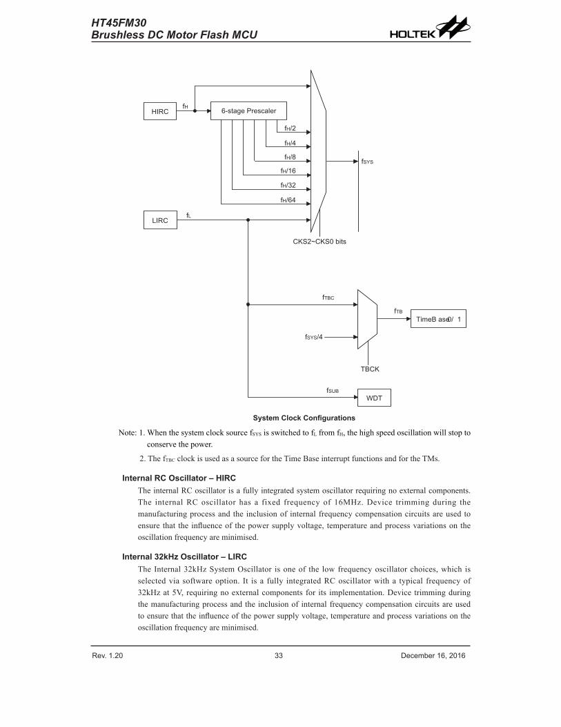
System Clock ConfigurationsThedevicehastwodifferentclocksourcesforboththeCPUandperipheralfunctionoperation.Byprovidingtheusertwoclockoptionsandregisterprogramming,aclocksystemcanbeconfiguredtoobtainmaximumapplicationperformance.Themainsystemclock,cancomefromeitherahighfrequency,fH,orlowfrequency,fL,andisselectedusingtheHLCLKbitandCKS2~CKS0bitsintheSMODregister.ThehighspeedsystemclockcanbesourcedfromanHIRCoscillator.ThelowspeedsystemclocksourcecanbesourcedfromtheinternalclockfL,sourcedfromLIRCoscillator.
Theotherchoice,which isadividedversionof thehighspeedsystemoscillatorhasarangeoffH/2~fH/64.Thereare twoadditional internalclocks for theperipheral circuits, the substituteclock,fSUB,andtheTimeBaseclock,fTBC.EachoftheseinternalclocksissourcedfromtheLIRCoscillator.
Rev. 1.20 32 De�e��e� 1�� 201� Rev. 1.20 33 De�e��e� 1�� 201�
HT45FM30Brushless DC Motor Flash MCU
� � � �
� � � �
� �
� � � � �
� � � � �
� � � � �
� � � �
� � � �
� � � �
� � � � � � � � � � �
� �
� � � � � � � � � � � � � �
� � � �
� � � � � �
� � � �
� � �
� � � � � � � � � � �� � �
� � � �
� � � �
System Clock Configurations
Note:1.WhenthesystemclocksourcefSYSisswitchedtofLfromfH,thehighspeedoscillationwillstoptoconservethepower.
2.ThefTBCclockisusedasasourcefortheTimeBaseinterruptfunctionsandfortheTMs.
Internal RC Oscillator – HIRCTheinternalRCoscillatorisafullyintegratedsystemoscillatorrequiringnoexternalcomponents.The internalRCoscillator has a fixed frequencyof 16MHz.Device trimmingduring themanufacturingprocessandtheinclusionof internalfrequencycompensationcircuitsareusedtoensurethat theinfluenceof thepowersupplyvoltage, temperatureandprocessvariationsontheoscillationfrequencyareminimised.
Internal 32kHz Oscillator – LIRCTheInternal32kHzSystemOscillator isoneof the lowfrequencyoscillatorchoices,which isselectedviasoftwareoption. It isa fully integratedRCoscillatorwitha typical frequencyof32kHzat5V,requiringnoexternalcomponentsfor its implementation.Device trimmingduringthemanufacturingprocessandtheinclusionofinternalfrequencycompensationcircuitsareusedtoensurethattheinfluenceofthepowersupplyvoltage,temperatureandprocessvariationsontheoscillationfrequencyareminimised.
Rev. 1.20 34 De�e��e� 1�� 201� Rev. 1.20 35 De�e��e� 1�� 201�
HT45FM30Brushless DC Motor Flash MCU
Operating ModesPresentdayapplicationsrequirethat theirmicrocontrollershavehighperformancebutoftenstilldemandthattheyconsumeaslittlepoweraspossible,conflictingrequirementsthatareespeciallytrueinbatterypoweredportableapplications.Thefastclocksrequiredforhighperformancewillbytheirnatureincreasecurrentconsumptionandofcoursevice-verse, lowerspeedclocksreducecurrentconsumption.AsHoltekhasprovidedthedevicewithbothhighandlowspeedclocksourcesandthemeanstoswitchbetweenthemdynamically, theusercanoptimisetheoperationof theirmicrocontrollertoachievethebestperformance/powerratio.
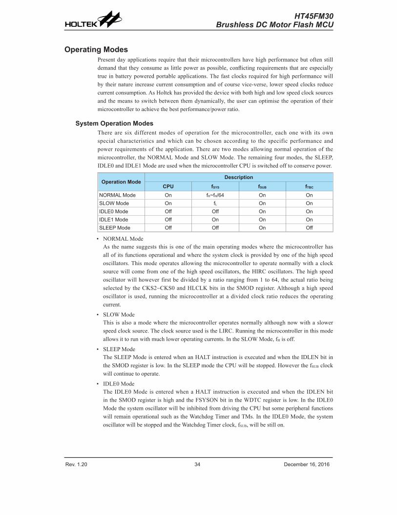
System Operation ModesThere are six differentmodesof operation for themicrocontroller, eachonewith its ownspecial characteristics andwhichcanbe chosenaccording to the specificperformanceandpowerrequirementsof theapplication.Thereare twomodesallowingnormaloperationof themicrocontroller, theNORMALModeandSLOWMode.Theremainingfourmodes, theSLEEP,IDLE0andIDLE1ModeareusedwhenthemicrocontrollerCPUisswitchedofftoconservepower.
Operation ModeDescription
CPU fSYS fSUB fTBC
NORMAL Mode On fH~fH/�4 On OnSLOW Mode On fL On OnIDLE0 Mode Off Off On OnIDLE1 Mode Off On On OnSLEEP Mode Off Off On Off
• NORMALModeAsthenamesuggests this isoneof themainoperatingmodeswhere themicrocontrollerhasallofitsfunctionsoperationalandwherethesystemclockisprovidedbyoneofthehighspeedoscillators.Thismodeoperatesallowingthemicrocontroller tooperatenormallywithaclocksourcewillcomefromoneof thehighspeedoscillators, theHIRCoscillators.Thehighspeedoscillatorwillhoweverfirstbedividedbyaratiorangingfrom1to64, theactualratiobeingselectedby theCKS2~CKS0andHLCLKbits in theSMODregister.Althoughahighspeedoscillator isused, running themicrocontrolleratadividedclockratio reduces theoperatingcurrent.
• SLOWModeThis isalsoamodewhere themicrocontrolleroperatesnormallyalthoughnowwithaslowerspeedclocksource.TheclocksourceusedistheLIRC.Runningthemicrocontrollerinthismodeallowsittorunwithmuchloweroperatingcurrents.IntheSLOWMode,fHisoff.
• SLEEPModeTheSLEEPModeisenteredwhenanHALTinstructionisexecutedandwhentheIDLENbitintheSMODregisterislow.IntheSLEEPmodetheCPUwillbestopped.HoweverthefSUBclockwillcontinuetooperate.
• IDLE0ModeTheIDLE0Mode isenteredwhenaHALTinstruction isexecutedandwhen the IDLENbitintheSMODregisterishighandtheFSYSONbit intheWDTCregisteris low.IntheIDLE0ModethesystemoscillatorwillbeinhibitedfromdrivingtheCPUbutsomeperipheralfunctionswillremainoperationalsuchastheWatchdogTimerandTMs.IntheIDLE0Mode,thesystemoscillatorwillbestoppedandtheWatchdogTimerclock,fSUB,willbestillon.
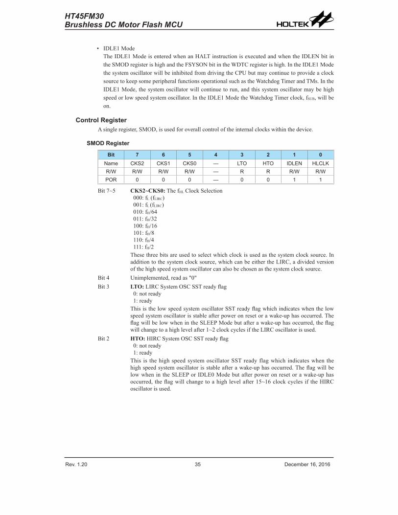
Rev. 1.20 34 De�e��e� 1�� 201� Rev. 1.20 35 De�e��e� 1�� 201�
HT45FM30Brushless DC Motor Flash MCU
• IDLE1ModeTheIDLE1ModeisenteredwhenanHALTinstructionisexecutedandwhentheIDLENbitintheSMODregisterishighandtheFSYSONbitintheWDTCregisterishigh.IntheIDLE1ModethesystemoscillatorwillbeinhibitedfromdrivingtheCPUbutmaycontinuetoprovideaclocksourcetokeepsomeperipheralfunctionsoperationalsuchastheWatchdogTimerandTMs.IntheIDLE1Mode,thesystemoscillatorwillcontinuetorun,andthissystemoscillatormaybehighspeedorlowspeedsystemoscillator.IntheIDLE1ModetheWatchdogTimerclock,fSUB,willbeon.
Control RegisterAsingleregister,SMOD,isusedforoverallcontroloftheinternalclockswithinthedevice.
SMOD Register
Bit 7 6 5 4 3 2 1 0Na�e CKS2 CKS1 CKS0 — LTO HTO IDLEN HLCLKR/W R/W R/W R/W — R R R/W R/WPOR 0 0 0 — 0 0 1 1
Bit7~5 CKS2~CKS0:ThefHLClockSelection000:fL(fLIRC)001:fL(fLIRC)010:fH/64011:fH/32100:fH/16101:fH/8110:fH/4111:fH/2Thesethreebitsareusedtoselectwhichclockisusedasthesystemclocksource.Inadditiontothesystemclocksource,whichcanbeeithertheLIRC,adividedversionofthehighspeedsystemoscillatorcanalsobechosenasthesystemclocksource.
Bit4 Unimplemented,readas"0"Bit3 LTO:LIRCSystemOSCSSTreadyflag
0:notready1:readyThisisthelowspeedsystemoscillatorSSTreadyflagwhichindicateswhenthelowspeedsystemoscillatorisstableafterpoweronresetorawake-uphasoccurred.TheflagwillbelowwhenintheSLEEPModebutafterawake-uphasoccurred,theflagwillchangetoahighlevelafter1~2clockcyclesiftheLIRCoscillatorisused.
Bit2 HTO:HIRCSystemOSCSSTreadyflag0:notready1:readyThis is thehighspeedsystemoscillatorSSTreadyflagwhich indicateswhen thehighspeedsystemoscillatorisstableafterawake-uphasoccurred.TheflagwillbelowwhenintheSLEEPorIDLE0Modebutafterpoweronresetorawake-uphasoccurred, theflagwillchangetoahighlevelafter15~16clockcycles if theHIRCoscillatorisused.
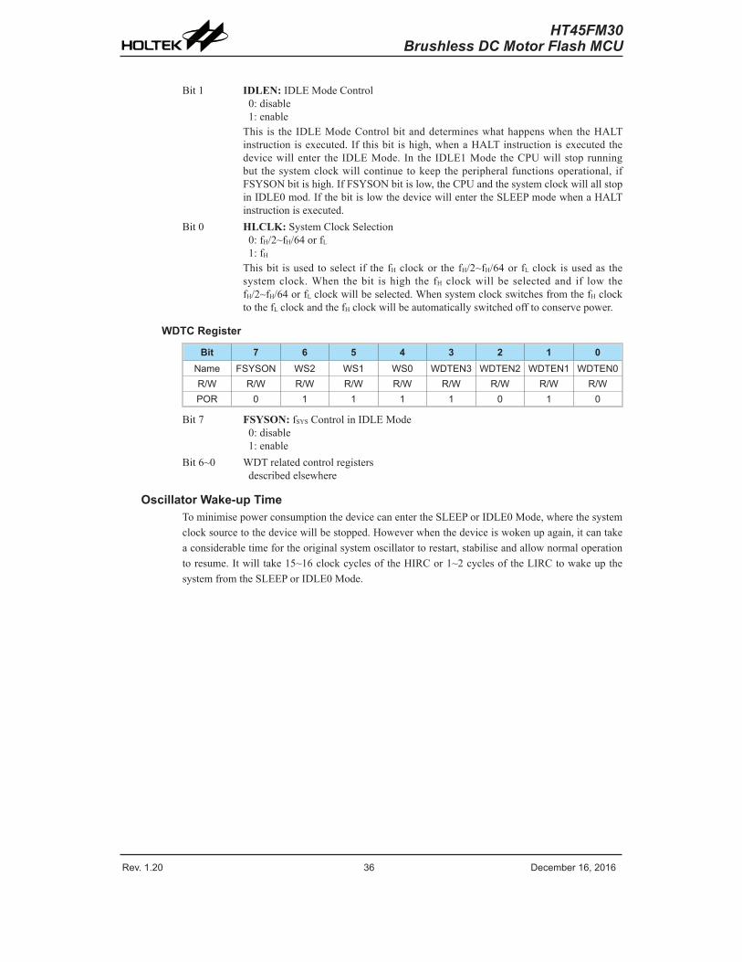
Rev. 1.20 3� De�e��e� 1�� 201� Rev. 1.20 37 De�e��e� 1�� 201�
HT45FM30Brushless DC Motor Flash MCU
Bit1 IDLEN:IDLEModeControl0:disable1:enableThis is theIDLEModeControlbitanddetermineswhathappenswhentheHALTinstructionisexecuted.If thisbit ishigh,whenaHALTinstructionisexecutedthedevicewillenter theIDLEMode. In theIDLE1Mode theCPUwillstoprunningbut thesystemclockwillcontinue tokeep theperipheral functionsoperational, ifFSYSONbitishigh.IfFSYSONbitislow,theCPUandthesystemclockwillallstopinIDLE0mod.IfthebitislowthedevicewillentertheSLEEPmodewhenaHALTinstructionisexecuted.
Bit0 HLCLK:SystemClockSelection0:fH/2~fH/64orfL1:fH
Thisbit isusedtoselect if thefHclockor thefH/2~fH/64orfLclockisusedas thesystemclock.When thebit ishigh the fH clockwillbe selectedand if low thefH/2~fH/64orfLclockwillbeselected.WhensystemclockswitchesfromthefHclocktothefLclockandthefHclockwillbeautomaticallyswitchedofftoconservepower.
WDTC Register
Bit 7 6 5 4 3 2 1 0Na�e FSYSON WS2 WS1 WS0 WDTEN3 WDTEN2 WDTEN1 WDTEN0R/W R/W R/W R/W R/W R/W R/W R/W R/WPOR 0 1 1 1 1 0 1 0
Bit7 FSYSON:fSYSControlinIDLEMode0:disable1:enable
Bit6~0 WDTrelatedcontrolregistersdescribedelsewhere
Oscillator Wake-up TimeTominimisepowerconsumptionthedevicecanentertheSLEEPorIDLE0Mode,wherethesystemclocksourcetothedevicewillbestopped.Howeverwhenthedeviceiswokenupagain,itcantakeaconsiderabletimefortheoriginalsystemoscillatortorestart,stabiliseandallownormaloperationtoresume.Itwilltake15~16clockcyclesoftheHIRCor1~2cyclesoftheLIRCtowakeupthesystemfromtheSLEEPorIDLE0Mode.
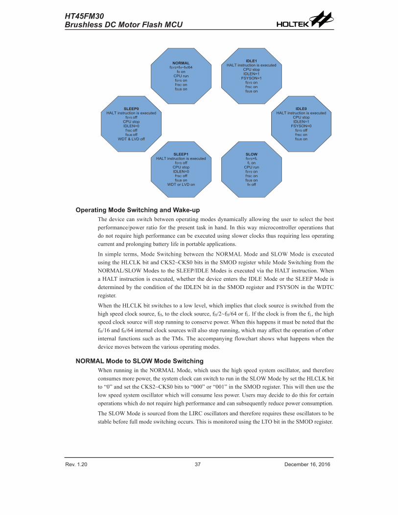
Rev. 1.20 3� De�e��e� 1�� 201� Rev. 1.20 37 De�e��e� 1�� 201�
HT45FM30Brushless DC Motor Flash MCU
� � � � � �� � � � � � � � � � � � � � � � � � � � � � � � � � � �
� � � � � � �� � � � � � � � � � � � �� � � � � � � �� � � � � � �
� � � � � � � � � � � � �
� � � � � �� � � � � � � � � � � �
� � � � �� � � � � �� � � � � �� � � � � � �� � � � � �
� � � � �� � � � � � � � � � � � � � � � � � � � � � � � � � � �
� � � � � � � � � � � �
� � � � � � � � � � �� � � � � � �� � � � � � �
� � � � �� � � � � � � � � � � � � � � � � � � � � � � � � � � �
� � � � � � � � � � � �
� � � � � �� � � � � � �� � � � � � �� � � � � �
� � � �� � � � � �� � � � �
� � � � � �� � � � � �� � � � � � �� � � � � �� � � � � �
� � � � � �� � � � � � � � � � � � � � � � � � � � � � � � � � � �
� � � � � � �� � � � � � � � � � � � �� � � � � � � �� � � � � �
� � � � � � � � � � � � �
Operating Mode Switching and Wake-upThedevicecanswitchbetweenoperatingmodesdynamicallyallowingtheusertoselect thebestperformance/powerratiofor thepresent taskinhand.Inthiswaymicrocontrolleroperationsthatdonotrequirehighperformancecanbeexecutedusingslowerclocksthusrequiringlessoperatingcurrentandprolongingbatterylifeinportableapplications.
Insimple terms,ModeSwitchingbetween theNORMALModeandSLOWMode isexecutedusingtheHLCLKbitandCKS2~CKS0bitsintheSMODregisterwhileModeSwitchingfromtheNORMAL/SLOWModestotheSLEEP/IDLEModesisexecutedviatheHALTinstruction.WhenaHALTinstructionisexecuted,whetherthedeviceenterstheIDLEModeortheSLEEPModeisdeterminedbytheconditionoftheIDLENbitintheSMODregisterandFSYSONintheWDTCregister.
WhentheHLCLKbitswitchestoalowlevel,whichimpliesthatclocksourceisswitchedfromthehighspeedclocksource,fH,totheclocksource,fH/2~fH/64orfL.IftheclockisfromthefL,thehighspeedclocksourcewillstoprunningtoconservepower.WhenthishappensitmustbenotedthatthefH/16andfH/64internalclocksourceswillalsostoprunning,whichmayaffecttheoperationofotherinternalfunctionssuchas theTMs.Theaccompanyingflowchartshowswhathappenswhenthedevicemovesbetweenthevariousoperatingmodes.
NORMAL Mode to SLOW Mode SwitchingWhenrunningintheNORMALMode,whichusesthehighspeedsystemoscillator,andthereforeconsumesmorepower,thesystemclockcanswitchtorunintheSLOWModebysettheHLCLKbitto“0”andsettheCKS2~CKS0bitsto“000”or“001”intheSMODregister.Thiswillthenusethelowspeedsystemoscillatorwhichwillconsumelesspower.Usersmaydecidetodothisforcertainoperationswhichdonotrequirehighperformanceandcansubsequentlyreducepowerconsumption.
TheSLOWModeissourcedfromtheLIRCoscillatorsandthereforerequirestheseoscillatorstobestablebeforefullmodeswitchingoccurs.ThisismonitoredusingtheLTObitintheSMODregister.
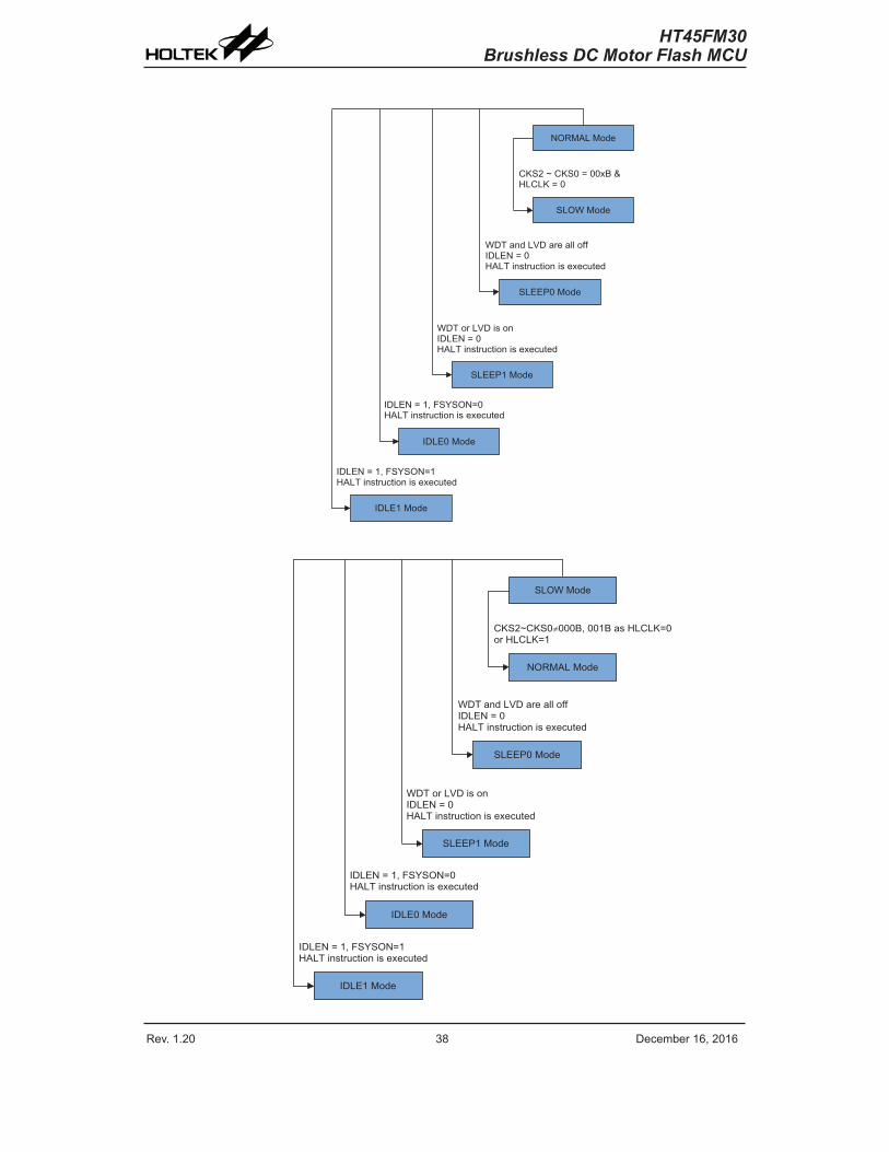
Rev. 1.20 38 De�e��e� 1�� 201� Rev. 1.20 39 De�e��e� 1�� 201�
HT45FM30Brushless DC Motor Flash MCU
� � � � � � � � �
� � � � � � � � � � �
� � � � � � � � � � �
� � � � � � � � � �
� � � � � � � � � �
� � � � � � � � � � �
� � � � � � � � � � � � � � � �� � � � � � �
� � � � � � � � � � � � � � � � � � � � � � �� � � � � � � �� � � � � � � � � � � � � � � � � � � � � � � �
� � � � � � � � � � � � � � � �� � � � � � � �� � � � � � � � � � � � � � � � � � � � � � � �
� � � � � � � � � � � � � � � � �� � � � � � � � � � � � � � � � � � � � � � � �
� � � � � � � � � � � � � � � � �� � � � � � � � � � � � � � � � � � � � � � � �
� � � � � � � � � � �
� � � � � � � � � � �
� � � � � � � � � � �
� � � � � � � � � �
� � � � � � � � � �
� � � � � � � � �
� � � � � � � � � � � � � � � � � � � � � � � � �� � � � � � � � �
� � � � � � � � � � � � � � � � � � � � � � �� � � � � � � � �� � � � � � � � � � � � � � � � � � � � � � � � �
� � � � � � � � � � � � � � � �� � � � � � � � �� � � � � � � � � � � � � � � � � � � � � � � � �
� � � � � � � � � � � � � � � � � � �� � � � � � � � � � � � � � � � � � � � � � � � �
� � � � � � � � � � � � � � � � � � �� � � � � � � � � � � � � � � � � � � � � � � � �
Rev. 1.20 38 De�e��e� 1�� 201� Rev. 1.20 39 De�e��e� 1�� 201�
HT45FM30Brushless DC Motor Flash MCU
SLOW Mode to NORMAL Mode SwitchingInSLOWMode thesystemuses theLIRClowspeedsystemoscillator.Toswitchback to theNORMALMode,wherethehighspeedsystemoscillatorisused,theHLCLKbitshouldbesetto“1”orHLCLKbitis“0”,butCKS2~CKS0issetto“010”,“011”,“100”,“101”,“110”or“111”.Asacertainamountoftimewillberequiredforthehighfrequencyclocktostabilise,thestatusoftheHTObitischecked.Theamountoftimerequiredforhighspeedsystemoscillatorstabilizationdependsuponwhichhighspeedsystemoscillatortypeisused.
Entering the SLEEP ModeThereisonlyonewayforthedevicetoentertheSLEEPModeandthatistoexecutethe"HALT".instructionintheapplicationprogramwiththeIDLENbitinSMODregisterequalto"0"andtheWDTorLVDon.When this instruction isexecutedunder theconditionsdescribedabove, thefollowingwilloccur:
• ThesystemclockandTimeBaseclockwillbestoppedandtheapplicationprogramwillstopatthe"HALT"instruction,buttheWDTorLVDwillremainwiththeclocksourcecomingfromthefSUBclock.
• TheDataMemorycontentsandregisterswillmaintaintheirpresentcondition.
• TheWDTwillbeclearedandresumecountingiftheWDTclocksourceisselectedtocomefromthefSUBclockastheWDTisenabled.
• TheI/Oportswillmaintaintheirpresentconditions.
• Inthestatusregister,thePowerDownflag,PDF,willbesetandtheWatchdogtime-outflag,TO,willbecleared.
Entering the IDLE0 ModeThereisonlyonewayforthedevicetoentertheIDLE0Modeandthatistoexecutethe“HALT”instructionintheapplicationprogramwiththeIDLENbitinSMODregisterequalto“1”andtheFSYSONbitinWDTCregisterequalto“0”.Whenthisinstructionisexecutedundertheconditionsdescribedabove,thefollowingwilloccur:
• Thesystemclockwillbestoppedandtheapplicationprogramwillstopatthe“HALT”instruction,buttheTimeBaseclockandfSUBclockwillbeon.
• TheDataMemorycontentsandregisterswillmaintaintheirpresentcondition.• TheWDTwillbeclearedandresumecountingiftheWDTclocksourceisselectedtocomefromthefSUBclockandtheWDTisenabled.TheWDTwillstopifitsclocksourceoriginatesfromthesystemclock.
• TheI/Oportswillmaintaintheirpresentconditions.• Inthestatusregister,thePowerDownflag,PDF,willbesetandtheWatchdogtime-outflag,TO,willbecleared.
Entering the IDLE1 ModeThereisonlyonewayforthedevicetoentertheIDLE1Modeandthatistoexecutethe“HALT”instructionintheapplicationprogramwiththeIDLENbitinSMODregisterequalto“1”andtheFSYSONbitinWDTCregisterequalto“1”.Whenthisinstructionisexecutedundertheconditionsdescribedabove,thefollowingwilloccur:
• ThesystemclockandTimeBaseclockandfSUBclockwillbeonandtheapplicationprogramwillstopatthe“HALT”instruction.
• TheDataMemorycontentsandregisterswillmaintaintheirpresentcondition.• TheWDTwillbeclearedandresumecounting if theWDTisenabledregardlessof theWDTclocksourcewhichoriginatesfromthefSUBclockorfromthesystemclock.
• TheI/Oportswillmaintaintheirpresentconditions.• Inthestatusregister,thePowerDownflag,PDF,willbesetandtheWatchdogtime-outflag,TO,willbecleared.
Rev. 1.20 40 De�e��e� 1�� 201� Rev. 1.20 41 De�e��e� 1�� 201�
HT45FM30Brushless DC Motor Flash MCU
Standby Current ConsiderationsAsthemainreasonforenteringtheSLEEPorIDLEModeistokeepthecurrentconsumptionofthedevicetoas lowavalueaspossible,perhapsonlyintheorderofseveralmicro-ampsexceptintheIDLE1Mode, thereareotherconsiderationswhichmustalsobetakenintoaccountbythecircuitdesigner if thepowerconsumptionis tobeminimised.SpecialattentionmustbemadetotheI/Opinsonthedevice.Allhigh-impedanceinputpinsmustbeconnectedtoeitherafixedhighor lowlevelasanyfloating inputpinscouldcreate internaloscillationsandresult in increasedcurrentconsumption.Thisalsoappliestodevicewhichhasdifferentpackagetypes,astheremaybeunbondedpins.Thesemusteitherbesetupasoutputsorifsetupasinputsmusthavepull-highresistorsconnected.Caremustalsobetakenwiththeloads,whichareconnectedtoI/Opins,whicharesetupasoutputs.Theseshouldbeplacedinaconditioninwhichminimumcurrentisdrawnorconnectedonlytoexternalcircuitsthatdonotdrawcurrent,suchasotherCMOSinputs.Alsonotethatadditionalstandbycurrentwillalsoberequiredif theconfigurationoptionshaveenabledtheLIRCoscillator.
In theIDLE1Mode thesystemoscillator ison, if thesystemoscillator is fromthehighspeedsystemoscillator,theadditionalstandbycurrentwillalsobeperhapsintheorderofseveralhundredmicro-amps.
Wake-upAfterthesystementerstheSLEEPorIDLEMode,itcanbewokenupfromoneofvarioussourceslistedasfollows:
• AnexternalfallingedgeonPortA
• Asysteminterrupt
• AWDToverflow
If thesystemiswokenupbyanexternal reset, thedevicewillexperiencea full systemreset,however,ifthedeviceiswokenupbyaWDToverflow,aWatchdogTimerresetwillbeinitiated.Althoughbothof thesewake-upmethodswill initiatearesetoperation, theactualsourceof thewake-upcanbedeterminedbyexaminingtheTOandPDFflags.ThePDFflag isclearedbyasystempower-uporexecutingtheclearWatchdogTimerinstructionsandissetwhenexecutingthe“HALT”instruction.TheTOflagissetifaWDTtime-outoccurs,andcausesawake-upthatonlyresetstheProgramCounterandStackPointer,theotherflagsremainintheiroriginalstatus.
EachpinonPortAcanbesetupusingthePAWUregistertopermitanegativetransitiononthepintowake-upthesystem.WhenaPortApinwake-upoccurs,theprogramwillresumeexecutionattheinstructionfollowingthe“HALT”instruction.If thesystemiswokenupbyaninterrupt, thentwopossiblesituationsmayoccur.Thefirstiswheretherelatedinterruptisdisabledortheinterruptisenabledbutthestackisfull,inwhichcasetheprogramwillresumeexecutionattheinstructionfollowingthe“HALT”instruction.Inthissituation,theinterruptwhichwoke-upthedevicewillnotbeimmediatelyserviced,butwillratherbeservicedlaterwhentherelatedinterruptisfinallyenabledorwhenastacklevelbecomesfree.Theothersituationiswheretherelatedinterruptisenabledandthestackisnotfull,inwhichcasetheregularinterruptresponsetakesplace.Ifaninterruptrequestflag issethighbeforeentering theSLEEPorIDLEMode, thewake-upfunctionof therelatedinterruptwillbedisabled.
Rev. 1.20 40 De�e��e� 1�� 201� Rev. 1.20 41 De�e��e� 1�� 201�
HT45FM30Brushless DC Motor Flash MCU
Watchdog TimerTheWatchdogTimerisprovidedtopreventprogrammalfunctionsorsequencesfromjumpingtounknownlocations,duetocertainuncontrollableexternaleventssuchaselectricalnoise.
Watchdog Timer Clock SourceTheWatchdogTimerclocksource isprovidedby the internal lowspeedoscillator, fLIRC.TheWatchdogTimersourceclockis thensubdividedbyaratioof28 to215 togive longer timeouts,theactualvaluebeingchosenusingtheWS2~WS0bitsintheWDTCregister.TheLIRCinternaloscillatorhasanapproximateperiodof32kHzatasupplyvoltageof5V.
However,itshouldbenotedthatthisspecifiedinternalclockperiodcanvarywithVDD,temperatureandprocessvariations.
Watchdog Timer Control RegisterAsingleregister,WDTC,controlstherequiredtime-outperiod.
WDTC Register
Bit 7 6 5 4 3 2 1 0Na�e FSYSON WS2 WS1 WS0 D3 D2 D1 D0R/W R/W R/W R/W R/W R/W R/W R/W R/WPOR 0 1 1 1 1 0 1 0
Bit7 FSYSON:fSYScontrolinIDLEMode0:disable1:enable
Bit6~4 WS2~WS0:WDTTime-outPeriodSelection000:256/fLIRC001:512/fLIRC010:1024/fLIRC011:2048/fLIRC100:4096/fLIRC101:8192/fLIRC110:16384/fLIRC111:32768/fLIRCThese threebitsdetermine thedivisionratioof theWatchdogTimersourceclock,whichinturndeterminesthetime-outperiod.
Bit3~0 UndefinedbitThesebitscanbereadorwrittenbyusersoftwareprogram.
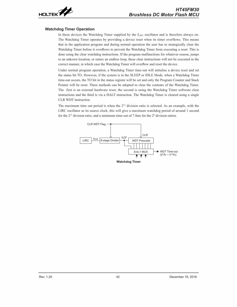
Rev. 1.20 42 De�e��e� 1�� 201� Rev. 1.20 43 De�e��e� 1�� 201�
HT45FM30Brushless DC Motor Flash MCU
Watchdog Timer OperationIn thesedevices theWatchdogTimersuppliedbythefLIRCoscillatorandis thereforealwayson.TheWatchdogTimeroperatesbyprovidingadeviceresetwhenits timeroverflows.ThismeansthatintheapplicationprogramandduringnormaloperationtheuserhastostrategicallycleartheWatchdogTimerbeforeitoverflowstopreventtheWatchdogTimerfromexecutingareset.Thisisdoneusingtheclearwatchdoginstructions.Iftheprogrammalfunctionsforwhateverreason,jumpstoanunkownlocation,orentersanendlessloop,theseclearinstructionswillnotbeexecutedinthecorrectmanner,inwhichcasetheWatchdogTimerwilloverflowandresetthedevice.
Undernormalprogramoperation,aWatchdogTimertime-outwill initialiseadeviceresetandsetthestatusbitTO.However,ifthesystemisintheSLEEPorIDLEMode,whenaWatchdogTimertime-outoccurs,theTObitinthestatusregisterwillbesetandonlytheProgramCounterandStackPointerwillbereset.ThreemethodscanbeadoptedtoclearthecontentsoftheWatchdogTimer.The first isanexternalhardwarereset, thesecondisusing theWatchdogTimersoftwareclearinstructionsandthethirdisviaaHALTinstruction.TheWatchdogTimerisclearedusingasingleCLRWDTinstruction.
Themaximumtimeoutperiodiswhenthe215divisionratioisselected.Asanexample,withtheLIRCoscillatorasitssourceclock,thiswillgiveamaximumwatchdogperiodofaround1secondforthe215divisionratio,andaminimumtime-outof7.8msforthe28divisionration.
� � � � � � � � � � � � � � �
� � � � � � � � � � � � � � � � � � � � � � �
� � �
� � � � � � � � � � � � �
� � � � � � � � � �
� � � � � � � � � � � �
� � � � �
� � � � � � � � � � � � � � �
� � � �
Watchdog Timer
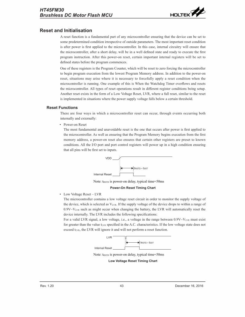
Rev. 1.20 42 De�e��e� 1�� 201� Rev. 1.20 43 De�e��e� 1�� 201�
HT45FM30Brushless DC Motor Flash MCU
Reset and InitialisationAresetfunctionisafundamentalpartofanymicrocontrollerensuringthatthedevicecanbesettosomepredeterminedconditionirrespectiveofoutsideparameters.Themostimportantresetconditionisafterpowerisfirstappliedtothemicrocontroller.Inthiscase,internalcircuitrywillensurethatthemicrocontroller,afterashortdelay,willbeinawelldefinedstateandreadytoexecutethefirstprograminstruction.After thispower-onreset,certain important internalregisterswillbeset todefinedstatesbeforetheprogramcommences.
OneoftheseregistersistheProgramCounter,whichwillberesettozeroforcingthemicrocontrollertobeginprogramexecutionfromthelowestProgramMemoryaddress.Inadditiontothepower-onreset, situationsmayarisewhere it isnecessary to forcefullyapplya resetconditionwhen themicrocontrollerisrunning.OneexampleofthisisWhentheWatchdogTimeroverflowsandresetsthemicrocontroller.Alltypesofresetoperationsresultindifferentregisterconditionsbeingsetup.AnotherresetexistsintheformofaLowVoltageReset,LVR,whereafullreset,similartotheresetisimplementedinsituationswherethepowersupplyvoltagefallsbelowacertainthreshold.
Reset FunctionsThereare fourways inwhichamicrocontroller resetcanoccur, througheventsoccurringbothinternallyandexternally:
• Power-onResetThemostfundamentalandunavoidableresetistheonethatoccursafterpowerisfirstappliedtothemicrocontroller.AswellasensuringthattheProgramMemorybeginsexecutionfromthefirstmemoryaddress,apower-onresetalsoensuresthatcertainotherregistersarepreset toknownconditions.AlltheI/Oportandportcontrolregisterswillpowerupinahighconditionensuringthatallpinswillbefirstsettoinputs.
� � �
� � � � � � � � � � � � � �
� � � � � � � � � � � �� � � � � � � � � � � �
Note:tRSTDispower-ondelay,typicaltime=50ms
Power-On Reset Timing Chart
• LowVoltageReset–LVRThemicrocontrollercontainsalowvoltageresetcircuitinordertomonitorthesupplyvoltageofthedevice,whichisselectedasVLVR.Ifthesupplyvoltageofthedevicedropstowithinarangeof0.9V~VLVRsuchasmightoccurwhenchangingthebattery,theLVRwillautomaticallyresetthedeviceinternally.TheLVRincludesthefollowingspecifications:ForavalidLVRsignal,alowvoltage,i.e.,avoltageintherangebetween0.9V~VLVRmustexistforgreaterthanthevaluetLVRspecifiedintheA.C.characteristics.IfthelowvoltagestatedoesnotexceedtLVR,theLVRwillignoreitandwillnotperformaresetfunction.
� � �
� � � � � � � � � � � � � �
� � � � � � � � � � � �
Note:tRSTDispower-ondelay,typicaltime=50ms
Low Voltage Reset Timing Chart
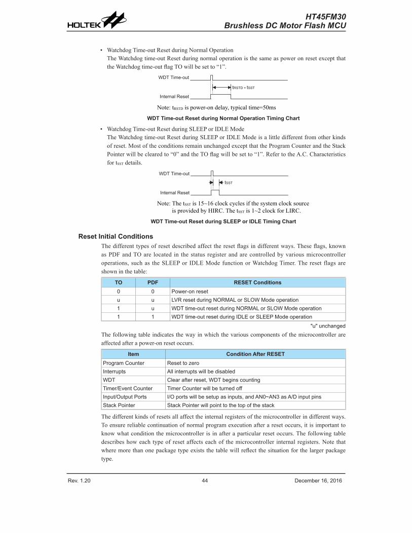
Rev. 1.20 44 De�e��e� 1�� 201� Rev. 1.20 45 De�e��e� 1�� 201�
HT45FM30Brushless DC Motor Flash MCU
• WatchdogTime-outResetduringNormalOperationTheWatchdogtime-outResetduringnormaloperationisthesameaspoweronresetexceptthattheWatchdogtime-outflagTOwillbesetto“1”.
� � � � � � � � � � � �
� � � � � � � � � � � �
� � � � � � � � � � � � �
Note:tRSTDispower-ondelay,typicaltime=50ms
WDT Time-out Reset during Normal Operation Timing Chart
• WatchdogTime-outResetduringSLEEPorIDLEModeTheWatchdogtime-outResetduringSLEEPorIDLEModeisalittledifferentfromotherkindsofreset.MostoftheconditionsremainunchangedexceptthattheProgramCounterandtheStackPointerwillbeclearedto“0”andtheTOflagwillbesetto“1”.RefertotheA.C.CharacteristicsfortSSTdetails.
� � � �
� � � � � � � � � � � �
� � � � � � � � � � � � �
Note:ThetSSTis15~16clockcyclesifthesystemclocksourceisprovidedbyHIRC.ThetSSTis1~2clockforLIRC.
WDT Time-out Reset during SLEEP or IDLE Timing Chart
Reset Initial ConditionsThedifferent typesofresetdescribedaffect theresetflagsindifferentways.Theseflags,knownasPDFandTOare located in thestatus registerandarecontrolledbyvariousmicrocontrolleroperations,suchas theSLEEPorIDLEModefunctionorWatchdogTimer.Thereset flagsareshowninthetable:
TO PDF RESET Conditions0 0 Powe�-on �esetu u LVR �eset du�ing NORMAL o� SLOW Mode ope�ation1 u WDT ti�e-out �eset du�ing NORMAL o� SLOW Mode ope�ation1 1 WDT ti�e-out �eset du�ing IDLE o� SLEEP Mode ope�ation
"u" un�hangedThefollowingtableindicatesthewayinwhichthevariouscomponentsofthemicrocontrollerareaffectedafterapower-onresetoccurs.
Item Condition After RESETP�og�a� Counte� Reset to ze�oInte��upts All inte��upts will �e disa�ledWDT Clea� afte� �eset� WDT �egins �ountingTi�e�/Event Counte� Ti�e� Counte� will �e tu�ned offInput/Output Po�ts I/O po�ts will �e setup as inputs� and AN0~AN3 as A/D input pinsSta�k Pointe� Sta�k Pointe� will point to the top of the sta�k
Thedifferentkindsofresetsallaffecttheinternalregistersofthemicrocontrollerindifferentways.Toensurereliablecontinuationofnormalprogramexecutionafteraresetoccurs,itisimportanttoknowwhatconditionthemicrocontrolleris inafteraparticularresetoccurs.Thefollowingtabledescribeshoweachtypeofresetaffectseachof themicrocontroller internalregisters.Note thatwheremorethanonepackagetypeexiststhetablewillreflectthesituationforthelargerpackagetype.
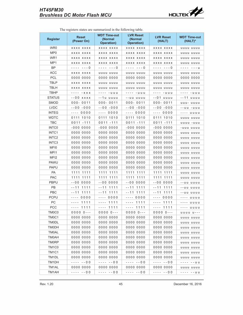
Rev. 1.20 44 De�e��e� 1�� 201� Rev. 1.20 45 De�e��e� 1�� 201�
HT45FM30Brushless DC Motor Flash MCU
Theregistersstatesaresummarizedinthefollowingtable.
Register Reset(Power On)
WDT Time-out(Normal
Operation)
LVR Reset (Normal
Operation)
LVR Reset (HALT)
WDT Time-out (HALT)*
IAR0 x x x x x x x x x x x x x x x x x x x x x x x x x x x x x x x x u u u u u u u uMP0 x x x x x x x x x x x x x x x x x x x x x x x x x x x x x x x x u u u u u u u uIAR1 x x x x x x x x x x x x x x x x x x x x x x x x x x x x x x x x u u u u u u u uMP1 x x x x x x x x x x x x x x x x x x x x x x x x x x x x x x x x u u u u u u u uBP - - - - - - - 0 - - - - - - - 0 - - - - - - - 0 - - - - - - - 0 - - - - - - - u
ACC x x x x x x x x u u u u u u u u u u u u u u u u u u u u u u u u u u u u u u u uPCL 0 0 0 0 0 0 0 0 0 0 0 0 0 0 0 0 0 0 0 0 0 0 0 0 0 0 0 0 0 0 0 0 0 0 0 0 0 0 0 0
TBLP x x x x x x x x u u u u u u u u u u u u u u u u u u u u u u u u u u u u u u u uTBLH x x x x x x x x u u u u u u u u u u u u u u u u u u u u u u u u u u u u u u u uTBHP - - - - - x x x - - - - - u u u - - - - - u u u - - - - - u u u - - - - - u u u
STATUS - - 0 0 x x x x - - 1 u u u u u - - u u u u u u - - 0 1 u u u u - - 1 1 u u u uSMOD 0 0 0 - 0 0 11 0 0 0 - 0 0 11 0 0 0 - 0 0 11 0 0 0 - 0 0 11 u u u - u u u uLVDC - - 0 0 - 0 0 0 - - 0 0 - 0 0 0 - - 0 0 - 0 0 0 - - 0 0 - 0 0 0 - - u u - u u uINTEG - - - - 0 0 0 0 - - - - 0 0 0 0 - - - - 0 0 0 0 - - - - 0 0 0 0 - - - - u u u uWDTC 0 111 1 0 1 0 0 111 1 0 1 0 0 111 1 0 1 0 0 111 1 0 1 0 u u u u u u u uTBC 0 0 1 1 - 1 1 1 0 0 1 1 - 1 1 1 0 0 1 1 - 1 1 1 0 0 1 1 - 1 1 1 u u u u - u u u
INTC0 - 0 0 0 0 0 0 0 - 0 0 0 0 0 0 0 - 0 0 0 0 0 0 0 - 0 0 0 0 0 0 0 - u u u u u u uINTC1 0 0 0 0 0 0 0 0 0 0 0 0 0 0 0 0 0 0 0 0 0 0 0 0 0 0 0 0 0 0 0 0 u u u u u u u uINTC2 0 0 0 0 0 0 0 0 0 0 0 0 0 0 0 0 0 0 0 0 0 0 0 0 0 0 0 0 0 0 0 0 u u u u u u u uINTC3 0 0 0 0 0 0 0 0 0 0 0 0 0 0 0 0 0 0 0 0 0 0 0 0 0 0 0 0 0 0 0 0 u u u u u u u uMFI0 0 0 0 0 0 0 0 0 0 0 0 0 0 0 0 0 0 0 0 0 0 0 0 0 0 0 0 0 0 0 0 0 u u u u u u u uMFI1 0 0 0 0 0 0 0 0 0 0 0 0 0 0 0 0 0 0 0 0 0 0 0 0 0 0 0 0 0 0 0 0 u u u u u u u uMFI2 0 0 0 0 0 0 0 0 0 0 0 0 0 0 0 0 0 0 0 0 0 0 0 0 0 0 0 0 0 0 0 0 u u u u u u u u
PAWU 0 0 0 0 0 0 0 0 0 0 0 0 0 0 0 0 0 0 0 0 0 0 0 0 0 0 0 0 0 0 0 0 u u u u u u u uPAPU 0 0 0 0 0 0 0 0 0 0 0 0 0 0 0 0 0 0 0 0 0 0 0 0 0 0 0 0 0 0 0 0 u u u u u u u u
PA 1 1 1 1 1 1 1 1 1 1 1 1 1 1 1 1 1 1 1 1 1 1 1 1 1 1 1 1 1 1 1 1 u u u u u u u uPAC 1 1 1 1 1 1 1 1 1 1 1 1 1 1 1 1 1 1 1 1 1 1 1 1 1 1 1 1 1 1 1 1 u u u u u u u u
PBPU - - 0 0 0 0 0 0 - - 0 0 0 0 0 0 - - 0 0 0 0 0 0 - - 0 0 0 0 0 0 - - u u u u u uPB - - 1 1 1 1 1 1 - - 1 1 1 1 1 1 - - 1 1 1 1 1 1 - - 1 1 1 1 1 1 - - u u u u u u
PBC - - 1 1 1 1 1 1 - - 1 1 1 1 1 1 - - 1 1 1 1 1 1 - - 1 1 1 1 1 1 - - u u u u u uPCPU - - - - 0 0 0 0 - - - - 0 0 0 0 - - - - 0 0 0 0 - - - - 0 0 0 0 - - - - u u u u
PC - - - - 1 1 1 1 - - - - 1 1 1 1 - - - - 1 1 1 1 - - - - 1 1 1 1 - - - - u u u uPCC - - - - 1 1 1 1 - - - - 1 1 1 1 - - - - 1 1 1 1 - - - - 1 1 1 1 - - - - u u u u
TM0C0 0 0 0 0 0 - - - 0 0 0 0 0 - - - 0 0 0 0 0 - - - 0 0 0 0 0 - - - u u u u u - - -TM0C1 0 0 0 0 0 0 0 0 0 0 0 0 0 0 0 0 0 0 0 0 0 0 0 0 0 0 0 0 0 0 0 0 u u u u u u u uTM0DL 0 0 0 0 0 0 0 0 0 0 0 0 0 0 0 0 0 0 0 0 0 0 0 0 0 0 0 0 0 0 0 0 u u u u u u u uTM0DH 0 0 0 0 0 0 0 0 0 0 0 0 0 0 0 0 0 0 0 0 0 0 0 0 0 0 0 0 0 0 0 0 u u u u u u u uTM0AL 0 0 0 0 0 0 0 0 0 0 0 0 0 0 0 0 0 0 0 0 0 0 0 0 0 0 0 0 0 0 0 0 u u u u u u u uTM0AH 0 0 0 0 0 0 0 0 0 0 0 0 0 0 0 0 0 0 0 0 0 0 0 0 0 0 0 0 0 0 0 0 u u u u u u u uTM0RP 0 0 0 0 0 0 0 0 0 0 0 0 0 0 0 0 0 0 0 0 0 0 0 0 0 0 0 0 0 0 0 0 u u u u u u u uTM1C0 0 0 0 0 0 0 0 0 0 0 0 0 0 0 0 0 0 0 0 0 0 0 0 0 0 0 0 0 0 0 0 0 u u u u u u u uTM1C1 0 0 0 0 0 0 0 0 0 0 0 0 0 0 0 0 0 0 0 0 0 0 0 0 0 0 0 0 0 0 0 0 u u u u u u u uTM1DL 0 0 0 0 0 0 0 0 0 0 0 0 0 0 0 0 0 0 0 0 0 0 0 0 0 0 0 0 0 0 0 0 u u u u u u u uTM1DH - - - - - - 0 0 - - - - - - 0 0 - - - - - - 0 0 - - - - - - 0 0 - - - - - - u uTM1AL 0 0 0 0 0 0 0 0 0 0 0 0 0 0 0 0 0 0 0 0 0 0 0 0 0 0 0 0 0 0 0 0 u u u u u u u uTM1AH - - - - - - 0 0 - - - - - - 0 0 - - - - - - 0 0 - - - - - - 0 0 - - - - - - u u
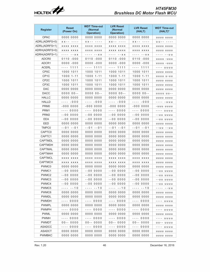
Rev. 1.20 4� De�e��e� 1�� 201� Rev. 1.20 47 De�e��e� 1�� 201�
HT45FM30Brushless DC Motor Flash MCU
Register Reset(Power On)
WDT Time-out(Normal
Operation)
LVR Reset (Normal
Operation)
LVR Reset (HALT)
WDT Time-out (HALT)*
OPAC 0 0 0 0 0 0 0 0 0 0 0 0 0 0 0 0 0 0 0 0 0 0 0 0 0 0 0 0 0 0 0 0 u u u u u u u uADRL(ADRFS=0) x x - - - - - - x x - - - - - - x x - - - - - - x x - - - - - - u u - - - - - -ADRL(ADRFS=1) x x x x x x x x x x x x x x x x x x x x x x x x x x x x x x x x u u u u u u u uADRH(ADRFS=0) x x x x x x x x x x x x x x x x x x x x x x x x x x x x x x x x u u u u u u u uADRH(ADRFS=1) - - - - - - x x - - - - - - x x - - - - - - x x - - - - - - x x - - - - - - u u
ADCR0 0 11 0 - 0 0 0 0 11 0 - 0 0 0 0 11 0 - 0 0 0 0 11 0 - 0 0 0 u u u u - u u uADCR1 0 0 0 0 - 0 0 0 0 0 0 0 - 0 0 0 0 0 0 0 - 0 0 0 0 0 0 0 - 0 0 0 u u u u - u u uACERL - - - - 1 1 1 1 - - - - 1 1 1 1 - - - - 1 1 1 1 - - - - 1 1 1 1 - - - - u u u uCP0C 1 0 0 0 1 0 11 1 0 0 0 1 0 11 1 0 0 0 1 0 11 1 0 0 0 1 0 11 u u u u u u u uCP1C 1 0 0 0 1 - 11 1 0 0 0 1 - 11 1 0 0 0 1 - 11 1 0 0 0 1 - 11 u u u u u - u uCP2C 1 0 0 0 1 0 11 1 0 0 0 1 0 11 1 0 0 0 1 0 11 1 0 0 0 1 0 11 u u u u u u u uCP3C 1 0 0 0 1 0 11 1 0 0 0 1 0 11 1 0 0 0 1 0 11 1 0 0 0 1 0 11 u u u u u u u uDAC 0 0 0 0 0 0 0 0 0 0 0 0 0 0 0 0 0 0 0 0 0 0 0 0 0 0 0 0 0 0 0 0 u u u u u u u u
DACC 0 0 0 0 0 0 - - 0 0 0 0 0 0 - - 0 0 0 0 0 0 - - 0 0 0 0 0 0 - - u u u u u u - -HALLC 0 0 0 0 0 0 0 0 0 0 0 0 0 0 0 0 0 0 0 0 0 0 0 0 0 0 0 0 0 0 0 0 u u u u u u u uHALLD - - - - - 0 0 0 - - - - - 0 0 0 - - - - - 0 0 0 - - - - - 0 0 0 - - - - - u u uPRM0 - 0 0 0 0 0 0 0 - 0 0 0 0 0 0 0 - 0 0 0 0 0 0 0 - 0 0 0 0 0 0 0 - u u u u u u uPRM1 - - - - 0 0 0 0 - - - - 0 0 0 0 - - - - 0 0 0 0 - - - - 0 0 0 0 - - - - u u u uPRM2 - - 0 0 0 0 0 0 - - 0 0 0 0 0 0 - - 0 0 0 0 0 0 - - 0 0 0 0 0 0 - - u u u u u uEEA - - 0 0 0 0 0 0 - - 0 0 0 0 0 0 - - 0 0 0 0 0 0 - - 0 0 0 0 0 0 - - u u u u u uEED 0 0 0 0 0 0 0 0 0 0 0 0 0 0 0 0 0 0 0 0 0 0 0 0 0 0 0 0 0 0 0 0 u u u u u u u u
TMPC0 - - 0 1 - - 0 1 - - 0 1 - - 0 1 - - 0 1 - - 0 1 - - 0 1 - - 0 1 - - u u - - u uCAPTC0 0 0 0 0 0 0 0 0 0 0 0 0 0 0 0 0 0 0 0 0 0 0 0 0 0 0 0 0 0 0 0 0 u u u u u u u uCAPTC1 0 0 0 0 0 0 0 0 0 0 0 0 0 0 0 0 0 0 0 0 0 0 0 0 0 0 0 0 0 0 0 0 u u u u u u u u
CAPTMDL 0 0 0 0 0 0 0 0 0 0 0 0 0 0 0 0 0 0 0 0 0 0 0 0 0 0 0 0 0 0 0 0 u u u u u u u uCAPTMDH 0 0 0 0 0 0 0 0 0 0 0 0 0 0 0 0 0 0 0 0 0 0 0 0 0 0 0 0 0 0 0 0 u u u u u u u uCAPTMAL 0 0 0 0 0 0 0 0 0 0 0 0 0 0 0 0 0 0 0 0 0 0 0 0 0 0 0 0 0 0 0 0 u u u u u u u uCAPTMAH 0 0 0 0 0 0 0 0 0 0 0 0 0 0 0 0 0 0 0 0 0 0 0 0 0 0 0 0 0 0 0 0 u u u u u u u uCAPTMCL x x x x x x x x x x x x x x x x x x x x x x x x x x x x x x x x u u u u u u u uCAPTMCH x x x x x x x x x x x x x x x x x x x x x x x x x x x x x x x x u u u u u u u u
PWMC0 0 0 0 0 0 0 0 0 0 0 0 0 0 0 0 0 0 0 0 0 0 0 0 0 0 0 0 0 0 0 0 0 u u u u u u u uPWMC1 - - 0 0 0 0 0 0 - - 0 0 0 0 0 0 - - 0 0 0 0 0 0 - - 0 0 0 0 0 0 - - u u u u u uPWMC2 - - 0 0 0 0 0 0 - - 0 0 0 0 0 0 - - 0 0 0 0 0 0 - - 0 0 0 0 0 0 - - u u u u u uPWMC3 - - 0 0 0 0 0 0 - - 0 0 0 0 0 0 - - 0 0 0 0 0 0 - - 0 0 0 0 0 0 - - u u u u u uPWMC4 - - 0 0 0 0 0 0 - - 0 0 0 0 0 0 - - 0 0 0 0 0 0 - - 0 0 0 0 0 0 - - u u u u u uPWMC5 - - - - - - 1 0 - - - - - - 1 0 - - - - - - 1 0 - - - - - - 1 0 - - - - - - u uPWMC� 0 0 0 0 0 0 0 0 0 0 0 0 0 0 0 0 0 0 0 0 0 0 0 0 0 0 0 0 0 0 0 0 u u u u u u u uPWMDL 0 0 0 0 0 0 0 0 0 0 0 0 0 0 0 0 0 0 0 0 0 0 0 0 0 0 0 0 0 0 0 0 u u u u u u u uPWMDH - - - - 0 0 0 0 - - - - 0 0 0 0 - - - - 0 0 0 0 - - - - 0 0 0 0 - - - - u u u uPWMPL 0 0 0 0 0 0 0 0 0 0 0 0 0 0 0 0 0 0 0 0 0 0 0 0 0 0 0 0 0 0 0 0 u u u u u u u uPWMPH - - - - 0 0 0 0 - - - - 0 0 0 0 - - - - 0 0 0 0 - - - - 0 0 0 0 - - - - u u u uPWML 0 0 0 0 0 0 0 0 0 0 0 0 0 0 0 0 0 0 0 0 0 0 0 0 0 0 0 0 0 0 0 0 u u u u u u u uPWMH - - - - 0 0 0 0 - - - - 0 0 0 0 - - - - 0 0 0 0 - - - - 0 0 0 0 - - - - u u u u
PWMDT 0 0 - - 0 0 0 0 0 0 - - 0 0 0 0 0 0 - - 0 0 0 0 0 0 - - 0 0 0 0 u u - - u u u uASADCC - - - - 0 0 0 0 - - - - 0 0 0 0 - - - - 0 0 0 0 - - - - 0 0 0 0 - - - - u u u uASADCT 0 0 0 0 0 0 0 0 0 0 0 0 0 0 0 0 0 0 0 0 0 0 0 0 0 0 0 0 0 0 0 0 u u u u u u u uPWMBKC 0 0 0 0 0 0 0 0 0 0 0 0 0 0 0 0 0 0 0 0 0 0 0 0 0 0 0 0 0 0 0 0 u u u u u u u u
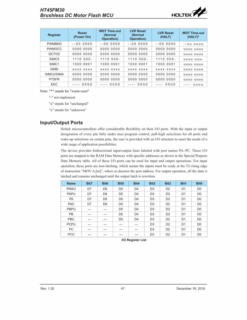
Rev. 1.20 4� De�e��e� 1�� 201� Rev. 1.20 47 De�e��e� 1�� 201�
HT45FM30Brushless DC Motor Flash MCU
Register Reset(Power On)
WDT Time-out(Normal
Operation)
LVR Reset (Normal
Operation)
LVR Reset (HALT)
WDT Time-out (HALT)*
PWMBKD - - 0 0 0 0 0 0 - - 0 0 0 0 0 0 - - 0 0 0 0 0 0 - - 0 0 0 0 0 0 - - u u u u u uPWMOCC 0 0 0 0 0 0 0 0 0 0 0 0 0 0 0 0 0 0 0 0 0 0 0 0 0 0 0 0 0 0 0 0 u u u u u u u uI2CTOC 0 0 0 0 0 0 0 0 0 0 0 0 0 0 0 0 0 0 0 0 0 0 0 0 0 0 0 0 0 0 0 0 u u u u u u u uSIMC0 111 0 0 0 0 - 111 0 0 0 0 - 111 0 0 0 0 - 111 0 0 0 0 - u u u u u u u -SIMC1 1 0 0 0 0 0 0 1 1 0 0 0 0 0 0 1 1 0 0 0 0 0 0 1 1 0 0 0 0 0 0 1 u u u u u u u uSIMD x x x x x x x x x x x x x x x x x x x x x x x x x x x x x x x x u u u u u u u u
SIMC2/SIMA 0 0 0 0 0 0 0 0 0 0 0 0 0 0 0 0 0 0 0 0 0 0 0 0 0 0 0 0 0 0 0 0 u u u u u u u uPTSFR 0 0 0 0 0 0 0 0 0 0 0 0 0 0 0 0 0 0 0 0 0 0 0 0 0 0 0 0 0 0 0 0 u u u u u u u u
EEC - - - - 0 0 0 0 - - - - 0 0 0 0 - - - - 0 0 0 0 - - - - 0 0 0 0 - - - - u u u u
Note:"*"standsfor"warmreset"
"-"notimplement
"u"standsfor"unchanged"
"x"standsfor"unknown"
Input/Output PortsHoltekmicrocontrollersofferconsiderableflexibilityontheirI/Oports.Withtheinputoroutputdesignationofeverypinfullyunderuserprogramcontrol,pull-highselectionsforallportsandwake-upselectionsoncertainpins,theuserisprovidedwithanI/Ostructuretomeettheneedsofawiderangeofapplicationpossibilities.
Thedeviceprovidesbidirectional input/output lines labeledwithportnamesPA~PC.TheseI/OportsaremappedtotheRAMDataMemorywithspecificaddressesasshownintheSpecialPurposeDataMemorytable.Allof theseI/Oportscanbeusedforinputandoutputoperations.Forinputoperation,theseportsarenon-latching,whichmeanstheinputsmustbereadyattheT2risingedgeofinstruction“MOVA,[m]”,wheremdenotestheportaddress.Foroutputoperation,allthedataislatchedandremainsunchangeduntiltheoutputlatchisrewritten.
Name Bit7 Bit6 Bit5 Bit4 Bit3 Bit2 Bit1 Bit0PAWU D7 D� D5 D4 D3 D2 D1 D0PAPU D7 D� D5 D4 D3 D2 D1 D0
PA D7 D� D5 D4 D3 D2 D1 D0PAC D7 D� D5 D4 D3 D2 D1 D0
PBPU — — D5 D4 D3 D2 D1 D0PB — — D5 D4 D3 D2 D1 D0
PBC — — D5 D4 D3 D2 D1 D0PCPU — — — — D3 D2 D1 D0
PC — — — — D3 D2 D1 D0PCC — — — — D3 D2 D1 D0
I/O Register List
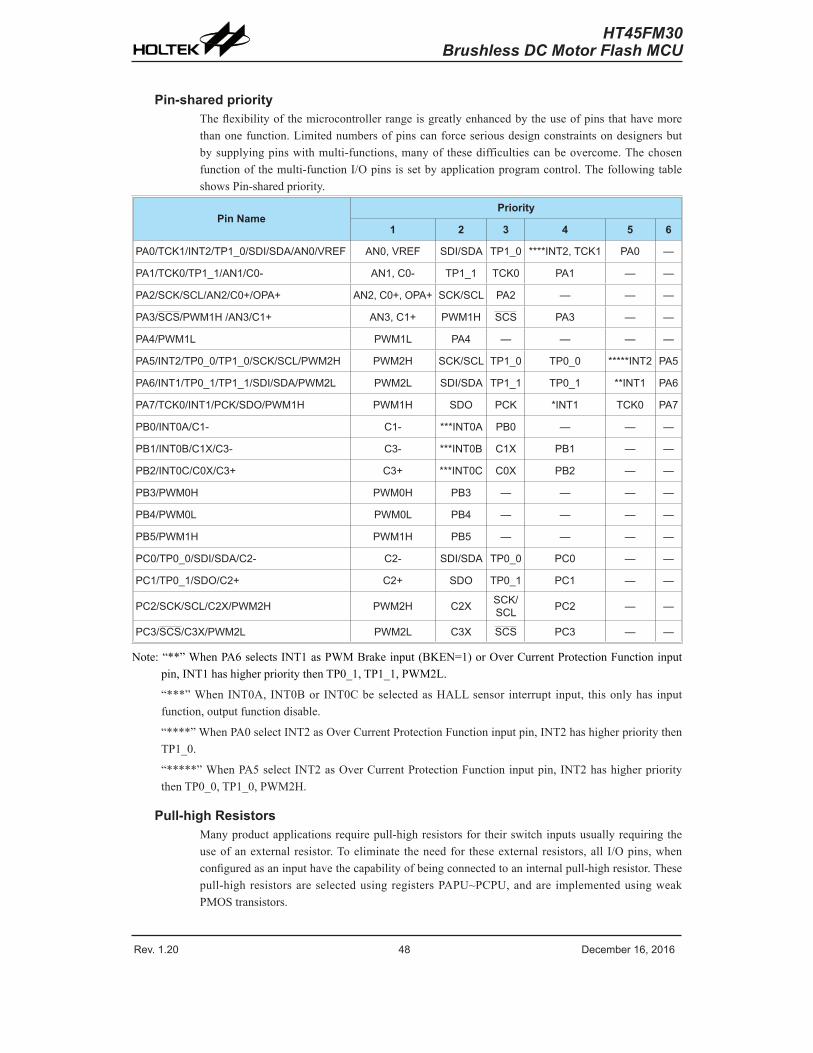
Rev. 1.20 48 De�e��e� 1�� 201� Rev. 1.20 49 De�e��e� 1�� 201�
HT45FM30Brushless DC Motor Flash MCU
Pin-shared priorityTheflexibilityofthemicrocontrollerrangeisgreatlyenhancedbytheuseofpinsthathavemorethanonefunction.Limitednumbersofpinscanforceseriousdesignconstraintsondesignersbutbysupplyingpinswithmulti-functions,manyof thesedifficultiescanbeovercome.Thechosenfunctionofthemulti-functionI/Opinsissetbyapplicationprogramcontrol.ThefollowingtableshowsPin-sharedpriority.
Pin NamePriority
1 2 3 4 5 6
PA0/TCK1/INT2/TP1_0/SDI/SDA/AN0/VREF AN0� VREF SDI/SDA TP1_0 ****INT2� TCK1 PA0 —
PA1/TCK0/TP1_1/AN1/C0- AN1� C0- TP1_1 TCK0 PA1 — —
PA2/SCK/SCL/AN2/C0+/OPA+ AN2� C0+� OPA+ SCK/SCL PA2 — — —
PA3/SCS/PWM1H /AN3/C1+ AN3� C1+ PWM1H SCS PA3 — —
PA4/PWM1L PWM1L PA4 — — — —
PA5/INT2/TP0_0/TP1_0/SCK/SCL/PWM2H PWM2H SCK/SCL TP1_0 TP0_0 *****INT2 PA5
PA�/INT1/TP0_1/TP1_1/SDI/SDA/PWM2L PWM2L SDI/SDA TP1_1 TP0_1 **INT1 PA�
PA7/TCK0/INT1/PCK/SDO/PWM1H PWM1H SDO PCK *INT1 TCK0 PA7
PB0/INT0A/C1- C1- ***INT0A PB0 — — —
PB1/INT0B/C1X/C3- C3- ***INT0B C1X PB1 — —
PB2/INT0C/C0X/C3+ C3+ ***INT0C C0X PB2 — —
PB3/PWM0H PWM0H PB3 — — — —
PB4/PWM0L PWM0L PB4 — — — —
PB5/PWM1H PWM1H PB5 — — — —
PC0/TP0_0/SDI/SDA/C2- C2- SDI/SDA TP0_0 PC0 — —
PC1/TP0_1/SDO/C2+ C2+ SDO TP0_1 PC1 — —
PC2/SCK/SCL/C2X/PWM2H PWM2H C2X SCK/SCL PC2 — —
PC3/SCS/C3X/PWM2L PWM2L C3X SCS PC3 — —
Note:“**”WhenPA6selectsINT1asPWMBrakeinput(BKEN=1)orOverCurrentProtectionFunctioninputpin,INT1hashigherprioritythenTP0_1,TP1_1,PWM2L.
“***”WhenINT0A,INT0BorINT0CbeselectedasHALLsensor interrupt input, thisonlyhas inputfunction,outputfunctiondisable.
“****”WhenPA0selectINT2asOverCurrentProtectionFunctioninputpin,INT2hashigherprioritythenTP1_0.
“*****”WhenPA5selectINT2asOverCurrentProtectionFunctioninputpin,INT2hashigherprioritythenTP0_0,TP1_0,PWM2H.
Pull-high ResistorsManyproductapplicationsrequirepull-highresistorsfortheirswitchinputsusuallyrequiringtheuseofanexternal resistor.Toeliminate theneedfor theseexternal resistors,all I/Opins,whenconfiguredasaninputhavethecapabilityofbeingconnectedtoaninternalpull-highresistor.Thesepull-highresistorsareselectedusingregistersPAPU~PCPU,andare implementedusingweakPMOStransistors.
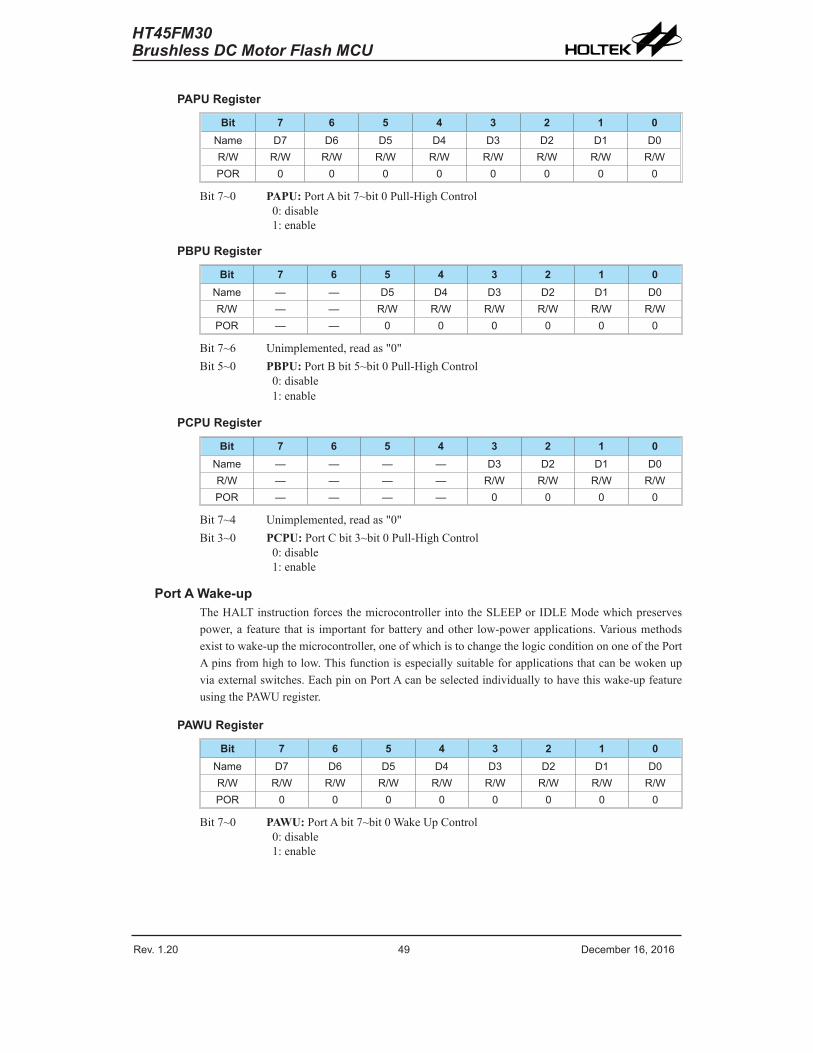
Rev. 1.20 48 De�e��e� 1�� 201� Rev. 1.20 49 De�e��e� 1�� 201�
HT45FM30Brushless DC Motor Flash MCU
PAPU Register
Bit 7 6 5 4 3 2 1 0Na�e D7 D� D5 D4 D3 D2 D1 D0R/W R/W R/W R/W R/W R/W R/W R/W R/WPOR 0 0 0 0 0 0 0 0
Bit7~0 PAPU:PortAbit7~bit0Pull-HighControl0:disable1:enable
PBPU Register
Bit 7 6 5 4 3 2 1 0Na�e — — D5 D4 D3 D2 D1 D0R/W — — R/W R/W R/W R/W R/W R/WPOR — — 0 0 0 0 0 0
Bit7~6 Unimplemented,readas"0"Bit5~0 PBPU:PortBbit5~bit0Pull-HighControl
0:disable1:enable
PCPU Register
Bit 7 6 5 4 3 2 1 0Na�e — — — — D3 D2 D1 D0R/W — — — — R/W R/W R/W R/WPOR — — — — 0 0 0 0
Bit7~4 Unimplemented,readas"0"Bit3~0 PCPU:PortCbit3~bit0Pull-HighControl
0:disable1:enable
Port A Wake-upTheHALTinstructionforcesthemicrocontrollerintotheSLEEPorIDLEModewhichpreservespower,afeature that is importantforbatteryandother low-powerapplications.Variousmethodsexisttowake-upthemicrocontroller,oneofwhichistochangethelogicconditionononeofthePortApinsfromhightolow.Thisfunctionisespeciallysuitableforapplicationsthatcanbewokenupviaexternalswitches.EachpinonPortAcanbeselectedindividuallytohavethiswake-upfeatureusingthePAWUregister.
PAWU Register
Bit 7 6 5 4 3 2 1 0Na�e D7 D� D5 D4 D3 D2 D1 D0R/W R/W R/W R/W R/W R/W R/W R/W R/WPOR 0 0 0 0 0 0 0 0
Bit7~0 PAWU:PortAbit7~bit0WakeUpControl0:disable1:enable
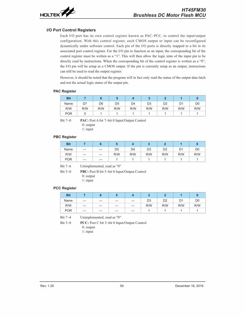
Rev. 1.20 50 De�e��e� 1�� 201� Rev. 1.20 51 De�e��e� 1�� 201�
HT45FM30Brushless DC Motor Flash MCU
I/O Port Control RegistersEach I/Oporthas itsowncontrol registerknownasPAC~PCC, to control the input/outputconfiguration.With this control register, eachCMOSoutput or input canbe reconfigureddynamicallyundersoftwarecontrol.Eachpinof theI/Oports isdirectlymappedtoabit in itsassociatedportcontrolregister.FortheI/Opintofunctionasaninput,thecorrespondingbitofthecontrolregistermustbewrittenasa“1”.Thiswillthenallowthelogicstateoftheinputpintobedirectlyreadbyinstructions.Whenthecorrespondingbitofthecontrolregisteriswrittenasa“0”,theI/OpinwillbesetupasaCMOSoutput.Ifthepiniscurrentlysetupasanoutput,instructionscanstillbeusedtoreadtheoutputregister.
However,itshouldbenotedthattheprogramwillinfactonlyreadthestatusoftheoutputdatalatchandnottheactuallogicstatusoftheoutputpin.
PAC Register
Bit 7 6 5 4 3 2 1 0Na�e D7 D� D5 D4 D3 D2 D1 D0R/W R/W R/W R/W R/W R/W R/W R/W R/WPOR 0 1 1 1 1 1 1 1
Bit7~0 PAC:PortAbit7~bit0Input/OutputControl0:output1:input
PBC Register
Bit 7 6 5 4 3 2 1 0Na�e — — D5 D4 D3 D2 D1 D0R/W — — R/W R/W R/W R/W R/W R/WPOR — — 1 1 1 1 1 1
Bit7~6 Unimplemented,readas"0"Bit5~0 PBC:PortBbit5~bit0Input/OutputControl
0:output1:input
PCC Register
Bit 7 6 5 4 3 2 1 0Na�e — — — — D3 D2 D1 D0R/W — — — — R/W R/W R/W R/WPOR — — — — 1 1 1 1
Bit7~4 Unimplemented,readas"0"Bit3~0 PCC:PortCbit3~bit0Input/OutputControl
0:output1:input
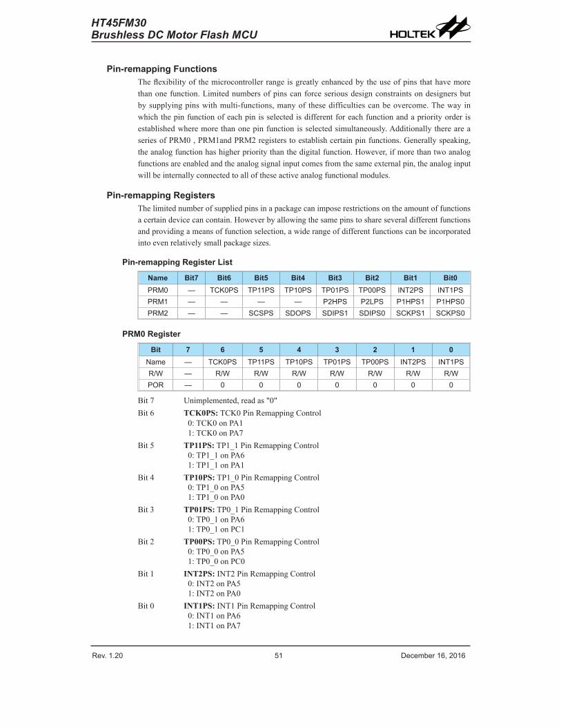
Rev. 1.20 50 De�e��e� 1�� 201� Rev. 1.20 51 De�e��e� 1�� 201�
HT45FM30Brushless DC Motor Flash MCU
Pin-remapping FunctionsTheflexibilityofthemicrocontrollerrangeisgreatlyenhancedbytheuseofpinsthathavemorethanonefunction.Limitednumbersofpinscanforceseriousdesignconstraintsondesignersbutbysupplyingpinswithmulti-functions,manyof thesedifficultiescanbeovercome.Thewayinwhichthepinfunctionofeachpinisselectedisdifferentforeachfunctionandapriorityorderisestablishedwheremorethanonepinfunctionisselectedsimultaneously.AdditionallythereareaseriesofPRM0,PRM1andPRM2registerstoestablishcertainpinfunctions.Generallyspeaking,theanalogfunctionhashigherprioritythanthedigitalfunction.However,ifmorethantwoanalogfunctionsareenabledandtheanalogsignalinputcomesfromthesameexternalpin,theanaloginputwillbeinternallyconnectedtoalloftheseactiveanalogfunctionalmodules.
Pin-remapping RegistersThelimitednumberofsuppliedpinsinapackagecanimposerestrictionsontheamountoffunctionsacertaindevicecancontain.Howeverbyallowingthesamepinstoshareseveraldifferentfunctionsandprovidingameansoffunctionselection,awiderangeofdifferentfunctionscanbeincorporatedintoevenrelativelysmallpackagesizes.
Pin-remapping Register List
Name Bit7 Bit6 Bit5 Bit4 Bit3 Bit2 Bit1 Bit0PRM0 — TCK0PS TP11PS TP10PS TP01PS TP00PS INT2PS INT1PSPRM1 — — — — P2HPS P2LPS P1HPS1 P1HPS0PRM2 — — SCSPS SDOPS SDIPS1 SDIPS0 SCKPS1 SCKPS0
PRM0 Register
Bit 7 6 5 4 3 2 1 0Na�e — TCK0PS TP11PS TP10PS TP01PS TP00PS INT2PS INT1PSR/W — R/W R/W R/W R/W R/W R/W R/WPOR — 0 0 0 0 0 0 0
Bit7 Unimplemented,readas"0"Bit6 TCK0PS:TCK0PinRemappingControl
0:TCK0onPA11:TCK0onPA7
Bit5 TP11PS:TP1_1PinRemappingControl0:TP1_1onPA61:TP1_1onPA1
Bit4 TP10PS:TP1_0PinRemappingControl0:TP1_0onPA51:TP1_0onPA0
Bit3 TP01PS:TP0_1PinRemappingControl0:TP0_1onPA61:TP0_1onPC1
Bit2 TP00PS:TP0_0PinRemappingControl0:TP0_0onPA51:TP0_0onPC0
Bit1 INT2PS:INT2PinRemappingControl0:INT2onPA51:INT2onPA0
Bit0 INT1PS:INT1PinRemappingControl0:INT1onPA61:INT1onPA7
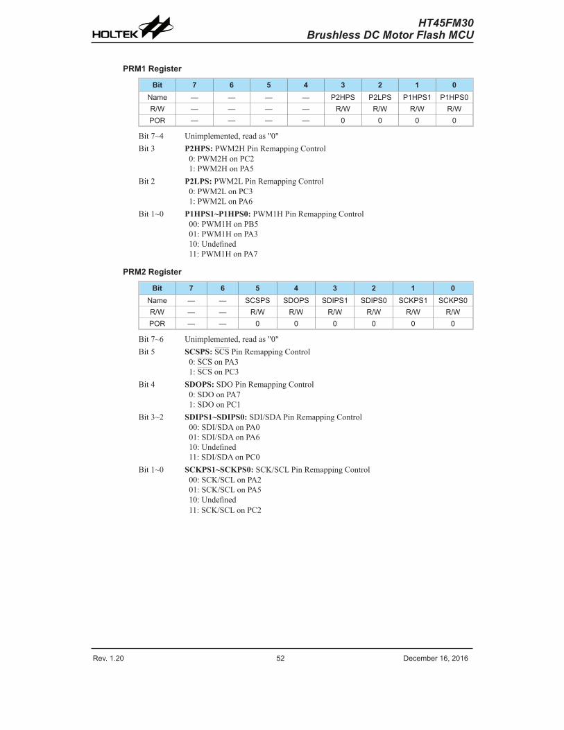
Rev. 1.20 52 De�e��e� 1�� 201� Rev. 1.20 53 De�e��e� 1�� 201�
HT45FM30Brushless DC Motor Flash MCU
PRM1 Register
Bit 7 6 5 4 3 2 1 0Na�e — — — — P2HPS P2LPS P1HPS1 P1HPS0R/W — — — — R/W R/W R/W R/WPOR — — — — 0 0 0 0
Bit7~4 Unimplemented,readas"0"Bit3 P2HPS:PWM2HPinRemappingControl
0:PWM2HonPC21:PWM2HonPA5
Bit2 P2LPS:PWM2LPinRemappingControl0:PWM2LonPC31:PWM2LonPA6
Bit1~0 P1HPS1~P1HPS0:PWM1HPinRemappingControl00:PWM1HonPB501:PWM1HonPA310:Undefined11:PWM1HonPA7
PRM2 Register
Bit 7 6 5 4 3 2 1 0Na�e — — SCSPS SDOPS SDIPS1 SDIPS0 SCKPS1 SCKPS0R/W — — R/W R/W R/W R/W R/W R/WPOR — — 0 0 0 0 0 0
Bit7~6 Unimplemented,readas"0"Bit5 SCSPS:SCSPinRemappingControl
0:SCSonPA31:SCSonPC3
Bit4 SDOPS:SDOPinRemappingControl0:SDOonPA71:SDOonPC1
Bit3~2 SDIPS1~SDIPS0:SDI/SDAPinRemappingControl00:SDI/SDAonPA001:SDI/SDAonPA610:Undefined11:SDI/SDAonPC0
Bit1~0 SCKPS1~SCKPS0:SCK/SCLPinRemappingControl00:SCK/SCLonPA201:SCK/SCLonPA510:Undefined11:SCK/SCLonPC2
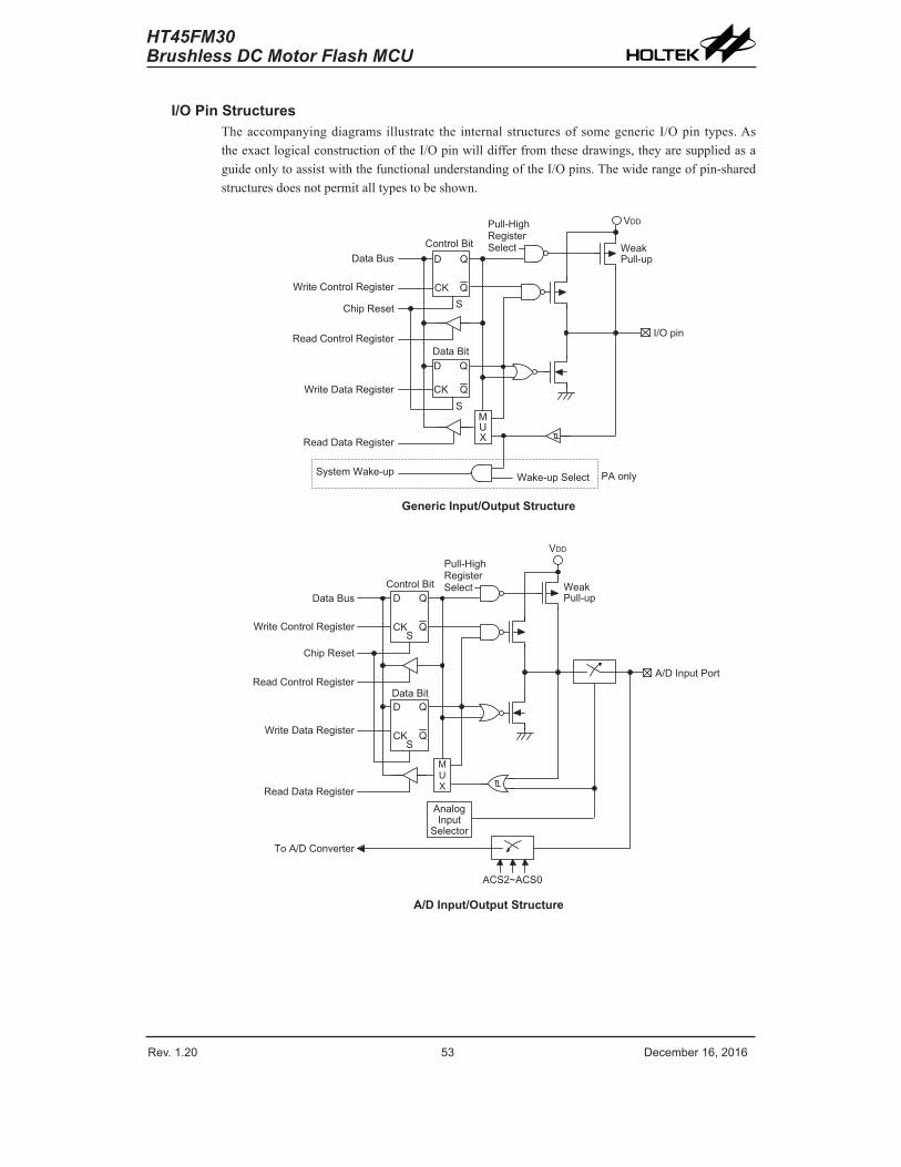
Rev. 1.20 52 De�e��e� 1�� 201� Rev. 1.20 53 De�e��e� 1�� 201�
HT45FM30Brushless DC Motor Flash MCU
I/O Pin StructuresTheaccompanyingdiagrams illustrate the internalstructuresofsomegeneric I/Opin types.AstheexactlogicalconstructionoftheI/Opinwilldifferfromthesedrawings,theyaresuppliedasaguideonlytoassistwiththefunctionalunderstandingoftheI/Opins.Thewiderangeofpin-sharedstructuresdoesnotpermitalltypestobeshown.
� � �
���
� � � � � � � � � � � � � �� � � � � � � � � � � � �
� � � � � � � � � � � � � � �
� �
� ��
� �
� ��
� � � � � � � � � � �� � � � � � �
� � � � � � � � � � � � � � � � � � � �
� � � � � � � � �
� � � � � � � � � � � � � � � � � �
� � � � � � � � � � � � � � � � �
� � � � � � � �
� � � � � � �
�
�
� � � � � � �
� � � �� � � � � � �
� � � � � � �� � � � � �� � � � � �
Generic Input/Output Structure
� � �
���� � � � � � � � � � � � � � � � � �
� � � � � � � � � �� � � � � � � �
� � � � � � � � � � � � � � � � � � � �
� � � � � � � � �
� � � � � � � � � � � � � � � � � � � �
� � � � � � � � � � � � � � � � � �
� � � � � � � �
� � � � � � � � � � � � � �
� � � � � � � � �
� � � � � � � � � � � � � � � �
� � �� � � � �
� � � � �� � � � �
� � � � � � �
�
� �
�
� �
� � � � � � � � � � � � � �� � � � �
A/D Input/Output Structure
Rev. 1.20 54 De�e��e� 1�� 201� Rev. 1.20 55 De�e��e� 1�� 201�
HT45FM30Brushless DC Motor Flash MCU
Programming ConsiderationsWithintheuserprogram,oneofthefirstthingstoconsiderisportinitialisation.Afterareset,alloftheI/Odataandportcontrolregisterswillbesethigh.ThismeansthatallI/Opinswilldefaulttoaninputstate, thelevelofwhichdependsontheotherconnectedcircuitryandwhetherpull-highselectionshavebeenchosen.Iftheportcontrolregisters,PAC~PCC,arethenprogrammedtosetupsomepinsasoutputs,theseoutputpinswillhaveaninitialhighoutputvalueunlesstheassociatedportdataregisters,PA~PC,arefirstprogrammed.Selectingwhichpinsare inputsandwhichareoutputscanbeachievedbyte-widebyloadingthecorrectvaluesintotheappropriateportcontrolregisterorbyprogrammingindividualbits intheportcontrolregisterusingthe“SET[m].i”and“CLR[m].i”instructions.Notethatwhenusingthesebitcontrolinstructions,aread-modify-writeoperationtakesplace.Themicrocontrollermustfirstreadinthedataontheentireport,modifyittotherequirednewbitvaluesandthenrewritethisdatabacktotheoutputports.
PortAhas theadditionalcapabilityofprovidingwake-upfunctions.When thedevice is in theSLEEPorIDLEMode,variousmethodsareavailabletowakethedeviceup.OneoftheseisahightolowtransitionofanyofthePortApins.SingleormultiplepinsonPortAcanbesetuptohavethisfunction.
Timer Modules – TMOneofthemostfundamentalfunctionsinanymicrocontrollerdeviceistheabilitytocontrolandmeasuretime.Toimplement timerelatedfunctionseachdeviceincludesseveralTimerModules,abbreviated to thenameTM.TheTMsaremulti-purpose timingunits and serve toprovideoperationssuchasTimer/Counter,InputCapture,CompareMatchOutputandSinglePulseOutputaswellasbeingthefunctionalunitforthegenerationofPWMsignals.EachoftheTMshaseithertwoindividualinterrupts.TheadditionofinputandoutputpinsforeachTMensuresthatusersareprovidedwithtimingunitswithawideandflexiblerangeoffeatures.ThecommonfeaturesofthedifferentTMtypesaredescribedherewithmoredetailedinformationprovidedintheindividualCompactandStandardsections.
Introduction Thedevicecontainsa16-bitCompactTypeanda10-bitStandardTypeTMunitwhicharewiththeirindividualreferencename,TM0andTM1.Althoughsimilarinnature,thedifferentTMtypesvaryintheirfeaturecomplexity.Thecommonfeatures tobothofCompactandStandardTMswillbedescribedinthissection,thedetailedoperationregardingeachoftheTMtypeswillbedescribedinseparatesections.ThemainfeaturesanddifferencesbetweenthetwotypesofTMsaresummarisedintheaccompanyingtable.
Function CTM STMTi�e�/Counte� √ √I/P Captu�e ― √Co�pa�e Mat�h Output √ √PWM Channels 1 1Single Pulse Output ― 1PWM Align�ent Edge EdgePWM Adjust�ent Pe�iod & Duty Duty o� Pe�iod Duty o� Pe�iod
TM Function Summary
Rev. 1.20 54 De�e��e� 1�� 201� Rev. 1.20 55 De�e��e� 1�� 201�
HT45FM30Brushless DC Motor Flash MCU
TM OperationThetwodifferent typesofTMofferadiverserangeoffunctions,fromsimpletimingoperationstoPWMsignalgeneration.ThekeytounderstandinghowtheTMoperatesistoseeitintermsofafreerunningcounterwhosevalueis thencomparedwiththevalueofpre-programmedinternalcomparators.Whenthefreerunningcounterhasthesamevalueasthepre-programmedcomparator,knownasacomparematchsituation,aTMinterruptsignalwillbegeneratedwhichcanclearthecounterandperhapsalsochangetheconditionoftheTMoutputpin.TheinternalTMcounter isdrivenbyauserselectableclocksource,whichcanbeaninternalclockoranexternalpin.
TM Clock SourceTheclocksourcewhichdrives themaincounter ineachTMcanoriginatefromvarioussources.TheselectionoftherequiredclocksourceisimplementedusingtheTnCK2~TnCK0bitsintheTMcontrolregisters.TheclocksourcecanbearatioofeitherthesystemclockfSYSortheinternalhighclockfH,thefTBCclocksourceortheexternalTCKnpin.Notethatsettingthesebitstothevalue101willselectareservedclockinput,ineffectdisconnectingtheTMclocksource.TheTCKnpinclocksourceisusedtoallowanexternalsignaltodrivetheTMasanexternalclocksourceorforeventcounting.
TM InterruptsTheCompactandStandardtypeTMseachhavetwointernalinterrupts,oneforeachoftheinternalcomparatorAorcomparatorP,whichgenerateaTMinterruptwhenacomparematchconditionoccurs.
TM External PinsEachoftheTMs,irrespectiveofwhattype,hasoneTMinputpin,withthelabelTCKn.TheTMinputpin,isessentiallyaclocksourcefortheTMandisselectedusingtheTnCK2~TnCK0bitsintheTMnC0register.ThisexternalTMinputpinallowsanexternalclocksourcetodrivetheinternalTM.ThisexternalTMinputpinissharedwithotherfunctionsbutwillbeconnectedtotheinternalTMifselectedusingtheTnCK2~TnCK0bits.TheTMinputpincanbechosentohaveeitherarisingorfallingactiveedge.TheTMseachhaveoneormoreoutputpinswiththelabelTPn.WhentheTMisintheCompareMatchOutputMode,thesepinscanbecontrolledbytheTMtoswitchtoahighorlowlevelortotogglewhenacomparematchsituationoccurs.TheexternalTPnoutputpinisalsothepinwheretheTMgeneratesthePWMoutputwaveform.AstheTMoutputpinsarepin-sharedwithotherfunction,theTMoutputfunctionmustfirstbesetupusingregisters.Asinglebit inoneof theregistersdeterminesif itsassociatedpinis tobeusedasanexternalTMoutputpinorifitistohaveanotherfunction.ThenumberofoutputpinsforeachTMtypeanddeviceisdifferent,thedetailsareprovidedintheaccompanyingtable.
Rev. 1.20 5� De�e��e� 1�� 201� Rev. 1.20 57 De�e��e� 1�� 201�
HT45FM30Brushless DC Motor Flash MCU
TM Input/Output Pin Control Registers
� � � � � � � � �
� � �� � � � �
� � � � � � � �
� � � � � � � � � � � � � � � � � � � � � � � � �
�
� � � � � � � � � �
�
� � � � � �
� � � � � � � � � � �� � � � � � � �
� � � � �
� � � � � � � � � � � � � � � � � � � � � � � � �
�
� � � � � � � � � �
�
�
� � � � � � � � � � �� � � � � � � �
� � � � �
� � � � � � � � �
� � �� � � � �
� � � � � � � �
� � � � � � � � � � � � � � � � � � � � � � � � � �
�
�
�� � � � � �
� � � � �
� � � � � � � � � � � � � � � � � � � � � � � � �
�
� � � � � � � � �
�
�
� � � � � � � � � � �� � � � � � �
� � � � �
�
�
� � � � �
�
�
� � � � �
� � � � � � � � � � � � �
� � � � � � � � � � �� � � � � � � �
� � � � � � � � �
SelectingtohaveaTMinput/outputorwhethertoretainitsothersharedfunction,isimplementedusingoneortworegisters,withasinglebitineachregistercorrespondingtoaTMinput/outputpin.SettingthebithighwillsetupthecorrespondingpinasaTMinput/output, ifresettozerothepinwillretainitsoriginalotherfunction.
Rev. 1.20 5� De�e��e� 1�� 201� Rev. 1.20 57 De�e��e� 1�� 201�
HT45FM30Brushless DC Motor Flash MCU
TMPC0 Register
Bit 7 6 5 4 3 2 1 0Na�e — — T1CP1 T1CP0 — — T0CP1 T0CP0R/W — — R/W R/W — — R/W R/WPOR — — 0 1 — — 0 1
Bit7~6 Unimplemented,readas"0"Bit5 T1CP1:TP1_1pinControl
0:disable1:enable
Bit4 T1CP0:TP1_0pinControl0:disable1:enable
Bit3~2 Unimplemented,readas"0"Bit1 T0CP1:TP0_1pinControl
0:disable1:enable
Bit0 T0CP0:TP0_0pinControl0:disable1:enable
Programming ConsiderationsTheTMCounterRegistersandtheCapture/CompareCCRAregister,beingeither10-bitor16-bit,allhavealowandhighbytestructure.Thehighbytescanbedirectlyaccessed,butasthelowbytescanonlybeaccessedviaaninternal8-bitbuffer,readingorwritingtotheseregisterpairsmustbecarriedoutinaspecificway.Theimportantpointtonoteisthatdatatransfertoandfromthe8-bitbufferanditsrelatedlowbyteonlytakesplacewhenawriteorreadoperationtoitscorrespondinghighbyteisexecuted.
� � � � � � � � � � � � � � � � � � � � � � � � � � � � � �
� � � � � � �
� � � � � � � � �
� � � � � � � � � � � �
� � �� � �� � � � � � � � � � � � � � � � � � � � � � � � � � � � �
Thefollowingstepsshowthereadandwriteprocedures:
• WritingDatatoCCRA♦ Step1.WritedatatoLowByteTMxAL
– notethatheredataisonlywrittentothe8-bitbuffer.♦ Step2.WritedatatoHighByteTMxAH
– heredataiswrittendirectlytothehighbyteregistersandsimultaneouslydataislatchedfromthe8-bitbuffertotheLowByteregisters.
• ReadingDatafromtheCounterRegistersandCCRA♦ Step1.ReaddatafromtheHighByteTMxDHorTMxAH
– heredataisreaddirectlyfromtheHighByteregistersandsimultaneouslydataislatchedfromtheLowByteregisterintothe8-bitbuffer.
♦ Step2.ReaddatafromtheLowByteTMxDLorTMxAL– thisstepreadsdatafromthe8-bitbuffer.
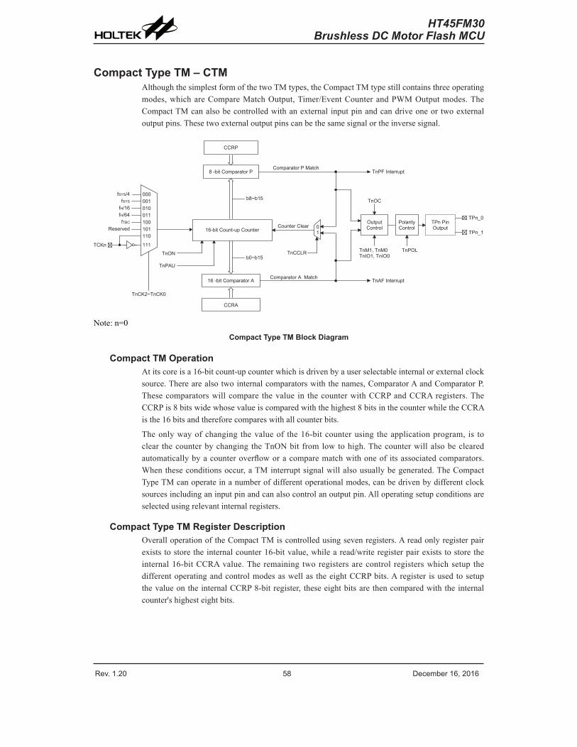
Rev. 1.20 58 De�e��e� 1�� 201� Rev. 1.20 59 De�e��e� 1�� 201�
HT45FM30Brushless DC Motor Flash MCU
Compact Type TM – CTMAlthoughthesimplestformofthetwoTMtypes,theCompactTMtypestillcontainsthreeoperatingmodes,whichareCompareMatchOutput,Timer/EventCounterandPWMOutputmodes.TheCompactTMcanalsobecontrolledwithanexternalinputpinandcandriveoneortwoexternaloutputpins.Thesetwoexternaloutputpinscanbethesamesignalortheinversesignal.
� � � �
� � � �
� � � � � �
� � � � � � � � � � � � � � � � � �
� � � � � � � � � � � � � � � � � � �
� � � � � � � � � �
� �
� � � � �
� � � � � �
� � � � � � � � � � � � � � � � � � �
� � � �
� � � � � � � � � � � � � � � � � � � �
� � � � � � � � � � � � �� � � � � � � � � � � � � � � � � � � � � � �
� � � � � � � � � � � � � �
� � � � � � � � � � � � � �
� � � � � � � � � � � �
� � � � � � �� � � � � � � � � �� � � � � � � � � �
� � � �
� � �
� � � � � � � � � � � � � �
� � � � �� � � � � � �
� � � �
� � � �
� � �
� � �� � �� � �� � �� � �� � �� � �
� � � � � �� � � �� � � � �� � � � �� � � �
� � � � � � � � ��
Note:n=0
Compact Type TM Block Diagram
Compact TM OperationAtitscoreisa16-bitcount-upcounterwhichisdrivenbyauserselectableinternalorexternalclocksource.Therearealsotwointernalcomparatorswiththenames,ComparatorAandComparatorP.Thesecomparatorswillcompare thevalue in thecounterwithCCRPandCCRAregisters.TheCCRPis8bitswidewhosevalueiscomparedwiththehighest8bitsinthecounterwhiletheCCRAisthe16bitsandthereforecompareswithallcounterbits.
Theonlywayofchanging thevalueof the16-bitcounterusing theapplicationprogram, is toclear thecounterbychanging theTnONbit fromlowtohigh.Thecounterwillalsobeclearedautomaticallybyacounteroverfloworacomparematchwithoneof itsassociatedcomparators.Whentheseconditionsoccur,aTMinterruptsignalwillalsousuallybegenerated.TheCompactTypeTMcanoperateinanumberofdifferentoperationalmodes,canbedrivenbydifferentclocksourcesincludinganinputpinandcanalsocontrolanoutputpin.Alloperatingsetupconditionsareselectedusingrelevantinternalregisters.
Compact Type TM Register DescriptionOveralloperationoftheCompactTMiscontrolledusingsevenregisters.Areadonlyregisterpairexiststostoretheinternalcounter16-bitvalue,whilearead/writeregisterpairexiststostoretheinternal16-bitCCRAvalue.Theremaining tworegistersarecontrol registerswhichsetup thedifferentoperatingandcontrolmodesaswellas theeightCCRPbits.Aregister isusedtosetupthevalueontheinternalCCRP8-bitregister, theseeightbitsarethencomparedwiththeinternalcounter'shighesteightbits.
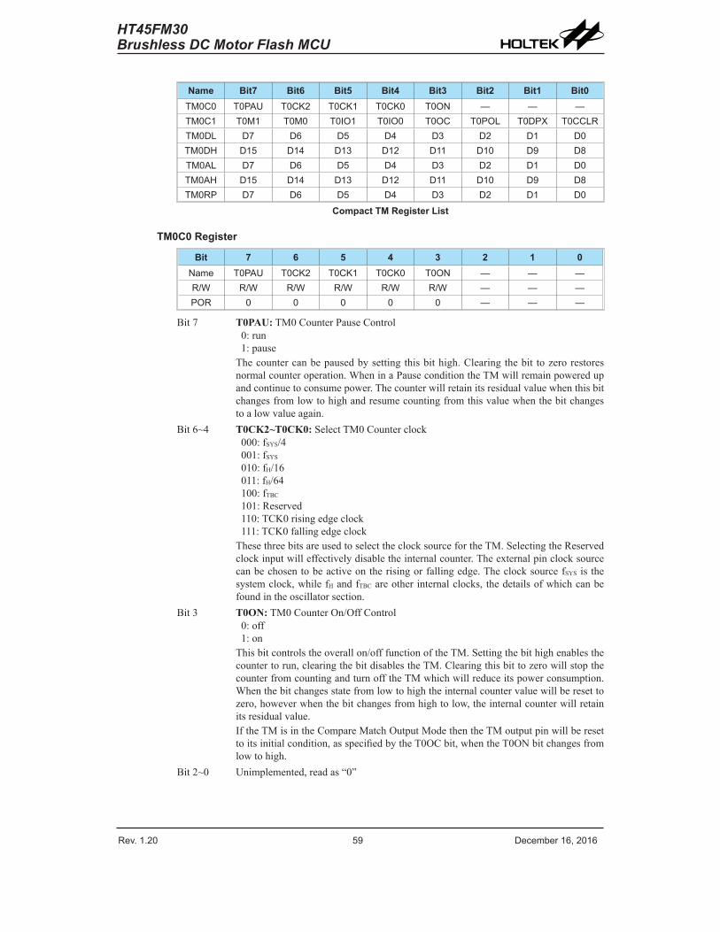
Rev. 1.20 58 De�e��e� 1�� 201� Rev. 1.20 59 De�e��e� 1�� 201�
HT45FM30Brushless DC Motor Flash MCU
Name Bit7 Bit6 Bit5 Bit4 Bit3 Bit2 Bit1 Bit0TM0C0 T0PAU T0CK2 T0CK1 T0CK0 T0ON — — —TM0C1 T0M1 T0M0 T0IO1 T0IO0 T0OC T0POL T0DPX T0CCLRTM0DL D7 D� D5 D4 D3 D2 D1 D0TM0DH D15 D14 D13 D12 D11 D10 D9 D8TM0AL D7 D� D5 D4 D3 D2 D1 D0TM0AH D15 D14 D13 D12 D11 D10 D9 D8TM0RP D7 D� D5 D4 D3 D2 D1 D0
Compact TM Register List
TM0C0 Register
Bit 7 6 5 4 3 2 1 0Na�e T0PAU T0CK2 T0CK1 T0CK0 T0ON — — —R/W R/W R/W R/W R/W R/W — — —POR 0 0 0 0 0 — — —
Bit7 T0PAU:TM0CounterPauseControl0:run1:pauseThecountercanbepausedbysettingthisbithigh.Clearingthebit tozerorestoresnormalcounteroperation.WheninaPauseconditiontheTMwillremainpoweredupandcontinuetoconsumepower.Thecounterwillretainitsresidualvaluewhenthisbitchangesfromlowtohighandresumecountingfromthisvaluewhenthebitchangestoalowvalueagain.
Bit6~4 T0CK2~T0CK0:SelectTM0Counterclock000:fSYS/4001:fSYS010:fH/16011:fH/64100:fTBC101:Reserved110:TCK0risingedgeclock111:TCK0fallingedgeclockThesethreebitsareusedtoselecttheclocksourcefortheTM.SelectingtheReservedclockinputwilleffectivelydisabletheinternalcounter.Theexternalpinclocksourcecanbechosentobeactiveontherisingorfallingedge.TheclocksourcefSYS isthesystemclock,whilefHandfTBCareotherinternalclocks,thedetailsofwhichcanbefoundintheoscillatorsection.
Bit3 T0ON:TM0CounterOn/OffControl0:off1:onThisbitcontrolstheoverallon/offfunctionoftheTM.Settingthebithighenablesthecountertorun,clearingthebitdisablestheTM.ClearingthisbittozerowillstopthecounterfromcountingandturnofftheTMwhichwillreduceitspowerconsumption.Whenthebitchangesstatefromlowtohightheinternalcountervaluewillberesettozero,howeverwhenthebitchangesfromhightolow,theinternalcounterwillretainitsresidualvalue.IftheTMisintheCompareMatchOutputModethentheTMoutputpinwillberesettoitsinitialcondition,asspecifiedbytheT0OCbit,whentheT0ONbitchangesfromlowtohigh.
Bit2~0 Unimplemented,readas“0”
Rev. 1.20 �0 De�e��e� 1�� 201� Rev. 1.20 �1 De�e��e� 1�� 201�
HT45FM30Brushless DC Motor Flash MCU
TM0C1 Register
Bit 7 6 5 4 3 2 1 0Na�e T0M1 T0M0 T0IO1 T0IO0 T0OC T0POL T0DPX T0CCLRR/W R/W R/W R/W R/W R/W R/W R/W R/WPOR 0 0 0 0 0 0 0 0
Bit7~6 T0M1~T0M0:SelectTM0OperatingMode00:CompareMatchOutputMode01:UndefinedMode10:PWMMode11:Timer/CounterModeThesebitssetuptherequiredoperatingmodefortheTM.ToensurereliableoperationtheTMshouldbeswitchedoffbeforeanychangesaremadetotheT0M1andT0M0bits.IntheTimer/CounterMode,theTMoutputpincontrolmustbedisabled.
Bit5~4 T0IO1~T0IO0:SelectTP0_0,TP0_1outputfunctionCompareMatchOutputMode00:nochange01:outputlow10:outputhigh11:toggleoutputPWMMode00:forceinactivestate01:forceactivestate10:PWMoutput11:undefinedTimer/counterMode:unusedThesetwobitsareusedtodeterminehowtheTMoutputpinchangesstatewhenacertainconditionisreached.ThefunctionthatthesebitsselectdependsuponinwhichmodetheTMisrunning.IntheCompareMatchOutputMode,theT0IO1andT0IO0bitsdeterminehowtheTMoutputpinchangesstatewhenacomparematchoccursfromtheComparatorA.TheTMoutputpincanbesetuptoswitchhigh,switchlowor totoggleitspresentstatewhenacomparematchoccursfromtheComparatorA.Whenthebitsarebothzero,thennochangewilltakeplaceontheoutput.TheinitialvalueoftheTMoutputpinshouldbesetupusingtheT0OCbit intheTM0C1register.NotethattheoutputlevelrequestedbytheT0IO1andT0IO0bitsmustbedifferentfromtheinitialvaluesetupusingtheT0OCbitotherwisenochangewilloccurontheTMoutputpinwhenacomparematchoccurs.AftertheTMoutputpinchangesstateitcanberesettoitsinitiallevelbychangingtheleveloftheT0ONbitfromlowtohigh.
Bit3 T0OC:TP0_0,TP0_1OutputcontrolbitCompareMatchOutputMode0:initiallow1:initialhighPWMMode0:activelow1:activehighThis is theoutputcontrolbit for theTMoutputpin. ItsoperationdependsuponwhetherTMisbeingusedintheCompareMatchOutputModeorinthePWMMode.IthasnoeffectiftheTMisintheTimer/CounterMode.IntheCompareMatchOutputMode itdetermines the logic levelof theTMoutputpinbeforeacomparematchoccurs.InthePWMModeitdeterminesif thePWMsignal isactivehighoractivelow.
Rev. 1.20 �0 De�e��e� 1�� 201� Rev. 1.20 �1 De�e��e� 1�� 201�
HT45FM30Brushless DC Motor Flash MCU
Bit2 T0POL:TP0_0,TP0_1OutputpolarityControl0:non-invert1:invertThisbitcontrolsthepolarityoftheTP0_0orTP0_1outputpin.Whenthebit issethightheTMoutputpinwillbeinvertedandnotinvertedwhenthebitiszero.IthasnoeffectiftheTMisintheTimer/CounterMode.
Bit1 T0DPX:TM0PWMperiod/dutyControl0:CCRP–period;CCRA–duty1:CCRP–duty;CCRA–periodThisbit,determineswhichoftheCCRAandCCRPregistersareusedforperiodanddutycontrolofthePWMwaveform.
Bit0 T0CCLR:SelectTM0Counterclearcondition0:TM0ComparatorPmatch1:TM0ComparatorAmatchThisbit isused toselect themethodwhichclears thecounter.Remember that theCompactTMcontainstwocomparators,ComparatorAandComparatorP,eitherofwhichcanbeselectedtoclear the internalcounter.With theT0CCLRbitsethigh,thecounterwillbeclearedwhenacomparematchoccursfromtheComparatorA.Whenthebitislow,thecounterwillbeclearedwhenacomparematchoccursfromtheComparatorPorwithacounteroverflow.AcounteroverflowclearingmethodcanonlybeimplementediftheCCRPbitsareallclearedtozero.TheT0CCLRbitisnotusedinthePWMMode.
TM0DL Register
Bit 7 6 5 4 3 2 1 0Na�e D7 D� D5 D4 D3 D2 D1 D0R/W R R R R R R R RPOR 0 0 0 0 0 0 0 0
Bit7~0 TM0DL:TM0CounterLowByteRegisterbit7~bit0TM016-bitCounterbit7~bit0
TM0DH Register
Bit 7 6 5 4 3 2 1 0Na�e D15 D14 D13 D12 D11 D10 D9 D8R/W R/W R/W R/W R/W R/W R/W R RPOR 0 0 0 0 0 0 0 0
Bit7~0 TM0DH:TM0CounterHighByteRegisterbit7~bit0TM016-bitCounterbit15~bit8
TM0AL Register
Bit 7 6 5 4 3 2 1 0Na�e D7 D� D5 D4 D3 D2 D1 D0R/W R/W R/W R/W R/W R/W R/W R/W R/WPOR 0 0 0 0 0 0 0 0
Bit7~0 TM0AL:TM0CCRALowByteRegisterbit7~bit0TM016-bitCCRAbit7~bit0
Rev. 1.20 �2 De�e��e� 1�� 201� Rev. 1.20 �3 De�e��e� 1�� 201�
HT45FM30Brushless DC Motor Flash MCU
TM0AH Register
Bit 7 6 5 4 3 2 1 0Na�e D15 D14 D13 D12 D11 D10 D9 D8R/W R/W R/W R/W R/W R/W R/W R/W R/WPOR 0 0 0 0 0 0 0 0
Bit7~0 TM0AH:TM0CCRAHighByteRegisterbit7~bit0TM016-bitCCRAbit15~bit8
TM0RP Register
Bit 7 6 5 4 3 2 1 0Na�e D7 D� D5 D4 D3 D2 D1 D0R/W R/W R/W R/W R/W R/W R/W R/W R/WPOR 0 0 0 0 0 0 0 0
Bit7~0 TM0RP:TM0CCRPRegisterbit7~bit0TM0CCRP8-bitregister,comparedwiththeTM0Counterbit15~bit8.ComparatorPMatchPeriod0:65536TM0clocks1~255:256×1~255TM0clocksTheseeightbitsareusedtosetupthevalueontheinternalCCRP8-bitregister,whichare thencomparedwith the internalcounter'shighesteightbits.Theresultof thiscomparisoncanbeselectedtoclear theinternalcounterif theT0CCLRbit isset tozero.SettingtheT0CCLRbit tozeroensuresthatacomparematchwiththeCCRPvalueswillreset theinternalcounter.AstheCCRPbitsareonlycomparedwiththehighesteightcounterbits, thecomparevaluesexist in256clockcyclemultiples.Clearingalleightbits tozero is ineffectallowing thecounter tooverflowat itsmaximumvalue.
Compact Type TM Operating ModesTheCompactTypeTMcanoperateinoneofthreeoperatingmodes,CompareMatchOutputMode,PWMModeorTimer/CounterMode.TheoperatingmodeisselectedusingtheT0M1andT0M0bitsintheTM0C1register.
Compare Match Output ModeToselectthismode,bitsT0M1andT0M0intheTM0C1register,shouldbesetto“00”respectively.Inthismodeoncethecounterisenabledandrunningitcanbeclearedbythreemethods.Theseareacounteroverflow,acomparematchfromComparatorAandacomparematchfromComparatorP.WhentheT0CCLRbitislow,therearetwowaysinwhichthecountercanbecleared.OneiswhenacomparematchoccursfromComparatorP, theotheriswhentheCCRPbitsareallzerowhichallowsthecountertooverflow.HerebothT0AFandT0PFinterruptrequestflagsfortheComparatorAandComparatorPrespectively,willbothbegenerated.
IftheT0CCLRbitintheTM0C1registerishighthenthecounterwillbeclearedwhenacomparematchoccurs fromComparatorA.However,hereonly theT0AFinterrupt request flagwillbegeneratedevenifthevalueoftheCCRPbitsislessthanthatoftheCCRAregisters.ThereforewhenT0CCLRishighnoT0PFinterruptrequestflagwillbegenerated.IftheCCRAbitsareallzero,thecounterwilloverflowwhenitsreachesitsmaximum16-bit,FFFFHex,value,howeverheretheT0AFinterruptrequestflagwillnotbegenerated.
Rev. 1.20 �2 De�e��e� 1�� 201� Rev. 1.20 �3 De�e��e� 1�� 201�
HT45FM30Brushless DC Motor Flash MCU
Asthenameof themodesuggests,afteracomparison ismade, theTMoutputpinwillchangestate.TheTMoutputpinconditionhoweveronlychangesstatewhenaT0AFinterruptrequestflagisgeneratedafteracomparematchoccursfromComparatorA.TheT0PFinterruptrequestflag,generatedfromacomparematchoccursfromComparatorP,willhavenoeffectontheTMoutputpin.Thewayinwhich theTMoutputpinchangesstatearedeterminedby theconditionof theT0IO1andT0IO0bitsintheTM0C1register.TheTMoutputpincanbeselectedusingtheT0IO1andT0IO0bitstogohigh,togolowortotogglefromitspresentconditionwhenacomparematchoccursfromComparatorA.Theinitialconditionof theTMoutputpin,which issetupafter theT0ONbitchangesfromlowtohigh,issetupusingtheT0OCbit.NotethatiftheT0IO1andT0IO0bitsarezerothennopinchangewilltakeplace.
Counte� Value
0x3FF
CCRP
CCRA
TnON
TnPAU
TnPOL
CCRP Int. Flag TnPF
CCRA Int. Flag TnAF
TM O/P Pin
Ti�e
CCRP=0
CCRP > 0
Counte� ove�flowCCRP > 0Counte� �lea�ed �y CCRP value
Pause
Resu�e
Stop
Counte� Resta�t
TnCCLR = 0; TnM [1:0] = 00
Output pin set to initial Level Low if TnOC=0
Output Toggle with TnAF flag
Note TnIO [1:0] = 10 A�tive High Output sele�tHe�e TnIO [1:0] = 11
Toggle Output sele�t
Output not affe�ted �y TnAF flag. Re�ains High until �eset �y TnON �it
Output PinReset to Initial value
Output �ont�olled �y othe� pin-sha�ed fun�tion
Output Inve�tswhen TnPOL is high
Compare Match Output Mode – TnCCLR=0
Note:1.n=0
2.WithT0CCLR=0theComparatorPmatchwillclearthecounter
3.TMoutputpincontrolledonlybyT0AFflag
4.OutputpinresettoinitialstatebyT0ONbitrisingedge
Rev. 1.20 �4 De�e��e� 1�� 201� Rev. 1.20 �5 De�e��e� 1�� 201�
HT45FM30Brushless DC Motor Flash MCU
Counte� Value
0x3FF
CCRP
CCRA
TnON
TnPAU
TnPOL
CCRP Int. Flag TnPF
CCRA Int. Flag TnAF
TM O/P Pin
Ti�e
CCRA=0
CCRA = 0Counte� ove�flowCCRA > 0 Counte� �lea�ed �y CCRA value
Pause
Resu�e
Stop Counte� Resta�t
TnCCLR = 1; TnM [1:0] = 00
Output pin set to initial Level Low if TnOC=0
Output Toggle with TnAF flag
Note TnIO [1:0] = 10 A�tive High Output sele�tHe�e TnIO [1:0] = 11
Toggle Output sele�t
Output not affe�ted �y TnAF flag. Re�ains High until �eset �y TnON �it
Output PinReset to Initial value
Output �ont�olled �y othe� pin-sha�ed fun�tion
Output Inve�tswhen TnPOL is high
TnPF not gene�ated
No TnAF flag gene�ated on CCRA ove�flow
Output does not �hange
Compare Match Output Mode – TnCCLR=1
Note:1.WithT0CCLR=1theComparatorAmatchwillclearthecounter
2.TMoutputpincontrolledonlybyT0AFflag
3.TMoutputpinresettoinitialstatebyT0ONrisingedge
4.T0PFflagsnotgeneratedwhenT0CCLR=1
5.n=0
Rev. 1.20 �4 De�e��e� 1�� 201� Rev. 1.20 �5 De�e��e� 1�� 201�
HT45FM30Brushless DC Motor Flash MCU
Timer/Counter ModeToselectthismode,bitsT0M1andT0M0intheTM0C1registershouldbesetto11respectively.TheTimer/CounterModeoperates in an identicalway to theCompareMatchOutputModegeneratingthesameinterruptflags.TheexceptionisthatintheTimer/CounterModetheTMoutputpin isnotused.Therefore theabovedescriptionandTimingDiagramsfor theCompareMatchOutputModecanbeusedtounderstanditsfunction.AstheTMoutputpinisnotusedinthismode,thepincanbeusedasanormalI/Opinorotherpin-sharedfunction.
PWM Output ModeToselectthismode,bitsT0M1andT0M0intheTM0C1registershouldbesetto10respectively.ThePWMfunctionwithintheTMisusefulforapplicationswhichrequirefunctionssuchasmotorcontrol,heatingcontrol, illuminationcontroletc.Byprovidingasignalof fixedfrequencybutofvaryingdutycycleontheTMoutputpin,asquarewaveACwaveformcanbegeneratedwithvaryingequivalentDCRMSvalues.
AsboththeperiodanddutycycleofthePWMwaveformcanbecontrolled,thechoiceofgeneratedwaveformisextremelyflexible.In thePWMmode, theT0CCLRbithasnoeffectonthePWMoperation.Bothof theCCRAandCCRPregistersareusedtogeneratethePWMwaveform,oneregisterisusedtocleartheinternalcounterandthuscontrolthePWMwaveformfrequency,whiletheotheroneisusedtocontrol thedutycycle.Whichregister isusedtocontroleitherfrequencyordutycycle isdeterminedusing theT0DPXbit in theTM0C1register.ThePWMwaveformfrequencyanddutycyclecanthereforebecontrolledbythevaluesintheCCRAandCCRPregisters.
Aninterruptflag,oneforeachoftheCCRAandCCRP,willbegeneratedwhenacomparematchoccursfromeitherComparatorAorComparatorP.TheT0OCbitintheTM0C1registerisusedtoselecttherequiredpolarityofthePWMwaveformwhilethetwoT0IO1andT0IO0bitsareusedtoenablethePWMoutputortoforcetheTMoutputpintoafixedhighorlowlevel.TheT0POLbitisusedtoreversethepolarityofthePWMoutputwaveform.
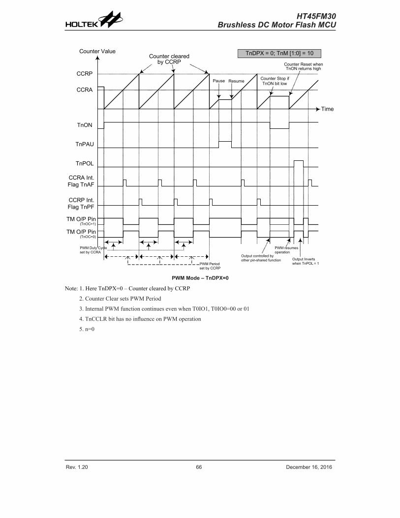
Rev. 1.20 �� De�e��e� 1�� 201� Rev. 1.20 �7 De�e��e� 1�� 201�
HT45FM30Brushless DC Motor Flash MCU
Counte� Value
CCRP
CCRA
TnON
TnPAU
TnPOL
CCRP Int. Flag TnPF
CCRA Int. Flag TnAF
TM O/P Pin(TnOC=1)
Ti�e
Counte� �lea�ed �y CCRP
Pause Resu�e Counte� Stop if TnON �it low
Counte� Reset when TnON �etu�ns high
TnDPX = 0; TnM [1:0] = 10
PWM Duty Cy�le set �y CCRA
PWM �esu�es ope�ation
Output �ont�olled �y othe� pin-sha�ed fun�tion Output Inve�ts
when TnPOL = 1PWM Pe�iod set �y CCRP
TM O/P Pin(TnOC=0)
PWM Mode – TnDPX=0
Note:1.HereTnDPX=0–CounterclearedbyCCRP
2.CounterClearsetsPWMPeriod
3.InternalPWMfunctioncontinuesevenwhenT0IO1,T0IO0=00or01
4.TnCCLRbithasnoinfluenceonPWMoperation
5.n=0
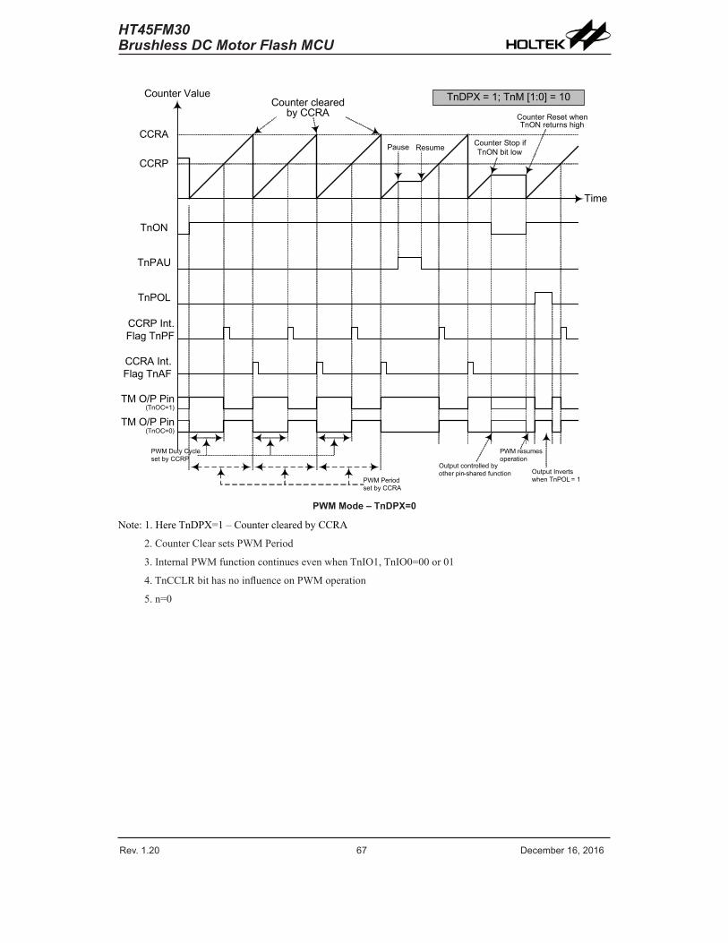
Rev. 1.20 �� De�e��e� 1�� 201� Rev. 1.20 �7 De�e��e� 1�� 201�
HT45FM30Brushless DC Motor Flash MCU
Counte� Value
CCRP
CCRA
TnON
TnPAU
TnPOL
CCRP Int. Flag TnPF
CCRA Int. Flag TnAF
TM O/P Pin(TnOC=1)
Ti�e
Counte� �lea�ed �y CCRA
Pause Resu�e Counte� Stop if TnON �it low
Counte� Reset when TnON �etu�ns high
TnDPX = 1; TnM [1:0] = 10
PWM Duty Cy�le set �y CCRP
PWM �esu�es ope�ation
Output �ont�olled �y othe� pin-sha�ed fun�tion Output Inve�ts
when TnPOL = 1PWM Pe�iod set �y CCRA
TM O/P Pin(TnOC=0)
PWM Mode – TnDPX=0
Note:1.HereTnDPX=1–CounterclearedbyCCRA
2.CounterClearsetsPWMPeriod
3.InternalPWMfunctioncontinuesevenwhenTnIO1,TnIO0=00or01
4.TnCCLRbithasnoinfluenceonPWMoperation
5.n=0
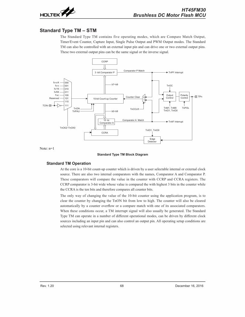
Rev. 1.20 �8 De�e��e� 1�� 201� Rev. 1.20 �9 De�e��e� 1�� 201�
HT45FM30Brushless DC Motor Flash MCU
Standard Type TM – STMTheStandardTypeTMcontains fiveoperatingmodes,which areCompareMatchOutput,Timer/EventCounter,CaptureInput,SinglePulseOutputandPWMOutputmodes.TheStandardTMcanalsobecontrolledwithanexternalinputpinandcandriveoneortwoexternaloutputpins.Thesetwoexternaloutputpinscanbethesamesignalortheinversesignal.
� � � �
� � � �
� � � � � �
� � � � � � � � � � � � � � � � � �
� � � � � � � � � � � � � � � � � � �
� � � � � � � � � �
� � � � � � �
� � � � �
� � � � � � � � � � � � � � � � � � �
� � � �
� � � � � �� � � � � � � � � � � � �
� � � � � � � � � � � � �� � � � � � � � � � � � � � � � � � � � � � �
� � � � � � � � � � � � � �
� � � � � � � � � � � � � �
� � � � � �� � � � � � � � � �� � � � � � � � � �
� � � �
� � �
� � � � � � � � � � � � � �
� � � � �� � � � � � � � � �
� � �
� � �� � �� � �� � �� � �� � �� � �
� � � � � � � � � � � � � � � � � � �
� � � � � � � � ��
� � � �� � � � � � � � � � �
� � � � � � � � � �
Note:n=1
Standard Type TM Block Diagram
Standard TM OperationAtthecoreisa10-bitcount-upcounterwhichisdrivenbyauserselectableinternalorexternalclocksource.Therearealsotwointernalcomparatorswiththenames,ComparatorAandComparatorP.Thesecomparatorswillcompare thevalue in thecounterwithCCRPandCCRAregisters.TheCCRPcomparatoris3-bitwidewhosevalueiscomparedthewithhighest3bitsinthecounterwhiletheCCRAisthetenbitsandthereforecomparesallcounterbits.
Theonlywayofchanging thevalueof the10-bitcounterusing theapplicationprogram, is toclear thecounterbychanging theTnONbit fromlowtohigh.Thecounterwillalsobeclearedautomaticallybyacounteroverfloworacomparematchwithoneof itsassociatedcomparators.Whentheseconditionsoccur,aTMinterruptsignalwillalsousuallybegenerated.TheStandardTypeTMcanoperateinanumberofdifferentoperationalmodes,canbedrivenbydifferentclocksourcesincludinganinputpinandcanalsocontrolanoutputpin.Alloperatingsetupconditionsareselectedusingrelevantinternalregisters.
Rev. 1.20 �8 De�e��e� 1�� 201� Rev. 1.20 �9 De�e��e� 1�� 201�
HT45FM30Brushless DC Motor Flash MCU
Standard Type TM Register DescriptionOveralloperationoftheStandardTMiscontrolledusingaseriesofregisters.Areadonlyregisterpairexiststostoretheinternalcounter10-bitvalue,whilearead/writeregisterpairexiststostoretheinternal10-bitCCRAvalue.TheremainingtworegistersarecontrolregisterswhichsetupthedifferentoperatingandcontrolmodesaswellasthethreeCCRPbits.
Name Bit7 Bit6 Bit5 Bit4 Bit3 Bit2 Bit1 Bit0TM1C0 T1PAU T1CK2 T1CK1 T1CK0 T1ON T1RP2 T1RP1 T1RP0TM1C1 T1M1 T1M0 T1IO1 T1IO0 T1OC T1POL T1DPX T1CCLRTM1DL D7 D� D5 D4 D3 D2 D1 D0TM1DH — — — — — — D9 D8TM1AL D7 D� D5 D4 D3 D2 D1 D0TM1AH — — — — — — D9 D8
10-bit Standard TM Register List
TM1C0 Register
Bit 7 6 5 4 3 2 1 0Na�e T1PAU T1CK2 T1CK1 T1CK0 T1ON T1RP2 T1RP1 T1RP0R/W R/W R/W R/W R/W R/W R/W R/W R/WPOR 0 0 0 0 0 0 0 0
Bit7 T1PAU:TM1CounterPauseControl0:run1:pauseThecountercanbepausedbysettingthisbithigh.Clearingthebit tozerorestoresnormalcounteroperation.WheninaPauseconditiontheTMwillremainpoweredupandcontinuetoconsumepower.Thecounterwillretainitsresidualvaluewhenthisbitchangesfromlowtohighandresumecountingfromthisvaluewhenthebitchangestoalowvalueagain.
Bit6~4 T1CK2~T1CK0:SelectTM1Counterclock000:fSYS/4001:fSYS010:fH/16011:fH/64100:fTBC101:Reserved110:TCK1risingedgeclock111:TCK1fallingedgeclockThesethreebitsareusedtoselecttheclocksourcefortheTM.SelectingtheReservedclockinputwilleffectivelydisabletheinternalcounter.Theexternalpinclocksourcecanbechosentobeactiveontherisingorfallingedge.TheclocksourcefSYS isthesystemclock,whilefHandfTBCareotherinternalclocks,thedetailsofwhichcanbefoundintheoscillatorsection.
Bit3 T1ON:TM1CounterOn/OffControl0:off1:onThisbitcontrolstheoverallon/offfunctionoftheTM.Settingthebithighenablesthecountertorun,clearingthebitdisablestheTM.ClearingthisbittozerowillstopthecounterfromcountingandturnofftheTMwhichwillreduceitspowerconsumption.Whenthebitchangesstatefromlowtohightheinternalcountervaluewillberesettozero,howeverwhenthebitchangesfromhightolow,theinternalcounterwillretainitsresidualvalueuntilthebitreturnshighagain.
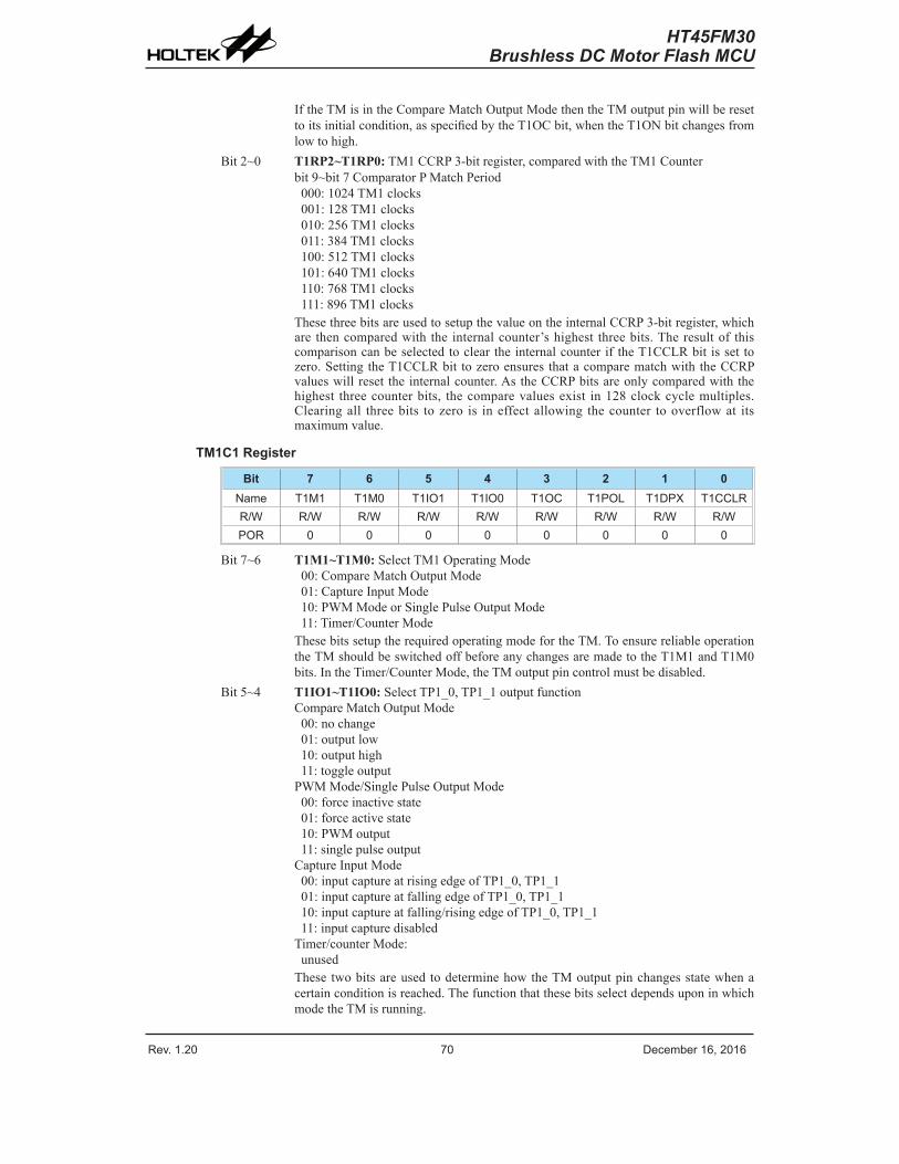
Rev. 1.20 70 De�e��e� 1�� 201� Rev. 1.20 71 De�e��e� 1�� 201�
HT45FM30Brushless DC Motor Flash MCU
IftheTMisintheCompareMatchOutputModethentheTMoutputpinwillberesettoitsinitialcondition,asspecifiedbytheT1OCbit,whentheT1ONbitchangesfromlowtohigh.
Bit2~0 T1RP2~T1RP0:TM1CCRP3-bitregister,comparedwiththeTM1Counterbit9~bit7ComparatorPMatchPeriod000:1024TM1clocks001:128TM1clocks010:256TM1clocks011:384TM1clocks100:512TM1clocks101:640TM1clocks110:768TM1clocks111:896TM1clocksThesethreebitsareusedtosetupthevalueontheinternalCCRP3-bitregister,whichare thencomparedwith the internalcounter’shighest threebits.Theresultof thiscomparisoncanbeselectedtoclear theinternalcounterif theT1CCLRbit isset tozero.SettingtheT1CCLRbit tozeroensuresthatacomparematchwiththeCCRPvalueswillreset theinternalcounter.AstheCCRPbitsareonlycomparedwiththehighest threecounterbits, thecomparevaluesexist in128clockcyclemultiples.Clearingall threebits tozero is ineffectallowing thecounter tooverflowat itsmaximumvalue.
TM1C1 Register
Bit 7 6 5 4 3 2 1 0Na�e T1M1 T1M0 T1IO1 T1IO0 T1OC T1POL T1DPX T1CCLRR/W R/W R/W R/W R/W R/W R/W R/W R/WPOR 0 0 0 0 0 0 0 0
Bit7~6 T1M1~T1M0:SelectTM1OperatingMode00:CompareMatchOutputMode01:CaptureInputMode10:PWMModeorSinglePulseOutputMode11:Timer/CounterModeThesebitssetuptherequiredoperatingmodefortheTM.ToensurereliableoperationtheTMshouldbeswitchedoffbeforeanychangesaremadetotheT1M1andT1M0bits.IntheTimer/CounterMode,theTMoutputpincontrolmustbedisabled.
Bit5~4 T1IO1~T1IO0:SelectTP1_0,TP1_1outputfunctionCompareMatchOutputMode00:nochange01:outputlow10:outputhigh11:toggleoutputPWMMode/SinglePulseOutputMode00:forceinactivestate01:forceactivestate10:PWMoutput11:singlepulseoutputCaptureInputMode00:inputcaptureatrisingedgeofTP1_0,TP1_101:inputcaptureatfallingedgeofTP1_0,TP1_110:inputcaptureatfalling/risingedgeofTP1_0,TP1_111:inputcapturedisabledTimer/counterMode:unusedThesetwobitsareusedtodeterminehowtheTMoutputpinchangesstatewhenacertainconditionisreached.ThefunctionthatthesebitsselectdependsuponinwhichmodetheTMisrunning.
Rev. 1.20 70 De�e��e� 1�� 201� Rev. 1.20 71 De�e��e� 1�� 201�
HT45FM30Brushless DC Motor Flash MCU
IntheCompareMatchOutputMode,theT1IO1andT1IO0bitsdeterminehowtheTMoutputpinchangesstatewhenacomparematchoccursfromtheComparatorA.TheTMoutputpincanbesetuptoswitchhigh,switchlowor totoggleitspresentstatewhenacomparematchoccursfromtheComparatorA.Whenthebitsarebothzero,thennochangewilltakeplaceontheoutput.TheinitialvalueoftheTMoutputpinshouldbesetupusingtheT1OCbit intheTM1C1register.NotethattheoutputlevelrequestedbytheT1IO1andT1IO0bitsmustbedifferentfromtheinitialvaluesetupusingtheT1OCbitotherwisenochangewilloccurontheTMoutputpinwhenacomparematchoccurs.AftertheTMoutputpinchangesstateitcanberesettoitsinitiallevelbychangingtheleveloftheT1ONbitfromlowtohigh.
Bit3 T1OC:TP1_0,TP1_1OutputcontrolbitCompareMatchOutputMode0:initiallow1:initialhighPWMMode/SinglePulseOutputMode0:activelow1:activehighThis is theoutputcontrolbit for theTMoutputpin. ItsoperationdependsuponwhetherTM isbeingused in theCompareMatchOutputModeor in thePWMMode/SinglePulseOutputMode.Ithasnoeffectif theTMisintheTimer/CounterMode.IntheCompareMatchOutputModeitdeterminesthelogiclevelof theTMoutputpinbeforeacomparematchoccurs. In thePWMModeitdetermines if thePWMsignalisactivehighoractivelow.
Bit2 T1POL:TP1_0,TP1_1OutputpolarityControl0:non-invert1:invertThisbitcontrolsthepolarityoftheTP1_0orTP1_1outputpin.Whenthebit issethightheTMoutputpinwillbeinvertedandnotinvertedwhenthebitiszero.IthasnoeffectiftheTMisintheTimer/CounterMode.
Bit1 T1DPX:TM1PWMperiod/dutyControl0:CCRP–period;CCRA–duty1:CCRP–duty;CCRA–periodThisbitdetermineswhichoftheCCRAandCCRPregistersareusedforperiodanddutycontrolofthePWMwaveform.
Bit0 T1CCLR:SelectTM1Counterclearcondition0:TM1ComparatorPmatch1:TM1ComparatorAmatchThisbit isused toselect themethodwhichclears thecounter.Remember that theStandardTMcontainstwocomparators,ComparatorAandComparatorP,eitherofwhichcanbeselectedtoclear the internalcounter.With theT1CCLRbitsethigh,thecounterwillbeclearedwhenacomparematchoccursfromtheComparatorA.Whenthebitislow,thecounterwillbeclearedwhenacomparematchoccursfromtheComparatorPorwithacounteroverflow.AcounteroverflowclearingmethodcanonlybeimplementediftheCCRPbitsareallclearedtozero.TheT1CCLRbitisnotusedinthePWM,SinglePulseorInputCaptureMode.
TM1DL Register
Bit 7 6 5 4 3 2 1 0Na�e D7 D� D5 D4 D3 D2 D1 D0R/W R R R R R R R RPOR 0 0 0 0 0 0 0 0
Bit7~0 TM1DL:TM1CounterLowByteRegisterbit7~bit0TM110-bitCounterbit7~bit0
Rev. 1.20 72 De�e��e� 1�� 201� Rev. 1.20 73 De�e��e� 1�� 201�
HT45FM30Brushless DC Motor Flash MCU
TM1DH Register
Bit 7 6 5 4 3 2 1 0Na�e — — — — — — D9 D8R/W — — — — — — R RPOR — — — — — — 0 0
Bit7~2 Unimplemented,readas"0"Bit1~0 TM1DH:TM1CounterHighByteRegisterbit1~bit0
TM110-bitCounterbit9~bit8
TM1AL Register
Bit 7 6 5 4 3 2 1 0Na�e D7 D� D5 D4 D3 D2 D1 D0R/W R/W R/W R/W R/W R/W R/W R/W R/WPOR 0 0 0 0 0 0 0 0
Bit7~0 TM1AL:TM1CCRALowByteRegisterbit7~bit0TM110-bitCCRAbit7~bit0
TM1AH Register
Bit 7 6 5 4 3 2 1 0Na�e — — — — — — D9 D8R/W — — — — — — R/W R/WPOR — — — — — — 0 0
Bit7~2 Unimplemented,readas"0"Bit1~0 TM1AH:TM1CCRAHighByteRegisterbit1~bit0
TM110-bitCCRAbit9~bit8
Standard Type TM Operating ModesTheStandardTypeTMcanoperateinoneoffiveoperatingmodes,CompareMatchOutputMode,PWMOutputMode,SinglePulseOutputMode,CaptureInputModeorTimer/CounterMode.TheoperatingmodeisselectedusingtheT1M1andT1M0bitsintheTM1C1register.
Compare Output ModeToselectthismode,bitsT1M1andT1M0intheTM1C1register,shouldbesetto00respectively.Inthismodeoncethecounterisenabledandrunningitcanbeclearedbythreemethods.Theseareacounteroverflow,acomparematchfromComparatorAandacomparematchfromComparatorP.WhentheT1CCLRbitislow,therearetwowaysinwhichthecountercanbecleared.OneiswhenacomparematchfromComparatorP, theotheriswhentheCCRPbitsareallzerowhichallowsthecounter tooverflow.HerebothT1AFandT1PFinterruptrequestflagsforComparatorAandComparatorPrespectively,willbothbegenerated.
IftheT1CCLRbitintheTM1C1registerishighthenthecounterwillbeclearedwhenacomparematchoccurs fromComparatorA.However,hereonly theT1AFinterrupt request flagwillbegeneratedevenifthevalueoftheCCRPbitsislessthanthatoftheCCRAregisters.ThereforewhenT1CCLRishighnoT1PFinterruptrequestflagwillbegenerated.IntheCompareMatchOutputMode,theCCRAcannotbesetto“0”.
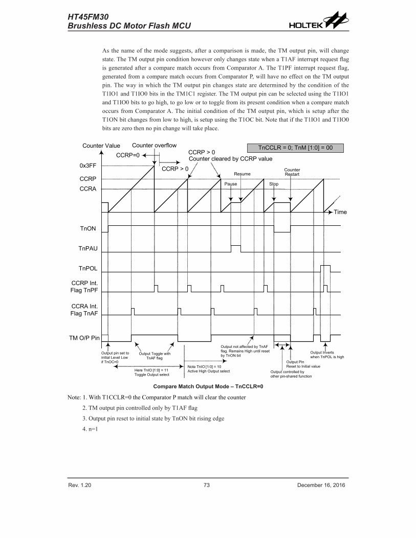
Rev. 1.20 72 De�e��e� 1�� 201� Rev. 1.20 73 De�e��e� 1�� 201�
HT45FM30Brushless DC Motor Flash MCU
Asthenameof themodesuggests,afteracomparisonismade, theTMoutputpin,willchangestate.TheTMoutputpinconditionhoweveronlychangesstatewhenaT1AFinterruptrequestflagisgeneratedafteracomparematchoccursfromComparatorA.TheT1PFinterruptrequestflag,generatedfromacomparematchoccursfromComparatorP,willhavenoeffectontheTMoutputpin.Thewayinwhich theTMoutputpinchangesstatearedeterminedby theconditionof theT1IO1andT1IO0bitsintheTM1C1register.TheTMoutputpincanbeselectedusingtheT1IO1andT1IO0bitstogohigh,togolowortotogglefromitspresentconditionwhenacomparematchoccursfromComparatorA.Theinitialconditionof theTMoutputpin,which issetupafter theT1ONbitchangesfromlowtohigh,issetupusingtheT1OCbit.NotethatiftheT1IO1andT1IO0bitsarezerothennopinchangewilltakeplace.
Counte� Value
0x3FF
CCRP
CCRA
TnON
TnPAU
TnPOL
CCRP Int. Flag TnPF
CCRA Int. Flag TnAF
TM O/P Pin
Ti�e
CCRP=0
CCRP > 0
Counte� ove�flowCCRP > 0Counte� �lea�ed �y CCRP value
Pause
Resu�e
Stop
Counte� Resta�t
TnCCLR = 0; TnM [1:0] = 00
Output pin set to initial Level Low if TnOC=0
Output Toggle with TnAF flag
Note TnIO [1:0] = 10 A�tive High Output sele�tHe�e TnIO [1:0] = 11
Toggle Output sele�t
Output not affe�ted �y TnAF flag. Re�ains High until �eset �y TnON �it
Output PinReset to Initial value
Output �ont�olled �y othe� pin-sha�ed fun�tion
Output Inve�tswhen TnPOL is high
Compare Match Output Mode – TnCCLR=0
Note:1.WithT1CCLR=0theComparatorPmatchwillclearthecounter
2.TMoutputpincontrolledonlybyT1AFflag
3.OutputpinresettoinitialstatebyTnONbitrisingedge
4.n=1
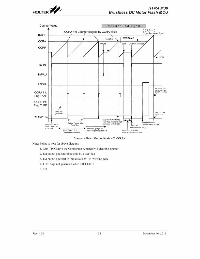
Rev. 1.20 74 De�e��e� 1�� 201� Rev. 1.20 75 De�e��e� 1�� 201�
HT45FM30Brushless DC Motor Flash MCU
Counte� Value
0x3FF
CCRP
CCRA
TnON
TnPAU
TnPOL
CCRP Int. Flag TnPF
CCRA Int. Flag TnAF
TM O/P Pin
Ti�e
CCRA=0
CCRA = 0Counte� ove�flowCCRA > 0 Counte� �lea�ed �y CCRA value
Pause
Resu�e
Stop Counte� Resta�t
TnCCLR = 1; TnM [1:0] = 00
Output pin set to initial Level Low if TnOC=0
Output Toggle with TnAF flag
Note TnIO [1:0] = 10 A�tive High Output sele�tHe�e TnIO [1:0] = 11
Toggle Output sele�t
Output not affe�ted �y TnAF flag. Re�ains High until �eset �y TnON �it
Output PinReset to Initial value
Output �ont�olled �y othe� pin-sha�ed fun�tion
Output Inve�tswhen TnPOL is high
TnPF not gene�ated
No TnAF flag gene�ated on CCRA ove�flow
Output does not �hange
Compare Match Output Mode – TnCCLR=1
Note:Pointstonoteforabovediagram:
1.WithT1CCLR=1theComparatorAmatchwillclearthecounter
2.TMoutputpincontrolledonlybyT1AFflag
3.TMoutputpinresettoinitialstatebyT1ONrisingedge
4.T1PFflagsnotgeneratedwhenT1CCLR=1
5.n=1
Rev. 1.20 74 De�e��e� 1�� 201� Rev. 1.20 75 De�e��e� 1�� 201�
HT45FM30Brushless DC Motor Flash MCU
Timer/Counter ModeToselectthismode,bitsT1M1andT1M0intheTM1C1registershouldbesetto11respectively.TheTimer/CounterModeoperates in an identicalway to theCompareMatchOutputModegeneratingthesameinterruptflags.TheexceptionisthatintheTimer/CounterModetheTMoutputpin isnotused.Therefore theabovedescriptionandTimingDiagramsfor theCompareMatchOutputModecanbeusedtounderstanditsfunction.AstheTMoutputpinisnotusedinthismode,thepincanbeusedasanormalI/Opinorotherpin-sharedfunction.
PWM Output ModeToselectthismode,bitsT1M1andT1M0intheTM1C1registershouldbesetto10respectivelyandalso theT1IO1andT1IO0bitsshouldbeset to10respectively.ThePWMfunctionwithintheTMisusefulforapplicationswhichrequirefunctionssuchasmotorcontrol,heatingcontrol,illuminationcontroletc.ByprovidingasignaloffixedfrequencybutofvaryingdutycycleontheTMoutputpin,asquarewaveACwaveformcanbegeneratedwithvaryingequivalentDCRMSvalues.AsboththeperiodanddutycycleofthePWMwaveformcanbecontrolled,thechoiceofgeneratedwaveformisextremelyflexible.InthePWMmode,theT1CCLRbithasnoeffectasthePWMperiod.BothoftheCCRAandCCRPregistersareusedtogeneratethePWMwaveform,oneregisterisusedtocleartheinternalcounterandthuscontrolthePWMwaveformfrequency,whiletheotheroneisusedtocontrolthedutycycle.WhichregisterisusedtocontroleitherfrequencyordutycycleisdeterminedusingtheT1DPXbitintheTM1C1register.
ThePWMwaveformfrequencyanddutycyclecan thereforebecontrolledby thevalues in theCCRAandCCRPregisters.An interrupt flag,one foreachof theCCRAandCCRP,willbegeneratedwhenacomparematchoccursfromeitherComparatorAorComparatorP.TheT1OCbitintheTM1C1registerisusedtoselecttherequiredpolarityofthePWMwaveformwhilethetwoT1IO1andT1IO0bitsareusedtoenablethePWMoutputortoforcetheTMoutputpintoafixedhighorlowlevel.TheT1POLbitisusedtoreversethepolarityofthePWMoutputwaveform.

Rev. 1.20 7� De�e��e� 1�� 201� Rev. 1.20 77 De�e��e� 1�� 201�
HT45FM30Brushless DC Motor Flash MCU
Counte� Value
CCRP
CCRA
TnON
TnPAU
TnPOL
CCRP Int. Flag TnPF
CCRA Int. Flag TnAF
TM O/P Pin(TnOC=1)
Ti�e
Counte� �lea�ed �y CCRP
Pause Resu�e Counte� Stop if TnON �it low
Counte� Reset when TnON �etu�ns high
TnDPX = 0; TnM [1:0] = 10
PWM Duty Cy�le set �y CCRA
PWM �esu�es ope�ation
Output �ont�olled �y othe� pin-sha�ed fun�tion Output Inve�ts
when TnPOL = 1PWM Pe�iod set �y CCRP
TM O/P Pin(TnOC=0)
PWM Mode – TnDPX=0
Note:1.HereT1DPX=0–CounterclearedbyCCRP
2.CounterClearsetsPWMPeriod
3.InternalPWMfunctioncontinuesevenwhenT1IO1,T1IO0=00or01
4.T1CCLRbithasnoinfluenceonPWMoperation
5.n=1
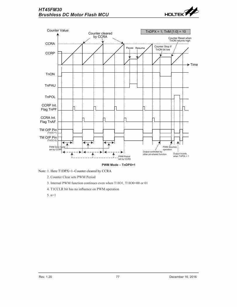
Rev. 1.20 7� De�e��e� 1�� 201� Rev. 1.20 77 De�e��e� 1�� 201�
HT45FM30Brushless DC Motor Flash MCU
Counte� Value
CCRP
CCRA
TnON
TnPAU
TnPOL
CCRP Int. Flag TnPF
CCRA Int. Flag TnAF
TM O/P Pin(TnOC=1)
Ti�e
Counte� �lea�ed �y CCRA
Pause Resu�e Counte� Stop if TnON �it low
Counte� Reset when TnON �etu�ns high
TnDPX = 1; TnM [1:0] = 10
PWM Duty Cy�le set �y CCRP
PWM �esu�es ope�ation
Output �ont�olled �y othe� pin-sha�ed fun�tion Output Inve�ts
when TnPOL = 1PWM Pe�iod set �y CCRA
TM O/P Pin(TnOC=0)
PWM Mode – TnDPX=1
Note:1.HereT1DPX=1–CounterclearedbyCCRA
2.CounterClearsetsPWMPeriod
3.InternalPWMfunctioncontinuesevenwhenT1IO1,T1IO0=00or01
4.T1CCLRbithasnoinfluenceonPWMoperation
5.n=1
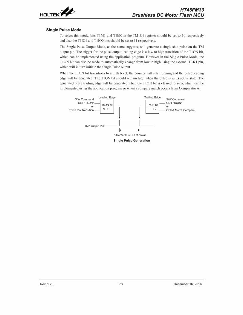
Rev. 1.20 78 De�e��e� 1�� 201� Rev. 1.20 79 De�e��e� 1�� 201�
HT45FM30Brushless DC Motor Flash MCU
Single Pulse ModeToselectthismode,bitsT1M1andT1M0intheTM1C1registershouldbesetto10respectivelyandalsotheT1IO1andT1IO0bitsshouldbesetto11respectively.
TheSinglePulseOutputMode,asthenamesuggests,willgenerateasingleshotpulseontheTMoutputpin.ThetriggerforthepulseoutputleadingedgeisalowtohightransitionoftheT1ONbit,whichcanbeimplementedusingtheapplicationprogram.HoweverintheSinglePulseMode,theT1ONbitcanalsobemadetoautomaticallychangefromlowtohighusingtheexternalTCK1pin,whichwillinturninitiatetheSinglePulseoutput.
WhentheT1ONbittransitionstoahighlevel,thecounterwillstartrunningandthepulseleadingedgewillbegenerated.TheT1ONbitshouldremainhighwhenthepulseisinitsactivestate.ThegeneratedpulsetrailingedgewillbegeneratedwhentheT1ONbitisclearedtozero,whichcanbeimplementedusingtheapplicationprogramorwhenacomparematchoccursfromComparatorA.
� � � � � � � � � � � �
� � � � � � � �� � � � �
� � � � � � � �� � � � � � � �
� �� � � � � � � � � � � � � � � � � � �
� � � � � � � �� � � � �
� � � � � � � �� � � � � � � � � �� � � � � � � � � � � � � � � � �
� � � � � � � � � � � � � � � � � � � � � � �
� � � � � � � � � � � � �
� � � � � � � � � � � � � �
Single Pulse Generation
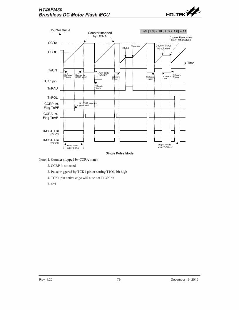
Rev. 1.20 78 De�e��e� 1�� 201� Rev. 1.20 79 De�e��e� 1�� 201�
HT45FM30Brushless DC Motor Flash MCU
Counter Value
CCRP
CCRA
TnON
TnPAU
TnPOL
CCRP Int. Flag TnPF
CCRA Int. Flag TnAF
TM O/P Pin(TnOC=1)
Time
Counter stopped by CCRA
PauseResume Counter Stops
by software
Counter Reset when TnON returns high
TnM [1:0] = 10 ; TnIO [1:0] = 11
Pulse Width set by CCRA
Output Invertswhen TnPOL = 1
No CCRP Interrupts generated
TM O/P Pin(TnOC=0)
TCKn pin
Software Trigger
Cleared by CCRA match
TCKn pin Trigger
Auto. set by TCKn pin
Software Trigger
Software Clear
Software TriggerSoftware
Trigger
Single Pulse Mode
Note:1.CounterstoppedbyCCRAmatch
2.CCRPisnotused
3.PulsetriggeredbyTCK1pinorsettingT1ONbithigh
4.TCK1pinactiveedgewillautosetT1ONbit
5.n=1
Rev. 1.20 80 De�e��e� 1�� 201� Rev. 1.20 81 De�e��e� 1�� 201�
HT45FM30Brushless DC Motor Flash MCU
HoweveracomparematchfromComparatorAwillalsoautomaticallycleartheT1ONbitandthusgeneratetheSinglePulseoutputtrailingedge.InthiswaytheCCRAvaluecanbeusedtocontrolthepulsewidth.AcomparematchfromComparatorAwillalsogenerateaTMinterrupt.Thecountercanonlyberesetback tozerowhentheT1ONbitchangesfromlowtohighwhenthecounterrestarts.IntheSinglePulseModeCCRPisnotused.TheTnCCLRandTnDPXbitsarenotusedinthisMode.
Capture Input ModeToselectthismodebitsT1M1andT1M0intheTM1C1registershouldbesetto01respectively.Thismodeenablesexternalsignals tocaptureandstore thepresentvalueof theinternalcounterandcanthereforebeusedforapplicationssuchaspulsewidthmeasurements.TheexternalsignalissuppliedontheTP1_0orTP1_1pin,whoseactiveedgecanbeeitherarisingedge,afallingedgeorbothrisingandfallingedges;theactiveedgetransitiontypeisselectedusingtheT1IO1andT1IO0bits in theTM1C1register.Thecounter isstartedwhentheT1ONbitchangesfromlowtohighwhichisinitiatedusingtheapplicationprogram.
When therequirededge transitionappearson theTP1_0orTP1_1pin thepresentvalue in thecounterwillbelatchedintotheCCRAregistersandaTMinterruptgenerated.IrrespectiveofwhateventsoccurontheTP1_0orTP1_1pinthecounterwillcontinuetofreerununtil theT1ONbitchangesfromhightolow.WhenaCCRPcomparematchoccursthecounterwillresetbacktozero;in thiswaytheCCRPvaluecanbeusedtocontrol themaximumcountervalue.WhenaCCRPcomparematchoccursfromComparatorP,aTMinterruptwillalsobegenerated.CountingthenumberofoverflowinterruptsignalsfromtheCCRPcanbeausefulmethodinmeasuringlongpulsewidths.TheT1IO1andT1IO0bitscanselecttheactivetriggeredgeontheTP1_0orTP1_1pintobearisingedge,fallingedgeorbothedgetypes.If theT1IO1andT1IO0bitsarebothsethigh,thennocaptureoperationwilltakeplaceirrespectiveofwhathappensontheTP1_0orTP1_1pin,howeveritmustbenotedthatthecounterwillcontinuetorun.
AstheTP1_0orTP1_1pinispinsharedwithotherfunctions,caremustbetakeniftheTMisintheInputCaptureMode.Thisisbecauseifthepinissetupasanoutput,thenanytransitionsonthispinmaycauseaninputcaptureoperationtobeexecuted.TheT1CCLRandT1DPXbitsarenotusedinthisMode.
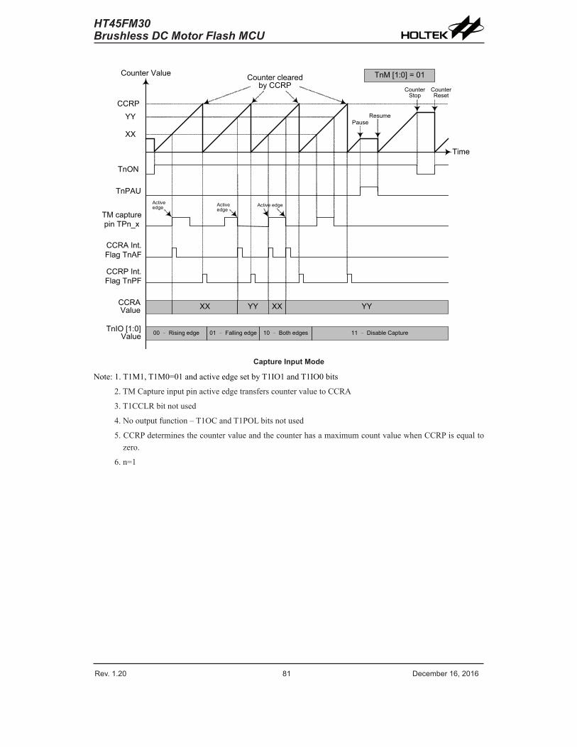
Rev. 1.20 80 De�e��e� 1�� 201� Rev. 1.20 81 De�e��e� 1�� 201�
HT45FM30Brushless DC Motor Flash MCU
Counter Value
YY
CCRP
TnON
TnPAU
CCRP Int. Flag TnPF
CCRA Int. Flag TnAF
CCRA Value
Time
Counter cleared by CCRP
PauseResume
Counter Reset
TnM [1:0] = 01
TM capture pin TPn_x
XX
Counter Stop
TnIO [1:0] Value
XX YY XX YY
Active edge Active
edgeActive edge
00 – Rising edge 01 – Falling edge 10 – Both edges 11 – Disable Capture
Capture Input Mode
Note:1.T1M1,T1M0=01andactiveedgesetbyT1IO1andT1IO0bits
2.TMCaptureinputpinactiveedgetransferscountervaluetoCCRA
3.T1CCLRbitnotused
4.Nooutputfunction–T1OCandT1POLbitsnotused
5.CCRPdeterminesthecountervalueandthecounterhasamaximumcountvaluewhenCCRPisequaltozero.
6.n=1
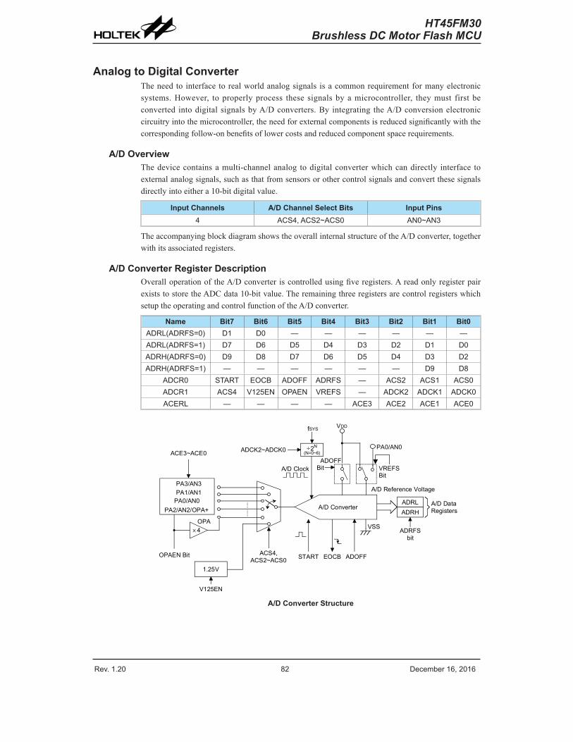
Rev. 1.20 82 De�e��e� 1�� 201� Rev. 1.20 83 De�e��e� 1�� 201�
HT45FM30Brushless DC Motor Flash MCU
Analog to Digital ConverterTheneedtointerfacetorealworldanalogsignals isacommonrequirementformanyelectronicsystems.However, toproperlyprocess these signalsbyamicrocontroller, theymust firstbeconverted intodigitalsignalsbyA/Dconverters.By integrating theA/Dconversionelectroniccircuitryintothemicrocontroller,theneedforexternalcomponentsisreducedsignificantlywiththecorrespondingfollow-onbenefitsoflowercostsandreducedcomponentspacerequirements.
A/D OverviewThedevicecontainsamulti-channelanalog todigitalconverterwhichcandirectly interface toexternalanalogsignals,suchasthatfromsensorsorothercontrolsignalsandconvertthesesignalsdirectlyintoeithera10-bitdigitalvalue.
Input Channels A/D Channel Select Bits Input Pins4 ACS4� ACS2~ACS0 AN0~AN3
TheaccompanyingblockdiagramshowstheoverallinternalstructureoftheA/Dconverter,togetherwithitsassociatedregisters.
A/D Converter Register DescriptionOveralloperationoftheA/Dconverter iscontrolledusingfiveregisters.AreadonlyregisterpairexiststostoretheADCdata10-bitvalue.TheremainingthreeregistersarecontrolregisterswhichsetuptheoperatingandcontrolfunctionoftheA/Dconverter.
Name Bit7 Bit6 Bit5 Bit4 Bit3 Bit2 Bit1 Bit0ADRL(ADRFS=0) D1 D0 — — — — — —ADRL(ADRFS=1) D7 D� D5 D4 D3 D2 D1 D0ADRH(ADRFS=0) D9 D8 D7 D� D5 D4 D3 D2ADRH(ADRFS=1) — — — — — — D9 D8
ADCR0 START EOCB ADOFF ADRFS — ACS2 ACS1 ACS0ADCR1 ACS4 V125EN OPAEN VREFS — ADCK2 ADCK1 ADCK0ACERL — — — — ACE3 ACE2 ACE1 ACE0
A/D Converter
PA3/AN3A/D Reference Voltage
ADRLADRH
A/D DataRegisters
V125EN
START EOCB ADOFF
VSS
PA0/AN0ADCK2~ADCK0
fSYS
ACE3~ACE0
ACS4,ACS2~ACS0
1.25V
A/D Clock
VDD
ADOFFBit VREFS
Bit
ADRFSbit
÷ 2N(N=0~6)
PA1/AN1PA0/AN0
PA2/AN2/OPA+
× 4OPA
OPAEN Bit
A/D Converter Structure
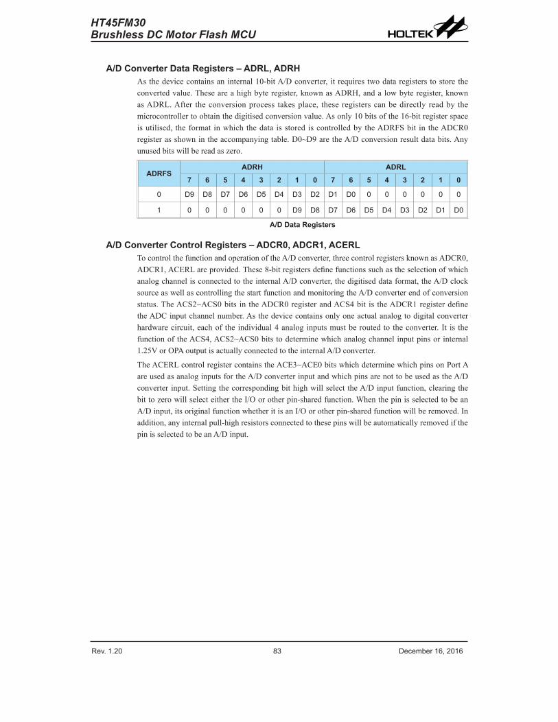
Rev. 1.20 82 De�e��e� 1�� 201� Rev. 1.20 83 De�e��e� 1�� 201�
HT45FM30Brushless DC Motor Flash MCU
A/D Converter Data Registers – ADRL, ADRHAsthedevicecontainsaninternal10-bitA/Dconverter, itrequirestwodataregisterstostoretheconvertedvalue.Theseareahighbyteregister,knownasADRH,andalowbyteregister,knownasADRL.After theconversionprocess takesplace, these registerscanbedirectly readby themicrocontrollertoobtainthedigitisedconversionvalue.Asonly10bitsofthe16-bitregisterspaceisutilised, theformat inwhichthedata isstorediscontrolledbytheADRFSbit in theADCR0registerasshownintheaccompanyingtable.D0~D9aretheA/Dconversionresultdatabits.Anyunusedbitswillbereadaszero.
ADRFSADRH ADRL
7 6 5 4 3 2 1 0 7 6 5 4 3 2 1 0
0 D9 D8 D7 D� D5 D4 D3 D2 D1 D0 0 0 0 0 0 0
1 0 0 0 0 0 0 D9 D8 D7 D� D5 D4 D3 D2 D1 D0
A/D Data Registers
A/D Converter Control Registers – ADCR0, ADCR1, ACERLTocontrolthefunctionandoperationoftheA/Dconverter,threecontrolregistersknownasADCR0,ADCR1,ACERLareprovided.These8-bitregistersdefinefunctionssuchastheselectionofwhichanalogchannelisconnectedtotheinternalA/Dconverter,thedigitiseddataformat,theA/DclocksourceaswellascontrollingthestartfunctionandmonitoringtheA/Dconverterendofconversionstatus.TheACS2~ACS0bits in theADCR0registerandACS4bit is theADCR1registerdefinetheADCinputchannelnumber.Asthedevicecontainsonlyoneactualanalogtodigitalconverterhardwarecircuit,eachof theindividual4analoginputsmustberoutedtotheconverter.It is thefunctionoftheACS4,ACS2~ACS0bitstodeterminewhichanalogchannelinputpinsorinternal1.25VorOPAoutputisactuallyconnectedtotheinternalA/Dconverter.
TheACERLcontrolregistercontainstheACE3~ACE0bitswhichdeterminewhichpinsonPortAareusedasanaloginputsfortheA/DconverterinputandwhichpinsarenottobeusedastheA/Dconverterinput.SettingthecorrespondingbithighwillselecttheA/Dinputfunction,clearingthebittozerowillselecteithertheI/Oorotherpin-sharedfunction.WhenthepinisselectedtobeanA/Dinput,itsoriginalfunctionwhetheritisanI/Oorotherpin-sharedfunctionwillberemoved.Inaddition,anyinternalpull-highresistorsconnectedtothesepinswillbeautomaticallyremovedifthepinisselectedtobeanA/Dinput.
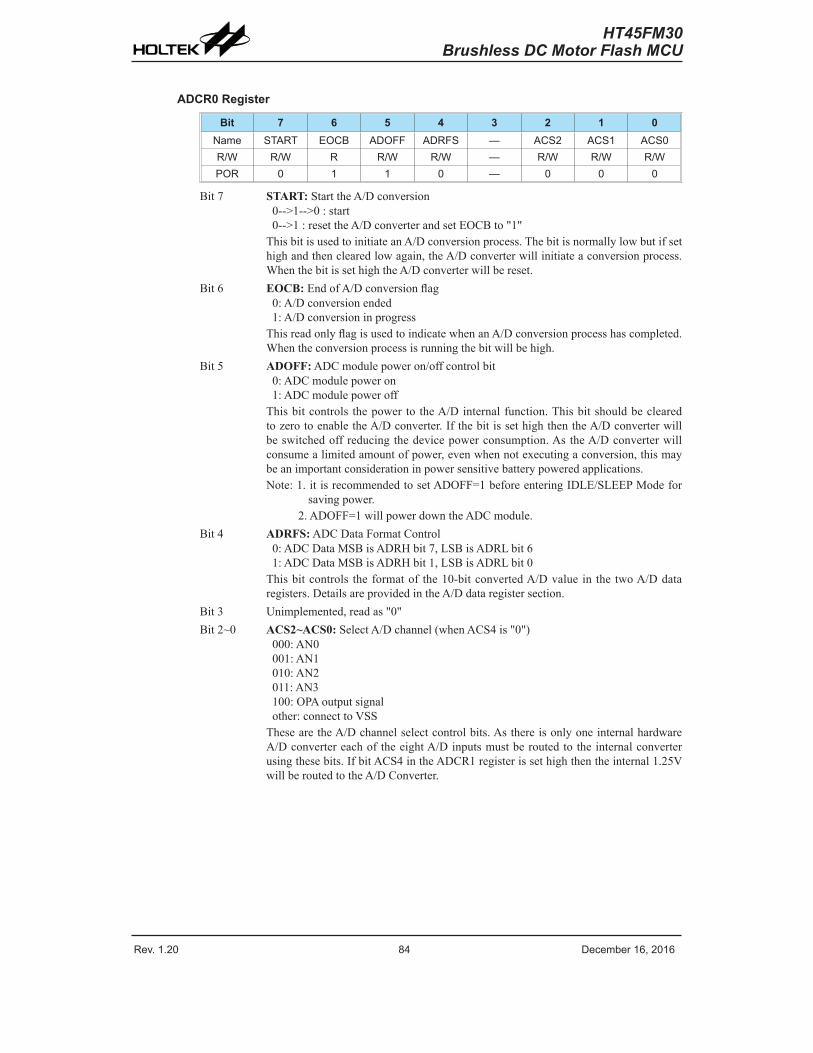
Rev. 1.20 84 De�e��e� 1�� 201� Rev. 1.20 85 De�e��e� 1�� 201�
HT45FM30Brushless DC Motor Flash MCU
ADCR0 Register
Bit 7 6 5 4 3 2 1 0Na�e START EOCB ADOFF ADRFS — ACS2 ACS1 ACS0R/W R/W R R/W R/W — R/W R/W R/WPOR 0 1 1 0 — 0 0 0
Bit7 START:StarttheA/Dconversion0-->1-->0:start0-->1:resettheA/DconverterandsetEOCBto"1"ThisbitisusedtoinitiateanA/Dconversionprocess.Thebitisnormallylowbutifsethighandthenclearedlowagain,theA/Dconverterwillinitiateaconversionprocess.WhenthebitissethightheA/Dconverterwillbereset.
Bit6 EOCB:EndofA/Dconversionflag0:A/Dconversionended1:A/DconversioninprogressThisreadonlyflagisusedtoindicatewhenanA/Dconversionprocesshascompleted.Whentheconversionprocessisrunningthebitwillbehigh.
Bit5 ADOFF:ADCmodulepoweron/offcontrolbit0:ADCmodulepoweron1:ADCmodulepoweroffThisbitcontrols thepowerto theA/Dinternalfunction.ThisbitshouldbeclearedtozerotoenabletheA/Dconverter.IfthebitissethighthentheA/Dconverterwillbeswitchedoffreducingthedevicepowerconsumption.AstheA/Dconverterwillconsumealimitedamountofpower,evenwhennotexecutingaconversion,thismaybeanimportantconsiderationinpowersensitivebatterypoweredapplications.Note:1.itisrecommendedtosetADOFF=1beforeenteringIDLE/SLEEPModeforsavingpower.
2.ADOFF=1willpowerdowntheADCmodule.Bit4 ADRFS:ADCDataFormatControl
0:ADCDataMSBisADRHbit7,LSBisADRLbit61:ADCDataMSBisADRHbit1,LSBisADRLbit0Thisbitcontrols theformatof the10-bitconvertedA/Dvaluein thetwoA/Ddataregisters.DetailsareprovidedintheA/Ddataregistersection.
Bit3 Unimplemented,readas"0"Bit2~0 ACS2~ACS0:SelectA/Dchannel(whenACS4is"0")
000:AN0001:AN1010:AN2011:AN3100:OPAoutputsignalother:connecttoVSSThesearetheA/Dchannelselectcontrolbits.AsthereisonlyoneinternalhardwareA/DconvertereachoftheeightA/Dinputsmustberoutedtotheinternalconverterusingthesebits.IfbitACS4intheADCR1registerissethighthentheinternal1.25VwillberoutedtotheA/DConverter.
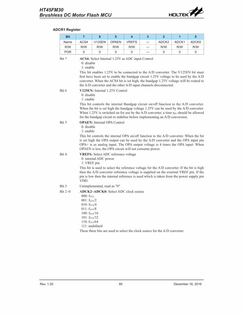
Rev. 1.20 84 De�e��e� 1�� 201� Rev. 1.20 85 De�e��e� 1�� 201�
HT45FM30Brushless DC Motor Flash MCU
ADCR1 Register
Bit 7 6 5 4 3 2 1 0Na�e ACS4 V125EN OPAEN VREFS — ADCK2 ADCK1 ADCK0R/W R/W R/W R/W R/W — R/W R/W R/WPOR 0 0 0 0 — 0 0 0
Bit7 ACS4:SelectInternal1.25VasADCinputControl0:disable1:enableThisbitenables1.25VtobeconnectedtotheA/Dconverter.TheV125ENbitmustfirsthavebeensettoenablethebandgapcircuit1.25VvoltagetobeusedbytheA/Dconverter.WhentheACS4bitissethigh,thebandgap1.25VvoltagewillberoutedtotheA/DconverterandtheotherA/Dinputchannelsdisconnected.
Bit6 V125EN:Internal1.25VControl0:disable1:enableThisbitcontrols the internalBandgapcircuiton/offfunctionto theA/Dconverter.Whenthebitissethighthebandgapvoltage1.25VcanbeusedbytheA/Dconverter.When1.25VisswitchedonforusebytheA/Dconverter,atimetBGshouldbeallowedforthebandgapcircuittostabilisebeforeimplementinganA/Dconversion.
Bit5 OPAEN: InternalOPAControl0:disable1:enableThisbitcontrolstheinternalOPAon/offfunctiontotheA/Dconverter.WhenthebitissethightheOPAoutputcanbeusedbytheA/DconverterandtheOPAinputpinOPA+isasanaloginput.TheOPAoutputvoltageis4 timestheOPAinput.WhenOPAENislow,theOPAcircuitwillnotconsumepower.
Bit4 VREFS:SelectADCreferencevoltage0:internalADCpower1:VREFpinThisbitisusedtoselectthereferencevoltagefortheA/Dconverter.IfthebitishighthentheA/DconverterreferencevoltageissuppliedontheexternalVREFpin.IfthepinislowthentheinternalreferenceisusedwhichistakenfromthepowersupplypinVDD.
Bit3 Unimplemented,readas"0"Bit2~0 ADCK2~ADCK0:SelectADCclocksource
000:fSYS001:fSYS/2010:fSYS/4011:fSYS/8100:fSYS/16101:fSYS/32110:fSYS/64111:undefinedThesethreebitsareusedtoselecttheclocksourcefortheA/Dconverter.
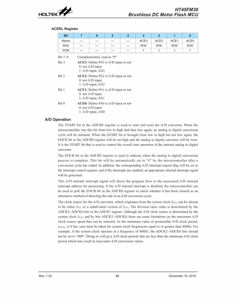
Rev. 1.20 8� De�e��e� 1�� 201� Rev. 1.20 87 De�e��e� 1�� 201�
HT45FM30Brushless DC Motor Flash MCU
ACERL Register
Bit 7 6 5 4 3 2 1 0Na�e — — — — ACE3 ACE2 ACE1 ACE0R/W — — — — R/W R/W R/W R/WPOR — — — — 1 1 1 1
Bit7~4 Unimplemented,readas"0"Bit3 ACE3:DefinePA3isA/Dinputornot
0:notA/Dinput1:A/Dinput,AN3
Bit2 ACE2:DefinePA2isA/Dinputornot0:notA/Dinput1:A/Dinput,AN2
Bit1 ACE1:DefinePA1isA/Dinputornot0:notA/Dinput1:A/Dinput,AN1
Bit0 ACE0:DefinePA0isA/Dinputornot0:notA/Dinput1:A/Dinput,AN0
A/D OperationTheSTARTbit in theADCR0register isused tostartand reset theA/Dconverter.When themicrocontrollersetsthisbitfromlowtohighandthenlowagain,ananalogtodigitalconversioncyclewillbe initiated.WhentheSTARTbit isbroughtfromlowtohighbutnot lowagain, theEOCBbitintheADCR0registerwillbesethighandtheanalogtodigitalconverterwillbereset.ItistheSTARTbitthatisusedtocontroltheoverallstartoperationoftheinternalanalogtodigitalconverter.
TheEOCBbit in theADCR0register isused to indicatewhentheanalogtodigitalconversionprocess is complete.Thisbitwillbeautomatically set to “0”by themicrocontroller after aconversioncyclehasended.Inaddition,thecorrespondingA/Dinterruptrequestflagwillbesetintheinterruptcontrolregister,andiftheinterruptsareenabled,anappropriateinternalinterruptsignalwillbegenerated.
ThisA/D internal interrupt signalwilldirect theprogramflow to theassociatedA/D internalinterruptaddressforprocessing.If theA/Dinternal interrupt isdisabled, themicrocontrollercanbeusedtopoll theEOCBbit in theADCR0register tocheckwhether ithasbeenclearedasanalternativemethodofdetectingtheendofanA/Dconversioncycle.
TheclocksourcefortheA/Dconverter,whichoriginatesfromthesystemclockfSYS,canbechosentobeeither fSYSorasubdividedversionof fSYS.Thedivisionratiovalue isdeterminedby theADCK2~ADCK0bitsintheADCR1register.AlthoughtheA/DclocksourceisdeterminedbythesystemclockfSYS,andbybitsADCK2~ADCK0,therearesomelimitationsonthemaximumA/Dclocksourcespeedthatcanbeselected.AstheminimumvalueofpermissibleA/Dclockperiod,tADCK,is0.5µs,caremustbetakenforsystemclockfrequenciesequaltoorgreaterthan4MHz.Forexample, if thesystemclockoperatesatafrequencyof4MHz,theADCK2~ADCK0bitsshouldnotbesetto“000”.DoingsowillgiveA/DclockperiodsthatarelessthantheminimumA/DclockperiodwhichmayresultininaccurateA/Dconversionvalues.
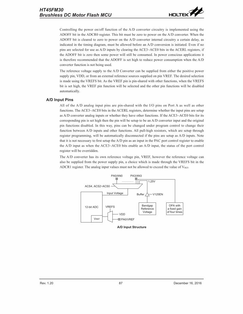
Rev. 1.20 8� De�e��e� 1�� 201� Rev. 1.20 87 De�e��e� 1�� 201�
HT45FM30Brushless DC Motor Flash MCU
Controlling thepoweron/off functionof theA/Dconvertercircuitry is implementedusing theADOFFbitintheADCR0register.ThisbitmustbezerotopowerontheA/Dconverter.WhentheADOFFbit isclearedtozerotopowerontheA/Dconverter internalcircuitryacertaindelay,asindicatedinthetimingdiagram,mustbeallowedbeforeanA/Dconversionisinitiated.EvenifnopinsareselectedforuseasA/DinputsbyclearingtheACE3~ACE0bitsintheACERLregisters,iftheADOFFbitiszerothensomepowerwillstillbeconsumed.InpowerconsciousapplicationsitisthereforerecommendedthattheADOFFissethightoreducepowerconsumptionwhentheA/Dconverterfunctionisnotbeingused.
ThereferencevoltagesupplytotheA/DConvertercanbesuppliedfromeitherthepositivepowersupplypin,VDD,orfromanexternalreferencesourcessuppliedonpinVREF.ThedesiredselectionismadeusingtheVREFSbit.AstheVREFpinispin-sharedwithotherfunctions,whentheVREFSbitissethigh,theVREFpinfunctionwillbeselectedandtheotherpinfunctionswillbedisabledautomatically.
A/D Input PinsAllof theA/Danalog inputpinsarepin-sharedwith the I/OpinsonPortAaswellasotherfunctions.TheACE3~ACE0bitsintheACERLregisters,determinewhethertheinputpinsaresetupasA/Dconverteranaloginputsorwhethertheyhaveotherfunctions.IftheACE3~ACE0bitsforitscorrespondingpinissethighthenthepinwillbesetuptobeanA/Dconverterinputandtheoriginalpinfunctionsdisabled. In thisway,pinscanbechangedunderprogramcontrol tochange theirfunctionbetweenA/Dinputsandotherfunctions.Allpull-highresistors,whicharesetupthroughregisterprogramming,willbeautomaticallydisconnectedifthepinsaresetupasA/Dinputs.NotethatitisnotnecessarytofirstsetuptheA/DpinasaninputinthePACportcontrolregistertoenabletheA/DinputaswhentheACE3~ACE0bitsenableanA/Dinput, thestatusof theportcontrolregisterwillbeoverridden.
TheA/Dconverterhas itsownreferencevoltagepin,VREF,however thereferencevoltagecanalsobesuppliedfromthepowersupplypin,achoicewhichismadethroughtheVREFSbitintheADCR1register.TheanaloginputvaluesmustnotbeallowedtoexceedthevalueofVREF.
� � � � � � � � � � � � � �
� � � � �
� � � � � �� � � � � �
� � � � � � �
� � �
� � � �
� � �
� � � � � � � � � � � � � � �� � � � � � � � �� � � � � � �
� � � � � � � � � � � � �
� � � � � � � � � � � � �
� � � � � � � �� � � � � � � � � � � �� � � � � � � � � � � � �
A/D Input Structure
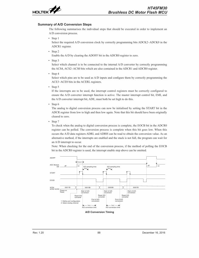
Rev. 1.20 88 De�e��e� 1�� 201� Rev. 1.20 89 De�e��e� 1�� 201�
HT45FM30Brushless DC Motor Flash MCU
Summary of A/D Conversion StepsThefollowingsummarisestheindividualstepsthatshouldbeexecutedinordertoimplementanA/Dconversionprocess.
• Step1SelecttherequiredA/DconversionclockbycorrectlyprogrammingbitsADCK2~ADCK0intheADCR1register.
• Step2EnabletheA/DbyclearingtheADOFFbitintheADCR0registertozero.
• Step3SelectwhichchannelistobeconnectedtotheinternalA/DconverterbycorrectlyprogrammingtheACS4,ACS2~ACS0bitswhicharealsocontainedintheADCR1andADCR0register.
• Step4SelectwhichpinsaretobeusedasA/DinputsandconfigurethembycorrectlyprogrammingtheACE3~ACE0bitsintheACERLregisters.
• Step5If the interruptsare tobeused, the interruptcontrolregistersmustbecorrectlyconfigured toensuretheA/Dconverterinterruptfunctionisactive.Themasterinterruptcontrolbit,EMI,andtheA/Dconverterinterruptbit,ADE,mustbothbesethightodothis.
• Step6TheanalogtodigitalconversionprocesscannowbeinitialisedbysettingtheSTARTbit intheADCRregisterfromlowtohighandthenlowagain.Notethatthisbitshouldhavebeenoriginallyclearedtozero.
• Step7Tocheckwhentheanalogtodigitalconversionprocessiscomplete,theEOCBbitintheADCR0registercanbepolled.Theconversionprocess iscompletewhenthisbitgoes low.WhenthisoccurstheA/DdataregistersADRLandADRHcanbereadtoobtaintheconversionvalue.Asanalternativemethod,iftheinterruptsareenabledandthestackisnotfull,theprogramcanwaitforanA/Dinterrupttooccur.Note:Whencheckingfortheendoftheconversionprocess,ifthemethodofpollingtheEOCBbitintheADCR0registerisused,theinterruptenablestepabovecanbeomitted.
� � � �� � � � � � � � � � � � � � � � � � �
� � � � � � � � � � � �
� � � �
� �
� � � � �� � � � � � �
� � � � � � � �� � � � �
� � � � � � � � �� � � � � � � � � �� � � � � � � � � � � � � � � � � � � � � � � � � � � �
� � � � � � � � � � � � � � � � � � �
� � � � � � � � � � �� � � � � � � � � �
� � � � � � � � �� � � � � � � � �
� � � � � � � � � � � � � � � �� � � � � �
� � � � � �
� � � � � � � � � � �� � � � � � � � � �
� � � � � � � � �� � � � � � � � �
� � � � � �
� � � � � � � � � � �� � � � � � � � � �
� � � � � � � � �� � � � � � � � �
� � � � � � � � �� � � � � � � � � �
� � � � � � � � � � � � � � � �� � � � � �
� � � � �� �
� � � �
� � � �� � � � � � � � � � � � � � � � � � �
� � �
� � � �
� � � � � � � � � �
A/D Conversion Timing
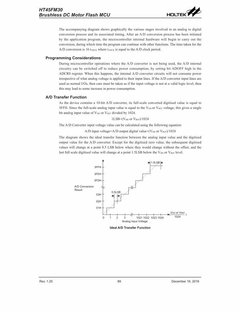
Rev. 1.20 88 De�e��e� 1�� 201� Rev. 1.20 89 De�e��e� 1�� 201�
HT45FM30Brushless DC Motor Flash MCU
Theaccompanyingdiagramshowsgraphicallythevariousstagesinvolvedinananalogtodigitalconversionprocessanditsassociatedtiming.AfteranA/Dconversionprocesshasbeeninitiatedby theapplicationprogram, themicrocontroller internalhardwarewillbegin tocarryout theconversion,duringwhichtimetheprogramcancontinuewithotherfunctions.ThetimetakenfortheA/Dconversionis16tADCKwheretADCKisequaltotheA/Dclockperiod.
Programming ConsiderationsDuringmicrocontrolleroperationswhere theA/Dconverter isnotbeingused, theA/Dinternalcircuitrycanbeswitchedoff to reducepowerconsumption,bysettingbitADOFFhigh in theADCR0register.Whenthishappens, theinternalA/Dconvertercircuitswillnotconsumepowerirrespectiveofwhatanalogvoltageisappliedtotheirinputlines.IftheA/DconverterinputlinesareusedasnormalI/Os,thencaremustbetakenasiftheinputvoltageisnotatavalidlogiclevel,thenthismayleadtosomeincreaseinpowerconsumption.
A/D Transfer FunctionAsthedevicecontainsa10-bitA/Dconverter, itsfull-scaleconverteddigitisedvalueisequal to3FFH.Sincethefull-scaleanaloginputvalueisequaltotheVDDorVREFvoltage,thisgivesasinglebitanaloginputvalueofVDDorVREFdividedby1024.
1LSB=(VDDorVREF)/1024
TheA/DConverterinputvoltagevaluecanbecalculatedusingthefollowingequation:
A/Dinputvoltage=A/Doutputdigitalvalue×(VDDorVREF)/1024
Thediagramshowsthe ideal transferfunctionbetweentheanaloginputvalueandthedigitisedoutputvaluefor theA/Dconverter.Exceptfor thedigitisedzerovalue, thesubsequentdigitisedvalueswillchangeatapoint0.5LSBbelowwheretheywouldchangewithouttheoffset,andthelastfullscaledigitisedvaluewillchangeatapoint1.5LSBbelowtheVDDorVREFlevel.
�
� � � � � � � � � � � � � �� � � � � �
� � �
� � �
� � �
� �
�
�
� � � � � �
� � � � �
� � � � � � � � � � � � � � � � � � � � � � � � � � � � � � � � � �
� � � � � � � � � � �
� �� � � � � � � � � � � � � � � � � � � � � �
� � � � � � � � � � � � � � � � � � � �
Ideal A/D Transfer Function
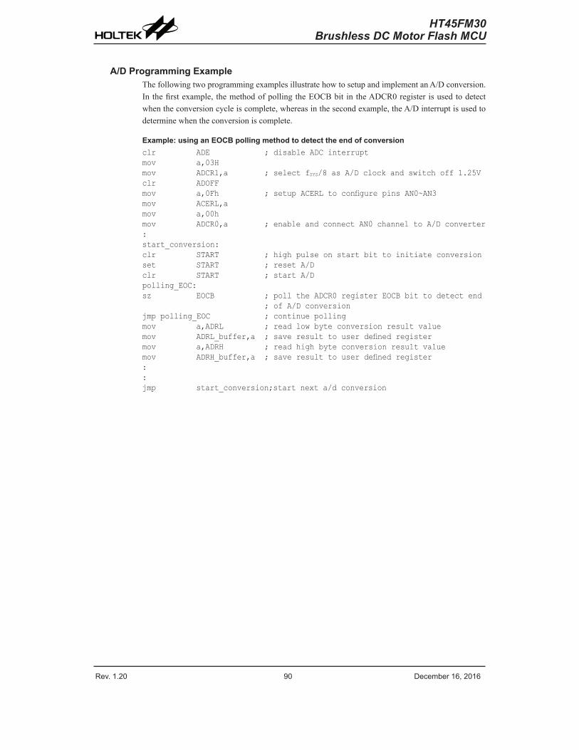
Rev. 1.20 90 De�e��e� 1�� 201� Rev. 1.20 91 De�e��e� 1�� 201�
HT45FM30Brushless DC Motor Flash MCU
A/D Programming ExampleThefollowingtwoprogrammingexamplesillustratehowtosetupandimplementanA/Dconversion.Inthefirstexample, themethodofpollingtheEOCBbit intheADCR0registerisusedtodetectwhentheconversioncycleiscomplete,whereasinthesecondexample,theA/Dinterruptisusedtodeterminewhentheconversioniscomplete.
Example: using an EOCB polling method to detect the end of conversionclr ADE ; disable ADC interruptmov a,03Hmov ADCR1,a ;selectfSYS/8asA/Dclockandswitchoff1.25Vclr ADOFFmov a,0Fh ;setupACERLtoconfigurepinsAN0~AN3mov ACERL,amov a,00hmov ADCR0,a ;enableandconnectAN0channeltoA/Dconverter:start_conversion:clr START ;highpulseonstartbittoinitiateconversionset START ;resetA/Dclr START ;startA/Dpolling_EOC:sz EOCB ;polltheADCR0registerEOCBbittodetectend ;ofA/Dconversionjmppolling_EOC ;continuepollingmov a,ADRL ;readlowbyteconversionresultvaluemov ADRL_buffer,a ;saveresulttouserdefinedregistermov a,ADRH ;readhighbyteconversionresultvaluemov ADRH_buffer,a;saveresulttouserdefinedregister::jmp start_conversion;startnexta/dconversion
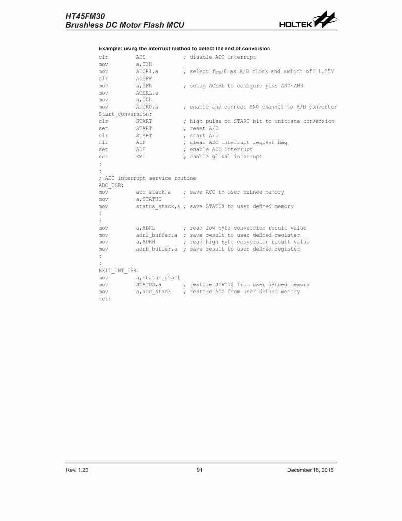
Rev. 1.20 90 De�e��e� 1�� 201� Rev. 1.20 91 De�e��e� 1�� 201�
HT45FM30Brushless DC Motor Flash MCU
Example: using the interrupt method to detect the end of conversionclr ADE ; disable ADC interruptmov a,03Hmov ADCR1,a ;selectfSYS/8asA/Dclockandswitchoff1.25Vclr ADOFFmov a,0Fh ;setupACERLtoconfigurepinsAN0~AN3mov ACERL,amov a,00hmov ADCR0,a ;enableandconnectAN0channeltoA/DconverterStart_conversion:clr START ;highpulseonSTARTbittoinitiateconversionset START ;resetA/Dclr START ;startA/Dclr ADF ;clearADCinterruptrequestflagset ADE ; enable ADC interruptset EMI ;enableglobalinterrupt::; ADC interrupt service routineADC_ISR:mov acc_stack,a ;saveACCtouserdefinedmemorymov a,STATUSmov status_stack,a;saveSTATUStouserdefinedmemory::mov a,ADRL ;readlowbyteconversionresultvaluemov adrl_buffer,a ;saveresulttouserdefinedregistermov a,ADRH ;readhighbyteconversionresultvaluemov adrh_buffer,a ;saveresulttouserdefinedregister::EXIT_INT_ISR:mov a,status_stackmov STATUS,a ;restoreSTATUSfromuserdefinedmemorymov a,acc_stack ;restoreACCfromuserdefinedmemoryreti
Rev. 1.20 92 De�e��e� 1�� 201� Rev. 1.20 93 De�e��e� 1�� 201�
HT45FM30Brushless DC Motor Flash MCU
Operational Amplifier – OPAThedeviceincludesaninternalOPAwithafixedgainoffourtimes.TheoutputcanbeconnectedtotheA/DconverterortothenegativeinputofthecomparatorCMP0.
� � � �� � �
� � � � � � � � � � � � � � � � � � � � � �� � � � � � � � � � �
� � �
Operational Amplifier RegistersTheinternalOperationalAmplifierisfullyunderthecontrolofinternalregisters,ADCR0,ADCR1,CP0CandOPAC.These registerscontrol the inputpathselection,enable/disable functionandcalibrationfunction.
Operational Amplifier OperationWhentheACS2~ACS0bitsintheADCR0registerintheA/Dconverteraresetto100B,thentheOPAoutputwillbeselectedasA/Dconverterinput.
TheOPAENbit in theADCR1 register isusedas theenable/disablebit for theOperationalAmplifier.WhenthebitissethightheOPAoutputisusedbytheA/DconverterandtheOPAinputpinOPA+isasanaloginput.TheOPAoutputvoltageis4timesoftheOPAinput.WhentheOPAENislow,theOPAisdisabledandpoweredofftoreducepowerconsumption.
TheC0NOPAbitintheCP0Cregisterisusedastheenable/disablebitforOPAoutputtoconnecttoC0-.whenthebitissethigh,theOPAoutputcanbeconnectedtoC0-.
ADCR0 Register
Bit 7 6 5 4 3 2 1 0Na�e START EOCB ADOFF ADRFS — ACS2 ACS1 ACS0R/W R/W R R/W R/W — R/W R/W R/WPOR 0 1 1 0 — 0 0 0
Bit7~3 A/DConverterrelatedregisters,describedelsewhereBit2~0 ACS2~ACS0:SelectA/Dchannel(whenACS4is"0")
000:AN0001:AN1010:AN2011:AN3100:OPAoutputsignalother:connecttoVSS
ADCR1 Register
Bit 7 6 5 4 3 2 1 0Na�e ACS4 V125EN OPAEN VREFS — ADCK2 ADCK1 ADCK0R/W R/W R/W R/W R/W — R/W R/W R/WPOR 0 0 0 0 — 0 0 0
Bit7,6,4~0 A/DConverterrelatedregisters,describedelsewhereBit5 OPAEN:InternalOPAControl
0:disable1:enableThisbitcontrolstheinternalOPAon/offfunctiontotheA/Dconverter.WhenthebitissethightheOPAoutputcanbeusedbytheA/DconverterandtheOPAinputpinOPA+isasanaloginput.TheOPAoutputvoltageis4timesoftheOPAinput.WhentheOPAENislow,theOPAcircuitwillnotconsumepower.
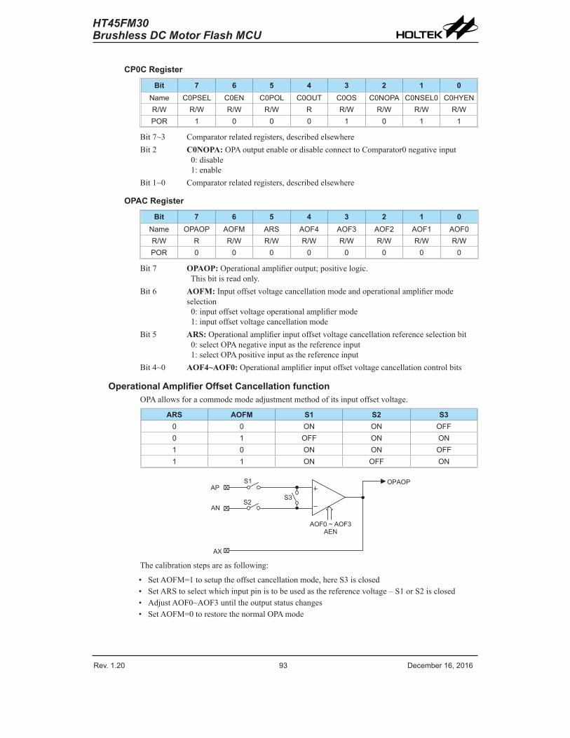
Rev. 1.20 92 De�e��e� 1�� 201� Rev. 1.20 93 De�e��e� 1�� 201�
HT45FM30Brushless DC Motor Flash MCU
CP0C Register
Bit 7 6 5 4 3 2 1 0Na�e C0PSEL C0EN C0POL C0OUT C0OS C0NOPA C0NSEL0 C0HYENR/W R/W R/W R/W R R/W R/W R/W R/WPOR 1 0 0 0 1 0 1 1
Bit7~3 Comparatorrelatedregisters,describedelsewhereBit2 C0NOPA:OPAoutputenableordisableconnecttoComparator0negativeinput
0:disable1:enable
Bit1~0 Comparatorrelatedregisters,describedelsewhere
OPAC Register
Bit 7 6 5 4 3 2 1 0Na�e OPAOP AOFM ARS AOF4 AOF3 AOF2 AOF1 AOF0R/W R R/W R/W R/W R/W R/W R/W R/WPOR 0 0 0 0 0 0 0 0
Bit7 OPAOP:Operationalamplifieroutput;positivelogic.Thisbitisreadonly.
Bit6 AOFM:Inputoffsetvoltagecancellationmodeandoperationalamplifiermodeselection0:inputoffsetvoltageoperationalamplifiermode1:inputoffsetvoltagecancellationmode
Bit5 ARS:Operationalamplifierinputoffsetvoltagecancellationreferenceselectionbit0:selectOPAnegativeinputasthereferenceinput1:selectOPApositiveinputasthereferenceinput
Bit4~0 AOF4~AOF0:Operationalamplifierinputoffsetvoltagecancellationcontrolbits
Operational Amplifier Offset Cancellation functionOPAallowsforacommodemodeadjustmentmethodofitsinputoffsetvoltage.
ARS AOFM S1 S2 S30 0 ON ON OFF0 1 OFF ON ON1 0 ON ON OFF1 1 ON OFF ON
� �
� �� �
� � � � � � � � � � �� � �
� �
� �
� �� � � � �
Thecalibrationstepsareasfollowing:
• SetAOFM=1tosetuptheoffsetcancellationmode,hereS3isclosed• SetARStoselectwhichinputpinistobeusedasthereferencevoltage–S1orS2isclosed• AdjustAOF0~AOF3untiltheoutputstatuschanges• SetAOFM=0torestorethenormalOPAmode
Rev. 1.20 94 De�e��e� 1�� 201� Rev. 1.20 95 De�e��e� 1�� 201�
HT45FM30Brushless DC Motor Flash MCU
ComparatorsFourcomparatorsarecontainedwithin thisdevice.Thesecomparatorsarecontrolledby theregisters,CP0C,CP1C,CP2CandCP3C,offering the flexible features, suchaspower-down,polarityselection,hysteresisselectionetc.ThecomparatorsI/Osarepin-sharedwiththeotherpins.Ifthecomparatorfunctionisnotselected,thedesignercanassignthecorrespondingI/Opinstotheotherfunctions.
C0+
C0-
C1-
OPA output
8-bit DAC
-
+Comparator 0
C0POL C0OUT
C0SEL
C0X
C1+
-
+Comparator 1
C1POL C1OUT
C1SEL
C1X
C1-
C2+
C2- -
+Comparator 2
C2POL C2OUT
C2SEL
C2X
C1-
C3+
C3- -
+Comparator 3
C3POL C3OUT
C3SEL
C3X
Comparator OperationThedevicecontains fourcomparatorswhichareused tocompare inputsignalsand toprovideanoutputbasedon theirdifference.Thesefour internalcomparatorsarefullycontrolledby thecontrolregisters,CP0C~CP3C.Thecomparatoroutputcanbereadbyabit,namelyCnOUT, inthecorrespondingcontrolregistersandcanbetransferredout toanI/Opinaswell. Inaddition,theoutputpolarity,hysteresisandpowerdownfunctionsareincludedinthesecomparators.Anypull-highresistorsconnectedtothesharedcomparatorinputpinswillbeautomaticallydisconnectedwhenthecomparatorisenabled.
As thecomparator inputsapproach theirswitching level,somespuriousoutputsignalsmaybegeneratedonthecomparatoroutputduetotheslowrisingorfallingnatureoftheinputsignals.Thiscanbeminimisedbyselectingthehysteresisfunctionwillapplyasmallamountofpositivefeedbacktothecomparator.Ideallythecomparatorshouldswitchatthepointwherethepositiveandnegativeinputssignalsareat thesamevoltage level;however,unavoidable inputoffsets introducesomeuncertaintieshere.Thehysteresisfunction,ifenabled,alsoincreasestheswitchingoffsetvalue.
Thecomparatorshavetheirowninterruptwhichisdescribedintheinterruptsection.
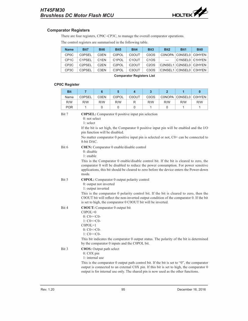
Rev. 1.20 94 De�e��e� 1�� 201� Rev. 1.20 95 De�e��e� 1�� 201�
HT45FM30Brushless DC Motor Flash MCU
Comparator RegistersTherearefourregisters,CP0C~CP3C,tomanagetheoverallcomparatoroperations.
Thecontrolregistersaresummarisedinthefollowingtable.
Name Bit7 Bit6 Bit5 Bit4 Bit3 Bit2 Bit1 Bit0CP0C C0PSEL C0EN C0POL C0OUT C0OS C0NOPA C0NSEL0 C0HYENCP1C C1PSEL C1EN C1POL C1OUT C1OS — C1NSEL0 C1HYENCP2C C2PSEL C2EN C2POL C2OUT C2OS C2NSEL1 C2NSEL0 C2HYENCP3C C3PSEL C3EN C3POL C3OUT C3OS C3NSEL1 C3NSEL0 C3HYEN
Comparator Registers List
CP0C Register
Bit 7 6 5 4 3 2 1 0Na�e C0PSEL C0EN C0POL C0OUT C0OS C0NOPA C0NSEL0 C0HYENR/W R/W R/W R/W R R/W R/W R/W R/WPOR 1 0 0 0 1 0 1 1
Bit7 C0PSEL:Comparator0positiveinputpinselection0:notselect1:selectIfthebitissethigh,theComparator0positiveinputpinwillbeenabledandtheI/Opinfunctionwillbedisabled.Nomattercomparator0positiveinputpinisselectedornot,C0+canbeconnectedto8-bitDAC.
Bit6 C0EN: Comparator0enable/disablecontrol0:disable1:enableThisis theComparator0enable/disablecontrolbit.If thebit isclearedtozero, thecomparator0willbedisabledtoreducethepowerconsumption.Forpowersensitiveapplications,thisbitshouldbeclearedtozerobeforethedeviceentersthePower-downmode.
Bit5 C0POL:Comparator0outputpolaritycontrol0:outputnotinverted1:outputinvertedThis is thecomparator0polaritycontrolbit. If thebit iscleared tozero, then theC0OUTbitwillreflectthenon-invertedoutputconditionofthecomparator0.Ifthebitissettohigh,thecomparator0C0OUTbitwillbeinverted.
Bit4 C0OUT:Comparator0outputbitC0POL=00:C0+<C0-1:C0+>C0-C0POL=10:C0+>C0-1:C0+<C0-Thisbitindicatesthecomparator0outputstatus.Thepolarityofthebitisdeterminedbythecomparator0inputsandtheC0POLbit.
Bit3 C0OS:Outputpathselect0:C0Xpin1:internaluseThisisthecomparator0outputpathcontrolbit.Ifthebitissetto“0”,thecomparatoroutputisconnectedtoanexternalC0Xpin.Ifthisbitissettohigh,thecomparator0outputisforinternaluseonly.Thesharedpinisnowusedastheotherfunctions.
Rev. 1.20 9� De�e��e� 1�� 201� Rev. 1.20 97 De�e��e� 1�� 201�
HT45FM30Brushless DC Motor Flash MCU
Bit2 C0NOPA:OPAoutputconnectstocomparator0negativeinputcontrolbit0:disable1:enable
Bit1 C0NSEL: SelectComparator0negativeinputpinornot0:notselect1:selectThis is theComparator0pinselection.If thebit is set tohigh, theComparator0negative inputpinwillbeenabled.Asa result, thepinwilldisable the I/Opinfunctions.Nomatter thecomparator0negative inputpin is selectedornot, theC0-canbeconnectedtoOPAoutput.
Bit0 C0HYEN:HysteresisControl0:disable1:enableThis is thehysteresiscontrolbitand if thisbit issethigh, itwillapplya limitedamountofhysteresis to thecomparator0,asspecifiedintheComparatorElectricalCharacteristicstable.Thepositivefeedbackinducedbyhysteresisreducestheeffectofspuriousswitchingnearthecomparatorthreshold.
CP1C Register
Bit 7 6 5 4 3 2 1 0Na�e C1PSEL C1EN C1POL C1OUT C1OS — C1NSEL0 C1HYENR/W R/W R/W R/W R R/W — R/W R/WPOR 1 0 0 0 1 — 1 1
Bit7 C1PSEL: Comparator1positiveinputpinselection0:notselect1:selectIfthebitissethigh,theComparator1positiveinputpinwillbeenabledandtheI/Opinfunctionwillbedisabled.
Bit6 C1EN:Comparator1enable/disablecontrol0:disable1:enableThisis theComparator1enable/disablecontrolbit.If thebit isclearedtozero, thecomparator1willbedisabledtoreducethepowerconsumption.Forpowersensitiveapplications,thisbitshouldbeclearedtozerobeforethedeviceentersthePower-downmode.
Bit5 C1POL:Comparator1outputpolaritycontrol0:outputnotinverted1:outputinvertedThis is thecomparator1polaritycontrolbit. If thebit iscleared tozero, then theC1OUTbitwillreflectthenon-invertedoutputconditionofthecomparator1.Ifthebitissettohigh,thecomparator1C1OUTbitwillbeinverted.
Bit4 C1OUT:Comparator1outputbitC1POL=00:C1+<C1-1:C1+>C1-C1POL=10:C1+>C1-1:C1+<C1-Thisbitindicatesthecomparator1outputstatus.Thepolarityofthebitisdeterminedbythecomparator1inputsandtheC1POLbit.
Rev. 1.20 9� De�e��e� 1�� 201� Rev. 1.20 97 De�e��e� 1�� 201�
HT45FM30Brushless DC Motor Flash MCU
Bit3 C1OS:Outputpathselect0:C1Xpin1:internaluseThisisthecomparator1outputpathcontrolbit.Ifthebitissetto“0”,thecomparatoroutputisconnectedtoanexternalC1Xpin.Ifthisbitissettohigh,thecomparator1outputisforinternaluseonly.Thesharedpinisnowusedastheotherfunctions.
Bit2 Unimplemented,readas“0”Bit1 C1NSEL:SelectComparator1negativeinputpinornot
0:notselect1:selectThis is theComparator1pinselection. If thebit isset tohigh, theComparator1negative inputpinwillbeenabled.Asa result, thepinwilldisable the I/Opinfunctions.Nomatterwhetherthecomparator1negativeinputpinisselectedornot,C1-canbeconnectedto8-bitDAC.
Bit0 C1HYEN:HysteresisControl0:disable1:enableThisisthehysteresiscontrolbit.Settingthisbithighwillapplyalimitedamountofhysteresistothecomparator1,asspecifiedintheComparatorElectricalCharacteristicstable.Thepositive feedback inducedbyhysteresis reduces theeffectofspuriousswitchingnearthecomparator1threshold.
CP2C Register
Bit 7 6 5 4 3 2 1 0Na�e C2PSEL C2EN C2POL C2OUT C2OS C2NSEL1 C2NSEL0 C2HYENR/W R/W R/W R/W R R/W R/W R/W R/WPOR 1 0 0 0 1 0 1 1
Bit7 C2PSEL:Comparator2positiveinputpinselection0:notselect1:selectIfthebitissethigh,theComparator2positiveinputpinwillbeenabledandtheI/Opinfunctionwillbedisabled.
Bit6 C2EN: Comparator2enable/disablecontrol0:disable1:enableThisis theComparator2enable/disablecontrolbit.If thebit isclearedtozero, thecomparator2willbedisabledtoreducethepowerconsumption.Forpowersensitiveapplications,thisbitshouldbeclearedtozerobeforethedeviceentersthePower-downmode.
Bit5 C2POL:Comparator2outputpolaritycontrol0:outputnotinverted1:outputinvertedThis is thecomparator2polaritycontrolbit. If thebit iscleared tozero, then theC2OUTbitwillreflectthenon-invertedoutputconditionofthecomparator2.Ifthebitissettohigh,thecomparator2C2OUTbitwillbeinverted.
Bit4 C2OUT:Comparator2outputbitC2POL=00:C2+<C2-1:C2+>C2-C2POL=10:C2+>C2-1:C2+<C2-
Rev. 1.20 98 De�e��e� 1�� 201� Rev. 1.20 99 De�e��e� 1�� 201�
HT45FM30Brushless DC Motor Flash MCU
Thisbitindicatesthecomparator2outputstatus.Thepolarityofthebitisdeterminedbythecomparator2inputsandtheC2POLbit.
Bit3 C2OS:Outputpathselect0:C2Xpin1:internaluseThisisthecomparator2outputpathcontrolbit.Ifthebitissetto“0”,thecomparatoroutputisconnectedtoanexternalC2Xpin.Ifthisbitissettohigh,thecomparator2outputisforinternaluseonly.Thesharedpinisnowusedastheotherfunctions.
Bit2~1 C2NSEL1~C2NSEL0: SelectComparator2negativeinputpinornot00:Comparator2negativeinputpinandComparator1negativeinputpinnotselect01:Comparator2negativeinputpinselect10:Comparator1negativeinputpinselect11:Comparator2negativeinputpinandComparator1negativeinputpinnotselectTheseare theComparator2pinselectbits.If theC2NSEL1bit is set to“0”, theC2NSEL0bitissetto“1”,theComparator2negativeinputpinwillbeenabled.Asaresult,thepinwilldisabletheI/Opinfunction.IftheC2NSEL1bitissetto“1”andtheC2NSEL0bitissetto“0”,theComparator1negativeinputpinwillbeenabled.Asaresult,thepinwilldisabletheI/Opinfunction.Nomatterwhetherthecomparator2negativeinputpinisselectedornot,C2-canbeconnectedto8-bitDAC.
Bit0 C2HYEN:HysteresisControl0:disable1:enableThis is thehysteresiscontrolbitand if thisbit issethigh, itwillapplya limitedamountofhysteresis to thecomparator2,asspecifiedintheComparatorElectricalCharacteristicstable.Thepositivefeedbackinducedbyhysteresisreducestheeffectofspuriousswitchingnearthecomparatorthreshold.
CP3C Register
Bit 7 6 5 4 3 2 1 0Na�e C3PSEL C3EN C3POL C3OUT C3OS C3NSEL1 C3NSEL0 C3HYENR/W R/W R/W R/W R R/W R/W R/W R/WPOR 1 0 0 0 1 0 1 1
Bit7 C3PSEL: Comparator3positiveinputpinselection0:notselect1:selectIfthebitissethigh,theComparator3positiveinputpinwillbeenabledandtheI/Opinfunctionwillbedisabled.
Bit6 C3EN: Comparator3enable/disablecontrol0:disable1:enableThisis theComparator3enable/disablecontrolbit.If thebit isclearedtozero, thecomparator3willbedisabledtoreducethepowerconsumption.Forpowersensitiveapplications,thisbitshouldbeclearedtozerobeforethedeviceentersthePower-downmode.
Bit5 C3POL: Comparator3outputpolaritycontrol0:outputnotinverted1:outputinvertedThis is thecomparator3polaritycontrolbit. If thebit iscleared tozero, then theC3OUTbitwillreflectthenon-invertedoutputconditionofthecomparator3.Ifthebitissettohigh,thecomparator3C3OUTbitwillbeinverted.
Rev. 1.20 98 De�e��e� 1�� 201� Rev. 1.20 99 De�e��e� 1�� 201�
HT45FM30Brushless DC Motor Flash MCU
Bit4 C3OUT: Comparator3outputbitC3POL=00:C3+<C3-1:C3+>C3-C3POL=10:C3+>C3-1:C3+<C3-Thisbitindicatesthecomparator3outputstatus.Thepolarityofthebitisdeterminedbythecomparator3inputsandtheC3POLbit.
Bit3 C3OS:Outputpathselect0:C3Xpin1:internaluseThisisthecomparator3outputpathcontrolbit.Ifthebitissetto“0”,thecomparatoroutputisconnectedtoanexternalC3Xpin.Ifthisbitissettohigh,thecomparator3outputisforinternaluseonly.Thesharedpinisnowusedastheotherfunctions.
Bit2~1 C3NSEL1~C3NSEL0:SelectComparator3negativeinputpinornot00:Comparator3negativeinputpinandComparator1negativeinputpinnotselect01:Comparator3negativeinputpinselect10:Comparator1negativeinputpinselect11:Comparator3negativeinputpinandComparator1negativeinputpinnotselectTheseare theComparator3pinselectbits. If theC3NSEL1bit isset to“0”, theC3NSEL0bitissetto“1”,theComparator3negativeinputpinwillbeenabled.Asaresult,thepinwilldisabletheI/Opinfunctions.IftheC3NSEL1bitissetto“1”andtheC3NSEL0bitissetto“0”,theComparator3negativeinputpinwillbeenabled.Asaresult,thepinwilldisabletheI/Opinfunctions.Nomatter thecomparator3negative inputpin is selectedornot, theC3-canbeconnectedto8-bitDAC.
Bit0 C3HYEN:HysteresisControl0:disable1:enableThis is thehysteresiscontrolbitand if thisbit issethigh, itwillapplya limitedamountofhysteresis to thecomparator3,asspecifiedintheComparatorElectricalCharacteristicstable.Thepositivefeedbackinducedbyhysteresisreducestheeffectofspuriousswitchingnearthecomparatorthreshold.
Comparator InterruptEachcomparatoralsopossesses itsown interrupt function.Whenanyoneof thecomparatorschangestate,theirrelevantinterruptflagwillbeset,andifthecorrespondinginterruptenablebitisset, thenajumptoitsrelevantinterruptvectorwillbeexecuted.Notethatit isthechangingstateoftheCnOUTbitandnottheoutputpinwhichgeneratesaninterrupt.If themicrocontroller isintheSLEEPorIDLEModeandtheComparator isenabled, thenif theexternal input linescausetheComparatoroutput tochangestate, theresultinggeneratedinterruptflagwillalsogenerateawake-up.Ifitisrequiredtodisableawake-upfromoccurring,thentheinterruptflagshouldbefirstsethighbeforeenteringtheSLEEPorIDLEMode.
Programming ConsiderationsIf thecomparator isenabled, itwillremainactivewhenthemicrocontrollerenters theSLEEPorIDLEMode,howeverasitwillconsumeacertainamountofpower,theusermaywishtoconsiderdisablingitbeforetheSLEEPorIDLEModeisentered.
AscomparatorpinsaresharedwithnormalI/Opins,theI/Oregistersforthesepinswillbereadaszero(portcontrolregisteris“1”)orwillreadasportdataregistervalue(portcontrolregisteris“0”)ifthecomparatorfunctionisenabled.
Rev. 1.20 100 De�e��e� 1�� 201� Rev. 1.20 101 De�e��e� 1�� 201�
HT45FM30Brushless DC Motor Flash MCU
Digital to Analog Converter – DACThedevicecontainsaninternal8-bitDigitaltoAnalogConverterfunction.TheDACoutputcanbeconnectedtotheComparator0positiveinputortheComparator1,2,3negativeinputs.TheDACreferencevoltage,VREF,canbeselectedfromVDDortheinternal1.25Vreference.
DAC controlTheinternalregisterDACcontainsthe8-bitdigitalvalueforconversionbytheinternalDAC.ThereisalsoaDACenable/disablecontrolbit in theDACCcontrolregisterforoverallon/offcontroloftheDACcircuit.If theDACcircuitisnotenabled,thetheDACvalueoutputswillbeinvalid.Writinga“1”totheDACONbitinbit7ofDACCwillenabletheenableDACcircuit,whilewritinga“0”totheDACONbitwilldisabletheDACcircuitandwillreducethepowerconsumption.
DAC Register Description
DAC Register
Bit 7 6 5 4 3 2 1 0Na�e D7 D� D5 D4 D3 D2 D1 D0R/W R/W R/W R/W R/W R/W R/W R/W R/WPOR 0 0 0 0 0 0 0 0
Bit7~0 DACDataRegisterbit7~bit0DACOutput=VDD×(DAC.7~0)/256or1.25×(DAC.7~0)/256
DACC Register
Bit 7 6 5 4 3 2 1 0Na�e DACON DACVREF DAC0P DAC1N DAC2N DAC3N — —R/W R/W R/W R/W R/W R/W R/W — —POR 0 0 0 0 0 0 — —
Bit7 DACON:DACOn/OffControl0:DACofftoreducepowerconsumption1:DACon.
Bit6 DACVREF:SelectVDDorInternal1.25VasDACreferencevoltage0:VDD1:internal1.25Vreferencevoltage
Bit5 DAC0P:DACoutputenableordisableconnecttocomparator0positiveinput0:disable1:enable
Bit4 DAC1N:DACoutputenableordisableconnecttocomparator1negativeinput0:disable1:enable
Bit3 DAC2N:DACoutputenableordisableconnecttocomparator2negativeinput0:disable1:enable
Bit2 DAC3N:DACoutputenableordisableconnecttocomparator3negativeinput0:disable1:enable
Bit1~0 Unimplemented,readas"0"
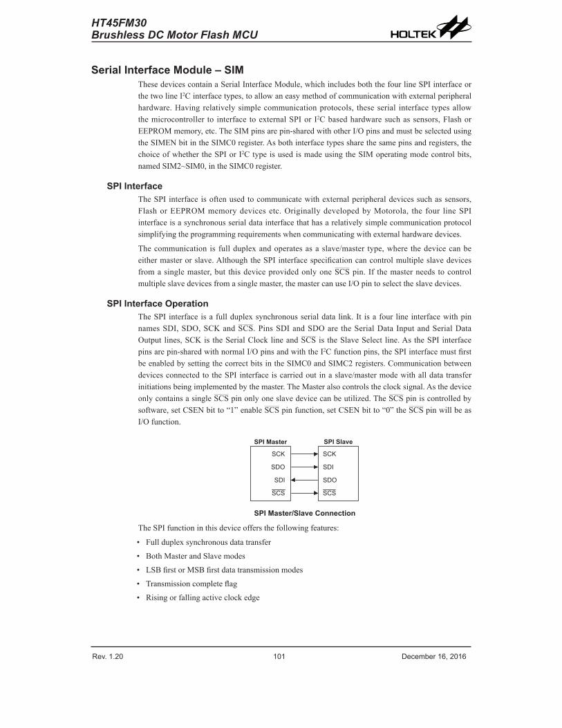
Rev. 1.20 100 De�e��e� 1�� 201� Rev. 1.20 101 De�e��e� 1�� 201�
HT45FM30Brushless DC Motor Flash MCU
Serial Interface Module – SIMThesedevicescontainaSerialInterfaceModule,whichincludesboththefourlineSPIinterfaceorthetwolineI2Cinterfacetypes,toallowaneasymethodofcommunicationwithexternalperipheralhardware.Havingrelativelysimplecommunicationprotocols, theseserial interface typesallowthemicrocontroller to interface toexternalSPIorI2Cbasedhardwaresuchassensors,FlashorEEPROMmemory,etc.TheSIMpinsarepin-sharedwithotherI/OpinsandmustbeselectedusingtheSIMENbitintheSIMC0register.Asbothinterfacetypessharethesamepinsandregisters,thechoiceofwhethertheSPIorI2CtypeisusedismadeusingtheSIMoperatingmodecontrolbits,namedSIM2~SIM0,intheSIMC0register.
SPI InterfaceTheSPIinterfaceisoftenusedtocommunicatewithexternalperipheraldevicessuchassensors,FlashorEEPROMmemorydevicesetc.OriginallydevelopedbyMotorola, the four lineSPIinterfaceisasynchronousserialdatainterfacethathasarelativelysimplecommunicationprotocolsimplifyingtheprogrammingrequirementswhencommunicatingwithexternalhardwaredevices.
Thecommunication isfullduplexandoperatesasaslave/master type,where thedevicecanbeeithermasterorslave.AlthoughtheSPIinterfacespecificationcancontrolmultipleslavedevicesfromasinglemaster,but thisdeviceprovidedonlyoneSCSpin.If themasterneeds tocontrolmultipleslavedevicesfromasinglemaster,themastercanuseI/Opintoselecttheslavedevices.
SPI Interface OperationTheSPIinterfaceisafullduplexsynchronousserialdatalink.It isafourlineinterfacewithpinnamesSDI,SDO,SCKandSCS.PinsSDIandSDOare theSerialDataInputandSerialDataOutput lines,SCKis theSerialClocklineandSCSis theSlaveSelect line.AstheSPIinterfacepinsarepin-sharedwithnormalI/OpinsandwiththeI2Cfunctionpins,theSPIinterfacemustfirstbeenabledbysettingthecorrectbitsintheSIMC0andSIMC2registers.CommunicationbetweendevicesconnectedtotheSPIinterfaceiscarriedoutinaslave/mastermodewithalldatatransferinitiationsbeingimplementedbythemaster.TheMasteralsocontrolstheclocksignal.AsthedeviceonlycontainsasingleSCSpinonlyoneslavedevicecanbeutilized.TheSCSpiniscontrolledbysoftware,setCSENbitto“1”enableSCSpinfunction,setCSENbitto“0”theSCSpinwillbeasI/Ofunction.
� � � � � � � � � � � � � � � � � � �
� � �
� � �
� � �
� � �
� � �
� � �
� � �
� � �
SPI Master/Slave Connection
TheSPIfunctioninthisdeviceoffersthefollowingfeatures:
• Fullduplexsynchronousdatatransfer
• BothMasterandSlavemodes
• LSBfirstorMSBfirstdatatransmissionmodes
• Transmissioncompleteflag
• Risingorfallingactiveclockedge
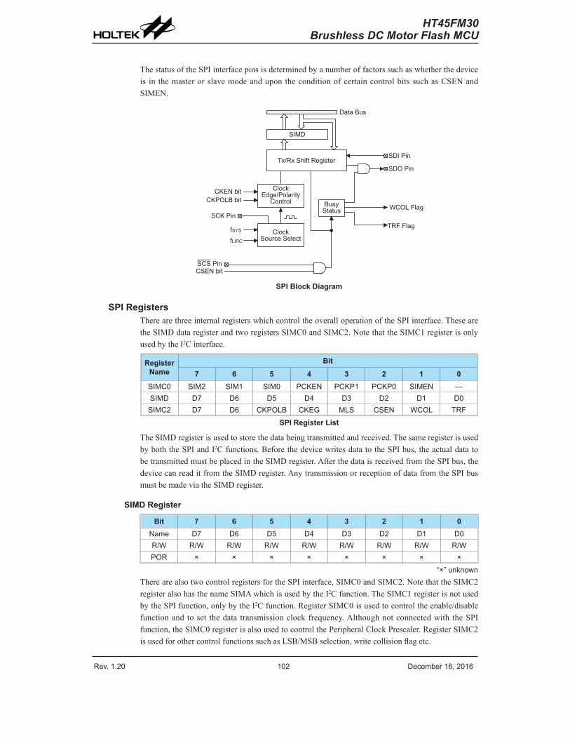
Rev. 1.20 102 De�e��e� 1�� 201� Rev. 1.20 103 De�e��e� 1�� 201�
HT45FM30Brushless DC Motor Flash MCU
ThestatusoftheSPIinterfacepinsisdeterminedbyanumberoffactorssuchaswhetherthedeviceis in themasterorslavemodeandupontheconditionofcertaincontrolbitssuchasCSENandSIMEN.
� � � � � � � �
� � � � � � �
� � � � � � �
� � � �
� � � � � � � � � � � � � � � � �
� � � �� � � � � �
� � � � � � �
� � � � � � � �
� � � � �� � � � � � � � � � �
� � � � � �
� � � � �� � � � � � � � � � � �
� � � �� � � � �
� � � � � � �
� � � � � � �� � � � � � �
� � � � � � �� � � � � � � � �
SPI Block Diagram
SPI RegistersTherearethreeinternalregisterswhichcontroltheoveralloperationoftheSPIinterface.ThesearetheSIMDdataregisterandtworegistersSIMC0andSIMC2.NotethattheSIMC1registerisonlyusedbytheI2Cinterface.
RegisterName
Bit
7 6 5 4 3 2 1 0SIMC0 SIM2 SIM1 SIM0 PCKEN PCKP1 PCKP0 SIMEN —SIMD D7 D� D5 D4 D3 D2 D1 D0SIMC2 D7 D� CKPOLB CKEG MLS CSEN WCOL TRF
SPI Register List
TheSIMDregisterisusedtostorethedatabeingtransmittedandreceived.ThesameregisterisusedbyboththeSPIandI2Cfunctions.BeforethedevicewritesdatatotheSPIbus,theactualdatatobetransmittedmustbeplacedintheSIMDregister.AfterthedataisreceivedfromtheSPIbus,thedevicecanreaditfromtheSIMDregister.AnytransmissionorreceptionofdatafromtheSPIbusmustbemadeviatheSIMDregister.
SIMD Register
Bit 7 6 5 4 3 2 1 0Na�e D7 D� D5 D4 D3 D2 D1 D0R/W R/W R/W R/W R/W R/W R/W R/W R/WPOR × × × × × × × ×
“×” unknownTherearealsotwocontrolregistersfortheSPIinterface,SIMC0andSIMC2.NotethattheSIMC2registeralsohasthenameSIMAwhichisusedbytheI2Cfunction.TheSIMC1registerisnotusedbytheSPIfunction,onlybytheI2Cfunction.RegisterSIMC0isusedtocontroltheenable/disablefunctionandtoset thedata transmissionclockfrequency.Althoughnotconnectedwith theSPIfunction,theSIMC0registerisalsousedtocontrolthePeripheralClockPrescaler.RegisterSIMC2isusedforothercontrolfunctionssuchasLSB/MSBselection,writecollisionflagetc.
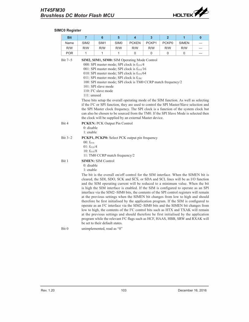
Rev. 1.20 102 De�e��e� 1�� 201� Rev. 1.20 103 De�e��e� 1�� 201�
HT45FM30Brushless DC Motor Flash MCU
SIMC0 Register
Bit 7 6 5 4 3 2 1 0Na�e SIM2 SIM1 SIM0 PCKEN PCKP1 PCKP0 SIMEN —R/W R/W R/W R/W R/W R/W R/W R/W —POR 1 1 1 0 0 0 0 —
Bit7~5 SIM2, SIM1, SIM0:SIMOperatingModeControl000:SPImastermode;SPIclockisfSYS/4001:SPImastermode;SPIclockisfSYS/16010:SPImastermode;SPIclockisfSYS/64011:SPImastermode;SPIclockisfLIRC100:SPImastermode;SPIclockisTM0CCRPmatchfrequency/2101:SPIslavemode110:I2Cslavemode111:unusedThesebitssetuptheoveralloperatingmodeoftheSIMfunction.AswellasselectingiftheI2CorSPIfunction,theyareusedtocontroltheSPIMaster/SlaveselectionandtheSPIMasterclockfrequency.TheSPIclockisafunctionofthesystemclockbutcanalsobechosentobesourcedfromtheTM0.IftheSPISlaveModeisselectedthentheclockwillbesuppliedbyanexternalMasterdevice.
Bit4 PCKEN:PCKOutputPinControl0:disable1:enable
Bit3~2 PCKP1, PCKP0:SelectPCKoutputpinfrequency00:fSYS01:fSYS/410:fSYS/811:TM0CCRPmatchfrequency/2
Bit1 SIMEN:SIMControl0:disable1:enableThebit is theoverallon/offcontrolfor theSIMinterface.WhentheSIMENbit iscleared,theSDI,SDO,SCKandSCS,orSDAandSCLlineswillbeasI/Ofunctionand theSIMoperatingcurrentwillbereduced toaminimumvalue.When thebitishightheSIMinterface isenabled.If theSIMisconfiguredtooperateasanSPIinterfaceviatheSIM2~SIM0bits,thecontentsoftheSPIcontrolregisterswillremainat theprevioussettingswhentheSIMENbitchangesfromlowtohighandshouldthereforebefirst initialisedbytheapplicationprogram.If theSIMisconfiguredtooperateasanI2CinterfaceviatheSIM2~SIM0bitsandtheSIMENbitchangesfromlowtohigh,thecontentsoftheI2CcontrolbitssuchasHTXandTXAKwillremainat theprevioussettingsandshould thereforebefirst initialisedby theapplicationprogramwhiletherelevantI2CflagssuchasHCF,HAAS,HBB,SRWandRXAKwillbesettotheirdefaultstates.
Bit0 unimplemented,readas“0”
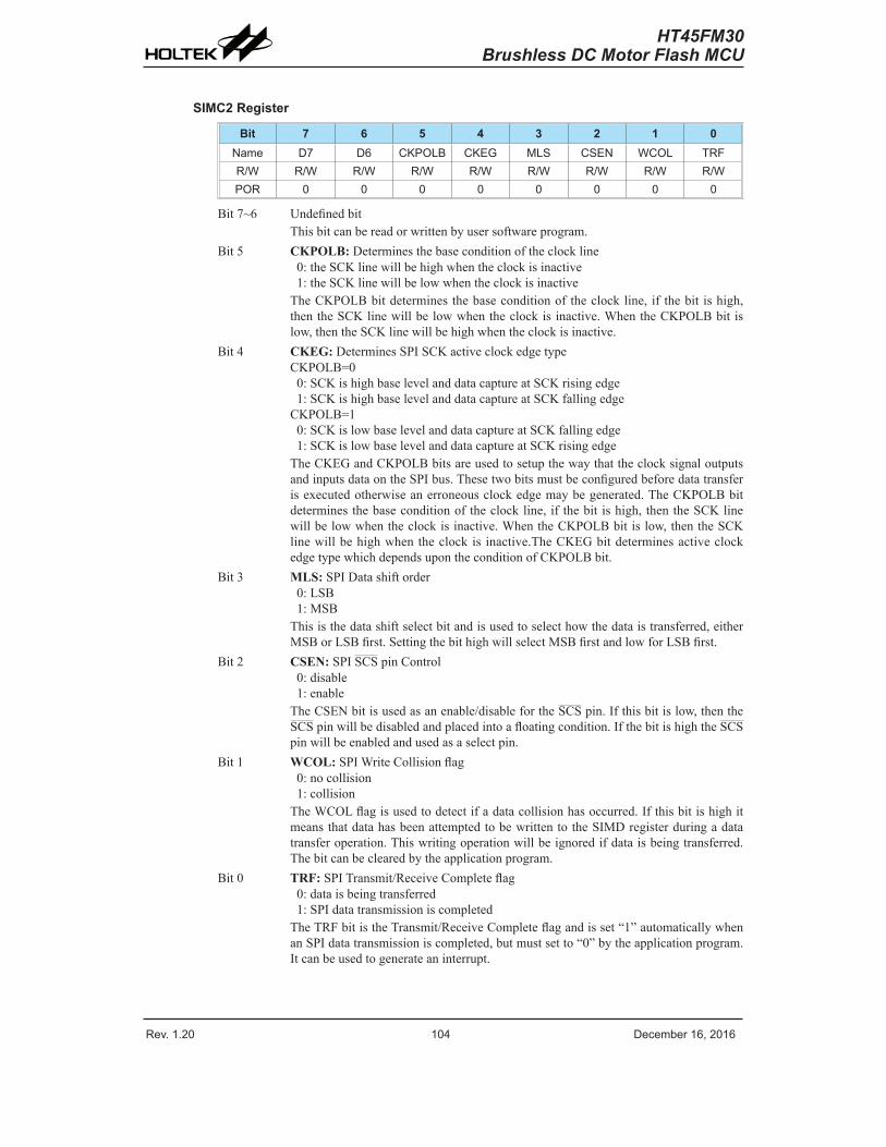
Rev. 1.20 104 De�e��e� 1�� 201� Rev. 1.20 105 De�e��e� 1�� 201�
HT45FM30Brushless DC Motor Flash MCU
SIMC2 Register
Bit 7 6 5 4 3 2 1 0Na�e D7 D� CKPOLB CKEG MLS CSEN WCOL TRFR/W R/W R/W R/W R/W R/W R/W R/W R/WPOR 0 0 0 0 0 0 0 0
Bit7~6 UndefinedbitThisbitcanbereadorwrittenbyusersoftwareprogram.
Bit5 CKPOLB:Determinesthebaseconditionoftheclockline0:theSCKlinewillbehighwhentheclockisinactive1:theSCKlinewillbelowwhentheclockisinactiveTheCKPOLBbitdeterminesthebaseconditionoftheclockline, if thebit ishigh,thentheSCKlinewillbelowwhentheclockisinactive.WhentheCKPOLBbitislow,thentheSCKlinewillbehighwhentheclockisinactive.
Bit4 CKEG:DeterminesSPISCKactiveclockedgetypeCKPOLB=00:SCKishighbaselevelanddatacaptureatSCKrisingedge1:SCKishighbaselevelanddatacaptureatSCKfallingedgeCKPOLB=10:SCKislowbaselevelanddatacaptureatSCKfallingedge1:SCKislowbaselevelanddatacaptureatSCKrisingedgeTheCKEGandCKPOLBbitsareusedtosetupthewaythattheclocksignaloutputsandinputsdataontheSPIbus.Thesetwobitsmustbeconfiguredbeforedatatransferisexecutedotherwiseanerroneousclockedgemaybegenerated.TheCKPOLBbitdeterminesthebaseconditionoftheclockline, if thebit ishigh,thentheSCKlinewillbelowwhentheclockisinactive.WhentheCKPOLBbitislow,thentheSCKlinewillbehighwhentheclockis inactive.TheCKEGbitdeterminesactiveclockedgetypewhichdependsupontheconditionofCKPOLBbit.
Bit3 MLS:SPIDatashiftorder0:LSB1:MSBThisisthedatashiftselectbitandisusedtoselecthowthedataistransferred,eitherMSBorLSBfirst.SettingthebithighwillselectMSBfirstandlowforLSBfirst.
Bit2 CSEN:SPISCSpinControl0:disable1:enableTheCSENbitisusedasanenable/disablefortheSCSpin.Ifthisbitislow,thentheSCSpinwillbedisabledandplacedintoafloatingcondition.IfthebitishightheSCSpinwillbeenabledandusedasaselectpin.
Bit1 WCOL:SPIWriteCollisionflag0:nocollision1:collisionTheWCOLflagisusedtodetectifadatacollisionhasoccurred.IfthisbitishighitmeansthatdatahasbeenattemptedtobewrittentotheSIMDregisterduringadatatransferoperation.Thiswritingoperationwillbeignoredifdataisbeingtransferred.Thebitcanbeclearedbytheapplicationprogram.
Bit0 TRF:SPITransmit/ReceiveCompleteflag0:dataisbeingtransferred1:SPIdatatransmissioniscompletedTheTRFbitistheTransmit/ReceiveCompleteflagandisset“1”automaticallywhenanSPIdatatransmissioniscompleted,butmustsetto“0”bytheapplicationprogram.Itcanbeusedtogenerateaninterrupt.
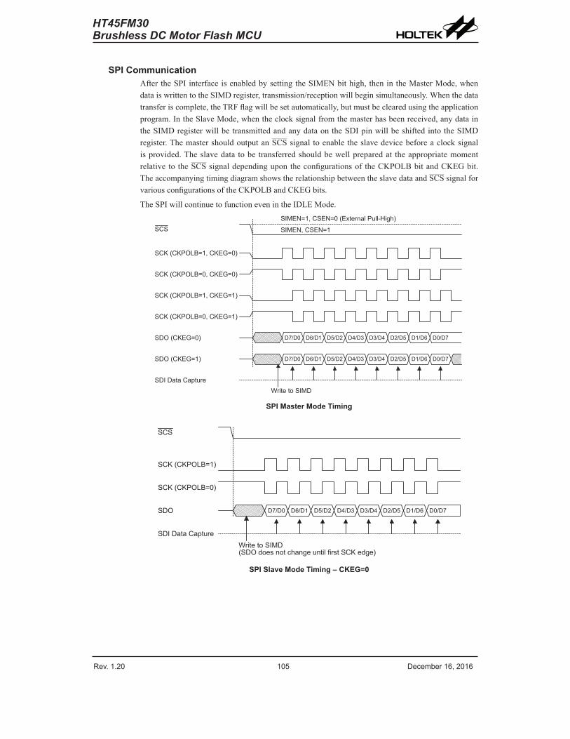
Rev. 1.20 104 De�e��e� 1�� 201� Rev. 1.20 105 De�e��e� 1�� 201�
HT45FM30Brushless DC Motor Flash MCU
SPI CommunicationAftertheSPIinterfaceisenabledbysettingtheSIMENbithigh,thenintheMasterMode,whendataiswrittentotheSIMDregister,transmission/receptionwillbeginsimultaneously.Whenthedatatransferiscomplete,theTRFflagwillbesetautomatically,butmustbeclearedusingtheapplicationprogram.IntheSlaveMode,whentheclocksignalfromthemasterhasbeenreceived,anydataintheSIMDregisterwillbetransmittedandanydataontheSDIpinwillbeshiftedintotheSIMDregister.ThemastershouldoutputanSCSsignal toenabletheslavedevicebeforeaclocksignalisprovided.Theslavedata tobetransferredshouldbewellpreparedat theappropriatemomentrelativetotheSCSsignaldependingupontheconfigurationsoftheCKPOLBbitandCKEGbit.TheaccompanyingtimingdiagramshowstherelationshipbetweentheslavedataandSCSsignalforvariousconfigurationsoftheCKPOLBandCKEGbits.
TheSPIwillcontinuetofunctionevenintheIDLEMode.
� � � � � � � � � � � � � � � � � � � � � �
� � � � � � � � � � �
� � � � � � � � � � � � � � � � � � � � � � � � � � � � � � � �
� � � � � � � � � � � � � � � � � � � � � �
� � � � � � � � � � � � � � � � � � � � � �
� � � � � � � � � � � � � � � � � � � � � �
� � � � � � � � � � � �
� � � � � � � � � � � �
� � �
� � � � � � � � � � � � � �
� � � � � � � � � � � � � � � � � � � � � � � � � � � � � � � � � � � �
� � � � � � � � � � � � � � � � � � � � � � � � � � � � � � � � � � � �
� � � � � � � � � � �
SPI Master Mode Timing
� � � � � � � � � � � � � �
� � � � � � � � � � � � � �
� � �
� � �
� � � � � � � � � � � � � � �
� � � � � � � � � � � � � � � � � � � � � � � � � � � � � �
� � � � � � � � � � � � �� � � � � � � � � � � � � � � � � � � � � � � � � � � � � � � � � � � � � �
SPI Slave Mode Timing – CKEG=0
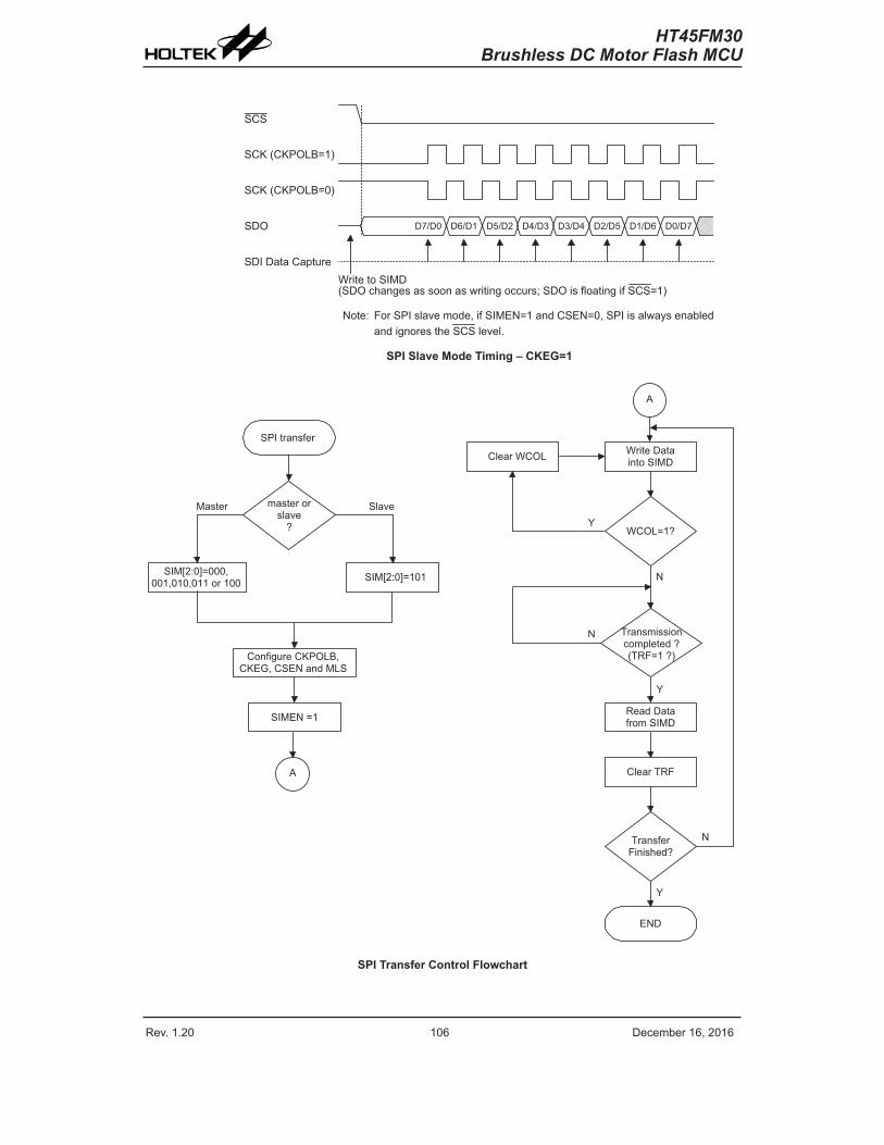
Rev. 1.20 10� De�e��e� 1�� 201� Rev. 1.20 107 De�e��e� 1�� 201�
HT45FM30Brushless DC Motor Flash MCU
� � � � � � � � � � � � � �
� � � � � � � � � � � � � �
� � �
� � �
� � � � � � � � � � � � � � �
� � � � � � � � � � � � � � � � � � � � � � � � � � � � � �
� � � � � � � � � � � � �� � � � � � � � � � � � � � � � � � � � � � � � � � � � � � � � � � � � � � � � � � � � � � � � � � � � � � � � � � � � � �
� � � � � � � � � � � � � � � � � � � � � � � � � � � � � � � � � � � � � � � � � � � � � � � � � � � � � � � � � � � � � � � � � � � �� � � � � � � � � � � � � � � � � � � � � � � � � �
SPI Slave Mode Timing – CKEG=1
� � � � � � � �
� � � � � � � � � �� � � � � � � � �
� � � � � �
� � � � � � � �
� � � � � � � � � � � �� � � � � � � � � �� � � � � � � � � �
�
� � � � � � � � �� � � � � � � � �
� � � � � � � �
� � � � � � � �� � � � � � � � �
�
� � �
� � � � � � � � �� � � ��
� � � � � � � � � �
�
� � � � � � � � � � � �
� � � � � � � � � � � � � �� � � � � � � � � � � � � � � � � � �
� � � � � � � � � � � � �� � � � � � � � � � � � � � � � � � � � � � � � � � � � � � � �
�
SPI Transfer Control Flowchart
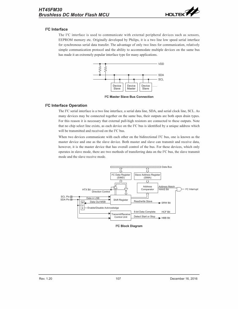
Rev. 1.20 10� De�e��e� 1�� 201� Rev. 1.20 107 De�e��e� 1�� 201�
HT45FM30Brushless DC Motor Flash MCU
I2C InterfaceThe I2C interface isused to communicatewith externalperipheraldevices suchas sensors,EEPROMmemoryetc.OriginallydevelopedbyPhilips,it isatwolinelowspeedserialinterfaceforsynchronousserialdatatransfer.Theadvantageofonlytwolinesforcommunication,relativelysimplecommunicationprotocolandtheabilitytoaccommodatemultipledevicesonthesamebushasmadeitanextremelypopularinterfacetypeformanyapplications.
� � � � � �� � � � �
� � � � � �� � � � � �
� � � � � �� � � � �
� � �
� � �� � �
I2C Master Slave Bus Connection
I2C Interface OperationTheI2Cserialinterfaceisatwolineinterface,aserialdataline,SDA,andserialclockline,SCL.Asmanydevicesmaybeconnectedtogetheronthesamebus,theiroutputsarebothopendraintypes.Forthisreasonitisnecessarythatexternalpull-highresistorsareconnectedtotheseoutputs.Notethatnochipselectlineexists,aseachdeviceontheI2CbusisidentifiedbyauniqueaddresswhichwillbetransmittedandreceivedontheI2Cbus.
WhentwodevicescommunicatewitheachotheronthebidirectionalI2Cbus,oneisknownasthemasterdeviceandoneas theslavedevice.Bothmasterandslavecantransmitandreceivedata,however, it isthemasterdevicethathasoverallcontrolofthebus.Forthesedevices,whichonlyoperatesinslavemode,therearetwomethodsoftransferringdataontheI2Cbus,theslavetransmitmodeandtheslavereceivemode.
� � � � � � � � � � � � � � � � �� � � � � �
� � � � � � � � � � � � � � � � � � � � �� � � � � �
� � � � � � � � � � � �
� � � � � � � � � � � � � � � � �
���
� � � � � � � � � � � � � � � � � � � � � � � � � � � � � � � � �
� � � � � � � � � � �� � � � � � � � � � � �
� � � � � � � � � � � � � � �� � � � � � � � � � � �
� � � � � � � � � � � � � � � � �
� � � � � � � � � � � � � � � � � � � �
� � � � � � � �
� � � � � � �� � � � � � � � � �
� � � � � � � � � � � � � � � � � � � � � � � � � �
� � � � � � � � � � � � � � � � � � � � � �
� � � � � � �
� � � � � � �
� � � � � � �� � � � � � �
� � � � � � �
I2C Block Diagram
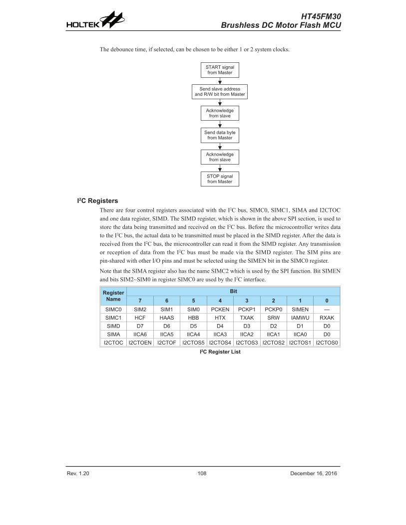
Rev. 1.20 108 De�e��e� 1�� 201� Rev. 1.20 109 De�e��e� 1�� 201�
HT45FM30Brushless DC Motor Flash MCU
Thedebouncetime,ifselected,canbechosentobeeither1or2systemclocks.
� � � � � � � � � � � �� � � � � � � � � � �
� � � � � � � � � � � � � � �� � � � � � � � � � � � � � � � � � � �
� � � � � � � � � �� � � � � � � � � �
� � � � � � � � � � �� � � � � � � � � � �
� � � � � � � � � �� � � � � � � � � �
� � � � � � � � � � �� � � � � � � � � � �
I2C RegistersTherearefourcontrolregistersassociatedwiththeI2Cbus,SIMC0,SIMC1,SIMAandI2CTOCandonedataregister,SIMD.TheSIMDregister,whichisshownintheaboveSPIsection,isusedtostorethedatabeingtransmittedandreceivedontheI2Cbus.BeforethemicrocontrollerwritesdatatotheI2Cbus,theactualdatatobetransmittedmustbeplacedintheSIMDregister.AfterthedataisreceivedfromtheI2Cbus,themicrocontrollercanreaditfromtheSIMDregister.Anytransmissionor receptionofdata fromthe I2Cbusmustbemadevia theSIMDregister.TheSIMpinsarepin-sharedwithotherI/OpinsandmustbeselectedusingtheSIMENbitintheSIMC0register.
NotethattheSIMAregisteralsohasthenameSIMC2whichisusedbytheSPIfunction.BitSIMENandbitsSIM2~SIM0inregisterSIMC0areusedbytheI2Cinterface.
RegisterName
Bit
7 6 5 4 3 2 1 0SIMC0 SIM2 SIM1 SIM0 PCKEN PCKP1 PCKP0 SIMEN —SIMC1 HCF HAAS HBB HTX TXAK SRW IAMWU RXAKSIMD D7 D� D5 D4 D3 D2 D1 D0SIMA IICA� IICA5 IICA4 IICA3 IICA2 IICA1 IICA0 D0
I2CTOC I2CTOEN I2CTOF I2CTOS5 I2CTOS4 I2CTOS3 I2CTOS2 I2CTOS1 I2CTOS0
I2C Register List
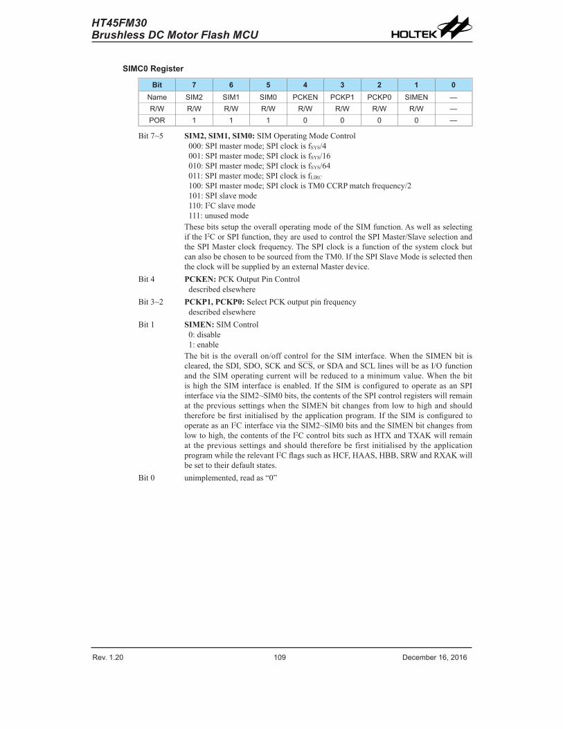
Rev. 1.20 108 De�e��e� 1�� 201� Rev. 1.20 109 De�e��e� 1�� 201�
HT45FM30Brushless DC Motor Flash MCU
SIMC0 Register
Bit 7 6 5 4 3 2 1 0Na�e SIM2 SIM1 SIM0 PCKEN PCKP1 PCKP0 SIMEN —R/W R/W R/W R/W R/W R/W R/W R/W —POR 1 1 1 0 0 0 0 —
Bit7~5 SIM2, SIM1, SIM0:SIMOperatingModeControl000:SPImastermode;SPIclockisfSYS/4001:SPImastermode;SPIclockisfSYS/16010:SPImastermode;SPIclockisfSYS/64011:SPImastermode;SPIclockisfLIRC100:SPImastermode;SPIclockisTM0CCRPmatchfrequency/2101:SPIslavemode110:I2Cslavemode111:unusedmodeThesebitssetuptheoveralloperatingmodeoftheSIMfunction.AswellasselectingiftheI2CorSPIfunction,theyareusedtocontroltheSPIMaster/SlaveselectionandtheSPIMasterclockfrequency.TheSPIclockisafunctionofthesystemclockbutcanalsobechosentobesourcedfromtheTM0.IftheSPISlaveModeisselectedthentheclockwillbesuppliedbyanexternalMasterdevice.
Bit4 PCKEN:PCKOutputPinControldescribedelsewhere
Bit3~2 PCKP1, PCKP0:SelectPCKoutputpinfrequencydescribedelsewhere
Bit1 SIMEN:SIMControl0:disable1:enableThebit is theoverallon/offcontrolfor theSIMinterface.WhentheSIMENbit iscleared,theSDI,SDO,SCKandSCS,orSDAandSCLlineswillbeasI/Ofunctionand theSIMoperatingcurrentwillbereduced toaminimumvalue.When thebitishightheSIMinterface isenabled.If theSIMisconfiguredtooperateasanSPIinterfaceviatheSIM2~SIM0bits,thecontentsoftheSPIcontrolregisterswillremainat theprevioussettingswhentheSIMENbitchangesfromlowtohighandshouldthereforebefirst initialisedbytheapplicationprogram.If theSIMisconfiguredtooperateasanI2CinterfaceviatheSIM2~SIM0bitsandtheSIMENbitchangesfromlowtohigh,thecontentsoftheI2CcontrolbitssuchasHTXandTXAKwillremainat theprevioussettingsandshould thereforebefirst initialisedby theapplicationprogramwhiletherelevantI2CflagssuchasHCF,HAAS,HBB,SRWandRXAKwillbesettotheirdefaultstates.
Bit0 unimplemented,readas“0”
Rev. 1.20 110 De�e��e� 1�� 201� Rev. 1.20 111 De�e��e� 1�� 201�
HT45FM30Brushless DC Motor Flash MCU
SIMC1 Register
Bit 7 6 5 4 3 2 1 0Na�e HCF HAAS HBB HTX TXAK SRW IAMWU RXAKR/W R R R R/W R/W R R/W RPOR 1 0 0 0 0 0 0 1
Bit7 HCF:I2CBusdatatransfercompletionflag0:dataisbeingtransferred1:completionofan8-bitdatatransferTheHCFflag is thedata transfer flag.This flagwillbezerowhendata isbeingtransferred.Uponcompletionofan8-bitdatatransfertheflagwillgohighandaninterruptwillbegenerated.
Bit6 HAAS:I2CBusaddressmatchflag0:notaddressmatch1:addressmatchTheHASSflagistheaddressmatchflag.Thisflagisusedtodetermineif theslavedeviceaddressisthesameasthemastertransmitaddress.Iftheaddressesmatchthenthisbitwillbehigh,ifthereisnomatchthentheflagwillbelow.
Bit5 HBB:I2CBusbusyflag0:I2CBusisnotbusy1:I2CBusisbusyTheHBBflagis theI2Cbusyflag.Thisflagwillbe“1”whentheI2Cbus isbusywhichwilloccurwhenaSTARTsignalisdetected.Theflagwillbesetto“0”whenthebusisfreewhichwilloccurwhenaSTOPsignalisdetected.
Bit4 HTX:SelectI2Cslavedeviceistransmitterorreceiver0:slavedeviceisthereceiver1:slavedeviceisthetransmitter
Bit3 TXAK:I2CBustransmitacknowledgeflag0:slavesendacknowledgeflag1:slavedonotsendacknowledgeflagTheTXAKbitisthetransmitacknowledgeflag.Aftertheslavedevicereceiptof8-bitsofdata,thisbitwillbetransmittedtothebusonthe9thclockfromtheslavedevice.TheslavedevicemustalwayssetTXAKbitto“0”beforefurtherdataisreceived.
Bit2 SRW:I2CSlaveRead/Writeflag0:slavedeviceshouldbeinreceivemode1:slavedeviceshouldbeintransmitmodeTheSRWflag is the I2CSlaveRead/Write flag.This flagdetermineswhetherthemasterdevicewishes to transmitor receivedata fromthe I2Cbus.When thetransmittedaddressandslaveaddressismatch,thatiswhentheHAASflagissethigh,theslavedevicewillchecktheSRWflagtodeterminewhetheritshouldbeintransmitmodeorreceivemode.IftheSRWflagishigh,themasterisrequestingtoreaddatafromthebus,so theslavedeviceshouldbe in transmitmode.WhentheSRWflagiszero,themasterwillwritedatatothebus,thereforetheslavedeviceshouldbeinreceivemodetoreadthisdata.
Bit1 IAMWU:I2Caddressmatchwake-upcontrol0:disable1:enableThisbitshouldbeset to“1”toenableI2Caddressmatchwake-upfromSLEEPorIDLEMode.
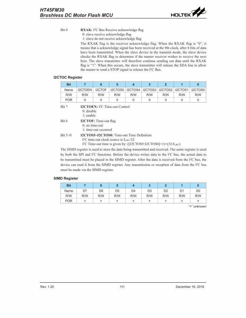
Rev. 1.20 110 De�e��e� 1�� 201� Rev. 1.20 111 De�e��e� 1�� 201�
HT45FM30Brushless DC Motor Flash MCU
Bit0 RXAK:I2CBusReceiveacknowledgeflag0:slavereceiveacknowledgeflag1:slavedonotreceiveacknowledgeflagTheRXAKflag is thereceiveracknowledgeflag.WhentheRXAKflag is“0”, itmeansthataacknowledgesignalhasbeenreceivedatthe9thclock,after8bitsofdatahavebeentransmitted.Whentheslavedeviceinthetransmitmode,theslavedevicecheckstheRXAKflagtodetermineifthemasterreceiverwishestoreceivethenextbyte.Theslavetransmitterwill thereforecontinuesendingoutdatauntil theRXAKflagis“1”.Whenthisoccurs,theslavetransmitterwillreleasetheSDAlinetoallowthemastertosendaSTOPsignaltoreleasetheI2CBus.
I2CTOC Register
Bit 7 6 5 4 3 2 1 0Na�e I2CTOEN I2CTOF I2CTOS5 I2CTOS4 I2CTOS3 I2CTOS2 I2CTOS1 I2CTOS0R/W R/W R/W R/W R/W R/W R/W R/W R/WPOR 0 0 0 0 0 0 0 0
Bit7 I2CTOEN:I2CTime-outControl0:disable1:enable
Bit6 I2CTOF: Time-outflag0:notime-out1:time-outoccurred
Bit5~0 I2CTOS5~I2CTOS0:Time-outTimeDefinitionI2Ctime-outclocksourceisfLIRC/32I2CTime-outtimeisgivenby:([I2CTOS5:I2CTOS0]+1)×(32/fLIRC)
TheSIMDregisterisusedtostorethedatabeingtransmittedandreceived.ThesameregisterisusedbyboththeSPIandI2Cfunctions.BeforethedevicewritesdatatotheI2Cbus,theactualdatatobetransmittedmustbeplacedintheSIMDregister.AfterthedataisreceivedfromtheI2Cbus,thedevicecanreaditfromtheSIMDregister.AnytransmissionorreceptionofdatafromtheI2CbusmustbemadeviatheSIMDregister.
SIMD Register
Bit 7 6 5 4 3 2 1 0Na�e D7 D� D5 D4 D3 D2 D1 D0R/W R/W R/W R/W R/W R/W R/W R/W R/WPOR × × × × × × × ×
“×” unknown
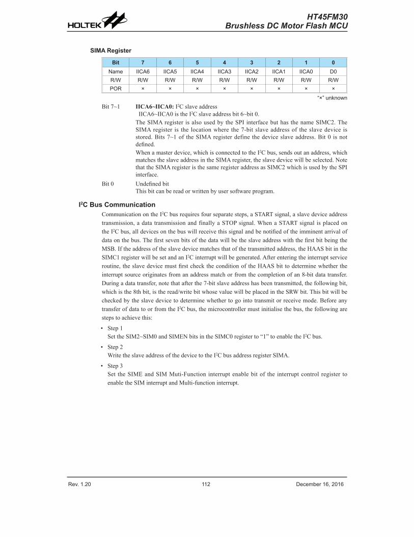
Rev. 1.20 112 De�e��e� 1�� 201� Rev. 1.20 113 De�e��e� 1�� 201�
HT45FM30Brushless DC Motor Flash MCU
SIMA Register
Bit 7 6 5 4 3 2 1 0Na�e IICA� IICA5 IICA4 IICA3 IICA2 IICA1 IICA0 D0R/W R/W R/W R/W R/W R/W R/W R/W R/WPOR × × × × × × × ×
“×” unknownBit7~1 IICA6~IICA0:I2Cslaveaddress
IICA6~IICA0istheI2Cslaveaddressbit6~bit0.TheSIMAregister isalsousedbytheSPI interfacebuthas thenameSIMC2.TheSIMAregister is the locationwhere the7-bitslaveaddressof theslavedevice isstored.Bits7~1of theSIMAregisterdefine thedeviceslaveaddress.Bit0 isnotdefined.Whenamasterdevice,whichisconnectedtotheI2Cbus,sendsoutanaddress,whichmatchestheslaveaddressintheSIMAregister,theslavedevicewillbeselected.NotethattheSIMAregisteristhesameregisteraddressasSIMC2whichisusedbytheSPIinterface.
Bit0 UndefinedbitThisbitcanbereadorwrittenbyusersoftwareprogram.
I2C Bus CommunicationCommunicationontheI2Cbusrequiresfourseparatesteps,aSTARTsignal,aslavedeviceaddresstransmission,adatatransmissionandfinallyaSTOPsignal.WhenaSTARTsignal isplacedontheI2Cbus,alldevicesonthebuswillreceivethissignalandbenotifiedoftheimminentarrivalofdataonthebus.ThefirstsevenbitsofthedatawillbetheslaveaddresswiththefirstbitbeingtheMSB.Iftheaddressoftheslavedevicematchesthatofthetransmittedaddress,theHAASbitintheSIMC1registerwillbesetandanI2Cinterruptwillbegenerated.Afterenteringtheinterruptserviceroutine,theslavedevicemustfirstchecktheconditionoftheHAASbittodeterminewhethertheinterruptsourceoriginatesfromanaddressmatchorfromthecompletionofan8-bitdatatransfer.Duringadatatransfer,notethatafterthe7-bitslaveaddresshasbeentransmitted,thefollowingbit,whichisthe8thbit,istheread/writebitwhosevaluewillbeplacedintheSRWbit.Thisbitwillbecheckedbytheslavedevicetodeterminewhethertogointotransmitorreceivemode.BeforeanytransferofdatatoorfromtheI2Cbus,themicrocontrollermustinitialisethebus,thefollowingarestepstoachievethis:
• Step1SettheSIM2~SIM0andSIMENbitsintheSIMC0registerto“1”toenabletheI2Cbus.
• Step2WritetheslaveaddressofthedevicetotheI2CbusaddressregisterSIMA.
• Step3Set theSIMEandSIMMuti-Function interruptenablebitof the interruptcontrol register toenabletheSIMinterruptandMulti-functioninterrupt.
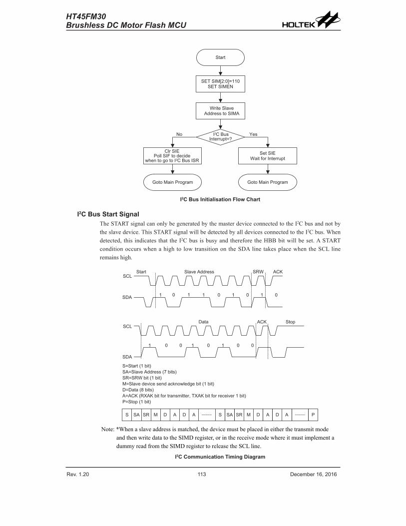
Rev. 1.20 112 De�e��e� 1�� 201� Rev. 1.20 113 De�e��e� 1�� 201�
HT45FM30Brushless DC Motor Flash MCU
� � � � �
� � � � � � � � � � � � �� � � � � � � � � � � � � � � � �
� � � � � � � � � � � � � � � � � � � � �
� � � � � � � � � �� � � � � � � � � � �
�
� � �� �
� � � � � � �� � � � � � � � � � � � � � � � � �
� � � � � � � � � � � � � � � �
� � � � � � � �� � � � � � � � � � � � � � � � � �
� � � � � � � � � � � � � � � � � � � � � � � � � �
� � � � � � � � � � � � � � � �
I2C Bus Initialisation Flow Chart
I2C Bus Start SignalTheSTARTsignalcanonlybegeneratedbythemasterdeviceconnectedtotheI2Cbusandnotbytheslavedevice.ThisSTARTsignalwillbedetectedbyalldevicesconnectedtotheI2Cbus.Whendetected, this indicates that theI2Cbus isbusyandtherefore theHBBbitwillbeset.ASTARTconditionoccurswhenahigh to lowtransitionon theSDAline takesplacewhentheSCLlineremainshigh.
� � � �
� � � � � � � � � �� � � � � � � � � � ��
� � � � � � �� �
� � � � � � � � � � � � � � �� � � � � � � � � � � � � � � � � � � � � �� � � � � � � � � � � � � � � � � � � � � � � � � � � � � � � � � � � � � � � � � � � � � � � � � � � � � � � � � �� � � � � � � � � � � � � �� � � � � � � � � � � � � � � � � � � � � � � � � � � � � � � � � � � � � � � � � � � � � � � � � � � � � � � � � � � � � � � � � � � � � � � �
� � �� � � � �
� � �
� � � � �
� � � � � � � � �
� � �
� � � � � � � � � � �
� � � � � � � � � � � � � � � � � �
Note:*Whenaslaveaddressismatched,thedevicemustbeplacedineitherthetransmitmodeandthenwritedatatotheSIMDregister,orinthereceivemodewhereitmustimplementadummyreadfromtheSIMDregistertoreleasetheSCLline.
I2C Communication Timing Diagram
Rev. 1.20 114 De�e��e� 1�� 201� Rev. 1.20 115 De�e��e� 1�� 201�
HT45FM30Brushless DC Motor Flash MCU
Slave AddressThetransmissionofaSTARTsignalbythemasterwillbedetectedbyalldevicesontheI2Cbus.Todeterminewhichslavedevicethemasterwishestocommunicatewith,theaddressoftheslavedevicewillbesentoutimmediatelyfollowingtheSTARTsignal.Allslavedevices,afterreceivingthis7-bitaddressdata,willcompareitwiththeirown7-bitslaveaddress.Iftheaddresssentoutbythemastermatchestheinternaladdressofthemicrocontrollerslavedevice,thenaninternalI2Cbusinterruptsignalwillbegenerated.Thenextbitfollowingtheaddress,whichisthe8thbit,definestheread/writestatusandwillbesavedtotheSRWbitoftheSIMC1register.Theslavedevicewillthentransmitanacknowledgebit,whichisalowlevel,asthe9thbit.TheslavedevicewillalsosetthestatusflagHAASwhentheaddressesmatch.
Asan I2Cbus interrupt cancome from two sources,when theprogramenters the interruptsubroutine,theHAASbitshouldbeexaminedtoseewhethertheinterruptsourcehascomefromamatchingslaveaddressorfromthecompletionofadatabytetransfer.Whenaslaveaddressismatched, thedevicemustbeplacedineither thetransmitmodeandthenwritedatatotheSIMDregister,orinthereceivemodewhereitmustimplementadummyreadfromtheSIMDregistertoreleasetheSCLline.
I2C Bus Read/Write SignalTheSRWbitintheSIMC1registerdefineswhethertheslavedevicewishestoreaddatafromtheI2CbusorwritedatatotheI2Cbus.Theslavedeviceshouldexaminethisbittodetermineifitistobeatransmitterorareceiver.IftheSRWflagis“1”thenthisindicatesthatthemasterdevicewishestoreaddatafromtheI2Cbus,thereforetheslavedevicemustbesetuptosenddatatotheI2Cbusasatransmitter.IftheSRWflagis“0”thenthisindicatesthatthemasterwishestosenddatatotheI2Cbus,thereforetheslavedevicemustbesetuptoreaddatafromtheI2Cbusasareceiver.
I2C Bus Slave Address Acknowledge SignalAfter themasterhas transmitted a calling address, any slavedeviceon the I2Cbus,whoseown internaladdressmatches thecallingaddress,mustgenerateanacknowledgesignal.Theacknowledgesignalwillinformthemasterthataslavedevicehasaccepteditscallingaddress.IfnoacknowledgesignalisreceivedbythemasterthenaSTOPsignalmustbetransmittedbythemastertoendthecommunication.WhentheHAASflagishigh,theaddresseshavematchedandtheslavedevicemustchecktheSRWflagtodetermineifitistobeatransmitterorareceiver.IftheSRWflagishigh,theslavedeviceshouldbesetuptobeatransmittersotheHTXbitintheSIMC1registershouldbesetto“1”.IftheSRWflagislow,thenthemicrocontrollerslavedeviceshouldbesetupasareceiverandtheHTXbitintheSIMC1registershouldbesetto“0”.
I2C Bus Data and Acknowledge SignalThetransmitteddatais8-bitswideandistransmittedaftertheslavedevicehasacknowledgedreceiptof itsslaveaddress.Theorderofserialbit transmissionis theMSBfirstandtheLSBlast.Afterreceiptof8-bitsofdata,thereceivermusttransmitanacknowledgesignal,level“0”,beforeitcanreceivethenextdatabyte.Iftheslavetransmitterdoesnotreceiveanacknowledgebitsignalfromthemasterreceiver,thentheslavetransmitterwillreleasetheSDAlinetoallowthemastertosendaSTOPsignaltoreleasetheI2CBus.ThecorrespondingdatawillbestoredintheSIMDregister.Ifsetupasatransmitter,theslavedevicemustfirstwritethedatatobetransmittedintotheSIMDregister.Ifsetupasareceiver,theslavedevicemustreadthetransmitteddatafromtheSIMDregister.
Whentheslavereceiver receives thedatabyte, itmustgenerateanacknowledgebit,knownasTXAK,onthe9thclock.Theslavedevice,whichissetupasatransmitterwillchecktheRXAKbitintheSIMC1registertodetermineifit istosendanotherdatabyte,ifnotthenitwillreleasetheSDAlineandawaitthereceiptofaSTOPsignalfromthemaster.
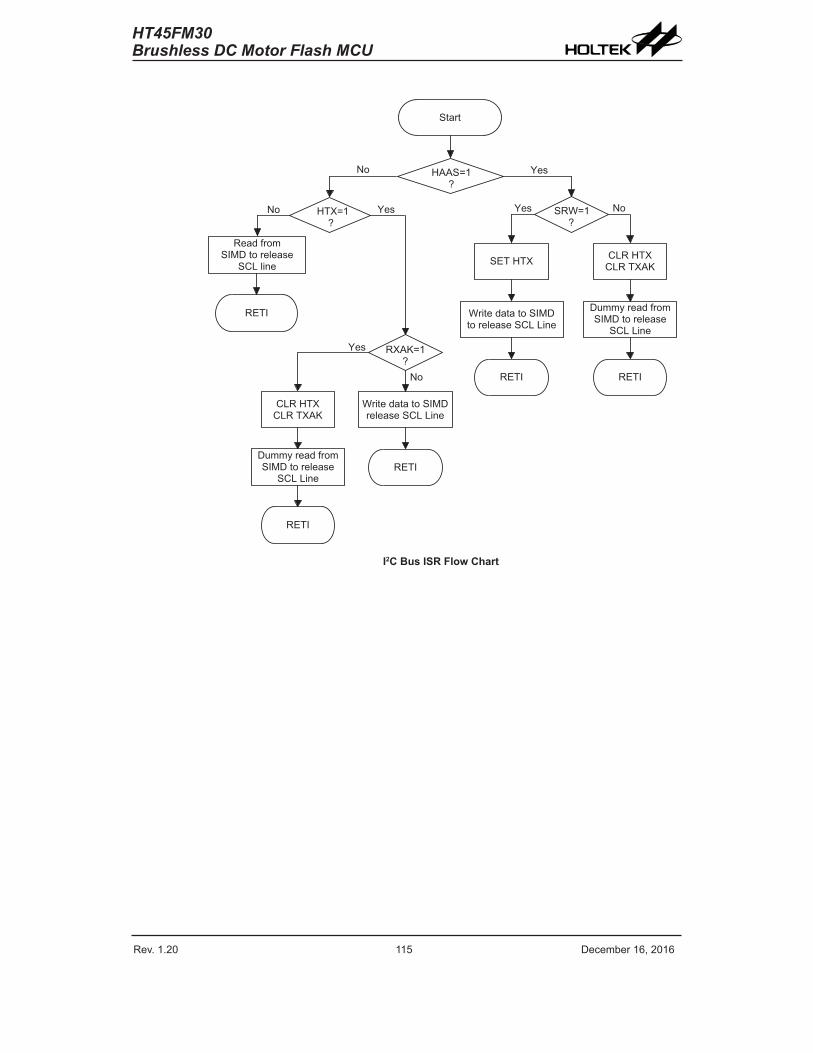
Rev. 1.20 114 De�e��e� 1�� 201� Rev. 1.20 115 De�e��e� 1�� 201�
HT45FM30Brushless DC Motor Flash MCU
� � � � �
� � � � � ��
� � � � �� � � � �
� � � � �� � � � � �
� � ��
� � � �
� � � � � ��
� � �
�
�
� � � � � � � � � � � � � � � � � � � �
� � � � � � � �
� � � �
� � �
� � � � � � � � � � � � � � � � � � � � � � � �
� � � � � � � �
� � � �
� � � �
� � � � � � � � � � � � � � � � �� � � � � � � � � � � � � � � �
� � � � � � �
� � � � � � � � � � � � � � � � �� � � � � � � � � � � � � � � � � �
� � � �
� � � � � � �� � � � � � � �
� � � � � � � � � � � � � � � � � � � � � � � �
� � � � � � � �
� � � � � � �� � � � � � � �
� � � �
I2C Bus ISR Flow Chart
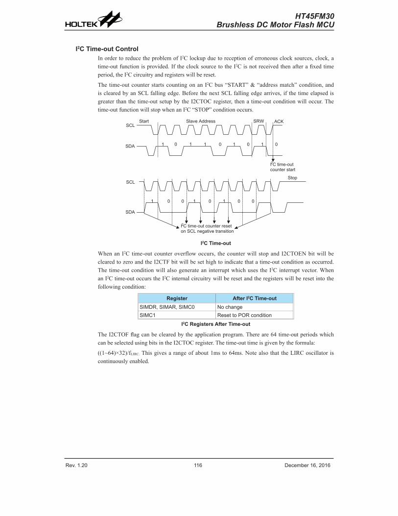
Rev. 1.20 11� De�e��e� 1�� 201� Rev. 1.20 117 De�e��e� 1�� 201�
HT45FM30Brushless DC Motor Flash MCU
I2C Time-out ControlInordertoreducetheproblemofI2Clockupduetoreceptionoferroneousclocksources,clock,atime-outfunctionisprovided.IftheclocksourcetotheI2Cisnotreceivedthenafterafixedtimeperiod,theI2Ccircuitryandregisterswillbereset.
Thetime-outcounterstartscountingonanI2Cbus“START”&“addressmatch”condition,andisclearedbyanSCLfallingedge.BeforethenextSCLfallingedgearrives,ifthetimeelapsedisgreater thanthetime-outsetupbytheI2CTOCregister, thenatime-outconditionwilloccur.Thetime-outfunctionwillstopwhenanI2C“STOP”conditionoccurs.
� � � � � � � � � � � �� � � � � � � � � � � � �
� � � � � � � � � � � � � � � � � � � � � � � � � �� � � � � � � � � � � � � � � � � � � � � � � � �
� � � � � � � � � �� � � � � � � � � � ��
� � � � � � �� �
� � �� � � � �
�
� � � � �
� � � �� � �
�
� � � � � � � � � � �
�
�
I2C Time-out
WhenanI2Ctime-outcounteroverflowoccurs, thecounterwillstopandI2CTOENbitwillbeclearedtozeroandtheI2CTFbitwillbesethightoindicatethatatime-outconditionasoccurred.Thetime-outconditionwillalsogenerateaninterruptwhichuses theI2Cinterruptvector.WhenanI2Ctime-outoccurstheI2Cinternalcircuitrywillberesetandtheregisterswillberesetintothefollowingcondition:
Register After I2C Time-outSIMDR� SIMAR� SIMC0 No �hangeSIMC1 Reset to POR �ondition
I2C Registers After Time-out
TheI2CTOFflagcanbeclearedbytheapplicationprogram.Thereare64time-outperiodswhichcanbeselectedusingbitsintheI2CTOCregister.Thetime-outtimeisgivenbytheformula:
((1~64)×32)/fLIRC.Thisgivesarangeofabout1msto64ms.Notealsothat theLIRCoscillator iscontinuouslyenabled.
Rev. 1.20 11� De�e��e� 1�� 201� Rev. 1.20 117 De�e��e� 1�� 201�
HT45FM30Brushless DC Motor Flash MCU
Peripheral Clock OutputThePeripheralClockOutputallowsthedevice tosupplyexternalhardwarewithaclocksignalsynchronisedtothemicrocontrollerclock.
Peripheral Clock OperationAstheperipheralclockoutputpin,PCK,issharedwithI/Oline,therequiredpinfunctionischosenviaPCKENintheSIMC0register.ThePeripheralClockfunctioniscontrolledusingtheSIMC0register.TheclocksourceforthePeripheralClockOutputcanoriginatefromeithertheTM0CCRPmatchfrequency/2oradividedratiooftheinternalfSYSclock.ThePCKENbitintheSIMC0registeristheoverallon/offcontrol,settingPCKENbitto“1”enablesthePeripheralClock,settingPCKENbitto“0”disablesit.TherequireddivisionratioofthesystemclockisselectedusingthePCKP1andPCKP0bits in thesameregister.If thedeviceenters theSLEEPModethiswilldisable thePeripheralClockoutput.
SIMC0 Register
Bit 7 6 5 4 3 2 1 0Na�e SIM2 SIM1 SIM0 PCKEN PCKPSC1 PCKPSC0 SIMEN —R/W R/W R/W R/W R/W R/W R/W R/W —POR 1 1 1 0 0 0 0 —
Bit7~5 SIM2~SIM0:SIMOperatingModeControldescribedelsewhere
Bit4 PCKEN:PCKOutputPinControl0:disable1:enable
Bit3~2 PCKPSC1, PCKPSC0:SelectPCKoutputpinfrequency00:fSYS01:fSYS/410:fSYS/811:TM0CCRPmatchfrequency/2
Bit1 SIMEN:SIMControldescribedelsewhere
Bit0 unimplemented,readas“0”
Rev. 1.20 118 De�e��e� 1�� 201� Rev. 1.20 119 De�e��e� 1�� 201�
HT45FM30Brushless DC Motor Flash MCU
InterruptsInterruptsarean importantpartofanymicrocontroller system.WhenanexternaleventoraninternalfunctionsuchasaTimerModuleoranA/Dconverterrequiresmicrocontrollerattention,theircorrespondinginterruptwillenforceatemporarysuspensionofthemainprogramallowingthemicrocontroller todirectattentiontotheirrespectiveneeds.Thedevicecontainsseveralexternalinterruptsandinternalinterruptsfunctions.TheexternalinterruptsaregeneratedbytheactionoftheexternalINT0A,INT0B,INT0C,INT1andINT2pins,whiletheinternalinterruptsaregeneratedbyvariousinternalfunctionssuchastheTMs,Comparators,TimeBase,LVD,EEPROMandtheA/Dconverter.
Interrupt RegistersOverall interrupt control,whichbasicallymeans the settingof request flagswhen certainmicrocontrollerconditionsoccurandthesettingofinterruptenablebitsbytheapplicationprogram,iscontrolledbyaseriesofregisters,locatedintheSpecialPurposeDataMemory,asshownintheaccompanyingtable.Thenumberofregistersdependsuponthedevicechosenbutfall intothreecategories.ThefirstistheINTC0~INTC3registerswhichsetuptheprimaryinterrupts,thesecondistheMFI0~MFI2registerswhichsetuptheMulti-functioninterrupts.FinallythereisanINTEGregistertosetuptheexternalinterrupttriggeredgetype.
Eachregistercontainsanumberofenablebitstoenableordisableindividualregistersaswellasinterrupt flags to indicate thepresenceofan interrupt request.Thenamingconventionof thesefollowsaspecificpattern.Firstislistedanabbreviatedinterrupttype,thenthe(optional)numberofthatinterruptfollowedbyeitheran“E”forenabledisablebitor“F”forrequestflag.
Function Enable Bit Request Flag NotesGlo�al EMI — —INTn Pin INTnE INTnF n=1 o� 2HALL HALLE HALLF —Co�pa�ato� CPnE CPnF n=0~3A/D Conve�te� ADE ADF —
PWM
PWMOVIE PWMOVIF
—PWMBKIE PWMBKIFPWMDE PWMDFPWMPE PWMPF
Multi-fun�tion MFnE MFnF n=0~2Ti�e Base TBnE TBnF n=0 o� 1LVD LVE LVF —EEPROM DEE DEF —
Captu�e Ti�e� CAPTOE CAPTOF
—CAPTME CAPTMFCAPTIE CAPTIF
TMTnPE TnPF
n=0~1TnAE TnAF
SIM SIME SIMF —
Interrupt Register Bit Naming Conventions
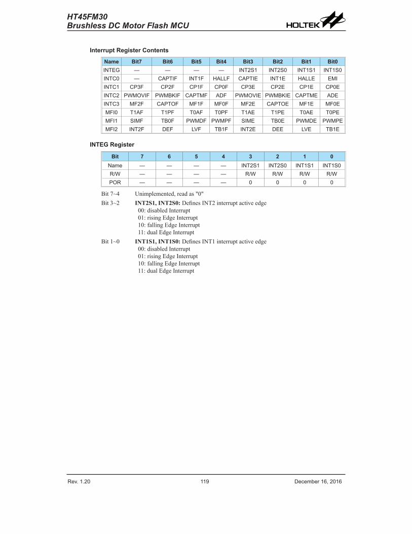
Rev. 1.20 118 De�e��e� 1�� 201� Rev. 1.20 119 De�e��e� 1�� 201�
HT45FM30Brushless DC Motor Flash MCU
Interrupt Register Contents
Name Bit7 Bit6 Bit5 Bit4 Bit3 Bit2 Bit1 Bit0INTEG — — — — INT2S1 INT2S0 INT1S1 INT1S0INTC0 — CAPTIF INT1F HALLF CAPTIE INT1E HALLE EMIINTC1 CP3F CP2F CP1F CP0F CP3E CP2E CP1E CP0EINTC2 PWMOVIF PWMBKIF CAPTMF ADF PWMOVIE PWMBKIE CAPTME ADEINTC3 MF2F CAPTOF MF1F MF0F MF2E CAPTOE MF1E MF0EMFI0 T1AF T1PF T0AF T0PF T1AE T1PE T0AE T0PEMFI1 SIMF TB0F PWMDF PWMPF SIME TB0E PWMDE PWMPEMFI2 INT2F DEF LVF TB1F INT2E DEE LVE TB1E
INTEG Register
Bit 7 6 5 4 3 2 1 0Na�e — — — — INT2S1 INT2S0 INT1S1 INT1S0R/W — — — — R/W R/W R/W R/WPOR — — — — 0 0 0 0
Bit7~4 Unimplemented,readas"0"Bit3~2 INT2S1, INT2S0:DefinesINT2interruptactiveedge
00:disabledInterrupt01:risingEdgeInterrupt10:fallingEdgeInterrupt11:dualEdgeInterrupt
Bit1~0 INT1S1, INT1S0:DefinesINT1interruptactiveedge00:disabledInterrupt01:risingEdgeInterrupt10:fallingEdgeInterrupt11:dualEdgeInterrupt
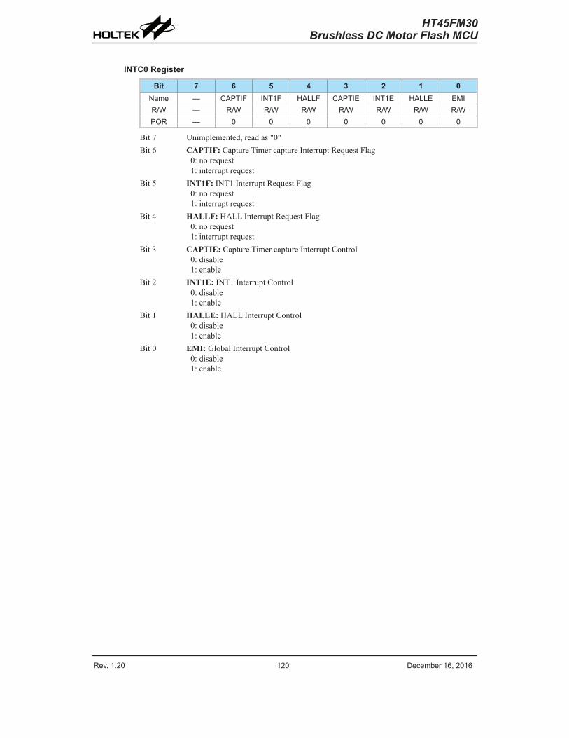
Rev. 1.20 120 De�e��e� 1�� 201� Rev. 1.20 121 De�e��e� 1�� 201�
HT45FM30Brushless DC Motor Flash MCU
INTC0 Register
Bit 7 6 5 4 3 2 1 0Na�e — CAPTIF INT1F HALLF CAPTIE INT1E HALLE EMIR/W — R/W R/W R/W R/W R/W R/W R/WPOR — 0 0 0 0 0 0 0
Bit7 Unimplemented,readas"0"Bit6 CAPTIF:CaptureTimercaptureInterruptRequestFlag
0:norequest1:interruptrequest
Bit5 INT1F:INT1InterruptRequestFlag0:norequest1:interruptrequest
Bit4 HALLF:HALLInterruptRequestFlag0:norequest1:interruptrequest
Bit3 CAPTIE:CaptureTimercaptureInterruptControl0:disable1:enable
Bit2 INT1E:INT1InterruptControl0:disable1:enable
Bit1 HALLE:HALLInterruptControl0:disable1:enable
Bit0 EMI:GlobalInterruptControl0:disable1:enable
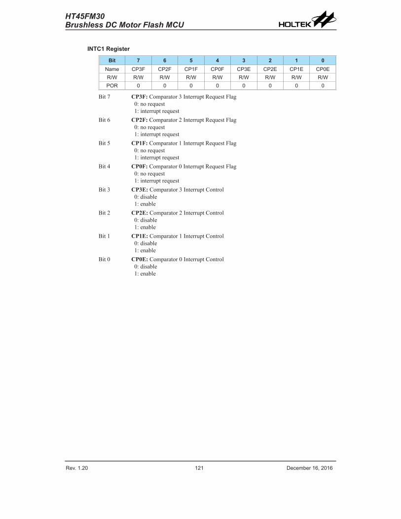
Rev. 1.20 120 De�e��e� 1�� 201� Rev. 1.20 121 De�e��e� 1�� 201�
HT45FM30Brushless DC Motor Flash MCU
INTC1 Register
Bit 7 6 5 4 3 2 1 0Na�e CP3F CP2F CP1F CP0F CP3E CP2E CP1E CP0ER/W R/W R/W R/W R/W R/W R/W R/W R/WPOR 0 0 0 0 0 0 0 0
Bit7 CP3F:Comparator3InterruptRequestFlag0:norequest1:interruptrequest
Bit6 CP2F:Comparator2InterruptRequestFlag0:norequest1:interruptrequest
Bit5 CP1F:Comparator1InterruptRequestFlag0:norequest1:interruptrequest
Bit4 CP0F:Comparator0InterruptRequestFlag0:norequest1:interruptrequest
Bit3 CP3E:Comparator3InterruptControl0:disable1:enable
Bit2 CP2E:Comparator2InterruptControl0:disable1:enable
Bit1 CP1E:Comparator1InterruptControl0:disable1:enable
Bit0 CP0E:Comparator0InterruptControl0:disable1:enable

Rev. 1.20 122 De�e��e� 1�� 201� Rev. 1.20 123 De�e��e� 1�� 201�
HT45FM30Brushless DC Motor Flash MCU
INTC2 Register
Bit 7 6 5 4 3 2 1 0Na�e PWMOVIF PWMBKIF CAPTMF ADF PWMOVIE PWMBKIE CAPTME ADER/W R/W R/W R/W R/W R/W R/W R/W R/WPOR 0 0 0 0 0 0 0 0
Bit7 PWMOVIF:PWMOvercurrentInterruptRequestFlag0:norequest1:interruptrequest
Bit6 PWMBKIF:PWMBrakeInterruptRequestFlag0:norequest1:interruptrequest
Bit5 CAPTMF:CaptureTimerComparematchInterruptRequestFlag0:norequest1:interruptrequest
Bit4 ADF :A/DConverterInterruptRequestFlag0:norequest1:interruptrequest
Bit3 PWMOVIE:PWMOvercurrentInterruptControl0:disable1:enable
Bit2 PWMBKIE:PWMBrakeInterruptControl0:disable1:enable
Bit1 CAPTME:CaptureTimerComparematchInterruptControl0:disable1:enable
Bit0 ADE:A/DConverterInterruptControl0:disable1:enable
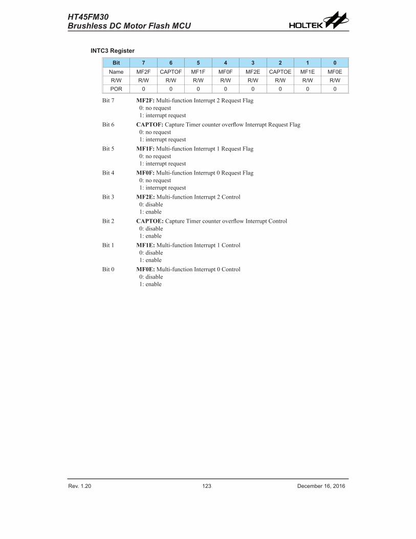
Rev. 1.20 122 De�e��e� 1�� 201� Rev. 1.20 123 De�e��e� 1�� 201�
HT45FM30Brushless DC Motor Flash MCU
INTC3 Register
Bit 7 6 5 4 3 2 1 0Na�e MF2F CAPTOF MF1F MF0F MF2E CAPTOE MF1E MF0ER/W R/W R/W R/W R/W R/W R/W R/W R/WPOR 0 0 0 0 0 0 0 0
Bit7 MF2F:Multi-functionInterrupt2RequestFlag0:norequest1:interruptrequest
Bit6 CAPTOF:CaptureTimercounteroverflowInterruptRequestFlag0:norequest1:interruptrequest
Bit5 MF1F:Multi-functionInterrupt1RequestFlag0:norequest1:interruptrequest
Bit4 MF0F:Multi-functionInterrupt0RequestFlag0:norequest1:interruptrequest
Bit3 MF2E:Multi-functionInterrupt2Control0:disable1:enable
Bit2 CAPTOE:CaptureTimercounteroverflowInterruptControl0:disable1:enable
Bit1 MF1E:Multi-functionInterrupt1Control0:disable1:enable
Bit0 MF0E:Multi-functionInterrupt0Control0:disable1:enable
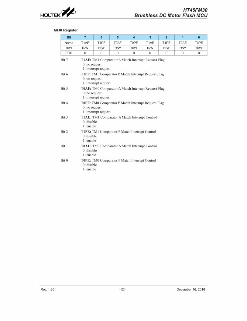
Rev. 1.20 124 De�e��e� 1�� 201� Rev. 1.20 125 De�e��e� 1�� 201�
HT45FM30Brushless DC Motor Flash MCU
MFI0 Register
Bit 7 6 5 4 3 2 1 0Na�e T1AF T1PF T0AF T0PF T1AE T1PE T0AE T0PER/W R/W R/W R/W R/W R/W R/W R/W R/WPOR 0 0 0 0 0 0 0 0
Bit7 T1AF:TM1ComparatorAMatchInterruptRequestFlag0:norequest1:interruptrequest
Bit6 T1PF:TM1ComparatorPMatchInterruptRequestFlag0:norequest1:interruptrequest
Bit5 T0AF:TM0ComparatorAMatchInterruptRequestFlag0:norequest1:interruptrequest
Bit4 T0PF:TM0ComparatorPMatchInterruptRequestFlag0:norequest1:interruptrequest
Bit3 T1AE:TM1ComparatorAMatchInterruptControl0:disable1:enable
Bit2 T1PE:TM1ComparatorPMatchInterruptControl0:disable1:enable
Bit1 T0AE:TM0ComparatorAMatchInterruptControl0:disable1:enable
Bit0 T0PE:TM0ComparatorPMatchInterruptControl0:disable1:enable
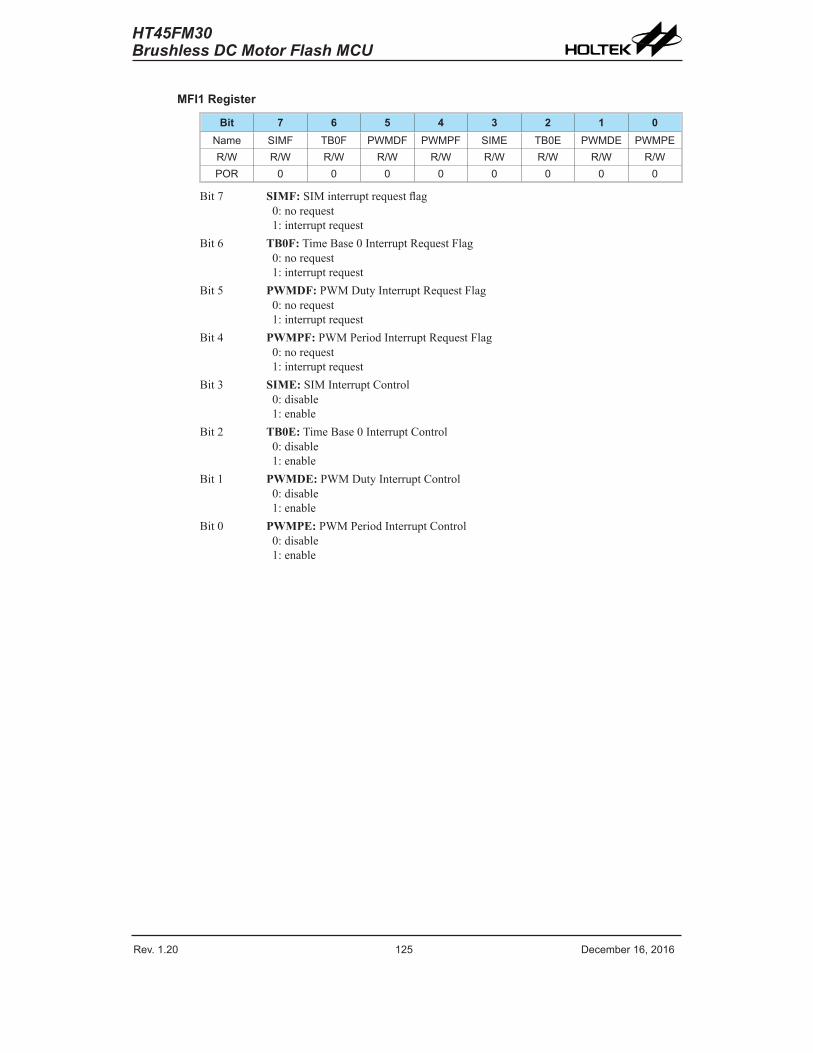
Rev. 1.20 124 De�e��e� 1�� 201� Rev. 1.20 125 De�e��e� 1�� 201�
HT45FM30Brushless DC Motor Flash MCU
MFI1 Register
Bit 7 6 5 4 3 2 1 0Na�e SIMF TB0F PWMDF PWMPF SIME TB0E PWMDE PWMPER/W R/W R/W R/W R/W R/W R/W R/W R/WPOR 0 0 0 0 0 0 0 0
Bit7 SIMF:SIMinterruptrequestflag0:norequest1:interruptrequest
Bit6 TB0F:TimeBase0InterruptRequestFlag0:norequest1:interruptrequest
Bit5 PWMDF:PWMDutyInterruptRequestFlag0:norequest1:interruptrequest
Bit4 PWMPF:PWMPeriodInterruptRequestFlag0:norequest1:interruptrequest
Bit3 SIME:SIMInterruptControl0:disable1:enable
Bit2 TB0E:TimeBase0InterruptControl0:disable1:enable
Bit1 PWMDE:PWMDutyInterruptControl0:disable1:enable
Bit0 PWMPE:PWMPeriodInterruptControl0:disable1:enable
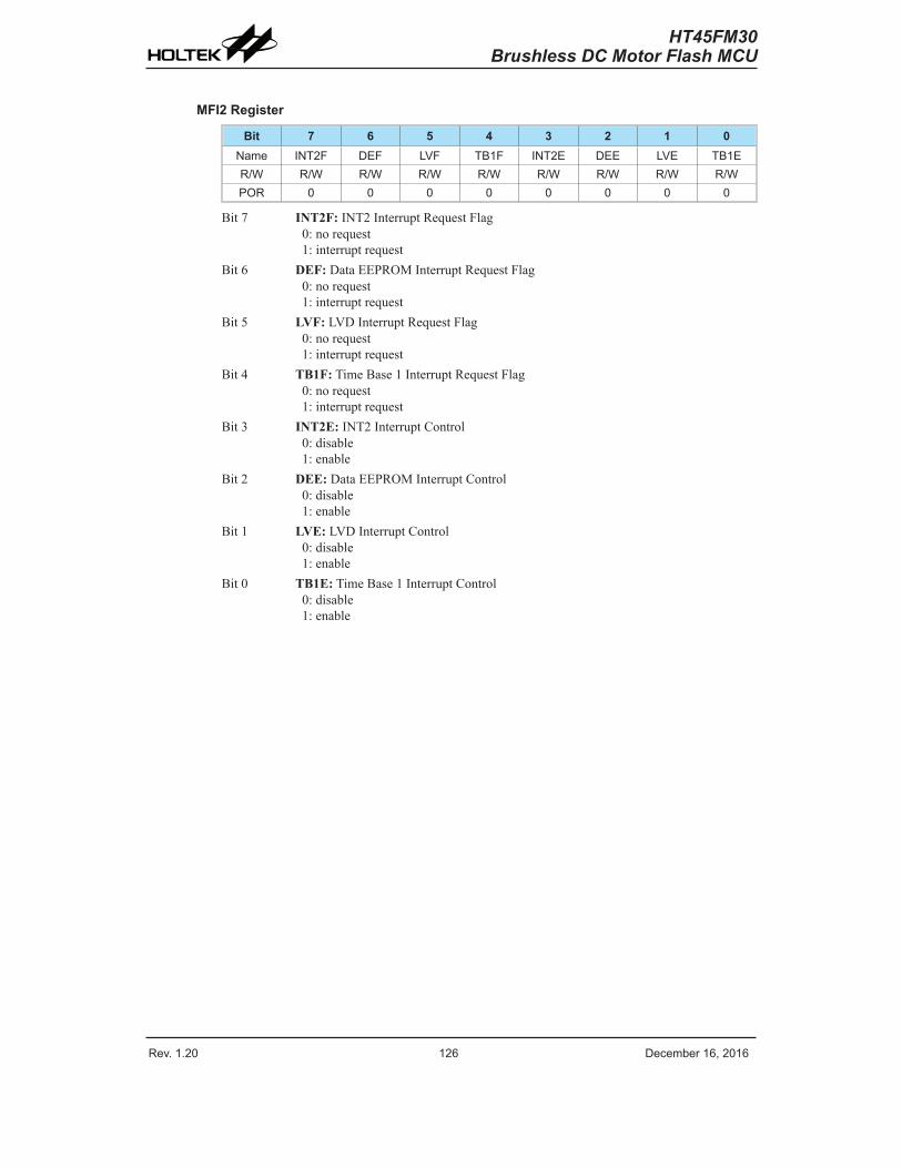
Rev. 1.20 12� De�e��e� 1�� 201� Rev. 1.20 127 De�e��e� 1�� 201�
HT45FM30Brushless DC Motor Flash MCU
MFI2 Register
Bit 7 6 5 4 3 2 1 0Na�e INT2F DEF LVF TB1F INT2E DEE LVE TB1ER/W R/W R/W R/W R/W R/W R/W R/W R/WPOR 0 0 0 0 0 0 0 0
Bit7 INT2F:INT2InterruptRequestFlag0:norequest1:interruptrequest
Bit6 DEF:DataEEPROMInterruptRequestFlag0:norequest1:interruptrequest
Bit5 LVF:LVDInterruptRequestFlag0:norequest1:interruptrequest
Bit4 TB1F:TimeBase1InterruptRequestFlag0:norequest1:interruptrequest
Bit3 INT2E:INT2InterruptControl0:disable1:enable
Bit2 DEE:DataEEPROMInterruptControl0:disable1:enable
Bit1 LVE:LVDInterruptControl0:disable1:enable
Bit0 TB1E:TimeBase1InterruptControl0:disable1:enable
Rev. 1.20 12� De�e��e� 1�� 201� Rev. 1.20 127 De�e��e� 1�� 201�
HT45FM30Brushless DC Motor Flash MCU
Interrupt OperationWhentheconditionsforaninterrupteventoccur,suchasaTMComparatorP,ComparatorAmatchorA/Dconversioncompletionetc,therelevantinterruptrequestflagwillbeset.Whethertherequestflagactuallygeneratesaprogramjumptotherelevantinterruptvectorisdeterminedbytheconditionoftheinterruptenablebit.If theenablebit issethighthentheprogramwill jumptoitsrelevantvector;iftheenablebitiszerothenalthoughtheinterruptrequestflagissetanactualinterruptwillnotbegeneratedandtheprogramwillnotjumptotherelevantinterruptvector.Theglobalinterruptenablebit,ifclearedtozero,willdisableallinterrupts.
Whenaninterruptisgenerated,theProgramCounter,whichstorestheaddressofthenextinstructiontobeexecuted,willbetransferredontothestack.TheProgramCounterwillthenbeloadedwithanewaddresswhichwillbethevalueofthecorrespondinginterruptvector.Themicrocontrollerwillthenfetchitsnextinstructionfromthisinterruptvector.Theinstructionatthisvectorwillusuallybea“JMP”whichwilljumptoanothersectionofprogramwhichisknownastheinterruptserviceroutine.
Hereislocatedthecodetocontroltheappropriateinterrupt.Theinterruptserviceroutinemustbeterminatedwitha“RETI”,whichretrieves theoriginalProgramCounteraddressfromthestackandallowsthemicrocontrollertocontinuewithnormalexecutionat thepointwheretheinterruptoccurred.
Someinterruptsourceshavetheirownindividualvectorwhileotherssharethesamemulti-functioninterruptvector.Onceaninterruptsubroutineisserviced,alltheotherinterruptswillbeblocked,astheglobalinterruptenablebit,EMIbitwillbeclearedautomatically.Thiswillpreventanyfurtherinterruptnestingfromoccurring.However, ifother interruptrequestsoccurduring this interval,althoughtheinterruptwillnotbeimmediatelyserviced,therequestflagwillstillberecorded.
Ifaninterruptrequiresimmediateservicingwhiletheprogramisalreadyinanotherinterruptserviceroutine,theEMIbitshouldbesetafterenteringtheroutine,toallowinterruptnesting.Ifthestackisfull,theinterruptrequestwillnotbeacknowledged,eveniftherelatedinterruptisenabled,untiltheStackPointerisdecremented.Ifimmediateserviceisdesired,thestackmustbepreventedfrombecomingfull.
Alloftheinterruptrequestflagswhensetwillwake-upthedeviceifitisinSLEEPorIDLEMode,howevertopreventawake-upfromoccurringthecorrespondingflagshouldbesetbeforethedeviceisinSLEEPorIDLEMode.
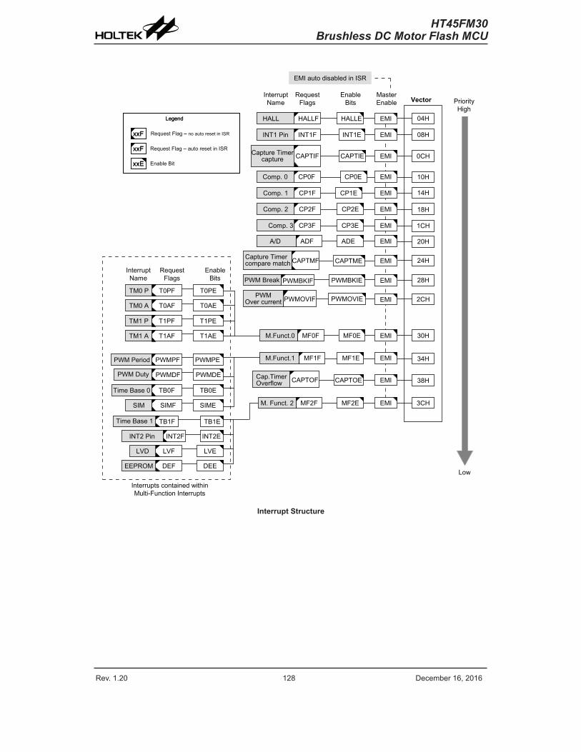
Rev. 1.20 128 De�e��e� 1�� 201� Rev. 1.20 129 De�e��e� 1�� 201�
HT45FM30Brushless DC Motor Flash MCU
04H
08H
14H
18H
1CH
20H
2CH
24H
34H
38H
RequestFlags
EnableBits
EMI auto disabled in ISR
Interrupts contained withinMulti-Function Interrupts
InterruptName
xxF
Legend
Request Flag – no auto reset in ISR
xxF Request Flag – auto reset in ISR
xxE Enable Bit
xxF
Legend
–
xxF
xxE
PWMBKIFPWM Break PWMBKIE
INT2FINT2 Pin INT2E
EMI 28H
LVFLVD LVE
DEFEEPROM DEE
EMI
EMI
EMI
EMI
EMI
EMI
EMI
EMI
EMI
TB1FTime Base 1 TB1E
T1AFTM1 A T1AE
T1PFTM1 P T1PE
T0AFTM0 A T0AE
T0PFTM0 P T0PE
HALLFHALL HALLE
INT1FINT1 Pin INT1E
CP1FComp. 1 CP1E
CP2FComp. 2 CP2E
CP3FComp. 3 CP3E
ADFA/D ADE
PWMOVIFPWMOver current PWMOVIE EMI
CAPTMFCapture Timercompare match CAPTME
MF1FM.Funct.1 MF1E
CAPTOFCap.TimerOverflow CAPTOE
SIMFSIM SIME
TB0FTime Base 0 TB0E
EMI
EMICAPTIFCapture Timercapture CAPTIE
CP0FComp. 0 CP0E
0CH
10H
MF2FM. Funct. 2 MF2E EMI 3CH
30HEMIMF0FM.Funct.0 MF0E
PWMDFPWM Duty PWMDE
PWMPFPWM Period
Low
PriorityHigh
VectorRequest
FlagsEnable
BitsMasterEnable
InterruptName
PWMPE
Interrupt Structure
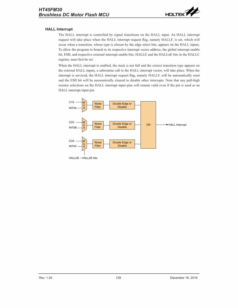
Rev. 1.20 128 De�e��e� 1�� 201� Rev. 1.20 129 De�e��e� 1�� 201�
HT45FM30Brushless DC Motor Flash MCU
HALL InterruptTheHALLinterrupt iscontrolledbysignal transitionson theHALLinput.AnHALLinterruptrequestwill takeplacewhentheHALLinterruptrequestflag,namelyHALLF,isset,whichwilloccurwhenatransition,whosetypeischosenbytheedgeselectbits,appearsontheHALLinputs.Toallowtheprogramtobranchtoitsrespectiveinterruptvectoraddress,theglobalinterruptenablebit,EMI,andrespectiveexternalinterruptenablebits,HALLEandtheHALLnEbitsintheHALLCregister,mustfirstbeset.
WhentheHALLinterruptisenabled,thestackisnotfullandthecorrecttransitiontypeappearsontheexternalHALLinputs,asubroutinecalltotheHALLinterruptvector,willtakeplace.Whentheinterruptisserviced,theHALLinterruptrequestflag,namelyHALLF,willbeautomaticallyresetandtheEMIbitwillbeautomaticallyclearedtodisableother interrupts.Notethatanypull-highresistorselectionsontheHALLinterruptinputpinswillremainvalidevenifthepinisusedasanHALLinterruptinputpin.
MUX
MUX
MUX
NoiseFilter
Double Edge orDisable
Double Edge orDisable
Double Edge orDisable
NoiseFilter
C1X
C2X
C3X
INT0A
INT0B
INT0C
HALL0E ~ HALL2E bits
OR HALL Interrupt
NoiseFilter
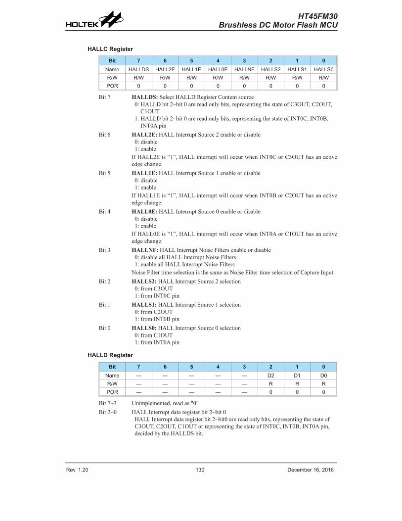
Rev. 1.20 130 De�e��e� 1�� 201� Rev. 1.20 131 De�e��e� 1�� 201�
HT45FM30Brushless DC Motor Flash MCU
HALLC Register
Bit 7 6 5 4 3 2 1 0Na�e HALLDS HALL2E HALL1E HALL0E HALLNF HALLS2 HALLS1 HALLS0R/W R/W R/W R/W R/W R/W R/W R/W R/WPOR 0 0 0 0 0 0 0 0
Bit7 HALLDS:SelectHALLDRegisterContentsource0:HALLDbit2~bit0arereadonlybits,representingthestateofC3OUT,C2OUT,C1OUT1:HALLDbit2~bit0arereadonlybits,representingthestateofINT0C,INT0B,INT0Apin
Bit6 HALL2E:HALLInterruptSource2enableordisable0:disable1:enableIfHALL2Eis“1”,HALLinterruptwilloccurwhenINT0CorC3OUThasanactiveedgechange.
Bit5 HALL1E:HALLInterruptSource1enableordisable0:disable1:enableIfHALL1Eis“1”,HALLinterruptwilloccurwhenINT0BorC2OUThasanactiveedgechange.
Bit4 HALL0E:HALLInterruptSource0enableordisable0:disable1:enableIfHALL0Eis“1”,HALLinterruptwilloccurwhenINT0AorC1OUThasanactiveedgechange.
Bit3 HALLNF:HALLInterruptNoiseFiltersenableordisable0:disableallHALLInterruptNoiseFilters1:enableallHALLInterruptNoiseFiltersNoiseFiltertimeselectionisthesameasNoiseFiltertimeselectionofCaptureInput.
Bit2 HALLS2:HALLInterruptSource2selection0:fromC3OUT1:fromINT0Cpin
Bit1 HALLS1:HALLInterruptSource1selection0:fromC2OUT1:fromINT0Bpin
Bit0 HALLS0:HALLInterruptSource0selection0:fromC1OUT1:fromINT0Apin
HALLD Register
Bit 7 6 5 4 3 2 1 0Na�e — — — — — D2 D1 D0R/W — — — — — R R RPOR — — — — — 0 0 0
Bit7~3 Unimplemented,readas"0"Bit2~0 HALLInterruptdataregisterbit2~bit0
HALLInterruptdataregisterbit2~bit0arereadonlybits,representingthestateofC3OUT,C2OUT,C1OUTorrepresentingthestateofINT0C,INT0B,INT0Apin,decidedbytheHALLDSbit.
Rev. 1.20 130 De�e��e� 1�� 201� Rev. 1.20 131 De�e��e� 1�� 201�
HT45FM30Brushless DC Motor Flash MCU
External Interrupt Theexternal interruptsarecontrolledbysignal transitionson thepinsINT1,INT2.Anexternalinterruptrequestwill takeplacewhentheexternal interruptrequestflags,INT1F,INT2F,areset,whichwilloccurwhenatransition,whosetypeischosenbytheedgeselectbits,appearsontheexternalinterruptpins.Toallowtheprogramtobranchtoitsrespectiveinterruptvectoraddress,theglobalinterruptenablebit,EMI,andrespectiveexternalinterruptenablebit,INT1E,INT2E,mustfirstbeset.NotethatduetotheINT2islocatedinMulti-functionInterrupt2,therefore,theMF2EmustalsobesettoenabletheINT2interruptfunction.AdditionallythecorrectinterruptedgetypemustbeselectedusingtheINTEGregistertoenabletheexternalinterruptfunctionandtochoosethe triggeredge type.As theexternal interruptpinsarepin-sharedwithI/Opins, theycanonlybeconfiguredasexternal interruptpinsif theirexternal interruptenablebit in thecorrespondinginterruptregisterhasbeenset.
Thepinmustalsobesetupasaninputbysettingthecorrespondingbitintheportcontrolregister.Whentheinterrupt isenabled, thestackisnotfullandthecorrect transitiontypeappearsontheexternalinterruptpin,asubroutinecall totheexternalinterruptvector,will takeplace.Whentheinterrupt isserviced, theexternal interrupt1requestflag,INT1F,willbeautomaticallyresetandtheEMIbitwillbeautomaticallyclearedtodisableotherinterrupts.NotethatduetotheINT2islocatedinMulti-functioninterrupt,therefore,theINT2Fwillnotbeautomaticallyresetandmustbemanuallyresetbytheapplicationprogram.Anypull-highresistorselectionsontheexternalinterruptpinswillremainvalidevenifthepinisusedasanexternalinterruptinput.
TheINTEGregisterisusedtoselectthetypeofactiveedgethatwilltriggertheexternalinterrupt.Achoiceofeitherrisingorfallingorbothedgetypescanbechosentotriggeranexternalinterrupt.NotethattheINTEGregistercanalsobeusedtodisabletheexternalinterruptfunction.
Capture Timer Module InterruptTheCaptureTimerModulehas three interrupts, includingCapture Interrupt,ComparematchinterruptandCapturecounteroverflowinterrupt.ThesethreeInterruptsrequestwilltakeplacewhentheCaptureTimerModulerequestflags,CAPTIF,CAPTMF,andCAPTOFareset.Toallowtheprogramtobranchtoitsrespectiveinterruptvectoraddress, theglobal interruptenablebit,EMI,andrespectiveCaptureTimerModuleInterruptenablebit,mustfirstbeset.Whentheinterruptisenabled,thestackisnotfullandthecaptureblocks,ComparematchorCapturecounteroverflowaretriggered,asubroutinecall totherelevantinterruptvectorlocation,will takeplace.WhentheCaptureTimerModuleinterruptisserviced,thecorrespondingrequestflagswillbeautomaticallyresetandtheEMIbitwillbeautomaticallyclearedtodisableotherinterrupts.
Rev. 1.20 132 De�e��e� 1�� 201� Rev. 1.20 133 De�e��e� 1�� 201�
HT45FM30Brushless DC Motor Flash MCU
Comparator InterruptThecomparator interrupt iscontrolledbythefour internalcomparators.Acomparator interruptrequestwilltakeplacewhenthecomparatorinterruptrequestflags,CP0F~CP3F,areset,asituationthatwilloccurwhenthecomparatoroutputchangesstate.Toallowtheprogramtobranchtoitsrespectiveinterruptvectoraddress, theglobalinterruptenablebit,EMI,andcomparatorinterruptenablebits,CP0E~CP3E,mustfirstbeset.Whentheinterruptisenabled,thestackisnotfullandthecomparatorinputsgenerateacomparatoroutputtransition,asubroutinecall tothecomparatorinterruptvector,willtakeplace.Whentheinterruptisserviced,thecorrespondingrequestflagswillbeautomaticallyresetandtheEMIbitwillbeautomaticallyclearedtodisableotherinterrupts.
A/D Converter InterruptThisdevicecontainsanA/Dconverterwhichhasitsownindependentinterrupt.TheA/DConverterInterruptiscontrolledbytheterminationofanA/Dconversionprocess.AnA/DConverterInterruptrequestwill takeplacewhentheA/DConverterInterruptrequestflag,ADF, isset,whichoccurswhentheA/Dconversionprocessfinishes.Toallowtheprogramtobranchtoitsrespectiveinterruptvectoraddress,theglobalinterruptenablebit,EMI,andA/DInterruptenablebit,ADE,mustfirstbeset.Whentheinterruptisenabled,thestackisnotfullandtheA/Dconversionprocesshasended,asubroutinecalltotheA/DConverterInterruptvector,willtakeplace.Whentheinterruptisserviced,theA/DConverterInterruptflag,ADF,willbeautomaticallycleared.TheEMIbitwillalsobeautomaticallyclearedtodisableotherinterrupts.
PWM Automatic Brake Control InterruptThePWMAutomaticBrakeControlhasaninterrupt,PWMBrakeInterrupt.Thereisoneinterruptrequest flagPWMBKIFandoneenablebitPWMBKIE.APWMBrake interrupt requestwilltakeplacewhenthePWMBrakerequestflagisset,asituationwhichoccurswhenaPWMBrakesituationhappens.Toallowtheprogramtobranchto its respective interruptvectoraddress, theglobal interruptenablebit,EMI, respectivePWMBreakInterruptenablebitmust firstbeset.Whentheinterruptisenabled,thestackisnotfullandaPWMBreaksituationoccurs,asubroutinecall totherelevantInterruptvectorlocations,will takeplace.Whentheinterruptisserviced, thePWMBrakeInterrupt flag,PWMBKIF,willbeautomaticallycleared.TheEMIbitwillalsobeautomaticallyclearedtodisableotherinterrupts.
Over current Protection InterruptThePWMOverCurrentProtectionhasaninterrupt,PWMOverCurrentInterrupt.There isoneinterruptrequestflagPWMOVIFandoneenablebitPWMOVIE.APWMOverCurrentrequestwilltakeplacewhenthePWMOverCurrentrequestflagisset,asituationwhichoccurswhenaPWMOverCurrentsituationhappens.Toallowtheprogramtobranchtoitsrespectiveinterruptvectoraddress,theglobalinterruptenablebit,EMI,respectivePWMOverCurrentenablebitmustfirstbeset.Whentheinterruptisenabled,thestackisnotfullandaPWMOverCurrentoccurs,asubroutinecall totherelevantInterruptvectorlocations,will takeplace.Whentheinterruptisserviced, thePWMOverCurrentInterruptflag,PWMOVIF,willbeautomaticallycleared.TheEMIbitwillalsobeautomaticallyclearedtodisableotherinterrupts.
Rev. 1.20 132 De�e��e� 1�� 201� Rev. 1.20 133 De�e��e� 1�� 201�
HT45FM30Brushless DC Motor Flash MCU
Multi-function InterruptsWithinthedevicetherearesomeMulti-functioninterrupts.Unliketheotherindependentinterrupts,these interruptshavenoindependentsource,butratherareformedfromotherexistinginterruptsources,namely theTMInterrupts,PWMPeriod Interrupt,PWMDuty Interrupt,TimeBaseinterrupts,SIMinterrupt,LVDinterrupt,EEPROMinterruptandExternalInterrupt2interrupt.
AMulti-functioninterruptrequestwilltakeplacewhenanyoftheMulti-functionInterruptrequestflags,MF0F~MF2Fareset.TheMulti-functioninterruptflagswillbesetwhenanyoftheirincludedfunctionsgeneratean interrupt request flag.Toallow theprogram tobranch to its respectiveinterruptvectoraddress,whentheMulti-functioninterruptisenabledandthestackisnotfull,andeitheroneoftheinterruptscontainedwithineachofMulti-functioninterruptoccurs,asubroutinecalltooneoftheMulti-functioninterruptvectorswilltakeplace.Whentheinterruptisserviced,therelatedMulti-FunctionrequestflagwillbeautomaticallyresetandtheEMIbitwillbeautomaticallyclearedtodisableotherinterrupts.
However, itmustbenotedthat,althoughtheMulti-functionInterruptflagswillbeautomaticallyresetwhentheinterruptisserviced,therequestflagsfromtheoriginalsourceoftheMulti-functioninterrupts,namely theTMInterrupts,PWMPeriodInterrupt,PWMDutyInterrupt,TimeBaseinterrupts,SIMinterrupt,LVDinterrupt,EEPROMinterruptandExternalInterrupt2interrupt,willnotbeautomaticallyresetandmustbemanuallyresetbytheapplicationprogram.
TM InterruptsTheCompactandStandardTypeTMshave two interruptseach.Allof theTMinterruptsarecontainedwithintheMulti-functionInterrupts.ForeachoftheCompactandStandardTypeTMstherearetwointerruptrequestflagsTnPFandTnAFandtwoenablebitsTnPEandTnAE.ATMinterruptrequestwilltakeplacewhenanyoftheTMrequestflagsareset,asituationwhichoccurswhenaTMcomparatorPorAmatchsituationhappens.Toallowtheprogramtobranch to itsrespectiveinterruptvectoraddress, theglobal interruptenablebit,EMI,respectiveTMInterruptenablebit,andrelevantMulti-functionInterruptenablebit,MF0E,must firstbeset.Whentheinterruptisenabled,thestackisnotfullandaTMcomparatormatchsituationoccurs,asubroutinecalltotherelevantMulti-functionInterruptvectorlocation,willtakeplace.WhentheTMinterruptisserviced, theEMIbitwillbeautomaticallycleared todisableother interrupts,howeveronlytherelatedMF0Fflagwillbeautomaticallycleared.AstheTMinterruptrequestflagswillnotbeautomaticallycleared,theyhavetobeclearedbytheapplicationprogram.
PWM InterruptThePWMhastwointerruptswhicharecontainedwithintheMulti-functionInterrupts.Therearetwointerruptrequestflags,PWMDFandPWMPF,andtwoenablebits,PWMDEandPWMPE.APWMinterruptrequestwilltakeplacewhenanyofthePWMrequestflagsareset,asituationwhichoccurswhenaPWMcomparatorPeriodorDutymatchsituationhappens.Toallowtheprogramtobranchtoitsrespectiveinterruptvectoraddress,theglobalinterruptenablebit,EMI,respectivePWMInterruptenablebit,andrelevantMulti-functionInterruptenablebit,MF1E,mustfirstbeset.Whentheinterruptisenabled,thestackisnotfullandaPWMcomparatormatchsituationoccurs,asubroutinecall to therelevantMulti-functionInterruptvector locations,will takeplace.WhenthePWMinterruptisserviced,theEMIbitwillbeautomaticallyclearedtodisableotherinterrupts,howeveronlytherelatedMF1Fflagwillbeautomaticallycleared.AsthePWMinterruptrequestflagswillnotbeautomaticallycleared,theyhavetobeclearedbytheapplicationprogram.
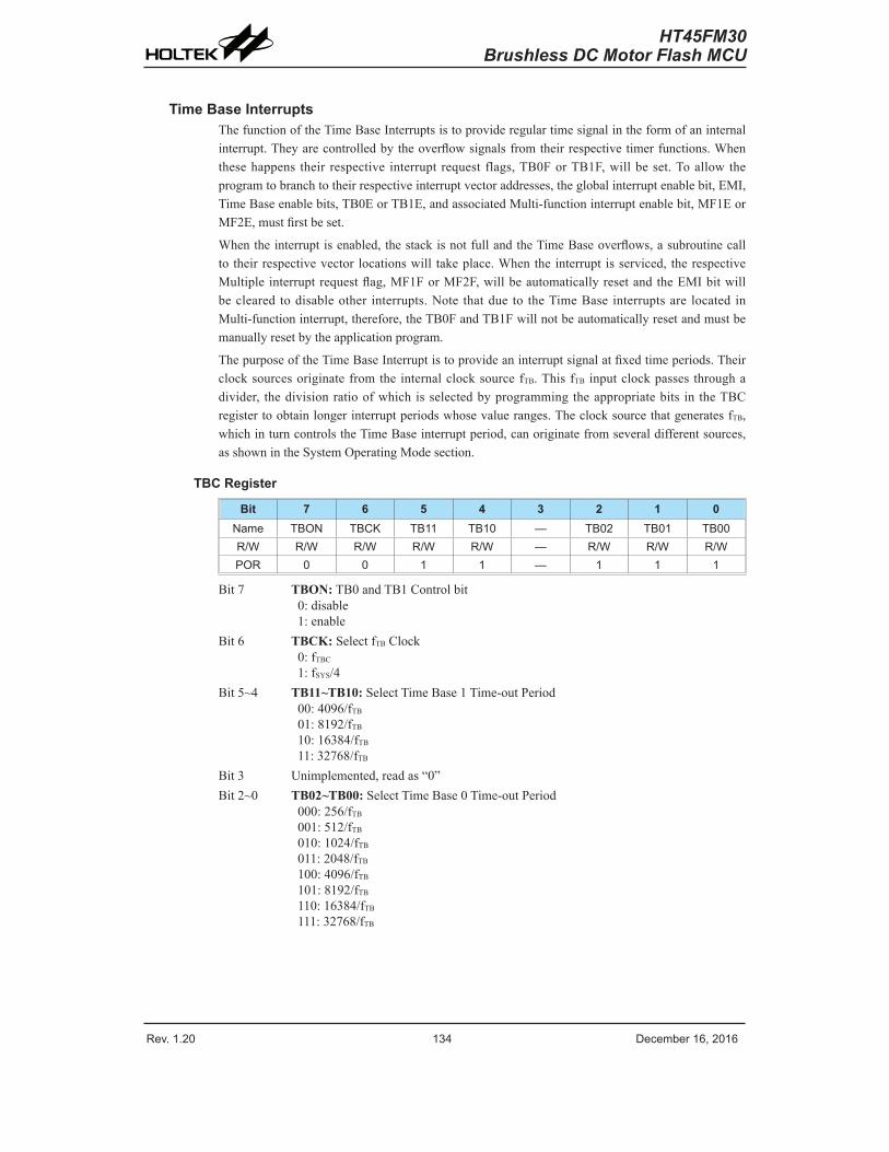
Rev. 1.20 134 De�e��e� 1�� 201� Rev. 1.20 135 De�e��e� 1�� 201�
HT45FM30Brushless DC Motor Flash MCU
Time Base InterruptsThefunctionoftheTimeBaseInterruptsistoprovideregulartimesignalintheformofaninternalinterrupt.Theyarecontrolledbytheoverflowsignalsfromtheirrespectivetimerfunctions.Whenthesehappens their respective interrupt request flags,TB0ForTB1F,willbeset.Toallowtheprogramtobranchtotheirrespectiveinterruptvectoraddresses,theglobalinterruptenablebit,EMI,TimeBaseenablebits,TB0EorTB1E,andassociatedMulti-functioninterruptenablebit,MF1EorMF2E,mustfirstbeset.
Whentheinterruptisenabled,thestackisnotfullandtheTimeBaseoverflows,asubroutinecallto theirrespectivevector locationswill takeplace.Whentheinterrupt isserviced, therespectiveMultiple interruptrequestflag,MF1ForMF2F,willbeautomaticallyresetandtheEMIbitwillbecleared todisableother interrupts.Note thatdue to theTimeBase interruptsare located inMulti-functioninterrupt,therefore,theTB0FandTB1Fwillnotbeautomaticallyresetandmustbemanuallyresetbytheapplicationprogram.
ThepurposeoftheTimeBaseInterruptistoprovideaninterruptsignalatfixedtimeperiods.TheirclocksourcesoriginatefromtheinternalclocksourcefTB.ThisfTB inputclockpasses throughadivider, thedivisionratioofwhich isselectedbyprogrammingtheappropriatebits in theTBCregistertoobtainlongerinterruptperiodswhosevalueranges.TheclocksourcethatgeneratesfTB,whichinturncontrolstheTimeBaseinterruptperiod,canoriginatefromseveraldifferentsources,asshownintheSystemOperatingModesection.
TBC Register
Bit 7 6 5 4 3 2 1 0Na�e TBON TBCK TB11 TB10 — TB02 TB01 TB00R/W R/W R/W R/W R/W — R/W R/W R/WPOR 0 0 1 1 — 1 1 1
Bit7 TBON:TB0andTB1Controlbit0:disable1:enable
Bit6 TBCK:SelectfTBClock0:fTBC1:fSYS/4
Bit5~4 TB11~TB10:SelectTimeBase1Time-outPeriod00:4096/fTB01:8192/fTB10:16384/fTB11:32768/fTB
Bit3 Unimplemented,readas“0”Bit2~0 TB02~TB00:SelectTimeBase0Time-outPeriod
000:256/fTB001:512/fTB010:1024/fTB011:2048/fTB100:4096/fTB101:8192/fTB110:16384/fTB111:32768/fTB
Rev. 1.20 134 De�e��e� 1�� 201� Rev. 1.20 135 De�e��e� 1�� 201�
HT45FM30Brushless DC Motor Flash MCU
���� � � �
� � � � � �� � � � � � �� � �
� � � � � � � �� � � �
� � � � � � �
� � � � � � � � � � � � � � � � � �
� � � � � � � � � � � � � � � � � �
� � � � � �
� � � � � � �
� �� � �
Time Base Interrupt
• SerialInterfaceModuleInterruptTheSerialInterfaceModuleInterrupt,alsoknownastheSIMinterrupt, iscontainedwithintheMulti-functionInterrupt.ASIMInterruptrequestwilltakeplacewhentheSIMInterruptrequestflag,SIMF,isset,whichoccurswhenabyteofdatahasbeenreceivedortransmittedbytheSIMinterface.Toallowtheprogramtobranchto itsrespective interruptvectoraddress, theglobalinterruptenablebit,EMI,andtheSerialInterfaceInterruptenablebit,SIME,andtherespectiveMulti-functioninterruptenablebit,mustfirstbeset.Whentheinterruptisenabled,thestackisnotfullandabyteofdatahasbeentransmittedorreceivedbytheSIMinterface,asubroutinecalltotherespectiveMulti-functionInterruptvector,willtakeplace.WhentheSerialInterfaceInterruptisserviced,theEMIbitwillbeautomaticallyclearedtodisableotherinterrupts,howeveronlytheMulti-functioninterruptrequestflagwillbealsoautomaticallycleared.AstheSIMFflagwillnotbeautomaticallycleared,ithastobeclearedbytheapplicationprogram.
LVD InterruptTheLowVoltageDetector Interrupt iscontainedwithin theMulti-function Interrupt.AnLVDInterruptrequestwill takeplacewhentheLVDInterruptrequest flag,LVF, isset,whichoccurswhentheLowVoltageDetectorfunctiondetectsalowpowersupplyvoltage.Toallowtheprogramtobranchtoitsrespectiveinterruptvectoraddress,theglobalinterruptenablebit,EMI,LowVoltageInterruptenablebit,LVE,andassociatedMulti-functioninterruptenablebit,mustfirstbeset.Whentheinterruptisenabled,thestackisnotfullandalowvoltageconditionoccurs,asubroutinecalltotheMulti-functionInterruptvector,willtakeplace.WhentheLowVoltageInterruptisserviced,theEMIbitwillbeautomaticallyclearedtodisableotherinterrupts,howeveronlytheMulti-functioninterruptrequestflagwillbealsoautomaticallycleared.AstheLVFflagwillnotbeautomaticallycleared,ithastobeclearedbytheapplicationprogram.
Rev. 1.20 13� De�e��e� 1�� 201� Rev. 1.20 137 De�e��e� 1�� 201�
HT45FM30Brushless DC Motor Flash MCU
EEPROM InterruptTheEEPROMinterrupt, iscontainedwithintheMulti-functionInterrupt.AnEEPROMInterruptrequestwill takeplacewhentheEEPROMInterruptrequestflag,DEF,isset,whichoccurswhenanEEPROMWritecycleends.Toallowtheprogramtobranchtoitsrespectiveinterruptvectoraddress, theglobalinterruptenablebit,EMI,EEPROMInterruptenablebit,DEE,andassociatedMulti-functioninterruptenablebit,mustfirstbeset.Whentheinterruptisenabled,thestackisnotfullandanEEPROMWritecycleends,asubroutinecalltotherespectiveMulti-functionInterruptvector,willtakeplace.WhentheEEPROMInterruptisserviced,theEMIbitwillbeautomaticallyclearedtodisableotherinterrupts,howeveronlytheMulti-functioninterruptrequestflagwillbealsoautomaticallycleared.AstheDEFflagwillnotbeautomaticallycleared,ithastobeclearedbytheapplicationprogram.
Interrupt Wake-up FunctionEachof the interruptfunctionshas thecapabilityofwakingupthemicrocontrollerwhenin theSLEEPorIDLEMode.Awake-upisgeneratedwhenaninterruptrequestflagchangesfromlowtohighandisindependentofwhethertheinterruptisenabledornot.Therefore,eventhoughthedeviceisintheSLEEPorIDLEModeanditssystemoscillatorstopped,situationssuchasexternaledgetransitionsontheexternalinterruptpins,alowpowersupplyvoltageorcomparatorinputchangemaycausetheirrespectiveinterruptflagtobesethighandconsequentlygenerateaninterrupt.Caremust thereforebetakenifspuriouswake-upsituationsaretobeavoided.Ifaninterruptwake-upfunctionistobedisabledthenthecorrespondinginterruptrequestflagshouldbesethighbeforethedeviceenterstheSLEEPorIDLEMode.Theinterruptenablebitshavenoeffectontheinterruptwake-upfunction.
Programming ConsiderationsBydisablingtherelevantinterruptenablebits,arequestedinterruptcanbepreventedfrombeingserviced,however,oncean interrupt request flag is set, itwill remain in thiscondition in theinterruptregisteruntilthecorrespondinginterruptisservicedoruntiltherequestflagisclearedbytheapplicationprogram.Whereacertaininterrupt iscontainedwithinaMulti-functioninterrupt,thenwhentheinterruptserviceroutineisexecuted,asonlytheMulti-functioninterruptrequestflags,MF0F~MF2F,willbeautomaticallycleared,theindividualrequestflagforthefunctionneedstobeclearedbytheapplicationprogram.
It isrecommendedthatprogramsdonotusethe“CALL”instructionwithintheinterruptservicesubroutine.Interruptsoftenoccurinanunpredictablemannerorneedtobeservicedimmediately.Ifonlyonestackisleftandtheinterruptisnotwellcontrolled,theoriginalcontrolsequencewillbedamagedonceaCALLsubroutineisexecutedintheinterruptsubroutine.Everyinterrupthasthecapabilityofwakingupthemicrocontrollerwhenit isinSLEEPorIDLEMode,thewakeupbeinggeneratedwhentheinterruptrequestflagchangesfromlowtohigh.Ifitisrequiredtopreventacertain interruptfromwakingupthemicrocontroller thenitsrespectiverequestflagshouldbefirstsethighbeforeenterSLEEPorIDLEMode.AsonlytheProgramCounterispushedontothestack,thenwhentheinterruptisserviced,ifthecontentsoftheaccumulator,statusregisterorotherregistersarealteredbytheinterruptserviceprogram,theircontentsshouldbesavedtothememoryatthebeginningoftheinterruptserviceroutine.
Toreturnfromaninterruptsubroutine,eitheraRETorRETIinstructionmaybeexecuted.TheRETIinstructioninadditiontoexecutingareturntothemainprogramalsoautomaticallysetstheEMIbithightoallowfurtherinterrupts.TheRETinstructionhoweveronlyexecutesareturntothemainprogramleavingtheEMIbitinitspresentzerostateandthereforedisablingtheexecutionoffurtherinterrupts.
Rev. 1.20 13� De�e��e� 1�� 201� Rev. 1.20 137 De�e��e� 1�� 201�
HT45FM30Brushless DC Motor Flash MCU
Low Voltage Detector – LVDThedevicehasaLowVoltageDetectorfunction,alsoknownasLVD.Thisenabledthedevicetomonitorthepowersupplyvoltage,VDD,andprovideawarningsignalshoulditfallbelowacertainlevel.Thisfunctionmaybeespeciallyusefulinbatteryapplicationswherethesupplyvoltagewillgraduallyreduceasthebatteryages,asitallowsanearlywarningbatterylowsignaltobegenerated.
TheLowVoltageDetectoralsohasthecapabilityofgeneratinganinterruptsignal.
LVD RegisterTheLowVoltageDetectorfunctioniscontrolledusingasingleregisterwiththenameLVDC.Threebitsinthisregister,VLVD2~VLVD0areusedtoselectoneofthreefixedvoltagesbelowwhichalowvoltageconditionwillbedetermined.Alowvoltageconditionis indicatedwhentheLVDObitisset.IftheLVDObitislow,thisindicatesthattheVDDvoltageisabovethepresetlowvoltagevalue.TheLVDENbit isusedtocontrol theoverallon/offfunctionof thelowvoltagedetector.Settingthebithighwillenablethelowvoltagedetector.Clearingthebittozerowillswitchofftheinternallowvoltagedetectorcircuits.Asthelowvoltagedetectorwillconsumeacertainamountofpower,itmaybedesirabletoswitchoffthecircuitwhennotinuse,animportantconsiderationinpowersensitivebatterypoweredapplications.
LVDC Register
Bit 7 6 5 4 3 2 1 0Na�e — — LVDO LVDEN — VLVD2 VLVD1 VLVD0R/W — — R R/W — R/W R/W R/WPOR — — 0 0 — 0 0 0
Bit7~6 Unimplemented,readas"0"Bit5 LVDO:LVDOutputFlag
0:noLowVoltageDetect1:lowVoltageDetect
Bit4 LVDEN:LowVoltageDetectorControl0:disable1:enable
Bit3 Unimplemented,readas"0"Bit2~0 VLVD2~VLVD0:LVDVoltageselectbits
000~100:reserved101:3.3V110:3.6V111:4.2V
Rev. 1.20 138 De�e��e� 1�� 201� Rev. 1.20 139 De�e��e� 1�� 201�
HT45FM30Brushless DC Motor Flash MCU
LVD OperationTheLowVoltageDetectorfunctionoperatesbycomparingthepowersupplyvoltage,VDD,with3.3,3.6or4.2V.Whenthepowersupplyvoltage,VDD,fallsbelowthispre-determinedvalue,theLVDObitwillbesethighindicatinga lowpowersupplyvoltagecondition.TheLowVoltageDetectorfunctionissuppliedbyareferencevoltagewhichwillbeautomaticallyenabled.WhenthedeviceispowereddownthelowvoltagedetectorwillremainactiveiftheLVDENbitishigh.AfterenablingtheLowVoltageDetector,atimedelaytLVDSshouldbeallowedforthecircuitrytostabilisebeforereading theLVDObit.Notealso thatas theVDDvoltagemayriseandfall ratherslowly,at thevoltagenearsthatofVLVD,theremaybemultiplebitLVDOtransitions.
� � �
� � � �
� � � � �
� � � �� � � � �
LVD Operation
TheLowVoltageDetector alsohas its own interruptwhich is containedwithinoneof theMulti-functioninterrupts,providinganalternativemeansof lowvoltagedetection, inadditiontopollingtheLVDObit.TheinterruptwillonlybegeneratedafteradelayoftLVDaftertheLVDObithasbeensethighbyalowvoltagecondition.WhenthedeviceispowereddowntheLowVoltageDetectorwillremainactiveif theLVDENbit ishigh.Inthiscase, theLVFinterruptrequestflagwillbeset,causinganinterrupttobegeneratedifVDDfallsbelowthepresetLVDvoltage.Thiswillcausethedevicetowake-upfromtheSLEEPorIDLEMode,howeveriftheLowVoltageDetectorwakeupfunctionisnotrequiredthentheLVFflagshouldbefirstsethighbeforethedeviceenterstheSLEEPorIDLEMode.
Rev. 1.20 138 De�e��e� 1�� 201� Rev. 1.20 139 De�e��e� 1�� 201�
HT45FM30Brushless DC Motor Flash MCU
Pulse Width ModulatorThisdevice isprovidedwitha three-channel12-bitPWMfunction.EachchannelhasapairofComplementaryPWMoutput.Usefulforsuchapplicationssuchasmotorspeedcontrol,thePWMfunctionprovidesaflexiblesignaloutputwithaselectablefrequencyandwithadutycyclethatcanbevariedbysettingparticular12-bitvaluesintothecorrespondingPWMregisters.TheinclusionofDead-Time insertion,Polaritysettingcontrol,Maskoutputcontrol,PWMPeriodandDutyInterruptsandhighdrivingcurrentabilityensurethatthisdevicewillfindexcellentuseinthe3-PhaseBrushlessDC(BLDC)motorapplicationarea.
PWM Clock SourceThePWMclock,fPWM,issourcedfromthesystemclockfSYS.Itcanbefurthersubdividedusinganinternaldivider toprovideafrequencyrangefromfSYS~fSYS/128usingthePWMCK0~PWMCK2bits in thePWMC1register.Thisclocksource isused todrivean internalPWM12-bitcounterwhichiscomparedwiththeprogrammedPWMdatavalueforperiodanddutycyclecontrol.
ThefollowingdiagramillustratesthebasicoperationofthePWM.
fSYS/1
fPWMMUX
PWMCK[2:0] PWMEN
PWM0H
PWM0L
PWM1H
PWM1L
PWM2H
PWM2L
PWMCENDTEN
PWMGenerator
ComplementaryPWMand
Dead TimeControl
fSYS/2
fSYS/4
fSYS/8
fSYS/16
fSYS/32
fSYS/64
fSYS/128
PnLMENPnHMEN
MaskOutputControl
PnLPPnHP
PolarityControl
PWM Block Diagram
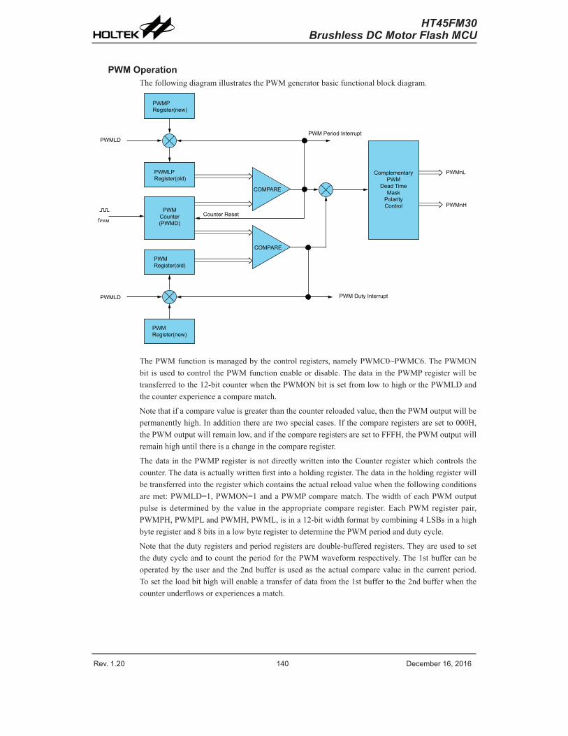
Rev. 1.20 140 De�e��e� 1�� 201� Rev. 1.20 141 De�e��e� 1�� 201�
HT45FM30Brushless DC Motor Flash MCU
PWM OperationThefollowingdiagramillustratesthePWMgeneratorbasicfunctionalblockdiagram.
PWMPRegister(new)
COMPARE
ComplementaryPWM
Dead TimeMask
PolarityControl
COMPARE
PWMLD
PWMnL
PWM Period Interrupt
PWMnH
PWMLPRegister(old)
Counter Reset
PWMRegister(old)
PWMLD PWM Duty Interrupt
PWMRegister(new)
PWMCounter(PWMD)fPWM
ThePWMfunctionismanagedbythecontrolregisters,namelyPWMC0~PWMC6.ThePWMONbitisusedtocontrolthePWMfunctionenableordisable.ThedatainthePWMPregisterwillbetransferredtothe12-bitcounterwhenthePWMONbitissetfromlowtohighorthePWMLDandthecounterexperienceacomparematch.
Notethatifacomparevalueisgreaterthanthecounterreloadedvalue,thenthePWMoutputwillbepermanentlyhigh.Inadditiontherearetwospecialcases.Ifthecompareregistersaresetto000H,thePWMoutputwillremainlow,andifthecompareregistersaresettoFFFH,thePWMoutputwillremainhighuntilthereisachangeinthecompareregister.
ThedatainthePWMPregisterisnotdirectlywrittenintotheCounterregisterwhichcontrolsthecounter.Thedataisactuallywrittenfirstintoaholdingregister.Thedataintheholdingregisterwillbetransferredintotheregisterwhichcontainstheactualreloadvaluewhenthefollowingconditionsaremet:PWMLD=1,PWMON=1andaPWMPcomparematch.ThewidthofeachPWMoutputpulse isdeterminedby thevalue in theappropriatecompareregister.EachPWMregisterpair,PWMPH,PWMPLandPWMH,PWML,isina12-bitwidthformatbycombining4LSBsinahighbyteregisterand8bitsinalowbyteregistertodeterminethePWMperiodanddutycycle.
Notethatthedutyregistersandperiodregistersaredouble-bufferedregisters.TheyareusedtosetthedutycycleandtocounttheperiodforthePWMwaveformrespectively.The1stbuffercanbeoperatedbytheuserandthe2ndbufferisusedastheactualcomparevalueinthecurrentperiod.Tosettheloadbithighwillenableatransferofdatafromthe1stbuffertothe2ndbufferwhenthecounterunderflowsorexperiencesamatch.
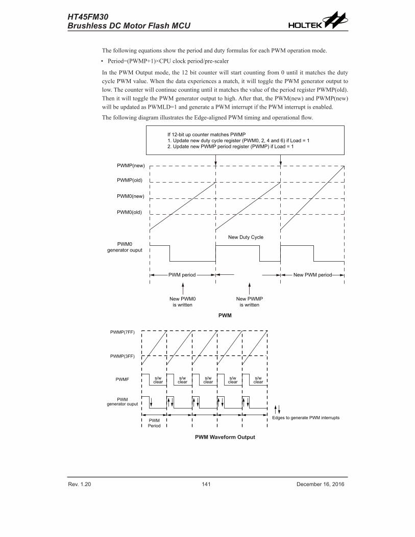
Rev. 1.20 140 De�e��e� 1�� 201� Rev. 1.20 141 De�e��e� 1�� 201�
HT45FM30Brushless DC Motor Flash MCU
ThefollowingequationsshowtheperiodanddutyformulasforeachPWMoperationmode.
• Period=(PWMP+1)×CPUclockperiod/pre-scaler
InthePWMOutputmode,the12bitcounterwillstartcountingfrom0until itmatchesthedutycyclePWMvalue.Whenthedataexperiencesamatch,itwilltogglethePWMgeneratoroutputtolow.ThecounterwillcontinuecountinguntilitmatchesthevalueoftheperiodregisterPWMP(old).ThenitwilltogglethePWMgeneratoroutputtohigh.Afterthat,thePWM(new)andPWMP(new)willbeupdatedasPWMLD=1andgenerateaPWMinterruptifthePWMinterruptisenabled.
ThefollowingdiagramillustratestheEdge-alignedPWMtimingandoperationalflow.
PWMP(new)
If 12-bit up counter matches PWMP1. Update new duty cycle register (PWM0, 2, 4 and 6) if Load = 12. Update new PWMP period register (PWMP) if Load = 1
PWMP(old)
PWM0(new)
PWM0(old)
PWM period
New PWM0is written
New PWMPis written
New Duty Cycle
New PWM period
PWM0generator ouput
PWM
PWMP(7FF)
PWMP(3FF)
PWMF s/wclear
s/wclear
s/wclear
s/wclear
s/wclear
PWMPeriod
PWMgenerator ouput
Edges to generate PWM interrupts
PWM Waveform Output
Rev. 1.20 142 De�e��e� 1�� 201� Rev. 1.20 143 De�e��e� 1�� 201�
HT45FM30Brushless DC Motor Flash MCU
PWM Output ControlThereareatotalofsixPWMpins,dividedintothreepairsofcomplimentaryPWMoutputs.ThePWMoutputsarecontrolledusingregisterbits.ThePWMoutputscanbeeitherasingleoutput,PWMH,oracomplimentarypairofoutputs,PWMnHandPWMnL.BoththePWMnHandPWMnLoutputscanbesettobeeitheractivehighoractivelowusingsoftwareoptions.
ThePWMoutputportswilldefaulttofloatingtypesafterareset.
I/O Pin PWM LinePB3 PWM0HPB4 PWM0L
PB5 o� PA3 PWM1HPA4 PWM1L
PA5 o� PC2 PWM2HPA� o� PC3 PWM2L
ThePWMENbitinthePWMC0registeractsasamastercontrolbitforthePWMoutputs.WhenthisbitishightheselectedPWMoutputswillbeactiveandwhenthebitislowallthePWMoutputswillhaveotherfunctions.ThethreePWMpinsPWM0H,PWM1HandPWM2Hhaveacontrolbit,PWMEN,andthecomplementaryPWMpins,PWM0L,PWM1LandPWM2L,haveacontrolbit,PWMCEN.WhenthesebitsaresettohightheirthreecorrespondingPWMpinswillbeactive,whenthebitsareclearedtozerotheirPWMpinswillbesettotheinactivestateasdefinedbysoftwareoptions.
AsnotallofthePWMmayberequired,thedevicesoffertheflexibilitytoselectwhichpinsareusedasPWMpinsandwhichpinsareusedasI/Opins.ThisisdeterminedeitherbybitsinthePWMC1andPWMC2registers.ThefollowingtableillustratesthePWMI/Oselection.
PWM0H, PWM1H, PWM2H selection table
PWMEN PnHEN I/O or PWM0 0 I/O0 1 I/O1 0 I/O1 1 PWMnH
PWM0L, PWM1L, PWM2L selection table
PWMCEN PnLEN I/O or PWM0 0 I/O0 1 I/O1 0 I/O1 1 PWMnL
EachPWMandcomplementaryPWMhasacorrespondingcontrolbittoselectenableordisable.
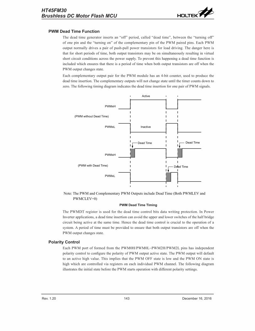
Rev. 1.20 142 De�e��e� 1�� 201� Rev. 1.20 143 De�e��e� 1�� 201�
HT45FM30Brushless DC Motor Flash MCU
PWM Dead Time FunctionThedead timegenerator insertsan“off”period,called“dead time”,between the“turningoff”ofonepinandthe“turningon”of thecomplementarypinof thePWMpairedpins.EachPWMoutputnormallydrivesapairofpush-pullpowertransistorsfor loaddriving.Thedangerhere isthatforshortperiodsoftime,bothoutputtransistorsmaybeonsimultaneouslyresultinginvirtualshortcircuitconditionsacrossthepowersupply.TopreventthishappeningadeadtimefunctionisincludedwhichensuresthatthereisaperiodoftimewhenbothoutputtransistorsareoffwhenthePWMoutputchangesstate.
Eachcomplementaryoutputpairfor thePWMmodulehasan4-bitcounter,usedtoproducethedeadtimeinsertion.Thecomplementaryoutputswillnotchangestateuntilthetimercountsdowntozero.ThefollowingtimingdiagramindicatesthedeadtimeinsertionforonepairofPWMsignals.
PWMxH
(PWM without Dead Time)
PWMxL
PWMxH
(PWM with Dead Time)
PWMxL
Dead Time
Active
Inactive
Dead Time
Dead Time
Note:ThePWMandComplementaryPWMOutputsincludeDeadTime(BothPWMLEVandPWMCLEV=0)
PWM Dead Time Timing
ThePWMDTregister isused for thedead timecontrolbitsdatawritingprotection. InPowerInverterapplications,adeadtimeinsertioncanavoidtheupperandlowerswitchesofthehalfbridgecircuitbeingactiveat thesametime.Hencethedeadtimecontroliscrucial totheoperationofasystem.AperiodoftimemustbeprovidedtoensurethatbothoutputtransistorsareoffwhenthePWMoutputchangesstate.
Polarity ControlEachPWMportofformedfromthePWM0H/PWM0L~PWM2H/PWM2Lpinshas independentpolaritycontroltoconfigurethepolarityofPWMoutputactivestate.ThePWMoutputwilldefaulttoanactivehighvalue.This implies that thePWMOFFstate is lowandthePWMONstate ishighwhicharecontrolledviaregistersoneachindividualPWMchannel.ThefollowingdiagramillustratestheinitialstatebeforethePWMstartsoperationwithdifferentpolaritysettings.
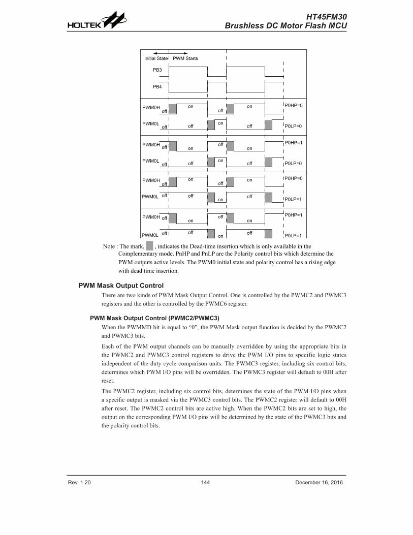
Rev. 1.20 144 De�e��e� 1�� 201� Rev. 1.20 145 De�e��e� 1�� 201�
HT45FM30Brushless DC Motor Flash MCU
PWM0H P0HP=0
P0LP=0PWM0L on
on onoff
off off
off
off
Initial State PWM Starts
PB3
PB4
PWM0H P0HP=1on on
offoff
P0LP=0PWM0L onoff offoff
PWM0H P0HP=0on onoffoff
P0LP=1PWM0L onoff offoff
PWM0H P0HP=1on on
offoff
P0LP=1PWM0L onoff offoff
Note:Themark, ,indicatestheDead-timeinsertionwhichisonlyavailableintheComplementarymode.PnHPandPnLParethePolaritycontrolbitswhichdeterminethePWMoutputsactivelevels.ThePWM0initialstateandpolaritycontrolhasarisingedgewithdeadtimeinsertion.
PWM Mask Output ControlTherearetwokindsofPWMMaskOutputControl.OneiscontrolledbythePWMC2andPWMC3registersandtheotheriscontrolledbythePWMC6register.
PWM Mask Output Control (PWMC2/PWMC3)WhenthePWMMDbitisequalto“0”,thePWMMaskoutputfunctionisdecidedbythePWMC2andPWMC3bits.
Eachof thePWMoutputchannelscanbemanuallyoverriddenbyusing theappropriatebits inthePWMC2andPWMC3control registers todrive thePWMI/Opins tospecific logicstatesindependentofthedutycyclecomparisonunits.ThePWMC3register, includingsixcontrolbits,determineswhichPWMI/Opinswillbeoverridden.ThePWMC3registerwilldefaultto00Hafterreset.
ThePWMC2register, includingsixcontrolbits,determinesthestateofthePWMI/OpinswhenaspecificoutputismaskedviathePWMC3controlbits.ThePWMC2registerwilldefaultto00Hafterreset.ThePWMC2controlbitsareactivehigh.WhenthePWMC2bitsareset tohigh, theoutputonthecorrespondingPWMI/OpinswillbedeterminedbythestateofthePWMC3bitsandthepolaritycontrolbits.
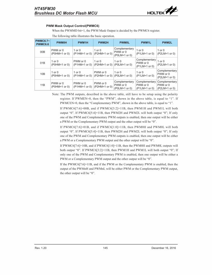
Rev. 1.20 144 De�e��e� 1�� 201� Rev. 1.20 145 De�e��e� 1�� 201�
HT45FM30Brushless DC Motor Flash MCU
PWM Mask Output Control(PWMC6)WhenthePWMMDbit=1,thePWMMaskOutputisdecidedbythePWMC6register.
Thefollowingtableillustratesthebasicoperation.PWMC6.7~ PWMC6.6 PWM0H PWM1H PWM2H PWM0L PWM1L PWM2L
00B PWM o� 0 (P0HM=1 o� 0)
1 o� 0 (P1HM=1 o� 0)
1 o� 0 (P2HM=1 o� 0)
Co�ple�enta�y PWM o� 0 (P0LM=1 o� 0)
1 o� 0 (P1LM=1 o� 0)
1 o� 0 (P2LM=1 o� 0)
01B 1 o� 0 (P0HM=1 o� 0)
PWM o� 0 (P1HM=1 o� 0)
1 o� 0 (P2HM=1 o� 0)
1 o� 0 (P0LM=1 o� 0)
Co�ple�enta�y PWM o� 0 (P1LM=1 o� 0)
1 o� 0 (P2LM=1 o� 0)
10B 1 o� 0 (P0HM=1 o� 0)
1 o� 0 (P1HM=1 o� 0)
PWM o� 0(P2HM=1 o� 0)
1 o� 0 (P0LM=1 o� 0)
1 o� 0 (P1LM=1 o� 0)
Co�ple�enta�y PWM o� 0 (P2LM=1 o� 0)
11B PWM o� 0 (P0HM=1 o� 0)
PWM o� 0 (P1HM=1 o� 0)
PWM o� 0(P2HM=1 o� 0)
Co�ple�enta�y PWM o� 0 (P0LM=1 o� 0)
Co�ple�enta�y PWM o� 0 (P1LM=1 o� 0)
Co�ple�enta�y PWM o� 0 (P2LM=1 o� 0)
Note:ThePWMoutputs,described in theabove table,stillhave tobesetupusing thepolarityregister. IfPWMEN=0, then the“PWM”,shown in theabove table, is equal to“1”. IfPWMCEN=0,thenthe“ComplementaryPWM”,shownintheabovetable,isequalto“1”.
IfPWMC6[7:6]=00B,and ifPWMC6[3:2]=11B, thenPWM1HandPWM1Lwillbothoutput“0”.IfPWMC6[5:4]=11B,thenPWM2HandPWM2Lwillbothoutput“0”;IfonlyoneofthePWMandComplementaryPWMoutputsisenabled,thenoneoutputwillbeeitheraPWMortheComplementaryPWMoutputandtheotheroutputwillbe“0”.
IfPWMC6[7:6]=01B,and ifPWMC6[1:0]=11B, thenPWM0HandPWM0Lwillbothoutput“0”.IfPWMC6[5:4]=11B,thenPWM2HandPWM2Lwillbothoutput“0”;IfonlyoneofthePWMandComplementaryPWMoutputsisenabled,thenoneoutputwillbeeitheraPWMoraComplementaryPWMoutputandtheotheroutputwillbe“0”.
IfPWMC6[7:6]=10B,andifPWMC6[1:0]=11B,thenthePWM0HandPWM0Loutputswillbothoutput“0”.IfPWMC6[3:2]=11B,thenPWM1HandPWM1Lwillbothoutput“0”;IfonlyoneofthePWMandComplementaryPWMisenabled,thenoneoutputwillbeeitheraPWMoraComplementaryPWMoutputandtheotheroutputwillbe“0”.
IfthePWMC6[7:6]=11B,andifthePWMortheComplementaryPWMisenabled,thentheoutputofthePWMnHandPWMnLwillbeeitherPWMortheComplementaryPWMoutput,theotheroutputwillbe“0”.
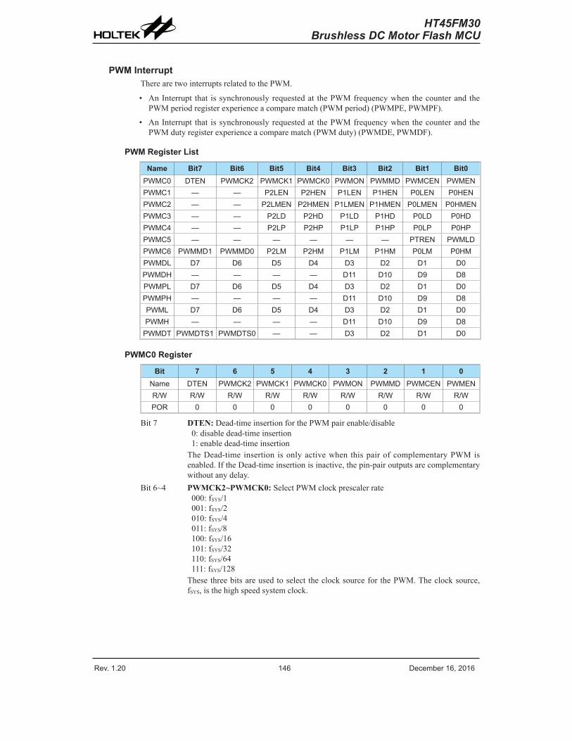
Rev. 1.20 14� De�e��e� 1�� 201� Rev. 1.20 147 De�e��e� 1�� 201�
HT45FM30Brushless DC Motor Flash MCU
PWM InterruptTherearetwointerruptsrelatedtothePWM.
• AnInterrupt that issynchronouslyrequestedat thePWMfrequencywhenthecounterandthePWMperiodregisterexperienceacomparematch(PWMperiod)(PWMPE,PWMPF).
• AnInterrupt that issynchronouslyrequestedat thePWMfrequencywhenthecounterandthePWMdutyregisterexperienceacomparematch(PWMduty)(PWMDE,PWMDF).
PWM Register List
Name Bit7 Bit6 Bit5 Bit4 Bit3 Bit2 Bit1 Bit0PWMC0 DTEN PWMCK2 PWMCK1 PWMCK0 PWMON PWMMD PWMCEN PWMENPWMC1 — — P2LEN P2HEN P1LEN P1HEN P0LEN P0HENPWMC2 — — P2LMEN P2HMEN P1LMEN P1HMEN P0LMEN P0HMENPWMC3 — — P2LD P2HD P1LD P1HD P0LD P0HDPWMC4 — — P2LP P2HP P1LP P1HP P0LP P0HPPWMC5 — — — — — — PTREN PWMLDPWMC� PWMMD1 PWMMD0 P2LM P2HM P1LM P1HM P0LM P0HMPWMDL D7 D� D5 D4 D3 D2 D1 D0PWMDH — — — — D11 D10 D9 D8PWMPL D7 D� D5 D4 D3 D2 D1 D0PWMPH — — — — D11 D10 D9 D8PWML D7 D� D5 D4 D3 D2 D1 D0PWMH — — — — D11 D10 D9 D8
PWMDT PWMDTS1 PWMDTS0 — — D3 D2 D1 D0
PWMC0 Register
Bit 7 6 5 4 3 2 1 0Na�e DTEN PWMCK2 PWMCK1 PWMCK0 PWMON PWMMD PWMCEN PWMENR/W R/W R/W R/W R/W R/W R/W R/W R/WPOR 0 0 0 0 0 0 0 0
Bit7 DTEN:Dead-timeinsertionforthePWMpairenable/disable0:disabledead-timeinsertion1:enabledead-timeinsertionTheDead-time insertion isonlyactivewhen thispairofcomplementaryPWMisenabled.IftheDead-timeinsertionisinactive,thepin-pairoutputsarecomplementarywithoutanydelay.
Bit6~4 PWMCK2~PWMCK0:SelectPWMclockprescalerrate000:fSYS/1001:fSYS/2010:fSYS/4011:fSYS/8100:fSYS/16101:fSYS/32110:fSYS/64111:fSYS/128ThesethreebitsareusedtoselecttheclocksourceforthePWM.Theclocksource,fSYS,isthehighspeedsystemclock.
Rev. 1.20 14� De�e��e� 1�� 201� Rev. 1.20 147 De�e��e� 1�� 201�
HT45FM30Brushless DC Motor Flash MCU
Bit3 PWMON:PWMoutputOn/OffControl0:off1:onThisbitisusedtocontroltheoverallon/offfunctionofthePWM.SettingthebithighwillenablethePWMtorunandclearingthebitwilldisablethePWM.Clearingthisbittozerowillstopthecounter.
Bit2 PWMMD:PWMOutputMaskModeselection0:maskbyPWMC2andPWMC31:maskbyPWMC6
Bit1 PWMCEN:ComplementaryPWMsignalenable/disablecontrol0:complementaryPWMsignaldisable1:complementaryPWMsignalenable
Bit0 PWMEN:PWMsignalenable/disablecontrol0:PWMsignaldisable1:PWMsignalenable
PWMC1 Register
Bit 7 6 5 4 3 2 1 0Na�e — — P2LEN P2HEN P1LEN P1HEN P0LEN P0HENR/W — — R/W R/W R/W R/W R/W R/WPOR — — 0 0 0 0 0 0
Bit7~6 Unimplemented,readas"0"Bit5 P2LEN:PWM2Loutputenable/disable
0:disable1:enable
Bit4 P2HEN:PWM2Houtputenable/disable0:disable1:enable
Bit3 P1LEN:PWM1Loutputenable/disable0:disable1:enable
Bit2 P1HEN:PWM1Houtputenable/disable0:disable1:enable
Bit1 P0LEN:PWM0Loutputenable/disable0:disable1:enable
Bit0 P0HEN:PWM0Houtputenable/disable0:disable1:enable
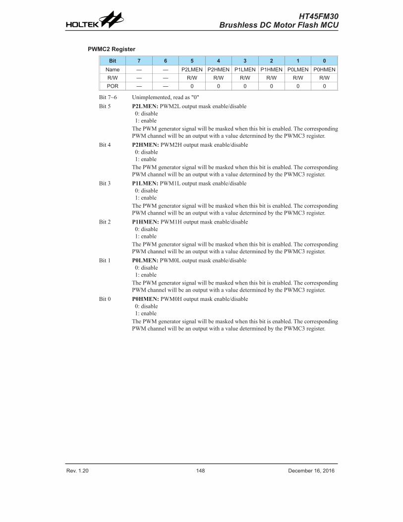
Rev. 1.20 148 De�e��e� 1�� 201� Rev. 1.20 149 De�e��e� 1�� 201�
HT45FM30Brushless DC Motor Flash MCU
PWMC2 Register
Bit 7 6 5 4 3 2 1 0Na�e — — P2LMEN P2HMEN P1LMEN P1HMEN P0LMEN P0HMENR/W — — R/W R/W R/W R/W R/W R/WPOR — — 0 0 0 0 0 0
Bit7~6 Unimplemented,readas"0"Bit5 P2LMEN:PWM2Loutputmaskenable/disable
0:disable1:enableThePWMgeneratorsignalwillbemaskedwhenthisbitisenabled.ThecorrespondingPWMchannelwillbeanoutputwithavaluedeterminedbythePWMC3register.
Bit4 P2HMEN:PWM2Houtputmaskenable/disable0:disable1:enableThePWMgeneratorsignalwillbemaskedwhenthisbitisenabled.ThecorrespondingPWMchannelwillbeanoutputwithavaluedeterminedbythePWMC3register.
Bit3 P1LMEN:PWM1Loutputmaskenable/disable0:disable1:enableThePWMgeneratorsignalwillbemaskedwhenthisbitisenabled.ThecorrespondingPWMchannelwillbeanoutputwithavaluedeterminedbythePWMC3register.
Bit2 P1HMEN:PWM1Houtputmaskenable/disable0:disable1:enableThePWMgeneratorsignalwillbemaskedwhenthisbitisenabled.ThecorrespondingPWMchannelwillbeanoutputwithavaluedeterminedbythePWMC3register.
Bit1 P0LMEN:PWM0Loutputmaskenable/disable0:disable1:enableThePWMgeneratorsignalwillbemaskedwhenthisbitisenabled.ThecorrespondingPWMchannelwillbeanoutputwithavaluedeterminedbythePWMC3register.
Bit0 P0HMEN:PWM0Houtputmaskenable/disable0:disable1:enableThePWMgeneratorsignalwillbemaskedwhenthisbitisenabled.ThecorrespondingPWMchannelwillbeanoutputwithavaluedeterminedbythePWMC3register.
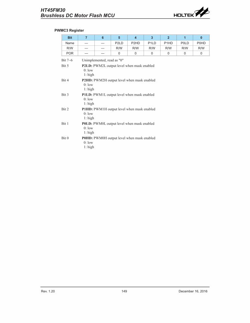
Rev. 1.20 148 De�e��e� 1�� 201� Rev. 1.20 149 De�e��e� 1�� 201�
HT45FM30Brushless DC Motor Flash MCU
PWMC3 Register
Bit 7 6 5 4 3 2 1 0Na�e — — P2LD P2HD P1LD P1HD P0LD P0HDR/W — — R/W R/W R/W R/W R/W R/WPOR — — 0 0 0 0 0 0
Bit7~6 Unimplemented,readas"0"Bit5 P2LD:PWM2Loutputlevelwhenmaskenabled
0:low1:high
Bit4 P2HD:PWM2Houtputlevelwhenmaskenabled0:low1:high
Bit3 P1LD:PWM1Loutputlevelwhenmaskenabled0:low1:high
Bit2 P1HD:PWM1Houtputlevelwhenmaskenabled0:low1:high
Bit1 P0LD:PWM0Loutputlevelwhenmaskenabled0:low1:high
Bit0 P0HD:PWM0Houtputlevelwhenmaskenabled0:low1:high
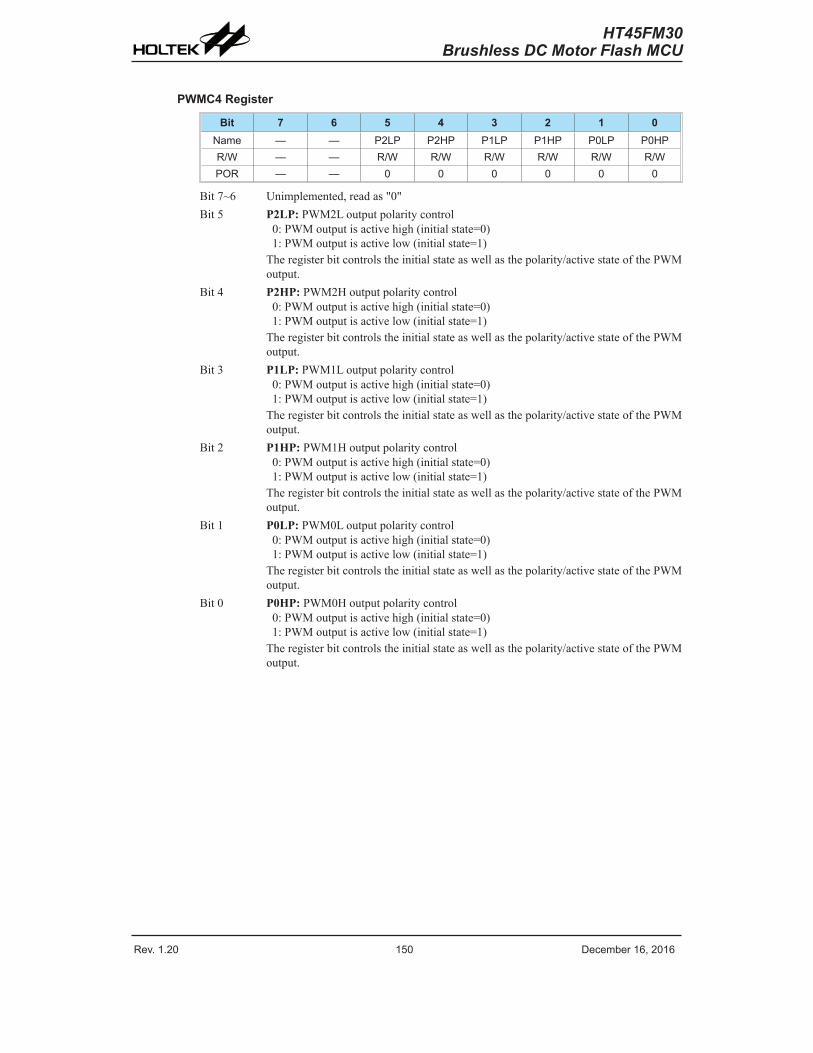
Rev. 1.20 150 De�e��e� 1�� 201� Rev. 1.20 151 De�e��e� 1�� 201�
HT45FM30Brushless DC Motor Flash MCU
PWMC4 Register
Bit 7 6 5 4 3 2 1 0Na�e — — P2LP P2HP P1LP P1HP P0LP P0HPR/W — — R/W R/W R/W R/W R/W R/WPOR — — 0 0 0 0 0 0
Bit7~6 Unimplemented,readas"0"Bit5 P2LP:PWM2Loutputpolaritycontrol
0:PWMoutputisactivehigh(initialstate=0)1:PWMoutputisactivelow(initialstate=1)Theregisterbitcontrolstheinitialstateaswellasthepolarity/activestateofthePWMoutput.
Bit4 P2HP:PWM2Houtputpolaritycontrol0:PWMoutputisactivehigh(initialstate=0)1:PWMoutputisactivelow(initialstate=1)Theregisterbitcontrolstheinitialstateaswellasthepolarity/activestateofthePWMoutput.
Bit3 P1LP:PWM1Loutputpolaritycontrol0:PWMoutputisactivehigh(initialstate=0)1:PWMoutputisactivelow(initialstate=1)Theregisterbitcontrolstheinitialstateaswellasthepolarity/activestateofthePWMoutput.
Bit2 P1HP:PWM1Houtputpolaritycontrol0:PWMoutputisactivehigh(initialstate=0)1:PWMoutputisactivelow(initialstate=1)Theregisterbitcontrolstheinitialstateaswellasthepolarity/activestateofthePWMoutput.
Bit1 P0LP:PWM0Loutputpolaritycontrol0:PWMoutputisactivehigh(initialstate=0)1:PWMoutputisactivelow(initialstate=1)Theregisterbitcontrolstheinitialstateaswellasthepolarity/activestateofthePWMoutput.
Bit0 P0HP:PWM0Houtputpolaritycontrol0:PWMoutputisactivehigh(initialstate=0)1:PWMoutputisactivelow(initialstate=1)Theregisterbitcontrolstheinitialstateaswellasthepolarity/activestateofthePWMoutput.
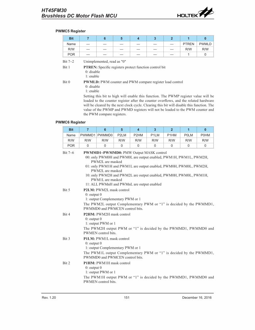
Rev. 1.20 150 De�e��e� 1�� 201� Rev. 1.20 151 De�e��e� 1�� 201�
HT45FM30Brushless DC Motor Flash MCU
PWMC5 Register
Bit 7 6 5 4 3 2 1 0Na�e — — — — — — PTREN PWMLDR/W — — — — — — R/W R/WPOR — — — — — — 1 0
Bit7~2 Unimplemented,readas"0"Bit1 PTREN:Specificregistersprotectfunctioncontrolbit
0:disable1:enable
Bit0 PWMLD:PWMcounterandPWMcompareregisterloadcontrol0:disable1:enableSettingthisbit tohighwillenablethisfunction.ThePWMPregistervaluewillbeloadedtothecounterregisterafter thecounteroverflows,andtherelatedhardwarewillbeclearedbythenextclockcycle.Clearingthisbitwilldisablethisfunction.ThevalueofthePWMPandPWMDregisterswillnotbeloadedtothePWMcounterandthePWMcompareregisters.
PWMC6 Register
Bit 7 6 5 4 3 2 1 0Na�e PWMMD1 PWMMD0 P2LM P2HM P1LM P1HM P0LM P0HMR/W R/W R/W R/W R/W R/W R/W R/W R/WPOR 0 0 0 0 0 0 0 0
Bit7~6 PWMMD1~PWMMD0:PMWOutputMASKcontrol00:onlyPWM0HandPWM0Lareoutputenabled,PWM1H,PWM1L,PWM2H,PWM2Laremasked01:onlyPWM1HandPWM1Lareoutputenabled,PWM0H,PWM0L,PWM2H,PWM2Laremasked10:onlyPWM2HandPWM2Lareoutputenabled,PWM0H,PWM0L,PWM1H,PWM1Laremasked11:ALLPWMnHandPWMnLareoutputenabled
Bit5 P2LM:PWM2Lmaskcontrol0:output01:outputComplementaryPWMor1ThePWM2LoutputComplementaryPWMor“1” isdecidedby thePWMMD1,PWMMD0andPWMCENcontrolbits.
Bit4 P2HM:PWM2Hmaskcontrol0:output01:outputPWMor1ThePWM2HoutputPWMor“1” isdecidedby thePWMMD1,PWMMD0andPWMENcontrolbits.
Bit3 P1LM:PWM1Lmaskcontrol0:output01:outputComplementaryPWMor1ThePWM1LoutputComplementaryPWMor“1” isdecidedby thePWMMD1,PWMMD0andPWMCENcontrolbits.
Bit2 P1HM:PWM1Hmaskcontrol0:output01:outputPWMor1ThePWM1HoutputPWMor“1” isdecidedby thePWMMD1,PWMMD0andPWMENcontrolbits.
Rev. 1.20 152 De�e��e� 1�� 201� Rev. 1.20 153 De�e��e� 1�� 201�
HT45FM30Brushless DC Motor Flash MCU
Bit1 P0LM:PWM0Lmaskcontrol0:output01:outputComplementaryPWMor1ThePWM0LoutputComplementaryPWMor“1” isdecidedby thePWMMD1,PWMMD0andPWMCENcontrolbits.
Bit0 P0HM:PWM0Hmaskcontrol0:output01:outputPWMor1ThePWM0HoutputPWMor“1” isdecidedby thePWMMD1,PWMMD0andPWMENcontrolbits.
PWMDL Register
Bit 7 6 5 4 3 2 1 0Na�e D7 D� D5 D4 D3 D2 D1 D0R/W R R R R R R R RPOR 0 0 0 0 0 0 0 0
Bit7~0 PWMDL:PWMCounterLowByteRegisterbit7~bit0PWM12-bitCounterbit7~bit0
PWMDH Register
Bit 7 6 5 4 3 2 1 0Na�e — — — — D11 D10 D9 D8R/W — — — — R R R RPOR — — — — 0 0 0 0
Bit7~4 Unimplemented,readas"0"Bit3~0 PWMDH:PWMCounterHighByteRegisterbit3~bit0
PWM12-bitCounterbit11~bit8
PWMPL Register
Bit 7 6 5 4 3 2 1 0Na�e D7 D� D5 D4 D3 D2 D1 D0R/W R/W R/W R/W R/W R/W R/W R/W R/WPOR 0 0 0 0 0 0 0 0
Bit7~0 PWMPL:PWMPeriodLowByteRegisterbit7~bit0PWMP12-bitRegisterbit7~bit0
PWMPH Register
Bit 7 6 5 4 3 2 1 0Na�e — — — — D11 D10 D9 D8R/W — — — — R/W R/W R/W R/WPOR — — — — 0 0 0 0
Bit7~4 Unimplemented,readas"0"Bit3~0 PWMPH.3~PWMPH.0:PWMPeriodHighByteRegisterbit3~bit0
PWMP12-bitRegisterbit11~bit8
Rev. 1.20 152 De�e��e� 1�� 201� Rev. 1.20 153 De�e��e� 1�� 201�
HT45FM30Brushless DC Motor Flash MCU
PWML Register
Bit 7 6 5 4 3 2 1 0Na�e D7 D� D5 D4 D3 D2 D1 D0R/W R/W R/W R/W R/W R/W R/W R/W R/WPOR 0 0 0 0 0 0 0 0
Bit7~0 PWML:PWMDutyLowByteRegisterbit7~bit0PWM12-bitDutySettingRegisterbit7~bit0
PWMH Register
Bit 7 6 5 4 3 2 1 0Na�e — — — — D11 D10 D9 D8R/W — — — — R/W R/W R/W R/WPOR — — — — 0 0 0 0
Bit7~4 Unimplemented,readas"0"Bit3~0 PWMH.3~PWMH.0:PWMDutyHighByteRegisterbit3~bit0
PWM12-bitDutySettingRegisterbit11~bit8
PWMDT Register
Bit 7 6 5 4 3 2 1 0Na�e PWMDTS1 PWMDTS0 — — D3 D2 D1 D0R/W R/W R/W — — R/W R/W R/W R/WPOR 0 0 — — 0 0 0 0
Bit7~6 PWMDT:PWMDeadTimeclocksourceselection00:fPWMDTisfSYS/101:fPWMDTisfSYS/210:fPWMDTisfSYS/411:fPWMDTisfSYS/8
Bit5~4 Unimplemented,readas"0"Bit3~0 PWMDT:PWMDeadTimeRegisterbit3~bit0
Dead-timecounter,4-bitdeadtimevaluebitsforDeadTimeUnitPWMDead-time=(PWMDT.3~0+1)/fPWMDT
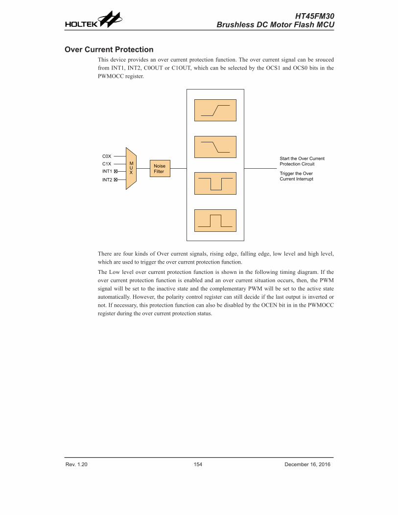
Rev. 1.20 154 De�e��e� 1�� 201� Rev. 1.20 155 De�e��e� 1�� 201�
HT45FM30Brushless DC Motor Flash MCU
Over Current ProtectionThisdeviceprovidesanovercurrentprotectionfunction.TheovercurrentsignalcanbesroucedfromINT1,INT2,C0OUTorC1OUT,whichcanbeselectedbytheOCS1andOCS0bitsinthePWMOCCregister.
INT1
INT2
C1X
C0XMUX
NoiseFilter
Start the Over CurrentProtection Circuit
Trigger the OverCurrent Interrupt
TherearefourkindsofOvercurrentsignals,risingedge,fallingedge, lowlevelandhighlevel,whichareusedtotriggertheovercurrentprotectionfunction.
TheLowlevelovercurrentprotectionfunctionisshowninthefollowingtimingdiagram.If theovercurrentprotectionfunction isenabledandanovercurrentsituationoccurs, then, thePWMsignalwillbesettotheinactivestateandthecomplementaryPWMwillbesettotheactivestateautomatically.However,thepolaritycontrolregistercanstilldecideifthelastoutputisinvertedornot.Ifnecessary,thisprotectionfunctioncanalsobedisabledbytheOCENbitininthePWMOCCregisterduringtheovercurrentprotectionstatus.
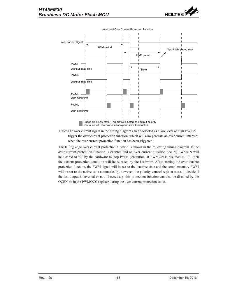
Rev. 1.20 154 De�e��e� 1�� 201� Rev. 1.20 155 De�e��e� 1�� 201�
HT45FM30Brushless DC Motor Flash MCU
over current signal
PWM period
PWM period
New PWM period start
*Note
Low Level Over Current Protection Function
PWMH
PWMH
PWML
PWML
Without dead time
Without dead time
With dead time
With dead time
: Dead time, Low state, This profile is before the output polarity control circuit. The over current signal is low level active.
Note:Theovercurrentsignalinthetimingdiagramcanbeselectedasalowlevelorhighleveltotriggertheovercurrentprotectionfunction,whichwillalsogenerateanovercurrentinterruptwhentheovercurrentprotectionfunctionhasbeentriggered.
Thefallingedgeovercurrentprotectionfunctionisshowninthefollowingtimingdiagram.Iftheovercurrentprotectionfunction isenabledandanovercurrentsituationoccurs,PWMONwillbeclearedto“0”bythehardwaretostopPWMgeneration.IfPWMONisresumedto“1”, thenthecurrentprotectionconditionwillbereleasedbythehardware.Afterstartingtheovercurrentprotectionfunction,thePWMsignalwillbesettotheinactivestateandthecomplementaryPWMwillbesettotheactivestateautomatically,however,thepolaritycontrolregistercanstilldecideifthelastoutputisinvertedornot.Ifnecessary,thisprotectionfunctioncanalsobedisabledbytheOCENbitinthePWMOCCregisterduringtheovercurrentprotectionstatus.
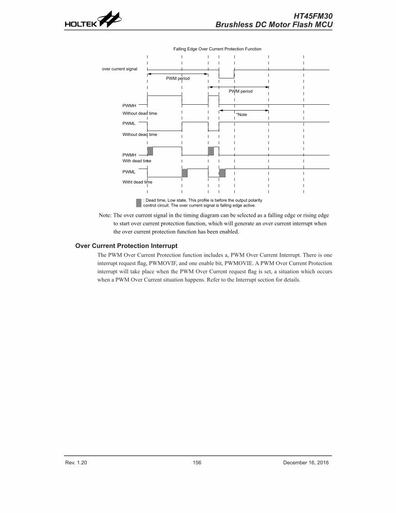
Rev. 1.20 15� De�e��e� 1�� 201� Rev. 1.20 157 De�e��e� 1�� 201�
HT45FM30Brushless DC Motor Flash MCU
over current signal
PWM period
PWM period
*Note
Falling Edge Over Current Protection Function
PWMH
PWMH
PWML
PWML
Without dead time
Without dead time
With dead time
Witht dead time
: Dead time, Low state, This profile is before the output polarity control circuit. The over current signal is falling edge active.
Note:Theovercurrentsignalinthetimingdiagramcanbeselectedasafallingedgeorrisingedgetostartovercurrentprotectionfunction,whichwillgenerateanovercurrentinterruptwhentheovercurrentprotectionfunctionhasbeenenabled.
Over Current Protection InterruptThePWMOverCurrentProtectionfunctionincludesa,PWMOverCurrentInterrupt.Thereisoneinterruptrequestflag,PWMOVIF,andoneenablebit,PWMOVIE.APWMOverCurrentProtectioninterruptwilltakeplacewhenthePWMOverCurrentrequestflagisset,asituationwhichoccurswhenaPWMOverCurrentsituationhappens.RefertotheInterruptsectionfordetails.
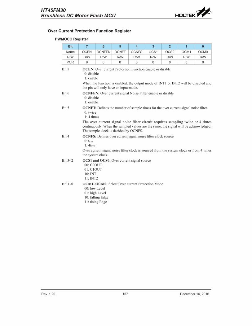
Rev. 1.20 15� De�e��e� 1�� 201� Rev. 1.20 157 De�e��e� 1�� 201�
HT45FM30Brushless DC Motor Flash MCU
Over Current Protection Function Register
PWMOCC Register
Bit 7 6 5 4 3 2 1 0Na�e OCEN OCNFEN OCNFT OCNFS OCS1 OCS0 OCM1 OCM0R/W R/W R/W R/W R/W R/W R/W R/W R/WPOR 0 0 0 0 0 0 0 0
Bit7 OCEN:OvercurrentProtectionFunctionenableordisable0:disable1:enableWhenthefunctionisenabled,theoutputmodeofINT1orINT2willbedisabledandthepinwillonlyhaveaninputmode.
Bit6 OCNFEN: OvercurrentsignalNoiseFilterenableordisable0:disable1:enable
Bit5 OCNFT:Definesthenumberofsampletimesfortheovercurrentsignalnoisefilter0:twice1:4timesTheover current signalnoise filter circuit requires sampling twiceor4 timescontinuously.Whenthesampledvaluesarethesame,thesignalwillbeacknowledged.ThesampleclockisdecidedbyOCNFS.
Bit4 OCNFS:Definesovercurrentsignalnoisefilterclocksource0:tSYS
1:4tSYS
Overcurrentsignalnoisefilterclockissourcedfromthesystemclockorfrom4timesthesystemclock.
Bit3~2 OCS1 and OCS0:Overcurrentsignalsource00:C0OUT01:C1OUT10:INT111:INT2
Bit1~0 OCM1~OCM0:SelectOvercurrentProtectionMode00:lowLevel01:highLevel10:fallingEdge11:risingEdge
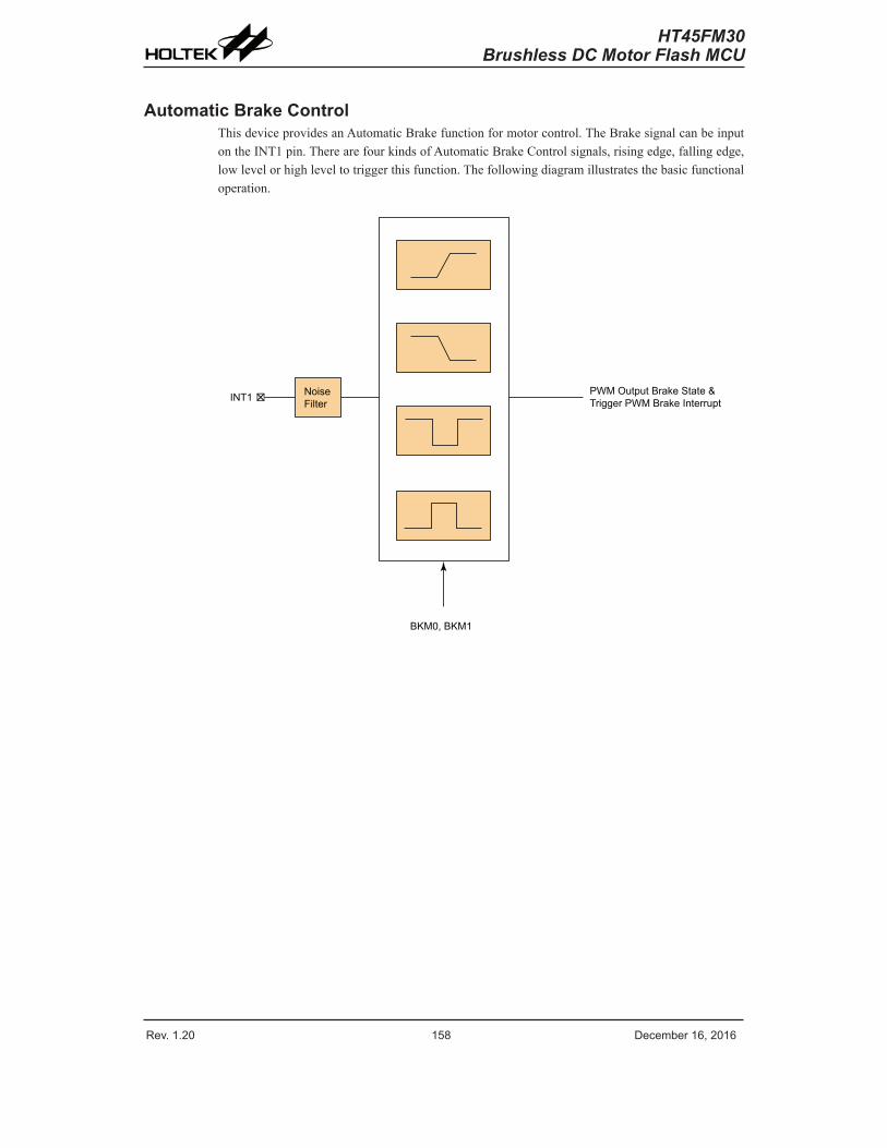
Rev. 1.20 158 De�e��e� 1�� 201� Rev. 1.20 159 De�e��e� 1�� 201�
HT45FM30Brushless DC Motor Flash MCU
Automatic Brake ControlThisdeviceprovidesanAutomaticBrakefunctionformotorcontrol.TheBrakesignalcanbeinputontheINT1pin.TherearefourkindsofAutomaticBrakeControlsignals,risingedge,fallingedge,lowlevelorhighleveltotriggerthisfunction.Thefollowingdiagramillustratesthebasicfunctionaloperation.
INT1 NoiseFilter
PWM Output Brake State &Trigger PWM Brake Interrupt
BKM0, BKM1
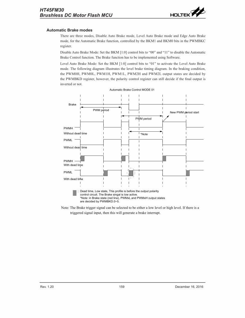
Rev. 1.20 158 De�e��e� 1�� 201� Rev. 1.20 159 De�e��e� 1�� 201�
HT45FM30Brushless DC Motor Flash MCU
Automatic Brake modesTherearethreemodes,DisableAutoBrakemode,LevelAutoBrakemodeandEdgeAutoBrakemode,fortheAutomaticBrakefunction,controlledbytheBKM1andBKM0bitsinthePWMBKCregister.
DisableAutoBrakeMode:SettheBKM[1:0]controlbitsto“00”and“11”todisabletheAutomaticBrakeControlfunction.TheBrakefunctionhastobeimplementedusingSoftware.
LevelAutoBrakeMode:SettheBKM[1:0]controlbitsto“01”toactivatetheLevelAutoBrakemode.Thefollowingdiagramillustratesthelevelbraketimingdiagram.Inthebrakingcondition,thePWM0H,PWM0L,PWM1H,PWM1L,PWM2HandPWM2LoutputstatesaredecidedbythePWMBKDregister,however, thepolaritycontrolregistercanstilldecideif thefinaloutputisinvertedornot.
Brake
PWM period
PWM period
New PWM period start
*Note
Automatic Brake Control MODE 01
PWMH
PWMH
PWML
PWML
Without dead time
Without dead time
With dead time
With dead time
: Dead time, Low state, This profile is before the output polarity control circuit. The Brake singal is low active. *Note: in Brake state (red line), PWMxL and PWMxH output states are decided by PWMBKD.0~5.
Note:TheBraketriggersignalcanbeselectedtobeeitheralowlevelorhighlevel.Ifthereisatriggeredsignalinput,thenthiswillgenerateabrakeinterrupt.
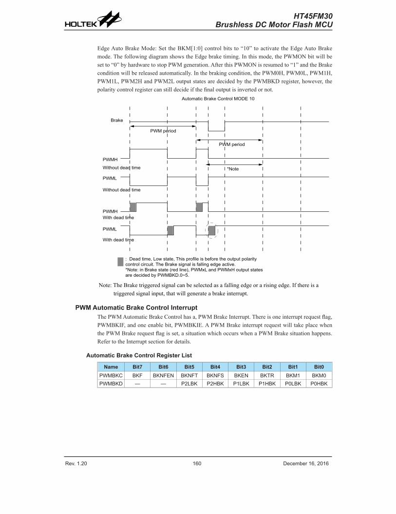
Rev. 1.20 1�0 De�e��e� 1�� 201� Rev. 1.20 1�1 De�e��e� 1�� 201�
HT45FM30Brushless DC Motor Flash MCU
EdgeAutoBrakeMode:Set theBKM[1:0]controlbits to“10”toactivatetheEdgeAutoBrakemode.ThefollowingdiagramshowstheEdgebraketiming.Inthismode,thePWMONbitwillbesetto“0”byhardwaretostopPWMgeneration.AfterthisPWMONisresumedto“1”andtheBrakeconditionwillbereleasedautomatically.Inthebrakingcondition,thePWM0H,PWM0L,PWM1H,PWM1L,PWM2HandPWM2LoutputstatesaredecidedbythePWMBKDregister,however,thepolaritycontrolregistercanstilldecideifthefinaloutputisinvertedornot.
PWM period
PWM period
*Note
Automatic Brake Control MODE 10
PWMH
PWMH
PWML
PWML
Without dead time
Without dead time
With dead time
With dead time
: Dead time, Low state, This profile is before the output polarity control circuit. The Brake signal is falling edge active.*Note: in Brake state (red line), PWMxL and PWMxH output statesare decided by PWMBKD.0~5.
Brake
Note:TheBraketriggeredsignalcanbeselectedasafallingedgeorarisingedge.Ifthereisatriggeredsignalinput,thatwillgenerateabrakeinterrupt.
PWM Automatic Brake Control InterruptThePWMAutomaticBrakeControlhasa,PWMBrakeInterrupt.Thereisoneinterruptrequestflag,PWMBKIF,andoneenablebit,PWMBKIE.APWMBrakeinterruptrequestwilltakeplacewhenthePWMBrakerequestflagisset,asituationwhichoccurswhenaPWMBrakesituationhappens.RefertotheInterruptsectionfordetails.
Automatic Brake Control Register List
Name Bit7 Bit6 Bit5 Bit4 Bit3 Bit2 Bit1 Bit0PWMBKC BKF BKNFEN BKNFT BKNFS BKEN BKTR BKM1 BKM0PWMBKD — — P2LBK P2HBK P1LBK P1HBK P0LBK P0HBK
Rev. 1.20 1�0 De�e��e� 1�� 201� Rev. 1.20 1�1 De�e��e� 1�� 201�
HT45FM30Brushless DC Motor Flash MCU
PWMBKC Register
Bit 7 6 5 4 3 2 1 0Na�e BKF BKNFEN BKNFT BKNFS BKEN BKTR BKM1 BKM0R/W R/W R/W R/W R/W R/W R/W R/W R/WPOR 0 0 0 0 0 0 0 0
Bit7 BKF:PWMBrakeflag0:PWMbrakedidnotoccur,orreleasePWMbrakestate1:PWMBrakeoccursWhenaPWMbrakeoccursandPWMON=0,setBKFto0toreleasethePWMbrakestate.AfterthePWMhasexperiencedabrake,setPWMONto1again,thisactionwillalsoreleasethePWMbrakestateandrestartPWM.
Bit6 BKNFEN:PWMBrakeNoiseFilterenableordisable0:disable1:enable
Bit5 BKNFT:DefinesPWMBrakenoisefiltersampletimes0:twice1:4timesThePWMBrakenoisefiltercircuitrequireasamplingtwiceor4timescontinuously,Whenthesampledvaluesarethesame,thesignalwillbeacknowledged.ThesampleclockisdecidedbyBKNFS.
Bit4 BKNFS:DefinesthePWMBrakenoisefilterclocksource0:tSYS1:4tSYS
ThePWMBrakenoisefilterclockissourcedfromthesystemclockor4timesthesystemclock.
Bit3 BKEN:PWMBrakeFunctionenableordisable0:disable1:enableWhenthefunctionisenabled,theINT1ouputmodewillbedisabledandthepinwillonlyhaveaninputmode.
Bit2 BKTR:SelectthePWMautobraketriggermode0:lowlevelorfallingedge1:highlevelorrisingedge
Bit1~0 BKM1~BKM0:SelectthePWMBrakeMode00:disableAutoBrake01:levelAutoBrake10:edgeAutoBrake11:disableAutoBrake
Rev. 1.20 1�2 De�e��e� 1�� 201� Rev. 1.20 1�3 De�e��e� 1�� 201�
HT45FM30Brushless DC Motor Flash MCU
PWMBKD Register
Bit 7 6 5 4 3 2 1 0Na�e — — P2LBK P2HBK P1LBK P1HBK P0LBK P0HBKR/W — — R/W R/W R/W R/W R/W R/WPOR — — 0 0 0 0 0 0
Bit7~6 Unimplemented,readas"0"Bit5 P2LBK:PWM2Loutputcontrolinbrakestate
0:PWM2Loutputlowinbrakestate1:PWM2Loutputhighinbrakestate
Bit4 P2HBK:PWM2Houtputcontrolinbrakestate0:PWM2Houtputlowinbrakestate1:PWM2Houtputhighinbrakestate
Bit3 P1LBK:PWM1Loutputcontrolinbrakestate0:PWM1Loutputlowinbrakestate1:PWM1Loutputhighinbrakestate
Bit2 P1HBK:PWM1Houtputcontrolinbrakestate0:PWM1Houtputlowinbrakestate1:PWM1Houtputhighinbrakestate
Bit1 P0LBK:PWM0Loutputcontrolinbrakestate0:PWM0Loutputlowinbrakestate1:PWM0Loutputhighinbrakestate
Bit0 P0HBK:PWM0Houtputcontrolinbrakestate0:PWM0Houtputlowinbrakestate1:PWM0Houtputhighinbrakestate
PWM Interrupt Auto A/D Start functionThisdeviceprovidesvariousPWMinterruptstotriggertheAutoA/DStartfunction.Thisisselectedbytwocontrolbits,ASSEL1andASSEL0.TheASADCENbit isusedtoenableordisable thisfunction.Inaddition,thedelaytimecontrolismanagedbytheASDTENbitandthedelaytimeisdecidedbytheASADCTprescaleregister.
PWM Interrupt Auto A/D Start Control Register List
Name Bit7 Bit6 Bit5 Bit4 Bit3 Bit2 Bit1 Bit0ASADCC — — — — ASDTEN ASSEL1 ASSEL0 ASADCENASADCT D7 D� D5 D4 D3 D2 D1 D0
Rev. 1.20 1�2 De�e��e� 1�� 201� Rev. 1.20 1�3 De�e��e� 1�� 201�
HT45FM30Brushless DC Motor Flash MCU
ASADCC Register
Bit 7 6 5 4 3 2 1 0Na�e — — — — ASDTEN ASSEL1 ASSEL0 ASADCENR/W — — — — R/W R/W R/W R/WPOR — — — — 0 0 0 0
Bit7~4 Unimplemented,readas"0"Bit3 ASTDEN:PWMInterruptAutoA/DStartdelaytimeControl
0:disabledelaytime1:enabledelaytime
Bit2~1 ASSEL1~ASSEL0:PWMInterruptAutoA/DStartmodeselection00:none01:PWMPeriodInterrupt10:PWMDutyInterrupt11:bothPWMPeriodandDuty
Bit0 ASADCEN:PWMInterruptAutoA/DStartfunctioncontrol0:disable1:enable
ASADCT Register
Bit 7 6 5 4 3 2 1 0Na�e D7 D� D5 D4 D3 D2 D1 D0R/W R/W R/W R/W R/W R/W R/W R/W R/WPOR 0 0 0 0 0 0 0 0
Bit7~0 ASADCT:PWMInterruptAutoA/DStartfunctiondelaytimeselection0:delaytime=256/fSYSOther:delaytime=(ASADCT.7~0)/fSYS
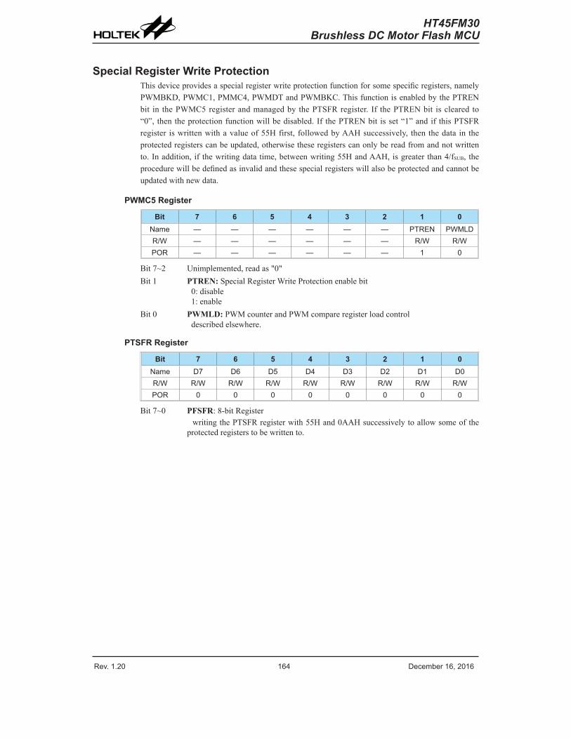
Rev. 1.20 1�4 De�e��e� 1�� 201� Rev. 1.20 1�5 De�e��e� 1�� 201�
HT45FM30Brushless DC Motor Flash MCU
Special Register Write ProtectionThisdeviceprovidesaspecialregisterwriteprotectionfunctionforsomespecificregisters,namelyPWMBKD,PWMC1,PMMC4,PWMDTandPWMBKC.ThisfunctionisenabledbythePTRENbit in thePWMC5registerandmanagedbythePTSFRregister. If thePTRENbit isclearedto“0”, thentheprotectionfunctionwillbedisabled.If thePTRENbit isset“1”andif thisPTSFRregister iswrittenwithavalueof55Hfirst, followedbyAAHsuccessively, thenthedata in theprotectedregisterscanbeupdated,otherwisetheseregisterscanonlybereadfromandnotwrittento.Inaddition,if thewritingdatatime,betweenwriting55HandAAH,isgreaterthan4/fSUB, theprocedurewillbedefinedasinvalidandthesespecialregisterswillalsobeprotectedandcannotbeupdatedwithnewdata.
PWMC5 Register
Bit 7 6 5 4 3 2 1 0Na�e — — — — — — PTREN PWMLDR/W — — — — — — R/W R/WPOR — — — — — — 1 0
Bit7~2 Unimplemented,readas"0"Bit1 PTREN:SpecialRegisterWriteProtectionenablebit
0:disable1:enable
Bit0 PWMLD:PWMcounterandPWMcompareregisterloadcontroldescribedelsewhere.
PTSFR Register
Bit 7 6 5 4 3 2 1 0Na�e D7 D� D5 D4 D3 D2 D1 D0R/W R/W R/W R/W R/W R/W R/W R/W R/WPOR 0 0 0 0 0 0 0 0
Bit7~0 PFSFR:8-bitRegisterwritingthePTSFRregisterwith55Hand0AAHsuccessivelytoallowsomeoftheprotectedregisterstobewrittento.
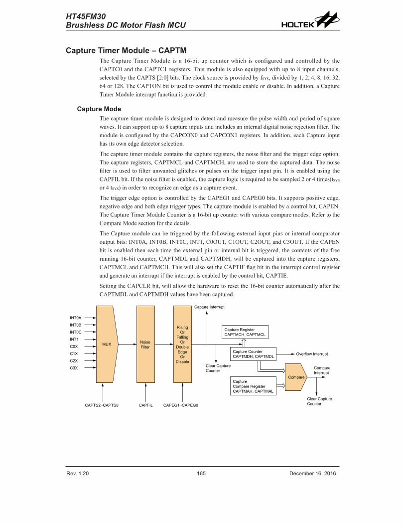
Rev. 1.20 1�4 De�e��e� 1�� 201� Rev. 1.20 1�5 De�e��e� 1�� 201�
HT45FM30Brushless DC Motor Flash MCU
Capture Timer Module – CAPTMTheCaptureTimerModule isa16-bitupcounterwhich isconfiguredandcontrolledby theCAPTC0andtheCAPTC1registers.Thismodule isalsoequippedwithupto8 inputchannels,selectedbytheCAPTS[2:0]bits.TheclocksourceisprovidedbyfSYS,dividedby1,2,4,8,16,32,64or128.TheCAPTONbitisusedtocontrolthemoduleenableordisable.Inaddition,aCaptureTimerModuleinterruptfunctionisprovided.
Capture ModeThecapturetimermoduleisdesignedtodetectandmeasurethepulsewidthandperiodofsquarewaves.Itcansupportupto8captureinputsandincludesaninternaldigitalnoiserejectionfilter.ThemoduleisconfiguredbytheCAPCON0andCAPCON1registers.Inaddition,eachCaptureinputhasitsownedgedetectorselection.
Thecapturetimermodulecontainsthecaptureregisters,thenoisefilterandthetriggeredgeoption.Thecaptureregisters,CAPTMCLandCAPTMCH,areusedtostorethecaptureddata.Thenoisefilter isusedtofilterunwantedglitchesorpulsesonthetriggerinputpin.It isenabledusingtheCAPFILbit.Ifthenoisefilterisenabled,thecapturelogicisrequiredtobesampled2or4times(tSYSor4tSYS)inordertorecognizeanedgeasacaptureevent.
ThetriggeredgeoptioniscontrolledbytheCAPEG1andCAPEG0bits.Itsupportspositiveedge,negativeedgeandbothedgetriggertypes.Thecapturemoduleisenabledbyacontrolbit,CAPEN.TheCaptureTimerModuleCounterisa16-bitupcounterwithvariouscomparemodes.RefertotheCompareModesectionforthedetails.
TheCapturemodulecanbetriggeredbythefollowingexternalinputpinsorinternalcomparatoroutputbits:INT0A,INT0B,INT0C,INT1,C0OUT,C1OUT,C2OUT,andC3OUT.IftheCAPENbit isenabledtheneachtimetheexternalpinor internalbit is triggered, thecontentsof thefreerunning16-bitcounter,CAPTMDLandCAPTMDH,willbecapturedinto thecaptureregisters,CAPTMCLandCAPTMCH.ThiswillalsosettheCAPTIFflagbitintheinterruptcontrolregisterandgenerateaninterruptiftheinterruptisenabledbythecontrolbit,CAPTIE.
SettingtheCAPCLRbit,willallowthehardwaretoresetthe16-bitcounterautomaticallyaftertheCAPTMDLandCAPTMDHvalueshavebeencaptured.
INT0A
MUX
CAPTS2~CAPTS0 CAPFIL CAPEG1~CAPEG0
Clear CaptureCounter
CaptureCompare RegisterCAPTMAH, CAPTMAL
Capture CounterCAPTMDH, CAPTMDL
Capture RegisterCAPTMCH, CAPTMCL
Overflow Interrupt
CompareInterrupt
Compare
Clear CaptureCounter
Capture Interrupt
NoiseFilter
RisingOr
FallingOr
DoubleEdge
OrDisable
INT0B
INT0C
INT1
C0X
C1X
C2X
C3X
Rev. 1.20 1�� De�e��e� 1�� 201� Rev. 1.20 1�7 De�e��e� 1�� 201�
HT45FM30Brushless DC Motor Flash MCU
Compare ModeTheCAPTMcanbeconfiguredtobeinaComparemode.CAPTMALandCAPTMAHareusedasthecompareregisters.WhentheCAPTMcountercountsuptomatchwiththeCAPTMALandCAPTMAHvalues,theCAPTMFbitwillbesetwhichwillthengenerateaninterruptrequest.
SettingtheCAPTCLRbittohighwillallowthehardwaretoresettheCAPTMcounterautomaticallyafteracomparematchoccurs.
Capture Timer Module InterruptTheCaptureTimerModulehasthreeinterrupts,CaptureInterrupt,ComparematchinterruptandCapturecounteroverflowinterrupt.ThesethreeInterruptsrequestswilltakeplacewhentheCaptureTimerModulerequestflags,CAPTIF,CAPTMF,andCAPTOFareset.Toallowtheprogramtobranchto itsrespectiveinterruptvectoraddress, theglobal interruptenablebit,EMI,respectiveCaptureTimerModuleInterruptenablebit,andrelevantInterruptenablebit,CAPTIE,CAPTMEandCAPTOE,mustfirstbeset.Whentheinterruptisenabled,thestackisnotfull,whenacapture,comparematchorcapturecounteroverflowoccurs,asubroutinecalltotherelevantinterruptvectorlocation,willtakeplace.RefertotheInterruptsectionfordetails.
Capture Timer Register List
Name Bit7 Bit6 Bit5 Bit4 Bit3 Bit2 Bit1 Bit0CAPTC0 CAPTPAU CAPTCK2 CAPTCK1 CAPTCK0 CAPTON CAPTS2 CAPTS1 CAPTS0CAPTC1 CAPEG1 CAPEG0 CAPEN CAPNFT CAPNFS CAPFIL CAPCLR CAPTCLR
CAPTMDL D7 D� D5 D4 D3 D2 D1 D0CAPTMDH D15 D14 D13 D12 D11 D10 D9 D8CAPTMAL D7 D� D5 D4 D3 D2 D1 D0CAPTMAH D15 D14 D13 D12 D11 D10 D9 D8CAPTMCL D7 D� D5 D4 D3 D2 D1 D0CAPTMCH D15 D14 D13 D12 D11 D10 D9 D8
Rev. 1.20 1�� De�e��e� 1�� 201� Rev. 1.20 1�7 De�e��e� 1�� 201�
HT45FM30Brushless DC Motor Flash MCU
CAPTC0 Register
Bit 7 6 5 4 3 2 1 0Na�e CAPTPAU CAPTCK2 CAPTCK1 CAPTCK0 CAPTON CAPTS2 CAPTS1 CAPTS0R/W R/W R/W R/W R/W R/W R/W R/W R/WPOR 0 0 0 0 0 0 0 0
Bit7 CAPTPAU:CAPTMCounterPauseControl0:run1:pauseThecountercanbepausedbysetting thisbit tohigh.Clearingthebit tozerowillrestorenormalcounteroperation.When in thePausecondition, theCAPTMwillremainpoweredupandcontinuetoconsumepower.Thecounterwillretainitsresidualvaluewhenthisbitissettohighandresumecountingfromthisvaluewhenthisbitissettolow.
Bit6~4 CAPTCK2~CAPTCK0:SelectCAPTMCounterclock000:fSYS/1001:fSYS/2010:fSYS/4011:fSYS/8100:fSYS/16101:fSYS/32110:fSYS/64111:fSYS/128ThesethreebitsareusedtoselecttheclocksourcefortheCAPTM.TheclocksourcefSYSisthesystemclock.
Bit3 CAPTON:CAPTMCounterOn/OffControl0:off1:onThisbitcontrols theoverallon/off functionof theCAPTM.Setting thebithighwillenable thecounterandclearingthebitwilldisable theCAPTM.Clearingthisbit tozerowillstopthecounterfromcountingandturnoff theCAPTM.Whenthebitchangesstatefromlowtohigh, the internalcountervaluewillbereset tozero,howeverwhenthebitchangesfromhightolow, theinternalcounterwillretainitsresidualvalue.
Bit0~2 CAPTS2~CAPTS0:SelectCAPTMcaptureinput000:INT0A001:INT0B010:INT0C011:INT1100:C0OUT101:C1OUT110:C2OUT111:C3OUTThesethreebitsareusedtoselectthecaptureinputfortheCAPTM.
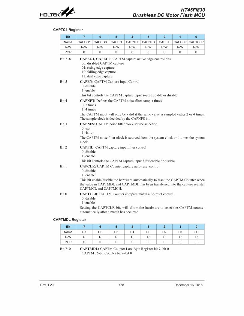
Rev. 1.20 1�8 De�e��e� 1�� 201� Rev. 1.20 1�9 De�e��e� 1�� 201�
HT45FM30Brushless DC Motor Flash MCU
CAPTC1 Register
Bit 7 6 5 4 3 2 1 0Na�e CAPEG1 CAPEG0 CAPEN CAPNFT CAPNFS CAPFIL CAPCLR CAPTCLRR/W R/W R/W R/W R/W R/W R/W R/W R/WPOR 0 0 0 0 0 0 0 0
Bit7~6 CAPEG1, CAPEG0:CAPTMcaptureactiveedgecontrolbits00:disabledCAPTMcapture01:risingedgecapture10:fallingedgecapture11:dualedgecapture
Bit5 CAPEN:CAPTMCaptureInputControl0:disable1:enableThisbitcontrolstheCAPTMcaptureinputsourceenableordisable.
Bit4 CAPNFT:DefinestheCAPTMnoisefiltersampletimes0:2times1:4timesTheCAPTMinputwillonlybevalidifthesamevalueissampledeither2or4times.ThesampleclockisdecidedbytheCAPNFSbit.
Bit3 CAPNFS:CAPTMnoisefilterclocksourceselection0:tSYS1:4tSYS
TheCAPTMnoisefilterclockissourcedfromthesystemclockor4timesthesystemclock.
Bit2 CAPFIL:CAPTMcaptureinputfiltercontrol0:disable1:enableThisbitcontrolstheCAPTMcaptureinputfilterenableordisable.
Bit1 CAPCLR: CAPTMCountercaptureauto-resetcontrol0:disable1:enableThisbitenable/disablethehardwareautomaticallytoresettheCAPTMCounterwhenthevalueinCAPTMDLandCAPTMDHhasbeentransferredintothecaptureregisterCAPTMCLandCAPTMCH.
Bit0 CAPTCLR: CAPTMCountercomparematchauto-resetcontrol0:disable1:enableSetting theCAPTCLRbit,willallow thehardware to reset theCAPTMcounterautomaticallyafteramatchhasoccurred.
CAPTMDL Register
Bit 7 6 5 4 3 2 1 0Na�e D7 D� D5 D4 D3 D2 D1 D0R/W R R R R R R R RPOR 0 0 0 0 0 0 0 0
Bit7~0 CAPTMDL:CAPTMCounterLowByteRegisterbit7~bit0CAPTM16-bitCounterbit7~bit0
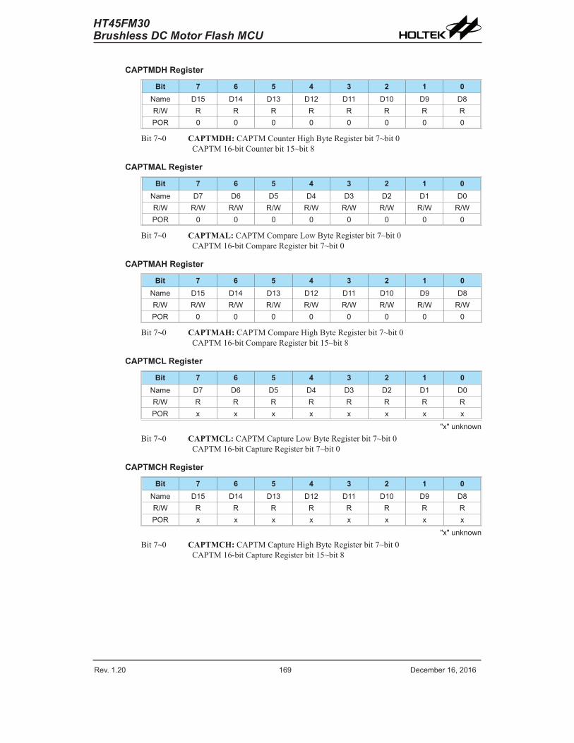
Rev. 1.20 1�8 De�e��e� 1�� 201� Rev. 1.20 1�9 De�e��e� 1�� 201�
HT45FM30Brushless DC Motor Flash MCU
CAPTMDH Register
Bit 7 6 5 4 3 2 1 0Na�e D15 D14 D13 D12 D11 D10 D9 D8R/W R R R R R R R RPOR 0 0 0 0 0 0 0 0
Bit7~0 CAPTMDH:CAPTMCounterHighByteRegisterbit7~bit0CAPTM16-bitCounterbit15~bit8
CAPTMAL Register
Bit 7 6 5 4 3 2 1 0Na�e D7 D� D5 D4 D3 D2 D1 D0R/W R/W R/W R/W R/W R/W R/W R/W R/WPOR 0 0 0 0 0 0 0 0
Bit7~0 CAPTMAL:CAPTMCompareLowByteRegisterbit7~bit0CAPTM16-bitCompareRegisterbit7~bit0
CAPTMAH Register
Bit 7 6 5 4 3 2 1 0Na�e D15 D14 D13 D12 D11 D10 D9 D8R/W R/W R/W R/W R/W R/W R/W R/W R/WPOR 0 0 0 0 0 0 0 0
Bit7~0 CAPTMAH:CAPTMCompareHighByteRegisterbit7~bit0CAPTM16-bitCompareRegisterbit15~bit8
CAPTMCL Register
Bit 7 6 5 4 3 2 1 0Na�e D7 D� D5 D4 D3 D2 D1 D0R/W R R R R R R R RPOR x x x x x x x x
"x" unknownBit7~0 CAPTMCL:CAPTMCaptureLowByteRegisterbit7~bit0
CAPTM16-bitCaptureRegisterbit7~bit0
CAPTMCH Register
Bit 7 6 5 4 3 2 1 0Na�e D15 D14 D13 D12 D11 D10 D9 D8R/W R R R R R R R RPOR x x x x x x x x
"x" unknownBit7~0 CAPTMCH:CAPTMCaptureHighByteRegisterbit7~bit0
CAPTM16-bitCaptureRegisterbit15~bit8
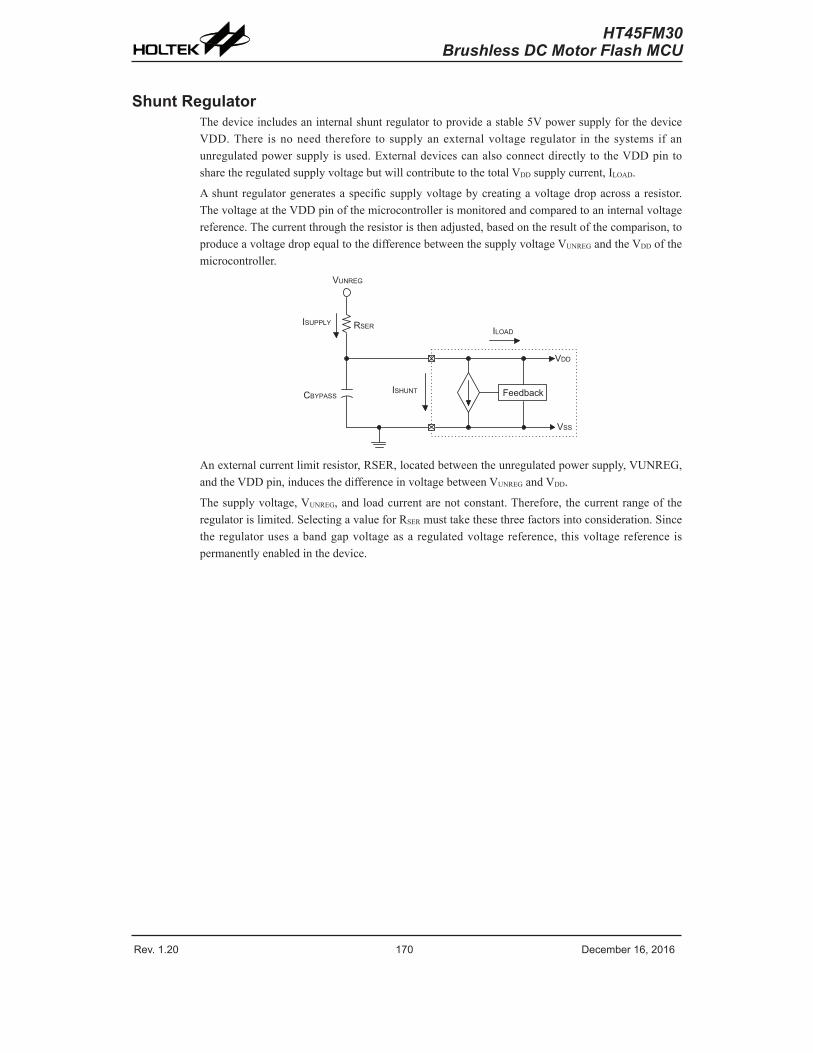
Rev. 1.20 170 De�e��e� 1�� 201� Rev. 1.20 171 De�e��e� 1�� 201�
HT45FM30Brushless DC Motor Flash MCU
Shunt RegulatorThedeviceincludesaninternalshuntregulatortoprovideastable5VpowersupplyforthedeviceVDD.There isnoneed therefore tosupplyanexternalvoltage regulator in thesystems ifanunregulatedpowersupplyisused.Externaldevicescanalsoconnectdirectlyto theVDDpintosharetheregulatedsupplyvoltagebutwillcontributetothetotalVDDsupplycurrent,ILOAD.
Ashuntregulatorgeneratesaspecificsupplyvoltagebycreatingavoltagedropacrossaresistor.ThevoltageattheVDDpinofthemicrocontrollerismonitoredandcomparedtoaninternalvoltagereference.Thecurrentthroughtheresistoristhenadjusted,basedontheresultofthecomparison,toproduceavoltagedropequaltothedifferencebetweenthesupplyvoltageVUNREGandtheVDDofthemicrocontroller.
� � � � � �
� � � � � � � � � � �
� � � � � � �� � � � � �
� � � � �
� � � � �
� � �
� � �
Anexternalcurrentlimitresistor,RSER,locatedbetweentheunregulatedpowersupply,VUNREG,andtheVDDpin,inducesthedifferenceinvoltagebetweenVUNREGandVDD.
Thesupplyvoltage,VUNREG,andloadcurrentarenotconstant.Therefore,thecurrentrangeoftheregulatorislimited.SelectingavalueforRSERmusttakethesethreefactorsintoconsideration.Sincetheregulatorusesabandgapvoltageasaregulatedvoltagereference, thisvoltagereference ispermanentlyenabledinthedevice.
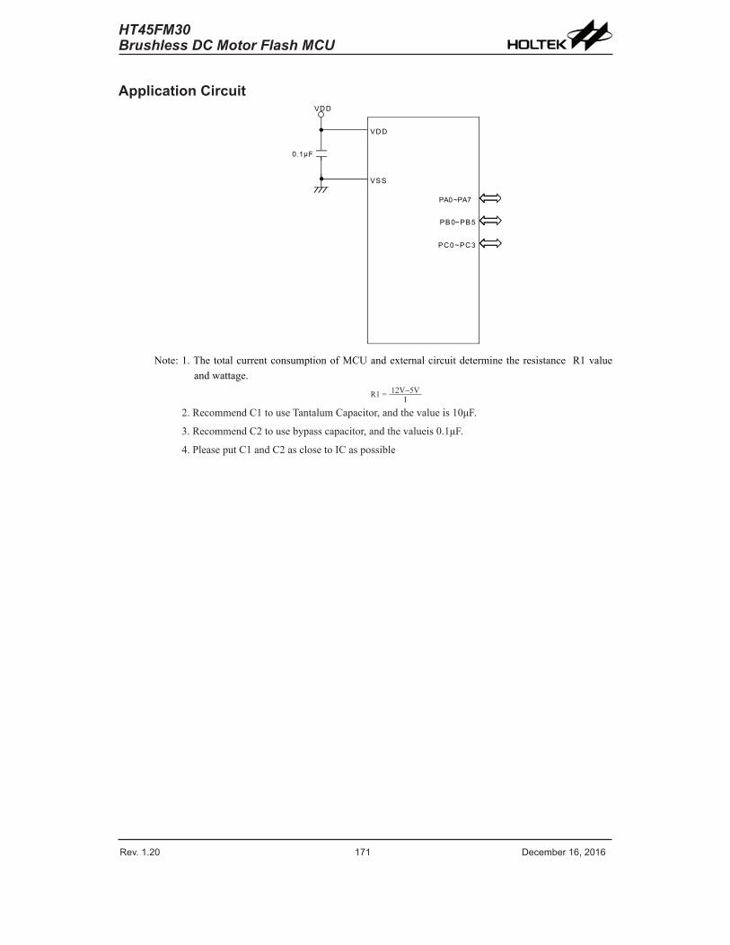
Rev. 1.20 170 De�e��e� 1�� 201� Rev. 1.20 171 De�e��e� 1�� 201�
HT45FM30Brushless DC Motor Flash MCU
Application Circuit
PA0~PA7
PB 0~PB 5
PC0~PC3
VDD
VS S
0.1µF
VDD
Note:1.ThetotalcurrentconsumptionofMCUandexternalcircuitdeterminetheresistanceR1valueandwattage.
� � � � � � � � � ��
2.RecommendC1touseTantalumCapacitor,andthevalueis10μF.
3.RecommendC2tousebypasscapacitor,andthevalueis0.1μF.
4.PleaseputC1andC2asclosetoICaspossible
Rev. 1.20 172 De�e��e� 1�� 201� Rev. 1.20 173 De�e��e� 1�� 201�
HT45FM30Brushless DC Motor Flash MCU
Instruction Set
IntroductionCentral to thesuccessfuloperationofanymicrocontroller is its instructionset,whichisasetofprograminstructioncodesthatdirectsthemicrocontrollertoperformcertainoperations.InthecaseofHoltekmicrocontrollers,acomprehensiveandflexiblesetofover60instructionsisprovidedtoenableprogrammerstoimplementtheirapplicationwiththeminimumofprogrammingoverheads.
Foreasierunderstandingofthevariousinstructioncodes, theyhavebeensubdividedintoseveralfunctionalgroupings.
Instruction TimingMostinstructionsareimplementedwithinoneinstructioncycle.Theexceptionstothisarebranch,call,or tablereadinstructionswheretwoinstructioncyclesarerequired.Oneinstructioncycleisequalto4systemclockcycles,thereforeinthecaseofan8MHzsystemoscillator,mostinstructionswouldbeimplementedwithin0.5µsandbranchorcall instructionswouldbeimplementedwithin1µs.Althoughinstructionswhichrequireonemorecycle to implementaregenerally limited totheJMP,CALL,RET,RETIandtablereadinstructions, it is important torealize thatanyotherinstructionswhichinvolvemanipulationoftheProgramCounterLowregisterorPCLwillalsotakeonemorecycletoimplement.AsinstructionswhichchangethecontentsofthePCLwill implyadirect jumptothatnewaddress,onemorecyclewillberequired.Examplesofsuchinstructionswouldbe″CLRPCL″or″MOVPCL,A″.Forthecaseofskipinstructions,itmustbenotedthatiftheresultofthecomparisoninvolvesaskipoperationthenthiswillalsotakeonemorecycle,ifnoskipisinvolvedthenonlyonecycleisrequired.
Moving and Transferring DataThe transferofdatawithin themicrocontrollerprogram isoneof themost frequentlyusedoperations.MakinguseofthreekindsofMOVinstructions,datacanbetransferredfromregisterstotheAccumulatorandvice-versaaswellasbeingabletomovespecificimmediatedatadirectlyintotheAccumulator.Oneofthemostimportantdatatransferapplicationsis toreceivedatafromtheinputportsandtransferdatatotheoutputports.
Arithmetic OperationsTheabilitytoperformcertainarithmeticoperationsanddatamanipulationisanecessaryfeatureofmostmicrocontrollerapplications.WithintheHoltekmicrocontrollerinstructionsetarearangeofaddandsubtract instructionmnemonicstoenablethenecessaryarithmetictobecarriedout.Caremustbe taken toensurecorrecthandlingofcarryandborrowdatawhenresultsexceed255foradditionandlessthan0forsubtraction.TheincrementanddecrementinstructionsINC,INCA,DECandDECAprovideasimplemeansofincreasingordecreasingbyavalueofoneofthevaluesinthedestinationspecified.
Rev. 1.20 172 De�e��e� 1�� 201� Rev. 1.20 173 De�e��e� 1�� 201�
HT45FM30Brushless DC Motor Flash MCU
Logical and Rotate OperationsThestandardlogicaloperationssuchasAND,OR,XORandCPLallhavetheirowninstructionwithintheHoltekmicrocontroller instructionset.Aswiththecaseofmost instructionsinvolvingdatamanipulation, datamust pass through theAccumulatorwhichmay involve additionalprogrammingsteps. Inall logicaldataoperations, thezero flagmaybeset if the resultof theoperationiszero.AnotherformoflogicaldatamanipulationcomesfromtherotateinstructionssuchasRR,RL,RRCandRLCwhichprovideasimplemeansofrotatingonebitrightorleft.Differentrotateinstructionsexistdependingonprogramrequirements.Rotateinstructionsareusefulforserialportprogrammingapplicationswheredatacanberotatedfromaninternalregister intotheCarrybitfromwhereitcanbeexaminedandthenecessaryserialbitsethighorlow.Anotherapplicationwhererotatedataoperationsareusedistoimplementmultiplicationanddivisioncalculations.
Branches and Control TransferProgrambranchingtakestheformofeitherjumpstospecifiedlocationsusingtheJMPinstructionortoasubroutineusingtheCALLinstruction.Theydifferinthesensethatinthecaseofasubroutinecall, theprogrammustreturntotheinstructionimmediatelywhenthesubroutinehasbeencarriedout.ThisisdonebyplacingareturninstructionRETinthesubroutinewhichwillcausetheprogramtojumpbacktotheaddressrightaftertheCALLinstruction.InthecaseofaJMPinstruction,theprogramsimplyjumpstothedesiredlocation.Thereisnorequirementtojumpbacktotheoriginaljumpingoffpointas in thecaseof theCALLinstruction.Onespecialandextremelyusefulsetofbranch instructionsare theconditionalbranches.Hereadecision is firstmaderegarding theconditionofacertaindatamemoryorindividualbits.Dependingupontheconditions,theprogramwillcontinuewiththenextinstructionorskipoveritandjumptothefollowinginstruction.Theseinstructionsarethekeytodecisionmakingandbranchingwithintheprogramperhapsdeterminedbytheconditionofcertaininputswitchesorbytheconditionofinternaldatabits.
Bit OperationsTheabilitytoprovidesinglebitoperationsonDataMemoryisanextremelyflexiblefeatureofallHoltekmicrocontrollers.Thisfeature isespeciallyusefulforoutputportbitprogrammingwhereindividualbitsorportpinscanbedirectlysethighorlowusingeitherthe″SET[m].i″or″CLR[m].i″instructionsrespectively.Thefeatureremovestheneedforprogrammerstofirstreadthe8-bitoutputport,manipulatetheinputdatatoensurethatotherbitsarenotchangedandthenoutputtheportwiththecorrectnewdata.Thisread-modify-writeprocessistakencareofautomaticallywhenthesebitoperationinstructionsareused.
Table Read OperationsDatastorage isnormally implementedbyusing registers.However,whenworkingwith largeamountsoffixeddata, thevolumeinvolvedoftenmakesit inconvenienttostorethefixeddataintheDataMemory.Toovercomethisproblem,HoltekmicrocontrollersallowanareaofProgramMemorytobesetupasatablewheredatacanbedirectlystored.Asetofeasytouseinstructionsprovides themeansbywhich this fixeddatacanbereferencedandretrievedfromtheProgramMemory.
Other OperationsInaddition to theabovefunctional instructions,a rangeofother instructionsalsoexistsuchasthe″HALT″instructionforPower-downoperationsand instructions tocontrol theoperationoftheWatchdogTimerfor reliableprogramoperationsunderextremeelectricorelectromagneticenvironments.Fortheirrelevantoperations,refertothefunctionalrelatedsections.
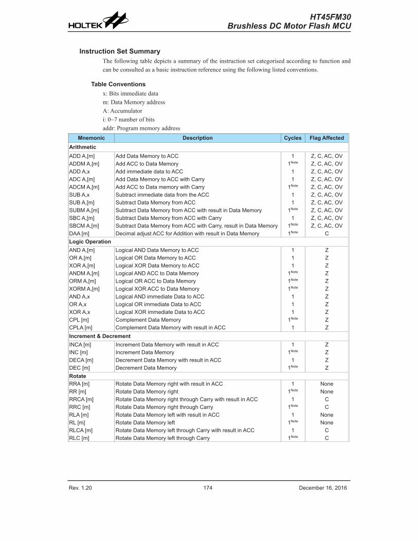
Rev. 1.20 174 De�e��e� 1�� 201� Rev. 1.20 175 De�e��e� 1�� 201�
HT45FM30Brushless DC Motor Flash MCU
Instruction Set SummaryThefollowingtabledepictsasummaryoftheinstructionsetcategorisedaccordingtofunctionandcanbeconsultedasabasicinstructionreferenceusingthefollowinglistedconventions.
Table Conventionsx:Bitsimmediatedatam:DataMemoryaddressA:Accumulatori:0~7numberofbitsaddr:Programmemoryaddress
Mnemonic Description Cycles Flag AffectedArithmeticADD A�[�] Add Data Me�o�y to ACC 1 Z� C� AC� OVADDM A�[�] Add ACC to Data Me�o�y 1Note Z� C� AC� OVADD A�x Add i��ediate data to ACC 1 Z� C� AC� OVADC A�[�] Add Data Me�o�y to ACC with Ca��y 1 Z� C� AC� OVADCM A�[�] Add ACC to Data �e�o�y with Ca��y 1Note Z� C� AC� OVSUB A�x Su�t�a�t i��ediate data f�o� the ACC 1 Z� C� AC� OVSUB A�[�] Su�t�a�t Data Me�o�y f�o� ACC 1 Z� C� AC� OVSUBM A�[�] Su�t�a�t Data Me�o�y f�o� ACC with �esult in Data Me�o�y 1Note Z� C� AC� OVSBC A�[�] Su�t�a�t Data Me�o�y f�o� ACC with Ca��y 1 Z� C� AC� OVSBCM A�[�] Su�t�a�t Data Me�o�y f�o� ACC with Ca��y� �esult in Data Me�o�y 1Note Z� C� AC� OVDAA [�] De�i�al adjust ACC fo� Addition with �esult in Data Me�o�y 1Note CLogic OperationAND A�[�] Logi�al AND Data Me�o�y to ACC 1 ZOR A�[�] Logi�al OR Data Me�o�y to ACC 1 ZXOR A�[�] Logi�al XOR Data Me�o�y to ACC 1 ZANDM A�[�] Logi�al AND ACC to Data Me�o�y 1Note ZORM A�[�] Logi�al OR ACC to Data Me�o�y 1Note ZXORM A�[�] Logi�al XOR ACC to Data Me�o�y 1Note ZAND A�x Logi�al AND i��ediate Data to ACC 1 ZOR A�x Logi�al OR i��ediate Data to ACC 1 ZXOR A�x Logi�al XOR i��ediate Data to ACC 1 ZCPL [�] Co�ple�ent Data Me�o�y 1Note ZCPLA [�] Co�ple�ent Data Me�o�y with �esult in ACC 1 ZIncrement & DecrementINCA [�] In��e�ent Data Me�o�y with �esult in ACC 1 ZINC [�] In��e�ent Data Me�o�y 1Note ZDECA [�] De��e�ent Data Me�o�y with �esult in ACC 1 ZDEC [�] De��e�ent Data Me�o�y 1Note ZRotateRRA [�] Rotate Data Me�o�y �ight with �esult in ACC 1 NoneRR [�] Rotate Data Me�o�y �ight 1Note NoneRRCA [�] Rotate Data Me�o�y �ight th�ough Ca��y with �esult in ACC 1 CRRC [�] Rotate Data Me�o�y �ight th�ough Ca��y 1Note CRLA [�] Rotate Data Me�o�y left with �esult in ACC 1 NoneRL [�] Rotate Data Me�o�y left 1Note NoneRLCA [�] Rotate Data Me�o�y left th�ough Ca��y with �esult in ACC 1 CRLC [�] Rotate Data Me�o�y left th�ough Ca��y 1Note C
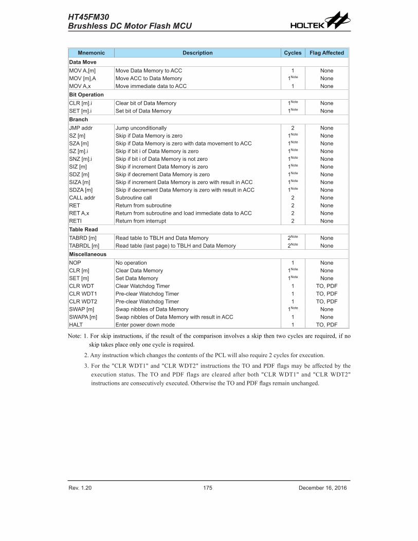
Rev. 1.20 174 De�e��e� 1�� 201� Rev. 1.20 175 De�e��e� 1�� 201�
HT45FM30Brushless DC Motor Flash MCU
Mnemonic Description Cycles Flag AffectedData MoveMOV A�[�] Move Data Me�o�y to ACC 1 NoneMOV [�]�A Move ACC to Data Me�o�y 1Note NoneMOV A�x Move i��ediate data to ACC 1 NoneBit OperationCLR [�].i Clea� �it of Data Me�o�y 1Note NoneSET [�].i Set �it of Data Me�o�y 1Note NoneBranchJMP add� Ju�p un�onditionally 2 NoneSZ [�] Skip if Data Me�o�y is ze�o 1Note NoneSZA [�] Skip if Data Me�o�y is ze�o with data �ove�ent to ACC 1Note NoneSZ [�].i Skip if �it i of Data Me�o�y is ze�o 1Note NoneSNZ [�].i Skip if �it i of Data Me�o�y is not ze�o 1Note NoneSIZ [�] Skip if in��e�ent Data Me�o�y is ze�o 1Note NoneSDZ [�] Skip if de��e�ent Data Me�o�y is ze�o 1Note NoneSIZA [�] Skip if in��e�ent Data Me�o�y is ze�o with �esult in ACC 1Note NoneSDZA [�] Skip if de��e�ent Data Me�o�y is ze�o with �esult in ACC 1Note NoneCALL add� Su��outine �all 2 NoneRET Retu�n f�o� su��outine 2 NoneRET A�x Retu�n f�o� su��outine and load i��ediate data to ACC 2 NoneRETI Retu�n f�o� inte��upt 2 NoneTable ReadTABRD [�] Read ta�le to TBLH and Data Me�o�y 2Note NoneTABRDL [�] Read ta�le (last page) to TBLH and Data Me�o�y 2Note NoneMiscellaneousNOP No ope�ation 1 NoneCLR [�] Clea� Data Me�o�y 1Note NoneSET [�] Set Data Me�o�y 1Note NoneCLR WDT Clea� Wat�hdog Ti�e� 1 TO� PDFCLR WDT1 P�e-�lea� Wat�hdog Ti�e� 1 TO� PDFCLR WDT2 P�e-�lea� Wat�hdog Ti�e� 1 TO� PDFSWAP [�] Swap ni��les of Data Me�o�y 1Note NoneSWAPA [�] Swap ni��les of Data Me�o�y with �esult in ACC 1 NoneHALT Ente� powe� down �ode 1 TO� PDF
Note:1.Forskipinstructions,iftheresultofthecomparisoninvolvesaskipthentwocyclesarerequired,ifnoskiptakesplaceonlyonecycleisrequired.
2.AnyinstructionwhichchangesthecontentsofthePCLwillalsorequire2cyclesforexecution.
3.For the"CLRWDT1"and"CLRWDT2"instructions theTOandPDFflagsmaybeaffectedbytheexecution status.TheTOandPDF flagsareclearedafterboth "CLRWDT1"and"CLRWDT2"instructionsareconsecutivelyexecuted.OtherwisetheTOandPDFflagsremainunchanged.
Rev. 1.20 17� De�e��e� 1�� 201� Rev. 1.20 177 De�e��e� 1�� 201�
HT45FM30Brushless DC Motor Flash MCU
Instruction Definition
ADC A,[m] AddDataMemorytoACCwithCarryDescription ThecontentsofthespecifiedDataMemory,Accumulatorandthecarryflagareadded. TheresultisstoredintheAccumulator.Operation ACC←ACC+[m]+CAffectedflag(s) OV,Z,AC,C
ADCM A,[m] AddACCtoDataMemorywithCarryDescription ThecontentsofthespecifiedDataMemory,Accumulatorandthecarryflagareadded. TheresultisstoredinthespecifiedDataMemory.Operation [m]←ACC+[m]+CAffectedflag(s) OV,Z,AC,C
ADD A,[m] AddDataMemorytoACCDescription ThecontentsofthespecifiedDataMemoryandtheAccumulatorareadded. TheresultisstoredintheAccumulator.Operation ACC←ACC+[m]Affectedflag(s) OV,Z,AC,C
ADD A,x AddimmediatedatatoACCDescription ThecontentsoftheAccumulatorandthespecifiedimmediatedataareadded. TheresultisstoredintheAccumulator.Operation ACC←ACC+xAffectedflag(s) OV,Z,AC,C
ADDM A,[m] AddACCtoDataMemoryDescription ThecontentsofthespecifiedDataMemoryandtheAccumulatorareadded. TheresultisstoredinthespecifiedDataMemory.Operation [m]←ACC+[m]Affectedflag(s) OV,Z,AC,C
AND A,[m] LogicalANDDataMemorytoACCDescription DataintheAccumulatorandthespecifiedDataMemoryperformabitwiselogicalAND operation.TheresultisstoredintheAccumulator.Operation ACC←ACC″AND″[m]Affectedflag(s) Z
AND A,x LogicalANDimmediatedatatoACCDescription DataintheAccumulatorandthespecifiedimmediatedataperformabitwiselogicalAND operation.TheresultisstoredintheAccumulator.Operation ACC←ACC″AND″xAffectedflag(s) Z
ANDM A,[m] LogicalANDACCtoDataMemoryDescription DatainthespecifiedDataMemoryandtheAccumulatorperformabitwiselogicalAND operation.TheresultisstoredintheDataMemory.Operation [m]←ACC″AND″[m]Affectedflag(s) Z
Rev. 1.20 17� De�e��e� 1�� 201� Rev. 1.20 177 De�e��e� 1�� 201�
HT45FM30Brushless DC Motor Flash MCU
CALL addr SubroutinecallDescription Unconditionallycallsasubroutineatthespecifiedaddress.TheProgramCounterthen incrementsby1toobtaintheaddressofthenextinstructionwhichisthenpushedontothe stack.Thespecifiedaddressisthenloadedandtheprogramcontinuesexecutionfromthis newaddress.Asthisinstructionrequiresanadditionaloperation,itisatwocycleinstruction.Operation Stack←ProgramCounter+1 ProgramCounter←addrAffectedflag(s) None
CLR [m] ClearDataMemoryDescription EachbitofthespecifiedDataMemoryisclearedto0.Operation [m]←00HAffectedflag(s) None
CLR [m].i ClearbitofDataMemoryDescription BitiofthespecifiedDataMemoryisclearedto0.Operation [m].i←0Affectedflag(s) None
CLR WDT ClearWatchdogTimerDescription TheTO,PDFflagsandtheWDTareallcleared.Operation WDTcleared TO←0 PDF←0Affectedflag(s) TO,PDF
CPL [m] ComplementDataMemoryDescription EachbitofthespecifiedDataMemoryislogicallycomplemented(1′scomplement).Bitswhich previouslycontaineda1arechangedto0andviceversa.Operation [m]←[m]Affectedflag(s) Z
Rev. 1.20 178 De�e��e� 1�� 201� Rev. 1.20 179 De�e��e� 1�� 201�
HT45FM30Brushless DC Motor Flash MCU
CPLA [m] ComplementDataMemorywithresultinACCDescription EachbitofthespecifiedDataMemoryislogicallycomplemented(1′scomplement).Bitswhich previouslycontaineda1arechangedto0andviceversa.Thecomplementedresultisstoredin theAccumulatorandthecontentsoftheDataMemoryremainunchanged.Operation ACC←[m]Affectedflag(s) Z
DAA [m] Decimal-AdjustACCforadditionwithresultinDataMemoryDescription ConvertthecontentsoftheAccumulatorvaluetoaBCD(BinaryCodedDecimal)value resultingfromthepreviousadditionoftwoBCDvariables.Ifthelownibbleisgreaterthan9 orifACflagisset,thenavalueof6willbeaddedtothelownibble.Otherwisethelownibble remainsunchanged.Ifthehighnibbleisgreaterthan9oriftheCflagisset,thenavalueof6 willbeaddedtothehighnibble.Essentially,thedecimalconversionisperformedbyadding 00H,06H,60Hor66HdependingontheAccumulatorandflagconditions.OnlytheCflag maybeaffectedbythisinstructionwhichindicatesthatiftheoriginalBCDsumisgreaterthan 100,itallowsmultipleprecisiondecimaladdition.Operation [m]←ACC+00Hor [m]←ACC+06Hor [m]←ACC+60Hor [m]←ACC+66HAffectedflag(s) C
DEC [m] DecrementDataMemoryDescription DatainthespecifiedDataMemoryisdecrementedby1.Operation [m]←[m]−1Affectedflag(s) Z
DECA[m] DecrementDataMemorywithresultinACCDescription DatainthespecifiedDataMemoryisdecrementedby1.Theresultisstoredinthe Accumulator.ThecontentsoftheDataMemoryremainunchanged.Operation ACC←[m]−1Affectedflag(s) Z
HALT EnterpowerdownmodeDescription Thisinstructionstopstheprogramexecutionandturnsoffthesystemclock.Thecontentsof theDataMemoryandregistersareretained.TheWDTandprescalerarecleared.Thepower downflagPDFissetandtheWDTtime-outflagTOiscleared.Operation TO←0 PDF←1Affectedflag(s) TO,PDF
INC [m] IncrementDataMemoryDescription DatainthespecifiedDataMemoryisincrementedby1.Operation [m]←[m]+1Affectedflag(s) Z
INCA [m] IncrementDataMemorywithresultinACCDescription DatainthespecifiedDataMemoryisincrementedby1.TheresultisstoredintheAccumulator. ThecontentsoftheDataMemoryremainunchanged.Operation ACC←[m]+1Affectedflag(s) Z
Rev. 1.20 178 De�e��e� 1�� 201� Rev. 1.20 179 De�e��e� 1�� 201�
HT45FM30Brushless DC Motor Flash MCU
JMP addr JumpunconditionallyDescription ThecontentsoftheProgramCounterarereplacedwiththespecifiedaddress.Program executionthencontinuesfromthisnewaddress.Asthisrequirestheinsertionofadummy instructionwhilethenewaddressisloaded,itisatwocycleinstruction.Operation ProgramCounter←addrAffectedflag(s) None
MOV A,[m] MoveDataMemorytoACCDescription ThecontentsofthespecifiedDataMemoryarecopiedtotheAccumulator.Operation ACC←[m]Affectedflag(s) None
MOV A,x MoveimmediatedatatoACCDescription TheimmediatedataspecifiedisloadedintotheAccumulator.Operation ACC←xAffectedflag(s) None
MOV [m],A MoveACCtoDataMemoryDescription ThecontentsoftheAccumulatorarecopiedtothespecifiedDataMemory.Operation [m]←ACCAffectedflag(s) None
NOP NooperationDescription Nooperationisperformed.Executioncontinueswiththenextinstruction.Operation NooperationAffectedflag(s) None
OR A,[m] LogicalORDataMemorytoACCDescription DataintheAccumulatorandthespecifiedDataMemoryperformabitwise logicalORoperation.TheresultisstoredintheAccumulator.Operation ACC←ACC″OR″[m]Affectedflag(s) Z
OR A,x LogicalORimmediatedatatoACCDescription DataintheAccumulatorandthespecifiedimmediatedataperformabitwiselogicalOR operation.TheresultisstoredintheAccumulator.Operation ACC←ACC″OR″xAffectedflag(s) Z
ORM A,[m] LogicalORACCtoDataMemoryDescription DatainthespecifiedDataMemoryandtheAccumulatorperformabitwiselogicalOR operation.TheresultisstoredintheDataMemory.Operation [m]←ACC″OR″[m]Affectedflag(s) Z
RET ReturnfromsubroutineDescription TheProgramCounterisrestoredfromthestack.Programexecutioncontinuesattherestored address.Operation ProgramCounter←StackAffectedflag(s) None
Rev. 1.20 180 De�e��e� 1�� 201� Rev. 1.20 181 De�e��e� 1�� 201�
HT45FM30Brushless DC Motor Flash MCU
RET A,x ReturnfromsubroutineandloadimmediatedatatoACCDescription TheProgramCounterisrestoredfromthestackandtheAccumulatorloadedwiththespecified immediatedata.Programexecutioncontinuesattherestoredaddress.Operation ProgramCounter←Stack ACC←xAffectedflag(s) None
RETI ReturnfrominterruptDescription TheProgramCounterisrestoredfromthestackandtheinterruptsarere-enabledbysettingthe EMIbit.EMIisthemasterinterruptglobalenablebit.Ifaninterruptwaspendingwhenthe RETIinstructionisexecuted,thependingInterruptroutinewillbeprocessedbeforereturning tothemainprogram.Operation ProgramCounter←Stack EMI←1Affectedflag(s) None
RL [m] RotateDataMemoryleftDescription ThecontentsofthespecifiedDataMemoryarerotatedleftby1bitwithbit7rotatedintobit0.Operation [m].(i+1)←[m].i;(i=0~6) [m].0←[m].7Affectedflag(s) None
RLA [m] RotateDataMemoryleftwithresultinACCDescription ThecontentsofthespecifiedDataMemoryarerotatedleftby1bitwithbit7rotatedintobit0. TherotatedresultisstoredintheAccumulatorandthecontentsoftheDataMemoryremain unchanged.Operation ACC.(i+1)←[m].i;(i=0~6) ACC.0←[m].7Affectedflag(s) None
RLC [m] RotateDataMemoryleftthroughCarryDescription ThecontentsofthespecifiedDataMemoryandthecarryflagarerotatedleftby1bit.Bit7 replacestheCarrybitandtheoriginalcarryflagisrotatedintobit0.Operation [m].(i+1)←[m].i;(i=0~6) [m].0←C C←[m].7Affectedflag(s) C
RLCA [m] RotateDataMemoryleftthroughCarrywithresultinACCDescription DatainthespecifiedDataMemoryandthecarryflagarerotatedleftby1bit.Bit7replacesthe Carrybitandtheoriginalcarryflagisrotatedintothebit0.Therotatedresultisstoredinthe AccumulatorandthecontentsoftheDataMemoryremainunchanged.Operation ACC.(i+1)←[m].i;(i=0~6) ACC.0←C C←[m].7Affectedflag(s) C
RR [m] RotateDataMemoryrightDescription ThecontentsofthespecifiedDataMemoryarerotatedrightby1bitwithbit0rotatedintobit7.Operation [m].i←[m].(i+1);(i=0~6) [m].7←[m].0Affectedflag(s) None
Rev. 1.20 180 De�e��e� 1�� 201� Rev. 1.20 181 De�e��e� 1�� 201�
HT45FM30Brushless DC Motor Flash MCU
RRA [m] RotateDataMemoryrightwithresultinACCDescription DatainthespecifiedDataMemoryandthecarryflagarerotatedrightby1bitwithbit0 rotatedintobit7.TherotatedresultisstoredintheAccumulatorandthecontentsofthe DataMemoryremainunchanged.Operation ACC.i←[m].(i+1);(i=0~6) ACC.7←[m].0Affectedflag(s) None
RRC [m] RotateDataMemoryrightthroughCarryDescription ThecontentsofthespecifiedDataMemoryandthecarryflagarerotatedrightby1bit.Bit0 replacestheCarrybitandtheoriginalcarryflagisrotatedintobit7.Operation [m].i←[m].(i+1);(i=0~6) [m].7←C C←[m].0Affectedflag(s) C
RRCA [m] RotateDataMemoryrightthroughCarrywithresultinACCDescription DatainthespecifiedDataMemoryandthecarryflagarerotatedrightby1bit.Bit0replaces theCarrybitandtheoriginalcarryflagisrotatedintobit7.Therotatedresultisstoredinthe AccumulatorandthecontentsoftheDataMemoryremainunchanged.Operation ACC.i←[m].(i+1);(i=0~6) ACC.7←C C←[m].0Affectedflag(s) C
SBC A,[m] SubtractDataMemoryfromACCwithCarryDescription ThecontentsofthespecifiedDataMemoryandthecomplementofthecarryflagare subtractedfromtheAccumulator.TheresultisstoredintheAccumulator.Notethatifthe resultofsubtractionisnegative,theCflagwillbeclearedto0,otherwiseiftheresultis positiveorzero,theCflagwillbesetto1.Operation ACC←ACC−[m]−CAffectedflag(s) OV,Z,AC,C
SBCM A,[m] SubtractDataMemoryfromACCwithCarryandresultinDataMemoryDescription ThecontentsofthespecifiedDataMemoryandthecomplementofthecarryflagare subtractedfromtheAccumulator.TheresultisstoredintheDataMemory.Notethatifthe resultofsubtractionisnegative,theCflagwillbeclearedto0,otherwiseiftheresultis positiveorzero,theCflagwillbesetto1.Operation [m]←ACC−[m]−CAffectedflag(s) OV,Z,AC,C
SDZ [m] SkipifdecrementDataMemoryis0Description ThecontentsofthespecifiedDataMemoryarefirstdecrementedby1.Iftheresultis0the followinginstructionisskipped.Asthisrequirestheinsertionofadummyinstructionwhile thenextinstructionisfetched,itisatwocycleinstruction.Iftheresultisnot0theprogram proceedswiththefollowinginstruction.Operation [m]←[m]−1 Skipif[m]=0Affectedflag(s) None
Rev. 1.20 182 De�e��e� 1�� 201� Rev. 1.20 183 De�e��e� 1�� 201�
HT45FM30Brushless DC Motor Flash MCU
SDZA [m] SkipifdecrementDataMemoryiszerowithresultinACCDescription ThecontentsofthespecifiedDataMemoryarefirstdecrementedby1.Iftheresultis0,the followinginstructionisskipped.TheresultisstoredintheAccumulatorbutthespecified DataMemorycontentsremainunchanged.Asthisrequirestheinsertionofadummy instructionwhilethenextinstructionisfetched,itisatwocycleinstruction.Iftheresultisnot0, theprogramproceedswiththefollowinginstruction.Operation ACC←[m]−1 SkipifACC=0Affectedflag(s) None
SET [m] SetDataMemoryDescription EachbitofthespecifiedDataMemoryissetto1.Operation [m]←FFHAffectedflag(s) None
SET [m].i SetbitofDataMemoryDescription BitiofthespecifiedDataMemoryissetto1.Operation [m].i←1Affectedflag(s) None
SIZ [m] SkipifincrementDataMemoryis0Description ThecontentsofthespecifiedDataMemoryarefirstincrementedby1.Iftheresultis0,the followinginstructionisskipped.Asthisrequirestheinsertionofadummyinstructionwhile thenextinstructionisfetched,itisatwocycleinstruction.Iftheresultisnot0theprogram proceedswiththefollowinginstruction.Operation [m]←[m]+1 Skipif[m]=0Affectedflag(s) None
SIZA [m] SkipifincrementDataMemoryiszerowithresultinACCDescription ThecontentsofthespecifiedDataMemoryarefirstincrementedby1.Iftheresultis0,the followinginstructionisskipped.TheresultisstoredintheAccumulatorbutthespecified DataMemorycontentsremainunchanged.Asthisrequirestheinsertionofadummy instructionwhilethenextinstructionisfetched,itisatwocycleinstruction.Iftheresultisnot 0theprogramproceedswiththefollowinginstruction.Operation ACC←[m]+1 SkipifACC=0Affectedflag(s) None
SNZ [m].i SkipifbitiofDataMemoryisnot0Description IfbitiofthespecifiedDataMemoryisnot0,thefollowinginstructionisskipped.Asthis requirestheinsertionofadummyinstructionwhilethenextinstructionisfetched,itisatwo cycleinstruction.Iftheresultis0theprogramproceedswiththefollowinginstruction.Operation Skipif[m].i≠0Affectedflag(s) None
SUB A,[m] SubtractDataMemoryfromACCDescription ThespecifiedDataMemoryissubtractedfromthecontentsoftheAccumulator.Theresultis storedintheAccumulator.Notethatiftheresultofsubtractionisnegative,theCflagwillbe clearedto0,otherwiseiftheresultispositiveorzero,theCflagwillbesetto1.Operation ACC←ACC−[m]Affectedflag(s) OV,Z,AC,C
Rev. 1.20 182 De�e��e� 1�� 201� Rev. 1.20 183 De�e��e� 1�� 201�
HT45FM30Brushless DC Motor Flash MCU
SUBM A,[m] SubtractDataMemoryfromACCwithresultinDataMemoryDescription ThespecifiedDataMemoryissubtractedfromthecontentsoftheAccumulator.Theresultis storedintheDataMemory.Notethatiftheresultofsubtractionisnegative,theCflagwillbe clearedto0,otherwiseiftheresultispositiveorzero,theCflagwillbesetto1.Operation [m]←ACC−[m]Affectedflag(s) OV,Z,AC,C
SUB A,x SubtractimmediatedatafromACCDescription TheimmediatedataspecifiedbythecodeissubtractedfromthecontentsoftheAccumulator. TheresultisstoredintheAccumulator.Notethatiftheresultofsubtractionisnegative,theC flagwillbeclearedto0,otherwiseiftheresultispositiveorzero,theCflagwillbesetto1.Operation ACC←ACC−xAffectedflag(s) OV,Z,AC,C
SWAP [m] SwapnibblesofDataMemoryDescription Thelow-orderandhigh-ordernibblesofthespecifiedDataMemoryareinterchanged.Operation [m].3~[m].0↔[m].7~[m].4Affectedflag(s) None
SWAPA [m] SwapnibblesofDataMemorywithresultinACCDescription Thelow-orderandhigh-ordernibblesofthespecifiedDataMemoryareinterchanged.The resultisstoredintheAccumulator.ThecontentsoftheDataMemoryremainunchanged.Operation ACC.3~ACC.0←[m].7~[m].4 ACC.7~ACC.4←[m].3~[m].0Affectedflag(s) None
SZ [m] SkipifDataMemoryis0Description IfthecontentsofthespecifiedDataMemoryis0,thefollowinginstructionisskipped.Asthis requirestheinsertionofadummyinstructionwhilethenextinstructionisfetched,itisatwo cycleinstruction.Iftheresultisnot0theprogramproceedswiththefollowinginstruction.Operation Skipif[m]=0Affectedflag(s) None
SZA [m] SkipifDataMemoryis0withdatamovementtoACCDescription ThecontentsofthespecifiedDataMemoryarecopiedtotheAccumulator.Ifthevalueiszero, thefollowinginstructionisskipped.Asthisrequirestheinsertionofadummyinstruction whilethenextinstructionisfetched,itisatwocycleinstruction.Iftheresultisnot0the programproceedswiththefollowinginstruction.Operation ACC←[m] Skipif[m]=0Affectedflag(s) None
SZ [m].i SkipifbitiofDataMemoryis0Description IfbitiofthespecifiedDataMemoryis0,thefollowinginstructionisskipped.Asthisrequires theinsertionofadummyinstructionwhilethenextinstructionisfetched,itisatwocycle instruction.Iftheresultisnot0,theprogramproceedswiththefollowinginstruction.Operation Skipif[m].i=0Affectedflag(s) None
Rev. 1.20 184 De�e��e� 1�� 201� Rev. 1.20 185 De�e��e� 1�� 201�
HT45FM30Brushless DC Motor Flash MCU
TABRD [m] ReadtabletoTBLHandDataMemoryDescription Theprogramcodeaddressedbythetablepointer(TBHPandTBLP)ismovedtothespecified DataMemoryandthehighbytemovedtoTBLH.Operation [m]←programcode(lowbyte) TBLH←programcode(highbyte)Affectedflag(s) None
TABRDL [m] Readtable(lastpage)toTBLHandDataMemoryDescription Thelowbyteoftheprogramcode(lastpage)addressedbythetablepointer(TBLP)ismoved tothespecifiedDataMemoryandthehighbytemovedtoTBLH.Operation [m]←programcode(lowbyte) TBLH←programcode(highbyte)Affectedflag(s) None
XOR A,[m] LogicalXORDataMemorytoACCDescription DataintheAccumulatorandthespecifiedDataMemoryperformabitwiselogicalXOR operation.TheresultisstoredintheAccumulator.Operation ACC←ACC″XOR″[m]Affectedflag(s) Z
XORM A,[m] LogicalXORACCtoDataMemoryDescription DatainthespecifiedDataMemoryandtheAccumulatorperformabitwiselogicalXOR operation.TheresultisstoredintheDataMemory.Operation [m]←ACC″XOR″[m]Affectedflag(s) Z
XOR A,x LogicalXORimmediatedatatoACCDescription DataintheAccumulatorandthespecifiedimmediatedataperformabitwiselogicalXOR operation.TheresultisstoredintheAccumulator.Operation ACC←ACC″XOR″xAffectedflag(s) Z
Rev. 1.20 184 De�e��e� 1�� 201� Rev. 1.20 185 De�e��e� 1�� 201�
HT45FM30Brushless DC Motor Flash MCU
Package Information
Note that thepackage informationprovidedhere is for consultationpurposesonly.As thisinformationmaybeupdatedatregularintervalsusersareremindedtoconsulttheHoltekwebsiteforthelatestversionofthePackage/CartonInformation.
Additional supplementary informationwith regard topackaging is listedbelow.Clickon therelevantsectiontobetransferredtotherelevantwebsitepage.
• PackageInformation(includeOutlineDimensions,ProductTapeandReelSpecifications)
• TheOperationInstructionofPackingMaterials
• Cartoninformation
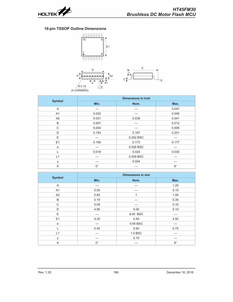
Rev. 1.20 18� De�e��e� 1�� 201� Rev. 1.20 187 De�e��e� 1�� 201�
HT45FM30Brushless DC Motor Flash MCU
16-pin TSSOP Outline Dimensions
� �
��
� �
� �
� �
�� � � � � �� � � � � � � � � �
�
� �
�
� �
�
SymbolDimensions in inch
Min. Nom. Max.A — — 0.047
A1 0.002 — 0.00� A2 0.031 0.039 0.041 B 0.007 — 0.012 C 0.004 — 0.00� D 0.193 0.197 0.201 E — 0.252 BSC —
E1 0.1�9 0.173 0.177 e — 0.02� BSC —L 0.018 0.024 0.030
L1 — 0.039 BSC —y — 0.004 —θ 0° — 8°
SymbolDimensions in mm
Min. Nom. Max.A — — 1.20
A1 0.05 — 0.15 A2 0.80 1 1.05 B 0.19 — 0.30 C 0.09 — 0.1� D 4.90 5.00 5.10E — �.40 BSC —
E1 4.30 4.40 4.50 e — 0.�5 BSC —L 0.45 0.�0 0.75
L1 — 1.0 BSC —y — 0.10 —θ 0° — 8°
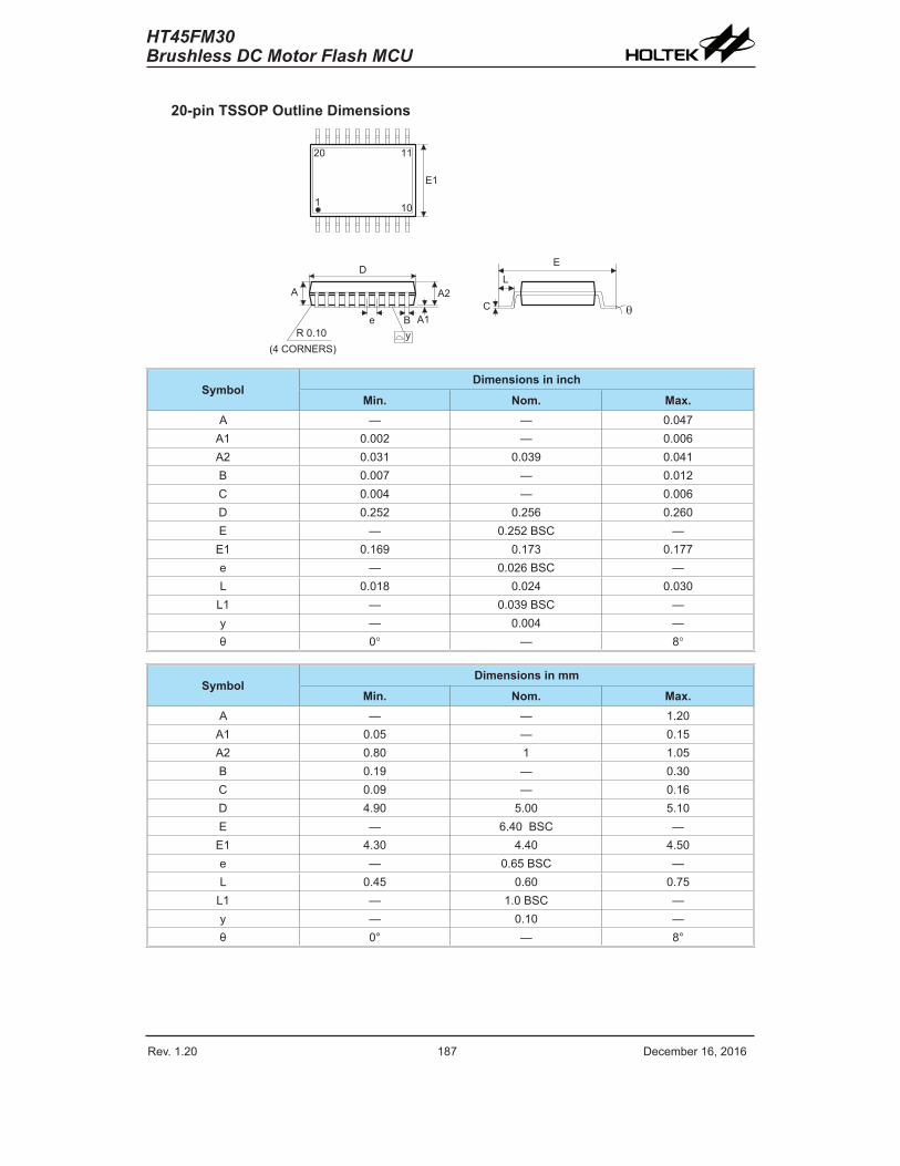
Rev. 1.20 18� De�e��e� 1�� 201� Rev. 1.20 187 De�e��e� 1�� 201�
HT45FM30Brushless DC Motor Flash MCU
20-pin TSSOP Outline Dimensions
� �
��
� �
� �
� �
�� � � � � �� � � � � � � � � �
�
� �
�
� � �
� �� �
SymbolDimensions in inch
Min. Nom. Max.A — — 0.047
A1 0.002 — 0.00� A2 0.031 0.039 0.041 B 0.007 — 0.012 C 0.004 — 0.00� D 0.252 0.25� 0.2�0 E — 0.252 BSC —
E1 0.1�9 0.173 0.177 e — 0.02� BSC —L 0.018 0.024 0.030
L1 — 0.039 BSC —y — 0.004 —θ 0° — 8°
SymbolDimensions in mm
Min. Nom. Max.A — — 1.20
A1 0.05 — 0.15 A2 0.80 1 1.05 B 0.19 — 0.30 C 0.09 — 0.1� D 4.90 5.00 5.10E — �.40 BSC —
E1 4.30 4.40 4.50 e — 0.�5 BSC —L 0.45 0.�0 0.75
L1 — 1.0 BSC —y — 0.10 —θ 0° — 8°
Rev. 1.20 188 De�e��e� 1�� 201� Rev. 1.20 PB De�e��e� 1�� 201�
HT45FM30Brushless DC Motor Flash MCU
Copy�ight© 201� �y HOLTEK SEMICONDUCTOR INC.
The info��ation appea�ing in this Data Sheet is �elieved to �e a��u�ate at the ti�e of pu�li�ation. Howeve�� Holtek assu�es no �esponsi�ility a�ising f�o� the use of the specifications described. The applications mentioned herein are used solely fo� the pu�pose of illust�ation and Holtek �akes no wa��anty o� �ep�esentation that su�h appli�ations will �e suita�le without fu�the� �odifi�ation� no� �e�o��ends the use of its p�odu�ts fo� appli�ation that �ay p�esent a �isk to hu�an life due to �alfun�tion o� othe�wise. Holtek's p�odu�ts a�e not autho�ized fo� use as ��iti�al �o�ponents in life suppo�t devi�es o� syste�s. Holtek �ese�ves the �ight to alte� its products without prior notification. For the most up-to-date information, please visit ou� we� site at http://www.holtek.�o�.tw.