Embed Size (px)
Citation preview

Gondwana University, Gadchiroli
Proposed Syllabus
B.Sc. I
Subject: Electronics
Semester I & II
Board of Studies - Electronics
Gondwana University Gadchiroli
Scheme of Bachelor of Science for Semester Examination

Gondwana University, Gadchiroli
Subject: Electronics
Class
Sem
este
r
Pap
er
Teaching Scheme Per Week
Examination Scheme
Th
eory
Total
Pra
ctic
al
Theory Marks
Practical Marks
Total Marks
Paper Internal
Assessment
B. Sc. I
I
I 3 6 + 1T*
6
50
20
30
150 II 3 50
II
I 3 6 + 1T*
6
50 20
30
150
II 3 50
B. Sc. II
III
I 3 6 + 2T*
6
50 20
30
150
II 3 50
IV
I 3 6 + 2T*
6
50 20
30
150
II 3 50
B. Sc. III
V
I 3 6 + 2T*
6
50 20
30
150
II 3 50
VI
I 3 6 + 2T*
6
50 20
30
150
II 3 50
* Periods for Tutorials per batch.


Details of the Syllabus
First Year B.Sc.
Subject: Electronics
Scheme for Semester I
W.E.F. 2012-13
Paper
No. of Periods per week (48 minutes each)
Marks
Lecture
Practical
Tutorial
Theory Internal Assessment
Practical
Total
Paper – I Basic Electronics and Semiconductor Devices
3
6
1
50
20
30
150
Paper – II Transducers and Network Theorems
3
50
Paper I (Semester-I)
Basic Electronics and Semiconductor Devices
Unit - I
Introduction of Passive Components:-
Resistor: types, Construction and properties of carbon composition, wire-wound, film resistor.
Resistors in series and parallel.
Variable resistor: - Potentiometer, Rheostat and preset.
Capacitor: Construction and properties of paper, mica, ceramic and electrolytic.
Capacitors in series and parallel
Inductor: Concept of self and mutual inductance. Construction and properties of air core, iron
core and ferrite core.
Transformer: Construction and working, Types step-up and step down, power, isolation, auto
transformer
Unit - II
Concept of band diagram (Insulator, conductor and semiconductor)
Intrinsic and extrinsic semiconductor, PN junction, forward and reverse bias characteristics of
PN junction, transition capacitance, diffusion capacitance, Zener Diode, breakdown mechanism
(Avalanche effect, Zener effect). Diode as a half-wave, full-wave and bridge rectifier.

Unit- III
Construction and characteristics of BJT : NPN and PNP transistor, CB, CE & CC configuration,
leakage currents, Input and output characteristics of CE mode, relation between and β , Load
line (DC only) and operating point, amplification action of CE amplifier (Simple numerical
expected)
Unit- IV
Construction, working and characteristics of J-FET, comparison of BJT and FET, parameters of
JFET, JFET as an amplifier (common source). Construction and working of MOSFET (depletion
and enhancement), advantages and disadvantages of MOSFET
Construction, working and characteristics of SCR, SCR as a switch.
Construction, working, characteristics and advantages of TRIAC, DIAC and UJT.
Paper II (Semester-I)
Transducers and Network Theorems
Unit- I
Concept of transducer needs of transducers, definition of active and passive transducer, and
classification of transducer. Thermister, thermocouple, LVDT and piezoelectric transducer,
strain gauge, capacitive transducer, microphone and loudspeaker.
Unit- II
Construction and characteristics of optoelectronic devices: - Photovoltaic cell, photoconductive
cell, Solar cell, LDR, LED, LCD (dynamic scattering and field effect type), LASER diode.
Unit- III
Ideal voltage and current sources (AC and DC). Concept of node, mesh, loops in network,
voltage divider and current division method/Law Kirchhoff’s voltage law, Kirchhoff’s current.
Transformation of energy sources. Statement and proof of Superposition theorem (simple
numerical with DC sources only)
Unit- IV
Statement, explanation and proof of Thevenin’s theorem, Norton’s theorem , Millman’s theorem,
dual of Millman’s theorem and maximum power transfer theorem, (simple numerical with DC
sources only).

Internal Assessment (20 marks)
Marks
Attendance 05
Home assignment
Completion 05
Record 02
Seminar 05
Group discussion 03
PRACTICALS (conducted by internal examiner)
It is divided into two sections i.e. Section-A and Section-B. At least five experiments from each
section must be performed and the practical record book duly signed should be submitted at the
time of examination. Each student is expected to perform one experiment from each section, in
the University Examination. The duration of practical examination is six hours.
Marks Distribution:
Record Experiment Viva Total
Section – A
3
9
3
15
Section – B 3 9 3 15
Total 30
Section A
1. Identification and testing of various electronic components.
2. Study of transformer.
3. Study of forward biased characteristics P-N junction (Ge / Si / LED) diode.
4. Study of reverse biased characteristics of Zener diode.
5. Study of half wave (HWR) rectifier with varying load.
6. Study of full wave (FWR) rectifier with varying load.
7. Study of bridge (FWR) rectifier with varying load.
8. Study of BJT in CE mode.
9. Study of FET characteristics.
10. Study of SCR characteristics.
11. Study of DIAC characteristics.
12. Study of TRIAC characteristics.

Section B 1. Study of L.D.R. characteristics.
2. Study of Thermister (NTC/PTC) characteristics.
3. Study of LVDT characteristics.
4. Study of microphone and loudspeaker.
5. Study of photovoltaic cell.
6. Study of Kirchhoff’s voltage law.
7. Study of Superposition theorem.
8. Study of Thevenin’s theorem.
9. Study of Maximum power transfer theorem.
10. Study of Millman’s theorem.
Note: An Industrial visit / Study tour should be arranged for the student after semester-I.
Reference Books
1. Basic electronics – Grob
2. Basic electronics – B.L. Thereja
3. Principle of electronics - V. K. Mehta
4. Electronic Devices and Circuits- Allen Mottershed
5. Electronics, fundamental and Application – Ryder
6. Electronics, Discrete and integrated Circuits – Y.M.Bapat
7. Basic electronics Linear Circuits – R.N.Bhargawa
8. Principle Electronics - Malvino
9. Elements of Electronics – Bagade & Singh
10. Electronic and Electrical Measurement and instrumentation- A. K. Sawhney
11. Electronics Instrument and Measurement Technology –W.D.Cooper
12. Network Analysis G.K. Mittal

Gondwana University, Gadchiroli
First Year B.Sc. Subject:
Electronics Scheme for
Semester II
W.E.F. 2012-13
Paper
No. of Periods per week (48 minutes each)
Marks
Lecture
Practical
Tutorial
Theory Internal Assessment
Practical
Total
Paper – I Digital Electronics and Computer Fundamentals
3
6
1
50
20
30
150
Paper – II Measuring Devices
3
50
Details of the Syllabus Paper I (Semester-II)
Digital Electronics and Computer Fundamentals
Unit-I
Number system – decimal, binary, octal, hexadecimal, representation of integer fraction and
mixed number and their mutual conversion
Complement number – 1’s and 2’s complement, subtraction by 1’s and 2’s complement, 9’s and
10’s complement, subtraction by 9’s and 10’s complement.
Sign magnitude number: 1’s and 2’s Complement representation.
Unit-II
Codes – BCD-8421, Excess 3, parity code and grey code
Basic logic gate – NOT, OR, AND
Universal gates NOR and NAND,
EX-OR and EX-NOR gate and their truth tables. Application of EX-OR gate as controlled
inverter.
Boolean laws: basic laws, simplification, Statement and proof of Demorgan’s theorem and
duality theorem.

Unit-III
Logic families: Classification of logic families, characteristics (Fan-in, Fan-out, Noise immunity,
propagation delay, Power dissipation. Construction and working of TTL NAND and NOR gate,
construction and working of CMOS NAND and NOR gates, concept of tristate logic, Comparison
of TTL and CMOS logic families with respect to propagation delay, power consumption, noise
immunity, fan in and fan out.
Unit-IV
Block diagram of computer, function of each block, types of computer (digital, analog and
hybrid), classification of computer, computer generation.
Input devices - key board, mouse, scanner
Output devices – printer: - lines, character (Dot matrix), page (LASER).
I/O devices – Pen drive, hard disk, optical disk.
Application of computer
Unit- I
Semester-II
Paper II
Measuring Devices
Introduction to galvanometer (PMMC), conversion of PMMC to voltmeter, ammeter, ohmmeter
(Series and shunt). Concept of loading effect and sensitivity, concept of multimeter. (Simple
numerical expected)
Unit-II
Construction and working of EVM using FET.
Construction, working and advantages of digital multimeter.
Brides - general condition of balance of AC bridge, Owen bride Schering bridge. (simple
numerical expected)
Unit-III
Block diagram of CRO, CRT diagram, electrostatic focusing, deflection sensitivity, and
horizontal and vertical deflection system. Time base circuit using UJT, needs of delay line.
Concept of synchronization.
Unit-IV
Applications of CRO for voltage, frequency and phase measurement. Concept and block
diagram of dual trace CRO. CRO probes (passive only), comparison of dual trace and dual
beam CRO.

Internal Assessment (20 marks)
Marks
Attendance 05
Home assignment
Completion 05
Record 02
Seminar 05
Group discussion 03
PRACTICALS (conducted by internal and external examiner)
It is divided into two sections i.e. Section-A and Section-B. At least five experiments from each
section must be performed and the practical record book duly signed should be submitted at the
time of examination. Each student is expected to perform one experiment from each section, in
the University Examination. The duration of practical examination is six hours.
Marks Distribution:
Report Experiment Viva Total
Section – A
3
9
3
15
Section – B 3 9 3 15
Total 30
Section A
1 Study of basic logic gate.
2 Study of NAND gate as a universal gate
3 Study of NOR gate as a universal gate
4 Study of Ex – OR gate
5 Study of Ex – NOR gate
6 Verification of truth Table for given Boolean expression.
7 Study of Demorgan’s theorem
8 Study of Input devices: Keyboard and Mouse.
9 Study of Input devices: Scanner and Printer.
Section B
1. Study of Series type Ohmmeter
2. Study of Shunt type Ohmmeter
3. Study of DC multirange Ammeter.
4. Study of DC multirange Voltmeter.
5. Study of loading effect in Voltmeter (DC only).
6. Study of Schering Bridge.
7. Study of Owen’s bridge.
8. Study/Use of CRO for measurement of voltage and frequency.
9. Study/Use of CRO for determination of frequency and phase.
Reference Books
1. Digital and Analogue technique – Kale & Navaneet
2. Digital Principle and application – Malvino & Leach
3. Modern digital electronics – R.P. Jain
4. Electronics devices & circuits –Jocob Milliman & C.C. Hulkiyas
5. Introduction to Computer –Rajaraman
6. Introduction to Computer Science: –Satish Jain
7. Computer Fundamentals – P. K. Sinha
8. Electronics Instrument and Measurement Technology –W.D.Cooper
9. Electronic and Electrical Measurement and instrumentation- A.K. Sawhney
10. Basic electronics – B.L. Thereja
11. Modern Electronics Equipment: Trouble Shooting Repair and Maintenance: R.C. Khanpur.
B) Absorption scheme:
1. While switch over to the semester system, failure students should get three chances to clear yearly
pattern.
2. To get admission in the third semester students should clear first semester including theory as well
as practical
1. First year annual pattern students shall get admission to third semester directly.
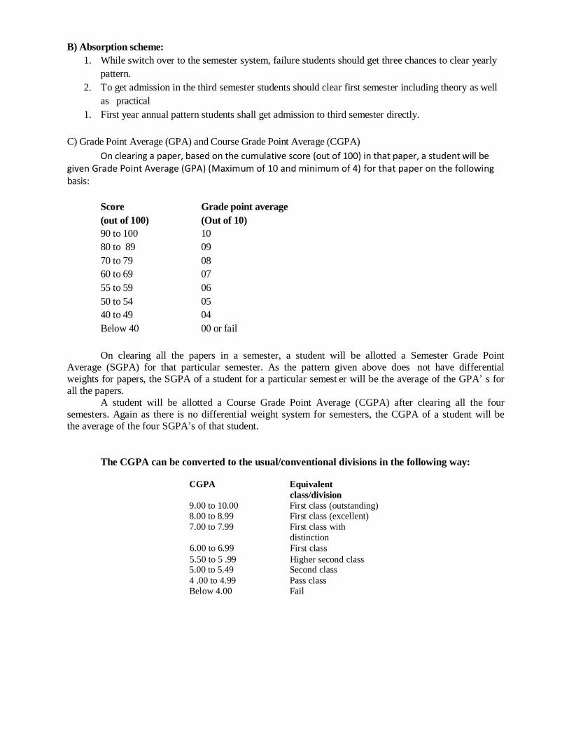
C) Grade Point Average (GPA) and Course Grade Point Average (CGPA)
On clearing a paper, based on the cumulative score (out of 100) in that paper, a student will be given Grade Point Average (GPA) (Maximum of 10 and minimum of 4) for that paper on the following basis:
Score Grade point average
(out of 100) (Out of 10)
90 to 100 10
80 to 89 09
70 to 79 08
60 to 69 07
55 to 59 06
50 to 54 05
40 to 49 04
Below 40 00 or fail
On clearing all the papers in a semester, a student will be allotted a Semester Grade Point
Average (SGPA) for that particular semester. As the pattern given above does not have differential
weights for papers, the SGPA of a student for a particular semest er will be the average of the GPA’ s for
all the papers.
A student will be allotted a Course Grade Point Average (CGPA) after clearing all the four
semesters. Again as there is no differential weight system for semesters, the CGPA of a student will be
the average of the four SGPA’s of that student.
The CGPA can be converted to the usual/conventional divisions in the following way:
CGPA Equivalent
class/division
9.00 to 10.00 First class (outstanding) 8.00 to 8.99 First class (excellent)
7.00 to 7.99 First class with
distinction
6.00 to 6.99
5.50 to 5 .99
First class
Higher second class
5.00 to 5.49 Second class
4 .00 to 4.99 Pass class Below 4.00 Fail


![TheChinaSyndrome: LocalLaborMarketEffectsof ... · ujt j i + h ln ˝ cnjt ˝ unjt n i [ln z cjt z ujt j] isChina’srelativeTFPinindustryj yeart [ ln ˝ cnjt ˝ unjt n] isChina’srel](https://img.pdfslide.net/doc/110x75/5e92fe1ef15bf82da619a3e4/thechinasyndrome-locallabormarketeiectsof-ujt-j-i-h-ln-cnjt-unjt.jpg)