Embed Size (px)
Citation preview
Manonmaniam Sundaranar University, Directorate of Distance & Continuing Education, Tirunelveli. 1
B.Sc. PHYSICS – I YEAR
DJK1B : BASIC ELECTRONICS
SYLLABUS
Unit I : Diodes
P-n junction diode – characteristics – Regulation with zener diodes – Bridge rectifier –
clipping and clamping circuits with diodes.
Unit II : Transistors and Amplifiers
Transistors – Transistor action – three modes of connection – biasing – load line and Q –point
– voltage divider bias – stabilization – CE amplifier.
Unit III : Oscillators
Principles of negative voltage feed back in amplifiers – gain – advantages – principle of
negative current feedback – Oscillation – Bark Hausen criterion for oscillation – colpitt’s
oscillator
Unit IV : Field Effect Transistor
Principle , features and characteristics of FET – JFET and MOSFET – their characteristics –
enhancement and depletion type
Unit V : Operational Amplifier
Characteristics – slew rate – inverting and non-inverting amplifier – adder – sub tractor –
integrator – differentiator
Books for study and reference:
1. Fundamentals of Electronics – B. Ghosh
2. Principles of Electronics - V.K. Mehtha
Manonmaniam Sundaranar University, Directorate of Distance & Continuing Education, Tirunelveli. 2
UNIT I : DIODES
P-N junction diode – characteristics – Regulation with zener diodes – Bridge rectifier –
clipping and clamping circuits with diodes.
1.1 Semiconductors
Semiconductor is a solid substance that has a conductivity between that of an
insulator and that of metal due to the addition of an impurity. Devices made of
semiconductors, are the essential components of most electronic circuits. Semiconductors
include antimony, arsenic, boron, carbon, germanium, selenium, silicon, sulfur, and
tellurium. Silicon is the best-known of these, forming the basis of most integrated circuits .
Common semiconductor compounds include gallium arsenide, indium antimonide, and the
oxides of most metals. Of these, gallium arsenide (Ga-As) is widely used in low-noise, high-
gain, weak-signal amplifying devices.
Types of Semiconductors: Semiconductors are mainly classified into two categories: They
are (a) Intrinsic Semiconductors and (b) Extrinsic Semiconductors
(a) Intrinsic Semiconductor
An electron is called a negative charge carrier and a hole ( absence of an electron) is
called a positive charge carrier. An intrinsic semiconductor material is chemically very pure
and possesses poor conductivity. It has equal numbers of negative charge carriers and
positive charge carriers. A silicon crystal is different from an insulator because at any
temperature above absolute zero, there is a finite probability that an electron in the lattice
will be knocked loose from its position, leaving behind an electron deficiency or a hole.
If a voltage is applied, then both the electron and the hole can contribute to a small
current flow. The conductivity of a semiconductor can be modelled in terms of the band
theory of solids. The band model of a semiconductor suggests that at ordinary temperatures
there is a finite probability that electrons can reach the conduction band and contribute to
electrical conduction.
Manonmaniam Sundaranar University, Directorate of Distance & Continuing Education, Tirunelveli. 3
(b) Extrinsic Semiconductor
An extrinsic semiconductor is an improved intrinsic semiconductor with a small
amount of impurities added by a process, known as doping. This alters the electrical
properties of the semiconductor and improves its conductivity. Introducing impurities into
the semiconductor materials can control their conductivity. Doping process produces two
groups of semiconductors: the majority negative charge conductor (n-type) and the positive
charge conductor (p-type). Semiconductors are available as either elements or compounds.
Silicon and Germanium are the most common elemental semiconductors.
1.2 Doping of Semiconductors
Pentavalent impurities (5-valence electrons) produce n-type semiconductors by contributing
extra electrons. Trivalent impurities (3-valence electrons) produce p-type semiconductors by
producing a hole or electron deficiency.
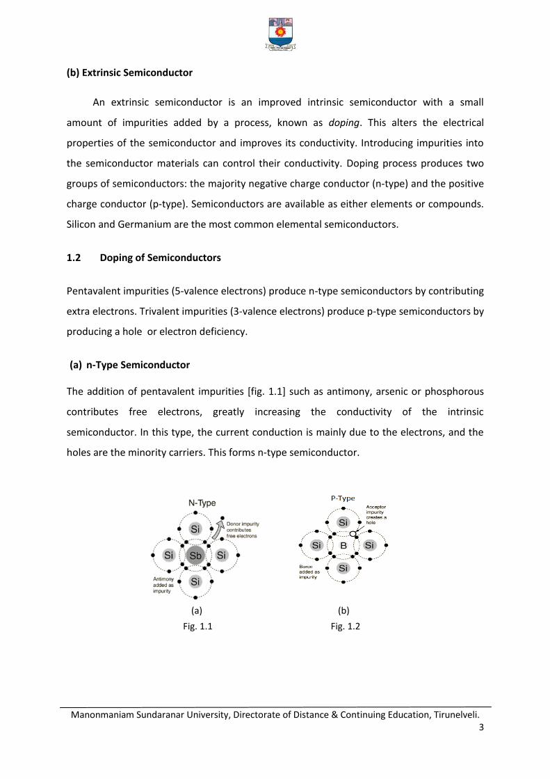
(a) n-Type Semiconductor
The addition of pentavalent impurities [fig. 1.1] such as antimony, arsenic or phosphorous
contributes free electrons, greatly increasing the conductivity of the intrinsic
semiconductor. In this type, the current conduction is mainly due to the electrons, and the
holes are the minority carriers. This forms n-type semiconductor.
Fig. 1.1
(b) (a)
Fig. 1.2
Manonmaniam Sundaranar University, Directorate of Distance & Continuing Education, Tirunelveli. 4
(b) p-Type Semiconductor
The addition of trivalent impurities [fig. 1.2] such as boron, aluminum or gallium to an
intrinsic semiconductor creates deficiencies of valence electrons, called holes. In this type,
the current conduction is mainly due to the holes, and the electrons are the minority
carriers. This forms p-type semiconductor.
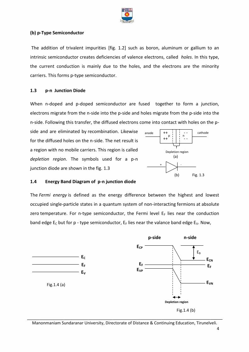
1.3 p-n Junction Diode
When n-doped and p-doped semiconductor are fused together to form a junction,
electrons migrate from the n-side into the p-side and holes migrate from the p-side into the
n-side. Following this transfer, the diffused electrons come into contact with holes on the p-
side and are eliminated by recombination. Likewise
for the diffused holes on the n-side. The net result is
a region with no mobile carriers. This region is called
depletion region. The symbols used for a p-n
junction diode are shown in the fig. 1.3
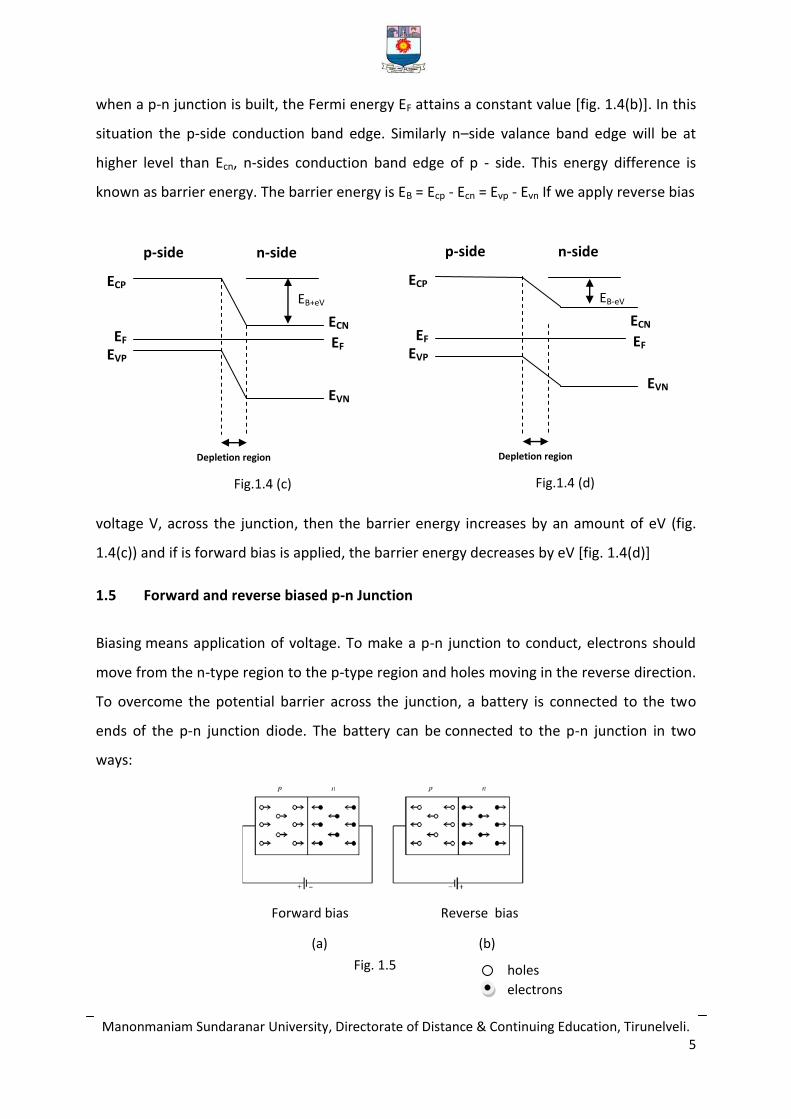
1.4 Energy Band Diagram of p-n junction diode
The Fermi energy is defined as the energy difference between the highest and lowest
occupied single-particle states in a quantum system of non-interacting fermions at absolute
zero temperature. For n-type semiconductor, the Fermi level EF lies near the conduction
band edge EC but for p - type semiconductor, EF lies near the valance band edge EV. Now,
ECP
EF
EVP
ECN
EF
EVN
p-side n-side
Depletion region
EF
EV
EC
Fig.1.4 (a)
Fig.1.4 (b)
EB
++
++
- -
- -
Depletion region
p n anode cathode
+ -
Fig. 1.3
(a)
(b)
Manonmaniam Sundaranar University, Directorate of Distance & Continuing Education, Tirunelveli. 5
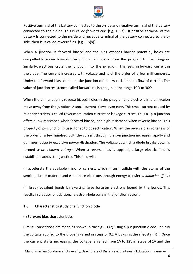
when a p-n junction is built, the Fermi energy EF attains a constant value [fig. 1.4(b)]. In this
situation the p-side conduction band edge. Similarly n–side valance band edge will be at
higher level than Ecn, n-sides conduction band edge of p - side. This energy difference is
known as barrier energy. The barrier energy is EB = Ecp - Ecn = Evp - Evn If we apply reverse bias
voltage V, across the junction, then the barrier energy increases by an amount of eV (fig.
1.4(c)) and if is forward bias is applied, the barrier energy decreases by eV [fig. 1.4(d)]
1.5 Forward and reverse biased p-n Junction
Biasing means application of voltage. To make a p-n junction to conduct, electrons should
move from the n-type region to the p-type region and holes moving in the reverse direction.
To overcome the potential barrier across the junction, a battery is connected to the two
ends of the p-n junction diode. The battery can be connected to the p-n junction in two
ways:
ECP
EF
EVP
ECN
EF
EVN
p-side n-side
Depletion region
Fig.1.4 (c)
EB+eV
ECP
EF
EVP
ECN
EF
EVN
p-side n-side
Depletion region
Fig.1.4 (d)
EB-eV
Fig. 1.5
(a) (b)
holes
electrons
Forward bias Reverse bias
Manonmaniam Sundaranar University, Directorate of Distance & Continuing Education, Tirunelveli. 6
Positive terminal of the battery connected to the p-side and negative terminal of the battery
connected to the n-side. This is called forward bias [fig. 1.5(a)]. If positive terminal of the
battery is connected to the n-side and negative terminal of the battery connected to the p-
side, then it is called reverse bias [fig. 1.5(b)].
When a junction is forward biased and the bias exceeds barrier potential, holes are
compelled to move towards the junction and cross from the p-region to the n-region.
Similarly, electrons cross the junction into the p-region. This sets in forward current in
the diode. The current increases with voltage and is of the order of a few milli-amperes.
Under the forward bias condition, the junction offers low resistance to flow of current. The
value of junction resistance, called forward resistance, is in the range 10Ω to 30Ω.
When the p-n junction is reverse biased, holes in the p-region and electrons in the n-region
move away from the junction. A small current flows even now. This small current caused by
minority carriers is called reverse saturation current or leakage current. Thus a p-n junction
offers a low resistance when forward biased, and high resistance when reverse biased. This
property of p-n junction is used for ac to dc rectification. When the reverse bias voltage is of
the order of a few hundred volt, the current through the p-n junction increases rapidly and
damages it due to excessive power dissipation. The voltage at which a diode breaks down is
termed as breakdown voltage. When a reverse bias is applied, a large electric field is
established across the junction. This field will:
(i) accelerate the available minority carriers, which in turn, collide with the atoms of the
semiconductor material and eject more electrons through energy transfer (avalanche effect)
(ii) break covalent bonds by exerting large force on electrons bound by the bonds. This
results in creation of additional electron-hole pairs in the junction region .
1.6 Characteristics study of a junction diode
(i) Forward bias characteristics
Circuit Connections are made as shown in the fig. 1.6(a) using a p-n junction diode. Initially
the voltage applied to the diode is varied in steps of 0.1 V by using the rheostat (Rh). Once
the current starts increasing, the voltage is varied from 1V to 12V in steps of 1V and the
Fig. 1.5
Manonmaniam Sundaranar University, Directorate of Distance & Continuing Education, Tirunelveli. 7
corresponding forward biased voltage readings (Vf) in the voltmeter (V) and the
corresponding forward biased current (If) in the milli ammeter (mA) are noted and the
readings are tabulated as shown in the table. A suitable graph is drawn by taking Vf on x-axis
and If on y-axis. This gives the forward bias characteristic curve.
(ii) Reverse bias characteristics
To study the reverse bias characteristics of the diode, a circuit connection is made as shown
in the fig. 1.6(a), but with the polarities of the diode are changed and the milliammeter is
replaced with a micro ammeter. The procedure is repeated as in forward bias mode and the
readings are tabulated. A suitable graph is drawn giving the reverse bias characteristic curve
for the given p-n diode.
TABLE 1
The characteristic curve for a p-n junction diode is shown in the fig.1.6 (b). In the forward
bias mode, the current increases very slowly in the beginning and then increases rapidly.
S.No. Forward / Reverse bias in
volts
Forward bias/Reverse bias
current in mA/ µA
Forward bias
Reverse bias
I (mA)
I (µA)
Knee voltage
Fig. 1.6(b)
Fig. 1.6(a)
Breakdown voltage
Manonmaniam Sundaranar University, Directorate of Distance & Continuing Education, Tirunelveli. 8
The point at which the current starts to increase rapidly is known as knee voltage. In the
reverse mode, the current increases with voltage and reaches a point where it remains
almost constant with further increase in voltage. This voltage is called break down voltage of
the given diode.
1.7 Zener Diode
A Zener Diode is a special kind of diode which permits current to flow in the forward
direction as normal, but will also allow it to flow in the reverse direction when the voltage is
above a certain value, the breakdown voltage known as the Zener voltage. The symbol used
is shown in the fig. 1.7(a)
Fig. 1.7 (a)
Fig. 1.7 (b)
The zener voltage of a standard diode is high, but if a reverse current above that value is
allowed to pass through it, the diode is permanently damaged. Zener diodes are designed so
that, when a reverse current above the zener voltage passes through a zener diode, there is a
controlled breakdown which does not damage the diode. The voltage drop across the zener
diode is equal to the zener voltage of that diode. The fig. 1.7 (b) shows a current vs. voltage
graph. With a zener diode connected in the forward direction, it behaves exactly the same as a
standard diode. In the reverse direction however there is a very small leakage
current between 0V and the zener break down voltage. Then, when the voltage reaches
the breakdown voltage (Vz), suddenly current flows freely through it.
Breakdown voltage
voltage
current
Forward bias
Avalanche current
leakage current
Vz
0
Reverse bias
Manonmaniam Sundaranar University, Directorate of Distance & Continuing Education, Tirunelveli. 9
Uses of Zener Diodes
1) They are used as reference voltages for circuits.
2) Zener diodes are used to regulate the voltage in electric circuits.
3) They are used as over voltage protector.
1.8 Zener Diode as Voltage Regulator
A voltage regulator circuit can be designed using a zener diode to maintain a constant DC
output voltage across the load in spite of variations in the input voltage or changes in the
load current. The zener diode is always operated in its reverse biased condition.
In the fig. (1.8), by using Kirchoff’s current law, we can write
Lzs III
If LI decreases due to change in load resistance, zI increases since sI is constant. Even
then Vz remains constant. When LI increases, zI decreases to keep sI constant. Thus Vz
is always constant. That is the voltage across the load is always constant.
Also, when Vs exceeds the rated voltage of the device, the breakdown voltage is reached at
which avalanche breakdown occurs in the semiconductor depletion layer of the zener diode
and a current starts to flow through the diode, thus maintaining a constant current flow
Fig. 1.8
Manonmaniam Sundaranar University, Directorate of Distance & Continuing Education, Tirunelveli. 10
through the load. The current now flowing through the zener diode increases dramatically
to the maximum circuit value, which is usually limited by a series resistor and once achieved
this reverse saturation current remains constant over a wide range of applied voltages. The
voltage point at which the voltage across the zener diode becomes stable is called the zener
voltage. For zener diodes this voltage can range from less than one volt to hundreds of
volts.
1.9 Bridge Rectifier
Construction
A Bridge rectifier is an alternating current (AC) to direct current (DC) converter. The
bridge rectifier circuit diagram is shown in the fig. 1.9. It consists of a step down
transformer which converts the AC mains 230V to 12V AC supply. Next stage uses four
diodes in the form of a bridge as shown. Since the output after the diode bridge rectifiers is
of pulsating, a filter circuit is used. The filter consists of one or more capacitors across the
load.
Fig.1.9
Working
During the positive half cycle of secondary voltage, diodes D2 and D3 are forward
biased and diodes D1 and D4 are reverse biased. Now the current flows through D2, Load
(RL) and D3. During the negative half cycle of the secondary voltage, diodes D1 and D4 are
forward biased and rectifier diodes D2 and D3 are reverse biased. Now the current flows
12 V
Fig. 1.10
Manonmaniam Sundaranar University, Directorate of Distance & Continuing Education, Tirunelveli. 11
through D4, Load and D1. In both the cycles, load current flows in the same direction.
Hence we get a pulsating DC voltage as shown in fig 1.10. So a filter circuit is added to
reduce the pulsation in the output wave form.
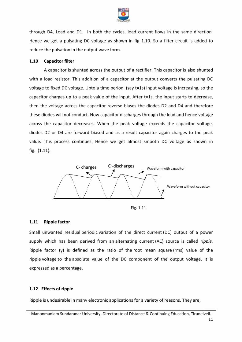
1.10 Capacitor filter
A capacitor is shunted across the output of a rectifier. This capacitor is also shunted
with a load resistor. This addition of a capacitor at the output converts the pulsating DC
voltage to fixed DC voltage. Upto a time period (say t=1s) input voltage is increasing, so the
capacitor charges up to a peak value of the input. After t=1s, the input starts to decrease,
then the voltage across the capacitor reverse biases the diodes D2 and D4 and therefore
these diodes will not conduct. Now capacitor discharges through the load and hence voltage
across the capacitor decreases. When the peak voltage exceeds the capacitor voltage,
diodes D2 or D4 are forward biased and as a result capacitor again charges to the peak
value. This process continues. Hence we get almost smooth DC voltage as shown in
fig. (1.11).
1.11 Ripple factor
Small unwanted residual periodic variation of the direct current (DC) output of a power
supply which has been derived from an alternating current (AC) source is called ripple.
Ripple factor (γ) is defined as the ratio of the root mean square (rms) value of the
ripple voltage to the absolute value of the DC component of the output voltage. It is
expressed as a percentage.
1.12 Effects of ripple
Ripple is undesirable in many electronic applications for a variety of reasons. They are,
C- charges C -discharges Waveform with capacitor
Waveform without capacitor
Fig. 1.11
Manonmaniam Sundaranar University, Directorate of Distance & Continuing Education, Tirunelveli. 12
1) The ripple frequency and its harmonics are within the audio band and will therefore
be audible on equipment such as radio receivers, equipment for playing recordings
and professional studio equipment.
2) The ripple frequency is within television video bandwidth. Analogue TV receivers will
exhibit a pattern of moving wavy lines if too much ripple is present.
3) The presence of ripple can reduce the resolution of electronic test and measurement
instruments. In an oscilloscope, it will manifest itself as a visible pattern on screen.
4) Within digital circuits, it reduces the threshold, at which logic circuits give incorrect
outputs and data is corrupted.
5) High-amplitude ripple currents shorten the life of electrolytic capacitors.
1.13 Peak Inverse Voltage (PIV)
Peak Inverse Voltage or Peak Reverse Voltage (PRV) refers to the maximum voltage a diode
or other device can withstand in the reverse-biased direction before it breaksdown. In a
rectifier circuit, during negative half cycle, the diode is reverse biased and the whole input
voltage appears across the diode. When the input reaches its peak value Vm, in the negative
half cycle, the voltage across the diode is maximum. This is the PIV of the given diode. In
rectifier design two important parameters must be considered.
1. The current handling capacity required of the diode
2. Peak Inverse Voltage that the diode must withstand without breakdown. It is
desirable to select a diode having reverse breakdown voltage at least 50% more than that
the expected PIV.
PROBLEM
The turn ratio of the transformer used in a bridge rectifier is 12:1. The primary is
connected to 220V, 50 Hz power. Assuming the diodes to be ideal, find the dc voltage
across the load. What is the PIV of each diode?
Given: VVrms 220
Maximum primary voltage= VVV rmsP 3112
Manonmaniam Sundaranar University, Directorate of Distance & Continuing Education, Tirunelveli. 13
If the maximum secondary voltage is Vs , then
1
12
S
P
V
V (since the turn ratio is 12:1)
9.2512
311
12
1 PS VV volts
PIV= 9.25SV V
d.c.voltage across the load= VV
V sdc 48.16
14.3
9.2522
PROBLEM
A power supply delivers 90 watts to a load of 1 kilo ohms. Find the a.c. voltage
present across the load, if the ripple factor is 0.1%
Power delivered to the load
VV
V
PRVorR
VP
dc 300
300100090
2
since P=90 and R=1000
Ripple factor 3.0300100
1.0 dcac
dc
ac VrVorV
V V
1.14 Diode Clipping Circuits
The Diode Clipper, also known as a Diode Limiter, is a wave shaping circuit. It prevents the
output of a circuit from exceeding a predetermined voltage level without distorting the
remaining part of the applied waveform. It consists of resistors , junction diodes or
transistors. Clipping is achieved either at one level or two levels.
(a) Positive Diode Clipping Circuits
In this diode clipping circuit fig. 1.12, the diode is forward biased during the positive half
cycle of the sinusoidal input waveform. For the silicon diode to become forward biased, it
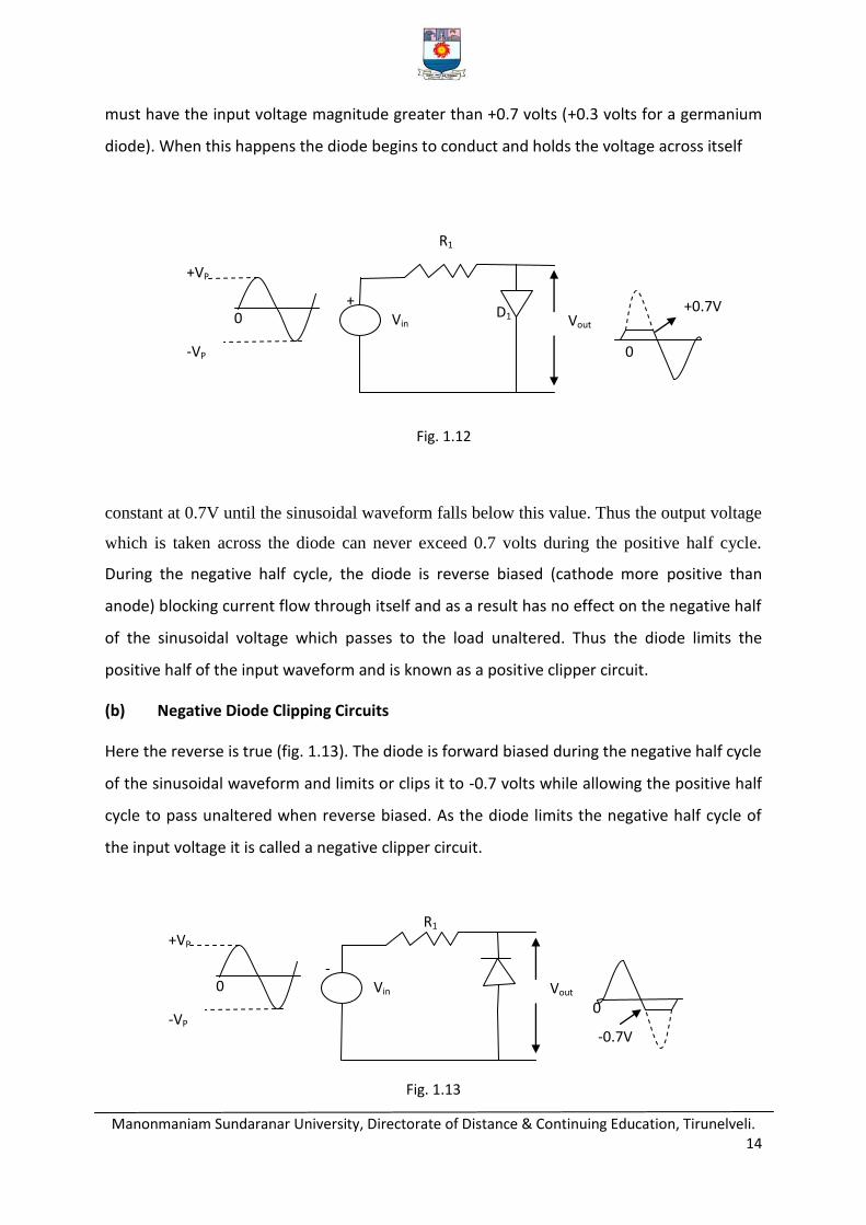
Manonmaniam Sundaranar University, Directorate of Distance & Continuing Education, Tirunelveli. 14
must have the input voltage magnitude greater than +0.7 volts (+0.3 volts for a germanium
diode). When this happens the diode begins to conduct and holds the voltage across itself
constant at 0.7V until the sinusoidal waveform falls below this value. Thus the output voltage
which is taken across the diode can never exceed 0.7 volts during the positive half cycle.
During the negative half cycle, the diode is reverse biased (cathode more positive than
anode) blocking current flow through itself and as a result has no effect on the negative half
of the sinusoidal voltage which passes to the load unaltered. Thus the diode limits the
positive half of the input waveform and is known as a positive clipper circuit.
(b) Negative Diode Clipping Circuits
Here the reverse is true (fig. 1.13). The diode is forward biased during the negative half cycle
of the sinusoidal waveform and limits or clips it to -0.7 volts while allowing the positive half
cycle to pass unaltered when reverse biased. As the diode limits the negative half cycle of
the input voltage it is called a negative clipper circuit.
Fig. 1.12
Fig. 1.13
Vin Vout
R1
-
-VP
+VP
0
0
-0.7V
Vin Vout D1
R1
+
-VP
+VP
+0.7V 0
0
Manonmaniam Sundaranar University, Directorate of Distance & Continuing Education, Tirunelveli. 15
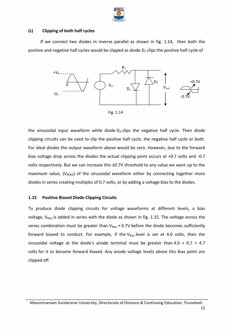
(c) Clipping of both half cycles
If we connect two diodes in inverse parallel as shown in fig. 1.14, then both the
positive and negative half cycles would be clipped as diode D1 clips the positive half cycle of
the sinusoidal input waveform while diode D2 clips the negative half cycle. Then diode
clipping circuits can be used to clip the positive half cycle, the negative half cycle or both.
For ideal diodes the output waveform above would be zero. However, due to the forward
bias voltage drop across the diodes the actual clipping point occurs at +0.7 volts and -0.7
volts respectively. But we can increase this ±0.7V threshold to any value we want up to the
maximum value, (VPEAK) of the sinusoidal waveform either by connecting together more
diodes in series creating multiples of 0.7 volts, or by adding a voltage bias to the diodes.
1.15 Positive Biased Diode Clipping Circuits
To produce diode clipping circuits for voltage waveforms at different levels, a bias
voltage, VBias is added in series with the diode as shown in fig. 1.15. The voltage across the
series combination must be greater than VBias + 0.7V before the diode becomes sufficiently
forward biased to conduct. For example, if the VBias level is set at 4.0 volts, then the
sinusoidal voltage at the diode’s anode terminal must be greater than 4.0 + 0.7 = 4.7
volts for it to become forward biased. Any anode voltage levels above this bias point are
clipped off.
Vin
R1
-VP
+VP
0 Vout D1
D2 +0.7V
-0.7V
Fig. 1.14
Manonmaniam Sundaranar University, Directorate of Distance & Continuing Education, Tirunelveli. 16
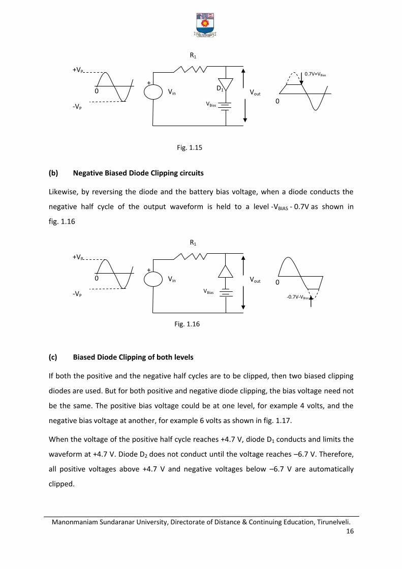
(b) Negative Biased Diode Clipping circuits
Likewise, by reversing the diode and the battery bias voltage, when a diode conducts the
negative half cycle of the output waveform is held to a level -VBIAS - 0.7V as shown in
fig. 1.16
(c) Biased Diode Clipping of both levels
If both the positive and the negative half cycles are to be clipped, then two biased clipping
diodes are used. But for both positive and negative diode clipping, the bias voltage need not
be the same. The positive bias voltage could be at one level, for example 4 volts, and the
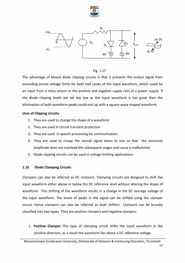
negative bias voltage at another, for example 6 volts as shown in fig. 1.17.
When the voltage of the positive half cycle reaches +4.7 V, diode D1 conducts and limits the
waveform at +4.7 V. Diode D2 does not conduct until the voltage reaches –6.7 V. Therefore,
all positive voltages above +4.7 V and negative voltages below –6.7 V are automatically
clipped.
R1
-VP
+VP
Vout 0 Vin
+
0
VBias -0.7V-VBias
Fig. 1.16
Vin Vout D1
R1
+
-VP
+VP
0
0.7V+VBias
0 VBias
Fig. 1.15
Manonmaniam Sundaranar University, Directorate of Distance & Continuing Education, Tirunelveli. 17
Fig. 1.17
The advantage of biased diode clipping circuits is that it prevents the output signal from
exceeding preset voltage limits for both half cycles of the input waveform, which could be
an input from a noisy sensor or the positive and negative supply rails of a power supply. If
the diode clipping levels are set too low or the input waveform is too great then the
elimination of both waveform peaks could end up with a square-wave shaped waveform.
Uses of Clipping circuits
1. They are used to change the shape of a waveform
2. They are used in Circuit transient protection
3. They are used in speech processing for communication
4. They are used to chopp the overall signal down to size so that the excessive
amplitude does not overload the subsequent stages and cause a malfunction
5. Diode clipping circuits can be used in voltage limiting applications.
1.16 Diode Clamping Circuits
Clampers can also be referred as DC restorers. Clamping circuits are designed to shift the
input waveform either above or below the DC reference level without altering the shape of
waveform. This shifting of the waveform results in a change in the DC average voltage of
the input waveform. The levels of peaks in the signal can be shifted using the clamper
circuit, hence clampers can also be referred as level shifters. Clampers can be broadly
classified into two types. They are positive clampers and negative clampers.
1. Positive Clamper: This type of clamping circuit shifts the input waveform in the
positive direction, as a result the waveform lies above a DC reference voltage.
-VP
+VP
+4.7V Vin
R1
0 Vout D1
D2
-6.7V 4V
6V
Manonmaniam Sundaranar University, Directorate of Distance & Continuing Education, Tirunelveli. 18
2. Negative Clamper: This type of clamping circuit shifts the input waveform in the
negative direction, as a result the waveform lies below a DC reference voltage.
The direction of the diode in the clamping circuit determines the type of clamper circuit. The
operation of a clamping circuit is mainly based on the switching time constants of the
capacitor. However, capacitor in the circuit charges through the diode and discharges
through the load.
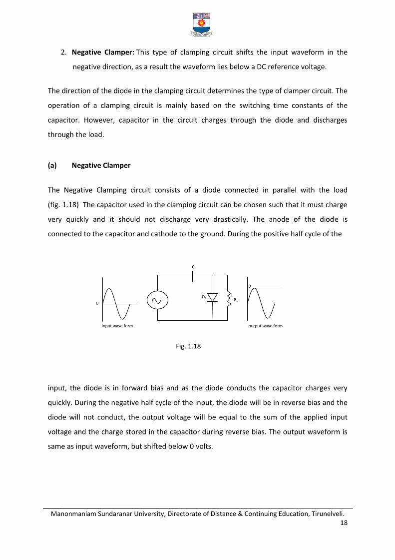
(a) Negative Clamper
The Negative Clamping circuit consists of a diode connected in parallel with the load
(fig. 1.18) The capacitor used in the clamping circuit can be chosen such that it must charge
very quickly and it should not discharge very drastically. The anode of the diode is
connected to the capacitor and cathode to the ground. During the positive half cycle of the
input, the diode is in forward bias and as the diode conducts the capacitor charges very
quickly. During the negative half cycle of the input, the diode will be in reverse bias and the
diode will not conduct, the output voltage will be equal to the sum of the applied input
voltage and the charge stored in the capacitor during reverse bias. The output waveform is
same as input waveform, but shifted below 0 volts.
output wave form
RL
C
D1
Input wave form
0
0
Fig. 1.18
Manonmaniam Sundaranar University, Directorate of Distance & Continuing Education, Tirunelveli. 19
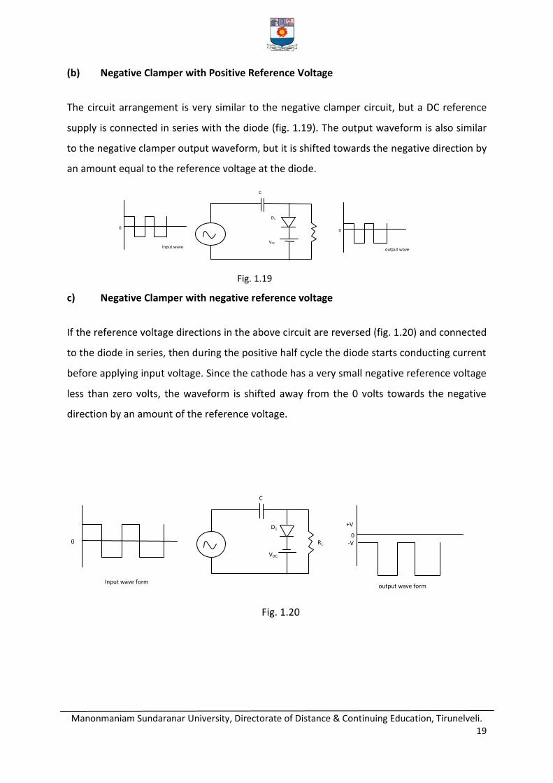
(b) Negative Clamper with Positive Reference Voltage
The circuit arrangement is very similar to the negative clamper circuit, but a DC reference
supply is connected in series with the diode (fig. 1.19). The output waveform is also similar
to the negative clamper output waveform, but it is shifted towards the negative direction by
an amount equal to the reference voltage at the diode.
c) Negative Clamper with negative reference voltage
If the reference voltage directions in the above circuit are reversed (fig. 1.20) and connected
to the diode in series, then during the positive half cycle the diode starts conducting current
before applying input voltage. Since the cathode has a very small negative reference voltage
less than zero volts, the waveform is shifted away from the 0 volts towards the negative
direction by an amount of the reference voltage.
output wave form
RL
Input wave form
+V
C
D1
VDC
0 0 -V
Fig. 1.20
Input wave
form
0
output wave
form
0
C
D1
VDC
Fig. 1.19
Manonmaniam Sundaranar University, Directorate of Distance & Continuing Education, Tirunelveli. 20
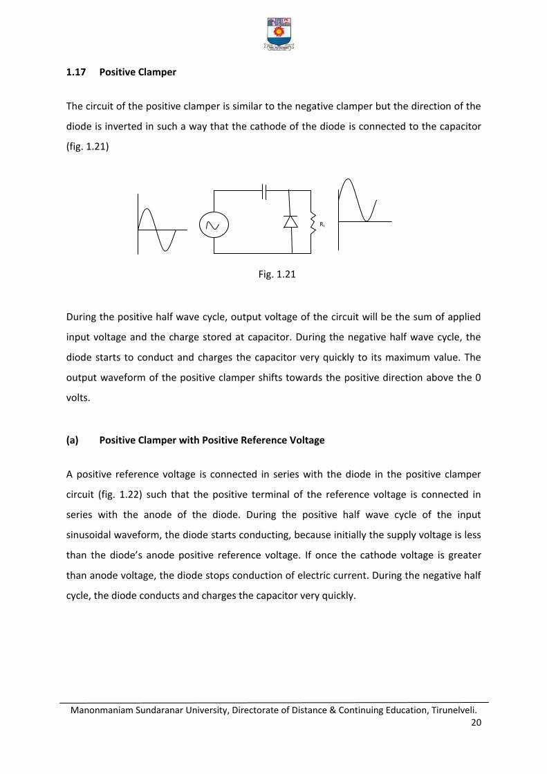
1.17 Positive Clamper
The circuit of the positive clamper is similar to the negative clamper but the direction of the
diode is inverted in such a way that the cathode of the diode is connected to the capacitor
(fig. 1.21)
Fig. 1.21
During the positive half wave cycle, output voltage of the circuit will be the sum of applied
input voltage and the charge stored at capacitor. During the negative half wave cycle, the
diode starts to conduct and charges the capacitor very quickly to its maximum value. The
output waveform of the positive clamper shifts towards the positive direction above the 0
volts.
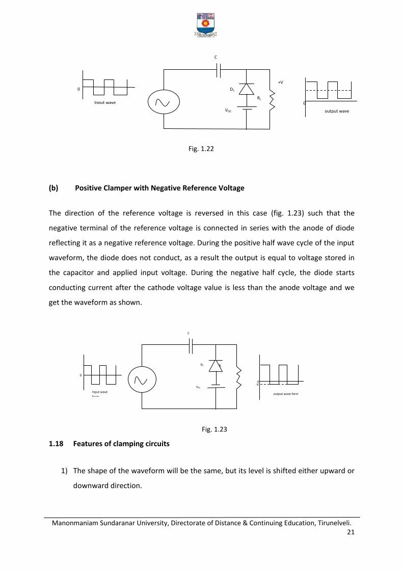
(a) Positive Clamper with Positive Reference Voltage
A positive reference voltage is connected in series with the diode in the positive clamper
circuit (fig. 1.22) such that the positive terminal of the reference voltage is connected in
series with the anode of the diode. During the positive half wave cycle of the input
sinusoidal waveform, the diode starts conducting, because initially the supply voltage is less
than the diode’s anode positive reference voltage. If once the cathode voltage is greater
than anode voltage, the diode stops conduction of electric current. During the negative half
cycle, the diode conducts and charges the capacitor very quickly.
RL
Manonmaniam Sundaranar University, Directorate of Distance & Continuing Education, Tirunelveli. 21
Fig. 1.22
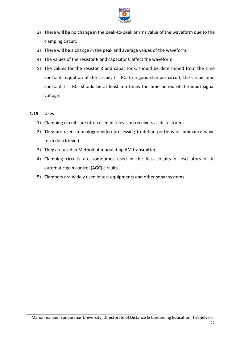
(b) Positive Clamper with Negative Reference Voltage
The direction of the reference voltage is reversed in this case (fig. 1.23) such that the
negative terminal of the reference voltage is connected in series with the anode of diode
reflecting it as a negative reference voltage. During the positive half wave cycle of the input
waveform, the diode does not conduct, as a result the output is equal to voltage stored in
the capacitor and applied input voltage. During the negative half cycle, the diode starts
conducting current after the cathode voltage value is less than the anode voltage and we
get the waveform as shown.
Fig. 1.23
1.18 Features of clamping circuits
1) The shape of the waveform will be the same, but its level is shifted either upward or
downward direction.
C
output wave form
RL
Input wave
form
0
VDC
D1
-V
0
RL
+V
Input wave
form
0
C
VDC
D1
output wave
form
0
Manonmaniam Sundaranar University, Directorate of Distance & Continuing Education, Tirunelveli. 22
2) There will be no change in the peak-to-peak or rms value of the waveform due to the
clamping circuit.
3) There will be a change in the peak and average values of the waveform.
4) The values of the resistor R and capacitor C affect the waveform.
5) The values for the resistor R and capacitor C should be determined from the time
constant equation of the circuit, t = RC. In a good clamper circuit, the circuit time
constant T = RC should be at least ten times the time period of the input signal
voltage.
1.19 Uses
1) Clamping circuits are often used in television receivers as dc restorers.
2) They are used in analogue video processing to define portions of luminance wave
form (black level)
3) They are used in Method of modulating AM transmitters
4) Clamping circuits are sometimes used in the bias circuits of oscillators or in
automatic gain control (AGC) circuits.
5) Clampers are widely used in test equipments and other sonar systems.
Manonmaniam Sundaranar University, Directorate of Distance & Continuing Education, Tirunelveli. 23
UNIT II : TRANSISTORS AND AMPLIFIERS
Transistors – Transistor action – three modes of connection – biasing – load line and Q –
point – voltage divider bias – stabilization – CE amplifier.
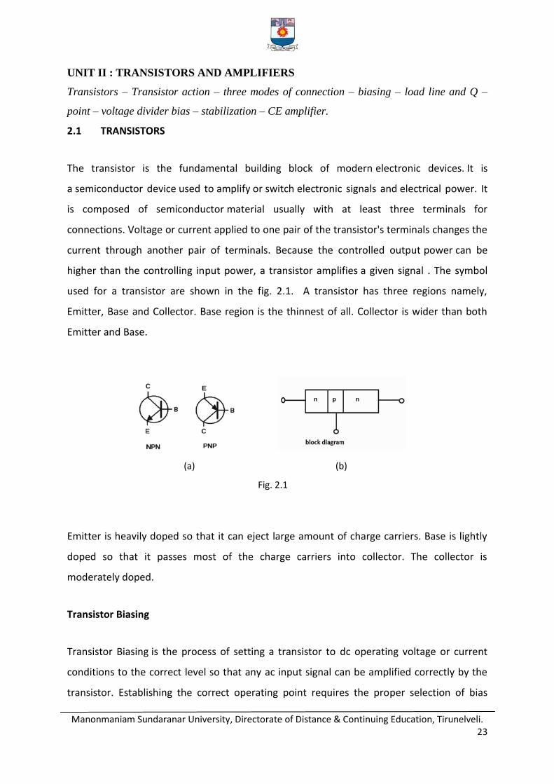
2.1 TRANSISTORS
The transistor is the fundamental building block of modern electronic devices. It is
a semiconductor device used to amplify or switch electronic signals and electrical power. It
is composed of semiconductor material usually with at least three terminals for
connections. Voltage or current applied to one pair of the transistor's terminals changes the
current through another pair of terminals. Because the controlled output power can be
higher than the controlling input power, a transistor amplifies a given signal . The symbol
used for a transistor are shown in the fig. 2.1. A transistor has three regions namely,
Emitter, Base and Collector. Base region is the thinnest of all. Collector is wider than both
Emitter and Base.
(a) (b)
Fig. 2.1
Emitter is heavily doped so that it can eject large amount of charge carriers. Base is lightly
doped so that it passes most of the charge carriers into collector. The collector is
moderately doped.
Transistor Biasing
Transistor Biasing is the process of setting a transistor to dc operating voltage or current
conditions to the correct level so that any ac input signal can be amplified correctly by the
transistor. Establishing the correct operating point requires the proper selection of bias
Manonmaniam Sundaranar University, Directorate of Distance & Continuing Education, Tirunelveli. 24
resistors and load resistors to provide the appropriate input current and collector voltage
conditions. The correct biasing point for a bipolar transistor, either npn or pnp, generally lies
somewhere between the two extremes of operation with respect to it being either “fully-
ON” or “fully-OFF” along its load line. This central operating point is called the Quiescent
Operating Point, or Q-point for short. With a single resistor usage, the biasing voltages and
currents do not remain stable during transistor operation and can vary enormously. Also the
temperature of the transistor can adversely affect the operating point.
2.2 Bias Stabilisation
It should be ensured that the operating point of a transistor is fixed at a suitable point. If it is
shifted then the transistor will be driven to undesired regions and the circuit will become
unreliable. The following are the reasons for the shift of operating point.
i. Variation of transistor parameters with temperature
ii. Parameter change from one transistor to another.
Collector current produces heat at base-collector junction. This will increase the number of
minority charge carriers at the reverse biased B-C junction and the leakage current
increases. This inturn will increase the collector current. The cycle repeats again. So, the
transistor will reach the saturation region. The excess heat produced sometimes damage
the transistor. This situation is called thermal runaway.
Stability factor
Stability factor is defined as the rate of change of collector current with respect to collector
leakage current keeping the current gain β and base current IB constant.
ie. Stability factor
BIco
C
dI
dIS
,
(2.1)
where coI is the collector leakage current.
2.3 Expression for Stability factor for C.E. configuration:
In C. E. configuration,
Manonmaniam Sundaranar University, Directorate of Distance & Continuing Education, Tirunelveli. 25
Collector current coc III B )1(
Differentiating w.r.t. cI , we can write
cc dI
dI
dI
dI coB )1(1
But stability factor
BIco
C
dI
dIS
,
SdI
dI
c
B 1)1(1
c
B
c
B
dI
dISor
dI
dI
Sor
1
1
11
)1(
(2.2)
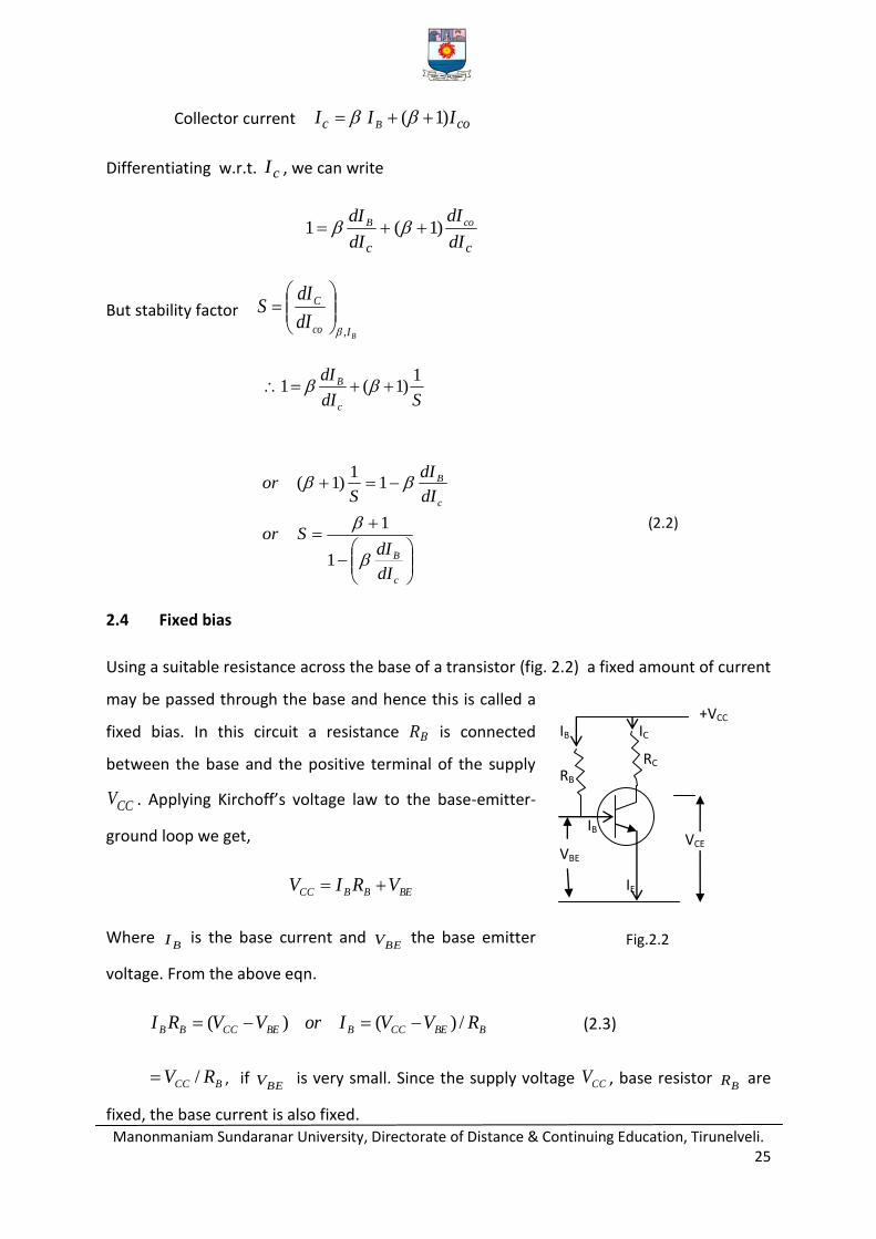
2.4 Fixed bias
Using a suitable resistance across the base of a transistor (fig. 2.2) a fixed amount of current
may be passed through the base and hence this is called a
fixed bias. In this circuit a resistance 𝑅𝐵 is connected
between the base and the positive terminal of the supply
CCV . Applying Kirchoff’s voltage law to the base-emitter-
ground loop we get,
BEBBCC VRIV
Where BI is the base current and
BEV the base emitter
voltage. From the above eqn.
BBECCBBECCBB RVVIorVVRI /)()( (2.3)
BCC RV / , if BEV is very small. Since the supply voltage CCV , base resistor
BR are
fixed, the base current is also fixed.
RB
RC
VCE VBE
+VCC
IE
IB
IB IC
Fig.2.2
Manonmaniam Sundaranar University, Directorate of Distance & Continuing Education, Tirunelveli. 26
Advantages
1) It a simple circuit to construct
2) The biasing conditions can be easily achieved
3) Since there is no resistance between base and emitter, no loading of the source by
the biasing current is reached
Disadvantages
1) Stability factor is high resulting in quick thermal runaway
2) Poor stabilisation
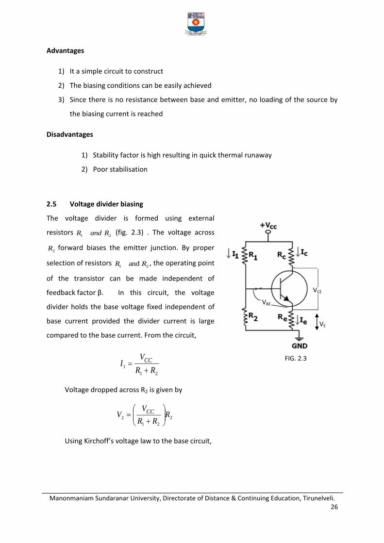
2.5 Voltage divider biasing
The voltage divider is formed using external
resistors 21 RandR (fig. 2.3) . The voltage across
2R forward biases the emitter junction. By proper
selection of resistors 21 and RR , the operating point
of the transistor can be made independent of
feedback factor β. In this circuit, the voltage
divider holds the base voltage fixed independent of
base current provided the divider current is large
compared to the base current. From the circuit,
21
1RR
VI CC
Voltage dropped across R2 is given by
2
21
2 RRR
VV CC
Using Kirchoff’s voltage law to the base circuit,
VCE
VE
VBE
FIG. 2.3
Manonmaniam Sundaranar University, Directorate of Distance & Continuing Education, Tirunelveli. 27
E
BEE
EEBE
EBE
R
VVIor
RIV
VVV
2
2
Or CIE
BE
R
VV 2 since, IE=IC
Thus, IC is independent of transistor parameters and hence good stabilisation is ensured.
This is the universal method providing transistor biasing.
Advantages of voltage divider biasing circuits
1) Only one dc supply is necessary.
2) Operating point is almost independent of β variation.
3) Operating point is stabilized against shift in temperature.
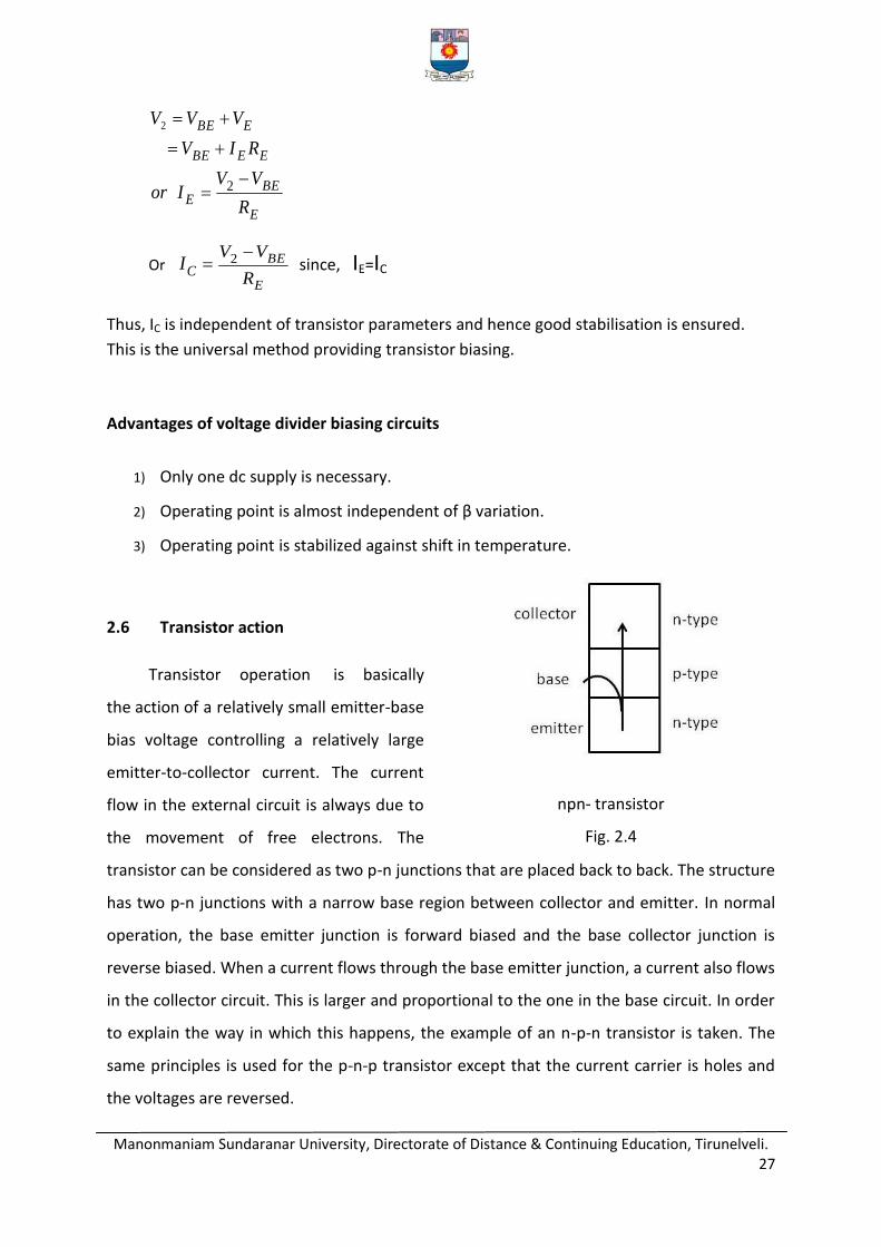
2.6 Transistor action
Transistor operation is basically
the action of a relatively small emitter-base
bias voltage controlling a relatively large
emitter-to-collector current. The current
flow in the external circuit is always due to
the movement of free electrons. The
transistor can be considered as two p-n junctions that are placed back to back. The structure
has two p-n junctions with a narrow base region between collector and emitter. In normal
operation, the base emitter junction is forward biased and the base collector junction is
reverse biased. When a current flows through the base emitter junction, a current also flows
in the collector circuit. This is larger and proportional to the one in the base circuit. In order
to explain the way in which this happens, the example of an n-p-n transistor is taken. The
same principles is used for the p-n-p transistor except that the current carrier is holes and
the voltages are reversed.
npn- transistor
Fig. 2.4
Manonmaniam Sundaranar University, Directorate of Distance & Continuing Education, Tirunelveli. 28
The emitter in the n-p-n device is made of n-type material and here the majority carriers are
electrons. When the base emitter junction is forward biased the electrons move from the n-
region towards the p- region and the holes move towards the n- region. This enables a
current to flow across the junction. When the junction is reverse biased the holes and
electrons move away from one another resulting in a depletion region between the two
areas and no current flows.
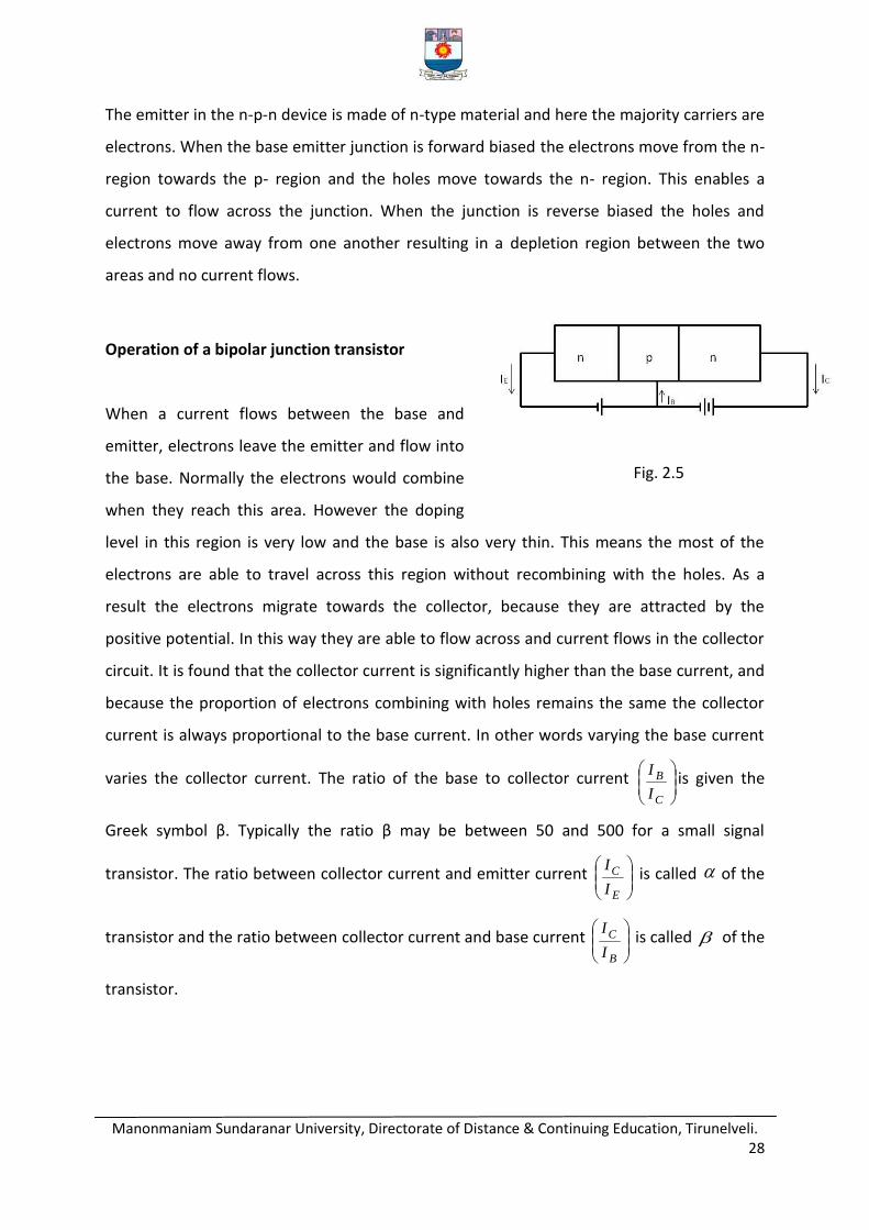
Operation of a bipolar junction transistor
When a current flows between the base and
emitter, electrons leave the emitter and flow into
the base. Normally the electrons would combine
when they reach this area. However the doping
level in this region is very low and the base is also very thin. This means the most of the
electrons are able to travel across this region without recombining with the holes. As a
result the electrons migrate towards the collector, because they are attracted by the
positive potential. In this way they are able to flow across and current flows in the collector
circuit. It is found that the collector current is significantly higher than the base current, and
because the proportion of electrons combining with holes remains the same the collector
current is always proportional to the base current. In other words varying the base current
varies the collector current. The ratio of the base to collector current
C
B
I
Iis given the
Greek symbol β. Typically the ratio β may be between 50 and 500 for a small signal
transistor. The ratio between collector current and emitter current
E
C
I
I is called of the
transistor and the ratio between collector current and base current
B
C
I
I is called of the
transistor.
Fig. 2.5
Manonmaniam Sundaranar University, Directorate of Distance & Continuing Education, Tirunelveli. 29
2.7 Relation between and of a transistor
The sum of base current and collector current is equal to the emitter current.
ie. BECCBE IIIorIII
From definition =
E
C
I
I =
E
BE
I
II
)1(
)1()1(
)(
)()(
CE
CBCE
II
IIII
cross multiplying,
111
or
11=1 (2.4)
2.8 Different modes of connections
There are three basic configurations of transistors namely, Common Base (CB), Common
Emitter (CE) and Common Collector (CC) modes used in electronic circuits. Some important
characteristics of these different modes or configurations are given below. Based on these
they are used for different applications. Figure (2.6) depicts all the three transistor
configurations used in various applications of electronic circuit.
(i) Common Base (C.B.) Mode
Common base mode (fig. 2.6a) is usually used for VHF and UHF amplifiers where, although
the voltage gain is not high, there is little chance of the output signal being fed back into the
input circuit . Because the base of the transistor is connected to ground in this mode, it
forms an effective grounded screen between output and input. As the collector current in
this mode is the emitter current minus the base current, the current gain (hfb in common
base mode) is less than unity.
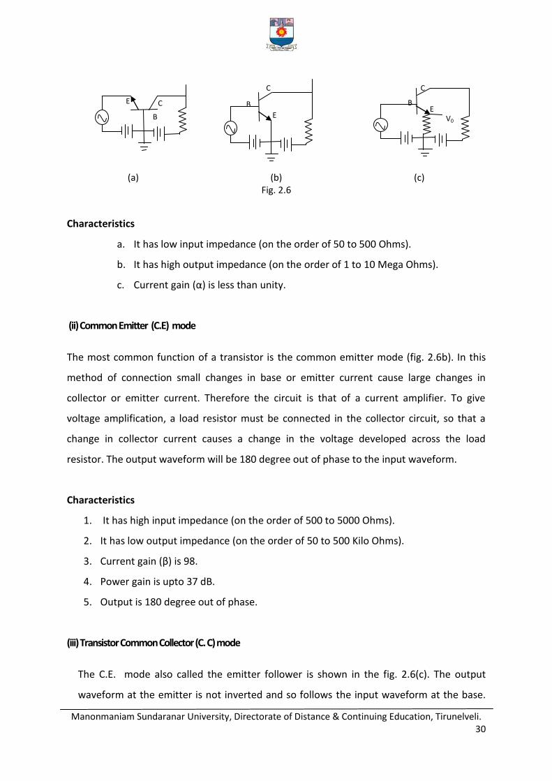
Manonmaniam Sundaranar University, Directorate of Distance & Continuing Education, Tirunelveli. 30
(a) (b) (c) Fig. 2.6
Characteristics
a. It has low input impedance (on the order of 50 to 500 Ohms).
b. It has high output impedance (on the order of 1 to 10 Mega Ohms).
c. Current gain (α) is less than unity.
(ii) Common Emitter (C.E) mode
The most common function of a transistor is the common emitter mode (fig. 2.6b). In this
method of connection small changes in base or emitter current cause large changes in
collector or emitter current. Therefore the circuit is that of a current amplifier. To give
voltage amplification, a load resistor must be connected in the collector circuit, so that a
change in collector current causes a change in the voltage developed across the load
resistor. The output waveform will be 180 degree out of phase to the input waveform.
Characteristics
1. It has high input impedance (on the order of 500 to 5000 Ohms).
2. It has low output impedance (on the order of 50 to 500 Kilo Ohms).
3. Current gain (β) is 98.
4. Power gain is upto 37 dB.
5. Output is 180 degree out of phase.
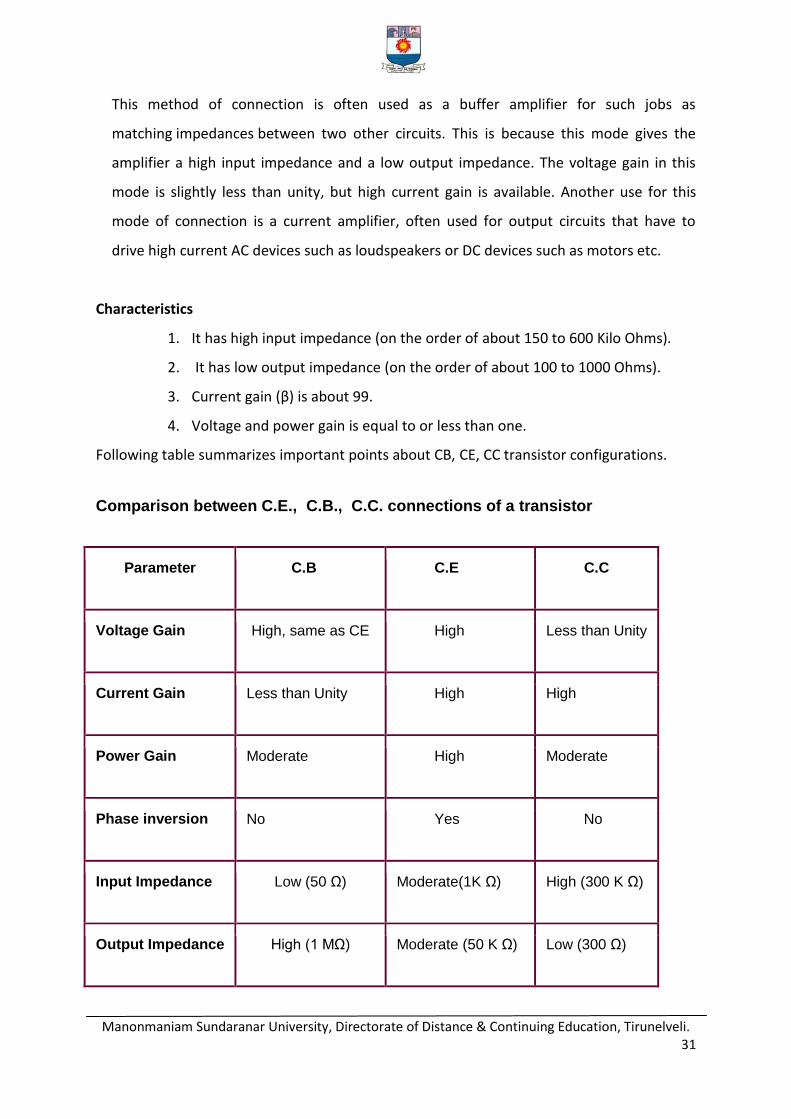
(iii) Transistor Common Collector (C. C) mode
The C.E. mode also called the emitter follower is shown in the fig. 2.6(c). The output
waveform at the emitter is not inverted and so follows the input waveform at the base.
E
B
C
V0
E B
C
E
B
C
Manonmaniam Sundaranar University, Directorate of Distance & Continuing Education, Tirunelveli. 31
This method of connection is often used as a buffer amplifier for such jobs as
matching impedances between two other circuits. This is because this mode gives the
amplifier a high input impedance and a low output impedance. The voltage gain in this
mode is slightly less than unity, but high current gain is available. Another use for this
mode of connection is a current amplifier, often used for output circuits that have to
drive high current AC devices such as loudspeakers or DC devices such as motors etc.
Characteristics
1. It has high input impedance (on the order of about 150 to 600 Kilo Ohms).
2. It has low output impedance (on the order of about 100 to 1000 Ohms).
3. Current gain (β) is about 99.
4. Voltage and power gain is equal to or less than one.
Following table summarizes important points about CB, CE, CC transistor configurations.
Comparison between C.E., C.B., C.C. connections of a transistor
Parameter C.B C.E C.C
Voltage Gain High, same as CE High Less than Unity
Current Gain Less than Unity High High
Power Gain Moderate High Moderate
Phase inversion No Yes No
Input Impedance Low (50 Ω) Moderate(1K Ω) High (300 K Ω)
Output Impedance High (1 MΩ) Moderate (50 K Ω) Low (300 Ω)
Manonmaniam Sundaranar University, Directorate of Distance & Continuing Education, Tirunelveli. 32
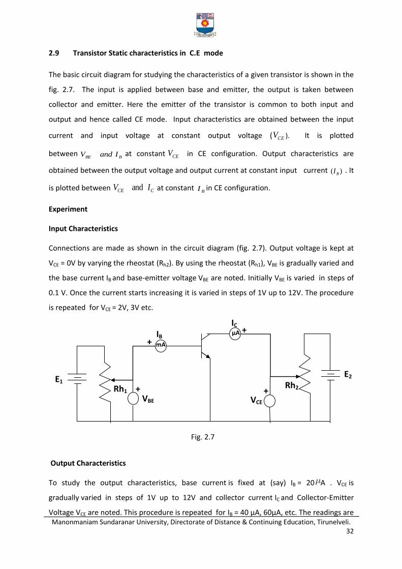
2.9 Transistor Static characteristics in C.E mode
The basic circuit diagram for studying the characteristics of a given transistor is shown in the
fig. 2.7. The input is applied between base and emitter, the output is taken between
collector and emitter. Here the emitter of the transistor is common to both input and
output and hence called CE mode. Input characteristics are obtained between the input
current and input voltage at constant output voltage ( CEV ). It is plotted
between BBE IandV at constant CEV in CE configuration. Output characteristics are
obtained between the output voltage and output current at constant input current )( BI . It
is plotted between CCE IV and at constant BI in CE configuration.
Experiment
Input Characteristics
Connections are made as shown in the circuit diagram (fig. 2.7). Output voltage is kept at
VCE = 0V by varying the rheostat (Rh2). By using the rheostat (Rh1), VBE is gradually varied and
the base current IB and base-emitter voltage VBE are noted. Initially VBE is varied in steps of
0.1 V. Once the current starts increasing it is varied in steps of 1V up to 12V. The procedure
is repeated for VCE = 2V, 3V etc.
Output Characteristics
To study the output characteristics, base current is fixed at (say) IB = 20 A . VCE is
gradually varied in steps of 1V up to 12V and collector current IC and Collector-Emitter
Voltage VCE are noted. This procedure is repeated for IB = 40 µA, 60µA, etc. The readings are
IB
IC
VBE VCE
Rh1 Rh2
E1 E2
+
+
+ +
mA
µA
Fig. 2.7
Manonmaniam Sundaranar University, Directorate of Distance & Continuing Education, Tirunelveli. 33
tabulated as shown and suitable graphs are drawn. The various parameters related are
calculated using the following formula
Input resistance
CEVB
BEi
I
Vr
Output resistance
BIC
CE
I
Vr
0
Current gain
CEVB
C
I
I
(2.5)
2.10 Quiescent Point (Q-Point)
In an amplifier to get faithful amplification, suitable bias resistance and voltage values must
be selected for the given transistor. This condition gives a set of d.c. voltage and current
values in the transistor under zero signal condition. This is known as the operating point or
Q- point. It is a point on the dc load line which represents dc collector – emitter voltage
Input Characteristics
VCE=1V VCE=2V VCE=3V
VBE(Volts) IB( µA ) VBE(Volts) IB( µA ) VBE(Volts) IB( µA )
Output Characteristics
IB=0 µA IB=20 µA IB=40 µA
VCE(Volts) Ic(mA) VCE(Volts) Ic(mA) VCE(Volts) Ic(mA)
Fig. 2.8
(a)
(b)
Manonmaniam Sundaranar University, Directorate of Distance & Continuing Education, Tirunelveli. 34
(VCE) and collector current (IC) in the absence of ac single. It is also called the operating point
because the variations in VCE and IC take place about this point when signal is applied. The
best position for this point is midway between cut-off and saturation points where VCE =
1/2 VCC. Q - Point marked on the output characteristics curve. Q-point shifts up and down
along the ac load line when changes in output voltage and current of an amplifier are
caused by an ac signal
Significance of Q - point in transistor
Normally whatever signals we want to amplify will be of the order milli volts or less. If we
directly input these signals to the amplifier they will not get amplified as transistor needs
voltages greater than cut in voltages for it to be in active region. Only in active region of
operation transistor acts as amplifier. So we can establish appropriate DC voltages and
currents through transistor by external sources so that the transistor operates in active
region and superimpose the AC signals to be amplified. The DC voltage and current are so
chosen that the transistor remains in active region for entire AC signal. All the input AC
signals variations happen around Q-point. The points where the characteristic curve and the
load line intersect are the possible operating points or Q points. To maintain the transistor
at Q value for all operating signal values, suitable biasing is done.
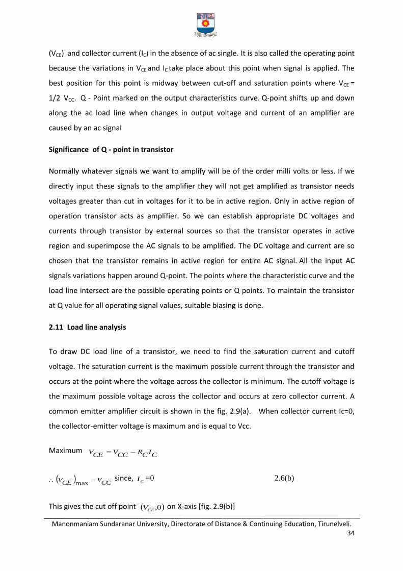
2.11 Load line analysis
To draw DC load line of a transistor, we need to find the saturation current and cutoff
voltage. The saturation current is the maximum possible current through the transistor and
occurs at the point where the voltage across the collector is minimum. The cutoff voltage is
the maximum possible voltage across the collector and occurs at zero collector current. A
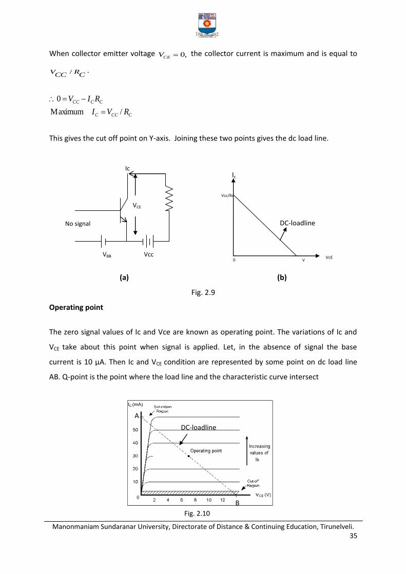
common emitter amplifier circuit is shown in the fig. 2.9(a). When collector current Ic=0,
the collector-emitter voltage is maximum and is equal to Vcc.
Maximum C
IC
RCC
VCE
V
CC
VCE
V max
since, CI =0 2.6(b)
This gives the cut off point 0,CEV on X-axis [fig. 2.9(b)]
Ic
Manonmaniam Sundaranar University, Directorate of Distance & Continuing Education, Tirunelveli. 35
When collector emitter voltage ,0CEV the collector current is maximum and is equal to
CR
CCV / .
CCCC
CCCC
RVI
RIV
/Maximum
0
This gives the cut off point on Y-axis. Joining these two points gives the dc load line.
Operating point
The zero signal values of Ic and Vce are known as operating point. The variations of Ic and
VCE take about this point when signal is applied. Let, in the absence of signal the base
current is 10 µA. Then Ic and VCE condition are represented by some point on dc load line
AB. Q-point is the point where the load line and the characteristic curve intersect
(a) (b)
Fig. 2.9
No signal
VBB Vcc
VCE
Ic
V
cc
0
Vcc/Rc
DC-loadline
Ic
VcE
DC-loadline
A
B
Fig. 2.10
Manonmaniam Sundaranar University, Directorate of Distance & Continuing Education, Tirunelveli. 36
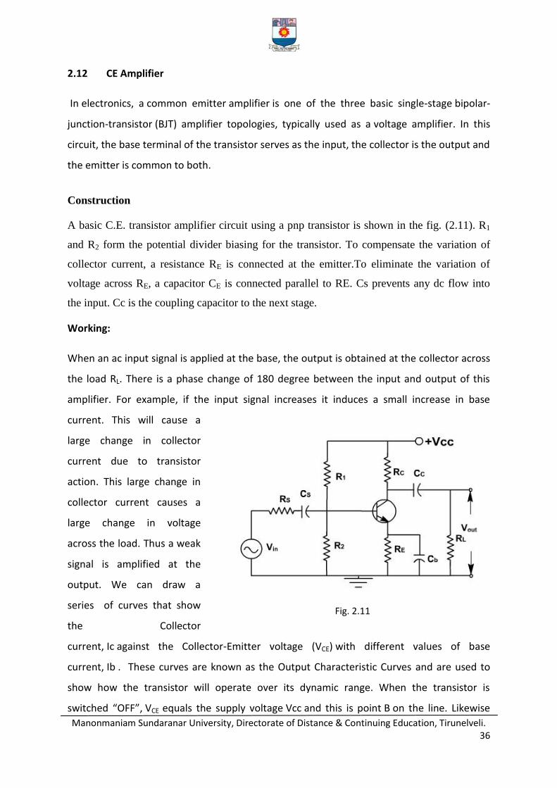
2.12 CE Amplifier
In electronics, a common emitter amplifier is one of the three basic single-stage bipolar-
junction-transistor (BJT) amplifier topologies, typically used as a voltage amplifier. In this
circuit, the base terminal of the transistor serves as the input, the collector is the output and
the emitter is common to both.
Construction
A basic C.E. transistor amplifier circuit using a pnp transistor is shown in the fig. (2.11). R1
and R2 form the potential divider biasing for the transistor. To compensate the variation of
collector current, a resistance RE is connected at the emitter.To eliminate the variation of
voltage across RE, a capacitor CE is connected parallel to RE. Cs prevents any dc flow into
the input. Cc is the coupling capacitor to the next stage.
Working:
When an ac input signal is applied at the base, the output is obtained at the collector across
the load RL. There is a phase change of 180 degree between the input and output of this
amplifier. For example, if the input signal increases it induces a small increase in base
current. This will cause a
large change in collector
current due to transistor
action. This large change in
collector current causes a
large change in voltage
across the load. Thus a weak
signal is amplified at the
output. We can draw a
series of curves that show
the Collector
current, Ic against the Collector-Emitter voltage (VCE) with different values of base
current, Ib . These curves are known as the Output Characteristic Curves and are used to
show how the transistor will operate over its dynamic range. When the transistor is
switched “OFF”, VCE equals the supply voltage Vcc and this is point B on the line. Likewise
Fig. 2.11
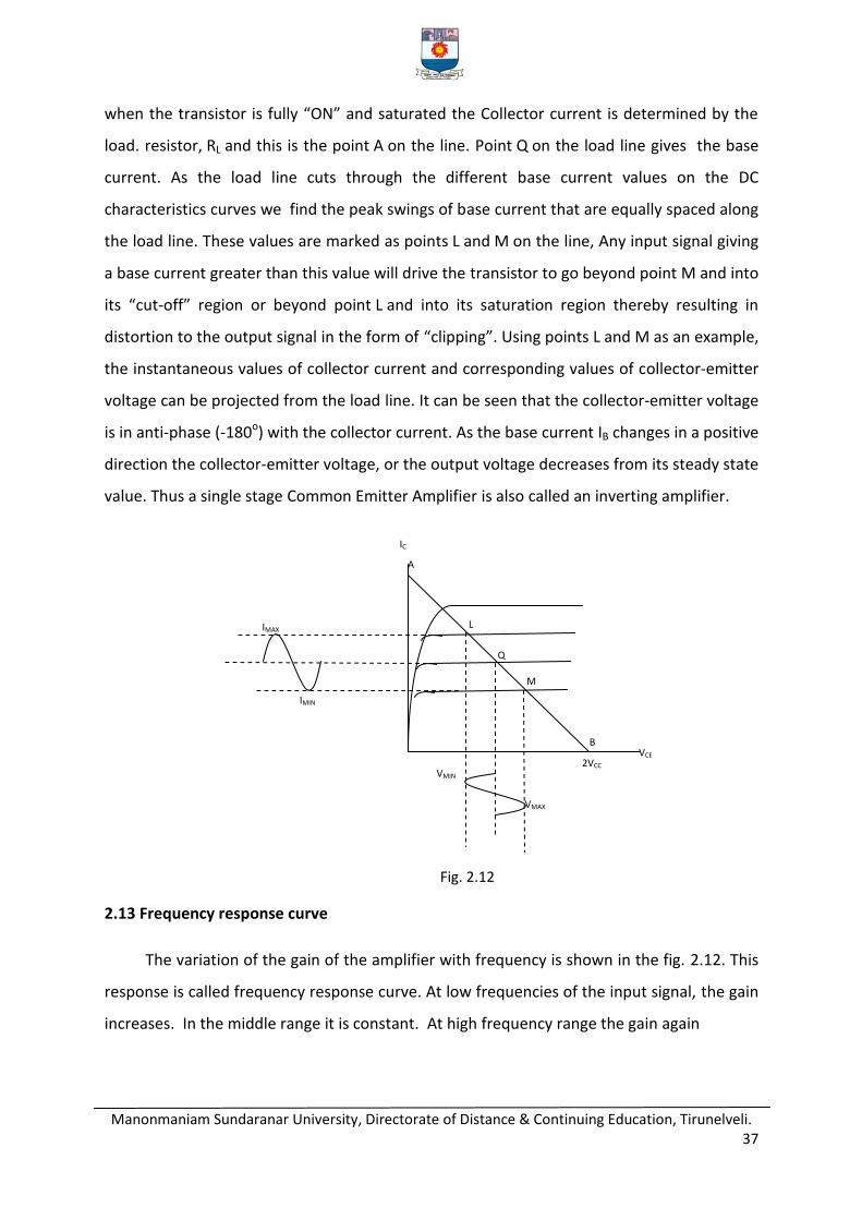
Manonmaniam Sundaranar University, Directorate of Distance & Continuing Education, Tirunelveli. 37
when the transistor is fully “ON” and saturated the Collector current is determined by the
load. resistor, RL and this is the point A on the line. Point Q on the load line gives the base
current. As the load line cuts through the different base current values on the DC
characteristics curves we find the peak swings of base current that are equally spaced along
the load line. These values are marked as points L and M on the line, Any input signal giving
a base current greater than this value will drive the transistor to go beyond point M and into
its “cut-off” region or beyond point L and into its saturation region thereby resulting in
distortion to the output signal in the form of “clipping”. Using points L and M as an example,
the instantaneous values of collector current and corresponding values of collector-emitter
voltage can be projected from the load line. It can be seen that the collector-emitter voltage
is in anti-phase (-180o) with the collector current. As the base current IB changes in a positive
direction the collector-emitter voltage, or the output voltage decreases from its steady state
value. Thus a single stage Common Emitter Amplifier is also called an inverting amplifier.
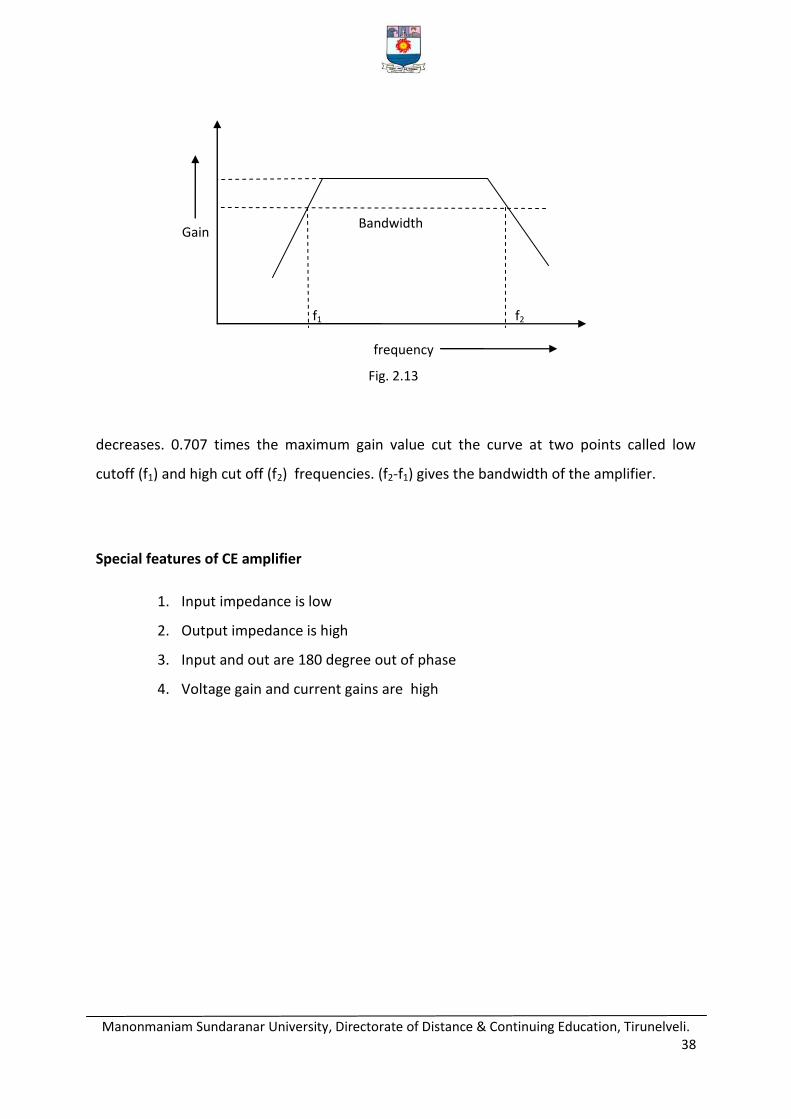
2.13 Frequency response curve
The variation of the gain of the amplifier with frequency is shown in the fig. 2.12. This
response is called frequency response curve. At low frequencies of the input signal, the gain
increases. In the middle range it is constant. At high frequency range the gain again
Q
L
M
A
B VCE
IMAX
2VCC
IC
IMIN
VMIN
VMAX
Fig. 2.12
Manonmaniam Sundaranar University, Directorate of Distance & Continuing Education, Tirunelveli. 38
decreases. 0.707 times the maximum gain value cut the curve at two points called low
cutoff (f1) and high cut off (f2) frequencies. (f2-f1) gives the bandwidth of the amplifier.
Special features of CE amplifier
1. Input impedance is low
2. Output impedance is high
3. Input and out are 180 degree out of phase
4. Voltage gain and current gains are high
f1 f2
Gain
frequency
Bandwidth
Fig. 2.13
Manonmaniam Sundaranar University, Directorate of Distance & Continuing Education, Tirunelveli. 39
UNIT III : OSCILLATORS
Principles of negative voltage feed back in amplifiers – gain – advantages – principle of
negative current feedback – Oscillation – Bark Hausen criterion for oscillation – colpitt’s
oscillator
3.1 Feedback Circuits
Feedback loops are used to control the output of electronic circuits. A feedback loop is
created when all or some portion of the output is fedback to the input. There are two types
of feedback circuits. They are positive feedback circuits and negative feedback circuits.
(i) Negative feedback
A negative feedback circuit is an electronic circuit that subtracts a fraction of its output
from its input, so that it opposes the original signal. The applied negative feedback improves
the performance by the ways of gain stability, linearity, frequency response, step response
and reduces sensitivity to parameter variations due to manufacturing or environment.
Because of these advantages, many amplifiers and control systems use negative feedback.
(ii) Positive feedback
When the feedback energy which may be voltage or current, is in phase with the input
signal then it is called positive feedback. In this case, both amplifier and the feedback circuit
introduce each a phase shift of 1800. The net result is 3600 phase shift around the loop.
3.2 Effect of negative feed back
Let V0 be the output voltage and Vi is the input voltage of an amplifier.
Then the gain of the amplifier is iV
VA 0 . (3.1)
Now using a feedback network, let a fraction of the output (β) is fedback to the input.
Now the total input voltage is 0VVV si (3.2)
From eqn 3.1, A
V
iVoriAVV 00
Manonmaniam Sundaranar University, Directorate of Distance & Continuing Education, Tirunelveli. 40
Substituting this in eqn. ( 3.2), we get
A
AA
V
V
AVAV
VAAVV
VVA
V
S
S
S
S
1'
)1(
0
0
00
00
(3.3)
This gives the gain of the amplifier with feedback.
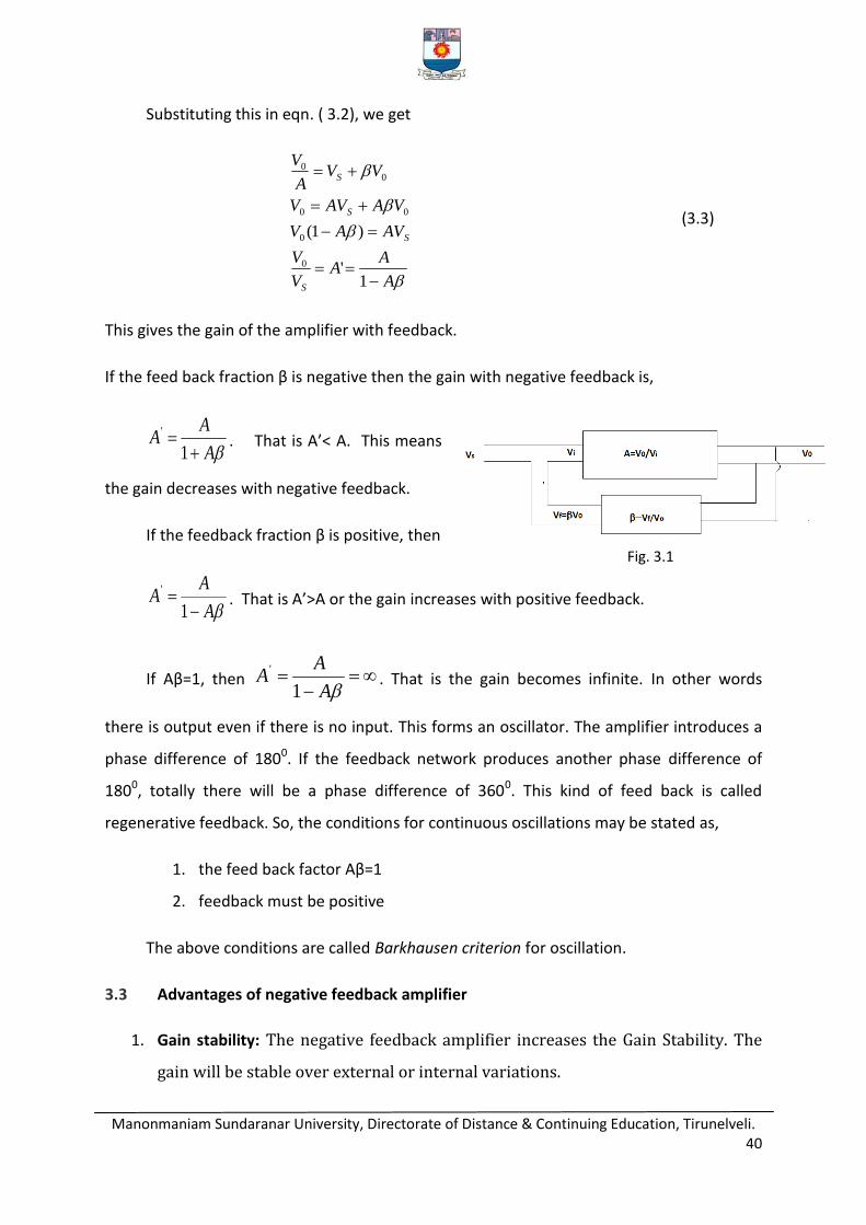
If the feed back fraction β is negative then the gain with negative feedback is,
A
AA
1
'. That is A’< A. This means
the gain decreases with negative feedback.
If the feedback fraction β is positive, then
A
AA
1
'. That is A’>A or the gain increases with positive feedback.
If Aβ=1, then
A
AA
1
'. That is the gain becomes infinite. In other words
there is output even if there is no input. This forms an oscillator. The amplifier introduces a
phase difference of 1800. If the feedback network produces another phase difference of
1800, totally there will be a phase difference of 3600. This kind of feed back is called
regenerative feedback. So, the conditions for continuous oscillations may be stated as,
1. the feed back factor Aβ=1
2. feedback must be positive
The above conditions are called Barkhausen criterion for oscillation.
3.3 Advantages of negative feedback amplifier
1. Gain stability: The negative feedback amplifier increases the Gain Stability. The
gain will be stable over external or internal variations.
Fig. 3.1
Manonmaniam Sundaranar University, Directorate of Distance & Continuing Education, Tirunelveli. 41
2. Noise reduction: By using negative feedback amplifier we can reduce the noise level
to some extent
3. Increase of Bandwidth: Negative feedback amplifier decreases the Voltage gain,
the reduction in voltage gain results improved Frequency Band Width.
4. Increase in input impedence: The amplifier with negative feedback Increases the
Input impedence. Thus we can avoid loading of signal source.
5. Decrease in output impedence: Negative feedback decreases its output impedence
Problem: The gain of an amplifier is 120. When negative voltage feedback is applied, the
gain is reduced to 20. Find the feedback ratio?
Given: ?;20';120 AA
We know that the gain of an amplifier with negative feedback is A
AA
1'
Substituting the values,
1201
12020
or 120240020
Or 24
1
2400
100 .
So, the feedback ratio=24
1
3.4 Effect of negative feedback on the stability of an amplifier
Eventhough the negative feedback reduces the gain of an amplifier, it increases the stability.
Consider an amplifier with negative feedback. Its closed loop gain is given by
Manonmaniam Sundaranar University, Directorate of Distance & Continuing Education, Tirunelveli. 42
A
AA
1' (3.4)
If feedback fraction β is very large, then we can assume AA 1
From eqn. (3.4),
1
1'
A
A
A
AA (3.5)
So the gain is depending only on the feedback fraction β, which depends on feedback
network, and is independent of any other amplifier parameters. Thus negative feedback
improves the stability of the amplifier.
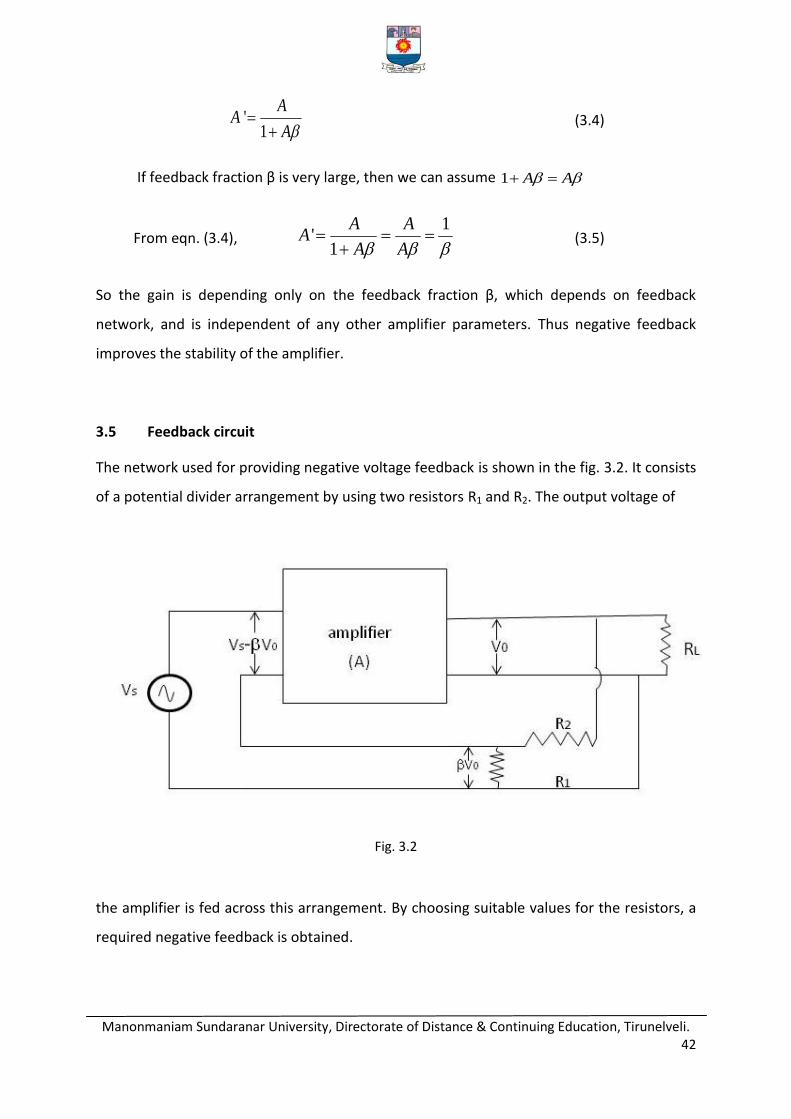
3.5 Feedback circuit
The network used for providing negative voltage feedback is shown in the fig. 3.2. It consists
of a potential divider arrangement by using two resistors R1 and R2. The output voltage of
Fig. 3.2
the amplifier is fed across this arrangement. By choosing suitable values for the resistors, a
required negative feedback is obtained.
Manonmaniam Sundaranar University, Directorate of Distance & Continuing Education, Tirunelveli. 43
From the circuit, voltage across 1
21
0
1 RRR
VR
Feedback fraction 21
1
0
1acrossvoltage
RR
R
V
R
(3.6)
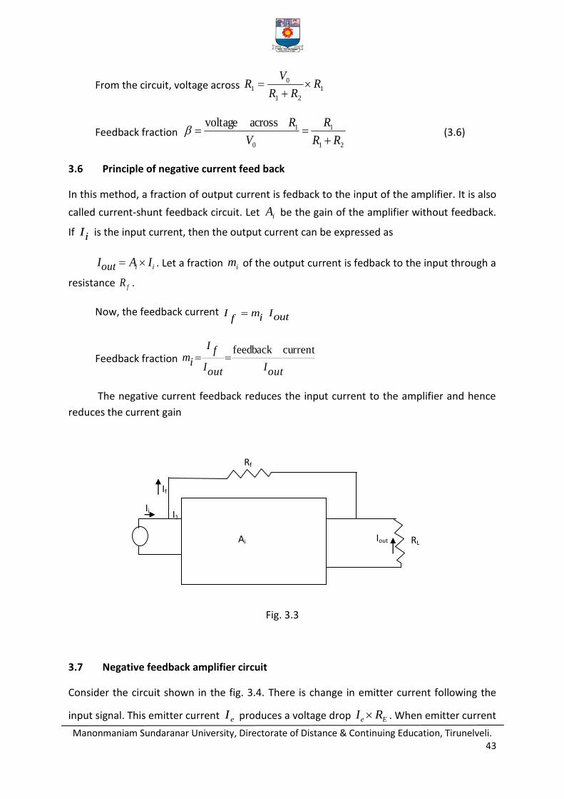
3.6 Principle of negative current feed back
In this method, a fraction of output current is fedback to the input of the amplifier. It is also
called current-shunt feedback circuit. Let iA be the gain of the amplifier without feedback.
If iI is the input current, then the output current can be expressed as
ii IAIout . Let a fraction im of the output current is fedback to the input through a
resistance fR .
Now, the feedback current outIim
fI
Feedback fraction outIoutI
fI
imcurrentfeedback
The negative current feedback reduces the input current to the amplifier and hence
reduces the current gain
3.7 Negative feedback amplifier circuit
Consider the circuit shown in the fig. 3.4. There is change in emitter current following the
input signal. This emitter current eI produces a voltage drop Ee RI . When emitter current
Fig. 3.3
Ii
If
I1
Iout RL Ai
Rf
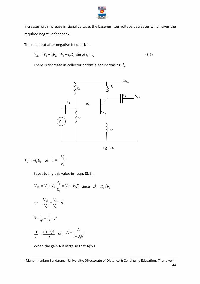
Manonmaniam Sundaranar University, Directorate of Distance & Continuing Education, Tirunelveli. 44
increases with increase in signal voltage, the base-emitter voltage decreases which gives the
required negative feedback
The net input after negative feedback is
ceEcsEesBE iiceRiVRiVV sin, (3.7)
There is decrease in collector potential for increasing cI
ccRiV 0 or c
cR
Vi 0
Substituting this value in eqn. (3.5),
00 VVR
RVVV s
c
EsBE since cE RR
Or 00 V
V
V
V sBE
ie. AA
1
'
1
A
A
A
1
'
1 or A
AA
1'
When the gain A is large so that Aβ>1
R3
C2
R2
Vin
RE
R1 RC
C1
Vout
+Vcc
Fig. 3.4
Manonmaniam Sundaranar University, Directorate of Distance & Continuing Education, Tirunelveli. 45
1'
A
AA
The closed loop gain of the negative feedback amplifier is
ERcRA '
Problem: An amplifier has a gain of 100 without feedback. If a negative feed back
with feedback ratio of 0.1 is applied, find the new gain of the amplifier?
We know that, the gain of an amplifier with negative feedback is
A
AA
1
'. Here, 1.0100 andA
Gain with feedback
09.911
100
101
100
1.01001
100
1
'
A
AA
So, the new gain with feedback= 9.09
An amplifier has a gain of 100 without feedback. When negative feedback is applied
the gain is reduced to 50. Find the feedback fraction.
Given: ?;50';100 AA
We know that the gain with negative feedback is A
AA
1'
Ie.
01.050100
50100
'
'
''
1'
AA
AA
AAAA
AAA
3.8 Emitter Follower (Negative current feedback circuit)
The circuit shown in fig. 3.5 is the emitter follower circuit or common collector amplifier
circuit. The ac voltage Vin is coupled into the base of the transistor through the coupling
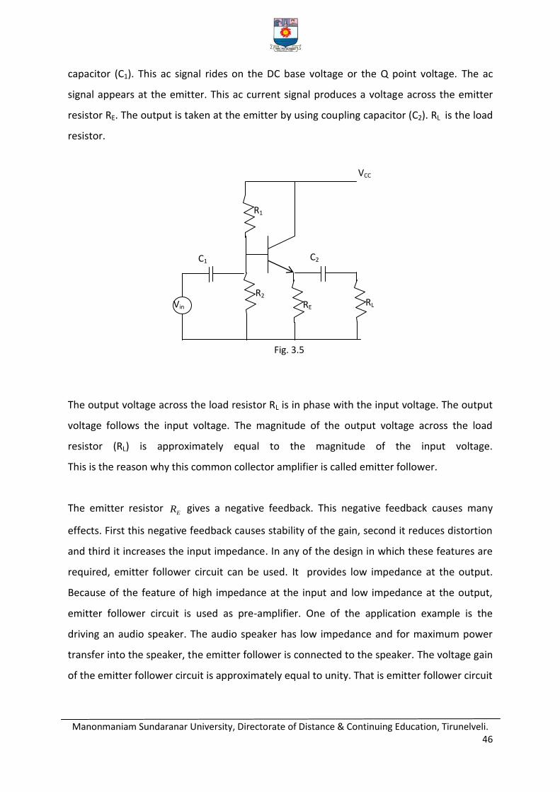
Manonmaniam Sundaranar University, Directorate of Distance & Continuing Education, Tirunelveli. 46
capacitor (C1). This ac signal rides on the DC base voltage or the Q point voltage. The ac
signal appears at the emitter. This ac current signal produces a voltage across the emitter
resistor RE. The output is taken at the emitter by using coupling capacitor (C2). RL is the load
resistor.
The output voltage across the load resistor RL is in phase with the input voltage. The output
voltage follows the input voltage. The magnitude of the output voltage across the load
resistor (RL) is approximately equal to the magnitude of the input voltage.
This is the reason why this common collector amplifier is called emitter follower.
The emitter resistor ER gives a negative feedback. This negative feedback causes many
effects. First this negative feedback causes stability of the gain, second it reduces distortion
and third it increases the input impedance. In any of the design in which these features are
required, emitter follower circuit can be used. It provides low impedance at the output.
Because of the feature of high impedance at the input and low impedance at the output,
emitter follower circuit is used as pre-amplifier. One of the application example is the
driving an audio speaker. The audio speaker has low impedance and for maximum power
transfer into the speaker, the emitter follower is connected to the speaker. The voltage gain
of the emitter follower circuit is approximately equal to unity. That is emitter follower circuit
R1
R2
RE RL
VCC
C1 C2
Vin
Fig. 3.5
Manonmaniam Sundaranar University, Directorate of Distance & Continuing Education, Tirunelveli. 47
does not provide voltage gain. However it provides current gain and thereof power gain.
Thus because of this current gain and power gain emitter follower is called an amplifier.
3.9 Oscillator
An electronic oscillator is a circuit that produces a periodic, oscillating electronic signal,
often a sine wave or a square wave. Oscillators convert direct current (DC) from a power
supply to an alternating current (AC) signal. They are widely used in many electronic
devices. Common examples of signals generated by oscillators include signals broadcast
by radio and television transmitters, clock signals that regulate computers and quartz clocks,
and the sound produced by electronic beepers and video games.
Oscillators are characterized by the frequency generated at the output. They are,
i. A low-frequency oscillator (LFO) is an electronic oscillator that generates a frequency
below 20 Hz. This is used in the field of audio synthesizers, to distinguish it from an
audio frequency oscillator.
ii. An audio oscillator produces frequencies in the audio range, about 20 Hz to 20 KHz.
iii. An RF oscillator produces signals in the radio frequency (RF) range of about 100 KHz
to 100 GH
3.10 Essential requirements for an oscillator
1) Amplifier: which receives dc power from a dC source and convert it into ac power
2) Tank circuit: which consists of an inductor (L) and a capacitor (C) connected parallel to each
other. The resonance frequency depends upon the values of L and C
3) Feedback circuit: A network providing a feedback of a fraction of the output back into the
input. The feedback must be positive such that the feedback signal is in phase with the input
signal.
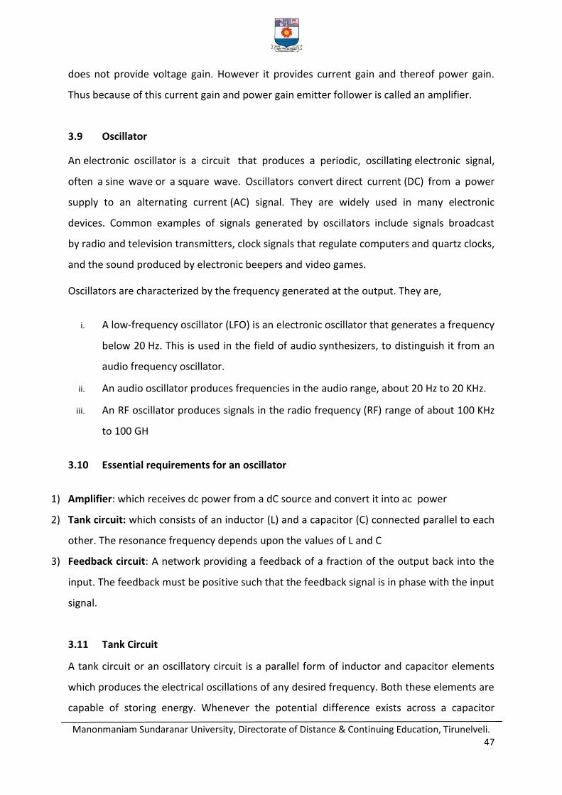
3.11 Tank Circuit
A tank circuit or an oscillatory circuit is a parallel form of inductor and capacitor elements
which produces the electrical oscillations of any desired frequency. Both these elements are
capable of storing energy. Whenever the potential difference exists across a capacitor
Manonmaniam Sundaranar University, Directorate of Distance & Continuing Education, Tirunelveli. 48
plates, it stores energy in its electric field. Similarly, whenever current flows thorough an
inductor, energy is stored in its magnetic field. The figure 3.6 shows a tank circuit in which
inductor L and capacitor C are connected in parallel.
Let us consider that the capacitor is initially charged with a DC source having the polarities
upper plate positive and lower plate negative as shown (fig. 3.6). This represents that the
upper plate has of electrons deficiency , whereas the lower plate has excess of electrons.
Therefore, potential differences exist between these two plates. Consider that this charged
capacitor is connected across the inductor. The conventional current flow from positive
polarity to negative polarity through the inductor coil. Therefore the energy stored or
strength of the electric field in the capacitor decreases. The current flowing through the
inductor induces an e.m.f. which opposes the electrons flow through it. This current flow set
up a magnetic field around the inductor thereby it starts storing the magnetic energy. When
the capacitor is fully discharged, current through the coil becomes zero. At this time
magnetic field has maximum value and there is no electric field. Thus the electrical energy is
converted into magnetic energy.
Once the capacitor is fully discharged, magnetic field around the inductor starts collapsing
and produces the counter e.m.f. As per the Lenz’s law, this counter e.m.f. produces the
current which begin to charge the capacitor with opposite polarity by making plate upper
plate negative and lower plate positive as shown in figure. When the capacitor is fully
charged in opposite direction, the entire magnetic energy is converted back into the electric
energy in capacitor, i.e., magnetic energy is collapsed. At this instant, capacitor starts
discharging in the opposite direction. Once again the capacitor is fully discharged and this
process will be continued. This continuous charging and discharging process results in an
alternating motion of electrons which is nothing but an oscillating current.
+
+
FIG. 3.6
Manonmaniam Sundaranar University, Directorate of Distance & Continuing Education, Tirunelveli. 49
3.12 Feedback oscillator
The most common form of linear oscillator is an electronic amplifier such as
a transistor or operational amplifier connected in a feedback loop with its output fed back
into its input through a frequency selective electronic filter to provide positive feedback.
When the power supply to the amplifier is first switched on, electronic noise in the circuit
provides a non-zero signal to get oscillations started. The noise travels around the loop and
is amplified. Feedback oscillator circuits can be classified according to the type of frequency
selective filter they use in the feedback loop.
In an RC oscillator circuit, the filter is a network of resistors and capacitors. RC oscillators
are mostly used to generate lower frequencies, for example in the audio range. Common
types of RC oscillator circuits are the phase shift oscillator and the Wien bridge oscillator.
In an LC oscillator circuit, the filter is a tuned circuit , called a tank circuit consisting of
an inductor (L) and capacitor (C) connected parallel to each other. Charge flows back and
forth between the capacitor's plates through the inductor, so the tuned circuit can store
electrical energy oscillating at its resonant frequency. There are small losses in the tank
circuit, but the amplifier compensates for those losses and supplies the power for the
output signal. LC oscillators are often used at radio frequencies when a tunable frequency
source is necessary, such as in signal generators, tunable radio transmitters and the local
oscillators in radio receivers. Typical LC oscillator circuits are the Hartley, Colpitts and
Clapp circuits
In a crystal oscillator circuit the filter is a piezoelectric crystal (commonly a quartz crystal).
The crystal mechanically vibrates as a resonator, and its frequency of vibration determines
the oscillation frequency. Crystals have very high Q-factor and also better temperature
stability than tuned circuits, so crystal oscillators have much better frequency stability than
LC or RC oscillators. Crystal oscillators are the most common type of linear oscillator, used to
stabilize the frequency of most radio transmitters, and to generate the clock signal in
computers and quartz clocks. Crystal oscillators often use the same circuits as LC oscillators,
with the crystal replacing the tuned circuit. Quartz crystals are generally limited to
frequencies of 30 MHz or below. Other types of resonator, dielectric resonators and surface
Manonmaniam Sundaranar University, Directorate of Distance & Continuing Education, Tirunelveli. 50
acoustic wave (SAW) devices, are used to control higher frequency oscillators, up into
the microwave range. For example, SAW oscillators are used to generate the radio signal
in cell phones.
3.13 Colpitts Oscillator
Colpitts oscillator was invented by American scientist Edwin Colpitts in 1918. It is another
type of sinusoidal LC oscillator. In Colpitts oscillator the tank circuit consists of two
capacitors in series and an inductor connected in parallel to the serial combination. The
frequency of the oscillations are determined by the value of the capcitors and inductor in
the tank circuit. In Colpitts oscillator, the capacitive voltage divider setup in the tank circuit
works as the feed back source and this arrangement gives better frequency stability when
compared to the Hartley oscillator which uses an inductive voltage divider arrangement for
feedback. The circuit diagram of a typical Colpitts oscillator using transistor is shown in the
fig. 3.7.
In the circuit diagram resistors 1R and
2R provide a voltage divider biasing to the transistor.
Resistor CR limits the collector current of the transistor. iC is the input DC decoupling
capacitor while oC is the output decoupling capacitor. ER is the emitter resistor and its
meant for thermal stability. EC is the emitter by-pass capacitor. The emitter by-pass
capacitor is to by-pass the amplified AC signals from dropping across ER . Capacitors
1C , 2C
and inductor L form the tank circuit. Feedback to the base of transistor is taken from the
junction of Capacitor 2C and inductor L in the tank circuit.
When the power supply is switched ON, capacitors 1C and
2C start charging. When they
are fully charged they start discharging through the inductor L . When the capacitors are
fully discharged, the electrostatic energy stored in the capacitors get transferred to the
inductor as magnetic flux. The inductor starts discharging and capacitors get charged again.
This transfer of energy back and forth between capacitors and inductor is the basis of
oscillation. Voltage across 2C is phase opposite to that of the voltage across the
1C and it is
the voltage across 2C that is fed back to the transistor. The feedback signal at the base base
of transistor appears in the amplified form across the collector and emitter of the transistor.
The energy lost in the tank circuit is compensated by the transistor and the oscillations are
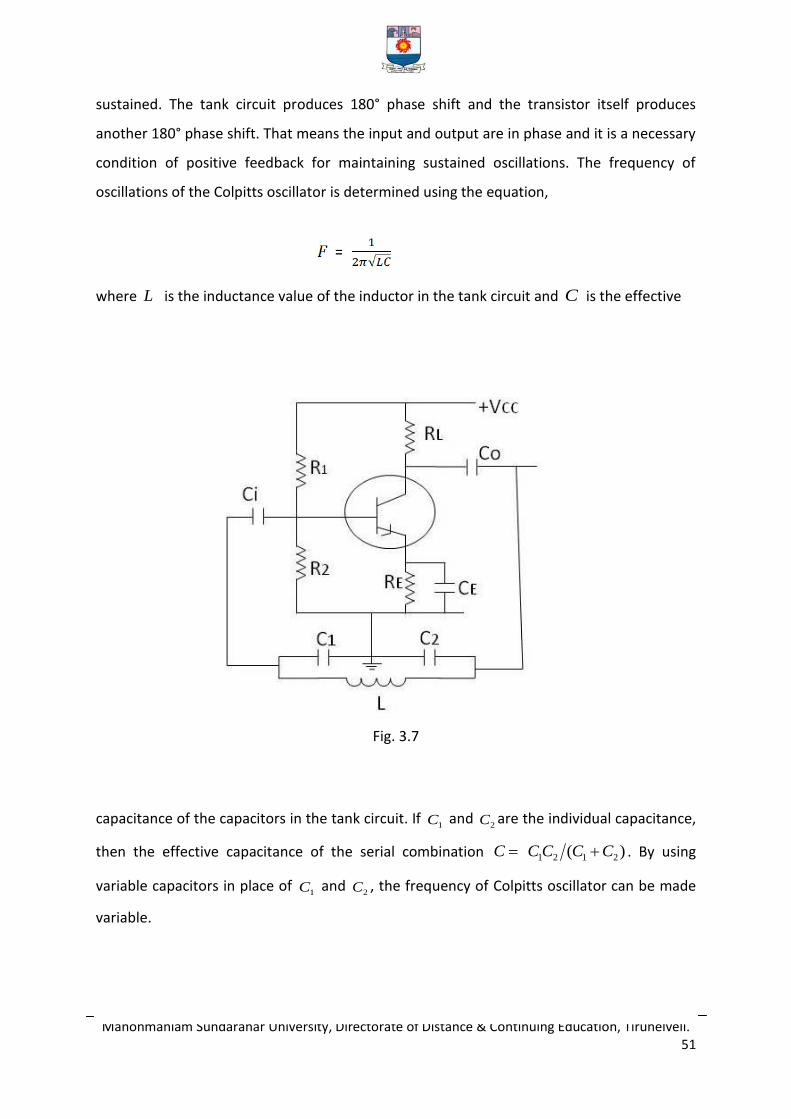
Manonmaniam Sundaranar University, Directorate of Distance & Continuing Education, Tirunelveli. 51
sustained. The tank circuit produces 180° phase shift and the transistor itself produces
another 180° phase shift. That means the input and output are in phase and it is a necessary
condition of positive feedback for maintaining sustained oscillations. The frequency of
oscillations of the Colpitts oscillator is determined using the equation,
where L is the inductance value of the inductor in the tank circuit and C is the effective
capacitance of the capacitors in the tank circuit. If 1C and
2C are the individual capacitance,
then the effective capacitance of the serial combination )( 2121 CCCCC . By using
variable capacitors in place of 1C and
2C , the frequency of Colpitts oscillator can be made
variable.
Fig. 3.7
Manonmaniam Sundaranar University, Directorate of Distance & Continuing Education, Tirunelveli. 52
3.14 Condition for oscillation
The condition for the functioning of the oscillator is 1A . In the given circuit, voltage
gain ec rRA ,where cR is the load resistance and er is the dynamic resistance of base
emitter junction.
So the condition for oscillation is
1
1
e
c
e
c
r
Ror
r
R
(3.7)
Feedback ratio β=voltageoutput
basethetofedbackvoltage=
1
2
2
1
0 /
/
C
C
Ci
Ci
V
V f
Substituting in eqn. 3.7
2
1
C
C
r
R
e
c
Or 2
1
C
Ch fe where feh =
c
C
r
R is called the forward current gain.
This is the condition for oscillation.
3.15 Expression for frequency
Resonance frequency is the oscillator frequency
At resonance, LC XX .That is
LC
1 where
21
111
CCC
Or LC
12 or LC
f1
2
Or LC
f2
1
This is the frequency of the colpitt’s oscillator.
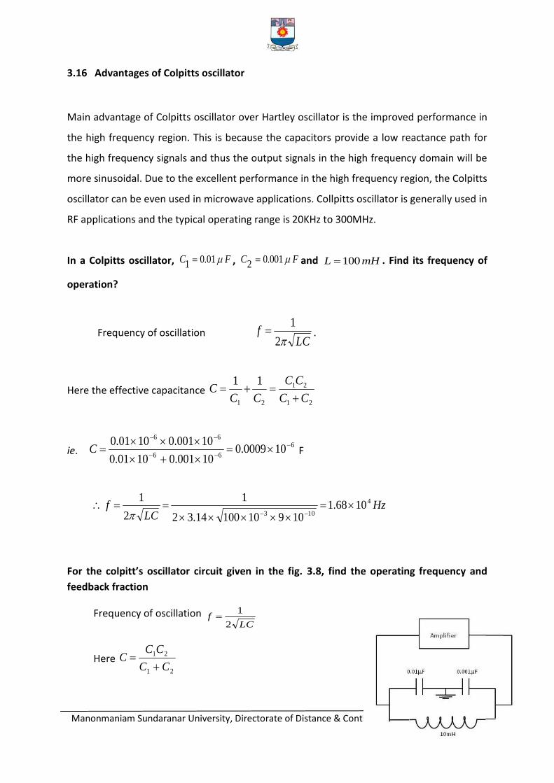
Manonmaniam Sundaranar University, Directorate of Distance & Continuing Education, Tirunelveli. 53
3.16 Advantages of Colpitts oscillator
Main advantage of Colpitts oscillator over Hartley oscillator is the improved performance in
the high frequency region. This is because the capacitors provide a low reactance path for
the high frequency signals and thus the output signals in the high frequency domain will be
more sinusoidal. Due to the excellent performance in the high frequency region, the Colpitts
oscillator can be even used in microwave applications. Collpitts oscillator is generally used in
RF applications and the typical operating range is 20KHz to 300MHz.
In a Colpitts oscillator, FC 01.01 , FC 001.02 and mHL 100 . Find its frequency of
operation?
Frequency of oscillation LC
f2
1 .
Here the effective capacitance 21
21
21
11
CC
CC
CCC
ie. 6
66
66
100009.010001.01001.0
10001.01001.0
C F
HzLC
f 4
1031068.1
1091010014.32
1
2
1
For the colpitt’s oscillator circuit given in the fig. 3.8, find the operating frequency and
feedback fraction
Frequency of oscillation LC
f2
1
Here 21
21
CC
CCC
Manonmaniam Sundaranar University, Directorate of Distance & Continuing Education, Tirunelveli. 54
In our problem,
HL 31010
FCandFC 6
2
6
1 1001.010001.0
6
66
66
100009.010001.01001.0
10001.01001.0
C
Hence, frequency of oscillation
Hz
f
53100
100009.0101014.32
1
63
Feedback fraction 10
1
01.0
001.0
2
1 C
C
Fig. 3.8
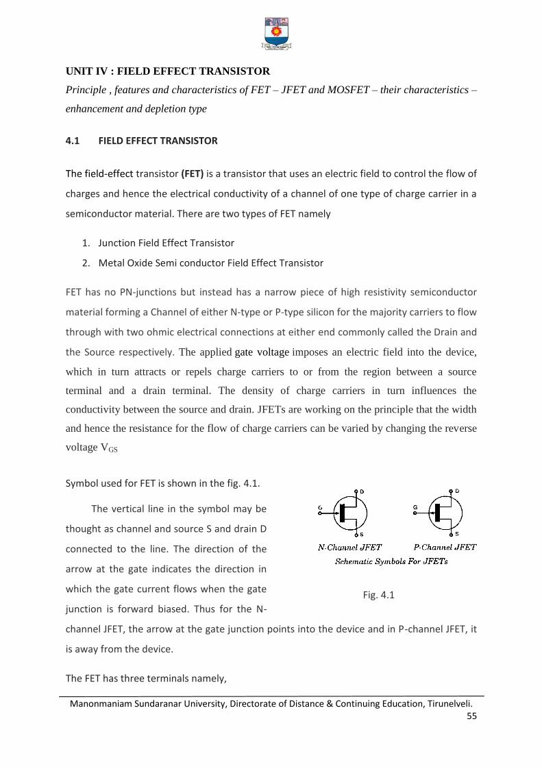
Manonmaniam Sundaranar University, Directorate of Distance & Continuing Education, Tirunelveli. 55
UNIT IV : FIELD EFFECT TRANSISTOR
Principle , features and characteristics of FET – JFET and MOSFET – their characteristics –
enhancement and depletion type
4.1 FIELD EFFECT TRANSISTOR
The field-effect transistor (FET) is a transistor that uses an electric field to control the flow of
charges and hence the electrical conductivity of a channel of one type of charge carrier in a
semiconductor material. There are two types of FET namely
1. Junction Field Effect Transistor
2. Metal Oxide Semi conductor Field Effect Transistor
FET has no PN-junctions but instead has a narrow piece of high resistivity semiconductor
material forming a Channel of either N-type or P-type silicon for the majority carriers to flow
through with two ohmic electrical connections at either end commonly called the Drain and
the Source respectively. The applied gate voltage imposes an electric field into the device,
which in turn attracts or repels charge carriers to or from the region between a source
terminal and a drain terminal. The density of charge carriers in turn influences the
conductivity between the source and drain. JFETs are working on the principle that the width
and hence the resistance for the flow of charge carriers can be varied by changing the reverse
voltage VGS
Symbol used for FET is shown in the fig. 4.1.
The vertical line in the symbol may be
thought as channel and source S and drain D
connected to the line. The direction of the
arrow at the gate indicates the direction in
which the gate current flows when the gate
junction is forward biased. Thus for the N-
channel JFET, the arrow at the gate junction points into the device and in P-channel JFET, it
is away from the device.
The FET has three terminals namely,
Fig. 4.1
Manonmaniam Sundaranar University, Directorate of Distance & Continuing Education, Tirunelveli. 56
1. Source (S), through which the carriers enter the channel. Conventionally, current
entering the channel at S is designated by IS.
2. Drain (D), through which the charge carriers leave the channel. Conventionally,
current entering the channel at D is designated by ID. Drain-to-source voltage is VDS.
3. Gate (G), is the terminal that modulates the channel conductivity. By applying
voltage to G, one can control ID.
4.2 Difference between FET and Bipolar transistor
1. In FET, only one type of charge carrier (either electrons or holes) is used for
conduction, so it is called unipolar device. In transistor, both types of charge carriers are
used for conduction, hence called a bipolar device.
2. FET has high input impedance while a transistor has low input impedance
3. Almost zero current passes through the gate of a JFET .But in a transistor, a few µA
of current pass through the base
4. FET uses gate voltage to control the output current while a transistor uses current
through the base to control the output current. Hence we can say, a FET is
characterised by its transconductance and the transistor is characterised by current
gain.
5. Noise is less in FET because there are no junctions.
4.3 Construction of FET
There are two basic configurations of field effect transistor, the N-channel JFET
(fig. 4.2 a) and the P-channel FET (4.2 b). The N-channel is doped with donor impurities
meaning that the flow of current through the channel is negative (hence the term N-
channel) in the form of electrons.
Likewise, the P-channel FET’s channel is doped with acceptor impurities meaning that
the flow of current through the channel is positive (hence the term P-channel) in the
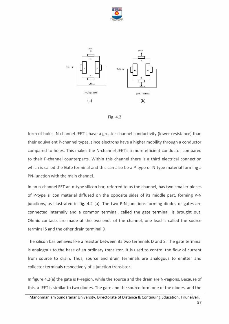
Manonmaniam Sundaranar University, Directorate of Distance & Continuing Education, Tirunelveli. 57
form of holes. N-channel JFET’s have a greater channel conductivity (lower resistance) than
their equivalent P-channel types, since electrons have a higher mobility through a conductor
compared to holes. This makes the N-channel JFET’s a more efficient conductor compared
to their P-channel counterparts. Within this channel there is a third electrical connection
which is called the Gate terminal and this can also be a P-type or N-type material forming a
PN-junction with the main channel.
In an n-channel FET an n-type silicon bar, referred to as the channel, has two smaller pieces
of P-type silicon material diffused on the opposite sides of its middle part, forming P-N
junctions, as illustrated in fig. 4.2 (a). The two P-N junctions forming diodes or gates are
connected internally and a common terminal, called the gate terminal, is brought out.
Ohmic contacts are made at the two ends of the channel, one lead is called the source
terminal S and the other drain terminal D.
The silicon bar behaves like a resistor between its two terminals D and S. The gate terminal
is analogous to the base of an ordinary transistor. It is used to control the flow of current
from source to drain. Thus, source and drain terminals are analogous to emitter and
collector terminals respectively of a junction transistor.
In figure 4.2(a) the gate is P-region, while the source and the drain are N-regions. Because of
this, a JFET is similar to two diodes. The gate and the source form one of the diodes, and the
Fig. 4.2
(a) (b)
Manonmaniam Sundaranar University, Directorate of Distance & Continuing Education, Tirunelveli. 58
drain form the other diode. These two diodes are usually referred as the gate-source diode
and the gate-drain diode. Since FET is a silicon device, it takes only 0.7 volts for forward bias
to get significant current in either diode.
With the gate terminal not connected, and a potential applied ( +ve at the drain and – ve at
the source), a current called the drain current, ID flows through the channel located
between the two P-regions. This current consists of only majority carriers-electrons in this
case. P-channel JFET is similar in construction to N-channel JFET except that P-type
semiconductor material is sandwiched between two N-type junctions, as shown in figure. In
this case majority carriers are holes.
Working
FET operation can be compared to that of a garden hose. The flow of water through a hose
can be controlled by squeezing it to reduce the cross section and the flow of electric charge
through a FET is controlled by constricting the current-carrying channel. The current also
depends on the electric field between source and drain which is analogous to the difference
in pressure on either end of the hose. Constriction of the conducting channel is
accomplished using the field effect. A voltage between the gate and the source is applied to
reverse bias the gate-source pn-junction, thereby widening the depletion layer of this
junction .
4.4 Polarity conventions FET
The polarities for n-channel and p-channel JFET’s are shown in figure. 4.3. In both of the
cases the voltage between the gate and source is such that the gate is reverse biased. This is
the normal method of connection of FETs. The drain and source terminals are penetrate
more deeply into the channel at points lying closer to D than to S. Thus wedge-shaped
depletion regions are formed, as shown in figure. when VDS is applied. The size of the
depletion layer formed determines-the width of the channel and hence the magnitude of
current ID flowing through the channel. interchangeable, that is either end can be used as a
source and the other end as a drain. The source terminal is always connected to that end of
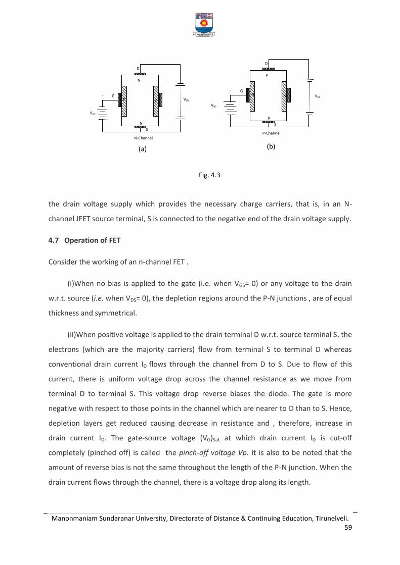
Manonmaniam Sundaranar University, Directorate of Distance & Continuing Education, Tirunelveli. 59
the drain voltage supply which provides the necessary charge carriers, that is, in an N-
channel JFET source terminal, S is connected to the negative end of the drain voltage supply.
4.7 Operation of FET
Consider the working of an n-channel FET .
(i)When no bias is applied to the gate (i.e. when VGS= 0) or any voltage to the drain
w.r.t. source (i.e. when VDS= 0), the depletion regions around the P-N junctions , are of equal
thickness and symmetrical.
(ii)When positive voltage is applied to the drain terminal D w.r.t. source terminal S, the
electrons (which are the majority carriers) flow from terminal S to terminal D whereas
conventional drain current ID flows through the channel from D to S. Due to flow of this
current, there is uniform voltage drop across the channel resistance as we move from
terminal D to terminal S. This voltage drop reverse biases the diode. The gate is more
negative with respect to those points in the channel which are nearer to D than to S. Hence,
depletion layers get reduced causing decrease in resistance and , therefore, increase in
drain current ID. The gate-source voltage (VG)Sat at which drain current ID is cut-off
completely (pinched off) is called the pinch-off voltage Vp. It is also to be noted that the
amount of reverse bias is not the same throughout the length of the P-N junction. When the
drain current flows through the channel, there is a voltage drop along its length.
D
G
S
N
N
P P VDS
VGS
N-Channel
D
G
S
P
P
N N VDS
VGS
P-Channel
(a) (b)
Fig. 4.3
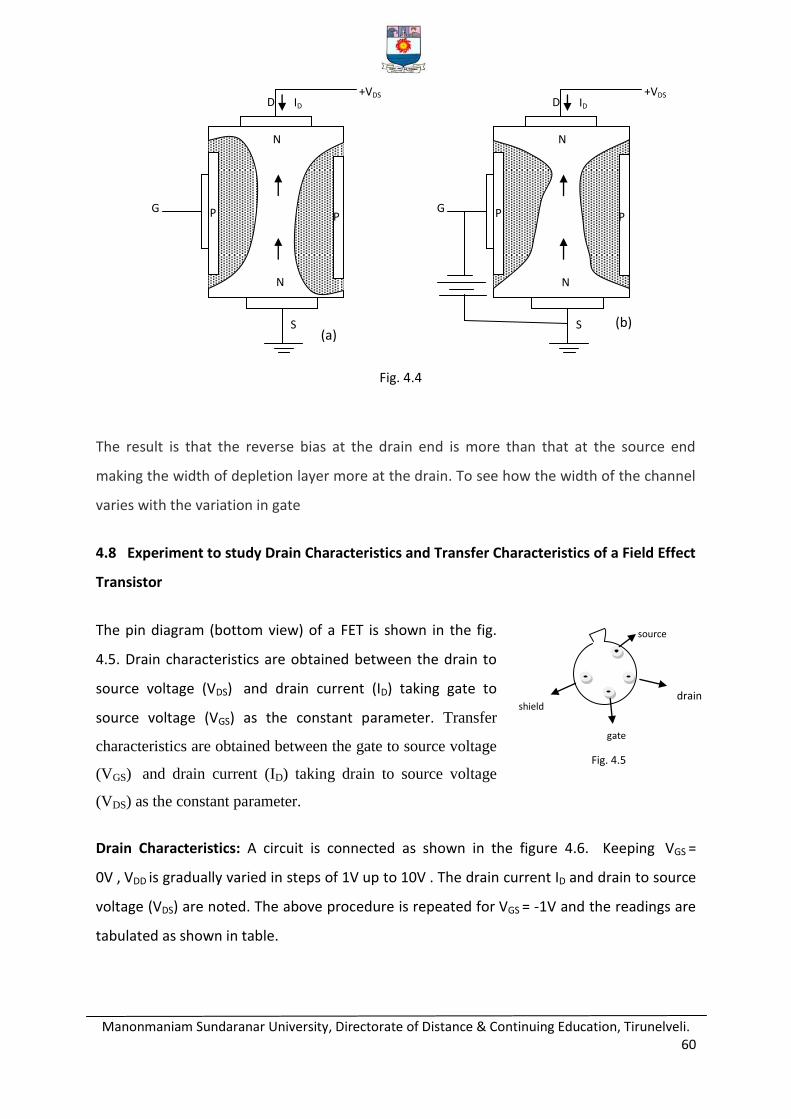
Manonmaniam Sundaranar University, Directorate of Distance & Continuing Education, Tirunelveli. 60
The result is that the reverse bias at the drain end is more than that at the source end
making the width of depletion layer more at the drain. To see how the width of the channel
varies with the variation in gate
4.8 Experiment to study Drain Characteristics and Transfer Characteristics of a Field Effect
Transistor
The pin diagram (bottom view) of a FET is shown in the fig.
4.5. Drain characteristics are obtained between the drain to
source voltage (VDS) and drain current (ID) taking gate to
source voltage (VGS) as the constant parameter. Transfer
characteristics are obtained between the gate to source voltage
(VGS) and drain current (ID) taking drain to source voltage
(VDS) as the constant parameter.
Drain Characteristics: A circuit is connected as shown in the figure 4.6. Keeping VGS =
0V , VDD is gradually varied in steps of 1V up to 10V . The drain current ID and drain to source
voltage (VDS) are noted. The above procedure is repeated for VGS = -1V and the readings are
tabulated as shown in table.
+VDS
G
S
P
N
N
ID D
P P P G
S
P
N
N
ID
+VDS D
P P P
(a) (b)
Fig. 4.4
source
drain shield
gate
Fig. 4.5
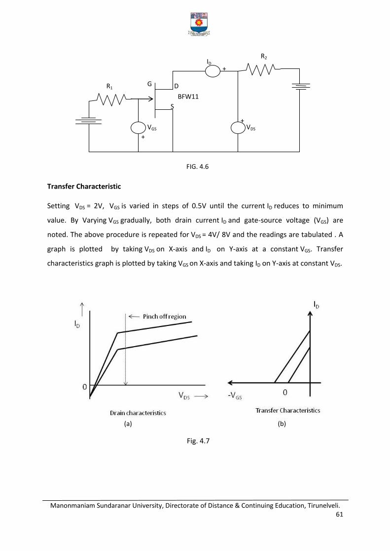
Manonmaniam Sundaranar University, Directorate of Distance & Continuing Education, Tirunelveli. 61
Transfer Characteristic
Setting VDS = 2V, VGS is varied in steps of 0.5V until the current ID reduces to minimum
value. By Varying VGS gradually, both drain current ID and gate-source voltage (VGS) are
noted. The above procedure is repeated for VDS = 4V/ 8V and the readings are tabulated . A
graph is plotted by taking VDS on X-axis and ID on Y-axis at a constant VGS. Transfer
characteristics graph is plotted by taking VGS on X-axis and taking ID on Y-axis at constant VDS.
Fig. 4.7
VDS VGS
ID
G
S
D R1
R2
BFW11
+
+
+
FIG. 4.6
(b) (a)
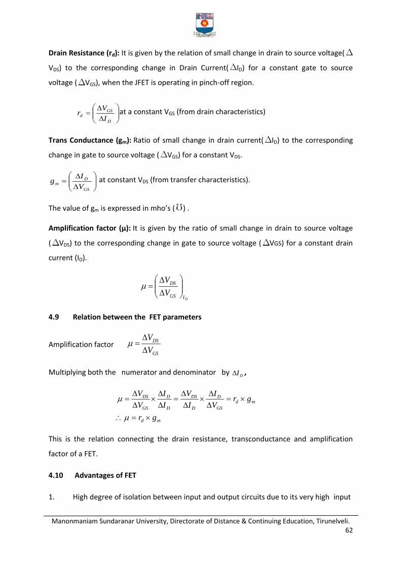
Manonmaniam Sundaranar University, Directorate of Distance & Continuing Education, Tirunelveli. 62
Drain Resistance (rd): It is given by the relation of small change in drain to source voltage(
VDS) to the corresponding change in Drain Current( ID) for a constant gate to source
voltage ( VGS), when the JFET is operating in pinch-off region.
D
GS
dI
Vr at a constant VGS (from drain characteristics)
Trans Conductance (gm): Ratio of small change in drain current( ID) to the corresponding
change in gate to source voltage ( VGS) for a constant VDS.
GS
Dm
V
Ig at constant VDS (from transfer characteristics).
The value of gm is expressed in mho’s ( ) .
Amplification factor (µ): It is given by the ratio of small change in drain to source voltage
( VDS) to the corresponding change in gate to source voltage ( VGS) for a constant drain
current (ID).
DIGS
DS
V
V
4.9 Relation between the FET parameters
Amplification factor GS
DS
V
V
Multiplying both the numerator and denominator by DI ,
md
md
GS
D
D
DS
D
D
GS
DS
gr
grV
I
I
V
I
I
V
V
This is the relation connecting the drain resistance, transconductance and amplification
factor of a FET.
4.10 Advantages of FET
1. High degree of isolation between input and output circuits due to its very high input
Manonmaniam Sundaranar University, Directorate of Distance & Continuing Education, Tirunelveli. 63
impedance
2. Noise is highly reduced due to the absence of junctions
3. It has negative temperature coefficient. So the risk of thermal runaway is avoided.
4. It has high power gain which eliminates the uses of driving stages
5. It has High efficiency and longer life
6. It is relatively immune to radiation.
7. It exhibits no offset voltage at zero drain current and hence makes an excellent
signal chopper.
4.11 Uses of FET
1. FET is suitable for switching analog signals between paths (multiplexing)
due to its large input resistance and low output resistance,
2. it is effective as a buffer in common-drain (source follower) configuration.
3. It is used in switching internal combustion engine ignition coils, where fast switching
and voltage blocking capabilities are important.
4.12 Some Definitions related with FET
Shorted gate drain current (IDSS): It is defined as the drain current when the source is
short circuited to gate (VGS=0) and drain voltage (VDS) equal to pinch off voltage. It is also
called zero bias current.
Pinch off voltage (VP): It is the minimum drain-source voltage at which the drain current
becomes constant.
Gate-source cut off voltage VGS(off): It is the gate-source voltage where the channel is
completely cut off and the drain current becomes zero.
4.13 MOSFET
MOSFET means Metal Oxide Semiconductor Field Effect Transistor. Metal (poly-silicon
doped heavily - metal), Oxide (SiO2 -an insulator), Semiconductor (n-type or p-type), Field
Manonmaniam Sundaranar University, Directorate of Distance & Continuing Education, Tirunelveli. 64
Effect (controlled by an electric field), Transistor (Three terminal device) are used here.
There are two types of MOSFETS namely Depletion type MOSFET (D-MOSFET) and
Enhancement type MOSFET (E-MOSFET). D-type can be operated in both depletion mode
and enhancement mode but E-type can only be operated on enhancement mode only.
The n-channel D-MOSFET is a piece of n-type material with a p-type region called substrate
on the right side and an insulated gate on the left as shown. The free electrons flowing from
source to drain must pass through the narrow channel between the gate and the p-type
region .
The Gate construction of D-MOSFET is explained as follows
A thin layer of metal oxide, usually silicon dioxide (SiO2) is deposited over a small portion of
the channel. A metallic gate is deposited over the oxide layer. As SiO2 is an insulator,
therefore, gate is insulated from the channel. The substrate is connected to the source
internally so that a MOSFET has three terminals such as Source (S), Gate (G) and Drain(D).
Since the gate is insulated from the channel, we can apply either negative or positive
voltage to the gate. Therefore, D-MOSFET can be operated in both depletion-mode and
enhancement-mode.
Again, there are two types of D-MOSFETs namely, n-channel D-MOSFET, p-channel D-
MOSFET
n-channel D-MOSFET
Figure 4.8 shows the various parts of n-channel D-MOSFET. The p-type substrate constricts
the channel between the source and drain so that only a small passage remains at the left
side. Electrons flowing from source (when drain is positive w.r.t. source) must pass through
this narrow channel. The symbol used for n-channel D-MOSFET is shown in fig. 4.9(a). The
gate appears like a capacitor plate. Just to the right of the gate is a thick vertical line
representing the channel. The drain lead comes out of the top of the channel and the source
lead connects to the bottom. The arrow is on the substrate and points to the n-material,
therefore we have n-channel D-MOSFET. The substrate is connected to the source as shown
in fig. 4.9(b). This gives rise to a three terminal device.
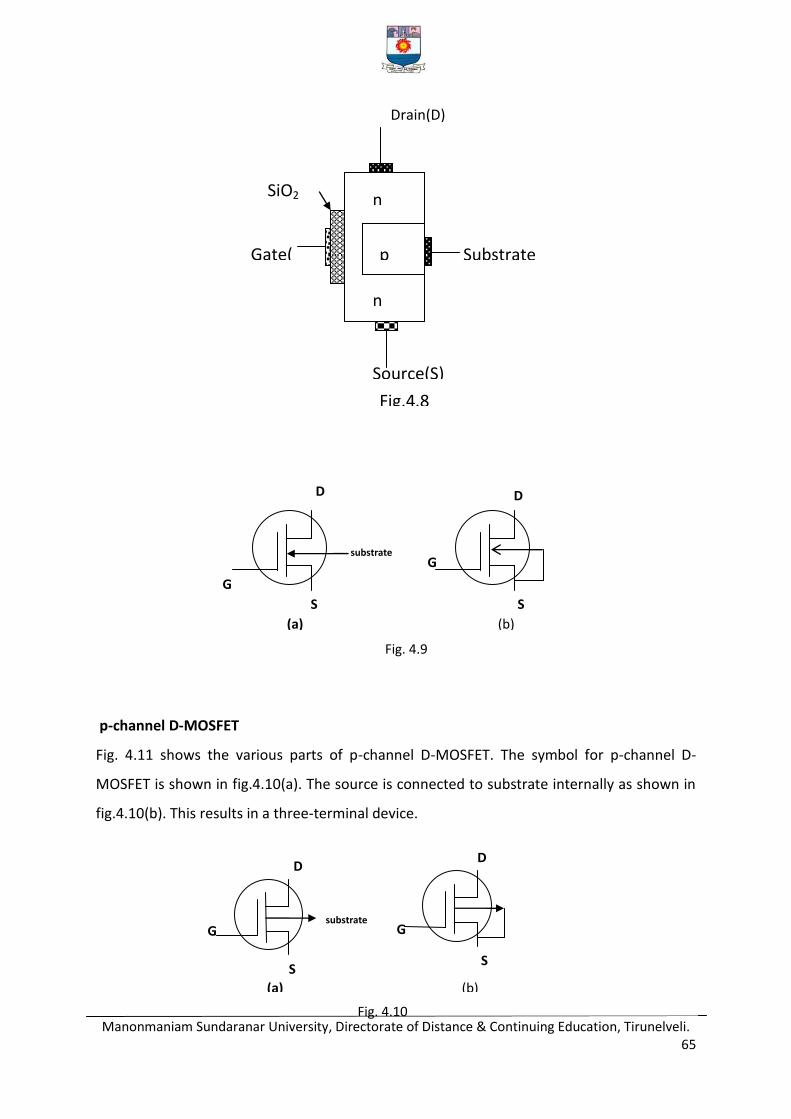
Manonmaniam Sundaranar University, Directorate of Distance & Continuing Education, Tirunelveli. 65
p-channel D-MOSFET
Fig. 4.11 shows the various parts of p-channel D-MOSFET. The symbol for p-channel D-
MOSFET is shown in fig.4.10(a). The source is connected to substrate internally as shown in
fig.4.10(b). This results in a three-terminal device.
S
D
G
S
D
G substrate
(a) (b)
Fig. 4.9
G
D D
S S
G substrate
(a) (b)
Fig. 4.10
n
n
p
Drain(D)
Source(S)
Substrate Gate(
G)
SiO2
Layer
Fig.4.8
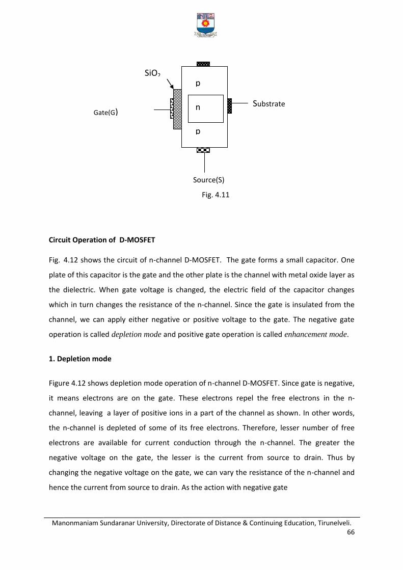
Manonmaniam Sundaranar University, Directorate of Distance & Continuing Education, Tirunelveli. 66
Circuit Operation of D-MOSFET
Fig. 4.12 shows the circuit of n-channel D-MOSFET. The gate forms a small capacitor. One
plate of this capacitor is the gate and the other plate is the channel with metal oxide layer as
the dielectric. When gate voltage is changed, the electric field of the capacitor changes
which in turn changes the resistance of the n-channel. Since the gate is insulated from the
channel, we can apply either negative or positive voltage to the gate. The negative gate
operation is called depletion mode and positive gate operation is called enhancement mode.
1. Depletion mode
Figure 4.12 shows depletion mode operation of n-channel D-MOSFET. Since gate is negative,
it means electrons are on the gate. These electrons repel the free electrons in the n-
channel, leaving a layer of positive ions in a part of the channel as shown. In other words,
the n-channel is depleted of some of its free electrons. Therefore, lesser number of free
electrons are available for current conduction through the n-channel. The greater the
negative voltage on the gate, the lesser is the current from source to drain. Thus by
changing the negative voltage on the gate, we can vary the resistance of the n-channel and
hence the current from source to drain. As the action with negative gate
Gate(G)
SiO2
Layer
Substrate
Source(S)
Fig. 4.11
p
n
p
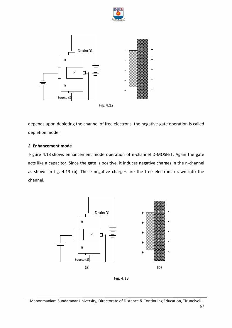
Manonmaniam Sundaranar University, Directorate of Distance & Continuing Education, Tirunelveli. 67
depends upon depleting the channel of free electrons, the negative-gate operation is called
depletion mode.
2. Enhancement mode
Figure 4.13 shows enhancement mode operation of n-channel D-MOSFET. Again the gate
acts like a capacitor. Since the gate is positive, it induces negative charges in the n-channel
as shown in fig. 4.13 (b). These negative charges are the free electrons drawn into the
channel.
n
n
p
Drain(D)
Source (S)
-
-
-
-
-
+
+
+
+
+
Fig. 4.12
n
n
p
Drain(D)
Source (S)
+
+
+
+
+
-
-
-
-
-
Fig. 4.13
(a) (b)
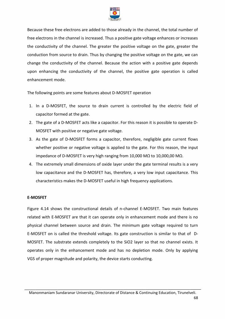
Manonmaniam Sundaranar University, Directorate of Distance & Continuing Education, Tirunelveli. 68
Because these free electrons are added to those already in the channel, the total number of
free electrons in the channel is increased. Thus a positive gate voltage enhances or increases
the conductivity of the channel. The greater the positive voltage on the gate, greater the
conduction from source to drain. Thus by changing the positive voltage on the gate, we can
change the conductivity of the channel. Because the action with a positive gate depends
upon enhancing the conductivity of the channel, the positive gate operation is called
enhancement mode.
The following points are some features about D-MOSFET operation
1. In a D-MOSFET, the source to drain current is controlled by the electric field of
capacitor formed at the gate.
2. The gate of a D-MOSFET acts like a capacitor. For this reason it is possible to operate D-
MOSFET with positive or negative gate voltage.
3. As the gate of D-MOSFET forms a capacitor, therefore, negligible gate current flows
whether positive or negative voltage is applied to the gate. For this reason, the input
impedance of D-MOSFET is very high ranging from 10,000 MΩ to 10,000,00 MΩ.
4. The extremely small dimensions of oxide layer under the gate terminal results is a very
low capacitance and the D-MOSFET has, therefore, a very low input capacitance. This
characteristics makes the D-MOSFET useful in high frequency applications.
E-MOSFET
Figure 4.14 shows the constructional details of n-channel E-MOSFET. Two main features
related with E-MOSFET are that it can operate only in enhancement mode and there is no
physical channel between source and drain. The minimum gate voltage required to turn
E-MOSFET on is called the threshold voltage. Its gate construction is similar to that of D-
MOSFET. The substrate extends completely to the SiO2 layer so that no channel exists. It
operates only in the enhancement mode and has no depletion mode. Only by applying
VGS of proper magnitude and polarity, the device starts conducting.
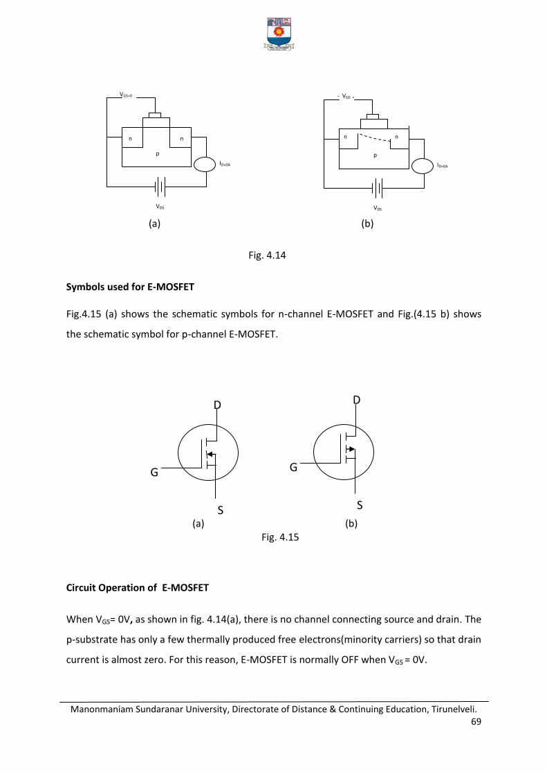
Manonmaniam Sundaranar University, Directorate of Distance & Continuing Education, Tirunelveli. 69
(a) (b)
Fig. 4.14
Symbols used for E-MOSFET
Fig.4.15 (a) shows the schematic symbols for n-channel E-MOSFET and Fig.(4.15 b) shows
the schematic symbol for p-channel E-MOSFET.
Circuit Operation of E-MOSFET
When VGS= 0V, as shown in fig. 4.14(a), there is no channel connecting source and drain. The
p-substrate has only a few thermally produced free electrons(minority carriers) so that drain
current is almost zero. For this reason, E-MOSFET is normally OFF when VGS = 0V.
VGS=0
n n
p
ID=0A
VDS
- VGS +
p
ID>0A
VDS
n n
D
S
G
D
S
G
(a) (b) Fig. 4.15
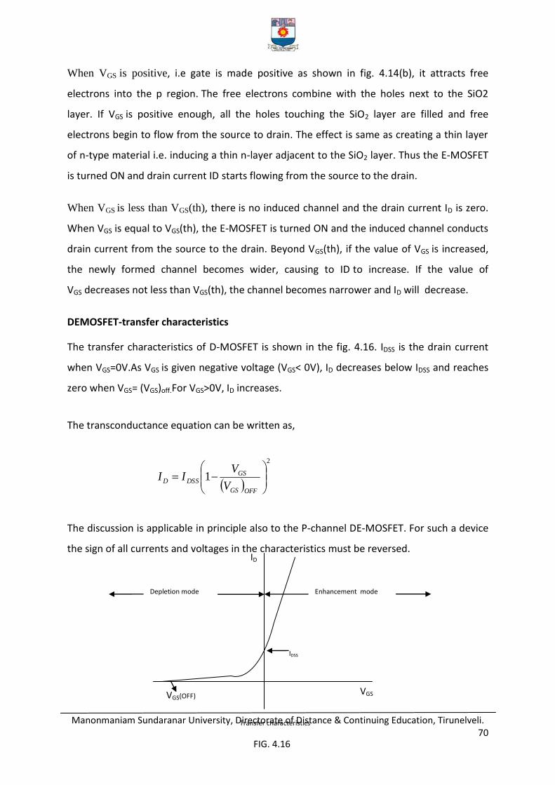
Manonmaniam Sundaranar University, Directorate of Distance & Continuing Education, Tirunelveli. 70
When VGS is positive, i.e gate is made positive as shown in fig. 4.14(b), it attracts free
electrons into the p region. The free electrons combine with the holes next to the SiO2
layer. If VGS is positive enough, all the holes touching the SiO2 layer are filled and free
electrons begin to flow from the source to drain. The effect is same as creating a thin layer
of n-type material i.e. inducing a thin n-layer adjacent to the SiO2 layer. Thus the E-MOSFET
is turned ON and drain current ID starts flowing from the source to the drain.
When VGS is less than VGS(th), there is no induced channel and the drain current ID is zero.
When VGS is equal to VGS(th), the E-MOSFET is turned ON and the induced channel conducts
drain current from the source to the drain. Beyond VGS(th), if the value of VGS is increased,
the newly formed channel becomes wider, causing to ID to increase. If the value of
VGS decreases not less than VGS(th), the channel becomes narrower and ID will decrease.
DEMOSFET-transfer characteristics
The transfer characteristics of D-MOSFET is shown in the fig. 4.16. IDSS is the drain current
when VGS=0V.As VGS is given negative voltage (VGS< 0V), ID decreases below IDSS and reaches
zero when VGS= (VGS)off.For VGS>0V, ID increases.
The transconductance equation can be written as,
2
1
OFFGS
GSDSSD
V
VII
The discussion is applicable in principle also to the P-channel DE-MOSFET. For such a device
the sign of all currents and voltages in the characteristics must be reversed.
ID
VGS
Depletion mode Enhancement mode
IDSS
Transfer characteristics
VGS(OFF)
FIG. 4.16
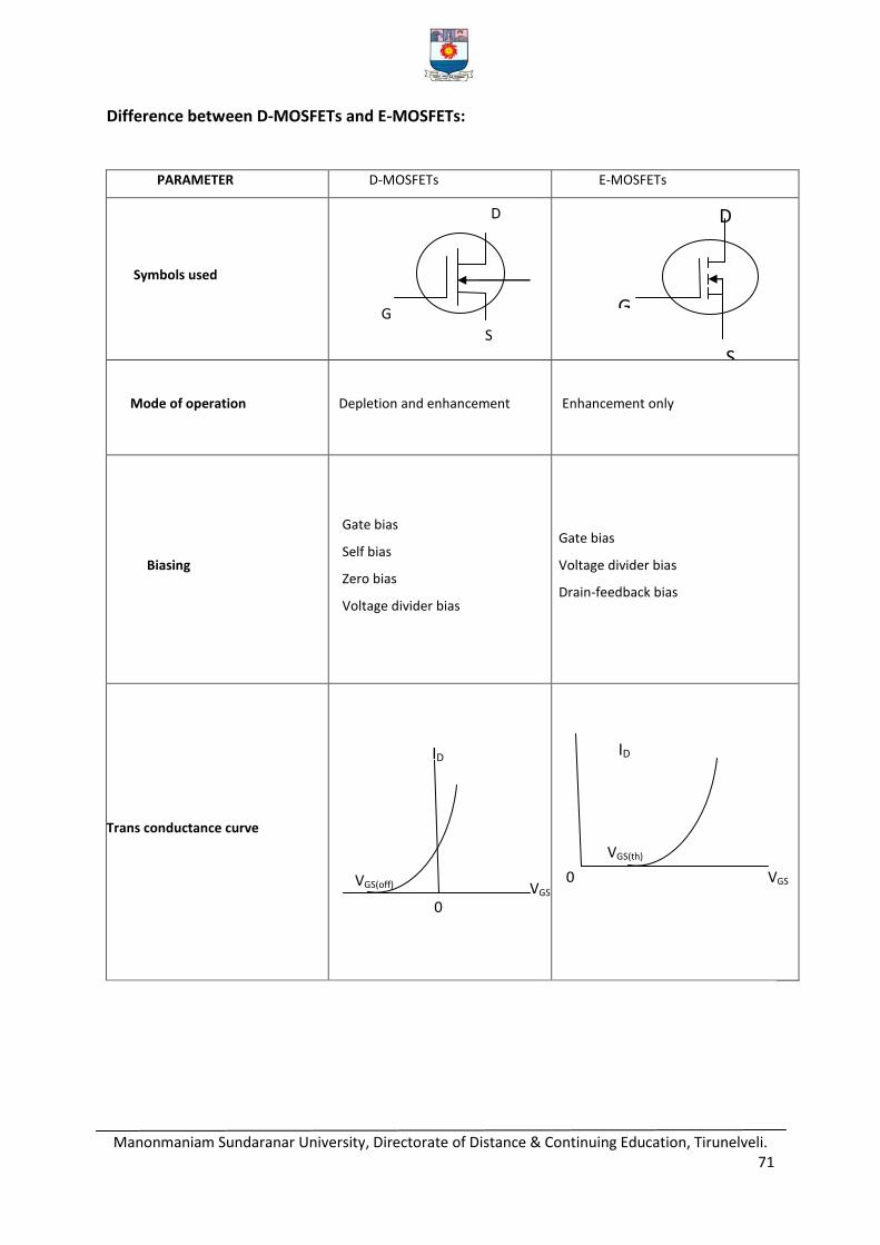
Manonmaniam Sundaranar University, Directorate of Distance & Continuing Education, Tirunelveli. 71
Difference between D-MOSFETs and E-MOSFETs:
PARAMETER D-MOSFETs E-MOSFETs
Symbols used
Mode of operation
Depletion and enhancement Enhancement only
Biasing
Gate bias
Self bias
Zero bias
Voltage divider bias
Gate bias
Voltage divider bias
Drain-feedback bias
Trans conductance curve
ID ID
VGS VGS
0
0
VGS(off)
VGS(th)
S
D
G
D
S
G
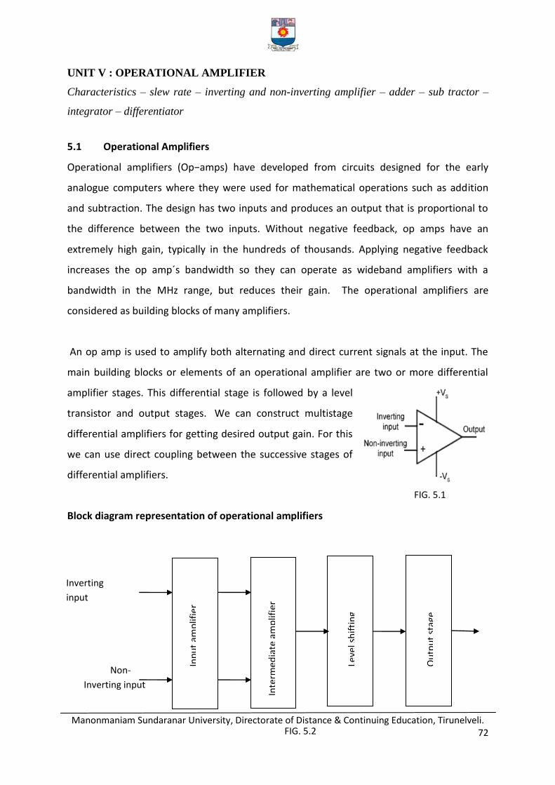
Manonmaniam Sundaranar University, Directorate of Distance & Continuing Education, Tirunelveli. 72
UNIT V : OPERATIONAL AMPLIFIER
Characteristics – slew rate – inverting and non-inverting amplifier – adder – sub tractor –
integrator – differentiator
5.1 Operational Amplifiers
Operational amplifiers (Op−amps) have developed from circuits designed for the early
analogue computers where they were used for mathematical operations such as addition
and subtraction. The design has two inputs and produces an output that is proportional to
the difference between the two inputs. Without negative feedback, op amps have an
extremely high gain, typically in the hundreds of thousands. Applying negative feedback
increases the op amp´s bandwidth so they can operate as wideband amplifiers with a
bandwidth in the MHz range, but reduces their gain. The operational amplifiers are
considered as building blocks of many amplifiers.
An op amp is used to amplify both alternating and direct current signals at the input. The
main building blocks or elements of an operational amplifier are two or more differential
amplifier stages. This differential stage is followed by a level
transistor and output stages. We can construct multistage
differential amplifiers for getting desired output gain. For this
we can use direct coupling between the successive stages of
differential amplifiers.
Block diagram representation of operational amplifiers
Inp
ut
amp
lifie
r
Inte
rmed
iate
am
plif
ier
Leve
l sh
ifti
ng
Ou
tpu
t st
age
Non-
Inverting input
Inverting
input
FIG. 5.2
FIG. 5.1
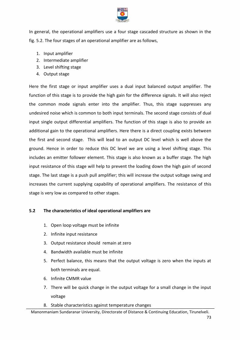
Manonmaniam Sundaranar University, Directorate of Distance & Continuing Education, Tirunelveli. 73
In general, the operational amplifiers use a four stage cascaded structure as shown in the
fig. 5.2. The four stages of an operational amplifier are as follows,
1. Input amplifier
2. Intermediate amplifier
3. Level shifting stage
4. Output stage
Here the first stage or input amplifier uses a dual input balanced output amplifier. The
function of this stage is to provide the high gain for the difference signals. It will also reject
the common mode signals enter into the amplifier. Thus, this stage suppresses any
undesired noise which is common to both input terminals. The second stage consists of dual
input single output differential amplifiers. The function of this stage is also to provide an
additional gain to the operational amplifiers. Here there is a direct coupling exists between
the first and second stage. This will lead to an output DC level which is well above the
ground. Hence in order to reduce this DC level we are using a level shifting stage. This
includes an emitter follower element. This stage is also known as a buffer stage. The high
input resistance of this stage will help to prevent the loading down the high gain of second
stage. The last stage is a push pull amplifier; this will increase the output voltage swing and
increases the current supplying capability of operational amplifiers. The resistance of this
stage is very low as compared to other stages.
5.2 The characteristics of ideal operational amplifiers are
1. Open loop voltage must be infinite
2. Infinite input resistance
3. Output resistance should remain at zero
4. Bandwidth available must be infinite
5. Perfect balance, this means that the output voltage is zero when the inputs at
both terminals are equal.
6. Infinite CMMR value
7. There will be quick change in the output voltage for a small change in the input
voltage
8. Stable characteristics against temperature changes
Manonmaniam Sundaranar University, Directorate of Distance & Continuing Education, Tirunelveli. 74
(i) Open loop gain
The main function of an operational amplifier is to amplify the input signal and the
more open loop gain it has the better. Open-loop gain is the gain of the op-amp
without positive or negative feedback and for such an amplifier the gain will be
infinite but typical real values range from about 20,000 to 200,000.
(ii) Input impedance (Zin)
Input impedance is the ratio of input voltage to input current and is assumed to be
infinite to prevent any current flowing from the source supply into the amplifiers input
circuitry ( Iin = 0 ). Real op-amps have input leakage currents from a few pico-amps to a
few milli-amps.
(iii) Output impedance (Zout)
The output impedance of the ideal operational amplifier is assumed to be zero acting
as a perfect internal voltage source with no internal resistance so that it can supply as
much current as necessary to the load. This internal resistance is effectively in series
with the load thereby reducing the output voltage available to the load. Real op-amps
have output impedances in the 100-20kΩ range.
(iv) Bandwidth (GBW)
An ideal operational amplifier has an infinite frequency response and can amplify any
frequency signal from DC to the highest AC frequencies so it is therefore assumed to
have an infinite bandwidth. With real op-amps, the bandwidth is limited by the Gain-
Bandwidth product (GBW), which is equal to the frequency where the amplifiers gain
becomes unity.
(v) Input Offset Voltage (Vio)
The input offset voltage is a parameter defining the differential DC voltage required
between the inputs of an amplifier to make the output zero
Manonmaniam Sundaranar University, Directorate of Distance & Continuing Education, Tirunelveli. 75
5.3 Reason for high popularity of operational amplifiers
1) Its characteristics are near to the ideal one
2) It is very easy to design
3) They work at different levels quite close to the theoretical performance
4) It provides high reliability
5) It can be available in small packages
6) Reduced cost and stable performance against temperature variations
5.4 Operational Amplifier Basics
An op-amp is fundamentally a voltage amplifying device designed to be used with external
feedback components such as resistors and capacitors between its output and input
terminals. These feedback components determine the resulting function or operation of the
amplifier and by virtue of the different feedback configurations whether resistive, capacitive
or both, the amplifier can perform a variety of different operations, giving rise to its name of
Operational Amplifier.
An Operational Amplifier is basically a three-terminal device which consists of two high
impedance inputs, one called the Inverting Input, marked with a negative sign, ( – ) and the
other one called the non-inverting Input, marked with a positive or ( + ).
5.5 Differential amplifiers
A differential amplifier is a circuit made up of transistors which is used to amplify the
difference between the input signals. Here in differential amplifiers, when same input is
given to both input terminals then the output voltage will be zero. A small difference in the
input voltages may lead to large gain at the output. These types of differential amplifiers has
many advantages.
The circuit in fig. 5.3 shows a
generalized form of a differential
amplifier with two inputs. The two
identical transistors T1 and T2 are
RE
RC1
FIG. 5.3
INPUT 2
OUTPUT RC2
-VEE
T2 T1
+VCC
INPUT 1
Manonmaniam Sundaranar University, Directorate of Distance & Continuing Education, Tirunelveli. 76
both biased at the same operating point with their emitters connected together and
returned to the common rail, -VEE by way of resistor RE. The circuit operates from a dual
supply +Vcc and -VEE which ensures a constant supply. The voltage that appears at the
output (Vout ) of the amplifier is the difference between the two input signals as the two
base inputs are in anti-phase with each other. So as the forward bias of transistor T1 is
increased, the forward bias of transistor T2 is reduced and vice versa. Then if the two
transistors are perfectly matched, the current flowing through the common emitter resistor,
RE will remain constant.
Operational Amplifiers also have one output of low impedance that is referenced to a
common ground terminal and it should ignore any common mode signals, that is, if an
identical signal is applied to both the inverting and non-inverting inputs there should no
change to the output.
Operational Amplifiers on their own have a very high open loop DC gain and by applying
some form of negative feedback, We can produce an operational amplifier circuit that has a
very precise gain characteristic that is dependent only on the feedback used.
An op amp only responds to the difference between the voltages on its two input terminals,
known commonly as the Differential Input Voltage and not to their common potential. Then
if the same voltage potential is applied to both terminals the resultant output will be zero.
An Operational Amplifiers gain is commonly known as the Open Loop Differential Gain, and
is given the symbol (A0).
5.3 Common Mode Rejection Ratio (CMRR)
CMMR of a differential amplifier measures the ability of the device to reject common-mode
signals, that appear simultaneously and in-phase on both amplifier inputs. An ideal
differential amplifier would have infinite CMRR; this is not achievable in practice. A high
CMRR is required when a differential signal must be amplified in the presence of a possibly
large common-mode input. An example is audio transmission over balanced lines. The
CMRR is defined as the ratio of the powers of the differential gain over the common-mode
gain, measured in positive decibels (using the 20 log rule):
Manonmaniam Sundaranar University, Directorate of Distance & Continuing Education, Tirunelveli. 77
dBA
A
A
ACMRR
cm
d
cm
d
2
10log10
(5.1)
As differential gain should exceed common-mode gain, this will be a positive number, and
the higher the better. The CMRR is a very important specification, as it indicates how much
of the common-mode signal will appear in the measurement. The value of the CMRR often
depends on signal frequency.
It is often important in reducing noise on transmission lines. For example, when measuring
the resistance of a thermocouple in a noisy environment, the noise from the environment
appears as an offset on both input leads, making it a common-mode voltage signal. The
CMRR of the measurement instrument determines the attenuation applied to the offset or
noise.
Problem: A differential amplifier has a differential voltage gain of 1V with a
differential input of 2.5mV and an output of 2 mV with a common mode input of 5 mV.
Find the CMRR in dB.
Differential gain ADM=1V/2.5MV=400
Common mode gain ACM=2MV/5MV=0.4
CMRRdb=20log(400/0.4)=20log1000=40dB
5.4 Bandwidth of an op amp
Every op amp has its own bandwidth. It depends upon the closed loop gain of the op amp.
Gain Band width product (GBW) is defined as
unityCL ffAGBW where CLA = closed loop gain at the frequency f and unityf is the
frequency at which the closed loop gain is unity. The gain-bandwidth product is always
constant
An op amp has GBW of 100MHz. Find the band width of the op amp when the closed loop
gain value is 100. Find the maximum value of the closed loop gain at 200 KHz.
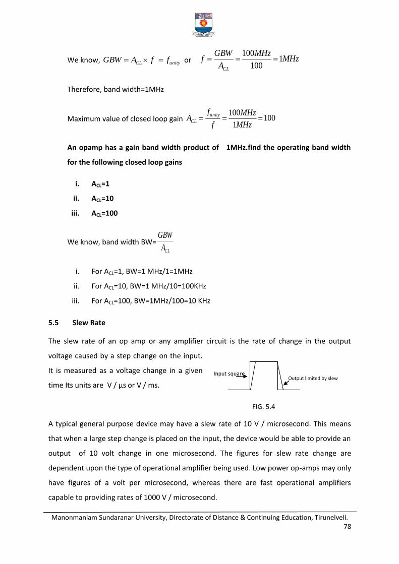
Manonmaniam Sundaranar University, Directorate of Distance & Continuing Education, Tirunelveli. 78
We know, unityCL ffAGBW or MHzMHz
A
GBWf
CL
1100
100
Therefore, band width=1MHz
Maximum value of closed loop gain 1001
100
MHz
MHz
f
fA
unity
CL
An opamp has a gain band width product of 1MHz.find the operating band width
for the following closed loop gains
i. ACL=1
ii. ACL=10
iii. ACL=100
We know, band width BW=CLA
GBW
i. For ACL=1, BW=1 MHz/1=1MHz
ii. For ACL=10, BW=1 MHz/10=100KHz
iii. For ACL=100, BW=1MHz/100=10 KHz
5.5 Slew Rate
The slew rate of an op amp or any amplifier circuit is the rate of change in the output
voltage caused by a step change on the input.
It is measured as a voltage change in a given
time Its units are V / µs or V / ms.
A typical general purpose device may have a slew rate of 10 V / microsecond. This means
that when a large step change is placed on the input, the device would be able to provide an
output of 10 volt change in one microsecond. The figures for slew rate change are
dependent upon the type of operational amplifier being used. Low power op-amps may only
have figures of a volt per microsecond, whereas there are fast operational amplifiers
capable to providing rates of 1000 V / microsecond.
Input square
wave Output limited by slew
rate
FIG. 5.4
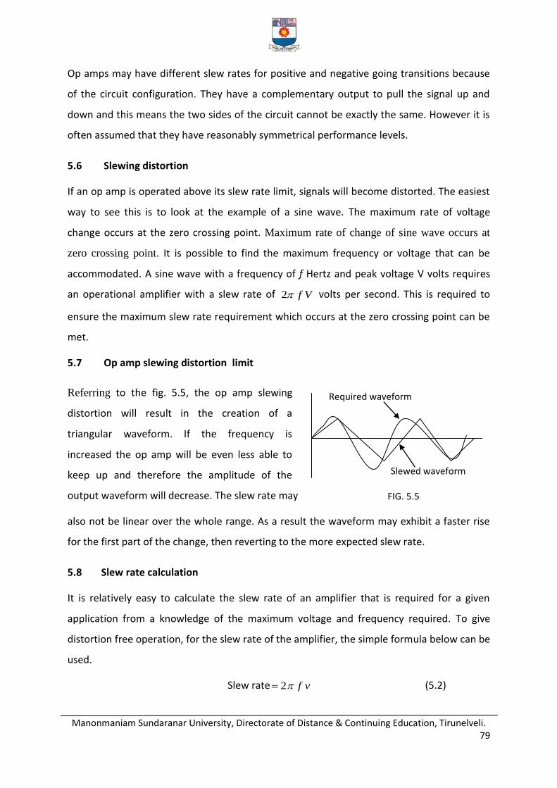
Manonmaniam Sundaranar University, Directorate of Distance & Continuing Education, Tirunelveli. 79
Op amps may have different slew rates for positive and negative going transitions because
of the circuit configuration. They have a complementary output to pull the signal up and
down and this means the two sides of the circuit cannot be exactly the same. However it is
often assumed that they have reasonably symmetrical performance levels.
5.6 Slewing distortion
If an op amp is operated above its slew rate limit, signals will become distorted. The easiest
way to see this is to look at the example of a sine wave. The maximum rate of voltage
change occurs at the zero crossing point. Maximum rate of change of sine wave occurs at
zero crossing point. It is possible to find the maximum frequency or voltage that can be
accommodated. A sine wave with a frequency of f Hertz and peak voltage V volts requires
an operational amplifier with a slew rate of Vf2 volts per second. This is required to
ensure the maximum slew rate requirement which occurs at the zero crossing point can be
met.
5.7 Op amp slewing distortion limit
Referring to the fig. 5.5, the op amp slewing
distortion will result in the creation of a
triangular waveform. If the frequency is
increased the op amp will be even less able to
keep up and therefore the amplitude of the
output waveform will decrease. The slew rate may
also not be linear over the whole range. As a result the waveform may exhibit a faster rise
for the first part of the change, then reverting to the more expected slew rate.
5.8 Slew rate calculation
It is relatively easy to calculate the slew rate of an amplifier that is required for a given
application from a knowledge of the maximum voltage and frequency required. To give
distortion free operation, for the slew rate of the amplifier, the simple formula below can be
used.
Slew rate vf2 (5.2)
Slewed waveform
Required waveform
FIG. 5.5
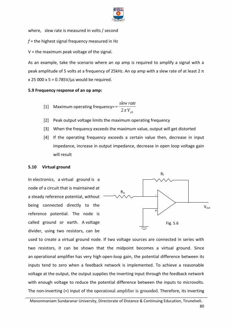
Manonmaniam Sundaranar University, Directorate of Distance & Continuing Education, Tirunelveli. 80
where, slew rate is measured in volts / second
f = the highest signal frequency measured in Hz
V = the maximum peak voltage of the signal.
As an example, take the scenario where an op amp is required to amplify a signal with a
peak amplitude of 5 volts at a frequency of 25kHz. An op amp with a slew rate of at least 2 π
x 25 000 x 5 = 0.785V/µs would be required.
5.9 Frequency response of an op amp:
[1] Maximum operating frequency=pkV
rateslew
2
[2] Peak output voltage limits the maximum operating frequency
[3] When the frequency exceeds the maximum value, output will get distorted
[4] If the operating frequency exceeds a certain value then, decrease in input
impedance, increase in output impedance, decrease in open loop voltage gain
will result
5.10 Virtual ground
In electronics, a virtual ground is a
node of a circuit that is maintained at
a steady reference potential, without
being connected directly to the
reference potential. The node is
called ground or earth. A voltage
divider, using two resistors, can be
used to create a virtual ground node. If two voltage sources are connected in series with
two resistors, it can be shown that the midpoint becomes a virtual ground. Since
an operational amplifier has very high open-loop gain, the potential difference between its
inputs tend to zero when a feedback network is implemented. To achieve a reasonable
voltage at the output, the output supplies the inverting input through the feedback network
with enough voltage to reduce the potential difference between the inputs to microvolts.
The non-inverting (+) input of the operational amplifier is grounded. Therefore, its inverting
Rin
Rf
Vout +
-
Fig. 5.6
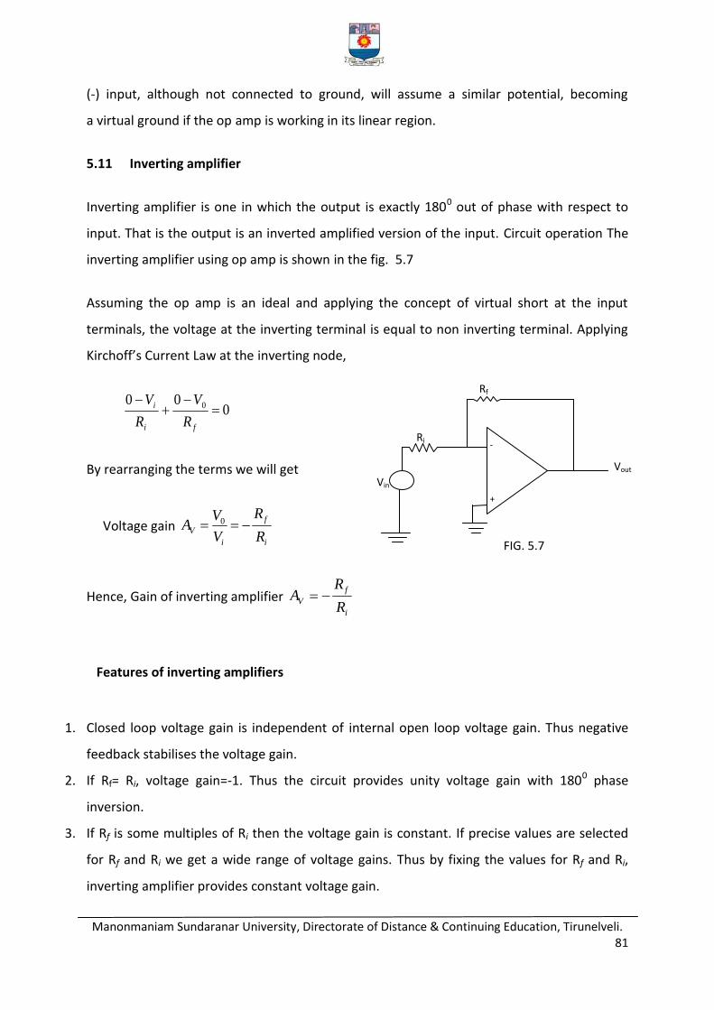
Manonmaniam Sundaranar University, Directorate of Distance & Continuing Education, Tirunelveli. 81
(-) input, although not connected to ground, will assume a similar potential, becoming
a virtual ground if the op amp is working in its linear region.
5.11 Inverting amplifier
Inverting amplifier is one in which the output is exactly 1800 out of phase with respect to
input. That is the output is an inverted amplified version of the input. Circuit operation The
inverting amplifier using op amp is shown in the fig. 5.7
Assuming the op amp is an ideal and applying the concept of virtual short at the input
terminals, the voltage at the inverting terminal is equal to non inverting terminal. Applying
Kirchoff’s Current Law at the inverting node,
000 0
fi
i
R
V
R
V
By rearranging the terms we will get
Voltage gain i
f
i
VR
R
V
VA 0
Hence, Gain of inverting amplifier i
f
VR
RA
Features of inverting amplifiers
1. Closed loop voltage gain is independent of internal open loop voltage gain. Thus negative
feedback stabilises the voltage gain.
2. If Rf= Ri, voltage gain=-1. Thus the circuit provides unity voltage gain with 1800 phase
inversion.
3. If Rf is some multiples of Ri then the voltage gain is constant. If precise values are selected
for Rf and Ri we get a wide range of voltage gains. Thus by fixing the values for Rf and Ri,
inverting amplifier provides constant voltage gain.
Rf
Ri
Vin
Vout
+
-
FIG. 5.7
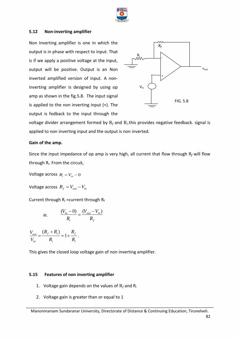
Manonmaniam Sundaranar University, Directorate of Distance & Continuing Education, Tirunelveli. 82
5.12 Non-inverting amplifier
Non Inverting amplifier is one in which the
output is in phase with respect to input. That
is if we apply a positive voltage at the input,
output will be positive. Output is an Non
inverted amplified version of input. A non-
inverting amplifier is designed by using op
amp as shown in the fig.5.8. The input signal
is applied to the non inverting input (+). The
output is fedback to the input through the
voltage divider arrangement formed by Rf and Ri.this provides negative feedback. signal is
applied to non inverting input and the output is non inverted.
Gain of the amp.
Since the input impedance of op amp is very high, all current that flow through Rf will flow
through Ri. From the circuit,
Voltage across 0 ini VR
Voltage across inoutf VVR
Current through Ri =current through Rf
ie. f
inout
i
in
R
VV
R
V )()0(
i
f
i
if
in
out
R
R
R
RR
V
V
1
)(.
This gives the closed loop voltage gain of non inverting amplifier.
5.15 Features of non inverting amplifier
1. Voltage gain depends on the values of Rf and Ri
2. Voltage gain is greater than or equal to 1
Ri
Vin
Vout
+
-
FIG. 5.8
Rf
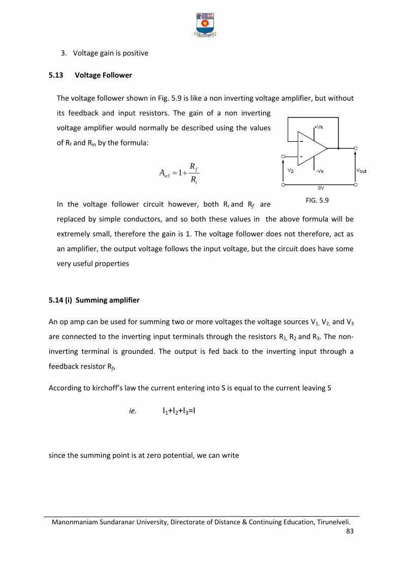
Manonmaniam Sundaranar University, Directorate of Distance & Continuing Education, Tirunelveli. 83
3. Voltage gain is positive
5.13 Voltage Follower
The voltage follower shown in Fig. 5.9 is like a non inverting voltage amplifier, but without
its feedback and input resistors. The gain of a non inverting
voltage amplifier would normally be described using the values
of Rf and Rin by the formula:
i
f
vclR
RA 1
In the voltage follower circuit however, both Ri and Rf are
replaced by simple conductors, and so both these values in the above formula will be
extremely small, therefore the gain is 1. The voltage follower does not therefore, act as
an amplifier, the output voltage follows the input voltage, but the circuit does have some
very useful properties
5.14 (i) Summing amplifier
An op amp can be used for summing two or more voltages the voltage sources V1, V2, and V3
are connected to the inverting input terminals through the resistors R1, R2 and R3. The non-
inverting terminal is grounded. The output is fed back to the inverting input through a
feedback resistor Rf,
According to kirchoff’s law the current entering into S is equal to the current leaving S
ie. I1+I2+I3=I
since the summing point is at zero potential, we can write
FIG. 5.9
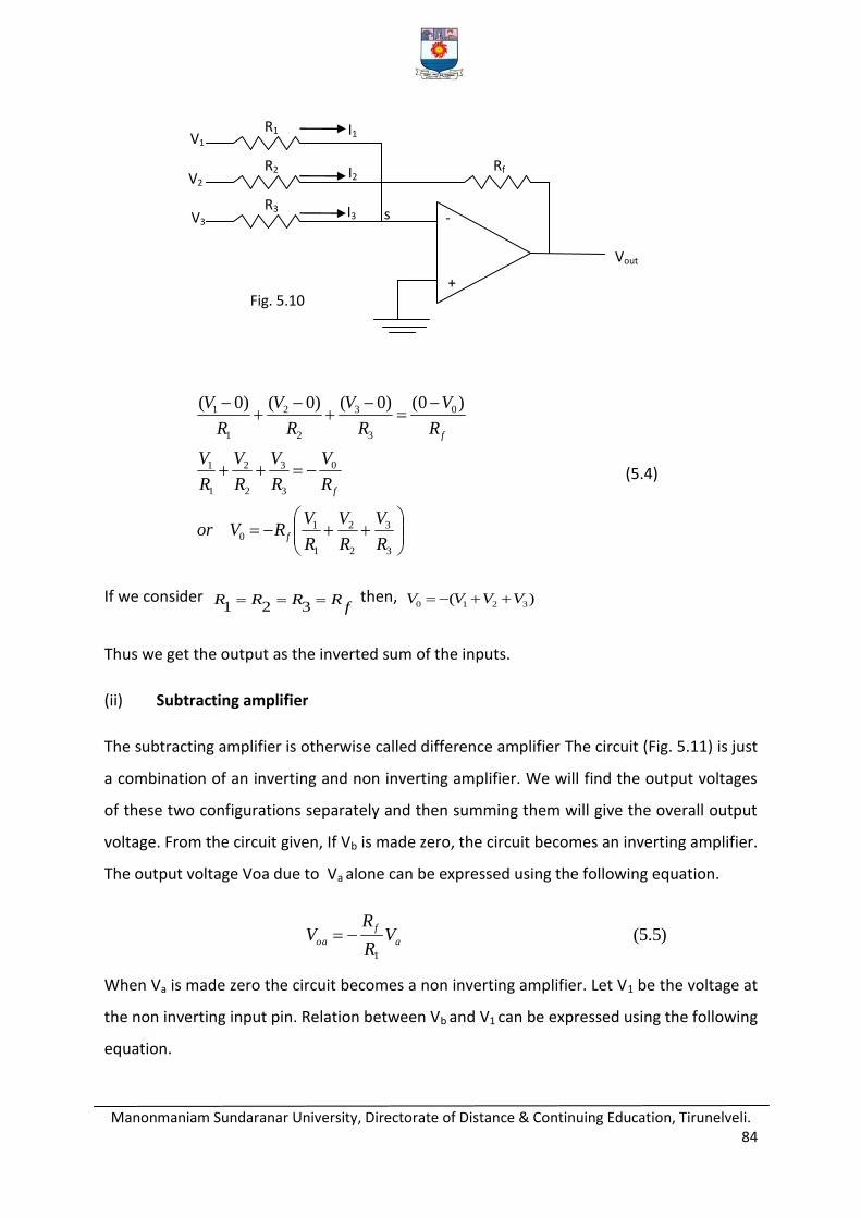
Manonmaniam Sundaranar University, Directorate of Distance & Continuing Education, Tirunelveli. 84
3
3
2
2
1
10
0
3
3
2
2
1
1
0
3
3
2
2
1
1 )0()0()0()0(
R
V
R
V
R
VRVor
R
V
R
V
R
V
R
V
R
V
R
V
R
V
R
V
f
f
f
(5.4)
If we consider f
RRRR 321
then, )( 3210 VVVV
Thus we get the output as the inverted sum of the inputs.
(ii) Subtracting amplifier
The subtracting amplifier is otherwise called difference amplifier The circuit (Fig. 5.11) is just
a combination of an inverting and non inverting amplifier. We will find the output voltages
of these two configurations separately and then summing them will give the overall output
voltage. From the circuit given, If Vb is made zero, the circuit becomes an inverting amplifier.
The output voltage Voa due to Va alone can be expressed using the following equation.
)5.5(1
a
f
oa VR
RV
When Va is made zero the circuit becomes a non inverting amplifier. Let V1 be the voltage at
the non inverting input pin. Relation between Vb and V1 can be expressed using the following
equation.
Vout
Rf
R1
R2
R3
V1
V2
V3 -
+
Fig. 5.10
I1
I2
I3 s
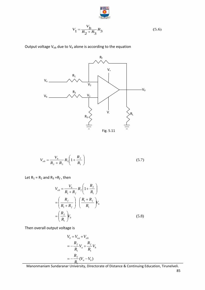
Manonmaniam Sundaranar University, Directorate of Distance & Continuing Education, Tirunelveli. 85
)6.5(
332
1R
RRb
VV
Output voltage Vob due to Vb alone is according to the equation
)7.5(11
3
32
R
RR
RR
VV
fb
ob
Let R1 = R2 and R3 =Rf , then
)8.5(
1
1
1
1
1
11
b
f
b
f
f
f
f
f
f
bob
VR
R
VR
RR
RR
R
R
RR
RR
VV
Then overall output voltage is
)(1
11
0
ba
f
b
f
a
f
oboa
VVR
R
VR
RV
R
R
VVV
Va
Vb
R1
R2
Rf
V1
V2
V+
V- RL R3
V0
Fig. 5.11
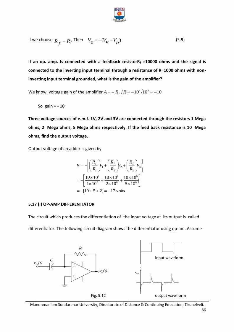
Manonmaniam Sundaranar University, Directorate of Distance & Continuing Education, Tirunelveli. 86
If we choose 1R
fR , Then )(
0 bVaVV (5.9)
If an op. amp. Is connected with a feedback resistorRf =10000 ohms and the signal is
connected to the inverting input terminal through a resistance of R=1000 ohms with non-
inverting input terminal grounded, what is the gain of the amplifier?
We know, voltage gain of the amplifier 101010 34 RRA f
So gain = - 10
Three voltage sources of e.m.f. 1V, 2V and 3V are connected through the resistors 1 Mega
ohms, 2 Mega ohms, 5 Mega ohms respectively. If the feed back resistance is 10 Mega
ohms, find the output voltage.
Output voltage of an adder is given by
volts
VR
RV
R
RV
R
RV
fff
17]2510[
105
1010
102
1010
101
10106
6
6
6
6
6
3
3
2
2
1
1
5.17 (I) OP-AMP DIFFERENTIATOR
The circuit which produces the differentiation of the input voltage at its output is called
differentiator. The following circuit diagram shows the differentiator using op-am. Assume
Input waveform
output waveform Fig. 5.12
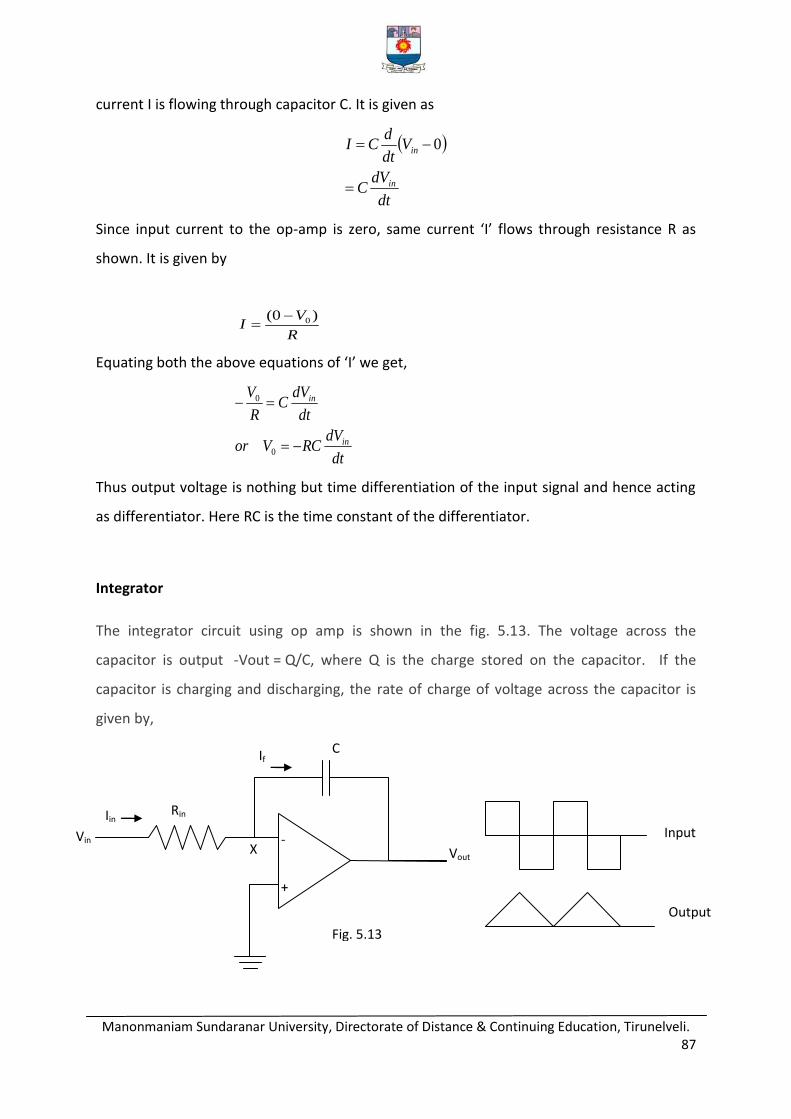
Manonmaniam Sundaranar University, Directorate of Distance & Continuing Education, Tirunelveli. 87
current I is flowing through capacitor C. It is given as
dt
dVC
Vdt
dCI
in
in
0
Since input current to the op-amp is zero, same current ‘I’ flows through resistance R as
shown. It is given by
R
VI
)0( 0
Equating both the above equations of ‘I’ we get,
dt
dVRCVor
dt
dVC
R
V
in
in
0
0
Thus output voltage is nothing but time differentiation of the input signal and hence acting
as differentiator. Here RC is the time constant of the differentiator.
Integrator
The integrator circuit using op amp is shown in the fig. 5.13. The voltage across the
capacitor is output -Vout = Q/C, where Q is the charge stored on the capacitor. If the
capacitor is charging and discharging, the rate of charge of voltage across the capacitor is
given by,
Vin
Rin
X
Iin
C
-
+
Vout
If
Fig. 5.13
Input
Output
wavefo
rm
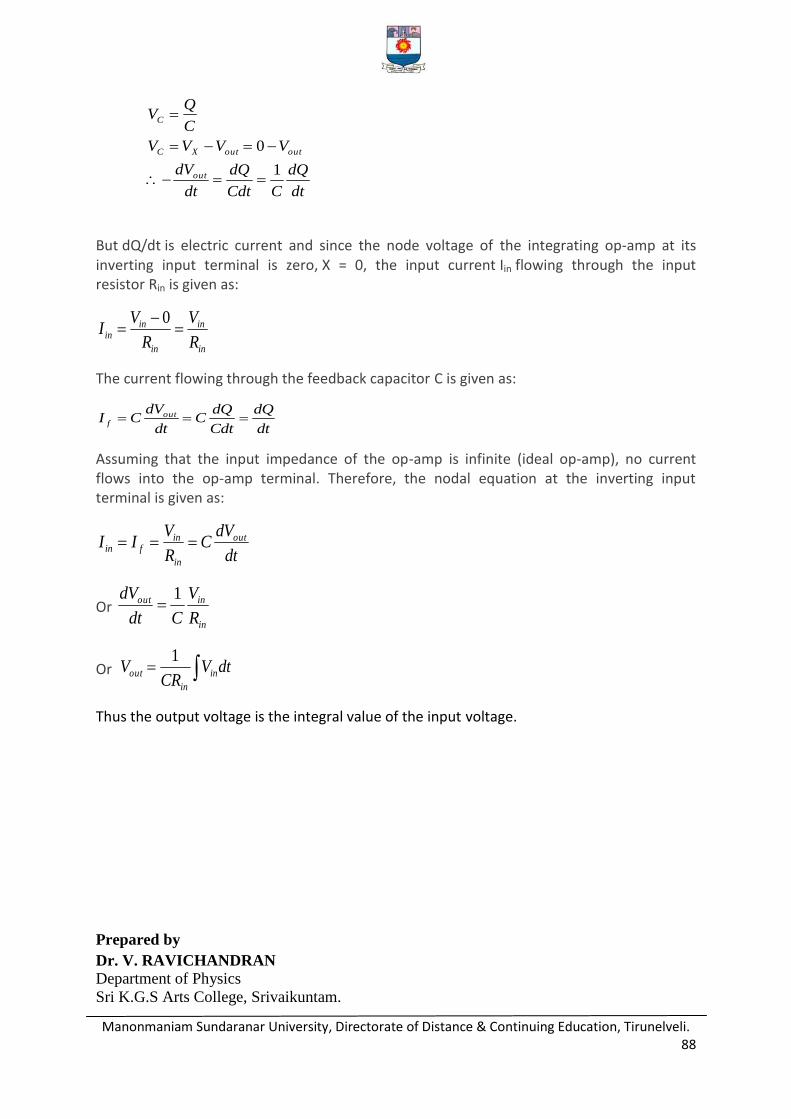
Manonmaniam Sundaranar University, Directorate of Distance & Continuing Education, Tirunelveli. 88
dt
dQ
CCdt
dQ
dt
dV
VVVV
C
QV
out
outoutXC
C
1
0
But dQ/dt is electric current and since the node voltage of the integrating op-amp at its inverting input terminal is zero, X = 0, the input current Iin flowing through the input resistor Rin is given as:
in
in
in
inin
R
V
R
VI
0
The current flowing through the feedback capacitor C is given as:
dt
dQ
Cdt
dQC
dt
dVCI out
f
Assuming that the input impedance of the op-amp is infinite (ideal op-amp), no current flows into the op-amp terminal. Therefore, the nodal equation at the inverting input terminal is given as:
dt
dVC
R
VII out
in
infin
Or in
inout
R
V
Cdt
dV 1
Or dtVCR
V in
in
out 1
Thus the output voltage is the integral value of the input voltage.
Prepared by
Dr. V. RAVICHANDRAN
Department of Physics
Sri K.G.S Arts College, Srivaikuntam.


![For B.Sc. [PHYSICS]](https://img.pdfslide.net/doc/110x75/627f3a5aed79f224f37a0636/for-bsc-physics.jpg)