Embed Size (px)
Citation preview
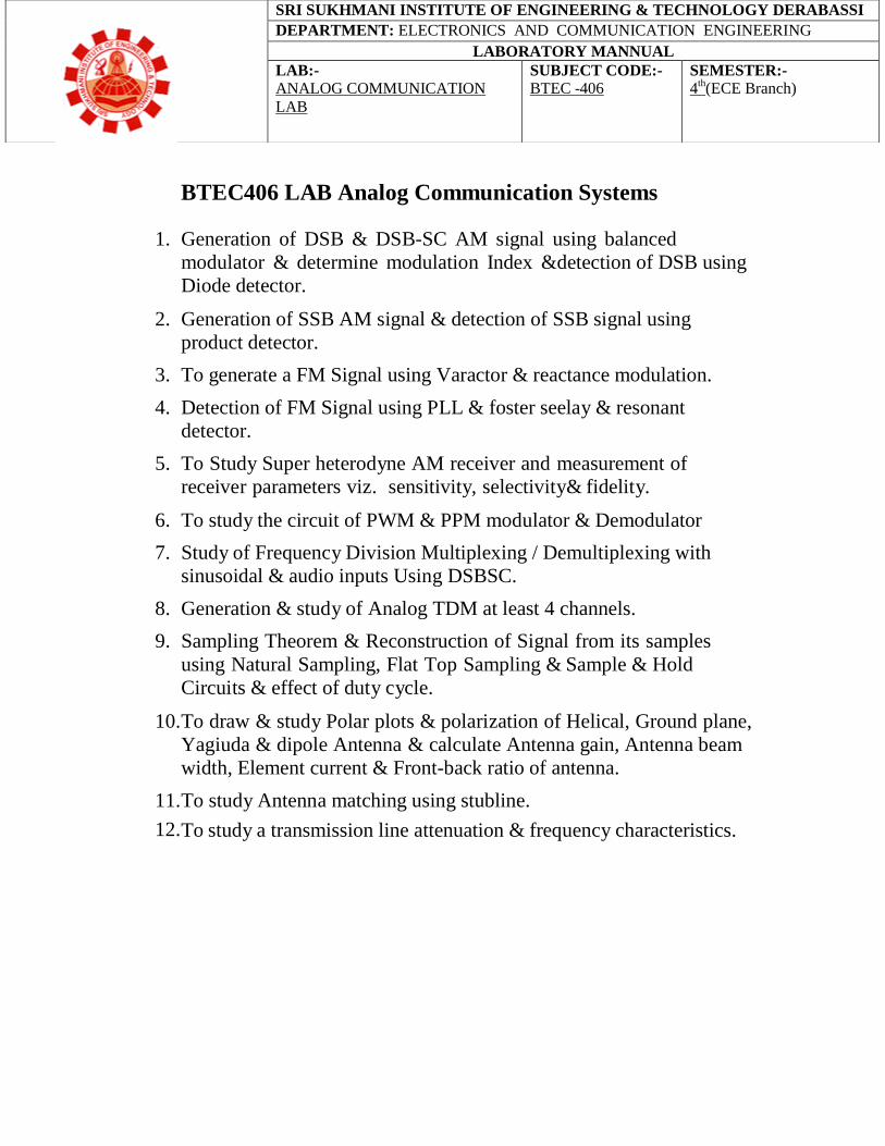
BTEC406 LAB Analog Communication Systems
1. Generation of DSB & DSB-SC AM signal using balanced
modulator & determine modulation Index &detection of DSB using
Diode detector.
2. Generation of SSB AM signal & detection of SSB signal using
product detector.
3. To generate a FM Signal using Varactor & reactance modulation.
4. Detection of FM Signal using PLL & foster seelay & resonant
detector.
5. To Study Super heterodyne AM receiver and measurement of
receiver parameters viz. sensitivity, selectivity& fidelity.
6. To study the circuit of PWM & PPM modulator & Demodulator
7. Study of Frequency Division Multiplexing / Demultiplexing with
sinusoidal & audio inputs Using DSBSC.
8. Generation & study of Analog TDM at least 4 channels.
9. Sampling Theorem & Reconstruction of Signal from its samples
using Natural Sampling, Flat Top Sampling & Sample & Hold
Circuits & effect of duty cycle.
10. To draw & study Polar plots & polarization of Helical, Ground plane,
Yagiuda & dipole Antenna & calculate Antenna gain, Antenna beam
width, Element current & Front-back ratio of antenna.
11. To study Antenna matching using stubline.
12. To study a transmission line attenuation & frequency characteristics.
SRI SUKHMANI INSTITUTE OF ENGINEERING & TECHNOLOGY DERABASSI
DEPARTMENT: ELECTRONICS AND COMMUNICATION ENGINEERING
LABORATORY MANNUAL
LAB:-
ANALOG COMMUNICATION
LAB
SUBJECT CODE:-
BTEC -406 SEMESTER:-
4th(ECE Branch)
EXPERIMENT-1
AIM:-Generation of DSB-SC signal using balanced modulator.
APPARATUS:-Balanced modulator kit, CRO, function generator.
THEORY:-
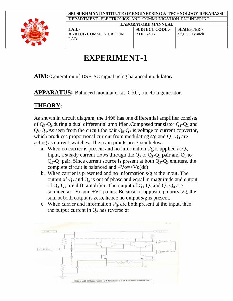
As shown in circuit diagram, the 1496 has one differential amplifier consists
of Q5-Q6 during a dual differential amplifier .Composed transistor Q1-Q2 and
Q3-Q4.As seen from the circuit the pair Q5-Q6 is voltage to current convertor,
which produces proportional current from modulating s/g and Q1-Q4 are
acting as current switches. The main points are given below:-
a. When no carrier is present and no information s/g is applied at Q5
input, a steady current flows through the Q5 to Q1-Q2 pair and Q6 to
Q3-Q4 pair. Since current source is present at both Q5-Q6 emitters, the
complete circuit is balanced and –Vo=+Vo(dc)
b. When carrier is presented and no information s/g at the input. The
output of Q2 and Q3 is out of phase and equal in magnitude and output
of Q3-Q4 are diff. amplifier. The output of Q1-Q3 and Q3-Q4 are
summed at –Vo and +Vo points. Because of opposite polarity s/g, the
sum at both output is zero, hence no output s/g is present.
c. When carrier and information s/g are both present at the input, then
the output current in Q6 has reverse of
SRI SUKHMANI INSTITUTE OF ENGINEERING & TECHNOLOGY DERABASSI
DEPARTMENT: ELECTRONICS AND COMMUNICATION ENGINEERING
LABORATORY MANNUAL
LAB:-
ANALOG COMMUNICATION
LAB
SUBJECT CODE:-
BTEC -406 SEMESTER:-
4th(ECE Branch)
Q5.Since it is also a amplifier. It has current in balance at the emitter of Q1-
Q2 and Q3-Q4 pair. In this case, the output of Q3-Q4 is higher than that of Q1-
Q2. At summing point, opposite polarity s/g are cancelled out and only
information s/g is obtained.
PROCEDURE:-
1. Make the connections as shown in circuit diagram.
2. Switch ON power supply and give the information s/g and carrier s/g
to the kit of DSB-SC balanced modulator.
3. Note the amplitude and frequency of modulating s/g as well as of the
modulated output signal from the CRO.
OBSERVATION TABLE:-
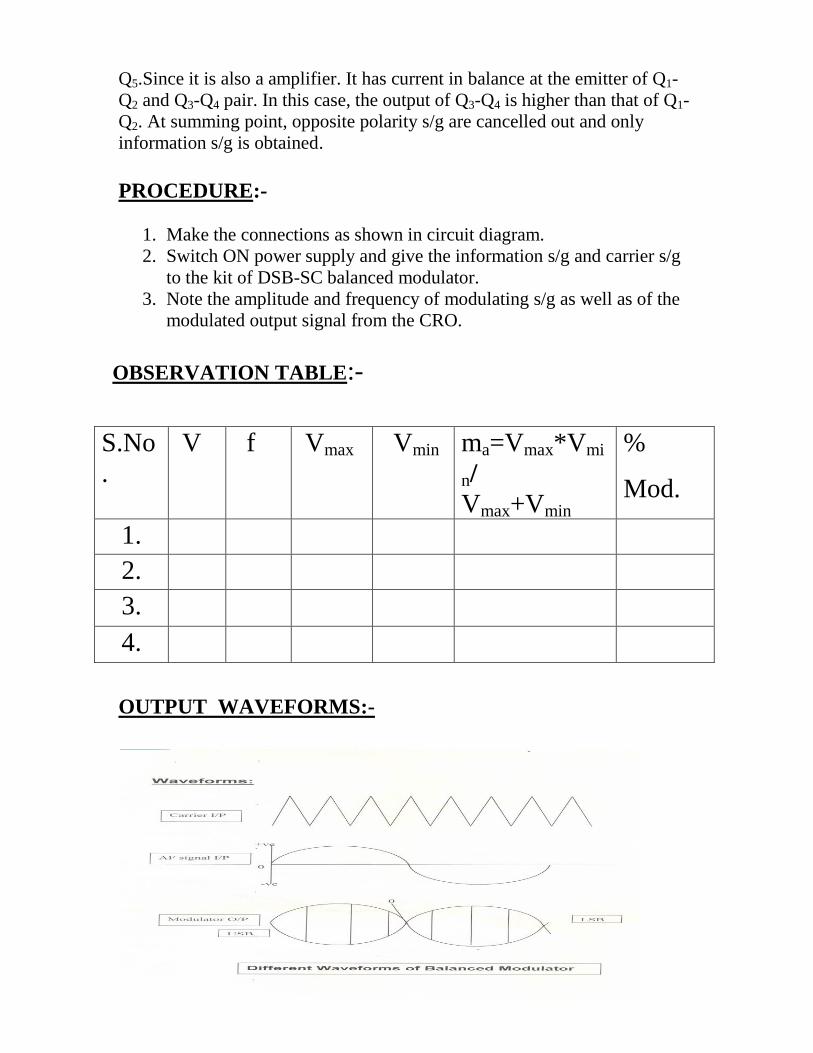
OUTPUT WAVEFORMS:-
S.No
.
V f Vmax Vmin ma=Vmax*Vmi
n/
Vmax+Vmin
%
Mod.
1.
2.
3.
4.
PRECAUTIONS:-
1. Connections should be tight.
2. Reading should be taken carefully and accurately.
RESULT:- The DSB-SC signal is generated using balanced modulator with ma=100%
EXPERIMENT NO-2
AIM:-Generation of SSB AM signal & detection using product detector.
APPARATUS:- SSB generation kit, connecting leads.
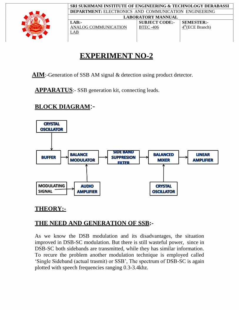
BLOCK DIAGRAM:-
THEORY:-
THE NEED AND GENERATION OF SSB:-
As we know the DSB modulation and its disadvantages, the situation
improved in DSB-SC modulation. But there is still wasteful power, since in
DSB-SC both sidebands are transmitted, while they has similar information.
To recure the problem another modulation technique is employed called
„Single Sideband (actual trasmit) or SSB‟, The spectrum of DSB-SC is again
plotted with speech frequencies ranging 0.3-3.4khz.
SRI SUKHMANI INSTITUTE OF ENGINEERING & TECHNOLOGY DERABASSI
DEPARTMENT: ELECTRONICS AND COMMUNICATION ENGINEERING
LABORATORY MANNUAL
LAB:-
ANALOG COMMUNICATION
LAB
SUBJECT CODE:-
BTEC -406 SEMESTER:-
4th(ECE Branch)
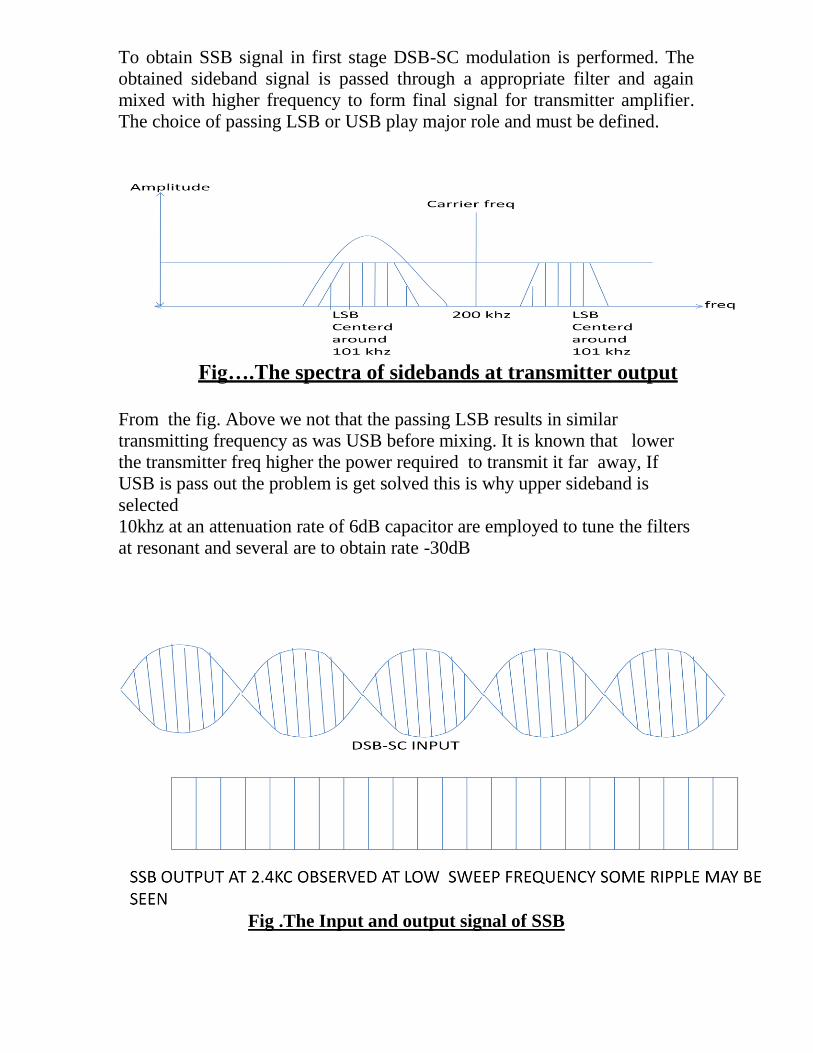
To obtain SSB signal in first stage DSB-SC modulation is performed. The
obtained sideband signal is passed through a appropriate filter and again
mixed with higher frequency to form final signal for transmitter amplifier.
The choice of passing LSB or USB play major role and must be defined.
Fig….The spectra of sidebands at transmitter output
From the fig. Above we not that the passing LSB results in similar
transmitting frequency as was USB before mixing. It is known that lower
the transmitter freq higher the power required to transmit it far away, If
USB is pass out the problem is get solved this is why upper sideband is
selected
10khz at an attenuation rate of 6dB capacitor are employed to tune the filters
at resonant and several are to obtain rate -30dB
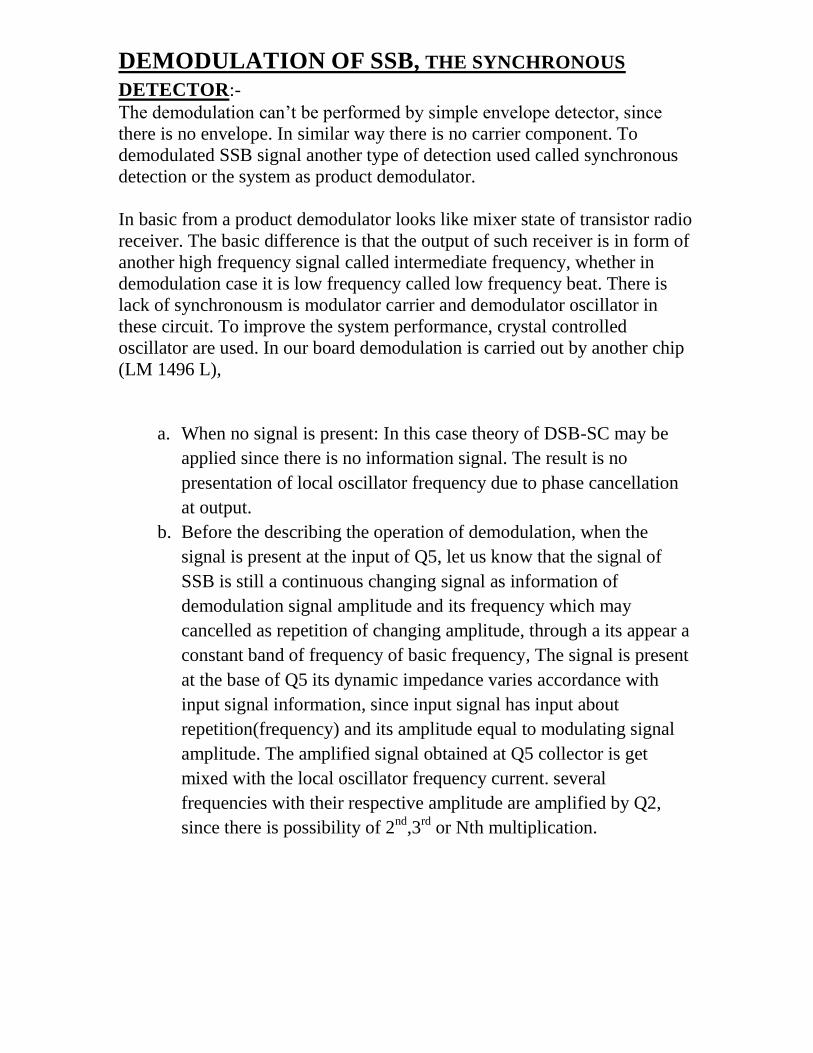
Fig .The Input and output signal of SSB
DEMODULATION OF SSB, THE SYNCHRONOUS
DETECTOR:-
The demodulation can‟t be performed by simple envelope detector, since
there is no envelope. In similar way there is no carrier component. To
demodulated SSB signal another type of detection used called synchronous
detection or the system as product demodulator.
In basic from a product demodulator looks like mixer state of transistor radio
receiver. The basic difference is that the output of such receiver is in form of
another high frequency signal called intermediate frequency, whether in
demodulation case it is low frequency called low frequency beat. There is
lack of synchronousm is modulator carrier and demodulator oscillator in
these circuit. To improve the system performance, crystal controlled
oscillator are used. In our board demodulation is carried out by another chip
(LM 1496 L),
a. When no signal is present: In this case theory of DSB-SC may be
applied since there is no information signal. The result is no
presentation of local oscillator frequency due to phase cancellation
at output.
b. Before the describing the operation of demodulation, when the
signal is present at the input of Q5, let us know that the signal of
SSB is still a continuous changing signal as information of
demodulation signal amplitude and its frequency which may
cancelled as repetition of changing amplitude, through a its appear a
constant band of frequency of basic frequency, The signal is present
at the base of Q5 its dynamic impedance varies accordance with
input signal information, since input signal has input about
repetition(frequency) and its amplitude equal to modulating signal
amplitude. The amplified signal obtained at Q5 collector is get
mixed with the local oscillator frequency current. several
frequencies with their respective amplitude are amplified by Q2,
since there is possibility of 2nd
,3rd
or Nth multiplication.
PROCEDURE:-
1. Switch „ON‟ the instrument using ON/OFF switch.
2. Connect the oscilloscope channel „A‟ across carrier oscillator socket
& ground socket and observe the wave shape.
3. Now connect the „A‟ channel across modulating signal output &
ground socket and observe the different frequency signal with
variation of set frequency knob .
4.Connect the circuit as shown in fig.
5.Now connect oscilloscope channel „B‟ across DSB-SC output and
adjust DSB to obtain nearly perfect signal‟
6.Now connect the oscilloscope channel „B‟ across SSB output and
measure the frequency find out which side band is obtain after filteration.
7.Now change the modulation signal and observe that output is decrease
and some band ripple is observe. Measure SSB output amplitude peak to
peak for each modulating frequency.
PRECAUTION:-
1. Connection should be tight.
2. Readings should be taken properly.
RESULT:-SSB signal is generated and demodulated.
EXPERIMENT NO-3
AIM:-To Generate a FM signal using Varactor & Reactance modulation.
APPARATUS:-FM generation kit, Connecting wires.
THEORY:-
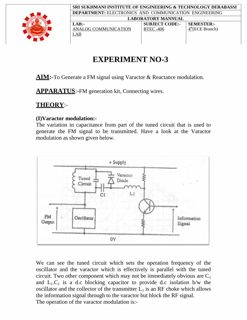
(I)Varactor modulation:-
The variation in capacitance from part of the tuned circuit that is used to
generate the FM signal to be transmitted. Have a look at the Varactor
modulation as shown given below.
We can see the tuned circuit which sets the operation frequency of the
oscillator and the varactor which is effectively is parallel with the tuned
circuit. Two other component which may not be immediately obvious are C1
and L1.C1 is a d.c blocking capacitor to provide d.c isolation b/w the
oscillator and the collector of the transmitter L1 is an RF choke which allows
the information signal through to the varactor but block the RF signal.
The operation of the varactor modulation is:-
SRI SUKHMANI INSTITUTE OF ENGINEERING & TECHNOLOGY DERABASSI
DEPARTMENT: ELECTRONICS AND COMMUNICATION ENGINEERING
LABORATORY MANNUAL
LAB:-
ANALOG COMMUNICATION
LAB
SUBJECT CODE:-
BTEC -406 SEMESTER:-
4th(ECE Branch)
1. The information signal is applied to the base of the input transistor
and appear amplifier and inverted at the collector.
2. This allow the frequency pass through RF choke and is a applied
across varactor diode.
3. The varactor diode change its capacitance is sympathy with the
information signal and therefore changes to the total value of the
capacitance in the tuned circuit.
4. The changing value of capacitance causes the oscillation frequency to
increase & decrease under the control of information signal.
Before we start of the varactor/reactance modulation technique we
shell study a simple VCO circuit.
Simply connect the output to the socket labeled VCO modulation in
and observe the FM modulated waveform on the oscilloscope at the
VCO modulation out terminal. Keep the amplitude of audio output to
approx 4v p-p and frequency 2Khz approx observe a stable FM
modulated waveform on CRO. This should look like as under similar
waveforms as shown below,
Now disconnect the audio amplifier‟s output from modulation IN and
connect it to audio IN, keep the reactance/vibrator switch in varactor
position. Observe the output of mixer/amplifier circuit keep the
oscilloscope in X 10 position now observe the full waveform by
shifting the X position.
The resemblance b/w the output of VCO and varactor modulator are
same.
The frequency modulation in VCO was more because the frequency
difference/w the carrier and the modulating signal was very less. But
in real life application reactance and varactor modulating techniques
are used which utilizes high frequency carrier and you will not
observe signal.
PROCEDURE:-
1. Ensure that the following initial condition exist on ME 770‟s
All switched faults off.
Amplitude pot(in mixer amplifier block)in fully clockwise
direction.
VOC switch(in phase locked loop detector block)in OFF
position.
2. Make a connection as shown in figure.
3. Switch ON the power.
4. Turn the audio oscillator blocks amplitude port its fully clockwise
position and the examine the blocks output t.p.1 on the oscilloscope.
This is audio frequency sine wave which will be used as a modulation
signal note that the sine wave‟s frequency can be adjusted from about
300 Hz to approximately 3.4 Khz by adjusted the audio oscillator
frequency port.
5. Connect the output socket of the audio oscillator block to the audio
input socket of the modulation circuit block.
6. Set the varactor/reactance switch to the varactor position. This switch
select the varactor modulation also disables the reactance modulator to
prevent any interference b/w two circuits.
7. Put the varactor modulator‟s carrier frequency port in its midway
position, and then examine TP 34.Note that it is sine wave of
approximately 1.2vp-p centered on 0 v.
8. The amplitude of FM carrier is adjustable by means of mixer/amplifier
block‟s amplitude port from the zero to its hot level. Try turning this
port slowly anticlockwise, and note the amplitude of the FM signal
can be reduced to zero. Return the amplitude port to its fully
clockwise position.
9. Try varying the carrier frequency port and observe the effect.
10. Also see the effect of varying the amplitude and frequency port in
the audio oscillator block.
11. Turn the carrier frequency port in the varactor modulator block slowly
clockwise and note that in addition to the carrier frequency increase
there is decrease in the amount of frequency deviation that is present.
12. Return the carrier frequency port to its middle position and monitor
the audio input and FM output triggering the oscilloscope on the audio
input signal. Turn the audio oscillator amplitude port through its range
of adjustment and note the amplitude of FM output signal does not
change.
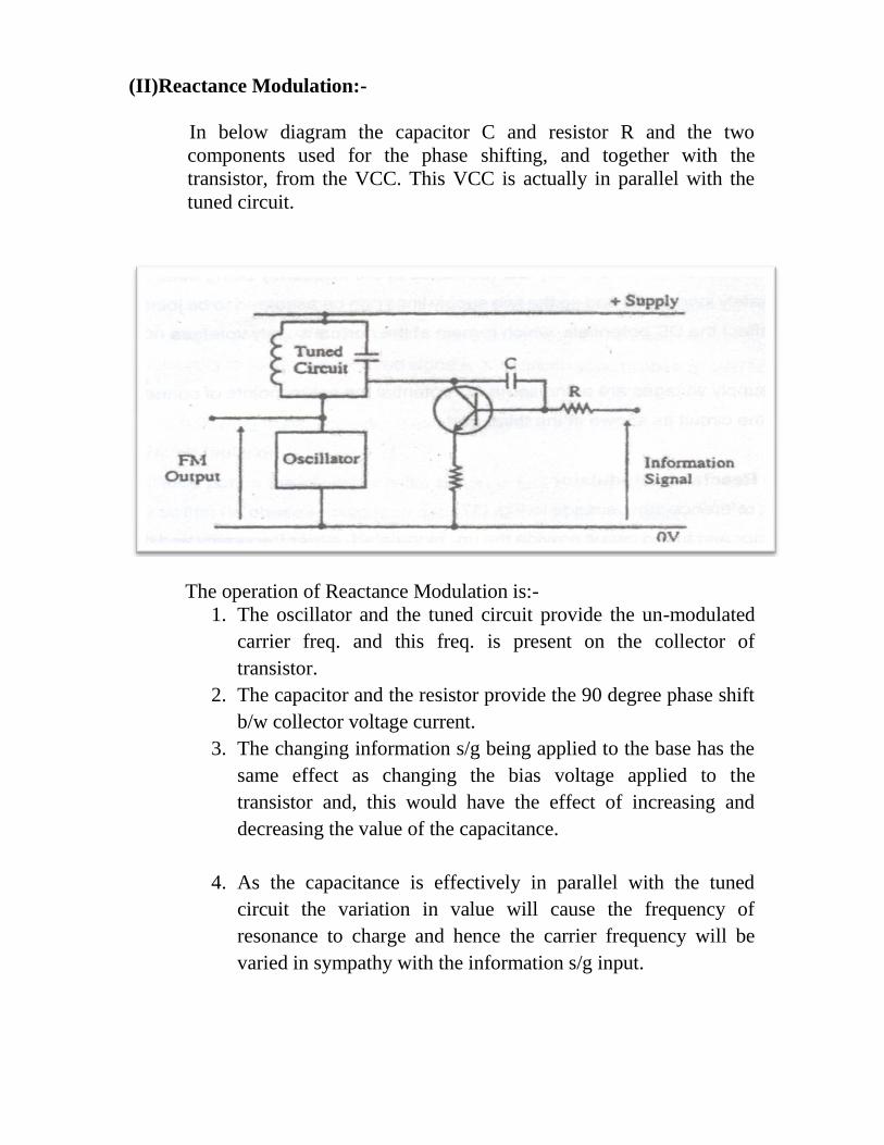
(II)Reactance Modulation:-
In below diagram the capacitor C and resistor R and the two
components used for the phase shifting, and together with the
transistor, from the VCC. This VCC is actually in parallel with the
tuned circuit.
The operation of Reactance Modulation is:-
1. The oscillator and the tuned circuit provide the un-modulated
carrier freq. and this freq. is present on the collector of
transistor.
2. The capacitor and the resistor provide the 90 degree phase shift
b/w collector voltage current.
3. The changing information s/g being applied to the base has the
same effect as changing the bias voltage applied to the
transistor and, this would have the effect of increasing and
decreasing the value of the capacitance.
4. As the capacitance is effectively in parallel with the tuned
circuit the variation in value will cause the frequency of
resonance to charge and hence the carrier frequency will be
varied in sympathy with the information s/g input.
PROCEDURE:-
1. The first six steps are same as that of Varactor Modulation,
2. The output s/g from the reactance modulator block appear at
TP13,before being buffered and amplified by the amplifier block. At
TP13 the capacitive loading affect may slightly affect the modulator‟s
output frequency.
3. In order to avoid this problem we will monitor the buffered FM output
s/g from the amplifier block.
4. Put the Reactance Modulator‟s pot in its midway position then examine
TP34.
5. The amplitude of FM carrier is adjustable by means of the amplifier
block‟s amplitude pot, from zero to its present level. Try turning this pot
slowly anticlockwise, and note that the amplitude of the FM s/g can be
reduced to zero.
6. The frequency of the FM s/g should be approximately 455khz at the
moment. This carrier frequency can be varied from 453khz to 460khz
by adjusting the carrier frequency in the reactance modulator block.
7. This step is same as that of 6th
step of Varactor Modulation.
8. Monitor the audio input(TP6) and FM output(TP34) triggering the
oscilloscope on the audio input s/g. Turn the audio oscillator‟s
amplitude pot throughout its range of adjustment and note that the
amplitude of the FM output s/g does not change.
RESULT:-The FM signal is generated using Varactor and Reactance
Modulation.
PRECAUTION:-
1.Connection should be tight.
2.Readings should be taken properly.
EXPERIMENT-4
AIM:- To study frequency demodulation using detuned resonant circuit
detector, phase lock loop, foster seeley detector.
APPARATUS:- frequency demodulation kit, cro, connecting lead.
THEORY:-
An frequency receiver is a very similar to an AM receiver. The most
significant change is that the demodulation must now extract the
information signal from a frequency rather than amplitude modulation
wave. The basic requirement of frequency demodulation is therefore
to convert frequency changes into change in voltage, with a minimum
amount of distortion.
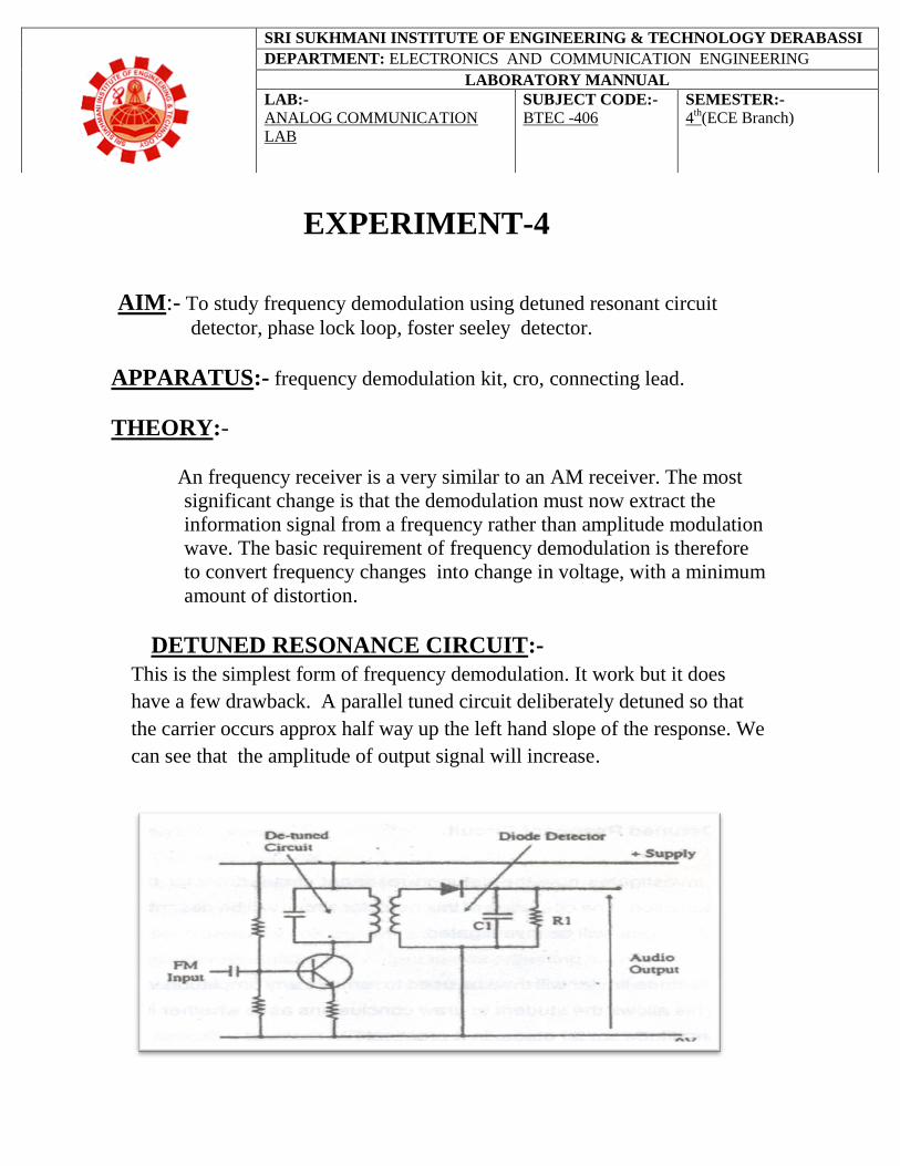
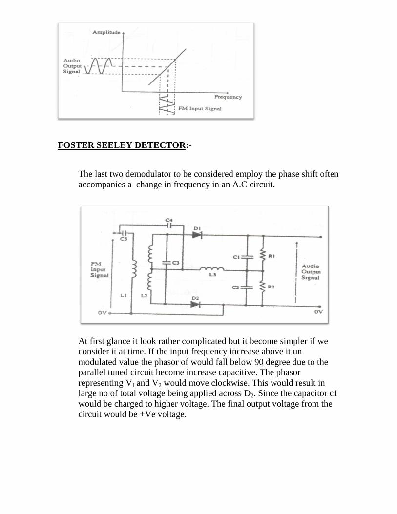
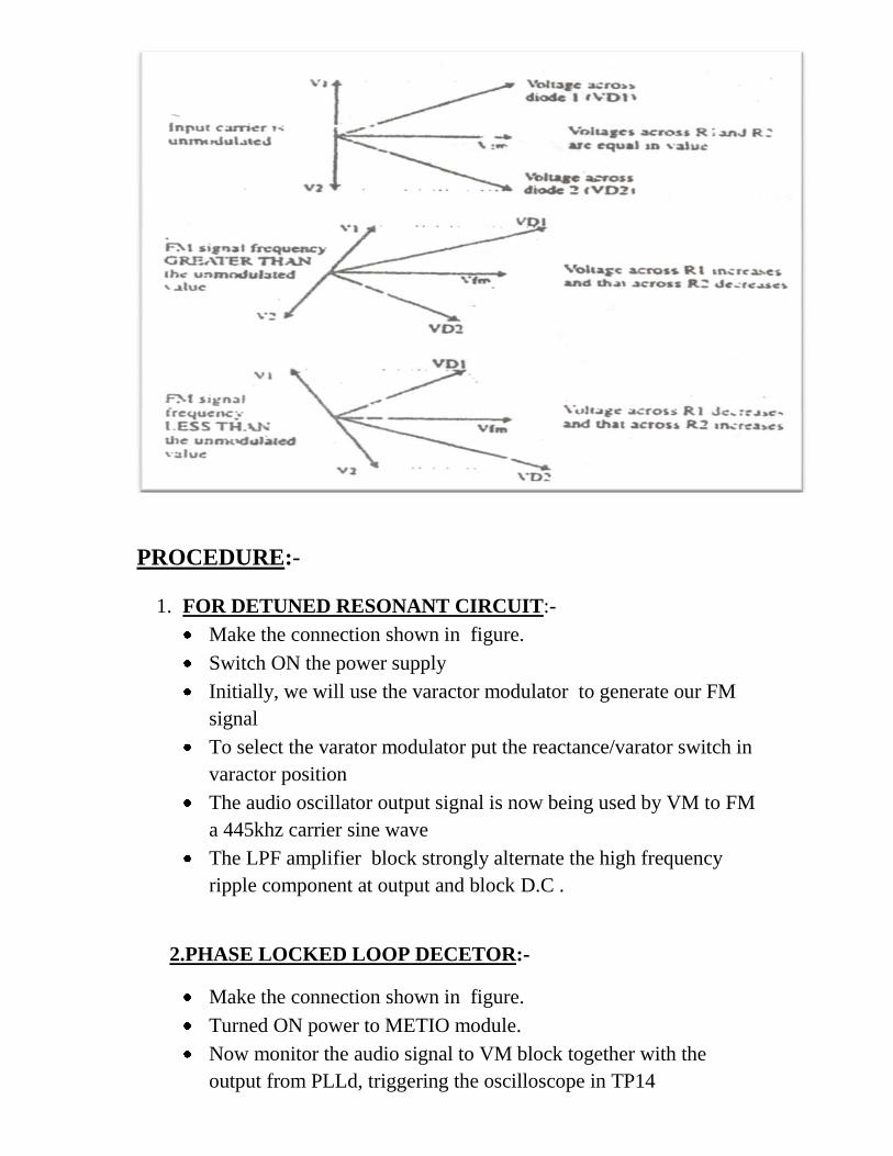
DETUNED RESONANCE CIRCUIT:-
This is the simplest form of frequency demodulation. It work but it does
have a few drawback. A parallel tuned circuit deliberately detuned so that
the carrier occurs approx half way up the left hand slope of the response. We
can see that the amplitude of output signal will increase.
SRI SUKHMANI INSTITUTE OF ENGINEERING & TECHNOLOGY DERABASSI
DEPARTMENT: ELECTRONICS AND COMMUNICATION ENGINEERING
LABORATORY MANNUAL
LAB:-
ANALOG COMMUNICATION
LAB
SUBJECT CODE:-
BTEC -406 SEMESTER:-
4th(ECE Branch)
Decrease as the input frequency changes. For example , if the frequency of
the incoming signal were increase, the operating point would move toward
the right on diagram. This will cause an increase in the amplitude of output
signal. A fm signal at the output it is really that simple.
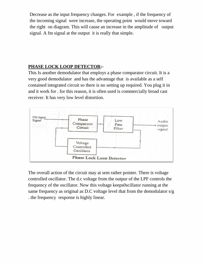
PHASE LOCK LOOP DETECTOR:-
This Is another demodulator that employs a phase comparator circuit. It is a
very good demodulator and has the advantage that is available as a self
contained integrated circuit so there is no setting up required. You plug it in
and it work for . for this reason, it is often used is commercially broad cast
receiver. It has very low level distortion.
The overall action of the circuit may at sem rather pointer. There is voltage
controlled oscillator. The d.c voltage from the outpur of the LPF controls the
frequency of the oscillator. Now this voltage keeps0scillator running at the
same frequency as original as D.C voltage level that from the demodulator s/g
. the frequency response is highly linear.
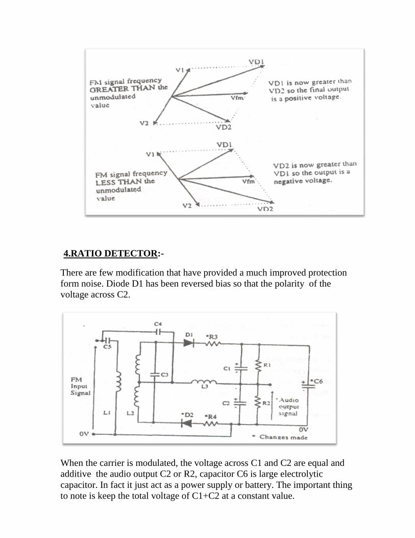
FOSTER SEELEY DETECTOR:-
The last two demodulator to be considered employ the phase shift often
accompanies a change in frequency in an A.C circuit.
At first glance it look rather complicated but it become simpler if we
consider it at time. If the input frequency increase above it un
modulated value the phasor of would fall below 90 degree due to the
parallel tuned circuit become increase capacitive. The phasor
representing V1 and V2 would move clockwise. This would result in
large no of total voltage being applied across D2. Since the capacitor c1
would be charged to higher voltage. The final output voltage from the
circuit would be +Ve voltage.
4.RATIO DETECTOR:-
There are few modification that have provided a much improved protection
form noise. Diode D1 has been reversed bias so that the polarity of the
voltage across C2.
When the carrier is modulated, the voltage across C1 and C2 are equal and
additive the audio output C2 or R2, capacitor C6 is large electrolytic
capacitor. In fact it just act as a power supply or battery. The important thing
to note is keep the total voltage of C1+C2 at a constant value.
PROCEDURE:-
1. FOR DETUNED RESONANT CIRCUIT:-
Make the connection shown in figure.
Switch ON the power supply
Initially, we will use the varactor modulator to generate our FM
signal
To select the varator modulator put the reactance/varator switch in
varactor position
The audio oscillator output signal is now being used by VM to FM
a 445khz carrier sine wave
The LPF amplifier block strongly alternate the high frequency
ripple component at output and block D.C .
2.PHASE LOCKED LOOP DECETOR:-
Make the connection shown in figure.
Turned ON power to METIO module.
Now monitor the audio signal to VM block together with the
output from PLLd, triggering the oscilloscope in TP14
The LPF/amplifier bloks strongly alternate the high freq. ripple
component at the detector output and also bloks D.C
Adjust the audio oscillator block‟s amplitude and freboost and
compare the original audio signal with the final demodulator
signal.
2. FOR RATIO DETECTOR:-
Make the connection shown in figure
Turned ON power of module.
Now monitor the input signal to the VM block together with the
ratio output from the ratio detector block triggering the oscillator
on TP 14 . The signal at TP 53 should be connection two main
component.
The LPF/amplifier block removed the D.C offset voltage at the
detector output. Strongly attenuates any residual high freq. ripple
may be present.
Monitor the audio input to the VM and the output of the LPF and
adjust the gain point until the amplifier the modulated output
wave form.
Adjust the audio oscillator blocks amplitude and frequency
component and compare the original signal with the demodulated
signal.
3. FOR FOSTER SEELEY DETECTOR:-
Make the connection shown in figure
Turned ON power of module.
We will use the VM to generate FM signal since this is more
linear of the two modulators as fact as its freq. /voltage
characteristic is.
Now monitor audio input signal to the VM block together with the
foster seeley /ratio detector block triggering the oscilloscope on
TP 14.
PRECAUTION:-
Connection should be tight.
Readings must be taken carefully.
RESULT:- Frequency demodulated s/g is generated using detuned resonant
circuit detector, phase lock loop, foster seeley detector.
]
EXPERIMENT-6
AIM:-To generate the pulse width & Pulse position modulated and
demodulated signals
APPARATUS-: 1. Pulse width modulation and Demodulation Trainer. 2. CRO 3. BNC probes and Connecting Wires
THEORY:-
PWM:-In PWM, the samples of the message signal are used to vary the
duration of the individual pulses. Width may be varied by varying the
time of occurrence of leading edge, the trailing edge or both the edges of
the pulse in accordance with modulating wave. It is also called Pulse
Duration Modulation.
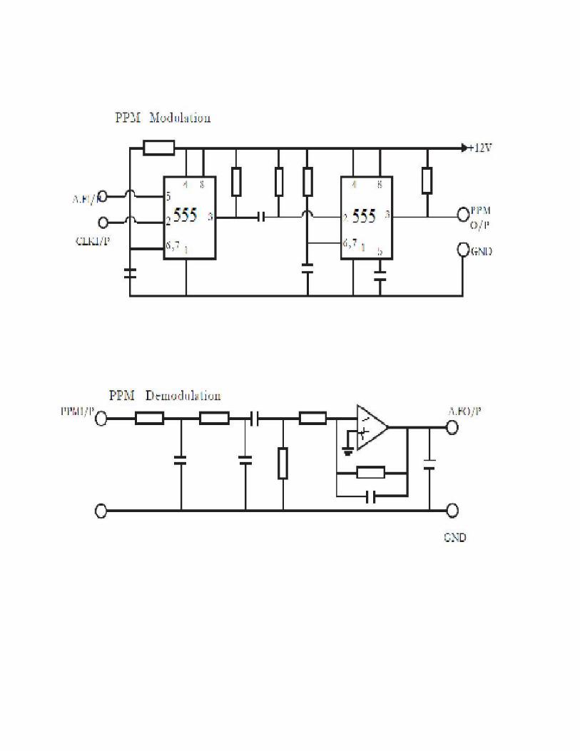
PPM:-In Pulse Position Modulation, both the pulse amplitude and pulse duration are held constant but the position of the pulse is varied in proportional to the sampled values of the message signal. Pulse time modulation is a class of signaling technique that encodes the sample values of an analog signal on to the time axis of a digital signal and it is analogous to angle modulation techniques. The two main types PTM are PWM and PPM. In PPM the analog sample value determines the position of a narrow pulse relative to the clocking time. In PPM rise time of pulse decides the channel bandwidth. It has low noise interference
SRI SUKHMANI INSTITUTE OF ENGINEERING & TECHNOLOGY DERABASSI
DEPARTMENT: ELECTRONICS AND COMMUNICATION ENGINEERING
LABORATORY MANNUAL
LAB:-
ANALOG COMMUNICATION
LAB
SUBJECT CODE:-
BTEC -406 SEMESTER:-
4th(ECE Branch)
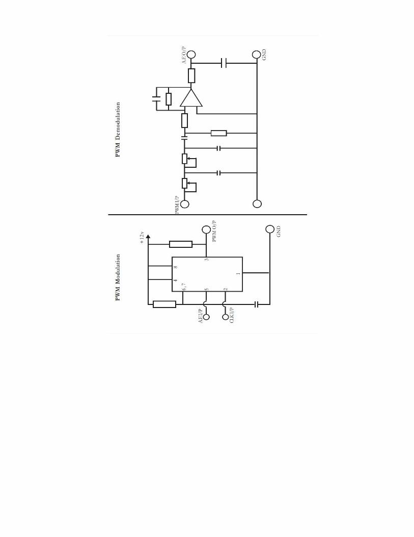
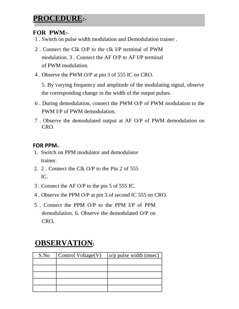
PROCEDURE:-
FOR PWM:-
1 . Switch on pulse width modulation and Demodulation trainer . 2 . Connect the Clk O/P to the clk I/P terminal of PWM
modulation. 3 . Connect the AF O/P to AF I/P terminal
of PWM modulation. 4 . Observe the PWM O/P at pin 3 of 555 IC on CRO.
5. By varying frequency and amplitude of the modulating signal, observe
the corresponding change in the width of the output pulses. 6 . During demodulation, connect the PWM O/P of PWM modulation to the
PWM I/P of PWM demodulation. 7 . Observe the demodulated output at AF O/P of PWM demodulation on
CRO.
FOR PPM:-
1. Switch on PPM modulator and demodulator
trainer.
2. 2 . Connect the Clk O/P to the Pin 2 of 555
IC. 3 . Connect the AF O/P to the pin 5 of 555 IC. 4 . Observe the PPM O/P at pin 3 of second IC 555 on CRO. 5 . Connect the PPM O/P to the PPM I/P of PPM
demodulation. 6. Observe the demodulated O/P on
CRO.
OBSERVATION:
S.No Control Voltage(V) o/p pulse width (msec)
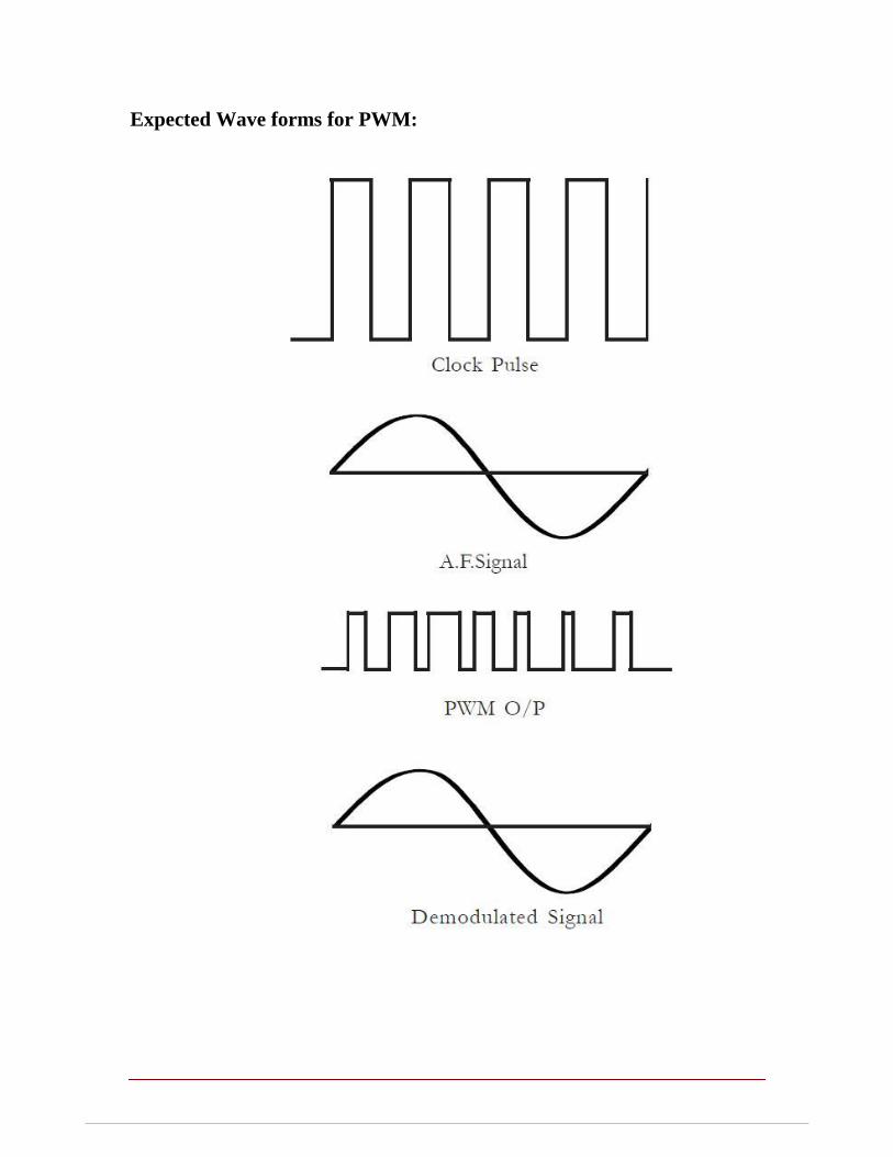
Expected Wave forms for PWM:
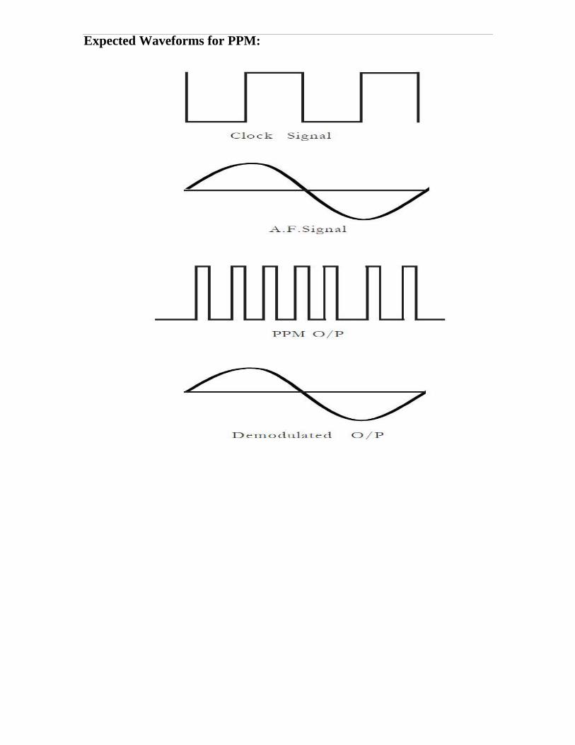
Expected Waveforms for PPM:
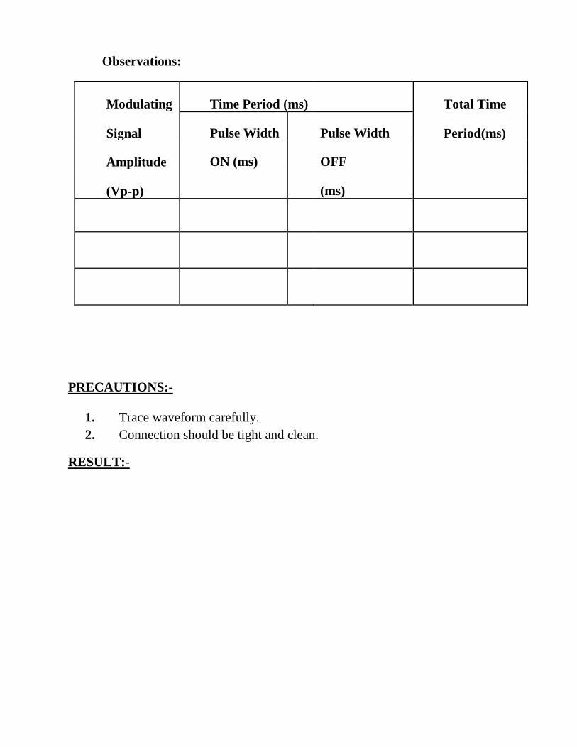
Observations:
Modulating Time Period (ms) Total Time
Signal Pulse Width Pulse Width Period(ms)
Amplitude ON (ms) OFF
(Vp-p) (ms)
PRECAUTIONS:-
1. Trace waveform carefully.
2. Connection should be tight and clean.
RESULT:-
EXPERIMENT-7
AIM:-To study of frequency division multiplexing / demultiplexing with
sinusoidal and audio input using DSB-SC.
APPARATUS:-Frequency division Multiplexing/ Demultiplexing kit,
connecting wires.
THEORY:-
Multiplexing means sending of number of separate s/g together over the same
number of wire simultaneously without interference.
(I)FDM:-In FDM system the transmission bandwidth is divided b/w various use as
shown in below figure:
SRI SUKHMANI INSTITUTE OF ENGINEERING & TECHNOLOGY DERABASSI
DEPARTMENT: ELECTRONICS AND COMMUNICATION ENGINEERING
LABORATORY MANNUAL
LAB:-
ANALOG COMMUNICATION
LAB
SUBJECT CODE:-
BTEC -406 SEMESTER:-
4th(ECE Branch)
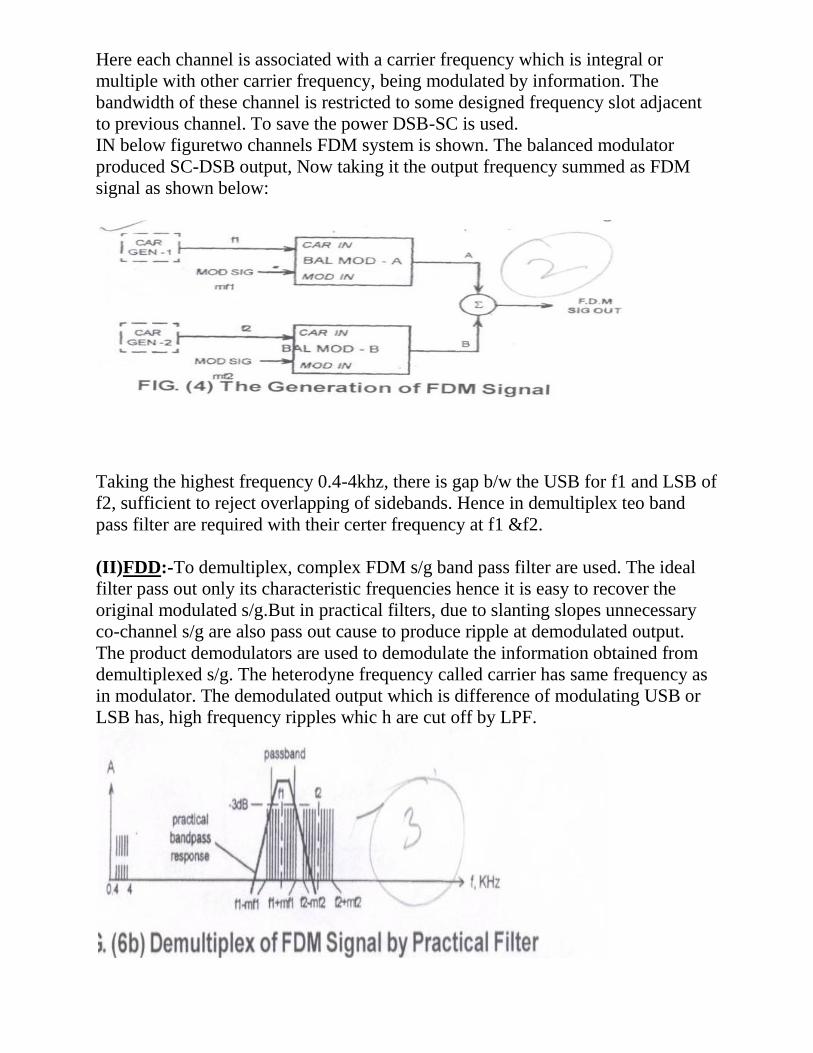
Here each channel is associated with a carrier frequency which is integral or
multiple with other carrier frequency, being modulated by information. The
bandwidth of these channel is restricted to some designed frequency slot adjacent
to previous channel. To save the power DSB-SC is used.
IN below figuretwo channels FDM system is shown. The balanced modulator
produced SC-DSB output, Now taking it the output frequency summed as FDM
signal as shown below:
Taking the highest frequency 0.4-4khz, there is gap b/w the USB for f1 and LSB of
f2, sufficient to reject overlapping of sidebands. Hence in demultiplex teo band
pass filter are required with their certer frequency at f1 &f2.
(II)FDD:-To demultiplex, complex FDM s/g band pass filter are used. The ideal
filter pass out only its characteristic frequencies hence it is easy to recover the
original modulated s/g.But in practical filters, due to slanting slopes unnecessary
co-channel s/g are also pass out cause to produce ripple at demodulated output.
The product demodulators are used to demodulate the information obtained from
demultiplexed s/g. The heterodyne frequency called carrier has same frequency as
in modulator. The demodulated output which is difference of modulating USB or
LSB has, high frequency ripples whic h are cut off by LPF.
PROCEDURE:-
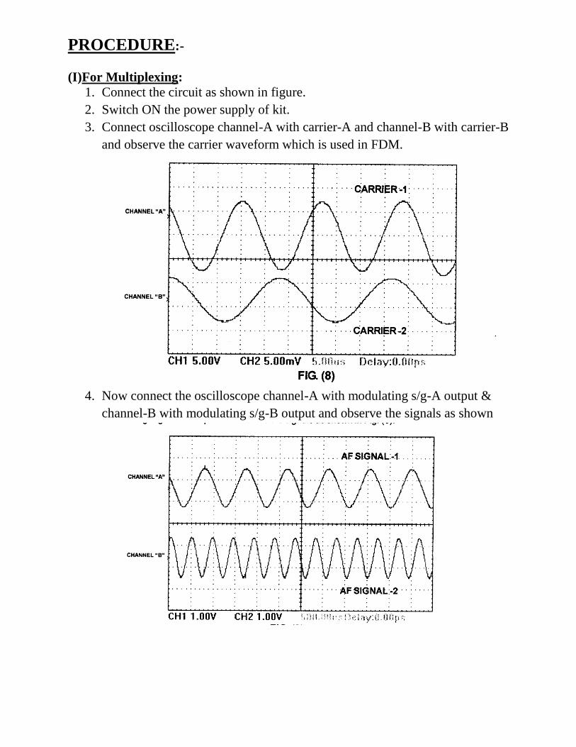
(I)For Multiplexing:
1. Connect the circuit as shown in figure.
2. Switch ON the power supply of kit.
3. Connect oscilloscope channel-A with carrier-A and channel-B with carrier-B
and observe the carrier waveform which is used in FDM.
4. Now connect the oscilloscope channel-A with modulating s/g-A output &
channel-B with modulating s/g-B output and observe the signals as shown
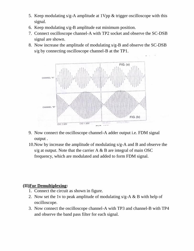
5. Keep modulating s/g-A amplitude at 1Vpp & trigger oscilloscope with this
signal.
6. Keep modulating s/g-B amplitude eat minimum position.
7. Connect oscilloscope channel-A with TP2 socket and observe the SC-DSB
signal are shown.
8. Now increase the amplitude of modulating s/g-B and observe the SC-DSB
s/g by connecting oscilloscope channel-B at the TP1.
9. Now connect the oscilloscope channel-A adder output i.e. FDM signal
output .
10.Now by increase the amplitude of modulating s/g-A and B and observe the
s/g at output. Note that the carrier A & B are integral of main OSC
frequency, which are modulated and added to form FDM signal.
(II)For Demultiplexing:
1. Connect the circuit as shown in figure.
2. Now set the 1v to peak amplitude of modulating s/g-A & B with help of
oscilloscope.
3. Now connect the oscilloscope channel-A with TP3 and channel-B with TP4
and observe the band pass filter for each signal.
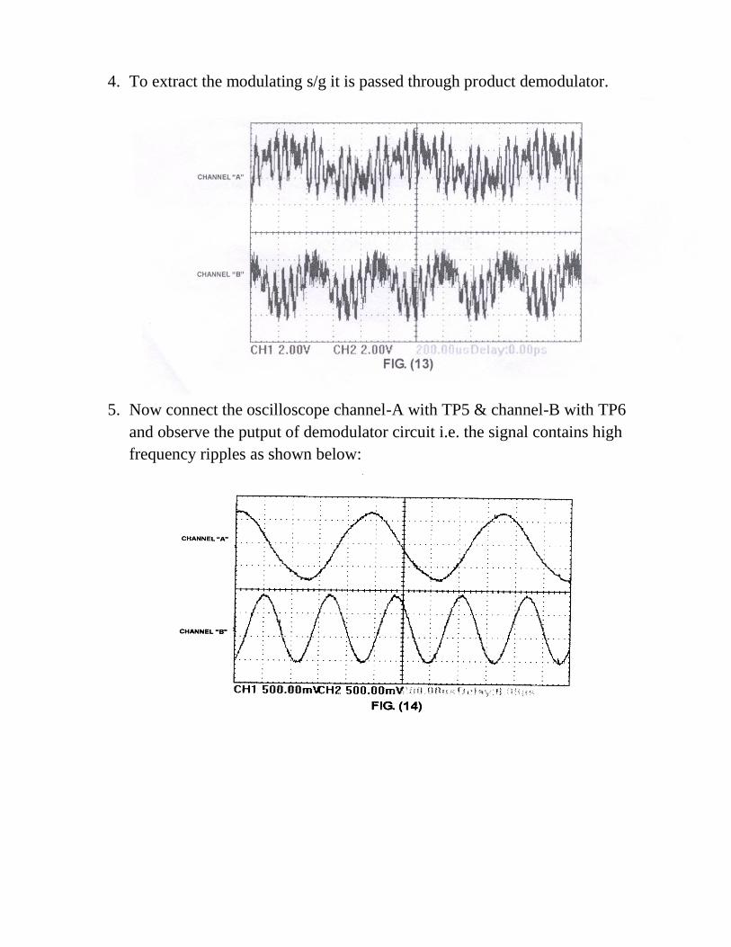
4. To extract the modulating s/g it is passed through product demodulator.
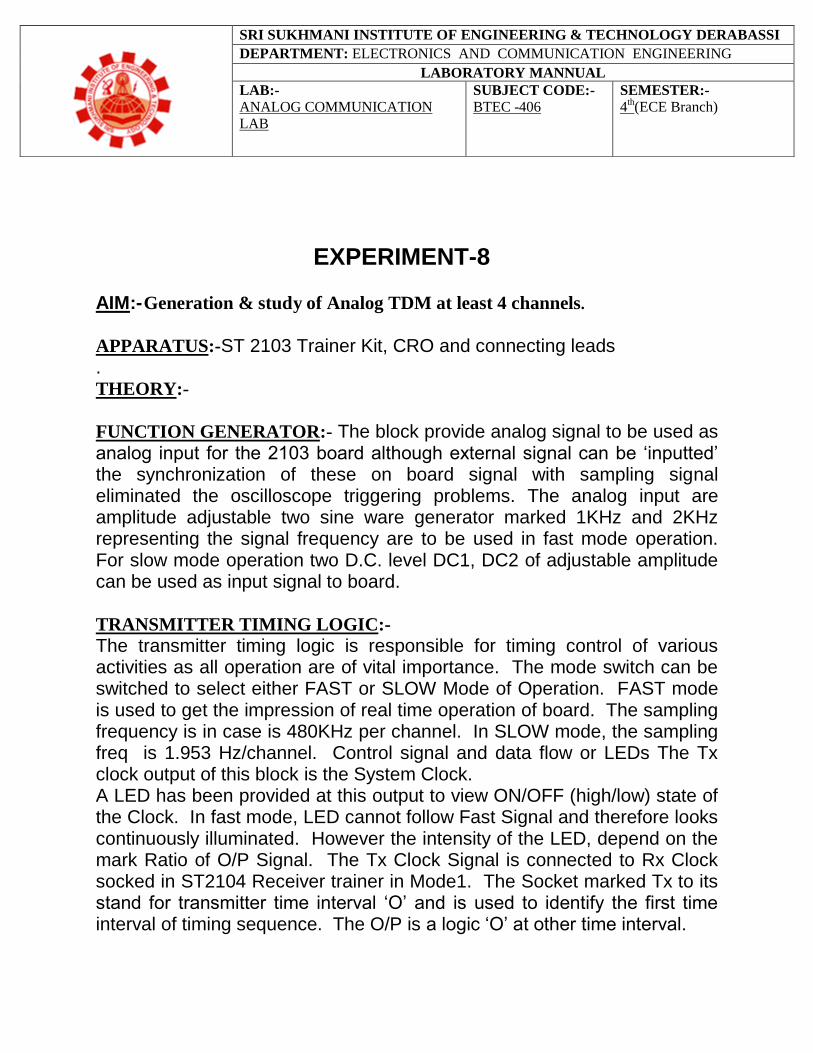
5. Now connect the oscilloscope channel-A with TP5 & channel-B with TP6
and observe the putput of demodulator circuit i.e. the signal contains high
frequency ripples as shown below:

PRECAUTIONS:-
1. Connections should be tight.
2. Reading should be taken properly.
RESULT:-
EXPERIMENT-8 AIM:- Generation & study of Analog TDM at least 4 channels. APPARATUS:-ST 2103 Trainer Kit, CRO and connecting leads . THEORY:-
FUNCTION GENERATOR:- The block provide analog signal to be used as analog input for the 2103 board although external signal can be ‘inputted’ the synchronization of these on board signal with sampling signal eliminated the oscilloscope triggering problems. The analog input are amplitude adjustable two sine ware generator marked 1KHz and 2KHz representing the signal frequency are to be used in fast mode operation. For slow mode operation two D.C. level DC1, DC2 of adjustable amplitude can be used as input signal to board. TRANSMITTER TIMING LOGIC:-
The transmitter timing logic is responsible for timing control of various activities as all operation are of vital importance. The mode switch can be switched to select either FAST or SLOW Mode of Operation. FAST mode is used to get the impression of real time operation of board. The sampling frequency is in case is 480KHz per channel. In SLOW mode, the sampling freq is 1.953 Hz/channel. Control signal and data flow or LEDs The Tx clock output of this block is the System Clock. A LED has been provided at this output to view ON/OFF (high/low) state of the Clock. In fast mode, LED cannot follow Fast Signal and therefore looks continuously illuminated. However the intensity of the LED, depend on the mark Ratio of O/P Signal. The Tx Clock Signal is connected to Rx Clock socked in ST2104 Receiver trainer in Mode1. The Socket marked Tx to its stand for transmitter time interval ‘O’ and is used to identify the first time interval of timing sequence. The O/P is a logic ‘O’ at other time interval.
SRI SUKHMANI INSTITUTE OF ENGINEERING & TECHNOLOGY DERABASSI
DEPARTMENT: ELECTRONICS AND COMMUNICATION ENGINEERING
LABORATORY MANNUAL
LAB:-
ANALOG COMMUNICATION
LAB
SUBJECT CODE:-
BTEC -406 SEMESTER:-
4th(ECE Branch)
It is used to establish synchronization is Mode 1 is selected. In this mode it is connected to Rx. To socked in ST2104 Receiver trainer A LED has been provided to view the signal in slow mode. Sampling unit:- This unit convert the analog Input Signal to the PAM Signal and then multiplex them in time domain. The sampling of two channel CHO & CH1 can be observed with LED marked CHO sampled in fast mode, CH1 samples in slow mode. A/D CONVERTOR BLOCK:- In this block the time division Multiplexed analog PAM Signal are digitally coded. The operation of this unit is controlled by signal from transmitter timing logic block named SC which indicated Start of Conversion(SC). The signal can be visually observed by LED illumination is slow mode. The EC signal is output of A/D Converter Circuit indicating END OF CONVERSION. The PCM word is then clocked into latched drives which drive LEDs indicating the bit status as output word. PARALLEL TO SERIES CONVERTOR (Shift Register):- The O/P from A/D Converter is in parallel format which must be converted into a serial format prior to transmission through cable etc. This process is called parallel to Serial Convertor. It is performed by two 4-bit Shift Register. The S/L Signal is output from the transmitter timing block and indicate where the data is being loaded or shifter in Shift Register. Output Logic Block:- The block ensures that the Shift PCM data from two analog input channel and output from the Sync. Code generator are routed through the output of STZ103. Transmitter trainer at the correct cycle in the block so as the let the data settle down due to spurious transmission before transmitted. The final O/P marked ‘PCMOUTAT’ is thus the coded version of the analog Input along with Sync. Code multiplexed in time domain and delayed of half clock cycle. Each new data bit appear at the PCM output socket at the centre of each time interval according to the table PROCEDURE:-
1. Switch on the power supply.
2. Connect CRO with kit and switch on.
3. First we apply dc at I/P Channel CH0 and CH1.
4. Switch the transmitter timing logic in fast mode.
5. Take the wave shape of output on CR0.
6. Switch the transmitter timing logic in slow mode.
7. Take the wave shape of O/P from on CR0.
8. We apply ac of 1KHz at Input Channel.
9. Switch transmitter timing logic first in fast and then in slow mode..
10.We observe the O/P signal on CR0 screen by switch on the
transmitter timing signal logic first in fast and in slow mode.
11.At last we apply two different frequency as signal at two different
channel and observe the O/P signal shape at CR0 by switch
transmitter logic in fast and slow mode.
RESULT:-:- by sing two channel, we have studied about the time-diversion multiplexing.
PRECAUTIONS:-
1. Connections should be tight.
2. Reading should be taken properly.
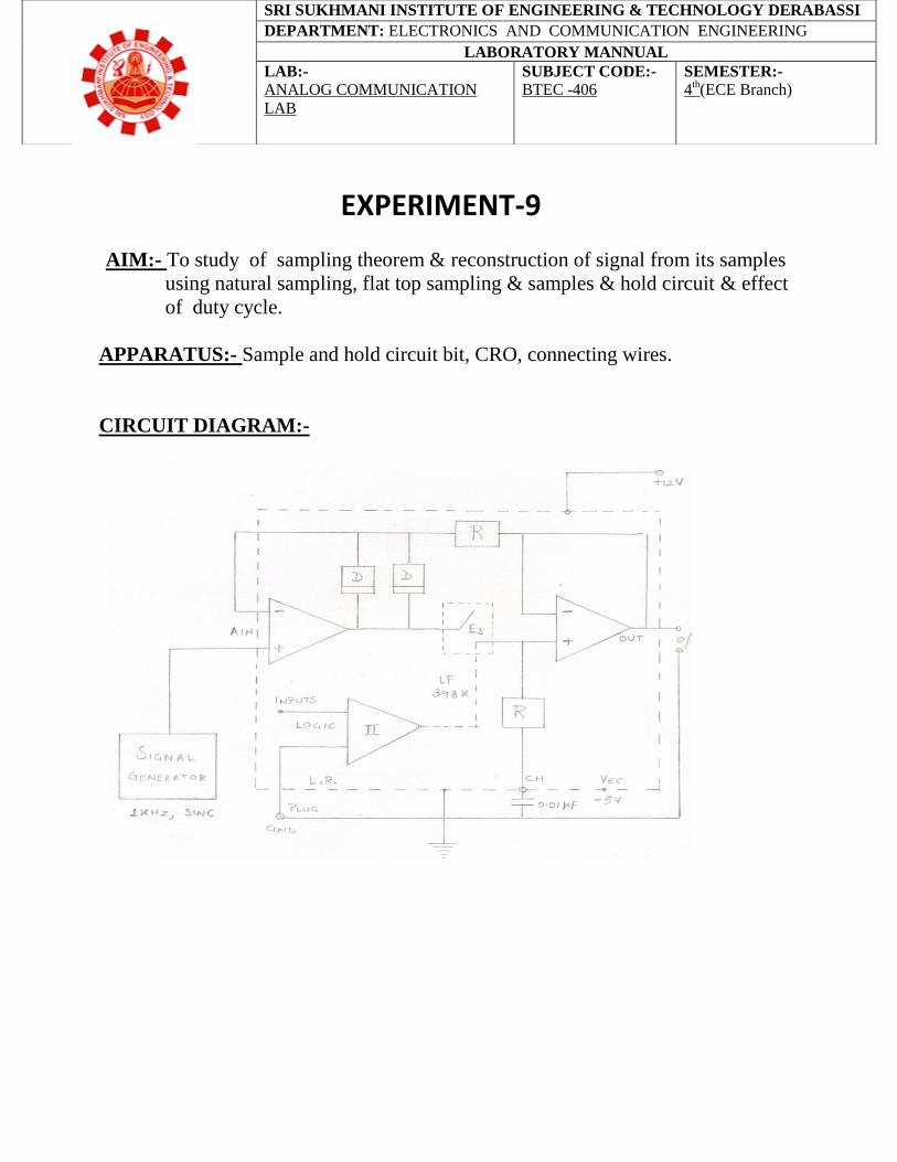
EXPERIMENT-9
AIM:- To study of sampling theorem & reconstruction of signal from its samples
using natural sampling, flat top sampling & samples & hold circuit & effect
of duty cycle.
APPARATUS:- Sample and hold circuit bit, CRO, connecting wires.
CIRCUIT DIAGRAM:-
SRI SUKHMANI INSTITUTE OF ENGINEERING & TECHNOLOGY DERABASSI
DEPARTMENT: ELECTRONICS AND COMMUNICATION ENGINEERING
LABORATORY MANNUAL
LAB:-
ANALOG COMMUNICATION
LAB
SUBJECT CODE:-
BTEC -406 SEMESTER:-
4th(ECE Branch)
THEORY:-
The sample and hold circuit is designed to study the sampling of an analog time
varying single. The loads had inbuilt sin wave single source which is synchronised
with pulse generator which generator four different frequency single. The duty
factor of pulse can be for 0.1 or 0.5 by means of miniature toggle switch. Two hold
capacitors are provided to observe drop rate on sampling times. The sampling is
done by a sample and hold amplifier chip type LM398K. The disruption of the load
control and socket are:-
1.POWER ON:- It is a miniature toggle switch meant for power ON/OFF.
2.SINGLE GENERATOR:- 1 KHZ sine wave generated by direct synthesis
which is synchronised with the pulse generator rate of facilitate to observe wave
form in steady state. In amplitude control is provided to bring its O/P amp. From
zero to maximum Level.
3.CRO TRIGGER:- Pair of socket is provided to synchronise cathode ray
oscilloscope for standby or steady waveform. The CRO should be externally
triggered while using this facility. The amplitude is 4vpp square wave.
4.PULSE GENERATOR:- The pulse generator is composed of digital circuiting
has for preselect frequency and circuit single W/C and he obtained at sample pulse
O/P socket. The spot frequencies are skeletal by sample frequency selector and the
duty factor is controlled between 0.1-0.5 by D.F. switch.
5.C(SWITCH)SELECT:- Another miniature toggle select two different value of
hold capacitor C.
6.SAMPLE AND HOLD AMPLIFIEER:-Type LM398 unit its internal work
diagram is printed upon the panel. The analog is directly connected with sample
pulse O/P in turn should be connected with sample frequencies or trigger out
socket for low frequencies sampling.
SAMPLING THEROM:- If pulse modulation system, the no. of discrete steps of
an information time signal x(t) can be completely represented in its sample from
and recovered lock from sample from if sampling frequency fs≥2fm. Where fm is
the maximum frequency of continuous signal x(t).
The sampling thermo puts limit on the minimum value of sampling frequency fs. It
is define as nyquist rate.
PROCEDURE:-
1. Take the sample and hold circuit kit.
2. Connect the CRO and connect it at CRO trigger switch.
3. Now connect the sample the sample pulse sample with I/P socket.
4. Now take O/P occur O/P terminal with help of CRO.
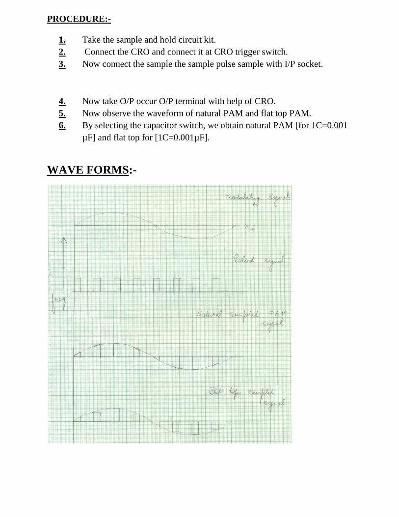
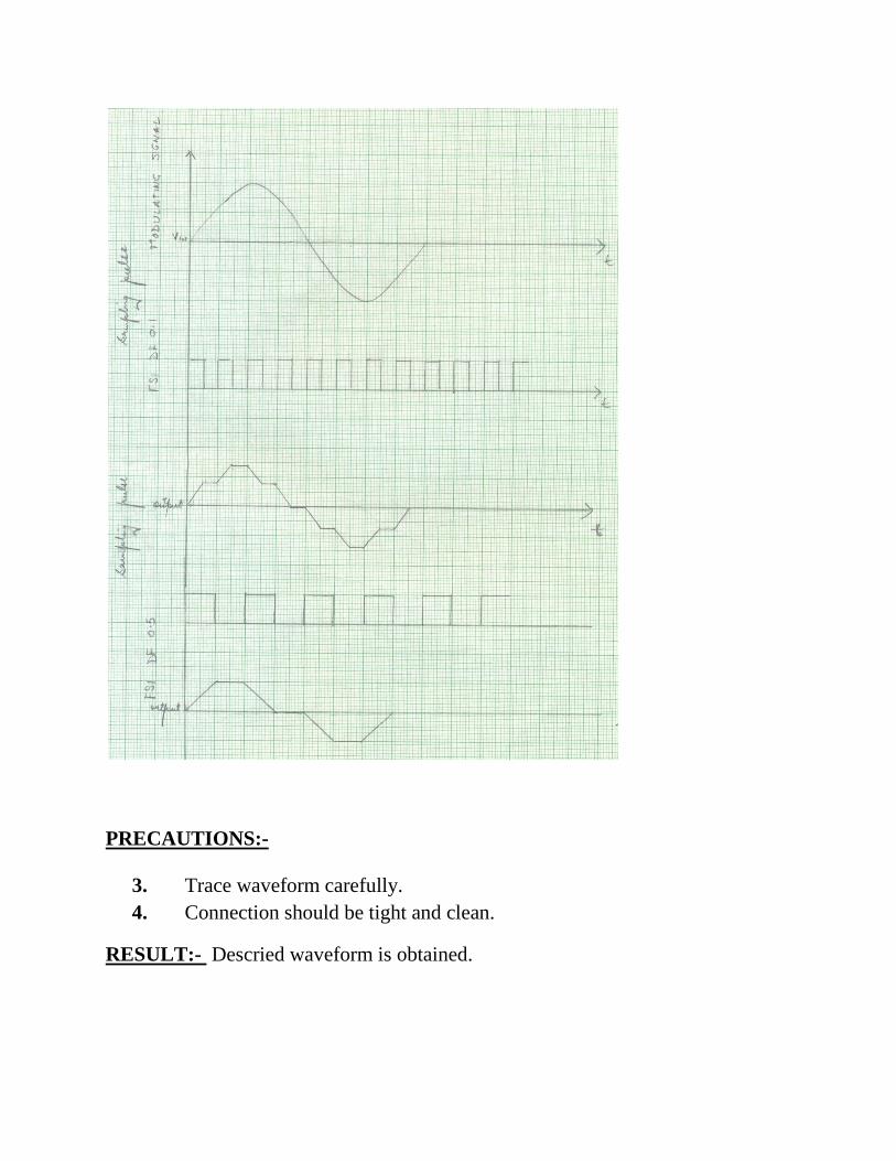
5. Now observe the waveform of natural PAM and flat top PAM.
6. By selecting the capacitor switch, we obtain natural PAM [for 1C=0.001
µF] and flat top for [1C=0.001µF].
WAVE FORMS:-
PRECAUTIONS:-
3. Trace waveform carefully.
4. Connection should be tight and clean.
RESULT:- Descried waveform is obtained.
EXPERIMENT NO-10(A)
AIM:- STUDY OF FOLDED DIPOLE ANTENNAS.
APPARATUS:-
a) Dipole antenna X 2, Folded dipole antenna.
b) ATS 10 instrument.
c) Antenna transmitter Tripod and Receiver Stepper tripod with connecting
cables, Measuring tape.
PROCEDURE:-
1. Connect the Dipole Antenna to the tripod and set the attenuator high for high
RF output. Set the length of the antenna to ƛ /2-5% or 24 cm end to end
.Keep the antenna in horizontal direction.
2. Now connect another dipole antenna to the stepper pod and set the receiver
to 600 MHz .Set the attenuator to low. Adjust the dipole for resonance at 60
MHz.
3. Set the distance between the antennas to be around 1m.Remove any stray
object from around the antennas, especially in the line of sight. Avoid any
unnecessary movement while taking the readings.
4. Now rotate the dipole antenna around its axis in steps of 5 degrees. Take the
level readings and note down.
5. Note the maximum reading out of the whole set of readings. This will form
the 0dB reference reading. Now subtract all the readings from this reference
SRI SUKHMANI INSTITUTE OF ENGINEERING & TECHNOLOGY DERABASSI
DEPARTMENT: ELECTRONICS AND COMMUNICATION ENGINEERING
LABORATORY MANNUAL
LAB:-
ANALOG COMMUNICATION
LAB
SUBJECT CODE:-
BTEC -406 SEMESTER:-
4th(ECE Branch)
readings and note down. Now use this new set of readings for drawing a
plot.
6. Plot the readings on a pole or Cartesian plane with log/linear scales on the
graph papers provided at the back of the manual.
7. This plot with both the dipoles in horizontal plane shall form an Azimuth
plot.
8. Now without disturbing the setup - rotate the dipole antenna at receiver
from horizontal to vertical plane.
9. And rotate the dipole antenna around its axis in steps of 5 degrees. Take the
level readings of receiver at each step and note down.
10. Plot the readings also on a poler or Cartesian plane with log/linear scales on
the graph papers provided at the back of the manual.
11. This plot shall constitute the Elevation plot of the dipole antenna.
12. Now repeat the procedure for a folded dipole as well.
PRECAUTIONS:-
1. Trace waveform carefully.
2. Connection should be tight and clean.
RESULT:-
sEXPERIMENT NO-10(B)
AIM:-STUDY OF GROUND PLANE WITH REFLECTOR & DIRECTOR.
APPARATUS:- a) Sipole antenna X 2.
b) ATS 10 instrument.
c) Antenna transmitter Tripod and Receiver Stepper tripod with connecting
cables, Measuring tape.
d) Directional coupler, adapter.
PROCEDURE:-
1. Connect the dipole antenna to the tripod and set the attenuator to high.
Adjust dipole for resonance at 600 MHz.
2. Now connect a yagi antenna to the stepper tripod and set the receiver
to 600 MHz. Set the attenuator to low.Set the length of the antenna
according to figure below. Keep the antenna in horizontal direction.
3. Set the distance between the antennas to be around 1m. Remove any
stray abject from around the antennas, especially in the line of sight.
Avoid any unnecessary movement while taking the reading.
4. Now rotate the yagi antenna around its axis in steps of 5 degrees. Take
the level readings of receiver at each step and note down.
5. Note the maximum reading out of the whole set of readings. This will
form the 0Db reference reading. Now use this new set of readings for
drawing a plot.
SRI SUKHMANI INSTITUTE OF ENGINEERING & TECHNOLOGY DERABASSI
DEPARTMENT: ELECTRONICS AND COMMUNICATION ENGINEERING
LABORATORY MANNUAL
LAB:-
ANALOG COMMUNICATION
LAB
SUBJECT CODE:-
BTEC -406 SEMESTER:-
4th(ECE Branch)
6. Plot the readings on a polar or Cartesian plane with log/linear scales
on the graph papers provided at the back of the manual.
7. This plot with both the dipole & Yagi in horizontal plane shall form
an Azimuth plot or azimuth pattern.
8. Now without disturbing the setup – rotate the yagi antenna at receiver
from horizontal to vertical plane. Also rotate the dipole antenna to
vertical plane at the other end.
9. Now rotate the yagi antenna around its axis iin steps of 5 degrees.
Take the level readings of receiver at each step and note down.
10. Plot the reading also on a polar or Cartesian plane with log/linear
scales on the graph papers provided at the back of the manual.
11. This plot shall constitute the Elevation plot or zenith pattern of the
Yagi antenna.
12. Repeat the procedure for a 4el/3el yagi. Observe the difference in
patterns.
PRECAUTIONS:-
1. Trace waveform carefully.
2. Connection should be tight and clean.
RESULT:-
EXPERIMENT-12
AIM:-Transmission line trainer has been designs to study the simulated L.C.R.
transmission line & to find out the value of frequency & impedance experiment
from the graph.
APPARATUS:- Transmission line trainer kit.
THEORY:-
Basic principles of transmission line:-
Transmission lines are means of conveying signals or power from one point to
another from such a broad definition, any system of wires can be consider as
forming one or more transmission line. However ,if the properties of these lines
must be taken into account, the lines might as well be arranged in some simple
,constant pattern. Thus all practical transmission lines are RRnged in some uniform
pattern, this simplifies calculations, reduces costs and increases convenience.
Types of transmission line:-
One of the simplest forms of a transmission line is the open-wire line or the twisted
pair. Since the two conductor of this type of line have same relationship with
respect to ground, it is a balanced line. But this type of line has very poor shielding
properties and has a tendency to radiate. Coaxial lines are the more popular of the
two in RF communication. A coaxial line consists of a central conductor and an
outer conductor with the outer conductor reffered to as shield normally grounded.
SRI SUKHMANI INSTITUTE OF ENGINEERING & TECHNOLOGY DERABASSI
DEPARTMENT: ELECTRONICS AND COMMUNICATION ENGINEERING
LABORATORY MANNUAL
LAB:-
ANALOG COMMUNICATION
LAB
SUBJECT CODE:-
BTEC -406 SEMESTER:-
4th(ECE Branch)
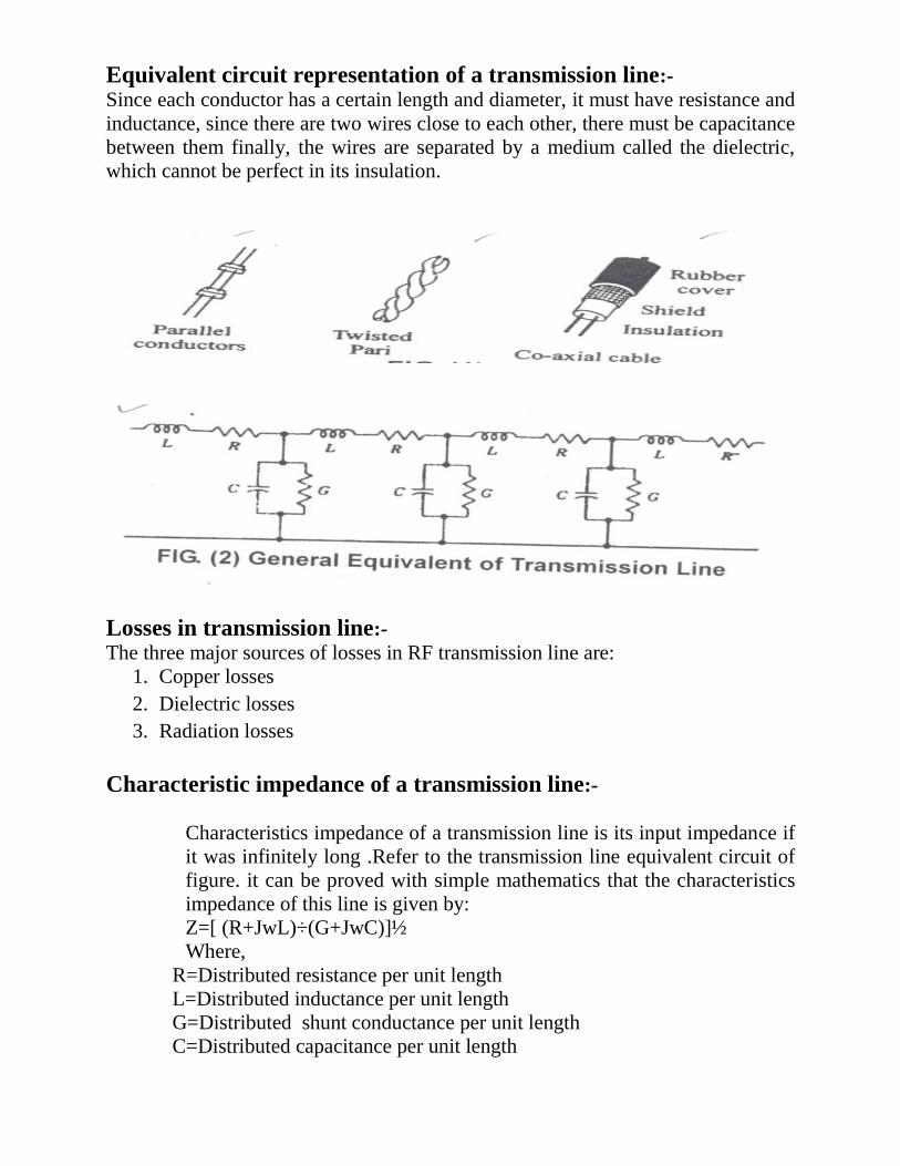
Equivalent circuit representation of a transmission line:-
Since each conductor has a certain length and diameter, it must have resistance and
inductance, since there are two wires close to each other, there must be capacitance
between them finally, the wires are separated by a medium called the dielectric,
which cannot be perfect in its insulation.
Losses in transmission line:-
The three major sources of losses in RF transmission line are:
1. Copper losses
2. Dielectric losses
3. Radiation losses
Characteristic impedance of a transmission line:-
Characteristics impedance of a transmission line is its input impedance if
it was infinitely long .Refer to the transmission line equivalent circuit of
figure. it can be proved with simple mathematics that the characteristics
impedance of this line is given by:
Z=[ (R+JwL)÷(G+JwC)]½
Where,
R=Distributed resistance per unit length
L=Distributed inductance per unit length
G=Distributed shunt conductance per unit length
C=Distributed capacitance per unit length
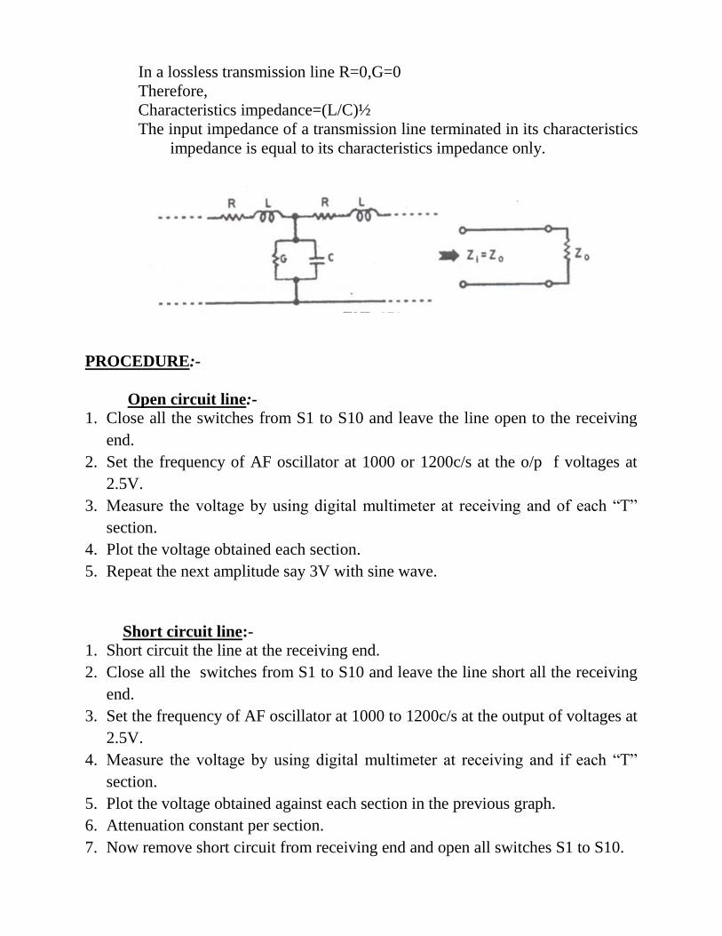
In a lossless transmission line R=0,G=0
Therefore,
Characteristics impedance=(L/C)½
The input impedance of a transmission line terminated in its characteristics
impedance is equal to its characteristics impedance only.
PROCEDURE:-
Open circuit line:-
1. Close all the switches from S1 to S10 and leave the line open to the receiving
end.
2. Set the frequency of AF oscillator at 1000 or 1200c/s at the o/p f voltages at
2.5V.
3. Measure the voltage by using digital multimeter at receiving and of each “T”
section.
4. Plot the voltage obtained each section.
5. Repeat the next amplitude say 3V with sine wave.
Short circuit line:-
1. Short circuit the line at the receiving end.
2. Close all the switches from S1 to S10 and leave the line short all the receiving
end.
3. Set the frequency of AF oscillator at 1000 to 1200c/s at the output of voltages at
2.5V.
4. Measure the voltage by using digital multimeter at receiving and if each “T”
section.
5. Plot the voltage obtained against each section in the previous graph.
6. Attenuation constant per section.
7. Now remove short circuit from receiving end and open all switches S1 to S10.
8. Keep frequency of AF oscillators at 1200c/s and output voltage at 1V.
9. First determine the voltage at the receiving end of 1st section close switch S1
and note the output voltage at the receiving end of nd section keeping input
constant, repeat for all section.
PRECAUTIONS:-
1. AF oscillator or function generator should be use in which the impedance
should be low or below to 100ohms.
2. Input audio signal should be kept constant with the prescribed amplitude,
while measuring the voltage at each “T” section.
3. Hence plot the graph by getting the readings properly.
4. Values of components are:
R=15Ohms each
C=0.01µF each
L=165µF each
5.Error in values of R,L & C components are ±2%.
RESULT:-