Embed Size (px)
Citation preview
Lab Workbook Building a Complete Embedded System
Building a Complete Embedded System Introduction This lab guides you through the process of using Vivado and IP Integrator to create a complete Zynq ARM Cortex-A9 based processor system targeting either the Zybo or ZedBoard Zynq development boards. You will use the Block Design feature of IP Integrator to configure the Zynq PS and add IP to create the hardware system, and SDK to create an application to verify the design functionality.
Objectives After completing this lab, you will be able to: • Create an embedded system design using Vivado and SDK flow • Configure the Processing System (PS) • Add Xilinx standard IP in the Programmable Logic (PL) section • Use and route the GPIO signal of the PS into the PL using EMIO • Use SDK to build a software project and verify the design functionality in hardware.
Procedure This lab is separated into steps that consist of general overview statements that provide information on the detailed instructions that follow. Follow these detailed instructions to progress through the lab.
This lab comprises eight primary steps: You will create a top-level project using Vivado, create the processor system using the IP Integrator, add two instances of the GPIO IP, validate the design, generate the bitstream, export to the SDK, create an application in the SDK, and, test the design in hardware.
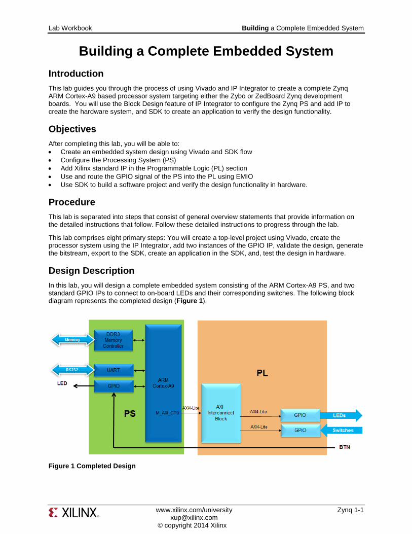
Design Description In this lab, you will design a complete embedded system consisting of the ARM Cortex-A9 PS, and two standard GPIO IPs to connect to on-board LEDs and their corresponding switches. The following block diagram represents the completed design (Figure 1).
Figure 1 Completed Design
www.xilinx.com/university Zynq 1-1 [email protected] © copyright 2014 Xilinx
Building a Complete Embedded System Lab Workbook
General Flow for this Lab
Create a Vivado Project Step 1
1-1. Launch Vivado and create an empty project targeting the Zybo or ZedBoard Zynq Evaluation and Development Kit and using the VHDL language.
1-1-1. Open Vivado by selecting Start > All Programs > Xilinx Design Tools > Vivado 2014.3.1 > Vivado 2014.3.1
1-1-2. Click Create New Project to start the wizard. You will see the Create A New Vivado Project dialog box. Click Next.
1-1-3. Click the Browse button of the Project Location field of the New Project form, browse to c:\xup\adv_embedded\labs, and click Select.
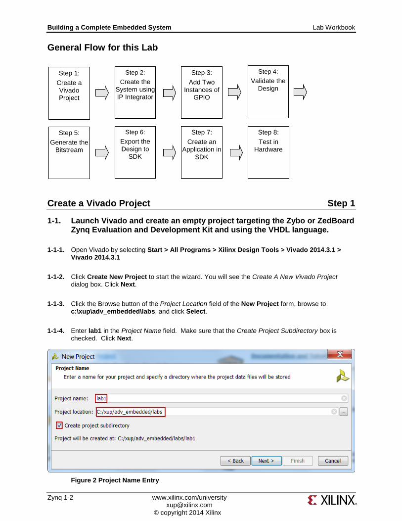
1-1-4. Enter lab1 in the Project Name field. Make sure that the Create Project Subdirectory box is checked. Click Next.
Figure 2 Project Name Entry
Step 1: Create a Vivado Project
Step 2: Create the
System using IP Integrator
Step 3: Add Two
Instances of GPIO
Step 4: Validate the
Design
Step 5: Generate the
Bitstream
Step 6: Export the Design to
SDK
Step 7: Create an
Application in SDK
Step 8: Test in
Hardware
Zynq 1-2 www.xilinx.com/university [email protected] © copyright 2014 Xilinx

Lab Workbook Building a Complete Embedded System 1-1-5. Select the RTL Project option in the Project Type form, and click Next.
1-1-6. Select VHDL as the Target Language and Simulation Language in the Add Sources form, and click Next.
1-1-7. Click Next two more times to skip adding IP or constraints.
1-1-8. In the Default Part form, using Specify Boards to filter via evaluation board type.
1-1-9. Click on the Board Vendor button.
1-1-10. Select either the Zybo or the ZedBoard Zynq Evaluation and Development Kit of the appropriate Board Version based on the board you have and click Next.
It is important to select the correct revision of the board, as the FSBL created later will generate different code depending on the board revision (i.e. silicon version) you are using. For the Zedboard the revision is likely to be “C” or “D”.
Figure 3 Board Selection
1-1-11. Click Finish to create an empty Vivado project.
www.xilinx.com/university Zynq 1-3 [email protected] © copyright 2014 Xilinx

Building a Complete Embedded System Lab Workbook
Creating the Hardware System Using IP Integrator Step 2
2-1. Create block design in the Vivado project using IP Integrator to generate the ARM Cortex-A9 processor based hardware system.
2-1-1. In the Flow Navigator, click Create Block Design under IP Integrator.
2-1-2. Name the block system and click OK.
2-1-3. Click on Add IP in the message at the top of the Diagram panel.
2-1-4. Once the IP Catalog is open, type zy into the Search bar, and double click on ZYNQ7 Processing System entry to add it to the design.
2-1-5. Click on Run Block Automation and click OK to automatically configure the board presets.
Figure 4 Zynq System Configuration View
2-1-6. Double click on the Zynq block to open the Customization window for the Zynq processing system.
A block diagram of the Zynq PS should now be open, showing various configurable blocks of the Processing System.
At this stage, designer can click on various configurable blocks (highlighted in green) and change the system configuration.
Zynq 1-4 www.xilinx.com/university [email protected] © copyright 2014 Xilinx
Lab Workbook Building a Complete Embedded System
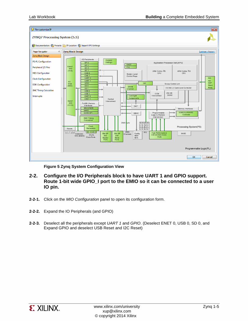
Figure 5 Zynq System Configuration View
2-2. Configure the I/O Peripherals block to have UART 1 and GPIO support. Route 1-bit wide GPIO_I port to the EMIO so it can be connected to a user IO pin.
2-2-1. Click on the MIO Configuration panel to open its configuration form.
2-2-2. Expand the IO Peripherals (and GPIO)
2-2-3. Deselect all the peripherals except UART 1 and GPIO. (Deselect ENET 0, USB 0, SD 0, and Expand GPIO and deselect USB Reset and I2C Reset)
www.xilinx.com/university Zynq 1-5 [email protected] © copyright 2014 Xilinx
Building a Complete Embedded System Lab Workbook
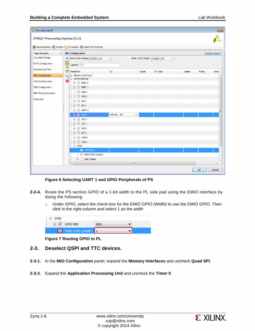
Figure 6 Selecting UART 1 and GPIO Peripherals of PS
2-2-4. Route the PS section GPIO of a 1-bit width to the PL side pad using the EMIO interface by doing the following:
o Under GPIO, select the check-box for the EMIO GPIO (Width) to use the EMIO GPIO. Then click in the right-column and select 1 as the width
Figure 7 Routing GPIO to PL
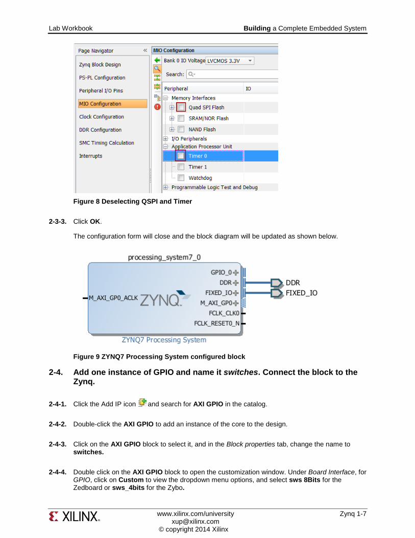
2-3. Deselect QSPI and TTC devices.
2-3-1. In the MIO Configuration panel, expand the Memory Interfaces and uncheck Quad SPI.
2-3-2. Expand the Application Processing Unit and uncheck the Timer 0.
Zynq 1-6 www.xilinx.com/university [email protected] © copyright 2014 Xilinx
Lab Workbook Building a Complete Embedded System
Figure 8 Deselecting QSPI and Timer
2-3-3. Click OK.
The configuration form will close and the block diagram will be updated as shown below.
Figure 9 ZYNQ7 Processing System configured block
2-4. Add one instance of GPIO and name it switches. Connect the block to the Zynq.
2-4-1. Click the Add IP icon and search for AXI GPIO in the catalog.
2-4-2. Double-click the AXI GPIO to add an instance of the core to the design.
2-4-3. Click on the AXI GPIO block to select it, and in the Block properties tab, change the name to switches.
2-4-4. Double click on the AXI GPIO block to open the customization window. Under Board Interface, for GPIO, click on Custom to view the dropdown menu options, and select sws 8Bits for the Zedboard or sws_4bits for the Zybo.
www.xilinx.com/university Zynq 1-7 [email protected] © copyright 2014 Xilinx
Building a Complete Embedded System Lab Workbook
As the Zybo/Zedboard was selected during the project creation, and a board support package is available for these boards, Vivado has knowledge of available resources on the board.
2-4-5. Click the IP Configuration tab. Notice the GPIO Width is set to 4 (Zybo) or 8 (Zedboard) and is greyed out. If a board support package was not available, the width of the IP could be configured here.
2-4-6. Click OK to finish configuring the GPIO and to close the Re-Customize IP window.
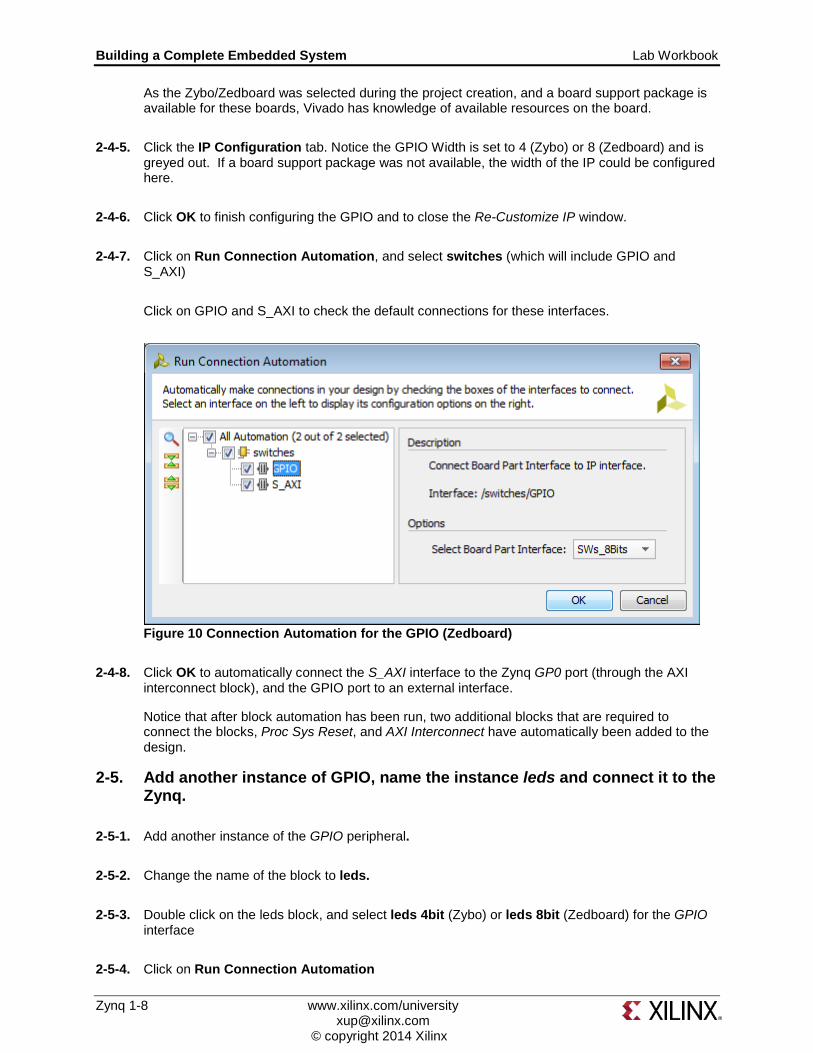
2-4-7. Click on Run Connection Automation, and select switches (which will include GPIO and S_AXI)
Click on GPIO and S_AXI to check the default connections for these interfaces.
Figure 10 Connection Automation for the GPIO (Zedboard)
2-4-8. Click OK to automatically connect the S_AXI interface to the Zynq GP0 port (through the AXI interconnect block), and the GPIO port to an external interface.
Notice that after block automation has been run, two additional blocks that are required to connect the blocks, Proc Sys Reset, and AXI Interconnect have automatically been added to the design.
2-5. Add another instance of GPIO, name the instance leds and connect it to the Zynq.
2-5-1. Add another instance of the GPIO peripheral.
2-5-2. Change the name of the block to leds.
2-5-3. Double click on the leds block, and select leds 4bit (Zybo) or leds 8bit (Zedboard) for the GPIO interface
2-5-4. Click on Run Connection Automation
Zynq 1-8 www.xilinx.com/university [email protected] © copyright 2014 Xilinx
Lab Workbook Building a Complete Embedded System 2-5-5. Click leds, and check the connections for GPIO and S_AXI as before
2-5-6. Click OK to automatically connect the interfaces as before.
Notice that the AXI Interconnect block has the second master AXI (M01_AXI) port added and connected to the S_AXI of the leds.
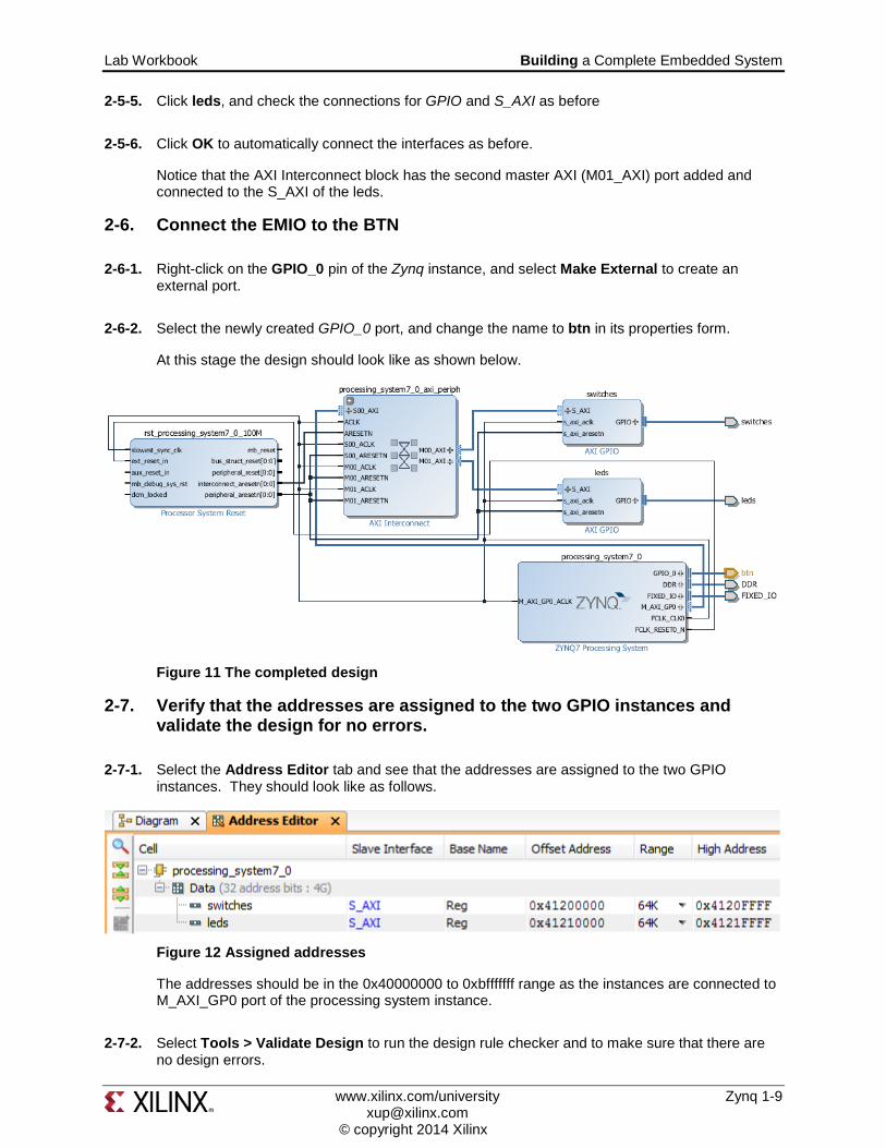
2-6. Connect the EMIO to the BTN
2-6-1. Right-click on the GPIO_0 pin of the Zynq instance, and select Make External to create an external port.
2-6-2. Select the newly created GPIO_0 port, and change the name to btn in its properties form.
At this stage the design should look like as shown below.
Figure 11 The completed design
2-7. Verify that the addresses are assigned to the two GPIO instances and validate the design for no errors.
2-7-1. Select the Address Editor tab and see that the addresses are assigned to the two GPIO instances. They should look like as follows.
Figure 12 Assigned addresses
The addresses should be in the 0x40000000 to 0xbfffffff range as the instances are connected to M_AXI_GP0 port of the processing system instance.
2-7-2. Select Tools > Validate Design to run the design rule checker and to make sure that there are no design errors.
www.xilinx.com/university Zynq 1-9 [email protected] © copyright 2014 Xilinx

Building a Complete Embedded System Lab Workbook 2-7-3. Select File > Save Block Design to save the design.
2-8. Add the provided Xilinx Design Constraints file (lab1*.xdc), which contains the BTN’s location constraint, to the project.
2-8-1. Board awareness is not being used for the EMIO button, so the pin constraints need to be provided for this interface. Click the Add Sources button in the Flow Navigator.
2-8-2. Select Add or Create Constraints, and click Next.
2-8-3. The Add or Create constraints window will appear. Click Add Files… and browse to the c:\xup\adv_embedded\sources\lab1 directory.
2-8-4. Select the lab1_zedboard.xdc or lab1_Zybo.xdc file, and click OK.
2-8-5. Click Copy constraints files into project, and click Finish to add the constraint file to the project.
Generate the Bitstream Step 3
3-1. Create the top-level HDL of the embedded system. Add the provided constraints file and generate the bitstream.
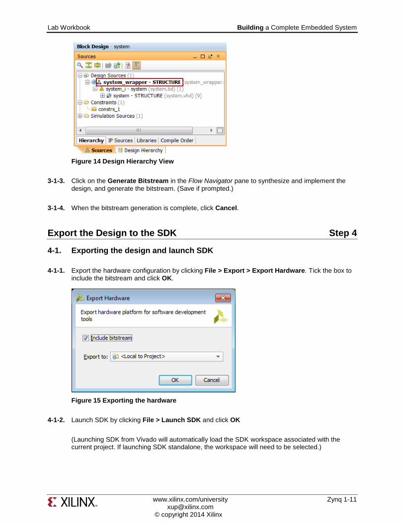
3-1-1. In Vivado, select the Sources tab, expand the Design Sources, right-click the system.bd and select Create HDL Wrapper. (Click OK when prompted to allow Vivado to automatically manage this file)
Figure 13 Selecting the system design to create the wrapper file
3-1-2. Click OK when the wrapper file, system_wrapper.vhd, is generated and added to the hierarchy. The wrapper file will be displayed in the Auxiliary pane.
Zynq 1-10 www.xilinx.com/university [email protected] © copyright 2014 Xilinx
Lab Workbook Building a Complete Embedded System
Figure 14 Design Hierarchy View
3-1-3. Click on the Generate Bitstream in the Flow Navigator pane to synthesize and implement the design, and generate the bitstream. (Save if prompted.)
3-1-4. When the bitstream generation is complete, click Cancel.
Export the Design to the SDK Step 4
4-1. Exporting the design and launch SDK
4-1-1. Export the hardware configuration by clicking File > Export > Export Hardware. Tick the box to include the bitstream and click OK.
Figure 15 Exporting the hardware
4-1-2. Launch SDK by clicking File > Launch SDK and click OK
(Launching SDK from Vivado will automatically load the SDK workspace associated with the current project. If launching SDK standalone, the workspace will need to be selected.)
www.xilinx.com/university Zynq 1-11 [email protected] © copyright 2014 Xilinx
Building a Complete Embedded System Lab Workbook
Generate an Application in SDK Step 5
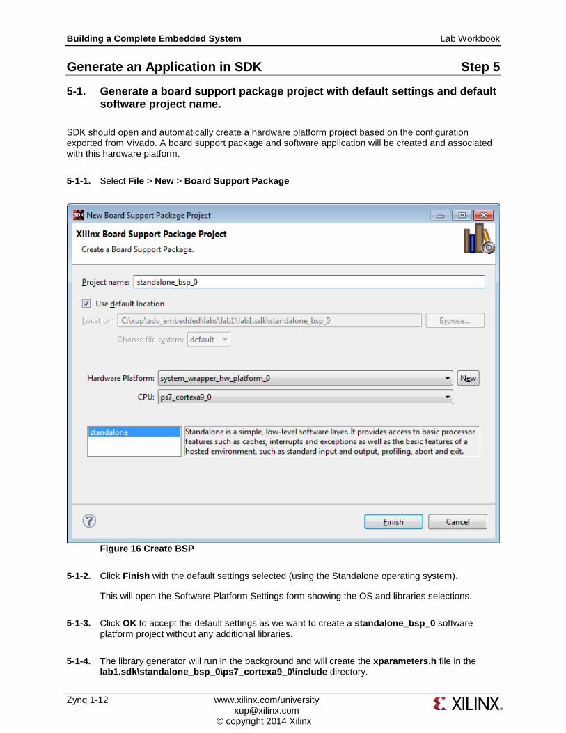
5-1. Generate a board support package project with default settings and default software project name.
SDK should open and automatically create a hardware platform project based on the configuration exported from Vivado. A board support package and software application will be created and associated with this hardware platform.
5-1-1. Select File > New > Board Support Package
Figure 16 Create BSP
5-1-2. Click Finish with the default settings selected (using the Standalone operating system).
This will open the Software Platform Settings form showing the OS and libraries selections.
5-1-3. Click OK to accept the default settings as we want to create a standalone_bsp_0 software platform project without any additional libraries.
5-1-4. The library generator will run in the background and will create the xparameters.h file in the lab1.sdk\standalone_bsp_0\ps7_cortexa9_0\include directory.
Zynq 1-12 www.xilinx.com/university [email protected] © copyright 2014 Xilinx
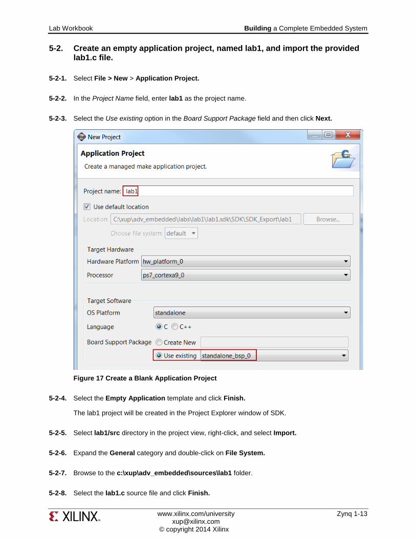
Lab Workbook Building a Complete Embedded System 5-2. Create an empty application project, named lab1, and import the provided
lab1.c file.
5-2-1. Select File > New > Application Project.
5-2-2. In the Project Name field, enter lab1 as the project name.
5-2-3. Select the Use existing option in the Board Support Package field and then click Next.
Figure 17 Create a Blank Application Project
5-2-4. Select the Empty Application template and click Finish.
The lab1 project will be created in the Project Explorer window of SDK.
5-2-5. Select lab1/src directory in the project view, right-click, and select Import.
5-2-6. Expand the General category and double-click on File System.
5-2-7. Browse to the c:\xup\adv_embedded\sources\lab1 folder.
5-2-8. Select the lab1.c source file and click Finish.
www.xilinx.com/university Zynq 1-13 [email protected] © copyright 2014 Xilinx
Building a Complete Embedded System Lab Workbook
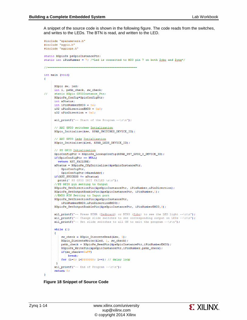
A snippet of the source code is shown in the following figure. The code reads from the switches, and writes to the LEDs. The BTN is read, and written to the LED.
Figure 18 Snippet of Source Code
Zynq 1-14 www.xilinx.com/university [email protected] © copyright 2014 Xilinx
Lab Workbook Building a Complete Embedded System
Test in Hardware Step 8
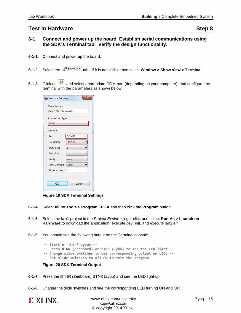
6-1. Connect and power up the board. Establish serial communications using the SDK’s Terminal tab. Verify the design functionality.
6-1-1. Connect and power up the board.
6-1-2. Select the tab. If it is not visible then select Window > Show view > Terminal.
6-1-3. Click on and select appropriate COM port (depending on your computer), and configure the terminal with the parameters as shown below.
Figure 19 SDK Terminal Settings
6-1-4. Select Xilinx Tools > Program FPGA and then click the Program button.
6-1-5. Select the lab1 project in the Project Explorer, right-click and select Run As > Launch on Hardware to download the application, execute ps7_init, and execute lab1.elf.
6-1-6. You should see the following output on the Terminal console.
Figure 20 SDK Terminal Output
6-1-7. Press the BTNR (Zedboard) BTN3 (Zybo) and see the LED light up.
6-1-8. Change the slide switches and see the corresponding LED turning ON and OFF.
www.xilinx.com/university Zynq 1-15 [email protected] © copyright 2014 Xilinx

Building a Complete Embedded System Lab Workbook 6-1-9. Set the slide switches to the ON position to exit the program.
Click the Terminate button ( ) on the Console ribbon bar to terminate the execution if you want to terminate the application at anytime before setting the slide switches to the ON position..
6-1-10. Close SDK and Vivado programs by selecting File > Exit in each program.
6-1-11. Turn OFF the power to the board.
Conclusion In this lab, you created an ARM Cortex-A9 processor based embedded system using the Zynq device for the Zybo/ZedBoard. You learned how to route the GPIO connected to the PS section to the FPGA (PL) pin using the EMIO. You instantiated the Xilinx standard GPIO IP to provide input and output functionality. You also saw that whenever the dedicated pins are not used, you need to provide pin constraints through the user constraints file (xdc).
You created the project in Vivado, created the hardware system using IPI, implemented the design in Vivado, exported the generated bitstream to the SDK, created a software application in the SDK, and verified the functionality in hardware after programming the PL section and running the application from the DDR memory.
Zynq 1-16 www.xilinx.com/university [email protected] © copyright 2014 Xilinx


![Complete Embedded Minimal Surfaces of Finite …arXiv:math/9508213v1 [math.DG] 9 Aug 1995 Complete Embedded Minimal Surfaces of Finite Total Curvature David Hoffman∗ MSRI 1000 Centennial](https://img.pdfslide.net/doc/110x75/5e3d60412c5aab7cd60ded32/complete-embedded-minimal-surfaces-of-finite-arxivmath9508213v1-mathdg-9-aug.jpg)