Embed Size (px)
Citation preview

c© 2009 Mitrabhanu Sahu
SWITCHING CURRENT DISTRIBUTIONS OF SUPERCONDUCTING NANOWIRES:EVIDENCE OF QUANTUM PHASE SLIP EVENTS
BY
MITRABHANU SAHU
B.Sc., Indian Institute of Technology, Kharagpur, 2003M.S., University of Illinois at Urbana-Champaign, 2007
DISSERTATION
Submitted in partial fulfillment of the requirementsfor the degree of Doctor of Philosophy in Physics
in the Graduate College of theUniversity of Illinois at Urbana-Champaign, 2009
Urbana, Illinois
Doctoral Committee:
Professor James Eckstein, ChairAssociate Professor Alexey Bezryadin, Director of ResearchProfessor Paul GoldbartProfessor John Stack
Abstract
Phase slips are topological fluctuation events that carry the superconducting order-parameter
field between distinct current carrying states. Owing to these phase slips low-dimensional
superconductors acquire electrical resistance. In quasi-one-dimensional nanowires it is well
known that at higher temperatures phase slips occur via the process of thermal barrier-
crossing by the order-parameter field. At low temperatures, the general expectation is that
phase slips should proceed via quantum tunneling events, which are known as quantum
phase slips (QPS). However, experimental observation of QPS is a subject of strong debate
and no consensus has been reached so far about the conditions under which QPS occurs.
In this study, strong evidence for individual quantum tunneling events undergone by the
superconducting order-parameter field in homogeneous nanowires is reported. This is ac-
complished via measurements of the distribution of switching currents–the high-bias currents
at which superconductivity gives way to resistive behavior–whose width exhibits a rather
counter-intuitive, monotonic increase with decreasing temperature. A stochastic model of
phase slip kinetics which relates the basic phase slip rates to switching rates is outlined.
Comparison with this model indicates that the phase predominantly slips via thermal ac-
tivation at high temperatures but at sufficiently low temperatures switching is caused by
individual topological tunneling events of the order-parameter field, i.e., QPS. Importantly,
measurements show that in nanowires having larger critical currents quantum fluctuations
dominate thermal fluctuations up to higher temperatures. This fact provides strong support
for the view that the anomalously high switching rates observed at low temperatures are
indeed due to QPS, and not consequences of extraneous noise or hidden inhomogeneity of
ii

the wire. In view of the QPS that they exhibit, superconducting nanowires are important
candidates for qubit implementations.
iii

To my family.
iv
Acknowledgments
The work presented in this dissertation could not have been completed without the assistance
of many people. Foremost, I would like to thank Alexey Bezryadin, my advisor, who walked
me through every step in the process of learning how to conduct experiments, analyze data,
and present results. Alexey is an excellent experimentalist and his guidance specific to my
work and in general throughout my graduate years have been extremely beneficial. I have
learned more from him than he probably knows.
I would like to thank the founding members of the Bezryadin group, Tony Bolinger,
Ulas Coskun, David Hopkins and Andrey Rogachev for their help training me in everything
from sample fabrication to data analysis. The past and present members of Alexey’s research
group have provided a continuous source of ideas, answers, and encouragement while keeping
the atmosphere in the lab very open and enjoyable. These include Thomas Aref, Rob Dins-
more, Matthew Brenner, Jaseung Ku, Mikas Remeika, Bob Colby, C. J. Lo, Anil Nandyala,
and Hisashi Kajiura. I am especially appreciative of the help and guidance I received from
Myung-Ho Bae, a postdoctoral fellow in our group, for measurements and especially for the
work on high-Tc Josephson junctions.
I would like to thank Paul Goldbart and his students, in particular David Pekker, for
their inputs and discussions. They, second to my advisor, have helped me understand the
most about the underlying physics of my experiments.
Much of the nanowire fabrication was performed in the Microfabrication and Crystal
Growth Facility and class 100 cleanroom of the Materials Research Laboratory. I thank Tony
Banks for all of his hard work in maintaining this excellent resource and for his technical
v
advice). I am also grateful to Vania Petrova and Mike Marshall of the Center for Materials
Microanalysis for instrument training and assistance.
Special thanks to Neet Priya Bajwa for her patience in proof reading my thesis and giving
very insightful comments to improve the presentation. I would like to thank Jaseung Ku
for his help in formatting the thesis in LATEX. I would like to thank my family and friends
for always believing that I would succeed. Even though I cannot name them all here, I will
always cherish their support and the time spent with them.
I would like to thank the University of Illinois Graduate College for awarding me a Disser-
tation Completion Fellowship, which allowed me to focus more on my research project. This
work was supported by the U.S. Department of Energy under Grant No. DE- FG0207ER46453.
This work was carried out in part in the Frederick Seitz Materials Research Laboratory Cen-
tral Facilities, University of Illinois, which are partially supported by the U.S. Department
of Energy under Grant Nos. DE-FG0207ER46453 and DE-FG0207ER46471.
vi
Table of Contents
List of Tables . . . . . . . . . . . . . . . . . . . . . . . . . . . . . . . . . . . . ix
List of Figures . . . . . . . . . . . . . . . . . . . . . . . . . . . . . . . . . . . . x
Chapter 1 Introduction . . . . . . . . . . . . . . . . . . . . . . . . . . . . . 1
Chapter 2 Basics of superconductivity in one dimension . . . . . . . . . . 5
2.1 Phase slip in one dimension . . . . . . . . . . . . . . . . . . . . . . . . . . . 52.2 Free energy barrier for a phase slip . . . . . . . . . . . . . . . . . . . . . . . 92.3 Little’s fit . . . . . . . . . . . . . . . . . . . . . . . . . . . . . . . . . . . . . 152.4 LAMH fit . . . . . . . . . . . . . . . . . . . . . . . . . . . . . . . . . . . . . 162.5 Comparisons with experiments . . . . . . . . . . . . . . . . . . . . . . . . . . 212.6 Quantum phase slips . . . . . . . . . . . . . . . . . . . . . . . . . . . . . . . 24
Chapter 3 Fabrication and measurements of superconducting nanowires 34
3.1 Fabrication of superconducting nanowires on top of carbon nanotubes . . . . 353.1.1 Preparation of the substrate . . . . . . . . . . . . . . . . . . . . . . . 353.1.2 Deposition of fluorinated single walled carbon nanotubes . . . . . . . 373.1.3 Sputtering of superconducting material . . . . . . . . . . . . . . . . . 393.1.4 Scanning electron microscopy . . . . . . . . . . . . . . . . . . . . . . 413.1.5 Photolithography and etching . . . . . . . . . . . . . . . . . . . . . . 43
3.2 Measurement of superconducting nanowires . . . . . . . . . . . . . . . . . . 453.2.1 Mounting the sample . . . . . . . . . . . . . . . . . . . . . . . . . . . 453.2.2 Cryostats . . . . . . . . . . . . . . . . . . . . . . . . . . . . . . . . . 463.2.3 Filtering system of 3He measurement setup . . . . . . . . . . . . . . . 483.2.4 Transport Measurements . . . . . . . . . . . . . . . . . . . . . . . . . 50
Chapter 4 Low-bias measurements of superconducting nanowires . . . . 53
4.1 Resistance vs. temperature R(T ) curves . . . . . . . . . . . . . . . . . . . . 534.2 Comparison with Little’s and LAMH fits . . . . . . . . . . . . . . . . . . . . 57
Chapter 5 Switching current measurements of superconducting nanowires 61
5.1 High-bias V (I) measurements . . . . . . . . . . . . . . . . . . . . . . . . . . 615.2 Stochasticity of switching currents . . . . . . . . . . . . . . . . . . . . . . . . 645.3 Switching current distribution measurements . . . . . . . . . . . . . . . . . . 66
vii
5.4 Standard deviation of switching current distributions . . . . . . . . . . . . . 735.5 Switching rates from switching current distributions . . . . . . . . . . . . . . 755.6 Dynamics of switching in superconducting nanowires . . . . . . . . . . . . . 805.7 Quantum phase slip and single phase-slip regime . . . . . . . . . . . . . . . . 845.8 Details of the stochastic overheating model . . . . . . . . . . . . . . . . . . . 93
5.8.1 Model for heating by phase slips . . . . . . . . . . . . . . . . . . . . . 935.8.2 Input functions and parameters . . . . . . . . . . . . . . . . . . . . . 1015.8.3 Comparison with experimental data . . . . . . . . . . . . . . . . . . . 105
Chapter 6 Multiple-retrapping process in high-Tc Josephson junctions . 116
6.1 Introduction . . . . . . . . . . . . . . . . . . . . . . . . . . . . . . . . . . . . 1166.2 Experiments . . . . . . . . . . . . . . . . . . . . . . . . . . . . . . . . . . . . 1186.3 Results and discussion . . . . . . . . . . . . . . . . . . . . . . . . . . . . . . 1206.4 Summary . . . . . . . . . . . . . . . . . . . . . . . . . . . . . . . . . . . . . 127
Appendix A MQT in high-TC intrinsic Josephson junctions . . . . . . . . 129
References . . . . . . . . . . . . . . . . . . . . . . . . . . . . . . . . . . . . . . 133
Author’s Biography . . . . . . . . . . . . . . . . . . . . . . . . . . . . . . . . . 139
viii

List of Tables
3.1 Properties of MeGe: Measured and derived physical parameters of MoGe . . 40
5.1 Nanowire sample parameters for the five measured MoGe wires. . . . . . . . 93
6.1 Fitting parameters for the switching events for selected temperatures . . . . 127
ix
List of Figures
2.1 Little’s phase slip diagram from his paper . . . . . . . . . . . . . . . . . . . 72.2 Depiction of a phase slip event . . . . . . . . . . . . . . . . . . . . . . . . . . 82.3 Gibbs free-energy barrier . . . . . . . . . . . . . . . . . . . . . . . . . . . . . 182.4 Data from Lukens et al. and Newbower et al. . . . . . . . . . . . . . . . . . 212.5 Data from Rogachev et al. and Chu et al. with TAPS fits . . . . . . . . . . . 232.6 Data from Rogachev et al. and Bollinger et al. . . . . . . . . . . . . . . . . . 242.7 Data from Giordano et al. with fits to his model of MQT . . . . . . . . . . . 252.8 Data from Lau et al. with fits to the Giordano’s model . . . . . . . . . . . . 262.9 Data from Zgirski et al. for Al wire . . . . . . . . . . . . . . . . . . . . . . . 292.10 Data from Zgirski et al. for Al wire with fit to GZ model . . . . . . . . . . . 302.11 Data from Zgirski et al. for Al wire with progressive reduction of diameter . 312.12 Data from Altomare et al. with fits to Giordano’s model . . . . . . . . . . . 33
3.1 Preparation of the substrate . . . . . . . . . . . . . . . . . . . . . . . . . . . 363.2 Deposition of Fluorinated single walled carbon nanotube . . . . . . . . . . . 383.3 Deposition of metal . . . . . . . . . . . . . . . . . . . . . . . . . . . . . . . . 413.4 Scanning Electron Microscope (SEM) images of nanowires . . . . . . . . . . 423.5 Photolithography process . . . . . . . . . . . . . . . . . . . . . . . . . . . . . 443.6 The shape of the Cr mask used in photolithography . . . . . . . . . . . . . . 453.7 Attenuation of high frequency signal in the 3He setup . . . . . . . . . . . . . 493.8 Schematic of the measurement setup for transport measurement of nanowires 51
4.1 R(T ) curve for a MoGe nanowire sample . . . . . . . . . . . . . . . . . . . . 544.2 R(T ) curves for 9 different MoGe nanowires representing SIT . . . . . . . . . 564.3 Little’s fit to the R-T data for a nanowire . . . . . . . . . . . . . . . . . . . 574.4 LAMH fit to the R-T data for a nanowire . . . . . . . . . . . . . . . . . . . 59
5.1 V (I) curves for a MoGe nanowire . . . . . . . . . . . . . . . . . . . . . . . . 625.2 V (I) curves for several temperatures illustrating the “voltage tails” . . . . . 635.3 ISW and IR measured as the sample temperature is decreased . . . . . . . . 655.4 Switching current distribution data for three different temperatures . . . . . 675.5 Switching current distributions for wire S1 . . . . . . . . . . . . . . . . . . . 685.6 Switching current distributions for wire S2 . . . . . . . . . . . . . . . . . . . 705.7 Switching current distributions for wire S3 . . . . . . . . . . . . . . . . . . . 715.8 Switching current distributions for wire S4 . . . . . . . . . . . . . . . . . . . 72
x
5.9 Switching current distributions for wire S5 . . . . . . . . . . . . . . . . . . . 735.10 Standard deviation of switching current distributions for five samples . . . . 745.11 Switching current distribution to rate conversion . . . . . . . . . . . . . . . . 765.12 Switching rates for wire S1 . . . . . . . . . . . . . . . . . . . . . . . . . . . . 775.13 Switching rates for wire S2 . . . . . . . . . . . . . . . . . . . . . . . . . . . . 785.14 Switching rates for wire S3 . . . . . . . . . . . . . . . . . . . . . . . . . . . . 785.15 Switching rates for wire S4 . . . . . . . . . . . . . . . . . . . . . . . . . . . . 795.16 Switching rates for wire S5 . . . . . . . . . . . . . . . . . . . . . . . . . . . . 795.17 Simulated “temperature bumps” in the nanowire due to phase-slips events . 815.18 Switching rates and fit to the stochastic overheating model . . . . . . . . . . 825.19 Single QPS regime . . . . . . . . . . . . . . . . . . . . . . . . . . . . . . . . 855.20 Effective quantum temperature . . . . . . . . . . . . . . . . . . . . . . . . . 875.21 Different attempt frequency for TAPS . . . . . . . . . . . . . . . . . . . . . . 895.22 Mean switching current . . . . . . . . . . . . . . . . . . . . . . . . . . . . . . 905.23 High-bias V (I) data and TAPS fit . . . . . . . . . . . . . . . . . . . . . . . . 915.24 Sketch of the overheating model . . . . . . . . . . . . . . . . . . . . . . . . . 965.25 Simulated I-V hysteresis loops . . . . . . . . . . . . . . . . . . . . . . . . . 1065.26 Comparison of switching current distributions with the overheating model . . 1085.27 Hierarchy of critical and switching currents . . . . . . . . . . . . . . . . . . . 1095.28 Comparison of standard deviation with the overheating model . . . . . . . . 1105.29 Mean switching rates and fits . . . . . . . . . . . . . . . . . . . . . . . . . . 1115.30 Single phase slip induced switch regime . . . . . . . . . . . . . . . . . . . . . 113
6.1 R vs T curve of the sample stack . . . . . . . . . . . . . . . . . . . . . . . . 1196.2 Switching current distributions and switching rates . . . . . . . . . . . . . . 1216.3 Dependence of switching current distributions on impedance . . . . . . . . . 124
A.1 Standard deviation for switching current for two samples . . . . . . . . . . . 130A.2 Switching rates obtained from the switching current distributions . . . . . . 131A.3 The escape temperature Tesc obtained at various bath temperatures . . . . . 132
xi
Chapter 1
Introduction
Quantum phenomena involving systems far larger than individual atoms are one of the most
exciting fields of modern physics. Initiated by Leggett more than twenty-five years ago,
the field of macroscopic quantum tunnelling (MQT) [1, 2, 3] has seen widespread develop-
ment. Important realizations of this being furnished, for instance, by MQT of the phase in
Josephson junctions [4, 5, 6, 7] and MQT of the magnetization in magnetic nanoparticles [8].
Martinis, Devoret and Clarke in 1987 showed that a macroscopic object can behave as a sin-
gle quantum particle [5]. They used a microwave technique and showed that a micron sized
superconducting device possesses a discrete energy spectrum in addition to showing MQT.
More recently, the breakthrough recognition of the potential advantages of quantum-based
computational methods has initiated the search for viable implementations of qubits, several
of which are rooted in MQT in superconducting systems. In particular, it has been recently
proposed by Mooij, Harmans and Nazarov that superconducting nanowires (SCNWs) could
provide a valuable setting for realizing qubits [9]. In this case, the essential behavior needed
of SCNWs is that they undergo quantum phase slip (QPS) [10] , i.e., topological quantum
fluctuations of the superconducting order-parameter field via which tunneling occurs be-
tween current-carrying states. At sufficiently low temperatures, QPS replaces the thermally
activated phase slip (TAPS) [11] dominating at higher temperatures. It has also been pro-
posed that QPS in nanowires could allow to build a current standard, and thus could play a
useful role in aspects of metrology [12]. Additionally, QPS are believed to provide the piv-
otal processes underpinning the superconductor-insulator transition observed in nanowires
[13, 14, 15, 16, 17]. Observations of QPS have been reported previously on wires having high
1
normal resistance (i.e., RN > RQ, where RQ = h/4e2 ≈ 6, 450 Ω) via low-bias resistance
(R) vs. temperature (T ) measurements [10, 18]. Yet, low-bias measurements on short wires
with normal resistance RN < RQ have been unable to reveal QPS [19, 20, 21, 14]. Also, it
has been suggested that some results ascribed to QPS could in fact have originated in in-
homogeneity of the nanowires. Thus, no consensus exists about the conditions under which
QPS occur, and qualitatively new evidence for QPS remains highly desirable.
In this study, switching current distribution measurements of superconducting Mo79Ge21
nanowires are presented [22]. This switching current is defined as the high-bias current at
which the resistance exhibits a sharp jump from a very small value to a much larger one, close
to RN . A monotonic increase in the width of the distribution as the temperature decreases
is observed. These findings are analyzed in the light of a new theoretical model [23], which
incorporates Joule-heating [24] caused by stochastically-occurring phase slips. The switching
rates yielded by the model are quantitatively consistent with the data, over the entire range
of temperatures at which measurements were performed (i.e., 0.3 K to 2.2 K for sample
S1), using both QPS and thermally-activated phase slip [11, 25, 26] (TAPS) processes. By
contrast, if only TAPSs are included, the model fails to give qualitative agreement with the
observed switching-rate behavior below 1.2 K. Thus in the SCNWs studied, the phase of
the superconducting order-parameter field slips predominantly via thermal activation at high
temperatures; however, at temperatures below 1.2 K it is quantum tunneling that dominates
the phase-slip rate. It is especially noteworthy that at even lower temperatures (i.e., below
0.7 K) both the data in the present study and the model suggest that individual phase
slips are, by themselves, capable of causing switching to the resistive state. Thus, in this
regime, one has the capability of exploring the physics of single quantum phase-slip events.
Furthermore, strong effects of QPS at high bias currents were observed even in wires with
RN < RQ. Another crucial fact is that the observed quantum behavior is more pronounced
in wires with larger critical currents. This fact allows to rule out the possibility that the
observed behavior is caused by noise or wire inhomogeneity.
2
In Chapter 2, I will discuss the physics of phase slip phenomenon and derivation of an
expression for the associated energy barrier for a phase slip event. This will be followed by
discussions on models of TAPS by Little [11] and Langer-Ambegaokar [25] and McCumber-
Halperin [26] (LAMH) and its experimental verification done by several groups. This chapter
will conclude with discussion on theoretical models for QPS and outlining experimental work
that claims observation of QPS.
In chapter 3, the method of molecular templating to fabricate the nanowires [13] used
for this study is discussed. This method employs a suspended linear molecule as a template
subjected to a thin layer of metal deposition to produce a quasi -one-dimensional system. For
this study, using fluorinated single walled nanotubes (FSWNTs) as templates, homogeneous
Mo79Ge21 superconducting nanowires are fabricated. Various setups used to perform the
measurements are also discussed. As these measurements are very sensitive to extraneous
noise, the details of the filtering system that were implemented are provided.
In chapter 4, I will discuss low-bias R(T ) measurements performed on single nanowire
samples. By low-bias measurements it is meant that the applied currents are much smaller
than the thermodynamic critical current, such that the current-voltage (V (I)) characteristics
show Ohmic behavior. It will be also shown that for the superconducting wires the resistive
transitions can be well explained by theory of TAPS. To obtain the fits, two models of
TAPS will be used, namely, Little’s fit and Langer-Ambegaokar and McCumber-Halperin
(LAMH) fit. The LAMH model is based on the assumption that the wire is homogeneous
(i.e., free from granularity). Agreement of the resistance measured in an experiment with
that predicted in LAMH model would thus indicate homogeneity of the measured wire. For
the insulating wires the R(T ) data will be shown for a few measured samples.
Switching current distributions provide a new method to overcome the difficulty in prob-
ing the superconductivity in nanowires at low temperatures associated with the small value
of the linear resistance at low temperatures. The performed switching current measurements
will be discussed in chapter 5. In these experiments, the current through the nanowire is
3
ramped up and down in time, via a triangular or sinusoidal protocol. As the current is
ramped up, the state of the wire switches from superconductive to resistive (i.e., normal),
doing so at a value of the current that is smaller than the depairing (i.e., equilibrium)
critical current; and on ramping the current down, the state gets retrapped into a supercon-
ductive state, but at a value of current smaller than the current at which switching occurred.
Hysteretic behavior such as this reflects the underlying bistability of the superconducting
nanowire. By repeatedly ramping the current up and then down, for thousand of cycles at
each temperature, thousands of values of switching and retrapping current that constitute
distributions are generated. It is found that the retrapping current is characterized by an
extremely sharp distribution, i.e., it does not vary much from run to run. In contrast, the
switching current does vary from run to run, and thus yields a distribution. These widths of
the distributions is found to increase with decrease in temperature. A stochastic overheating
model is developed to explain this behavior. The main finding of this work is that below
a crossover temperature T ∗ the fluctuations are dominated by QPS and at sufficiently low
temperatures, every single QPS causes switching in the wire.
Finally in chapter 6, measurements of switching current distribution from a phase diffu-
sion branch (PDB) to a quasiparticle tunneling branch (QTB) as a function of temperature in
a cuprate-based intrinsic Josephson junction is reported. Contrary to the thermal-activation
model, the width of the distributions increases and the corresponding switching rate shows
a nonlinear behavior with a negative curvature in a semi-logarithmic scale with decreasing
temperature, down to 1.5 K. Based on the multiple retrapping model, it is quantitatively
demonstrated that the frequency-dependent junction quality factor, representing the energy
dissipation in a phase diffusion regime, determines the observed temperature dependence of
the widths of the distributions and the switching rates. It is also shown that a retrapping
process from the QTB to the PDB is related to the low-frequency limit damping.
4
Chapter 2
Basics of superconductivity in one
dimension
One interesting property of superconductivity in quasi-one-dimensional system is the phe-
nomenon of phase slips. Phase slip processes are responsible for resistance in superconducting
nanowires. At high temperatures (but below the transition temperature TC) this resistance
is caused due to thermally activated phase slips (TAPS), in which the system makes tran-
sition across a potential barrier between two different metastable states. At sufficiently low
temperatures the general expectation is that the system would tunnel through the barrier
between two metastable states, constituting a quantum phase slip event (QPS). Until now
there are several experimental observation of TAPS which is agreement with the predictions
theoretical models. But observation of QPS remains a subject of strong debate.
In this chapter I will discuss the physics of phase-slip phenomenon and give derivation of
an expression for the associated energy barrier for a phase slip event. This will be followed by
discussions on models of TAPS and its experimental verification. This chapter will conclude
with a discussion of theoretical models for QPS and by outlining experimental work that
claims observation of QPS.
2.1 Phase slip in one dimension
According to the phenomenological model of superconductivity proposed by Ginzburg and
Landau (GL) in 1950, a spontaneous symmetry breaking occurs at the superconducting
5
transition and the superconducting state emerges, described by the complex order parameter,
ψ = ψ0eiφ (2.1)
where, ψ0 is the magnitude and φ is the phase of the order parameter. The density of
the superconducting electrons is given by, ns = |ψ|2 = ψ20, which is non-zero, below the
superconducting transition temperature TC . The GL free energy functional is
F [ψ] =
∫d3r
[α|ψ|2 +
β
2|ψ|4 +
~2
2m|∇ψ − i
e∗A
~cψ|2 +
H2
8π
](2.2)
where α strongly depends upon the temperature as, α ∝ (T − TC) (Here, A is the magnetic
vector potential). This parameter α changes sign as the temperature changes through TC ,
giving rise to superconductivity below TC . In other words, by definition TC is the highest
temperature at which |ψ|2 6= 0 gives a lower free energy than |ψ|2 = 0.
For a superconducting nanowire, in the absence of magnetic field, the supercurrent is
driven by phase gradients, with a velocity given by
vs =~
2m∇φ, (2.3)
where m is the mass of the electrons. The supercurrent through a wire of cross section A is
Is = JsA
= 2ensvsA
=e~
2mψ2
0∇φA (2.4)
Due to conservation of current we also have that |ψ0|2∇φ = constant.
The process of phase slip was first introduced by Little in 1967 [11]. This theory was
developed in order to understand the mechanism of the supercurrent decay in thin wires
6
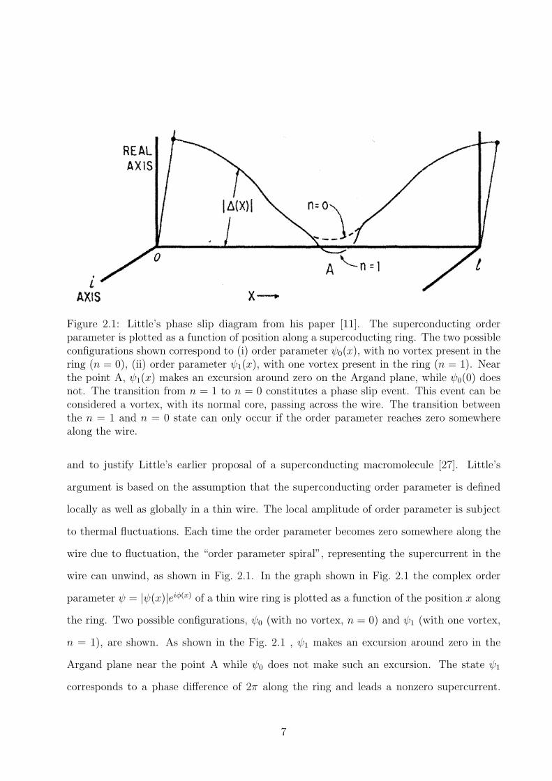
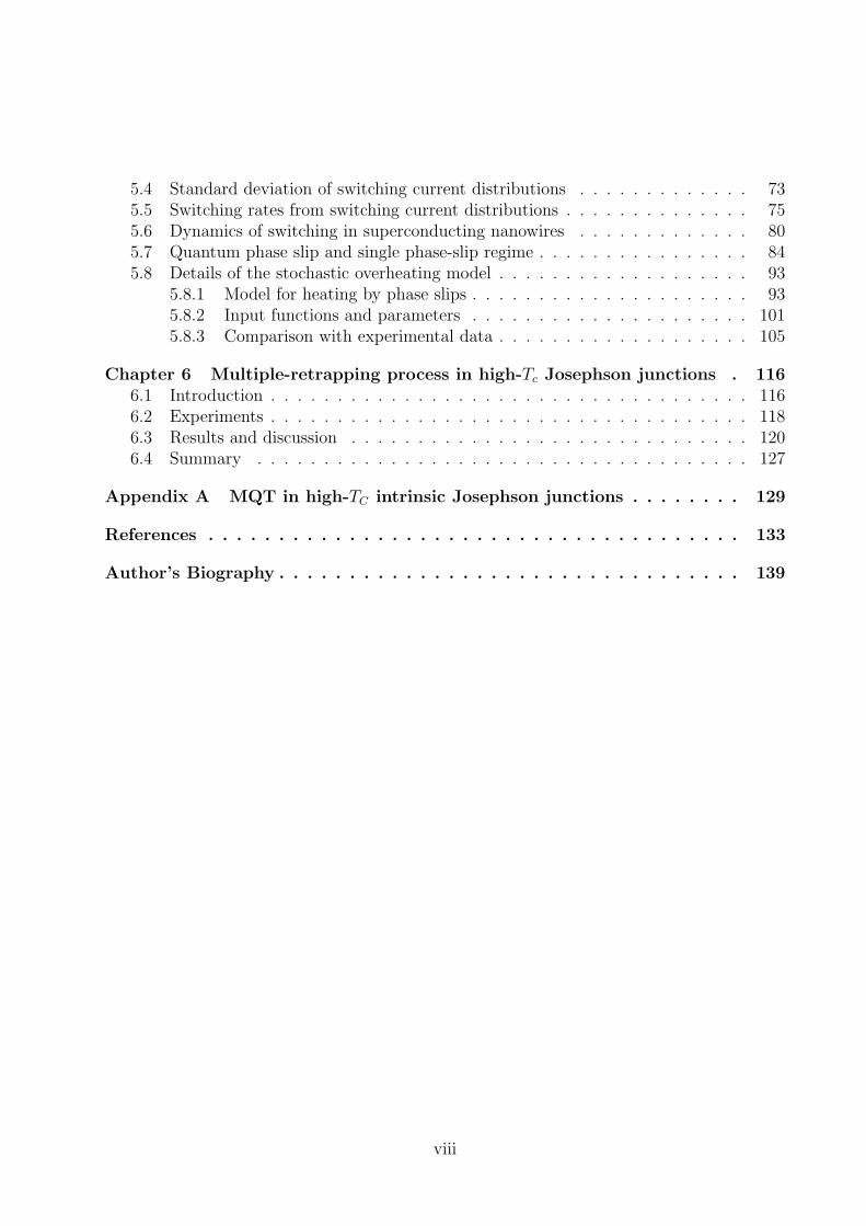
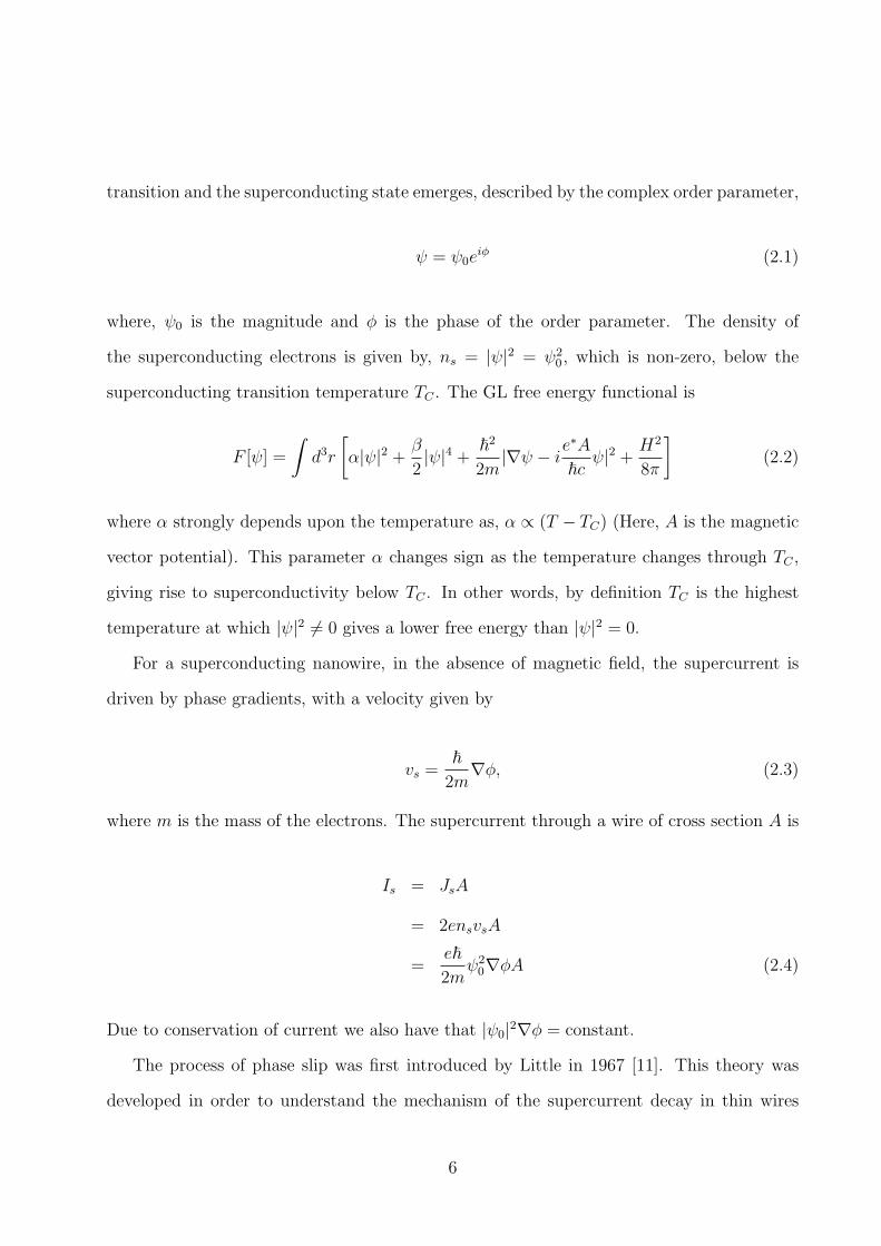
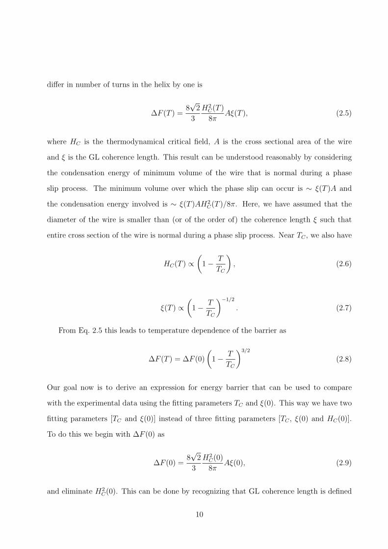
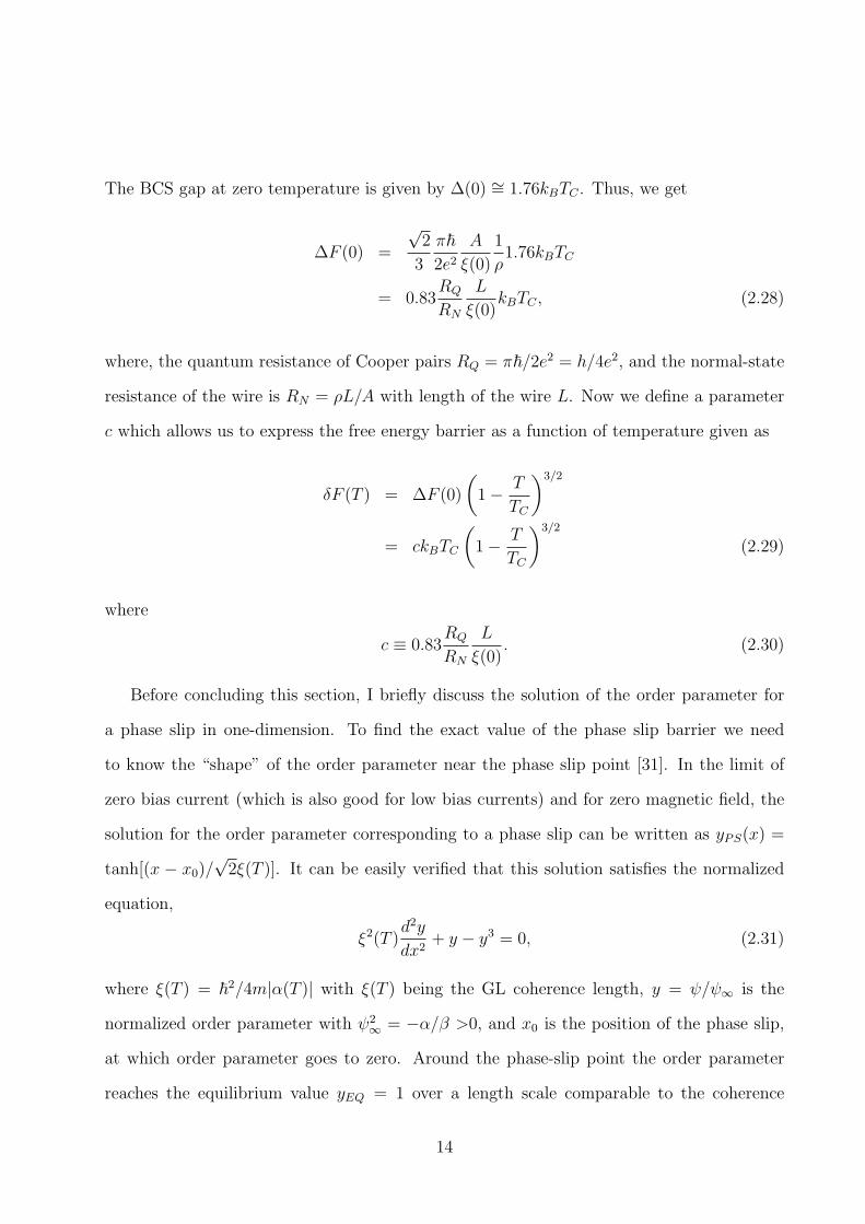
Figure 2.1: Little’s phase slip diagram from his paper [11]. The superconducting orderparameter is plotted as a function of position along a supercoducting ring. The two possibleconfigurations shown correspond to (i) order parameter ψ0(x), with no vortex present in thering (n = 0), (ii) order parameter ψ1(x), with one vortex present in the ring (n = 1). Nearthe point A, ψ1(x) makes an excursion around zero on the Argand plane, while ψ0(0) doesnot. The transition from n = 1 to n = 0 constitutes a phase slip event. This event can beconsidered a vortex, with its normal core, passing across the wire. The transition betweenthe n = 1 and n = 0 state can only occur if the order parameter reaches zero somewherealong the wire.
and to justify Little’s earlier proposal of a superconducting macromolecule [27]. Little’s
argument is based on the assumption that the superconducting order parameter is defined
locally as well as globally in a thin wire. The local amplitude of order parameter is subject
to thermal fluctuations. Each time the order parameter becomes zero somewhere along the
wire due to fluctuation, the “order parameter spiral”, representing the supercurrent in the
wire can unwind, as shown in Fig. 2.1. In the graph shown in Fig. 2.1 the complex order
parameter ψ = |ψ(x)|eiφ(x) of a thin wire ring is plotted as a function of the position x along
the ring. Two possible configurations, ψ0 (with no vortex, n = 0) and ψ1 (with one vortex,
n = 1), are shown. As shown in the Fig. 2.1 , ψ1 makes an excursion around zero in the
Argand plane near the point A while ψ0 does not make such an excursion. The state ψ1
corresponds to a phase difference of 2π along the ring and leads a nonzero supercurrent.
7
Figure 2.2: A phase slip event (a) Before the phase slip there are ten helical turns along thewire . (b) The order parameter goes to zero at some point along the wire, allowing the phaseto slip by 2π. (c) After the phase slip a helical turn has been subtracted by one. Picturetaken from Ref. [29]
The state ψ0 , on the other hand, corresponds to zero phase difference and corresponds to
zero net supercurrent. The transition from ψ1 to ψ0 constitutes a phase slip event that
topologically requires the order parameter curve to cross the x-axis. Precisely the condition
ψ = 0 needs to be satisfied at some point in time along the wire. Hence, a phase slip event
is equivalent to vortex core passing across the nanowire [28].
After each phase slip event, the phase difference between the ends of the wire can only
change by an integer multiple of 2π (see Fig. 2.2). This type of phase slippage by 2πn, unlike
phase change by any other value, does not require a voltage to be applied to the leads, since
their phases are defined by modulo 2π. The phase difference between the leads is defined
by the number of times the order parameter goes around zero on the Argand plane. As this
8
phase revolution is reduced by one loop, the phase difference is reduced by 2π.
Within Little’s model, a finite resistance occurs at constant voltage bias, according to
the following explanation. The voltage applied to the ends of the wires increases the phase
difference between the wire, and thus tends to increase the supercurrent (as Is ∝ ∇φ). Si-
multaneously, the phase slips occurring stochastically at any point along the wire tend to
decrease the supercurrent. A dynamic non-equilibrium steady state is reached at a super-
current value that is linearly dependent on the applied voltage (for small voltages). This
leads to a finite resistance. By the processes of phase slips the energy supplied at a rate IV
is dissipated as heat rather than converted into kinetic energy of the supercurrent, which
would otherwise soon exceed the condensation energy [30].
Thus, as discussed above, the process of phase slip leads to dissipation and the wire
acquires a non-zero electrical resistance. This resistance is defined by an Arrhenius type
equation with temperature dependent energy barrier. This barrier is determined by the
condensation energy required to locally suppress the order parameter to zero. The minimum
energy barrier (the ‘saddle’ point) corresponds to fluctuations in which the order parameter
is suppressed in wire segments with lengths of the order of coherence length ξ(T ). Hence
TAPS causes nanowires to remain resistive at any nonzero temperature. In the following
section the expression for the energy barrier for phase slip processes in a nanowire will be
derived.
2.2 Free energy barrier for a phase slip
The calculation of the energy barrier for phase slips was done by Langer and Ambegaokar
(LA) [25]. Using the time dependent GL theory, they found that the value of minimum free
energy barrier that separates two stationary states of a one-dimensional superconductor that
9
differ in number of turns in the helix by one is
∆F (T ) =8√
2
3
H2C(T )
8πAξ(T ), (2.5)
where HC is the thermodynamical critical field, A is the cross sectional area of the wire
and ξ is the GL coherence length. This result can be understood reasonably by considering
the condensation energy of minimum volume of the wire that is normal during a phase
slip process. The minimum volume over which the phase slip can occur is ∼ ξ(T )A and
the condensation energy involved is ∼ ξ(T )AH2C(T )/8π. Here, we have assumed that the
diameter of the wire is smaller than (or of the order of) the coherence length ξ such that
entire cross section of the wire is normal during a phase slip process. Near TC , we also have
HC(T ) ∝(
1 − T
TC
), (2.6)
ξ(T ) ∝(
1 − T
TC
)−1/2
. (2.7)
From Eq. 2.5 this leads to temperature dependence of the barrier as
∆F (T ) = ∆F (0)
(1 − T
TC
)3/2
(2.8)
Our goal now is to derive an expression for energy barrier that can be used to compare
with the experimental data using the fitting parameters TC and ξ(0). This way we have two
fitting parameters [TC and ξ(0)] instead of three fitting parameters [TC , ξ(0) and HC(0)].
To do this we begin with ∆F (0) as
∆F (0) =8√
2
3
H2C(0)
8πAξ(0), (2.9)
and eliminate H2C(0). This can be done by recognizing that GL coherence length is defined
10
by
ξ2(T ) =~
2
4m|α(T )| , (2.10)
where
α(T ) = − 2e2
mc2H2
C(T )λ2eff(T ). (2.11)
λeff is the effective penetration depth and c is the speed of light. We have for ξ(0)
ξ2(0) =~
2
4m 2e2
mc2H2
C(0)λ2eff(0)
=~
2c2
8e2H2C(0)λ2
eff(0). (2.12)
Thus we now have,
H2C(0) =
~2c2
8e2ξ2(0)λ2eff(0)
. (2.13)
Using this to eliminate HC(0) from Eq. 2.9 we get
∆F (0) =8√
2
3
H2C(0)
8πAξ(0)
=8√
2
3
1
8π
~2c2
8e2ξ2(0)λ2eff(0)
Aξ(0). (2.14)
The next step is to eliminate the effective penetration depth term in the dirty limit, which is
valid for Mo0.79Ge0.21 since 3A ≈ l ≪ λL(0) ≈ 18.5 nm (where λL is the London penetration
depth). We thus have
λ2eff(T ) = λ2
L(T )ξ0
J(0, T )l(2.15)
where ξ0 is the Pippard coherence length and l is the mean free path. Thus, we have
1
λ2eff(0)
=1
λ2L(0)
J(0, 0)l
ξ0=
1
λ2L(0)
l
ξ0(2.16)
11
where we have used for zero temperature, J(0, 0) = 1. Now we would like to eliminate the
effective penetration depth, so ∆F (0) reduces to
∆F (0) =8√
2
3
1
8π
~2c2
8e2ξ2(0)λ2eff(0)
Aξ(0)
=
√2
3
A
8π
~2c2
e2ξ(0)λ2eff(0)
=
√2
3
A
8π
~2c2
e2ξ(0)
1
λ2L(0)
l
ξ0. (2.17)
In the next step we will eliminate the London penetration depth, given by
λ2L(T ) =
mc2
4πns(T )e2, (2.18)
so we get,
1
λ2L(0)
=4πns(0)e2
mc2=
4πne2
mc2, (2.19)
where n is the density of the normal electrons. At zero temperature, almost all the electrons
are paired. Hence we are able to use n = ns(0). The free energy barrier now becomes,
∆F (0) =
√2
3
A
8π
~2c2
e2ξ(0)
1
λ2L(0)
l
ξ0
=
√2
3
A
8π
~2c2
e2ξ(0)
l
ξ0
4πne2
mc2
=
√2
3
A
2
~2
e2ξ(0)
l
ξ0
ne2
m(2.20)
From the microscopic BCS theory,
ξ0 =~vF
π∆(0), (2.21)
where vF is the Fermi velocity and ∆(0) is the superconducting gap at zero temperature, so
12
∆F (0) =
√2
3
A
2
~2
e2ξ(0)
l
ξ0
ne2
m
=
√2
3
A
2
~2
e2ξ(0)lne2
m
π∆(0)
~vF
=
√2
3
π~
2e2A
ξ(0)
ne2l
mvF
∆(0). (2.22)
From Drude theory, the force on a normal metal is modeled as
mdv
dt= eE − mv
τ(2.23)
where v is the electron velocity, E is the electric field and τ is the elastic scattering time. In
the steady state, dv/dt = 0, so we have
eE =mv
τ(2.24)
from which we get Ohm’s law,
j = nev =ne2τ
mE = σE. (2.25)
From conductivity we get the resistivity ρ:
σ =ne2τ
m=ne2l
mvF
=1
ρ, (2.26)
and using this in Eq. 2.22 we arrive at
∆F (0) =
√2
3
π~
2e2A
ξ(0)
ne2l
mvF
∆(0)
=
√2
3
π~
2e2A
ξ(0)
1
ρ∆(0). (2.27)
13
The BCS gap at zero temperature is given by ∆(0) ∼= 1.76kBTC . Thus, we get
∆F (0) =
√2
3
π~
2e2A
ξ(0)
1
ρ1.76kBTC
= 0.83RQ
RN
L
ξ(0)kBTC , (2.28)
where, the quantum resistance of Cooper pairs RQ = π~/2e2 = h/4e2, and the normal-state
resistance of the wire is RN = ρL/A with length of the wire L. Now we define a parameter
c which allows us to express the free energy barrier as a function of temperature given as
δF (T ) = ∆F (0)
(1 − T
TC
)3/2
= ckBTC
(1 − T
TC
)3/2
(2.29)
where
c ≡ 0.83RQ
RN
L
ξ(0). (2.30)
Before concluding this section, I briefly discuss the solution of the order parameter for
a phase slip in one-dimension. To find the exact value of the phase slip barrier we need
to know the “shape” of the order parameter near the phase slip point [31]. In the limit of
zero bias current (which is also good for low bias currents) and for zero magnetic field, the
solution for the order parameter corresponding to a phase slip can be written as yPS(x) =
tanh[(x − x0)/√
2ξ(T )]. It can be easily verified that this solution satisfies the normalized
equation,
ξ2(T )d2y
dx2+ y − y3 = 0, (2.31)
where ξ(T ) = ~2/4m|α(T )| with ξ(T ) being the GL coherence length, y = ψ/ψ∞ is the
normalized order parameter with ψ2∞
= −α/β >0, and x0 is the position of the phase slip,
at which order parameter goes to zero. Around the phase-slip point the order parameter
reaches the equilibrium value yEQ = 1 over a length scale comparable to the coherence
14
length ξ(T ). From these solutions one can compute the barrier for a phase slip ∆F (T ), by
computing the difference between the GL free energy corresponding to yPS(x) and yEQ = 1.
Thus, one can write,
∆F (T ) = F [yPS(x)] − F [yEQ] (2.32)
where F is the functional describing the GL free energy as in Eq. 2.2. Thus, it is possible to
find the barrier for a phase slip simply by comparing exact static solutions of GL equation
(one homogeneous and one going to zero at the position of phase slip) without referring to
any equation describing the dynamics of the condensate.
2.3 Little’s fit
According to Little’s fit, the resistance of a nanowire is given as,
RLittle(T ) = RN exp
(−∆F (T )
kBT
)(2.33)
which is based on the Arrhenius rate law. Here, RN is the normal-state resistance of the wire,
kB is the Boltzmann’s constant, T is the temperature, and ∆F (T ) is the barrier for phase
slip, which is a function of temperature derived in the previous section. At temperatures
close to TC this expression is not accurate, as it gives R(TC) = RN , whereas the actual
wire resistance should be less than RN , due to superconducting fluctuations [28]. Based on
Little’s hypothesis [11], we assume that each segment of the wire can only exist in one of
the two distinct states: superconducting, i.e., the zero resistance state that occurs between
phase slip events, and the normal state that is realized during each phase slip event in
the considered segment. The resistance of the segment in this case equals its normal state
resistance. To justify Eq. 2.33 we assume that the phase-fluctuation attempt frequency Ω0
and the relaxation time of the order parameter τ are defined by the same energy scale and
are related to each other by the relation Ω0 ≈ 1/τ . The number of phase slips occurring per
15
second, according to the Arrhenius law, is ΩPS = Ω0 exp(−∆F/kBT ). The time-fraction f
during which each segment of the wire remains in the normal state is the product of the
duration τ and the number of times the order parameter reaches zero per second, which is
ΩPS. Thus we get f = τΩ0 exp(−∆F/kBT ) ≈ exp(−∆F/kBT ). In this approximate model,
during each unit of time, the wire stays normal during a time f and superconducting during
a time (1−f). Since the fluctuations are very rapid, only the average value of the resistance
can be detected. Now let us define a set of independent equivalent segments in the wire, each
having length ξ(T ) and the normal state resistance R1N = RNξ(T )/L, where L is the total
length of the wire. The time-averaged resistance of each segment is R1 ≈ R1Nf +R0(1− f),
where R0 ≡ 0 represents the resistance of each segment in the superconducting state. Finally,
the total resistance of the wire can now be written as a product of the average resistance
of each independent segment R1 and the total number of such segments L/ξ(T ). So we get
Eq. 2.33 as
RLittle(T ) =
(L
ξ(T )R1
)
=
(L
ξ(T )
)(R1Nf +R0(1 − f))
=
(L
ξ(T )
)(R1Nf)
= RN exp(−∆F (T )/kBT ) (2.34)
2.4 LAMH fit
In the LAMH theory the normal-state resistance of the wire is not explicitly included, in
contrast with Little’s fit. In the LAMH model, the effective resistance is calculated by
considering the time-evolution of the superconducting phase φ(t). To derive the LAMH
resistance using the thermally activated phase slip (TAPS) model, we first include the effect
of the bias current (IS > 0) in the wire. This makes the free energy landscape “tilted”,
16
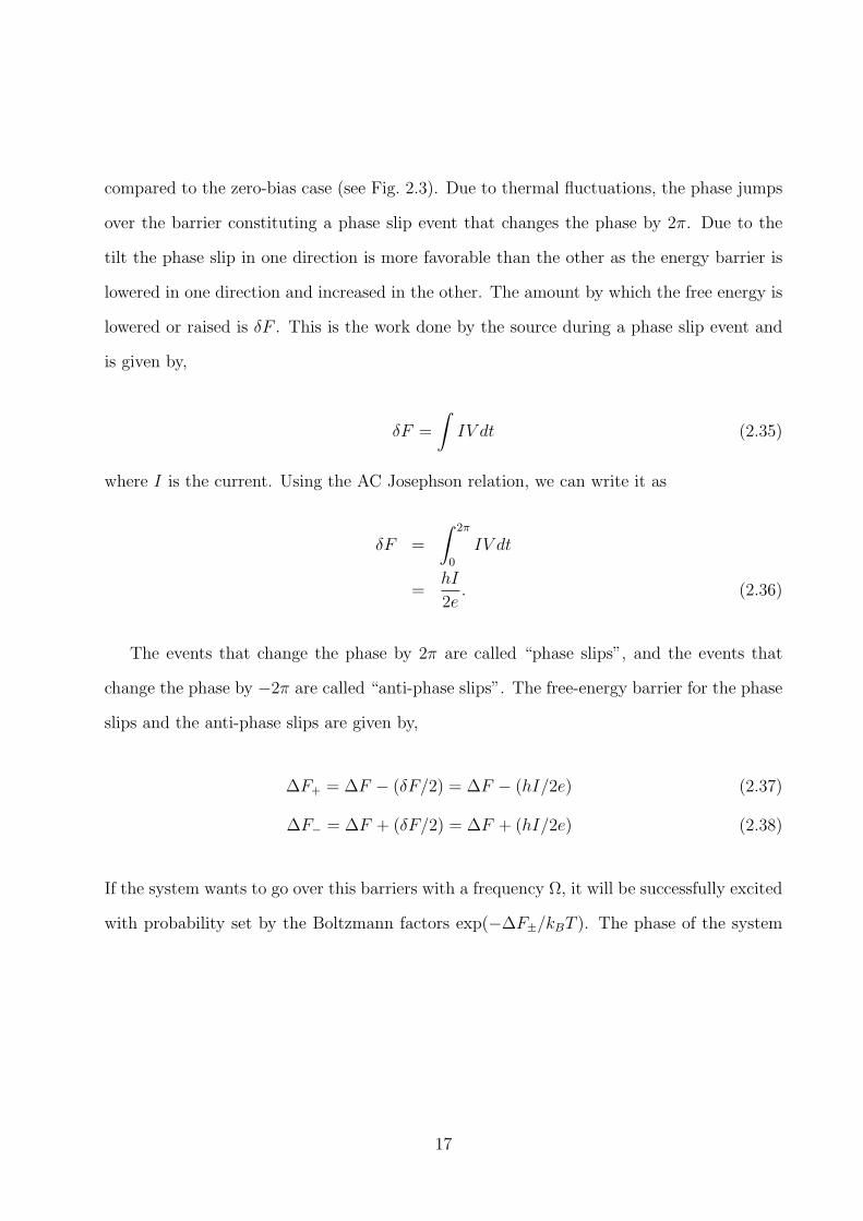
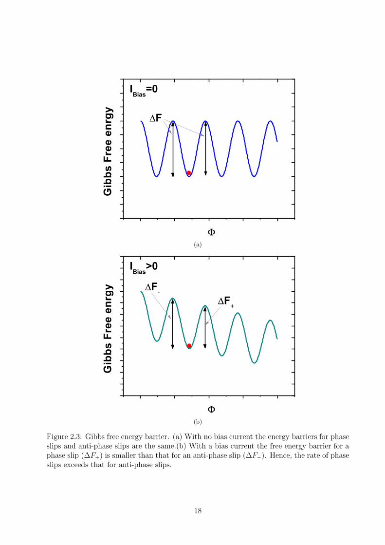
compared to the zero-bias case (see Fig. 2.3). Due to thermal fluctuations, the phase jumps
over the barrier constituting a phase slip event that changes the phase by 2π. Due to the
tilt the phase slip in one direction is more favorable than the other as the energy barrier is
lowered in one direction and increased in the other. The amount by which the free energy is
lowered or raised is δF . This is the work done by the source during a phase slip event and
is given by,
δF =
∫IV dt (2.35)
where I is the current. Using the AC Josephson relation, we can write it as
δF =
∫ 2π
0
IV dt
=hI
2e. (2.36)
The events that change the phase by 2π are called “phase slips”, and the events that
change the phase by −2π are called “anti-phase slips”. The free-energy barrier for the phase
slips and the anti-phase slips are given by,
∆F+ = ∆F − (δF/2) = ∆F − (hI/2e) (2.37)
∆F− = ∆F + (δF/2) = ∆F + (hI/2e) (2.38)
If the system wants to go over this barriers with a frequency Ω, it will be successfully excited
with probability set by the Boltzmann factors exp(−∆F±/kBT ). The phase of the system
17
Gib
bs F
ree
enrg
yF
IBias=0
(a)
Gib
bs F
ree
enrg
y F-
IBias>0
F+
(b)
Figure 2.3: Gibbs free energy barrier. (a) With no bias current the energy barriers for phaseslips and anti-phase slips are the same.(b) With a bias current the free energy barrier for aphase slip (∆F+) is smaller than that for an anti-phase slip (∆F−). Hence, the rate of phaseslips exceeds that for anti-phase slips.
18
will then be lost at a rate
dφ
dt= Ω+ − Ω−
= Ω exp(−∆F+/kBT ) − Ω exp(−∆F−/kBT )
= Ω
[exp
(∆F − hI/4e
kBT
)− exp
(∆F + hI/4e
kBT
)]
= Ωe−∆F/kBT
[exp
(hI/4e
kBT
)− exp
(−hI/4ekBT
)]
= 2Ωe−∆F/kBT sinh
(hI
4ekBT
). (2.39)
Now, the resistance can be derived from this by using the Josephson relation:
dφ
dt=
2eV
~= 2Ωe−∆F/kBT sinh
(hI
4ekBT
)
V =~Ω
ee−∆F/kBT sinh
(hI
4ekBT
). (2.40)
Differentiating the expression for voltage we get the resistance as
dV
dI=
d
dI
[~Ω
ee−∆F/kBT sinh
(hI
4ekBT
)]
=h
4e2~Ω
kBTe−∆F/kBT cosh
(hI
4ekBT
)(2.41)
When I ≪ 4ekBT/h (recall that 4ekB/h ∼= 13.4 nA/K), the hyperbolic cosine is essentially
equal to one, and the zero-bias resistance can then be given as
R = RQ~Ω
kBTe−∆F/kBT , (2.42)
where RQ = h/(2e)2 = h/4e2 is the quantum resistance for Cooper pairs.
Now we would like to discuss about the attempt frequency Ω for the phase slips. When
19
Langer and Ambegaokar formulated the theory for phase slips, they assumed for the attempt
frequency the inverse of the elastic scattering time, multiplied by the number of electrons in
the wire, i.e., nAL/τ . Later, McCumber and Halperin [26] revisited the problem, and using
time dependent GL theory they found the temperature-dependent attempt frequency
Ω =L
ξ
(∆F
kBT
)1/21
τs, (2.43)
where 1/τs = 8kB(TC − T )/π~ is the GL relaxation time which characterizes the relaxation
rate of the superconductor in the time dependent GL theory. In Eq. 2.43 1/τs sets the scale
for Ω, L/ξ is the number of independent wire segments phase slip can attempt to occur,
and√
∆F/kBT accounts for the overlap of these segments. The full dependence of the
Langer-Ambegaokar-McCumber-Halperin (LAMH) resistance can now be written as
RLAMH(T ) = Dt−3/2(1 − t)9/4 exp[c(1 − t)3/2/t] (2.44)
where we have used the notation
t = T/TC (2.45)
c = 0.83(RQ/RN)(L/ξ(0)) (2.46)
D = (8/π)(L/ξ(0))RQ
√c (2.47)
The normal quasiparticles present in the wire at T ∼ TC provide a parallel conduction
channel. Thus the net resistance can be approximated as
R−1 = R−1LAMH +R−1
N (2.48)
20
2.5 Comparisons with experiments
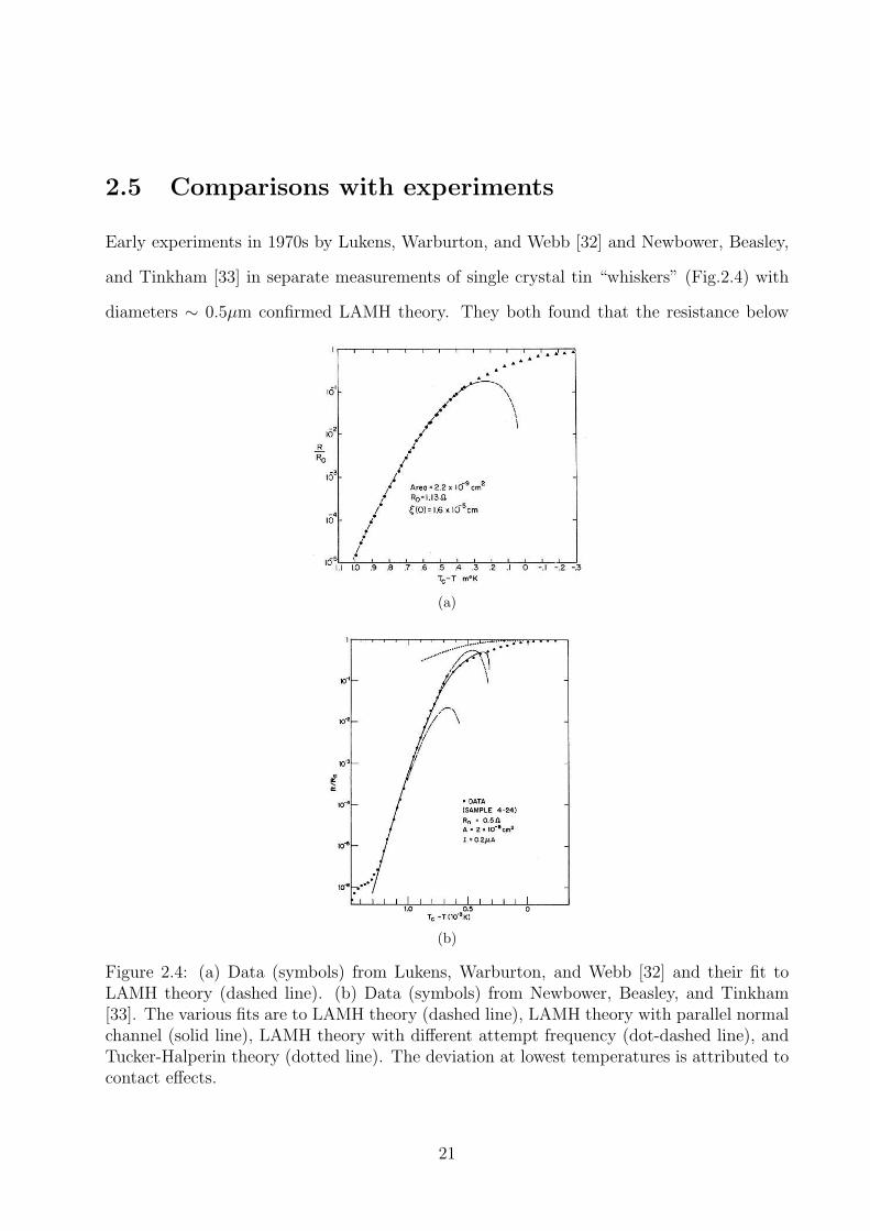
Early experiments in 1970s by Lukens, Warburton, and Webb [32] and Newbower, Beasley,
and Tinkham [33] in separate measurements of single crystal tin “whiskers” (Fig.2.4) with
diameters ∼ 0.5µm confirmed LAMH theory. They both found that the resistance below
(a)
(b)
Figure 2.4: (a) Data (symbols) from Lukens, Warburton, and Webb [32] and their fit toLAMH theory (dashed line). (b) Data (symbols) from Newbower, Beasley, and Tinkham[33]. The various fits are to LAMH theory (dashed line), LAMH theory with parallel normalchannel (solid line), LAMH theory with different attempt frequency (dot-dashed line), andTucker-Halperin theory (dotted line). The deviation at lowest temperatures is attributed tocontact effects.
21
T of the wire is well described by the LAMH theory. However, both reports do show some
deviation from the theory as T → TC but this is to be expected, as the theory is only
valid when ∆F ≫ kBT whereas as T → TC , ∆F → 0 . While the agreement between
the LAMH theory and the data of Newbower, Beasley, and Tinkham is good, they further
found that they could improve their fits by including a parallel normal channel such that
R−1 = R−1LAMH +R−1
N .
It has now been established by several experiments on ultra thin MoGe and Nb nanowires
that LAMH and Little’s fits explain the resistive transitions in homogeneous nanowires.
Rogachev et al. [21] have shown that in the absence as well as presence of magnetic field
the resistance of the nanowire follows the predictions of the LAMH theory up to 11 orders
of magnitude (in the range of 103 − 10−8Ω). The data and the fit to the LAMH theory are
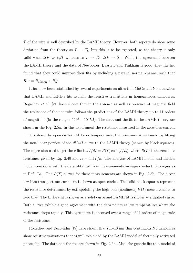
shown in the Fig. 2.5a. In this experiment the resistance measured in the zero-bias-current
limit is shown by open circles. At lower temperatures, the resistance is measured by fitting
the non-linear portion of the dV/dI curve to the LAMH theory (shown by black squares).
The expression used to get these fits is dV/dI = R(T ) cosh(I/I0), where R(T ) is the zero-bias
resistance given by Eq. 2.40 and I0 = 4ekT/h. The analysis of LAMH model and Little’s
model were done with the data obtained from measurements on superconducting bridges as
in Ref. [34]. The R(T ) curves for these measurements are shown in Fig. 2.5b. The direct
low bias transport measurement is shown as open circles. The solid black squares represent
the resistance determined by extrapolating the high bias (nonlinear) V (I) measurements to
zero bias. The Little’s fit is shown as a solid curve and LAMH fit is shown as a dashed curve.
Both curves exhibit a good agreement with the data points at low temperatures where the
resistance drops rapidly. This agreement is observed over a range of 11 orders of magnitude
of the resistance.
Rogachev and Bezryadin [19] have shown that sub-10 nm thin continuous Nb nanowires
show resistive transitions that is well explained by the LAMH model of thermally activated
phase slip. The data and the fits are shown in Fig. 2.6a. Also, the generic fits to a model of
22
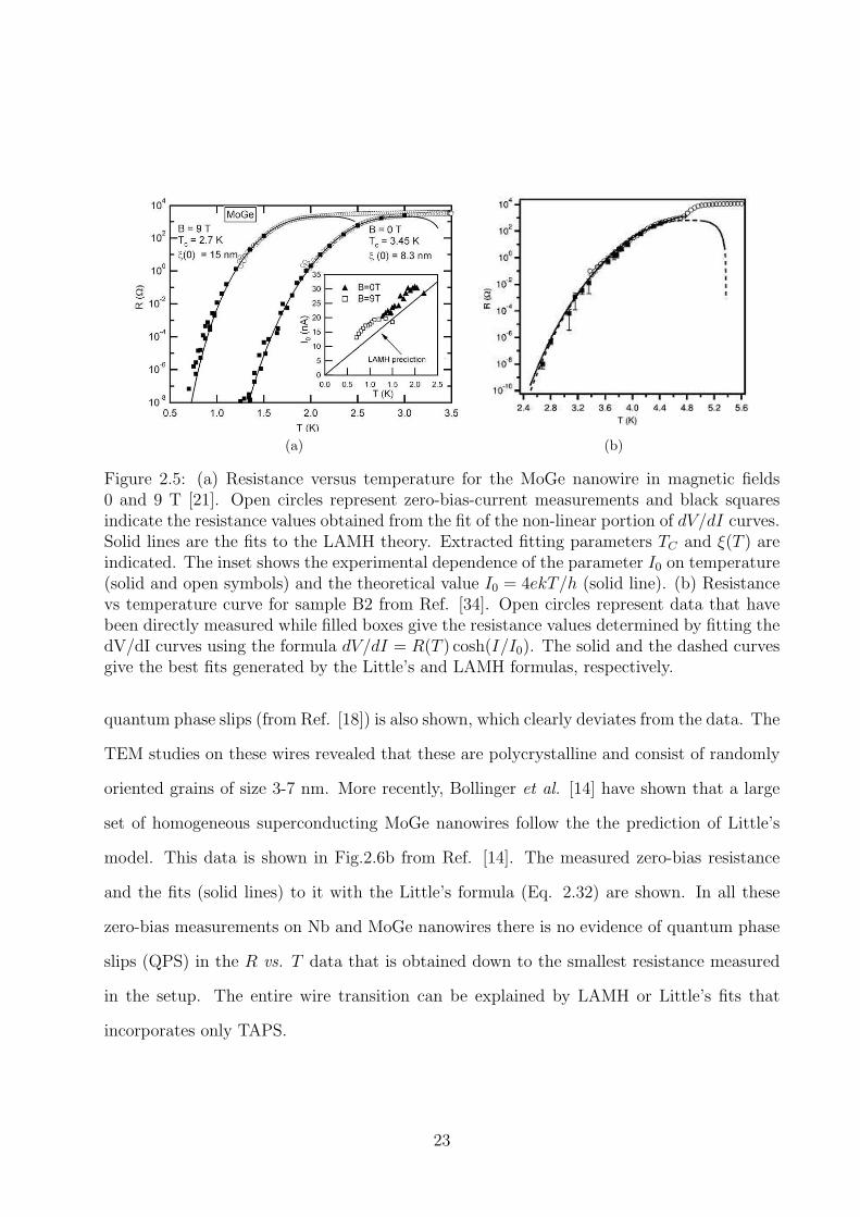
(a) (b)
Figure 2.5: (a) Resistance versus temperature for the MoGe nanowire in magnetic fields0 and 9 T [21]. Open circles represent zero-bias-current measurements and black squaresindicate the resistance values obtained from the fit of the non-linear portion of dV/dI curves.Solid lines are the fits to the LAMH theory. Extracted fitting parameters TC and ξ(T ) areindicated. The inset shows the experimental dependence of the parameter I0 on temperature(solid and open symbols) and the theoretical value I0 = 4ekT/h (solid line). (b) Resistancevs temperature curve for sample B2 from Ref. [34]. Open circles represent data that havebeen directly measured while filled boxes give the resistance values determined by fitting thedV/dI curves using the formula dV/dI = R(T ) cosh(I/I0). The solid and the dashed curvesgive the best fits generated by the Little’s and LAMH formulas, respectively.
quantum phase slips (from Ref. [18]) is also shown, which clearly deviates from the data. The
TEM studies on these wires revealed that these are polycrystalline and consist of randomly
oriented grains of size 3-7 nm. More recently, Bollinger et al. [14] have shown that a large
set of homogeneous superconducting MoGe nanowires follow the the prediction of Little’s
model. This data is shown in Fig.2.6b from Ref. [14]. The measured zero-bias resistance
and the fits (solid lines) to it with the Little’s formula (Eq. 2.32) are shown. In all these
zero-bias measurements on Nb and MoGe nanowires there is no evidence of quantum phase
slips (QPS) in the R vs. T data that is obtained down to the smallest resistance measured
in the setup. The entire wire transition can be explained by LAMH or Little’s fits that
incorporates only TAPS.
23
(a) (b)
Figure 2.6: (a) Temperature dependence of the resistance of superconducting Nb nanowires(from Ref. [19]). Solid lines show the fits to the LAMH theory. The samples Nb1, Nb2,Nb3, Nb5, and Nb6 have the following fitting parameters. Transition temperatures in Kare TC = 5.8, 5.6, 2.7, 2.5, and 1.9 , respectively. Coherence lengths in nm are ξ(0)=8.5,8.1, 18, 16, and 16.5, respectively. The dashed lines are theoretical curves that include thecontribution of quantum phase slips into the wire resistance [18], with generic factors a = 1and B = 1. The dotted lines are computed with a = 1.3 and B = 7.2. (b) R vs T data forsuperconducting wires and the fits (solid lines) to the Little formula (from Ref. [14]).
2.6 Quantum phase slips
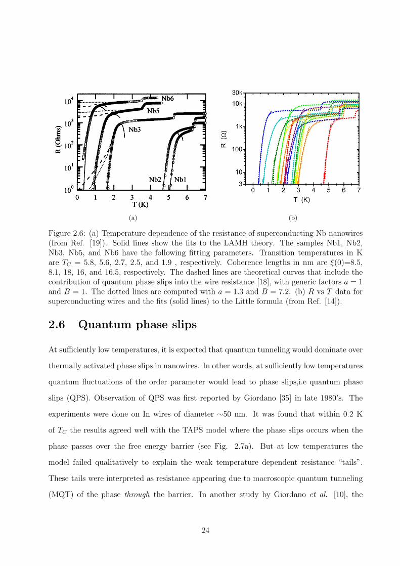
At sufficiently low temperatures, it is expected that quantum tunneling would dominate over
thermally activated phase slips in nanowires. In other words, at sufficiently low temperatures
quantum fluctuations of the order parameter would lead to phase slips,i.e quantum phase
slips (QPS). Observation of QPS was first reported by Giordano [35] in late 1980’s. The
experiments were done on In wires of diameter ∼50 nm. It was found that within 0.2 K
of TC the results agreed well with the TAPS model where the phase slips occurs when the
phase passes over the free energy barrier (see Fig. 2.7a). But at low temperatures the
model failed qualitatively to explain the weak temperature dependent resistance “tails”.
These tails were interpreted as resistance appearing due to macroscopic quantum tunneling
(MQT) of the phase through the barrier. In another study by Giordano et al. [10], the
24
superconducting state of PbIn wires were studied. The smallest samples which had diameters
below 200A showed significant dissipation below TC (see Fig. 2.7b). They also found that
the voltage-current characteristics showed oscillatory behavior which were more pronounced
as the temperature decreased. They proposed that the observed behavior is due to quantum
tunneling of the order parameter and due to existence of discrete energy levels.
(a) (b)
Figure 2.7: (a) Resistance normalized by their normal state resistance as a function oftemperature for three In wires from Ref. [35].The sample diameters were 410 A (•), 505 A(+), 720 A (). The solid lines are fits according to the thermal activation model and dashedlines are the fits to a QPS model (to be discussed later). When the solid and dashed curvesoverlap only the former is shown for clarity. The wire lengths were 80, 150, 150 µm and thenormal-state resistance were 5.7, 7.1, 1.2 kΩ respectively. (b) Resistance as a function oftemperature for several PbIn samples from [10]. The sample diameters are indicated in thefigure.
Giordano proposed a heuristic argument that the resistance from MQT follows a form
similar to that of LAMH model (Eqn. 2.42), except that the appropriate energy scale is
~/τGL instead of kBT [10, 18]. Hence the expression for the resistance due to QPS is given
by,
RQPS = Bπ~
2ΩQPS
2e2(~/τGL)e−a∆F/(~/τGL) (2.49)
25
where,
ΩQPS =L
ξ(T )
√∆F
(~/τGL)
1
τGL
(2.50)
and a and B are possible numerical factors of the order of unity. Due to QPS we expect
that sufficiently narrow wire would have resistance even as T → 0. If we just consider
TAPS alone we would expect the resistance to approach zero as T → 0, since the thermal
fluctuations scale with temperature. The total resistance of the superconducting channel
at any temperature is given by the the sum of the resistance due to thermal fluctuations
and quantum fluctuations, i.e, Rfluc = RLAMH + RQPS. Unless Rfluc is small compared to
RN , the resistance measured will be significantly reduced due to the current carried by the
parallel normal channel. Lau et al. [36] proposed taking this effect into account to predict
the total resistance as,
R =[R−1
N + (RLAMH +RQPS)−1]−1(2.51)
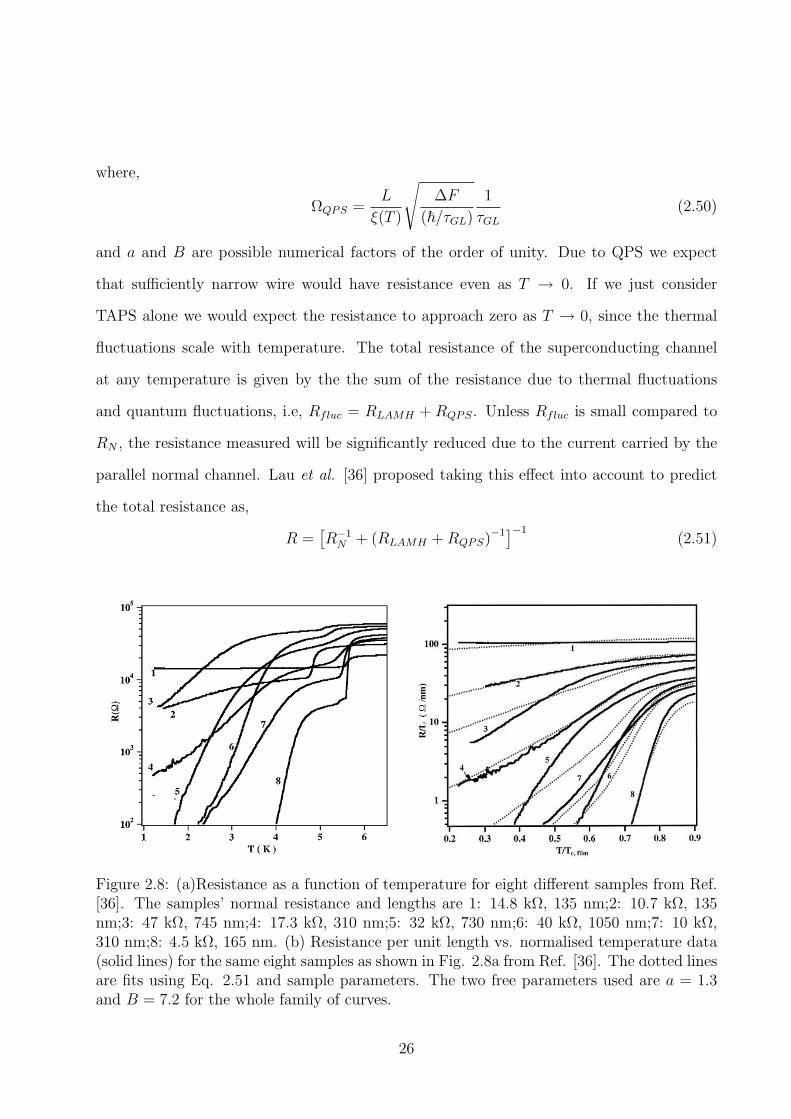
Figure 2.8: (a)Resistance as a function of temperature for eight different samples from Ref.[36]. The samples’ normal resistance and lengths are 1: 14.8 kΩ, 135 nm;2: 10.7 kΩ, 135nm;3: 47 kΩ, 745 nm;4: 17.3 kΩ, 310 nm;5: 32 kΩ, 730 nm;6: 40 kΩ, 1050 nm;7: 10 kΩ,310 nm;8: 4.5 kΩ, 165 nm. (b) Resistance per unit length vs. normalised temperature data(solid lines) for the same eight samples as shown in Fig. 2.8a from Ref. [36]. The dotted linesare fits using Eq. 2.51 and sample parameters. The two free parameters used are a = 1.3and B = 7.2 for the whole family of curves.
26
The group also performed measurements of a large number of amorphous MoGe wires
with various widths and lengths. They found a systematic broadening of the superconduct-
ing transition with decreasing cross-sectional areas, which can be described quantitatively
by a combination of thermally activated phase slips close to TC and QPS at low temper-
atures. Using a simple model with only two free parameters of order unity for the entire
family of curves, they found good agreement with the data over a wide range of samples.
These nanowires were formed by method of molecular templating using carbon nanotubes
(to be discussed in the next chapter). In this work over 20 samples were measured and a
representative set showing the resistance vs temperature data for eight different wires was
obtained (Fig. 2.8a from Ref. [36]). In contrast to this apparent simple dichotomy the R-T
curves in Fig. 2.8a display a broad spectrum of behaviors, including some superconducting
samples with resistance as high as 40 kΩ (≫ RQ). It indicates that the relevant parame-
ter controlling the superconducting transition is not the ratio of RQ/RN (as indicated by
Ref.[13]), but appears to be the resistance per unit length or equivalently, the cross-sectional
area. This is illustrated by the solid lines in Fig. 2.8b, which plots RL vs t ≡ T/TC,film.
Here t is the temperature normalized to film TC . The resistances of wider wires (RN/L < 20
Ω/nm) drop relatively sharply below TC,film. The transition widths broaden with increasing
values of RN/L, and resistances of the narrowest wires (RN/L > 80 Ω/nm) barely change
with temperature down to 1.5 K.
They found that the broad resistive transitions observed in the wires can not be described
by LAMH theory (Eq. 2.44) alone. To add the contribution of QPS they used the expression
for R of wire given by Eq. 2.51. To get the resistance due QPS the Eq. 2.49 was used.
This fits are shown as dotted lines in Fig. 2.8b. The most significant fact was that the
entire family of curves could be fitted with only one set of values for a and B (a = 1.3 and
B = 7.2).
A microscopic theory of QPS in nanowires was proposed by Golubev and Zaikin [37, 15]
using the renormalization theory. Within this model if the wire is short enough so that only
27
one phase slip event can happen at a time, we can neglect the effects of interaction of the
phase slips [38]. In this limit the QPS rate is given by,
ΓQPS =SQPS
τ0
L
ξexp(−SQPS) (2.52)
where the action SQPS is
SQPS = AGZ
(RQ
ξ
)(RN
L
)(2.53)
with AGZ being a numerical constant, RQ = h/4e2, and τ0 ∼ h/∆ is the characteristic re-
sponse time of a superconducting system that roughly determines the duration of each QPS,
ξ is the superconducting coherence length [15, 37]. The effective time averaged voltage Veff,
due to fluctuations, can be calculated from the QPS rate using the Josephson relationship.
Thus the effective resistance for nanowire due to QPS can be given by the expression,
RQPS ≡ Veff
I=hγQPS
2eI(2.54)
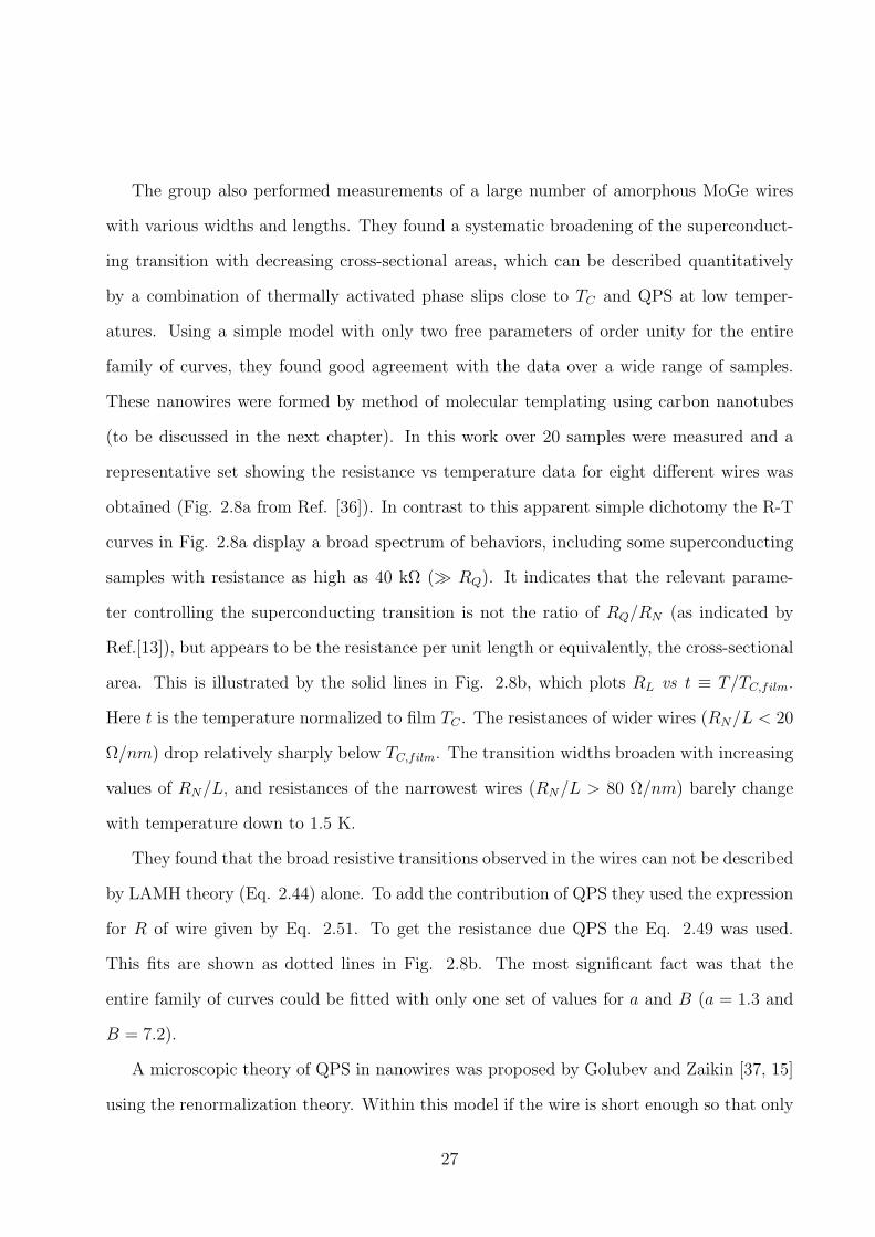
Zgirski et al.(Ref. [39]) found reasonable agreement of the data obtained from measure-
ment Al nanowires with the Golubev and Zaikin model. In their experiment, they started
with an Al nanowire with diameter√σ = 71 nm, fabricated conventional e-beam lithogra-
phy. The diameter of the wire was subsequently reduced by Ar+ ion sputtering (reduced
down to√σ = 8 nm). The resistance vs. temperature data for a Al nanowire whose diam-
eter was reduced after each measurement is shown in Fig. 2.9. They found that for thicker
wires for larger effective cross section diameters from√σ > 17 nm), the R(T ) dependencies
follow the same qualitative behavior: relatively narrow transition with quasi-linear slope
in logarithmic scale. These experimental data can be fitted with a reasonable accuracy by
theoretical calculations within the model of thermally activated phase slips (fits not shown).
But for thinner wires with diameters ∼ 11 nm or smaller, the transitions become wider and
the data can not be fitted alone the theory of TAPS with ant reasonable set of parameters
28
Figure 2.9: Resistance vs temperature for the same wire of length L = 10 µm after severalsputtering sessions from Ref. [39]. The sample and the measurement parameters are listed inthe table. For low-Ohmic samples, lock-in AC measurements with the front-end preamplifierwith input impedance 100 kΩ were used; for resistance above 500Ω they used DC nanovoltpreamplifier with input impedance 1 GΩ. The absence of data for the σ = 11 nm sample atT = 1.6 K was due to switching from DC to AC setup. There is a qualitative difference ofR(T ) dependencies for the two thinnest wires from the thicker ones.
(see Fig. 2.10). But they got agreement with the model of QPS proposed by Golubev and
Zaikin (Eq. 2.52) as shown in Fig. 2.10.
In their subsequent work, Zgirski et al. (Ref. [38]) showed that with the progressive
reduction on a particular Al nanowire, the gradual broadening of the resistive transition that
could be explained with the model of Golubev-Zaikin (using Eq. 2.52 and Eq. 2.54). The
resistance vs temperature data for the thinnest samples for the same Al nanowire obtained
by progressive reduction of the diameter is shown in Fig. 2.11. The length of the nanowire
L is 10 µm. The best fit with LAMH model is shown in for 2 nanowire samples. Clearly,
LAMH model can not explain the data, however the fitting done using Eq. 2.52 and Eq.
2.54, gives reasonable agreement.
29
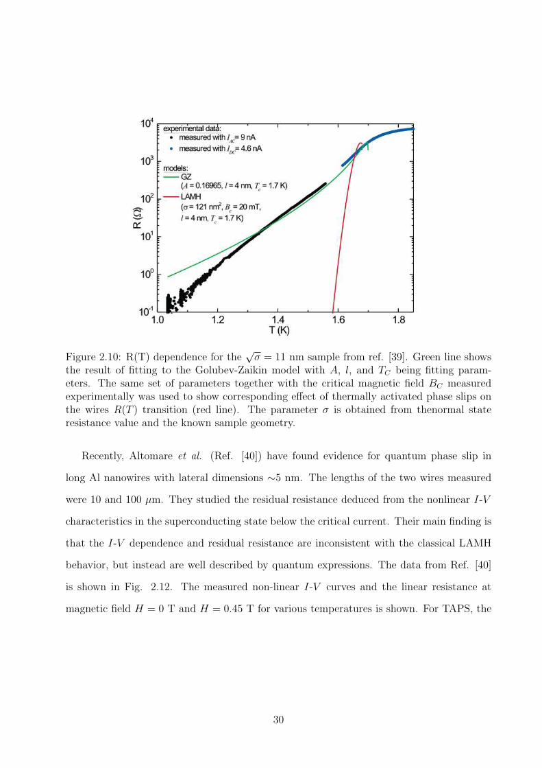
Figure 2.10: R(T) dependence for the√σ = 11 nm sample from ref. [39]. Green line shows
the result of fitting to the Golubev-Zaikin model with A, l, and TC being fitting param-eters. The same set of parameters together with the critical magnetic field BC measuredexperimentally was used to show corresponding effect of thermally activated phase slips onthe wires R(T ) transition (red line). The parameter σ is obtained from thenormal stateresistance value and the known sample geometry.
Recently, Altomare et al. (Ref. [40]) have found evidence for quantum phase slip in
long Al nanowires with lateral dimensions ∼5 nm. The lengths of the two wires measured
were 10 and 100 µm. They studied the residual resistance deduced from the nonlinear I-V
characteristics in the superconducting state below the critical current. Their main finding is
that the I-V dependence and residual resistance are inconsistent with the classical LAMH
behavior, but instead are well described by quantum expressions. The data from Ref. [40]
is shown in Fig. 2.12. The measured non-linear I-V curves and the linear resistance at
magnetic field H = 0 T and H = 0.45 T for various temperatures is shown. For TAPS, the
30
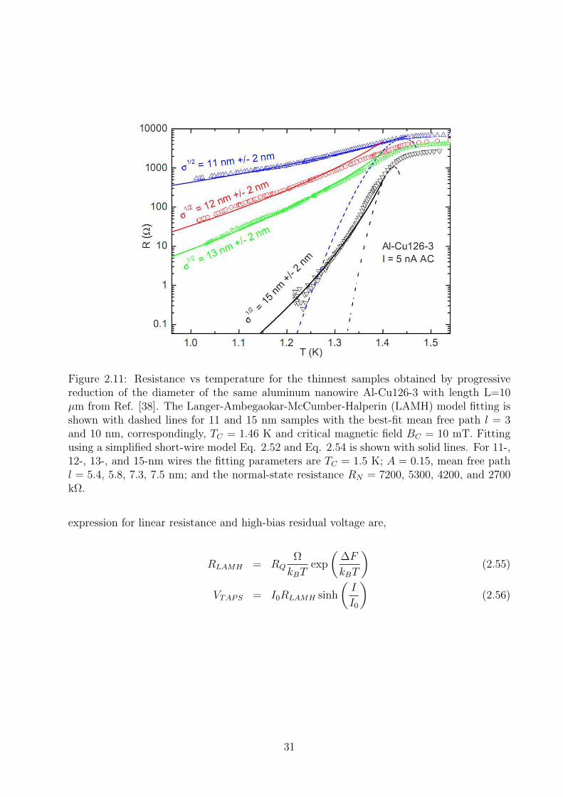
Figure 2.11: Resistance vs temperature for the thinnest samples obtained by progressivereduction of the diameter of the same aluminum nanowire Al-Cu126-3 with length L=10µm from Ref. [38]. The Langer-Ambegaokar-McCumber-Halperin (LAMH) model fitting isshown with dashed lines for 11 and 15 nm samples with the best-fit mean free path l = 3and 10 nm, correspondingly, TC = 1.46 K and critical magnetic field BC = 10 mT. Fittingusing a simplified short-wire model Eq. 2.52 and Eq. 2.54 is shown with solid lines. For 11-,12-, 13-, and 15-nm wires the fitting parameters are TC = 1.5 K; A = 0.15, mean free pathl = 5.4, 5.8, 7.3, 7.5 nm; and the normal-state resistance RN = 7200, 5300, 4200, and 2700kΩ.
expression for linear resistance and high-bias residual voltage are,
RLAMH = RQΩ
kBTexp
(∆F
kBT
)(2.55)
VTAPS = I0RLAMH sinh
(I
I0
)(2.56)
31
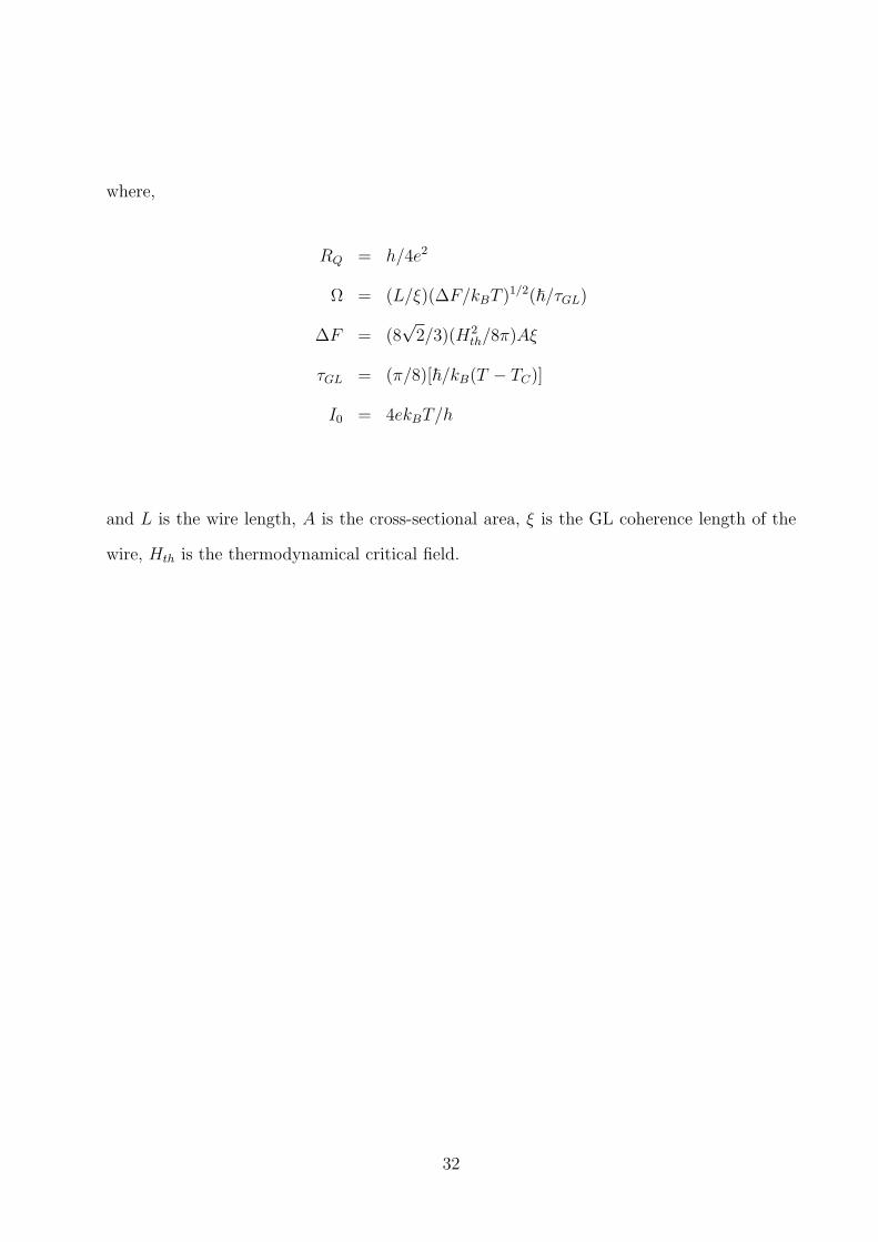
where,
RQ = h/4e2
Ω = (L/ξ)(∆F/kBT )1/2(~/τGL)
∆F = (8√
2/3)(H2th/8π)Aξ
τGL = (π/8)[~/kB(T − TC)]
I0 = 4ekBT/h
and L is the wire length, A is the cross-sectional area, ξ is the GL coherence length of the
wire, Hth is the thermodynamical critical field.
32
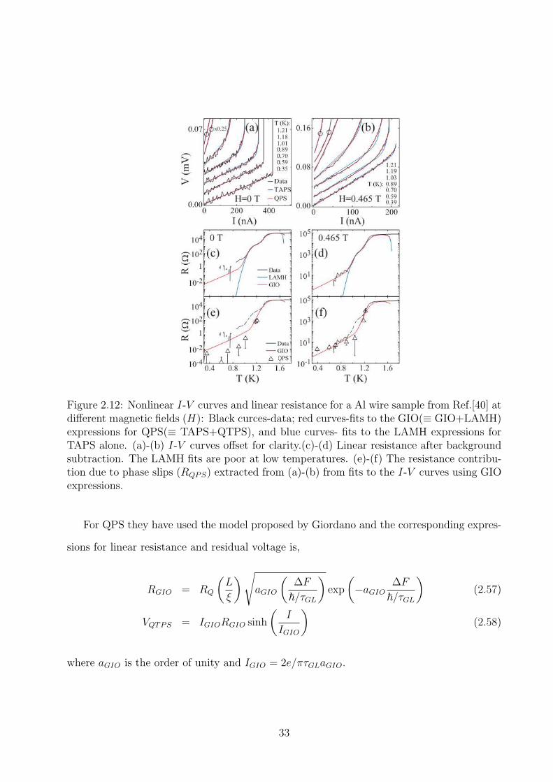
Figure 2.12: Nonlinear I-V curves and linear resistance for a Al wire sample from Ref.[40] atdifferent magnetic fields (H): Black curces-data; red curves-fits to the GIO(≡ GIO+LAMH)expressions for QPS(≡ TAPS+QTPS), and blue curves- fits to the LAMH expressions forTAPS alone. (a)-(b) I-V curves offset for clarity.(c)-(d) Linear resistance after backgroundsubtraction. The LAMH fits are poor at low temperatures. (e)-(f) The resistance contribu-tion due to phase slips (RQPS) extracted from (a)-(b) from fits to the I-V curves using GIOexpressions.
For QPS they have used the model proposed by Giordano and the corresponding expres-
sions for linear resistance and residual voltage is,
RGIO = RQ
(L
ξ
)√aGIO
(∆F
~/τGL
)exp
(−aGIO
∆F
~/τGL
)(2.57)
VQTPS = IGIORGIO sinh
(I
IGIO
)(2.58)
where aGIO is the order of unity and IGIO = 2e/πτGLaGIO.
33
Chapter 3
Fabrication and transport
measurements of superconducting
nanowires
We fabricate our nanowires using the method of molecular templating [13]. This method em-
ploys a suspended linear molecule as a template subjected to a thin layer of metal deposition
to produce a quasi -one-dimensional system. Superconducting wires have been fabricated in
the past by a number of different means. Some of the earliest work relied on using single crys-
tals of tin, known as whiskers, to study one-dimensional superconductivity [32, 33]. These
whiskers were of the order of ∼ 50 µm, which make them one-dimensional at temperatures
close to TC . As fabrication technology improved, wires of increasingly smaller cross-sectional
area were made using step edge [35] and stencil mask techniques [41]. These methods hinted
at possible quantum effects, such as quantum phase slips [35]and quantum phase transition,
such as metal-insulator transition[41] , which may exist in superconducting wires of reduced
dimensions.
To make wires with diameters that are small enough [15] (< 10 nm) to explore these
quantum effects we have used the method of molecular templating which has been exten-
sively developed in our group [13, 42, 28]. The basic idea behind this technique is to deposit
superconducting metal onto a free-standing molecule. Several molecules used as templates
include carbon nanotubes [13, 36], fluorinated carbon nanotubes [43, 44], DNA molecules
[42, 45], and WS2 nanorods [46]. Since the width of a molecule is on the order of a nanometer,
the wire formed on top of the molecule will have a comparable width. The molecule should
be rigid, straight and stable enough to withstand the metal deposition process. The molecule
should have good adhesion property with the metal to produce homogeneous nanowires free
from defects such as granularity. This method has the advantage that the diameter of the
34
wire depends on the amount of deposited material, which is a quantity that is easily con-
trolled during the sputtering process. Also, many wires are fabricated on the same substrate,
allowing us to choose the best (based on apparent homogeneity, desired dimensions, etc.)
for measurement. It should be noted that this technique is not limited to making supercon-
ducting wires – by using different metals (and perhaps an appropriate sticking layer) normal
metal and ferromagnetic wires can also be fabricated [47].
3.1 Fabrication of superconducting nanowires on top
of carbon nanotubes
3.1.1 Preparation of the substrate
In our method for fabricating superconducting nanowires, the first step is to prepare a
substrate that has a trench of ∼100-500 nm wide for deposition of free-standing molecules
as templates. We begin with a 4 inch in diameter and 500 µm thick Si-100 wafer. On
the wafer a layer constituting of a 0.5 µm SiO2 grown by dry (0.1 µm) and wet (0.4 µm)
oxidation. On top of it, 60 nm low stress SiN layer is deposited by low-pressure chemical
vapor deposition. The wafer is coated with an e-beam sensitive resist (PMMA). The entire
wafer is written with fine lines (widths of ∼100 nm) spaced at a distance of 4.8 mm . To
locate the nanowires on the trench during the fabrication process, numbered markers are
placed off to the side the lines that can be easily seen in an optical microscope. In order to
to explore the properties nanowires with different lengths, patterns with line widths of 50,
100, and 450 nm were used. The numbered markers are spaced 20 µm apart, so we have
∼240 markers in a 4.8 mm long chip.
After developing the patterns parts of the SiN layer are exposed and the pattern is
transferred into this SiN layer by reactive ion etching(RIE) using a SF6 plasma in Uniaxis
790 series reactive ion etching system. The e-beam resist is subsequently removed with
35
(a)
(b)
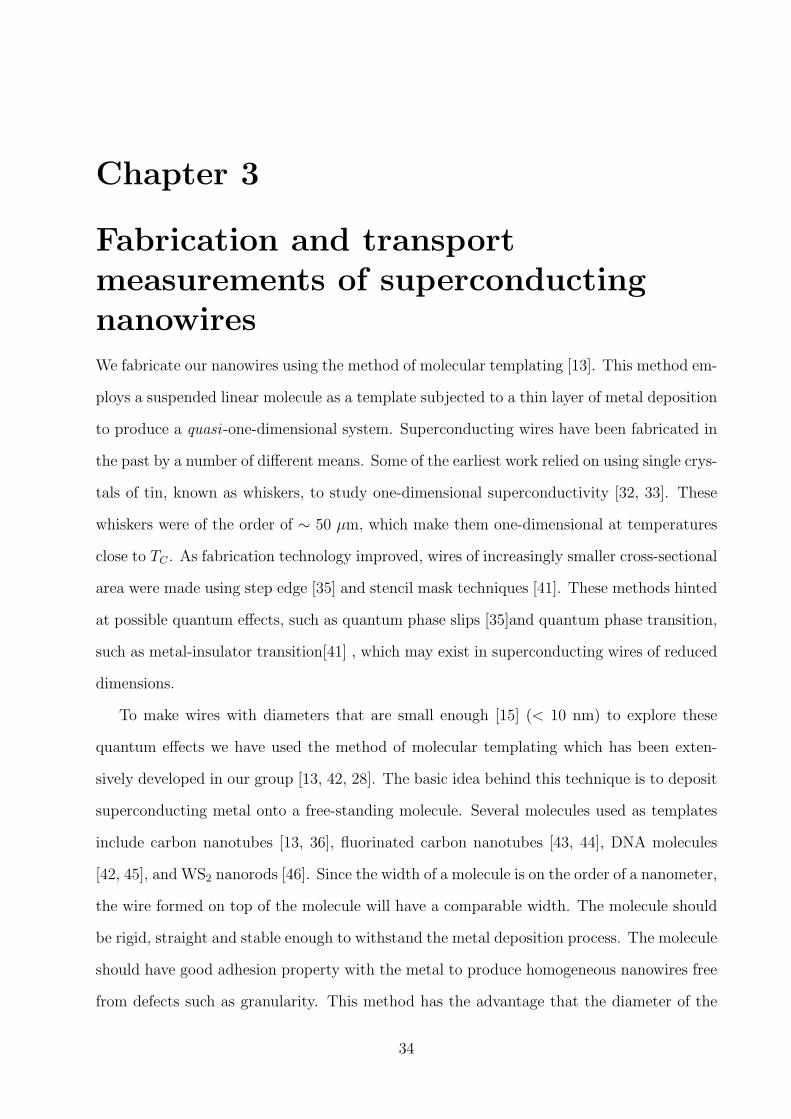
Figure 3.1: Preparation of the substrate: (a) Si(0.5 mm)-SiO2(500 nm)-SiN(60 nm) substratewith 50-500 nm wide trench defined by e-beam lithography and etch in SF6 plasma. (b)Substrate with a under-cut in the SiO2 layer produced by HF dip which etches SiO2 fasterthan SiN.
acetone and the entire wafer is coated with photoresist (AZ5214). An automated dicing saw
is used to cut the wafer into individual 4.8 mm × 4.8 mm patterned chips. The previous
photoresist deposition ensures that the SiN layer is protected from the silicon “dust” created
by the dicing. After dicing, this silicon dust can be easily removed along with the photoresist.
To remove the photoresist we sonicate the chip in acetone for 5 min. followed by rinsing in
deionized water for ∼30 sec. The chip is then sonicated in nitric acid for 5 min. followed by
another rinse in deionized water for ∼30 sec. At this point (Fig. 3.1a) the chip is immersed
in hydrofluoric acid for 10 sec. which creates an undercut in the SiO2 layer due to the
much greater etching rate of SiO2 compared to SiN (Fig. 3.1b). This is followed by rinsing
in deionized water for ∼30 sec., soaking in nitric acid for 2 min. to remove any residual
organics, rinsing in deionized water for ∼30 sec, rinsing in isopropanol for ∼30 sec., and
36
then blowing the chip dry with forced nitrogen gas.
3.1.2 Deposition of fluorinated single walled carbon nanotubes
We have used fluorinated single walled carbon nanotubes (FSWNTs) as templates for fab-
rication of our nanowires. These molecules are ideal templates for wires as they are known
to be insulating [48], which eliminates any possible conduction channel in parallel with the
nanowire. The insulating nature of the FSWNTs insures that we do not place any dissipa-
tive environment in close proximity with the wires that could affect any quantum phase slip
processes. The FSWNTs can also be easily dissolved in isopropanol, which makes deposit-
ing them from solution rather simple. These nanotubes are commercially available (Carbon
Nanotechnologies, Inc.) to be easily acquired and do not need to be grown by the user.
When starting with FSWNTs as received from the manufacturer the first step is to make
a “master”solution. This is prepared by sonicating a small piece (about 1 mm3) of bulk
FSWNTs in isopropanol (about 12 ml) for 20 min. The sonication will help to break up the
FSWNT clusters and promote their dissolving. After sonication the master solution should
be nearly transparent with a slight grey color to it. If any visible clusters of FSWNTs remain,
the solution should be further sonicated before using.
A separate diluted solution can be obtained from the master solution for depositing
FSWNTs. If the master solution has been stored for some time it is recommended that the
solution be sonicated for about 5 min. to ensure the FSWNTs are well dispersed before
making the diluted solution. A typical dilution is 1:5 to 1:20 parts master solution to
isopropanol by volume, though this can vary somewhat depending on how rich the master
solution was made. The dilution is tested by making a diluted solution, depositing a drop
of it onto a chip with a trench in it, letting the drop sit for 1 min., blowing the excess off
with forced nitrogen gas, and then examining the chip under an SEM. We ideally want one
nanotube crossing the trench about every 20 µm or one marker. This allows for an easier
alignment during photolithography steps. Once we have calibrated the proper dilution we
37
(a)
(b)
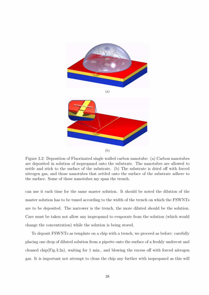
Figure 3.2: Deposition of Fluorinated single walled carbon nanotube: (a) Carbon nanotubesare deposited in solution of isopropanol onto the substrate. The nanotubes are allowed tosettle and stick to the surface of the substrate. (b) The substrate is dried off with forcednitrogen gas, and those nanotubes that settled onto the surface of the substrate adhere tothe surface. Some of these nanotubes my span the trench.
can use it each time for the same master solution. It should be noted the dilution of the
master solution has to be tuned according to the width of the trench on which the FSWNTs
are to be deposited. The narrower is the trench, the more diluted should be the solution.
Care must be taken not allow any isopropanol to evaporate from the solution (which would
change the concentration) while the solution is being stored.
To deposit FSWNTs as template on a chip with a trench, we proceed as before: carefully
placing one drop of diluted solution from a pipette onto the surface of a freshly undercut and
cleaned chip(Fig.3.2a), waiting for 1 min., and blowing the excess off with forced nitrogen
gas. It is important not attempt to clean the chip any further with isopropanol as this will
38
remove the FSWNTs that we have just deposited. Since the length of the FSWNTs is of the
order of a few microns or more some will be deposited to one side or the other of the trench
but some will be found across the trench providing templates for the nanowires(Fig.3.2b).
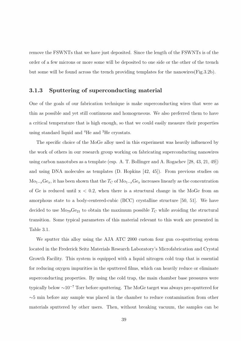
3.1.3 Sputtering of superconducting material
One of the goals of our fabrication technique is make superconducting wires that were as
thin as possible and yet still continuous and homogeneous. We also preferred them to have
a critical temperature that is high enough, so that we could easily measure their properties
using standard liquid and 4He and 3He cryostats.
The specific choice of the MoGe alloy used in this experiment was heavily influenced by
the work of others in our research group working on fabricating superconducting nanowires
using carbon nanotubes as a template (esp. A. T. Bollinger and A. Rogachev [28, 43, 21, 49])
and using DNA molecules as templates (D. Hopkins [42, 45]). From previous studies on
Mo1−xGex, it has been shown that the TC of Mo1−xGex increases linearly as the concentration
of Ge is reduced until x < 0.2, when there is a structural change in the MoGe from an
amorphous state to a body-centered-cubic (BCC) crystalline structure [50, 51]. We have
decided to use Mo79Ge21 to obtain the maximum possible TC while avoiding the structural
transition. Some typical parameters of this material relevant to this work are presented in
Table 3.1.
We sputter this alloy using the AJA ATC 2000 custom four gun co-sputtering system
located in the Frederick Seitz Materials Research Laboratory’s Microfabrication and Crystal
Growth Facility. This system is equipped with a liquid nitrogen cold trap that is essential
for reducing oxygen impurities in the sputtered films, which can heavily reduce or eliminate
superconducting properties. By using the cold trap, the main chamber base pressures were
typically below ∼10−7 Torr before sputtering. The MoGe target was always pre-sputtered for
∼5 min before any sample was placed in the chamber to reduce contamination from other
materials sputtered by other users. Then, without breaking vacuum, the samples can be
39
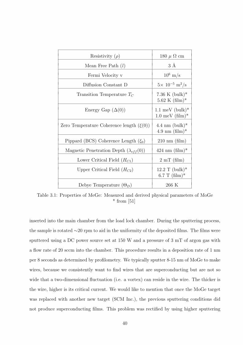
Resistivity (ρ) 180 µ Ω cm
Mean Free Path (l) 3 A
Fermi Velocity v 106 m/s
Diffusion Constant D 5× 10⁻⁵ m2/s
Transition Temperature TC 7.36 K (bulk)*5.62 K (film)*
Energy Gap (∆(0)) 1.1 meV (bulk)*1.0 meV (film)*
Zero Temperature Coherence length (ξ(0)) 4.4 nm (bulk)*4.9 nm (film)*
Pippard (BCS) Coherence Length (ξ0) 210 nm (film)
Magnetic Penetration Depth (λeff (0)) 424 nm (film)*
Lower Critical Field (HC1) 2 mT (film)
Upper Critical Field (HC2) 12.2 T (bulk)*6.7 T (film)*
Debye Temperature (ΘD) 266 K
Table 3.1: Properties of MeGe: Measured and derived physical parameters of MoGe* from [51]
inserted into the main chamber from the load lock chamber. During the sputtering process,
the sample is rotated ∼20 rpm to aid in the uniformity of the deposited films. The films were
sputtered using a DC power source set at 150 W and a pressure of 3 mT of argon gas with
a flow rate of 20 sccm into the chamber. This procedure results in a deposition rate of 1 nm
per 8 seconds as determined by profilometry. We typically sputter 8-15 nm of MoGe to make
wires, because we consistently want to find wires that are superconducting but are not so
wide that a two-dimensional fluctuation (i.e. a vortex) can reside in the wire. The thicker is
the wire, higher is its critical current. We would like to mention that once the MoGe target
was replaced with another new target (SCM Inc.), the previous sputtering conditions did
not produce superconducting films. This problem was rectified by using higher sputtering
40
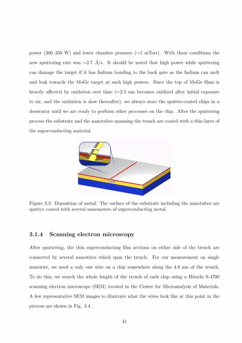
power (300–350 W) and lower chamber pressure (∼1 mTorr). With these conditions the
new sputtering rate was ∼2.7 A/s. It should be noted that high power while sputtering
can damage the target if it has Indium bonding to the back gate as the Indium can melt
and leak towards the MoGe target at such high powers. Since the top of MoGe films is
heavily affected by oxidation over time (∼2.5 nm becomes oxidized after initial exposure
to air, and the oxidation is slow thereafter), we always store the sputter-coated chips in a
dessicator until we are ready to perform other processes on the chip. After the sputtering
process the substrate and the nanotubes spanning the trench are coated with a thin layer of
the superconducting material.
Figure 3.3: Deposition of metal: The surface of the substrate including the nanotubes aresputter coated with several nanometers of superconducting metal.
3.1.4 Scanning electron microscopy
After sputtering, the thin superconducting film sections on either side of the trench are
connected by several nanowires which span the trench. For our measurement on single
nanowire, we need a only one wire on a chip somewhere along the 4.8 nm of the trench.
To do this, we search the whole length of the trench of each chip using a Hitachi S-4700
scanning electron microscope (SEM) located in the Center for Microanalysis of Materials.
A few representative SEM images to illustrate what the wires look like at this point in the
process are shown in Fig. 3.4 .
41
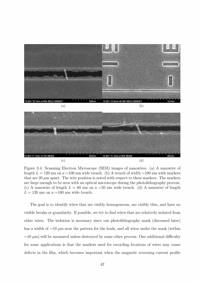
(a) (b)
(c) (d)
Figure 3.4: Scanning Electron Microscope (SEM) images of nanowires. (a) A nanowire oflength L = 120 nm on a ∼100 nm wide trench. (b) A trench of width ∼100 nm with markersthat are 20 µm apart. The wire position is noted with respect to these markers. The markersare large enough to be seen with an optical microscope during the photolithography process.(c) A nanowire of length L = 80 nm on a ∼50 nm wide trench. (d) A nanowire of lengthL = 120 nm on a ∼100 nm wide trench.
The goal is to identify wires that are visibly homogeneous, are visibly thin, and have no
visible breaks or granularity. If possible, we try to find wires that are relatively isolated from
other wires. The isolation is necessary since our photolithography mask (discussed later)
has a width of ∼10 µm near the pattern for the leads, and all wires under the mask (within
∼10 µm) will be measured unless destroyed by some other process. One additional difficulty
for some applications is that the markers used for recording locations of wires may cause
defects in the film, which becomes important when the magnetic screening current profile
42
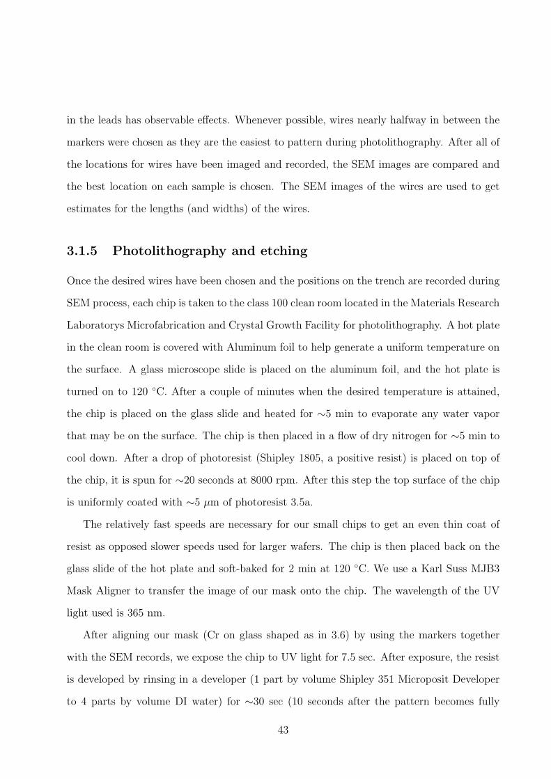
in the leads has observable effects. Whenever possible, wires nearly halfway in between the
markers were chosen as they are the easiest to pattern during photolithography. After all of
the locations for wires have been imaged and recorded, the SEM images are compared and
the best location on each sample is chosen. The SEM images of the wires are used to get
estimates for the lengths (and widths) of the wires.
3.1.5 Photolithography and etching
Once the desired wires have been chosen and the positions on the trench are recorded during
SEM process, each chip is taken to the class 100 clean room located in the Materials Research
Laboratorys Microfabrication and Crystal Growth Facility for photolithography. A hot plate
in the clean room is covered with Aluminum foil to help generate a uniform temperature on
the surface. A glass microscope slide is placed on the aluminum foil, and the hot plate is
turned on to 120 C. After a couple of minutes when the desired temperature is attained,
the chip is placed on the glass slide and heated for ∼5 min to evaporate any water vapor
that may be on the surface. The chip is then placed in a flow of dry nitrogen for ∼5 min to
cool down. After a drop of photoresist (Shipley 1805, a positive resist) is placed on top of
the chip, it is spun for ∼20 seconds at 8000 rpm. After this step the top surface of the chip
is uniformly coated with ∼5 µm of photoresist 3.5a.
The relatively fast speeds are necessary for our small chips to get an even thin coat of
resist as opposed slower speeds used for larger wafers. The chip is then placed back on the
glass slide of the hot plate and soft-baked for 2 min at 120 C. We use a Karl Suss MJB3
Mask Aligner to transfer the image of our mask onto the chip. The wavelength of the UV
light used is 365 nm.
After aligning our mask (Cr on glass shaped as in 3.6) by using the markers together
with the SEM records, we expose the chip to UV light for 7.5 sec. After exposure, the resist
is developed by rinsing in a developer (1 part by volume Shipley 351 Microposit Developer
to 4 parts by volume DI water) for ∼30 sec (10 seconds after the pattern becomes fully
43
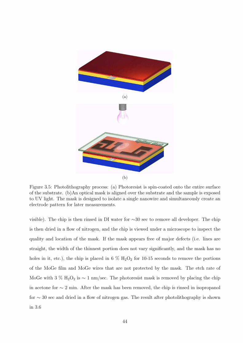
(a)
(b)
Figure 3.5: Photolithography process: (a) Photoresist is spin-coated onto the entire surfaceof the substrate. (b)An optical mask is aligned over the substrate and the sample is exposedto UV light. The mask is designed to isolate a single nanowire and simultaneously create anelectrode pattern for later measurements.
visible). The chip is then rinsed in DI water for ∼30 sec to remove all developer. The chip
is then dried in a flow of nitrogen, and the chip is viewed under a microscope to inspect the
quality and location of the mask. If the mask appears free of major defects (i.e. lines are
straight, the width of the thinnest portion does not vary significantly, and the mask has no
holes in it, etc.), the chip is placed in 6 % H2O2 for 10-15 seconds to remove the portions
of the MoGe film and MoGe wires that are not protected by the mask. The etch rate of
MoGe with 3 % H2O2 is ∼ 1 nm/sec. The photoresist mask is removed by placing the chip
in acetone for ∼ 2 min. After the mask has been removed, the chip is rinsed in isopropanol
for ∼ 30 sec and dried in a flow of nitrogen gas. The result after photolithography is shown
in 3.6
44
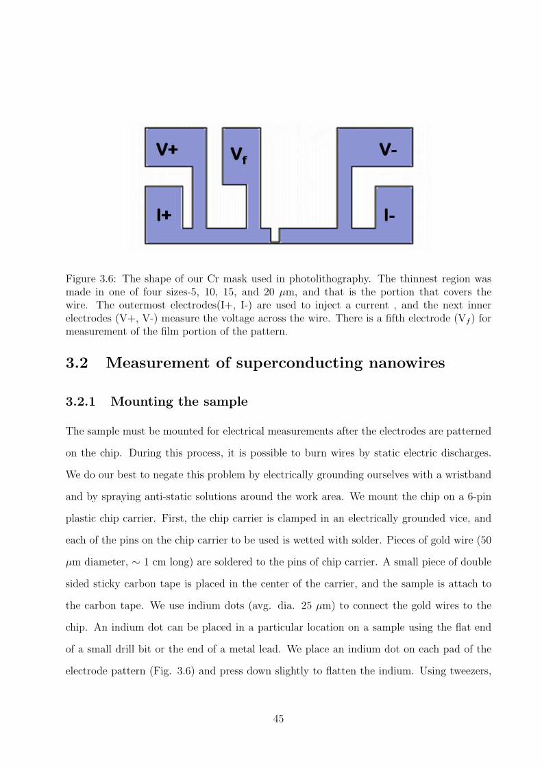
Figure 3.6: The shape of our Cr mask used in photolithography. The thinnest region wasmade in one of four sizes-5, 10, 15, and 20 µm, and that is the portion that covers thewire. The outermost electrodes(I+, I-) are used to inject a current , and the next innerelectrodes (V+, V-) measure the voltage across the wire. There is a fifth electrode (Vf ) formeasurement of the film portion of the pattern.
3.2 Measurement of superconducting nanowires
3.2.1 Mounting the sample
The sample must be mounted for electrical measurements after the electrodes are patterned
on the chip. During this process, it is possible to burn wires by static electric discharges.
We do our best to negate this problem by electrically grounding ourselves with a wristband
and by spraying anti-static solutions around the work area. We mount the chip on a 6-pin
plastic chip carrier. First, the chip carrier is clamped in an electrically grounded vice, and
each of the pins on the chip carrier to be used is wetted with solder. Pieces of gold wire (50
µm diameter, ∼ 1 cm long) are soldered to the pins of chip carrier. A small piece of double
sided sticky carbon tape is placed in the center of the carrier, and the sample is attach to
the carbon tape. We use indium dots (avg. dia. 25 µm) to connect the gold wires to the
chip. An indium dot can be placed in a particular location on a sample using the flat end
of a small drill bit or the end of a metal lead. We place an indium dot on each pad of the
electrode pattern (Fig. 3.6) and press down slightly to flatten the indium. Using tweezers,
45
a gold wire attached to a pin is moved over the indium dot, and a second indium dot is
flattened over the gold wire. The result is a gold wire sandwiched between two indium dots
and connected to a pad. This helps maintain a good electrical contact and minimizes the
possibility that the gold wire will become detached when the sample is cooled.
3.2.2 Cryostats
Once all the pads on the chips to be used are connected to the chip carrier using the gold
wires, the chip carriers are inserted into a socket on one of three cryostats. One of the
cryostats is designed for inserting samples into 4He transfer dewars, and we can measure
down to temperatures of ∼1.35 K using this 4He system. Another cryostat is a standard 3He
cryostat, and we can measure down to ∼0.27 K using this 3He system. The dewar for the
3He system is also equipped with a magnet allowing us to generate magnetic fields up to 9 T.
For measurements at the lowest temperatures, an insert was used for a top loading Oxford
Instruments Kelvinox dilution refrigerator that is located in Dale van Harlingens laboratory
and maintained by his research group.
The 4He system is the most basic system that we use for measurements as it easy to
use, inexpensive and the sample can be quickly measured down to 1.35 K. The 4He system
was built by U. C. Coskun in our laboratory. The details about this dipstick can be found
in Ref. [52]. In the dipstick, a socket for the chip carriers is located at the bottom of the
dipstick. There are ten measurement leads that run from the room temperature portion
of the stick down to the bottom and are connected thermally to a copper block by silver
paste. The silver paste also serves as a filter for high frequency noise. The temperature is
measured by measuring the resistance of a calibrated Cernox thermometer, to which four
of the measurement leads are attached, located next to the socket on the copper plate. A
copper can covers the sample and thermometer, and it is wound with resistive twisted pair
wire(Stableohm) which serve as a heater. A stainless steel pipe covers the length of the
dipstick so that a vacuum can be created around the sample. Once a sample to be measured
46
has been placed in the socket, the air in the dipstick is evacuated at room temperature, and
a small amount of He gas (as exchange gas) is introduced to help in the cooling process.
The bottom portion of the stick is immersed in liquid nitrogen until it cools to 77 K. By
cooling first in liquid nitrogen, we save on the amount of liquid helium necessary to cool
the dipstick to 77 K from room temperature. We then transfer the dipstick into a 35-liter
capacity liquid He transfer dewar filled with ∼ 2 liters of liquid helium and let it cool. To
attain temperatures down to ∼1.35 K, we use a vacuum pump to slowly remove the He vapor
above the liquid helium bath which decreases the boiling point of liquid He. By pumping
on only a small volume of liquid helium (∼ 2 liters), we are able to quickly reduce the
temperature to ∼ 1.4 K in about a couple of hours. Once at this base temperature, we
can measure our samples for ∼ 12 hours before the liquid helium has completely evaporated.
Also, once at the base temperature the sample can be heated up to some desired temperature
with the help of the heater and a current source.
To achieve lower temperatures below 1.35 K for measurements, we use 3He system pur-
chased from Janis Research Company. In this system a ∼ 2 mm wide tube connects the
4He bath to a 1 K pot, allowing liquid 4He to enter at a controllable rate(with the help of
a valve). A vacuum pump can cool the pot to ∼ 1 K by removing the 4He vapor. The 1
K pot surrounds an inner tube containing 3He gas, which begins to condense once the 1 K
pot reaches a temperature below 2 K. The condensed 3He liquid collects in the 3He pot just
above the sample. Once all the 3He is condensed, the 3He vapor above it can be“pumped”
away by the sorption pumpcharcoals that bind He vapor when they are cold. By using this
sorption pump, we are able to remove the vapors without allowing 3He gas to leave our sys-
tem, and we can achieve temperature of ∼ 0.27 K. High resistance wires connect the room
temperature portion of the cryostat to the 1 K pot to minimize thermal coupling. More high
resistance wires connect from the 1 K pot to the 3He pot.A copper attachment connects the
3He pot and sockets for the thermometer and sample. Long low resistance wires are wound
around the copper attachment connected to the 3He pot and covered with silver paste as
47
a filter. These wires are then connected to the sample carrying sockets. Two sockets exist
in this system for different magnetic field orientations (perpendicular and parallel to the
film).The side socket which can hold upto two chips has a a calibrated ruthenium oxide
thermometer measured in a four-probe configuration. As mentioned before, the dewar for
this system is equipped with a magnet, which can generate fields up to 9 T.
3.2.3 Filtering system of 3He measurement setup
It is essential for us to minimize the high frequency noise(which if of the order of the QPS
rate) coming from the outside environment that would interact with the nanowire and lead to
noise in the acquired data and can be wrongly interpreted as QPS.In this section we discuss
the arrangement of RF filters in our 3He measurement setup. The purpose of these filters
is to suppress external high-frequency electromagnetic noise, such as the noise originating
from cell-phones, radio stations, and also the black-body radiation, which can, if filters are
not installed, propagate through the measurement leads and reach the sample and modify
the switching current observed in the experiment. Our filters are designed to reduce this
noise effect to a negligible level.
Our main filtering stage is a Copper powder filter thermalized at the base temperature
(0.29 K). The filter is of the type developed by Martinis, Devoret and Clarke [5]. More
details are presented below.
In our system, each signal line has three stages of filtering in series, namely, a π-filter at
room temperature and a copper-powder filter (Cu-F) (at the base temperature) and silver-
paste filter (Ag-F) (also, at the base temperature). These filters are necessary to suppress
noise ranging from low frequency to high microwave frequencies. The compact powder filters
(i.e., Cu-F or Ag-F) rely on the skin effect damping for attenuation of high frequencies. At
room temperature, commercially available π-filters (Spectrum Control, SCI 1201-066) are
placed on each electrical lead before they enter the cryostat. The π-filters are mounted inside
an aluminum box (Hammond Manufacturing) which is attached to the top of the cryostat.
48
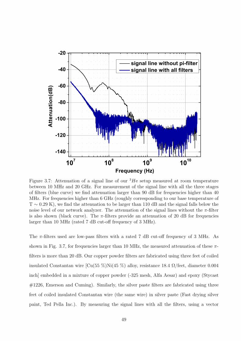
107 108 109 1010
-140
-120
-100
-80
-60
-40
-20
Atten
uatio
n(dB
)
Frequency (Hz)
signal line without pi-filter signal line with all filters
Figure 3.7: Attenuation of a signal line of our 3He setup measured at room temperaturebetween 10 MHz and 20 GHz. For measurement of the signal line with all the three stagesof filters (blue curve) we find attenuation larger than 90 dB for frequencies higher than 40MHz. For frequencies higher than 6 GHz (roughly corresponding to our base temperature ofT ∼ 0.29 K), we find the attenuation to be larger than 110 dB and the signal falls below thenoise level of our network analyzer. The attenuation of the signal lines without the π-filteris also shown (black curve). The π-filters provide an attenuation of 20 dB for frequencieslarger than 10 MHz (rated 7 dB cut-off frequency of 3 MHz).
The π-filters used are low-pass filters with a rated 7 dB cut-off frequency of 3 MHz. As
shown in Fig. 3.7, for frequencies larger than 10 MHz, the measured attenuation of these π-
filters is more than 20 dB. Our copper powder filters are fabricated using three feet of coiled
insulated Constantan wire [Cu(55 %)Ni(45 %) alloy, resistance 18.4 Ω/feet, diameter 0.004
inch] embedded in a mixture of copper powder (-325 mesh, Alfa Aesar) and epoxy (Stycast
#1226, Emerson and Cuming). Similarly, the silver paste filters are fabricated using three
feet of coiled insulated Constantan wire (the same wire) in silver paste (Fast drying silver
paint, Ted Pella Inc.). By measuring the signal lines with all the filters, using a vector
49
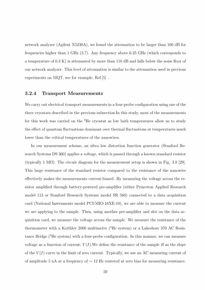
network analyzer (Agilent N5230A), we found the attenuation to be larger than 100 dB for
frequencies higher than 1 GHz (3.7). Any frequency above 6.25 GHz (which corresponds to
a temperature of 0.3 K) is attenuated by more than 110 dB and falls below the noise floor of
our network analyzer. This level of attenuation is similar to the attenuation used in previous
experiments on MQT, see for example, Ref.[5] .
3.2.4 Transport Measurements
We carry out electrical transport measurements in a four-probe configuration using one of the
three cryostats described in the previous subsection.In this study, most of the measurements
for this work was carried on the 3He cryostat as low bath temperatures allow us to study
the effect of quantum fluctuations dominant over thermal fluctuations at temperatures much
lower than the critical temperatures of the nanowires.
In our measurement scheme, an ultra low distortion function generator (Stanford Re-
search Systems DS 360) applies a voltage, which is passed through a known standard resistor
(typically 1 MΩ). The circuit diagram for the measurement setup is shown in Fig. 3.8 [29].
This large resistance of the standard resistor compared to the resistance of the nanowire
effectively makes the measurements current-biased. By measuring the voltage across the re-
sistor amplified through battery-powered pre-amplifier (either Princeton Applied Research
model 113 or Stanford Research Systems model SR 560) connected to a data acquisition
card (National Instruments model PCI-MIO-16XE-10), we are able to measure the current
we are applying to the sample. Then, using another pre-amplifier and slot on the data ac-
quisition card, we measure the voltage across the sample. We measure the resistance of the
thermometer with a Keithley 2000 multimeter (4He system) or a Lakeshore 370 AC Resis-
tance Bridge (3He system) with a four-probe configuration. In this manner, we can measure
voltage as a function of current, V (I).We define the resistance of the sample R as the slope
of the V (I) curve in the limit of zero current. Typically, we use an AC measuring current of
of amplitude 5 nA at a frequency of ∼ 12 Hz centered at zero bias for measuring resistance.
50
Figure 3.8: Schematic of the measurement setup for transport measurement of nanowires[29]. The sample is current-biased by a function generator with a 1 MΩ resistor in series. Thecurrent is measured by measuring the voltage across the standard resistor using a preamp.The sample voltage is measured using another preamp. The tempeartue of the sampleis measured using a caliberated thermometer measured in a four-probe configuration. Toreduce noise π-filters are employed at room temperature and Cu powder and Ag paste filtersare used at the base temperature.
Using a measuring current that is too low leads to a noisy measurement of R, and using
a measuring current that is too large gives an incorrect value of R if the V (I) curve is no
longer linear at high bias.
For measuring a V (I ) curve, the function generator is set at slow frequency of ∼ 5 mHz
and large amplitude that gives bias currents of the order of few µA (The amplitude of this
current is modulated depending upon the critical current of the nanowire). During these
51
measurements currents much larger than the critical current of the wires have a risk of
burning the wires. We also measure dV (I)/dI by measuring the slope of the V (I) curve in
a narrow range centered around a nonzero bias current. We can also measure any of these
parameters while altering magnetic fields and temperatures. For temperatures low enough
for a sample to be superconducting, we can also measure switching current ISW (the current at
which the sample jumps from a low-voltage state to a resistive state) and retrapping current
IR (the current at which a resistive wire returns to a low-voltage state). The temperatures
can be fixed during these measurements through a LabVIEW controlled feedback loop (4He
system) or a feedback loop (PID) controlling the heater output by the Lakeshore device (3He
system).
52
Chapter 4
Low-bias measurements of
superconducting nanowires
In this chapter I will discuss about low-biasR(T ) measurements performed on single nanowires
samples. By low-bias measurements we mean that the applied currents are much smaller
than the thermodynamic critical current such that the current-voltage (V (I)) characteristics
show Ohmic behavior. I will also discuss that for the superconducting wires the resistive
transitions can be well explained by theory of thermally activated phase slips (TAPS). To
obtain the fits I have used two models of TAPS, namely, Little fit and Langer, Ambegaokar,
McCumber and Halperin (LAMH) fit. An agreement of the resistance measured in an exper-
iment with that predicted in LAMH model would thus indicate homogeneity of the measured
wire. For the insulating wires only the R(T ) data will be shown for a few measured samples.
For the insulating wires only the R(T ) data will be shown for a few measured samples .
4.1 Resistance vs. temperature R(T ) curves
The resistance vs, temperature curve for nanowire measured in the 4He measurement set up
is shown in Fig. 4.1. As the wire is seamlessly connected in series with the film electrodes
we observe two resistive transitions, one corresponding to the film electrodes and the other
corresponding to the nanowire. The rather sharp transition ( at ∼6 K) is due to the film
electrodes becoming superconducting. The second transition (around ∼3.5 K) is due to the
nanowire going “superconducting”. Throughout this study the film and wire were sputtered
together, its found that the film always had a higher TC than the wire. The resistance of the
wire diminishes by three orders of magnitude and the resistance can be measured down to
53
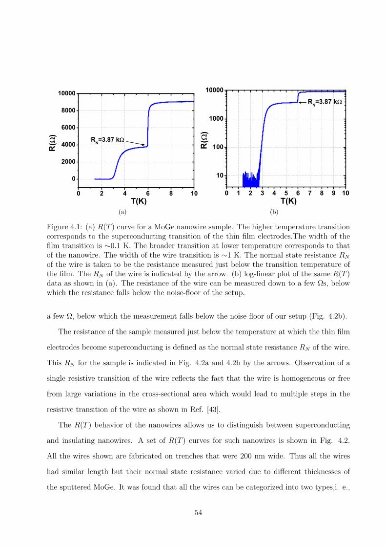
0 2 4 6 8 10
0
2000
4000
6000
8000
10000
R(
)
T(K)
RN=3.87 k
(a)
0 1 2 3 4 5 6 7 8 9 10
10
100
1000
10000
RN=3.87 k
R(
)T(K)
(b)
Figure 4.1: (a) R(T ) curve for a MoGe nanowire sample. The higher temperature transitioncorresponds to the superconducting transition of the thin film electrodes.The width of thefilm transition is ∼0.1 K. The broader transition at lower temperature corresponds to thatof the nanowire. The width of the wire transition is ∼1 K. The normal state resistance RN
of the wire is taken to be the resistance measured just below the transition temperature ofthe film. The RN of the wire is indicated by the arrow. (b) log-linear plot of the same R(T )data as shown in (a). The resistance of the wire can be measured down to a few Ωs, belowwhich the resistance falls below the noise-floor of the setup.
a few Ω, below which the measurement falls below the noise floor of our setup (Fig. 4.2b).
The resistance of the sample measured just below the temperature at which the thin film
electrodes become superconducting is defined as the normal state resistance RN of the wire.
This RN for the sample is indicated in Fig. 4.2a and 4.2b by the arrows. Observation of a
single resistive transition of the wire reflects the fact that the wire is homogeneous or free
from large variations in the cross-sectional area which would lead to multiple steps in the
resistive transition of the wire as shown in Ref. [43].
The R(T ) behavior of the nanowires allows us to distinguish between superconducting
and insulating nanowires. A set of R(T ) curves for such nanowires is shown in Fig. 4.2.
All the wires shown are fabricated on trenches that were 200 nm wide. Thus all the wires
had similar length but their normal state resistance varied due to different thicknesses of
the sputtered MoGe. It was found that all the wires can be categorized into two types,i. e.,
54
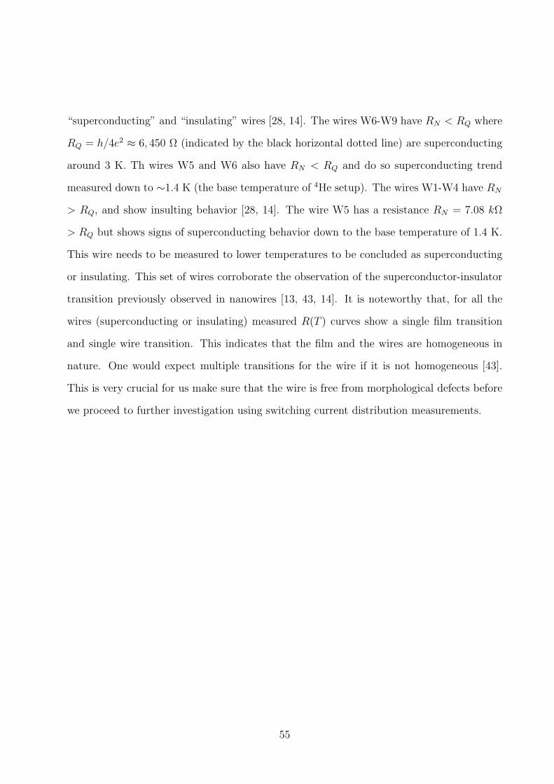
“superconducting” and “insulating” wires [28, 14]. The wires W6-W9 have RN < RQ where
RQ = h/4e2 ≈ 6, 450 Ω (indicated by the black horizontal dotted line) are superconducting
around 3 K. Th wires W5 and W6 also have RN < RQ and do so superconducting trend
measured down to ∼1.4 K (the base temperature of 4He setup). The wires W1-W4 have RN
> RQ, and show insulting behavior [28, 14]. The wire W5 has a resistance RN = 7.08 kΩ
> RQ but shows signs of superconducting behavior down to the base temperature of 1.4 K.
This wire needs to be measured to lower temperatures to be concluded as superconducting
or insulating. This set of wires corroborate the observation of the superconductor-insulator
transition previously observed in nanowires [13, 43, 14]. It is noteworthy that, for all the
wires (superconducting or insulating) measured R(T ) curves show a single film transition
and single wire transition. This indicates that the film and the wires are homogeneous in
nature. One would expect multiple transitions for the wire if it is not homogeneous [43].
This is very crucial for us make sure that the wire is free from morphological defects before
we proceed to further investigation using switching current distribution measurements.
55
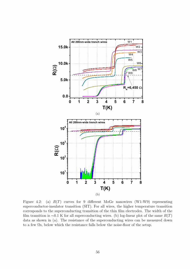
0 1 2 3 4 5 6 7 80.0
5.0k
10.0k
15.0k
W9W8 W7
W6W5
W4W3
W2
All 200nm-wide trench wires
R(
)
T(K)
W1
RN=6,450
(a)
0 1 2 3 4 5 6 7 8
101
102
103
104All 200nm-wide trench wires
R(
)
T(K)(b)
Figure 4.2: (a) R(T ) curves for 9 different MoGe nanowires (W1-W9) representingsuperconductor-insulator transition (SIT). For all wires, the higher temperature transitioncorresponds to the superconducting transition of the thin film electrodes. The width of thefilm transition is ∼0.1 K for all superconducting wires. (b) log-linear plot of the same R(T )data as shown in (a). The resistance of the superconducting wires can be measured downto a few Ωs, below which the resistance falls below the noise-floor of the setup.
56
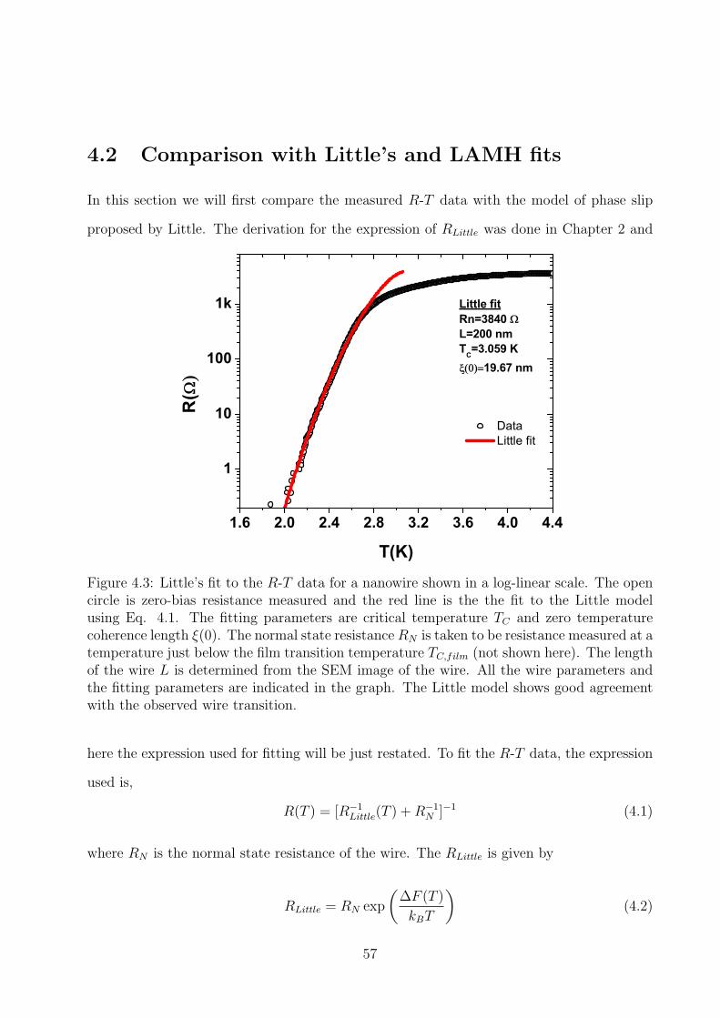
4.2 Comparison with Little’s and LAMH fits
In this section we will first compare the measured R-T data with the model of phase slip
proposed by Little. The derivation for the expression of RLittle was done in Chapter 2 and
1.6 2.0 2.4 2.8 3.2 3.6 4.0 4.4
1
10
100
1k
Data Little fit
Little fitRn=3840 L=200 nmTC=3.059 K
19.67 nm
R(
T(K)Figure 4.3: Little’s fit to the R-T data for a nanowire shown in a log-linear scale. The opencircle is zero-bias resistance measured and the red line is the the fit to the Little modelusing Eq. 4.1. The fitting parameters are critical temperature TC and zero temperaturecoherence length ξ(0). The normal state resistance RN is taken to be resistance measured at atemperature just below the film transition temperature TC,film (not shown here). The lengthof the wire L is determined from the SEM image of the wire. All the wire parameters andthe fitting parameters are indicated in the graph. The Little model shows good agreementwith the observed wire transition.
here the expression used for fitting will be just restated. To fit the R-T data, the expression
used is,
R(T ) = [R−1Little(T ) +R−1
N ]−1 (4.1)
where RN is the normal state resistance of the wire. The RLittle is given by
RLittle = RN exp
(∆F (T )
kBT
)(4.2)
57
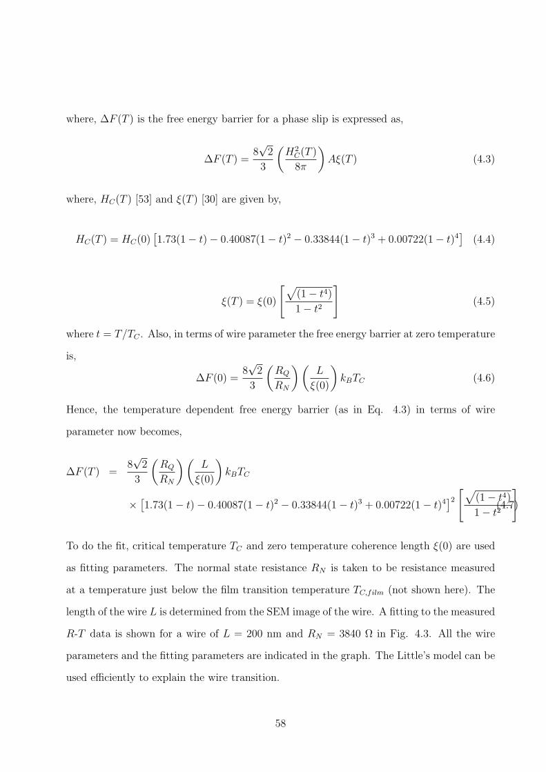
where, ∆F (T ) is the free energy barrier for a phase slip is expressed as,
∆F (T ) =8√
2
3
(H2
C(T )
8π
)Aξ(T ) (4.3)
where, HC(T ) [53] and ξ(T ) [30] are given by,
HC(T ) = HC(0)[1.73(1 − t) − 0.40087(1 − t)2 − 0.33844(1 − t)3 + 0.00722(1 − t)4
](4.4)
ξ(T ) = ξ(0)
[√(1 − t4)
1 − t2
](4.5)
where t = T/TC . Also, in terms of wire parameter the free energy barrier at zero temperature
is,
∆F (0) =8√
2
3
(RQ
RN
)(L
ξ(0)
)kBTC (4.6)
Hence, the temperature dependent free energy barrier (as in Eq. 4.3) in terms of wire
parameter now becomes,
∆F (T ) =8√
2
3
(RQ
RN
)(L
ξ(0)
)kBTC
×[1.73(1 − t) − 0.40087(1 − t)2 − 0.33844(1 − t)3 + 0.00722(1 − t)4
]2[√
(1 − t4)
1 − t2
](4.7)
To do the fit, critical temperature TC and zero temperature coherence length ξ(0) are used
as fitting parameters. The normal state resistance RN is taken to be resistance measured
at a temperature just below the film transition temperature TC,film (not shown here). The
length of the wire L is determined from the SEM image of the wire. A fitting to the measured
R-T data is shown for a wire of L = 200 nm and RN = 3840 Ω in Fig. 4.3. All the wire
parameters and the fitting parameters are indicated in the graph. The Little’s model can be
used efficiently to explain the wire transition.
58
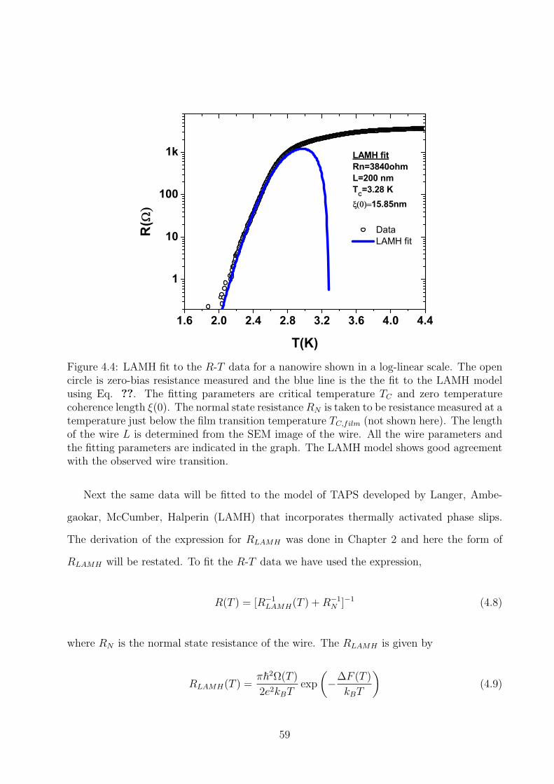
1.6 2.0 2.4 2.8 3.2 3.6 4.0 4.4
1
10
100
1k
Data LAMH fit
LAMH fitRn=3840ohmL=200 nmTC=3.28 K
15.85nm
R(
T(K)Figure 4.4: LAMH fit to the R-T data for a nanowire shown in a log-linear scale. The opencircle is zero-bias resistance measured and the blue line is the the fit to the LAMH modelusing Eq. ??. The fitting parameters are critical temperature TC and zero temperaturecoherence length ξ(0). The normal state resistance RN is taken to be resistance measured at atemperature just below the film transition temperature TC,film (not shown here). The lengthof the wire L is determined from the SEM image of the wire. All the wire parameters andthe fitting parameters are indicated in the graph. The LAMH model shows good agreementwith the observed wire transition.
Next the same data will be fitted to the model of TAPS developed by Langer, Ambe-
gaokar, McCumber, Halperin (LAMH) that incorporates thermally activated phase slips.
The derivation of the expression for RLAMH was done in Chapter 2 and here the form of
RLAMH will be restated. To fit the R-T data we have used the expression,
R(T ) = [R−1LAMH(T ) +R−1
N ]−1 (4.8)
where RN is the normal state resistance of the wire. The RLAMH is given by
RLAMH(T ) =π~
2Ω(T )
2e2kBTexp
(−∆F (T )
kBT
)(4.9)
59
where Ω(T ) is the attempt frequency given by,
Ω(T ) =
(L
ξ(T )
)√(∆F (T )
kBT
)(1
τGL
)(4.10)
with τGL = [π~/8kB(TC − T )] is the GL relaxation time. The form of ∆F (T ) is the same as
used for Little’s fit (Eq. 4.7).
To do the fit the fitting parameters are critical temperature TC and zero temperature
coherence length ξ(0). The normal state resistance RN is taken to be resistance measured at a
temperature just below the film transition temperature TC,film (not shown here). The length
of the wire L is determined from the SEM image of the wire. A fitting to the measured R-T
data (as used in Little fit in Fig. 4.3) is shown for the wire of L = 200 nm and RN = 3840 Ω
in Fig. 4.4. All the wire parameters and the fitting parameters are indicated in the graph.
It is found that the LAMH model can efficiently explain the wire transition.
Its found that both the Little and LAMH model explain the resistive transition of the
wire very well. But the fitting parameters TC and ξ(0) for both the fits are slightly different.
Nevertheless, the resistive transition captured in the zero-bias measurement of wires are
explained by thermally activated phase slips (TAPS). There is no evidence of quantum
phase slips in these measurements.
60
Chapter 5
Switching current measurements of
superconducting nanowires
5.1 High-bias V (I) measurements
A representative set of voltage-current characteristics V (I), measured at various tempera-
tures, is shown in Fig.5.1. These data show that, as the bias current is swept from low to
high, the system exhibits an abrupt transition from a zero or extremely low-voltage state
(i.e., a superconducting state) to a high-voltage state (i.e., a normal state) in which the
resistance is close to RN (22). We call the current at which switching occurs the switching
current ISW . Similarly, as the bias current is swept from high to low, the state reverts to
being superconducting, doing so at a retrapping current IR. We indicate these currents in
Fig. 5.1 for data taken at 0.3 K. As can be seen from Fig. 5.1, our nanowires are strongly
hysteretic: there is a regime of currents within which the wire is bistable (i.e., two voltage
states, one superconductive and one normal, are locally stable), and one of the two states is
realized depending upon the current history.
We find that the switching current of a nanowire ISW increases with decrease in the tem-
perature while the retrapping current IR increases by a very small amount as the temperature
is decreased. This essentially leads to the increase of the hysteresis as the temperature is
decreased (as shown Fig. 5.1). At high temperatures when the wire is in a normal state the
V (I) curves of a nanowire is linear or ohmic in nature without any hysteresis loop. Also at
high temperatures, we see voltage “tails”before the the wire switches to the normal state.
This is shown in the V -I curves shown in Fig. 5.2. These voltage tails appear due to many
phase slips occurring in the wire before it switches to the resistive state with a resistance
61
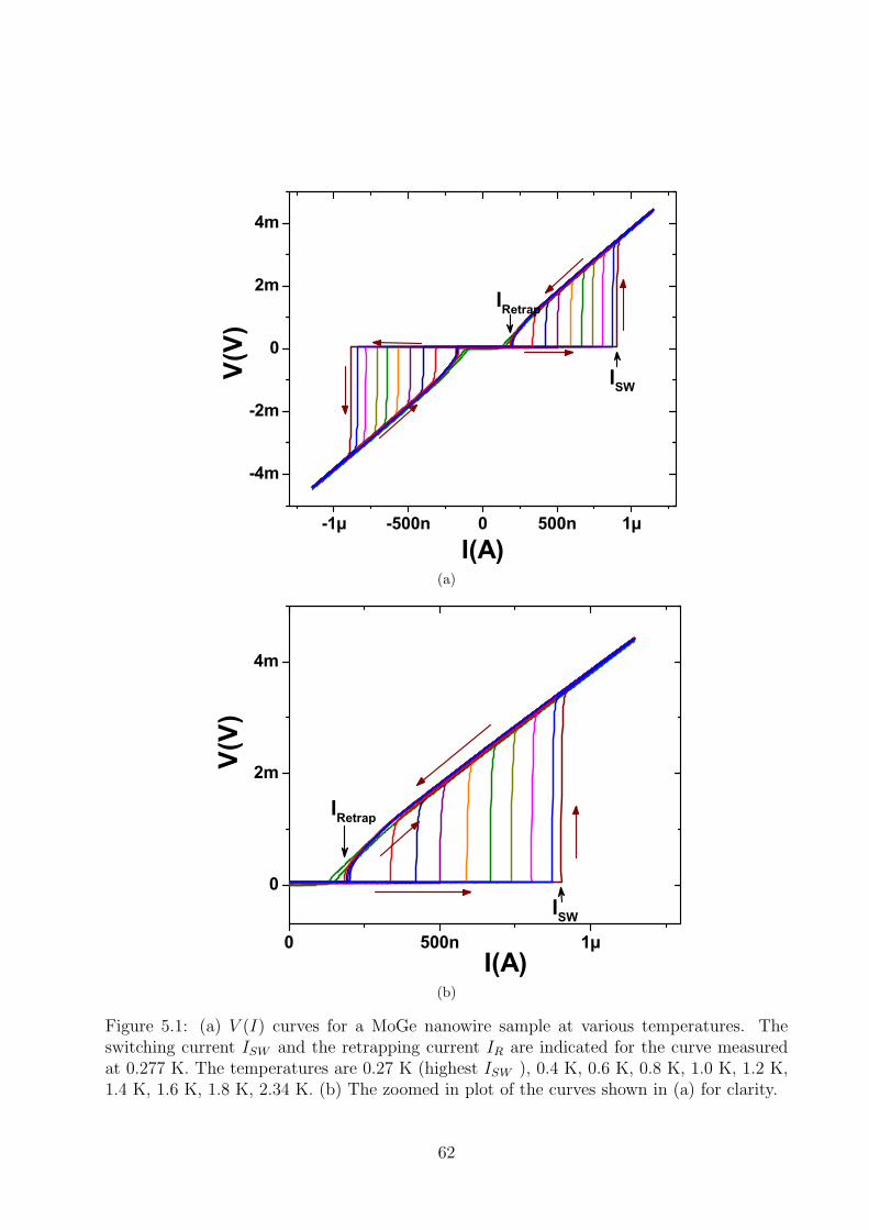
-1µ -500n 0 500n 1µ
-4m
-2m
0
2m
4m
IRetrap
V(V)
I(A)
ISW
(a)
0 500n 1µ
0
2m
4m
IRetrap
V(V)
I(A)
ISW
(b)
Figure 5.1: (a) V (I) curves for a MoGe nanowire sample at various temperatures. Theswitching current ISW and the retrapping current IR are indicated for the curve measuredat 0.277 K. The temperatures are 0.27 K (highest ISW ), 0.4 K, 0.6 K, 0.8 K, 1.0 K, 1.2 K,1.4 K, 1.6 K, 1.8 K, 2.34 K. (b) The zoomed in plot of the curves shown in (a) for clarity.
62
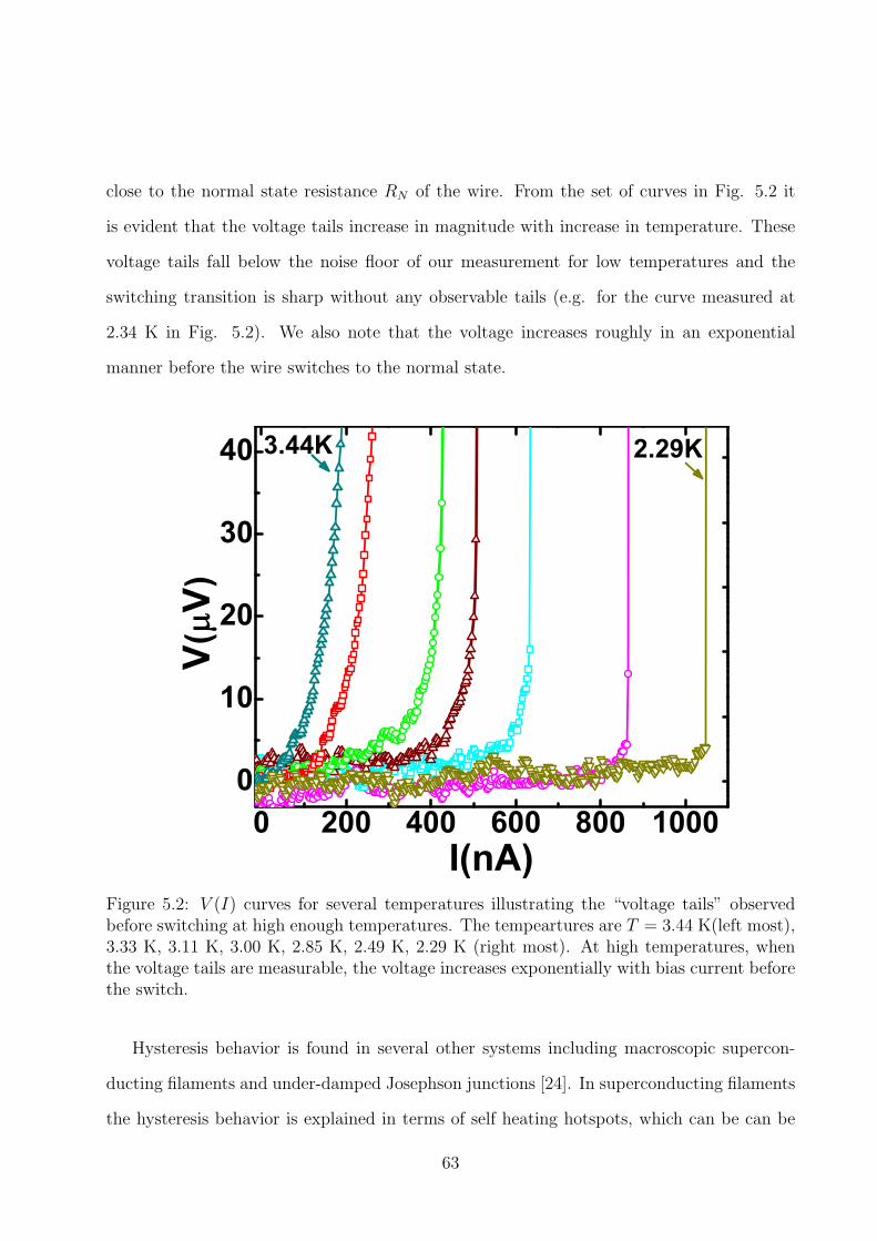
close to the normal state resistance RN of the wire. From the set of curves in Fig. 5.2 it
is evident that the voltage tails increase in magnitude with increase in temperature. These
voltage tails fall below the noise floor of our measurement for low temperatures and the
switching transition is sharp without any observable tails (e.g. for the curve measured at
2.34 K in Fig. 5.2). We also note that the voltage increases roughly in an exponential
manner before the wire switches to the normal state.
0 200 400 600 800 10000
10
20
30
40 2.29K
V(V)
I(nA)
3.44K
Figure 5.2: V (I) curves for several temperatures illustrating the “voltage tails” observedbefore switching at high enough temperatures. The tempeartures are T = 3.44 K(left most),3.33 K, 3.11 K, 3.00 K, 2.85 K, 2.49 K, 2.29 K (right most). At high temperatures, whenthe voltage tails are measurable, the voltage increases exponentially with bias current beforethe switch.
Hysteresis behavior is found in several other systems including macroscopic supercon-
ducting filaments and under-damped Josephson junctions [24]. In superconducting filaments
the hysteresis behavior is explained in terms of self heating hotspots, which can be can be
63
used as the basis for the hot-electron bolometers [54].In under-damped Josephson junction
system the hysteresis is attributed to the run-away and retrapping of the phase particle in
the tilted washboard potential of the Josephson junction without considering any heating
effect [30]. Our wires show hysteresis even though they are overdamped and many phase
slips occur at high temperatures before the wire switches to the normal state. Tinkham and
co-workers [54] have considered the effect of phase slip in heating the wire. They showed that
the heat released during a phase slip process is not instantaneously dissipated but, rather
leads to alterations in local temperature of the quasi-one-dimensional system and resulting
flow of heat, which feed back to influence the phase slip kinetics. This feedback leads to
a switching bistability of the system involving a pair of mesoscopic states. One of these
states is essentially superconducting, low-voltage state and the other one is a more highly
resistive, high-voltage state. The rarity of the phase slips in the essentially superconducting
state mean that very little Joule heating takes place, which favors the persistence of the
state. However, the energy liberated by concentrated bursts of phase slips can Joule-heat
the system enough to weaken the superconductivity, and, via this feedback loop, lead to
the essential destruction of the superconductivity and the maintenance of the more strongly
Joule-heated, more highly resistive state.
5.2 Stochasticity of switching currents
We observe that even if the bath temperature T and the bias-current sweep protocol is kept
the same the measured switching current ISW varies from run to run. On the other hand, the
retrapping current IR is reproduced accurately within the experimental resolution . Hence,
the the switching current is statistically distributed and does not have a sharp value. This a
reflection of the collective dynamics of the superconducting condensate in the nanowire. The
condensate can be visualized as a fluctuating entity, evolving stochastically in time and, at
random instants undergoing phase slip events. the goal of this thesis work is to understand
64
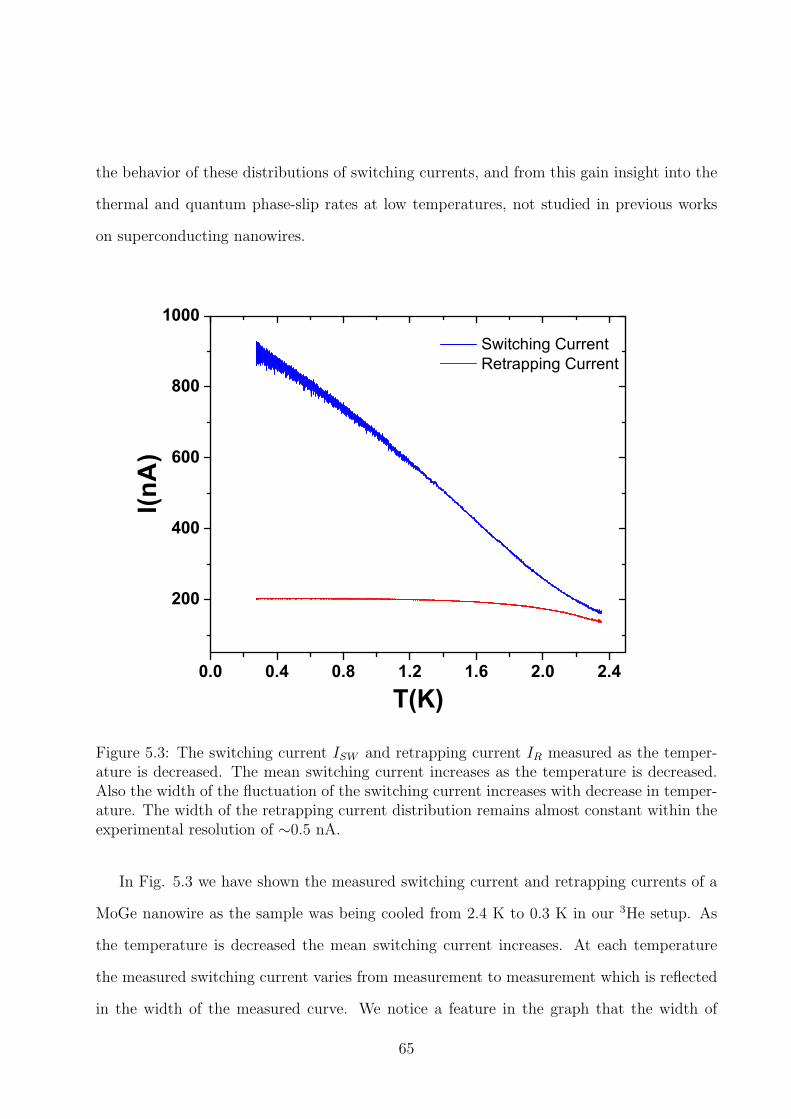
the behavior of these distributions of switching currents, and from this gain insight into the
thermal and quantum phase-slip rates at low temperatures, not studied in previous works
on superconducting nanowires.
0.0 0.4 0.8 1.2 1.6 2.0 2.4
200
400
600
800
1000 Switching Current Retrapping Current
I(nA)
T(K)
Figure 5.3: The switching current ISW and retrapping current IR measured as the temper-ature is decreased. The mean switching current increases as the temperature is decreased.Also the width of the fluctuation of the switching current increases with decrease in temper-ature. The width of the retrapping current distribution remains almost constant within theexperimental resolution of ∼0.5 nA.
In Fig. 5.3 we have shown the measured switching current and retrapping currents of a
MoGe nanowire as the sample was being cooled from 2.4 K to 0.3 K in our 3He setup. As
the temperature is decreased the mean switching current increases. At each temperature
the measured switching current varies from measurement to measurement which is reflected
in the width of the measured curve. We notice a feature in the graph that the width of
65
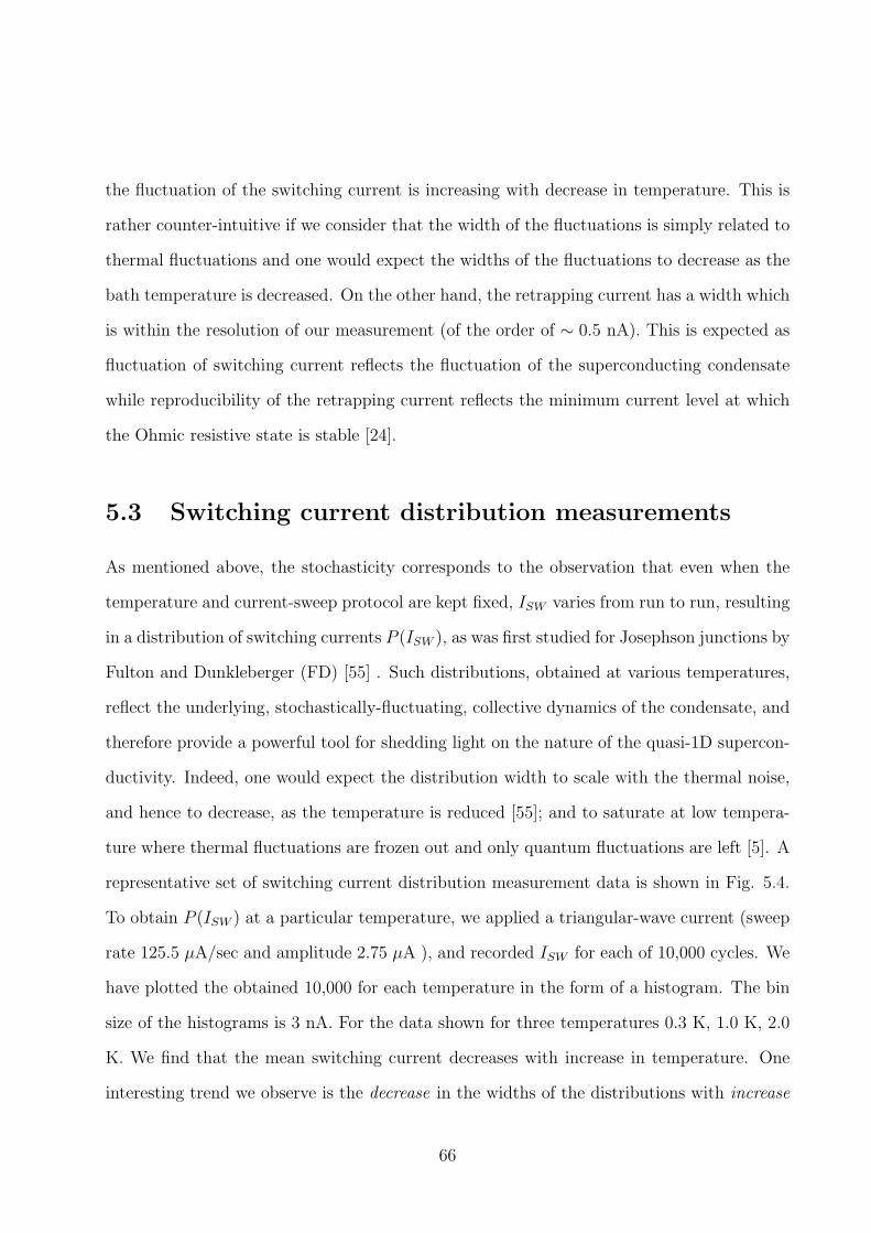
the fluctuation of the switching current is increasing with decrease in temperature. This is
rather counter-intuitive if we consider that the width of the fluctuations is simply related to
thermal fluctuations and one would expect the widths of the fluctuations to decrease as the
bath temperature is decreased. On the other hand, the retrapping current has a width which
is within the resolution of our measurement (of the order of ∼ 0.5 nA). This is expected as
fluctuation of switching current reflects the fluctuation of the superconducting condensate
while reproducibility of the retrapping current reflects the minimum current level at which
the Ohmic resistive state is stable [24].
5.3 Switching current distribution measurements
As mentioned above, the stochasticity corresponds to the observation that even when the
temperature and current-sweep protocol are kept fixed, ISW varies from run to run, resulting
in a distribution of switching currents P (ISW ), as was first studied for Josephson junctions by
Fulton and Dunkleberger (FD) [55] . Such distributions, obtained at various temperatures,
reflect the underlying, stochastically-fluctuating, collective dynamics of the condensate, and
therefore provide a powerful tool for shedding light on the nature of the quasi-1D supercon-
ductivity. Indeed, one would expect the distribution width to scale with the thermal noise,
and hence to decrease, as the temperature is reduced [55]; and to saturate at low tempera-
ture where thermal fluctuations are frozen out and only quantum fluctuations are left [5]. A
representative set of switching current distribution measurement data is shown in Fig. 5.4.
To obtain P (ISW ) at a particular temperature, we applied a triangular-wave current (sweep
rate 125.5 µA/sec and amplitude 2.75 µA ), and recorded ISW for each of 10,000 cycles. We
have plotted the obtained 10,000 for each temperature in the form of a histogram. The bin
size of the histograms is 3 nA. For the data shown for three temperatures 0.3 K, 1.0 K, 2.0
K. We find that the mean switching current decreases with increase in temperature. One
interesting trend we observe is the decrease in the widths of the distributions with increase
66
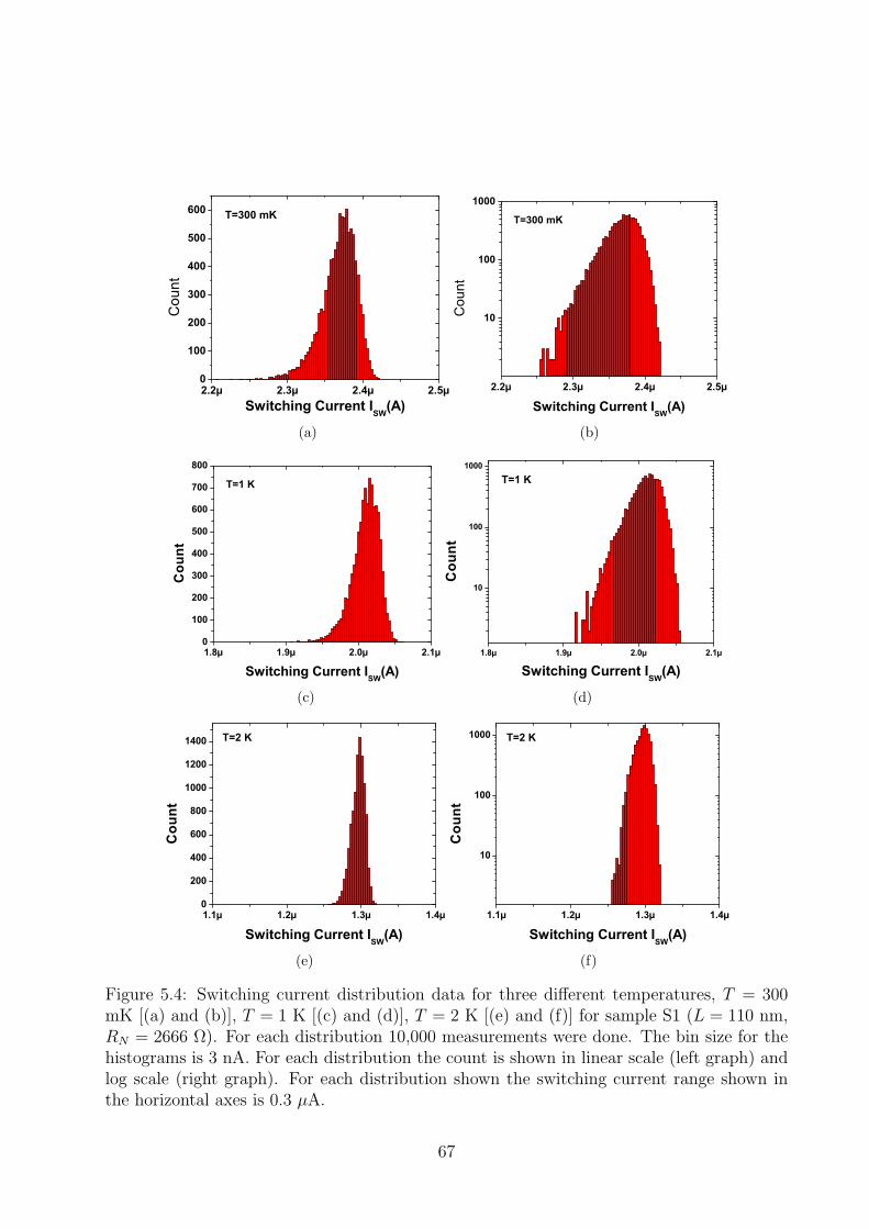
2.2µ 2.3µ 2.4µ 2.5µ0
100
200
300
400
500
600
C
ount
Switching Current ISW(A)
T=300 mK
(a)
2.2µ 2.3µ 2.4µ 2.5µ
10
100
1000
Cou
nt
Switching Current ISW(A)
T=300 mK
(b)
1.8µ 1.9µ 2.0µ 2.1µ0
100
200
300
400
500
600
700
800
Cou
nt
Switching Current ISW(A)
T=1 K
(c)
1.8µ 1.9µ 2.0µ 2.1µ
10
100
1000
Cou
nt
Switching Current ISW(A)
T=1 K
(d)
1.1µ 1.2µ 1.3µ 1.4µ0
200
400
600
800
1000
1200
1400
Cou
nt
Switching Current ISW(A)
T=2 K
(e)
1.1µ 1.2µ 1.3µ 1.4µ
10
100
1000
Cou
nt
Switching Current ISW(A)
T=2 K
(f)
Figure 5.4: Switching current distribution data for three different temperatures, T = 300mK [(a) and (b)], T = 1 K [(c) and (d)], T = 2 K [(e) and (f)] for sample S1 (L = 110 nm,RN = 2666 Ω). For each distribution 10,000 measurements were done. The bin size for thehistograms is 3 nA. For each distribution the count is shown in linear scale (left graph) andlog scale (right graph). For each distribution shown the switching current range shown inthe horizontal axes is 0.3 µA.
67
1.0 1.2 1.4 1.6 1.8 2.0 2.2 2.40
2k
0.3K
Cou
nt
2.3K
Switching Current, ISW( A)Figure 5.5: Switching current distributions P (ISW ) for 21 temperatures between 0.3 K (rightmost) and 2.3 K (left most) with ∆T = 0.1 K for sample S1 (L = 110 nm, RN = 2666 Ω). Foreach distribution 10,000 switching events were recorded and the bin size of the histogramsis 3 nA.
68
in temperature (as indicated from the data shown in Fig. 5.3). We would like to mention
that this observed trend is exact opposite to what was observed by Fulton and Dunkleberger
[55] on their measurements on Sn–Sn-oxide–Sn junctions. They found the widths of the
distributions to increase with increase in temperatures.
The switching current distributions at 21 temperatures from 0.3 K to 2.3 K with a
temperature interval of ∆T = 0.1 K is shown in Fig. 5.5. A total 10,000 number of mea-
surements were done for each distribution shown. The bin size of each histogram is 3 nA.
As the temperature is decreased the height of the distribution is decreasing and the width
is increasing. We repeated similar switching current distribution measurements for several
nanowire samples. Here we are showing the data for another four MoGe nanowire samples
(total 5 nanowires). In Fig. 5.6, the switching current distributions are shown for measure-
ments between 0.3 K and 1.8 K with a temperature interval of ∆T = 0.1 K for wire S2
(L = 195 nm, RN = 4100 Ω). In Fig. 5.7, the switching current distributions are shown for
measurements between 0.3 K and 1.4 K with a temperature interval of ∆T = 0.1 K for wire
S3 (L = 104 nm, RN = 1430 Ω). In Fig. 5.8, the switching current distributions are shown
for measurements between 0.277 K and 1.6 K for wire S4 (L = 200 nm, RN = 3900 Ω). The
bath temperature for each distribution is indicated in the graph.
69
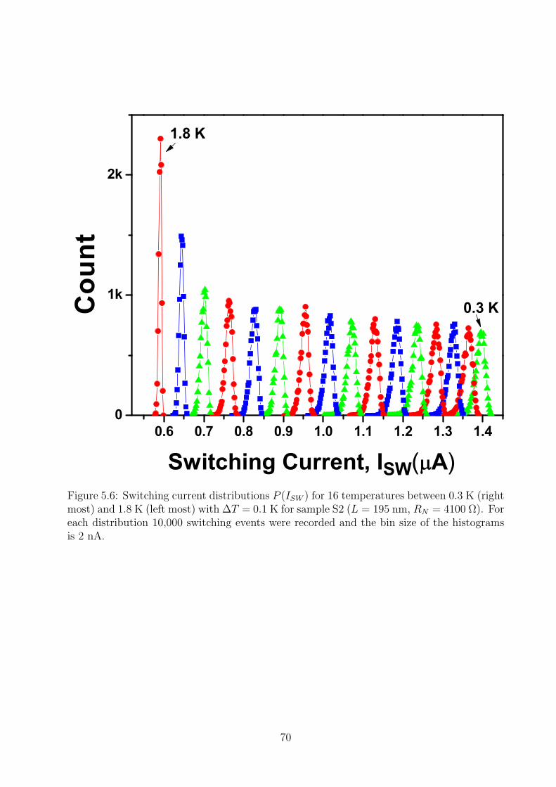
0.6 0.7 0.8 0.9 1.0 1.1 1.2 1.3 1.40
1k
2k
1.8 K
Cou
nt
0.3 K
Switching Current, ISW( A)Figure 5.6: Switching current distributions P (ISW ) for 16 temperatures between 0.3 K (rightmost) and 1.8 K (left most) with ∆T = 0.1 K for sample S2 (L = 195 nm, RN = 4100 Ω). Foreach distribution 10,000 switching events were recorded and the bin size of the histogramsis 2 nA.
70
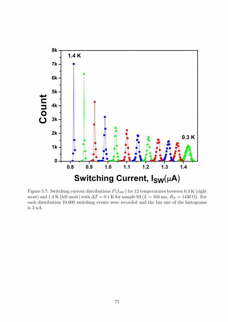
0.8 0.9 1.0 1.1 1.2 1.3 1.40
1k
2k
3k
4k
5k
6k
7k
8k
0.3 K
Cou
nt1.4 K
Switching Current, ISW( A)Figure 5.7: Switching current distributions P (ISW ) for 12 temperatures between 0.3 K (rightmost) and 1.4 K (left most) with ∆T = 0.1 K for sample S3 (L = 104 nm, RN = 1430 Ω). Foreach distribution 10,000 switching events were recorded and the bin size of the histogramsis 3 nA.
71
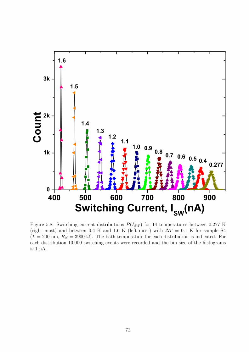
400 500 600 700 800 9000
1k
2k
3k
1.6
1.5
0.277
1.41.3
0.6 0.5 0.40.70.80.91.0
1.11.2
Cou
nt
Switching Current, ISW(nA)Figure 5.8: Switching current distributions P (ISW ) for 14 temperatures between 0.277 K(right most) and between 0.4 K and 1.6 K (left most) with ∆T = 0.1 K for sample S4(L = 200 nm, RN = 3900 Ω). The bath temperature for each distribution is indicated. Foreach distribution 10,000 switching events were recorded and the bin size of the histogramsis 1 nA.
72
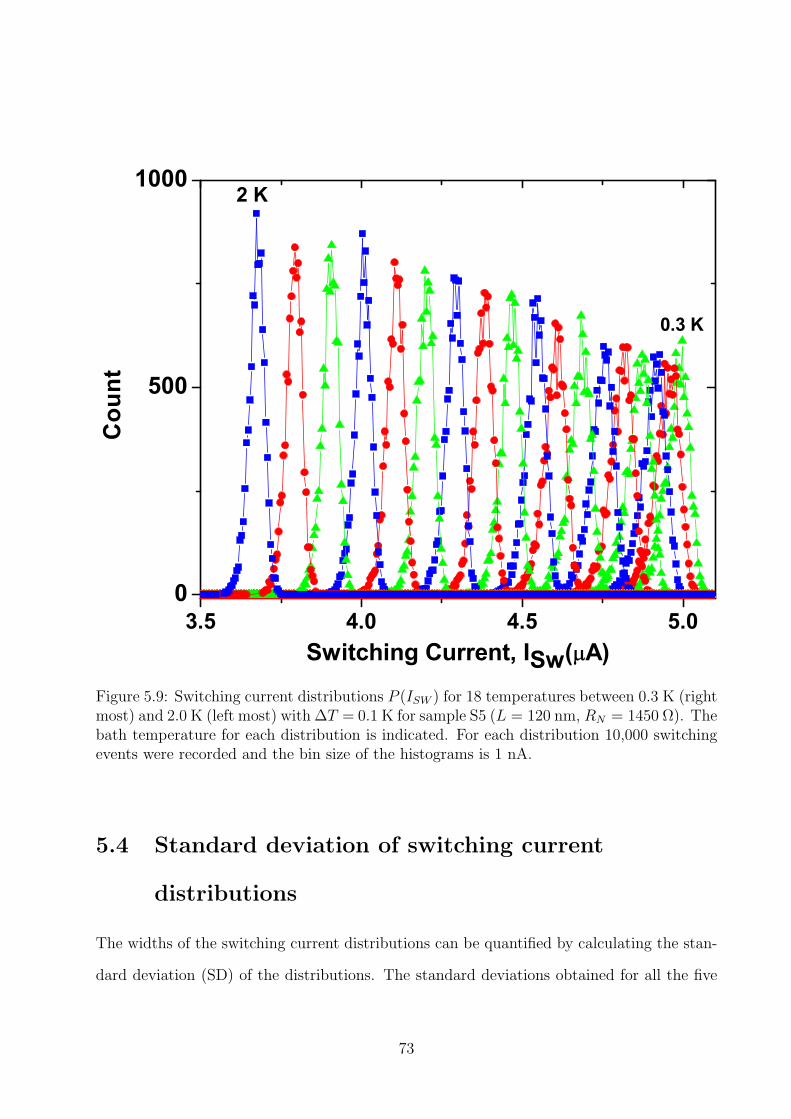
3.5 4.0 4.5 5.00
500
1000
Cou
nt
Switching Current, ISw( A)
2 K
0.3 K
Figure 5.9: Switching current distributions P (ISW ) for 18 temperatures between 0.3 K (rightmost) and 2.0 K (left most) with ∆T = 0.1 K for sample S5 (L = 120 nm, RN = 1450 Ω). Thebath temperature for each distribution is indicated. For each distribution 10,000 switchingevents were recorded and the bin size of the histograms is 1 nA.
5.4 Standard deviation of switching current
distributions
The widths of the switching current distributions can be quantified by calculating the stan-
dard deviation (SD) of the distributions. The standard deviations obtained for all the five
73
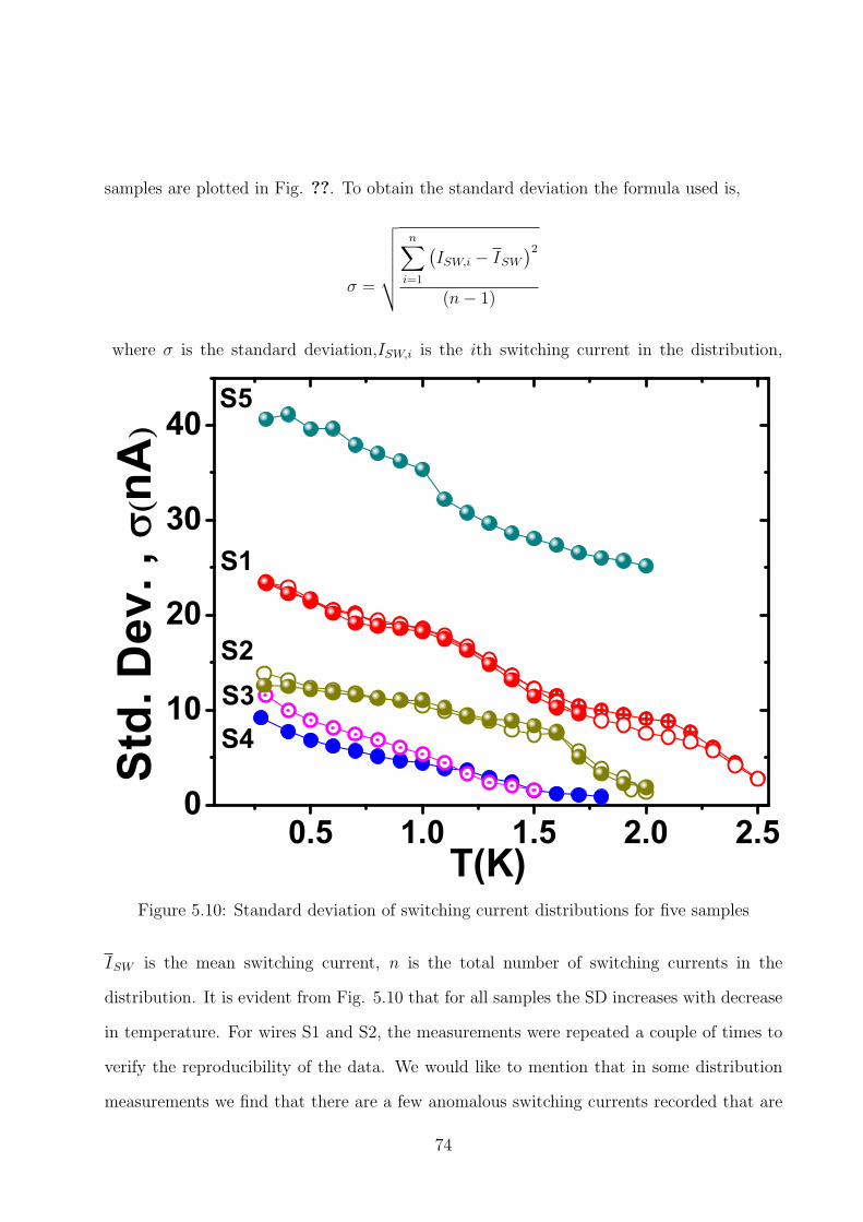
samples are plotted in Fig. ??. To obtain the standard deviation the formula used is,
σ =
√√√√√√
n∑
i=1
(ISW,i − ISW
)2
(n− 1)
where σ is the standard deviation,ISW,i is the ith switching current in the distribution,
0.5 1.0 1.5 2.0 2.50
10
20
30
40S5
S4S3S2
Std
. Dev
. ,
nA
T(K)
S1
Figure 5.10: Standard deviation of switching current distributions for five samples
ISW is the mean switching current, n is the total number of switching currents in the
distribution. It is evident from Fig. 5.10 that for all samples the SD increases with decrease
in temperature. For wires S1 and S2, the measurements were repeated a couple of times to
verify the reproducibility of the data. We would like to mention that in some distribution
measurements we find that there are a few anomalous switching currents recorded that are
74
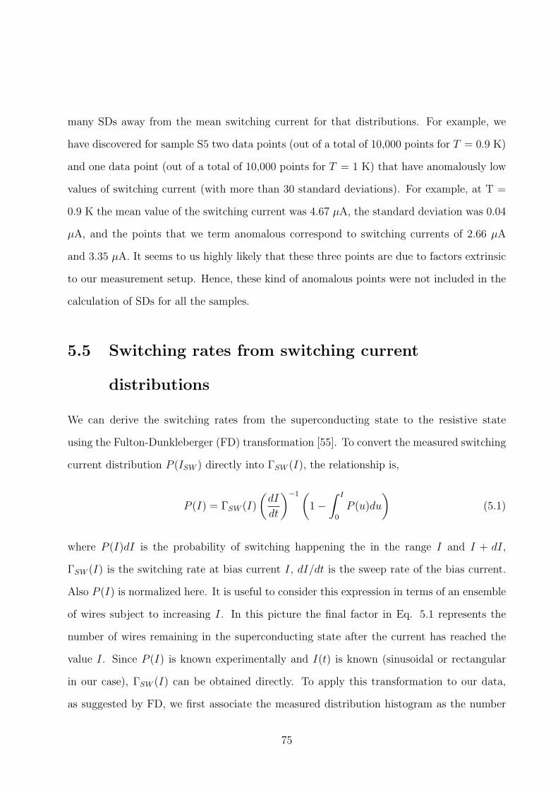
many SDs away from the mean switching current for that distributions. For example, we
have discovered for sample S5 two data points (out of a total of 10,000 points for T = 0.9 K)
and one data point (out of a total of 10,000 points for T = 1 K) that have anomalously low
values of switching current (with more than 30 standard deviations). For example, at T =
0.9 K the mean value of the switching current was 4.67 µA, the standard deviation was 0.04
µA, and the points that we term anomalous correspond to switching currents of 2.66 µA
and 3.35 µA. It seems to us highly likely that these three points are due to factors extrinsic
to our measurement setup. Hence, these kind of anomalous points were not included in the
calculation of SDs for all the samples.
5.5 Switching rates from switching current
distributions
We can derive the switching rates from the superconducting state to the resistive state
using the Fulton-Dunkleberger (FD) transformation [55]. To convert the measured switching
current distribution P (ISW ) directly into ΓSW (I), the relationship is,
P (I) = ΓSW (I)
(dI
dt
)−1(1 −
∫ I
0
P (u)du
)(5.1)
where P (I)dI is the probability of switching happening the in the range I and I + dI,
ΓSW (I) is the switching rate at bias current I, dI/dt is the sweep rate of the bias current.
Also P (I) is normalized here. It is useful to consider this expression in terms of an ensemble
of wires subject to increasing I. In this picture the final factor in Eq. 5.1 represents the
number of wires remaining in the superconducting state after the current has reached the
value I. Since P (I) is known experimentally and I(t) is known (sinusoidal or rectangular
in our case), ΓSW (I) can be obtained directly. To apply this transformation to our data,
as suggested by FD, we first associate the measured distribution histogram as the number
75
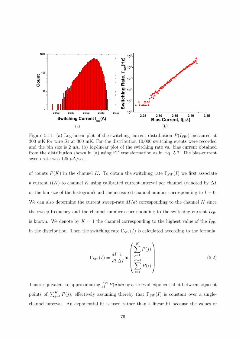
2.25µ 2.30µ 2.35µ 2.40µ 2.45µ1
10
100
1000
Cou
nt
Switching Current ISW(A)
(a)
2.25 2.30 2.35 2.40 2.45100
101
102
103
104
105
Switc
hing
Rat
e,
SW
(Hz)
Bias Current, I( )(b)
Figure 5.11: (a) Log-linear plot of the switching current distribution P (ISW ) measured at300 mK for wire S1 at 300 mK. For the distribution 10,000 switching events were recordedand the bin size is 2 nA. (b) log-linear plot of the switching rate vs. bias current obtainedfrom the distribution shown in (a) using FD transformation as in Eq. 5.2. The bias-currentsweep rate was 125 µA/sec.
of counts P (K) in the channel K. To obtain the switching rate ΓSW (I) we first associate
a current I(K) to channel K using calibrated current interval per channel (denoted by ∆I
or the bin size of the histogram) and the measured channel number corresponding to I = 0.
We can also determine the current sweep-rate dI/dt corresponding to the channel K since
the sweep frequency and the channel numbers corresponding to the switching current ISW
is known. We denote by K = 1 the channel corresponding to the highest value of the ISW
in the distribution. Then the switching rate ΓSW (I) is calculated according to the formula,
ΓSW (I) =dI
dt
1
∆Iln
K∑
j=1
P (j)
K−1∑
i=1
P (i)
(5.2)
This is equivalent to approximating∫∞
IP (u)du by a series of exponential fit between adjacent
points of∑K
j=1 P (j), effectively assuming thereby that ΓSW (I) is constant over a single-
channel interval. An exponential fit is used rather than a linear fit because the values of
76
P (K) may decreases quite abruptly for low values of K. Finally, ΓSW (K) is assigned to
I(K) to yield ΓSW (I).
An example of distribution to rate conversion using the FD method just described is
shown in Fig. 5.11. In Fig. 5.11a we have shown a log-linear plot of the switching current
distribution P (ISW ) measured at 300 mK for sample S1. To obtain To P (ISW ) at a particular
temperature, we applied a triangular-wave current (sweep rate dI/dt = 125.5 µA/sec and
amplitude 2.75 µA ), and recorded ISW for each of 10,000 cycles. The bin size of the
histogram is 2 nA. To get the switching rates from distribution measurement we used Eq.
5.2 with the known dI/dt and ∆I = 2 nA. The obtained switching rate vs. bias current
data is shown in Fig. 5.11b. We find our measurements the switching rates obtained are in
the range 1 − 105 Hz.
The switching rate data for sample S1 obtained at 21 equally spaced temperatures be-
tween 0.3 K and 2.3 K is shown in Fig. 5.16. The distribution data used for these rates are
shown in Fig. 5.5 before.
1.0µ 1.2µ 1.4µ 1.6µ 1.8µ 2.0µ 2.2µ 2.4µ100
101
102
103
104
105
Switc
hing
Rat
e,
SW(H
z)
Bias Current, ISW(A)
Figure 5.12: Switching rates obtained using FD transformation for wire S1 using the switch-ing current distributions in Fig. 5.5 for 21 equally spaced temperatures between 2.3 K (leftmost) and 0.3 K (right most).
77
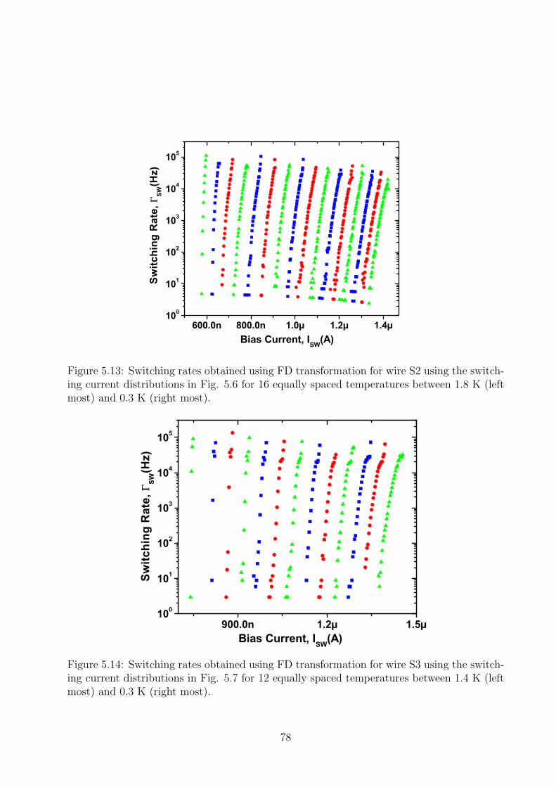
600.0n 800.0n 1.0µ 1.2µ 1.4µ100
101
102
103
104
105
Bias Current, ISW(A)
Switc
hing
Rat
e,
SW(H
z)
Figure 5.13: Switching rates obtained using FD transformation for wire S2 using the switch-ing current distributions in Fig. 5.6 for 16 equally spaced temperatures between 1.8 K (leftmost) and 0.3 K (right most).
900.0n 1.2µ 1.5µ100
101
102
103
104
105
Switc
hing
Rat
e,
SW(H
z)
Bias Current, ISW(A)
Figure 5.14: Switching rates obtained using FD transformation for wire S3 using the switch-ing current distributions in Fig. 5.7 for 12 equally spaced temperatures between 1.4 K (leftmost) and 0.3 K (right most).
78
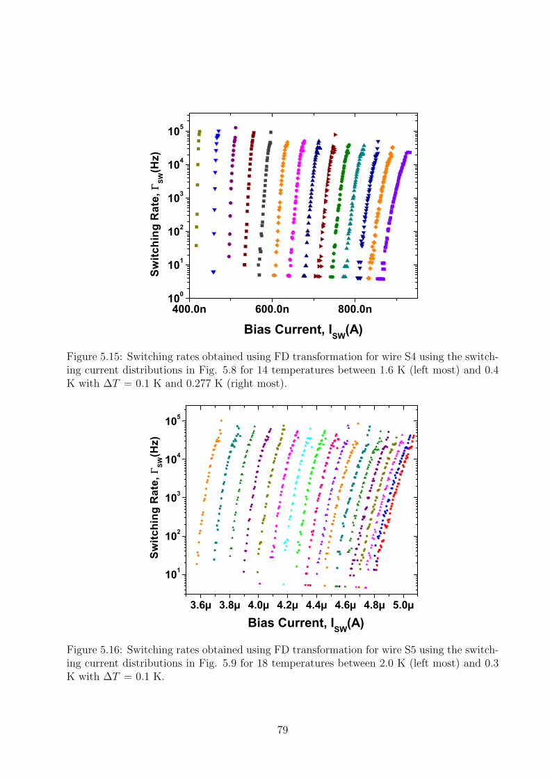
400.0n 600.0n 800.0n100
101
102
103
104
105
Switc
hing
Rat
e,
SW(H
z)
Bias Current, ISW(A)
Figure 5.15: Switching rates obtained using FD transformation for wire S4 using the switch-ing current distributions in Fig. 5.8 for 14 temperatures between 1.6 K (left most) and 0.4K with ∆T = 0.1 K and 0.277 K (right most).
3.6µ 3.8µ 4.0µ 4.2µ 4.4µ 4.6µ 4.8µ 5.0µ
101
102
103
104
105
Switc
hing
Rat
e,
SW(H
z)
Bias Current, ISW(A)
Figure 5.16: Switching rates obtained using FD transformation for wire S5 using the switch-ing current distributions in Fig. 5.9 for 18 temperatures between 2.0 K (left most) and 0.3K with ∆T = 0.1 K.
79
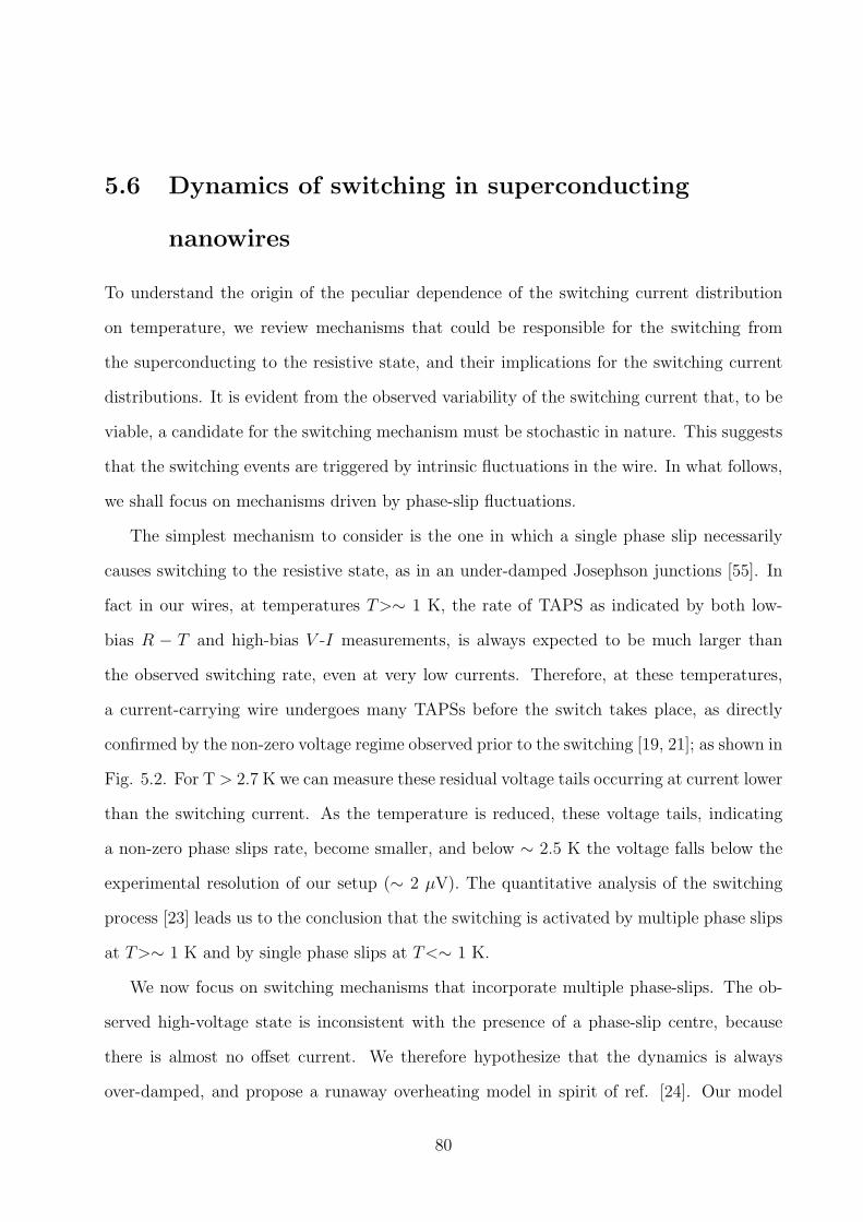
5.6 Dynamics of switching in superconducting
nanowires
To understand the origin of the peculiar dependence of the switching current distribution
on temperature, we review mechanisms that could be responsible for the switching from
the superconducting to the resistive state, and their implications for the switching current
distributions. It is evident from the observed variability of the switching current that, to be
viable, a candidate for the switching mechanism must be stochastic in nature. This suggests
that the switching events are triggered by intrinsic fluctuations in the wire. In what follows,
we shall focus on mechanisms driven by phase-slip fluctuations.
The simplest mechanism to consider is the one in which a single phase slip necessarily
causes switching to the resistive state, as in an under-damped Josephson junctions [55]. In
fact in our wires, at temperatures T>∼ 1 K, the rate of TAPS as indicated by both low-
bias R − T and high-bias V -I measurements, is always expected to be much larger than
the observed switching rate, even at very low currents. Therefore, at these temperatures,
a current-carrying wire undergoes many TAPSs before the switch takes place, as directly
confirmed by the non-zero voltage regime observed prior to the switching [19, 21]; as shown in
Fig. 5.2. For T > 2.7 K we can measure these residual voltage tails occurring at current lower
than the switching current. As the temperature is reduced, these voltage tails, indicating
a non-zero phase slips rate, become smaller, and below ∼ 2.5 K the voltage falls below the
experimental resolution of our setup (∼ 2 µV). The quantitative analysis of the switching
process [23] leads us to the conclusion that the switching is activated by multiple phase slips
at T>∼ 1 K and by single phase slips at T<∼ 1 K.
We now focus on switching mechanisms that incorporate multiple phase-slips. The ob-
served high-voltage state is inconsistent with the presence of a phase-slip centre, because
there is almost no offset current. We therefore hypothesize that the dynamics is always
over-damped, and propose a runaway overheating model in spirit of ref. [24]. Our model
80
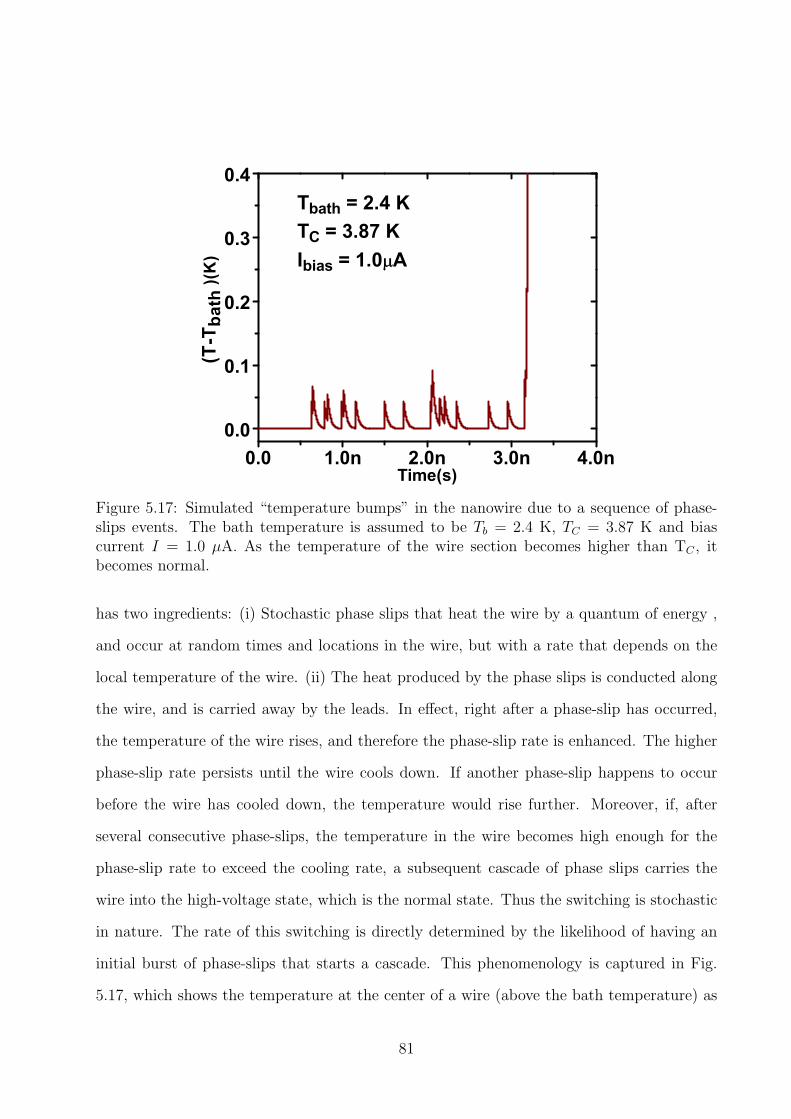
0.0 1.0n 2.0n 3.0n 4.0n0.0
0.1
0.2
0.3
0.4Tbath = 2.4 KTC = 3.87 KIbias = 1.0 A
(T-T
bath
)(K
)
Time(s)
Figure 5.17: Simulated “temperature bumps” in the nanowire due to a sequence of phase-slips events. The bath temperature is assumed to be Tb = 2.4 K, TC = 3.87 K and biascurrent I = 1.0 µA. As the temperature of the wire section becomes higher than TC , itbecomes normal.
has two ingredients: (i) Stochastic phase slips that heat the wire by a quantum of energy ,
and occur at random times and locations in the wire, but with a rate that depends on the
local temperature of the wire. (ii) The heat produced by the phase slips is conducted along
the wire, and is carried away by the leads. In effect, right after a phase-slip has occurred,
the temperature of the wire rises, and therefore the phase-slip rate is enhanced. The higher
phase-slip rate persists until the wire cools down. If another phase-slip happens to occur
before the wire has cooled down, the temperature would rise further. Moreover, if, after
several consecutive phase-slips, the temperature in the wire becomes high enough for the
phase-slip rate to exceed the cooling rate, a subsequent cascade of phase slips carries the
wire into the high-voltage state, which is the normal state. Thus the switching is stochastic
in nature. The rate of this switching is directly determined by the likelihood of having an
initial burst of phase-slips that starts a cascade. This phenomenology is captured in Fig.
5.17, which shows the temperature at the center of a wire (above the bath temperature) as
81
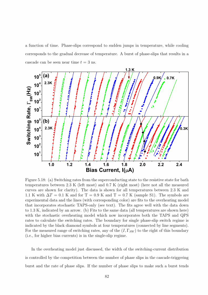
a function of time. Phase-slips correspond to sudden jumps in temperature, while cooling
corresponds to the gradual decrease of temperature. A burst of phase-slips that results in a
cascade can be seen near time t = 3 ns.
1.0 1.2 1.4 1.6 1.8 2.0 2.2 2.4
101
102
103
104
105 (b)2.3K
101
102
103
104
1050.9K 0.7K
0.3K
Bias Current, I( A)
Switc
hing
Rat
e,
SW(H
z)
2.3K
1.3 K(a)
Figure 5.18: (a) Switching rates from the superconducting state to the resistive state for bathtemperatures between 2.3 K (left most) and 0.7 K (right most) (here not all the measuredcurves are shown for clarity). The data is shown for all temperatures between 2.3 K and1.1 K with ∆T = 0.1 K and for T = 0.9 K and T = 0.7 K (sample S1). The symbols areexperimental data and the lines (with corresponding color) are fits to the overheating modelthat incorporates stochastic TAPS-only (see text). The fits agree well with the data downto 1.3 K, indicated by an arrow. (b) Fits to the same data (all temperatures are shown here)with the stochastic overheating model which now incorporates both the TAPS and QPSrates to calculate the switching rates. The boundary for single phase-slip switch regime isindicated by the black diamond symbols at four temperatures (connected by line segments).For the measured range of switching rates, any of the (I,ΓSW ) to the right of this boundary(i.e., for higher bias currents) is in the single-slip regime.
In the overheating model just discussed, the width of the switching-current distribution
is controlled by the competition between the number of phase slips in the cascade-triggering
burst and the rate of phase slips. If the number of phase slips to make such a burst tends
82
to unity, the switching rate approaches the phase-slip rate. In the opposite regime, in which
a large number of phase-slips are required to form the burst, the switching rate is much
lower than the phase-slip rate. At higher temperatures, many phase slips are needed in
the initial burst, and thus switching tends to occur only when ISW is in a very narrow
range close to IC , thus making the distribution narrow. As the temperature decreases, the
heat capacity and heat conductivity both decrease, making phase-slips more effective at
heating the wire. Thus, the typical number of phase slips in the cascade-triggering burst
decreases with temperature, as our model shows [23]. At the same time, the rate of TAPS
also decreases with temperature. In practice, with decreasing temperature, the broadening
effect of the burst length on PSW (I) overwhelms the narrowing effect of the decreasing TAPS
rate, and this provides a possible explanation of the unanticipated broadening of the ISW
distributions.
We first tried to fit all the switching-rate data in Fig. 5.18 using the overheating model
but with a phase-slip rate Γ that follows from allowing only thermally-activated (and not
quantum) processes, i.e., ΓTAPS. At temperature T and bias-current I, ΓTAPS is given by,
ΓTAPS =ΩTAPS(T )
2πexp
(−∆F (T, I)
kBT
)(5.3)
where ΩTAPS(T ) is the attempt frequency, ∆F (T, I) = ∆F (T )(1 −
(I
IC(T )
))5/4
is the free-
energy barrier at bias-current I [25, 24],IC(T ) is the fluctuation-free depairing current, and
∆F (T ) =√
6~IC(T )2e
is the free-energy barrier at zero bias-current. These fits agree well with
the data over the temperature range 2.4 K to 1.3 K (Fig. 5.18b). Within this range, we
can attribute the decrease in the width of the distribution to the mechanism described in
the previous paragraph: the competition between (i) the number of phase slips in the initial
burst required to start a cascade, and (ii) the rate of phase slips. However, below 1.2 K it is
evident from Fig. 3a that the switching rates predicted by TAPS are considerably smaller
than the switching rates obtained experimentally.
83
5.7 Quantum phase slip and single phase-slip regime
As the temperature is reduced and fluctuations become smaller, the switching happens at
higher values of the bias-current I. Thus each phase slip releases more heat into the wire
(Ih/2e). Also, as bias-current I is increased, the value of the temperature increase required
in order to reach the normal state becomes smaller. Therefore, according to the overheating
model one ultimately expects to have a low T regime in which a single phase-slip event
releases enough heat to induce a switching event [23]. We call this the single-slip regime.
We expect that for T < ∼ 0.7 K, the wire S1 should be operating in this single-slip regime,
as indicated in Fig. 5.18b (the black curve). We find, however, in the regime 0.3 K < T <
1.2 K our data can not be fitted well if the phase-slip rate is taken to be ΓTAPS, but can be
fitted well if the total phase-slip rate (ΓTOTAL) is taken to be the sum of TAPS rate (ΓTAPS)
and QPS rate (ΓQPS),i.e.,
ΓTOTAL = ΓTAPS + ΓQPS (5.4)
Since at 0.3 K we are already in the single-slip regime the switching rate should be equal
to the phase-slip rate. We now introduce a simple model of QPS that was suggested by
Giordano [35, 10]. We use this model, but instead of the Ginzburg-Landau relaxation time,
which is only correct near TC , we use the notion of the effective “quantum” temperature
TQPS, which is a common (and well-tested) approach in Josephson junctions (JJ) [5]. Thus,
the QPS rate is given by the same expression as the TAPS rate but with the wire temperature
T replaced by an effective “quantum” temperature TQPS(T ), i.e.,
ΓQPS =ΩQPS(T )
2πexp
(−∆F (T, I)
kBTQPS
)
=
(L
ξ(T )
)(1
τGL
)(∆F (T )
kBTQPS
)1/2
exp
(−∆F (T, I)
kBTQPS
)(5.5)
As shown in Fig. 5.19, at 0.3 K, the measured switching rate can be fitted by the
Giordano-type QPS rate. For T = 0.3 K, the switching rate predicted by TAPS is roughly
84
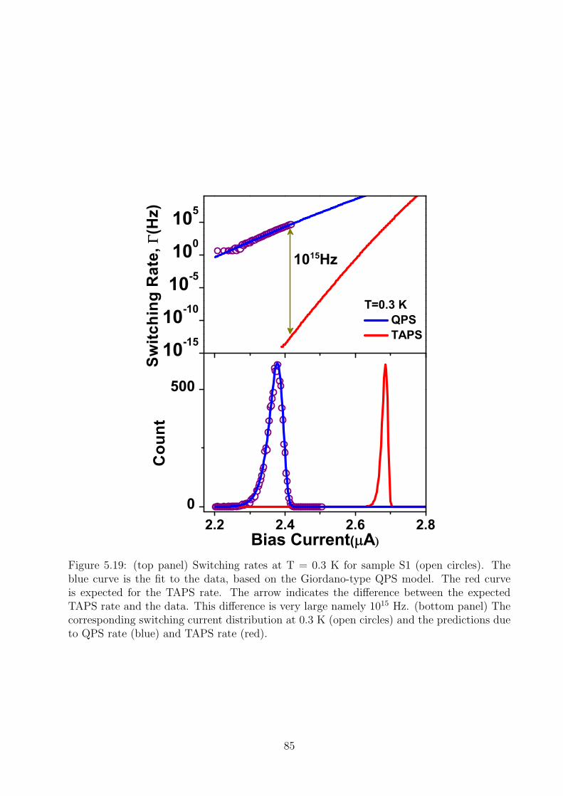
2.2 2.4 2.6 2.80
500
Bias Current( A
Cou
nt
10-15
10-10
10-5
100
105
T=0.3 K QPS TAPS
Switc
hing
Rat
e,
(Hz)
1015Hz
Figure 5.19: (top panel) Switching rates at T = 0.3 K for sample S1 (open circles). Theblue curve is the fit to the data, based on the Giordano-type QPS model. The red curveis expected for the TAPS rate. The arrow indicates the difference between the expectedTAPS rate and the data. This difference is very large namely 1015 Hz. (bottom panel) Thecorresponding switching current distribution at 0.3 K (open circles) and the predictions dueto QPS rate (blue) and TAPS rate (red).
85
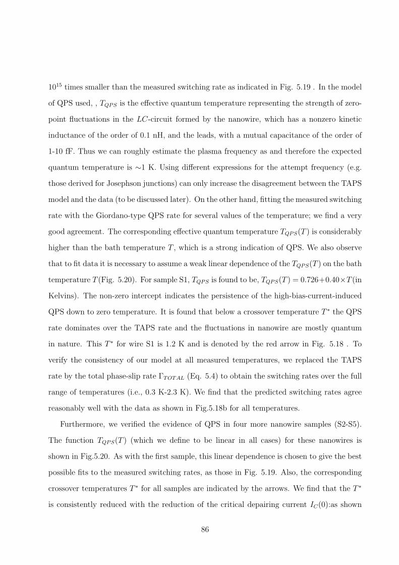
1015 times smaller than the measured switching rate as indicated in Fig. 5.19 . In the model
of QPS used, , TQPS is the effective quantum temperature representing the strength of zero-
point fluctuations in the LC-circuit formed by the nanowire, which has a nonzero kinetic
inductance of the order of 0.1 nH, and the leads, with a mutual capacitance of the order of
1-10 fF. Thus we can roughly estimate the plasma frequency as and therefore the expected
quantum temperature is ∼1 K. Using different expressions for the attempt frequency (e.g.
those derived for Josephson junctions) can only increase the disagreement between the TAPS
model and the data (to be discussed later). On the other hand, fitting the measured switching
rate with the Giordano-type QPS rate for several values of the temperature; we find a very
good agreement. The corresponding effective quantum temperature TQPS(T ) is considerably
higher than the bath temperature T , which is a strong indication of QPS. We also observe
that to fit data it is necessary to assume a weak linear dependence of the TQPS(T ) on the bath
temperature T (Fig. 5.20). For sample S1, TQPS is found to be, TQPS(T ) = 0.726+0.40×T (in
Kelvins). The non-zero intercept indicates the persistence of the high-bias-current-induced
QPS down to zero temperature. It is found that below a crossover temperature T ∗ the QPS
rate dominates over the TAPS rate and the fluctuations in nanowire are mostly quantum
in nature. This T ∗ for wire S1 is 1.2 K and is denoted by the red arrow in Fig. 5.18 . To
verify the consistency of our model at all measured temperatures, we replaced the TAPS
rate by the total phase-slip rate ΓTOTAL (Eq. 5.4) to obtain the switching rates over the full
range of temperatures (i.e., 0.3 K-2.3 K). We find that the predicted switching rates agree
reasonably well with the data as shown in Fig.5.18b for all temperatures.
Furthermore, we verified the evidence of QPS in four more nanowire samples (S2-S5).
The function TQPS(T ) (which we define to be linear in all cases) for these nanowires is
shown in Fig.5.20. As with the first sample, this linear dependence is chosen to give the best
possible fits to the measured switching rates, as those in Fig. 5.19. Also, the corresponding
crossover temperatures T ∗ for all samples are indicated by the arrows. We find that the T ∗
is consistently reduced with the reduction of the critical depairing current IC(0):as shown
86
0.3 0.6 0.9 1.2 1.5 1.8 2.10.3
0.6
0.9
1.2
1.5
1.8
2.1S5
S4S3
S2
T* = 1.83 K, IC = 6.16 A T* = 1.21 K, IC = 2.91 A T* = 0.63 K, IC = 1.72 A T* = 0.62 K, IC = 1.68 A T* = 0.41 K, IC = 1.10 A
T TA
PS, T
QPS
(K)
T(K)
TTAPS
S1
Figure 5.20: The best fit effective temperature for fluctuations at different bath temperaturesfor five different samples (S1-S5). For all TAPS rates calculation the effective temperatureis chosen as the bath temperature (shown by the black dotted line). For the QPS rates, theeffective temperature TQPS, used in the corresponding QPS fits, similar to the blue-line fitsof Fig.5.19, are shown by the solid lines. For each sample, below the crossover temperatureT ∗ (indicated by arrows), QPS dominates the TAPS. We find that the T ∗ decreases withdecreasing critical depairing current of the nanowires, which is the strongest proof of QPS.The trend indicates that the observed behavior of TQPS below T ∗ is not due to extraneousnoise in the setup or granularity of wires, but, indeed, is due to QPS.
87
in Fig. 5.20. This observed trend is analogous to the case of Josephson junctions in ref. [5].
To understand this observation we remind that T ∗ is proportional to the plasma frequency
of the device, which, in turn, is proportional to the critical current. On the other hand,
if the observed increase in the fluctuation strength and the fact that TQPS > T were due
to some uncontrolled external noise in the setup, the thicker wires, having larger critical
currents, would have shown a reduction in the T ∗, which is opposite to what we observe.
These observations also allow us to rule out the possibility that some hidden granularity
cause the QPS-like effects. Indeed, what we find is that wires of lower critical currents,
which obviously have more chance to have weak links, show a less pronounced quantum
behaviour and a lower T ∗ value (Fig. 5.20). Thus the possibility of weak links producing the
reported here QPS-like effects is ruled out. In conclusion, the result of Fig. 5.20 provides
a qualitatively new and strong evidence for the existence of QPS in thin superconducting
wires.
We would like to briefly comment on the attempt frequency Ω, that is used to get
the TAPS rate. In Fig. 5.21, we have plotted the TAPS rates estimated using different
expressions for Ω (curves 2 - 4), the data (open circles) and the QPS rate (curve 1) (all
at 0.3 K). For curve 2 we have used, Ω = (L/ξ(T )) (∆F (T )/kBT )1/2 (1/τGL) according to
McCumber and Halperin expression, based on time-dependent Ginzburg-Landau equations.
In this expression, [L/ξ(T )] is of the order of ∼ 10, (∆F/kBT )1/2 is of the order of ∼ 10 and
(1/τGL) is of the order of ∼ 1012. Hence (1/τGL) is the dominant term in the expression for Ω.
We also attempt to obtain the estimates of the thermal phase slip rate without relaying on
time-dependent Ginzburg-Landau equations, and arrive practically at the same conclusions,
as is explained in detail below.
For curve 4, we have replaced (1/τGL) by the characteristic frequency of the nanowire,
which acts as an inductor and forms an LC-circuit with the leads, which are coupled to
each other by a capacitance. In other words, we replace (1/τGL) with , where Lw ≃
~L/3√
3eIC(T )ξ(T ) is the kinetic inductance of the wire [56], and C is the capacitance
88
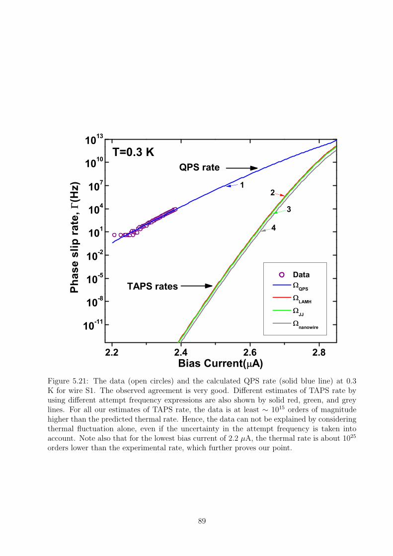
2.2 2.4 2.6 2.8
10-11
10-8
10-5
10-2
101
104
107
1010
1013
TAPS rates
4
Data
QPS
LAMH
JJ
nanowire
Phas
e sl
ip r
ate,
(H
z)
Bias Current( A)
T=0.3 K
12
3
QPS rate
Figure 5.21: The data (open circles) and the calculated QPS rate (solid blue line) at 0.3K for wire S1. The observed agreement is very good. Different estimates of TAPS rate byusing different attempt frequency expressions are also shown by solid red, green, and greylines. For all our estimates of TAPS rate, the data is at least ∼ 1015 orders of magnitudehigher than the predicted thermal rate. Hence, the data can not be explained by consideringthermal fluctuation alone, even if the uncertainty in the attempt frequency is taken intoaccount. Note also that for the lowest bias current of 2.2 µA, the thermal rate is about 1025
orders lower than the experimental rate, which further proves our point.
89
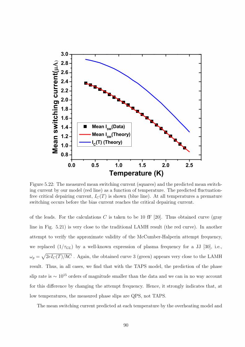
0.0 0.5 1.0 1.5 2.0 2.5
0.81.01.21.41.61.82.02.22.42.62.83.0
Mea
n sw
itchi
ng c
urre
nt(
Temperature (K)
Mean ISW(Data) Mean ISW(Theory) IC(T) (Theory)
Figure 5.22: The measured mean switching current (squares) and the predicted mean switch-ing current by our model (red line) as a function of temperature. The predicted fluctuation-free critical depairing current, IC(T ) is shown (blue line). At all temperatures a prematureswitching occurs before the bias current reaches the critical depairing current.
of the leads. For the calculations C is taken to be 10 fF [20]. Thus obtained curve (gray
line in Fig. 5.21) is very close to the traditional LAMH result (the red curve). In another
attempt to verify the approximate validity of the McCumber-Halperin attempt frequency,
we replaced (1/τGL) by a well-known expression of plasma frequency for a JJ [30], i.e.,
ωp =√
2eIC(T )/~C . Again, the obtained curve 3 (green) appears very close to the LAMH
result. Thus, in all cases, we find that with the TAPS model, the prediction of the phase
slip rate is ∼ 1015 orders of magnitude smaller than the data and we can in no way account
for this difference by changing the attempt frequency. Hence, it strongly indicates that, at
low temperatures, the measured phase slips are QPS, not TAPS.
The mean switching current predicted at each temperature by the overheating model and
90
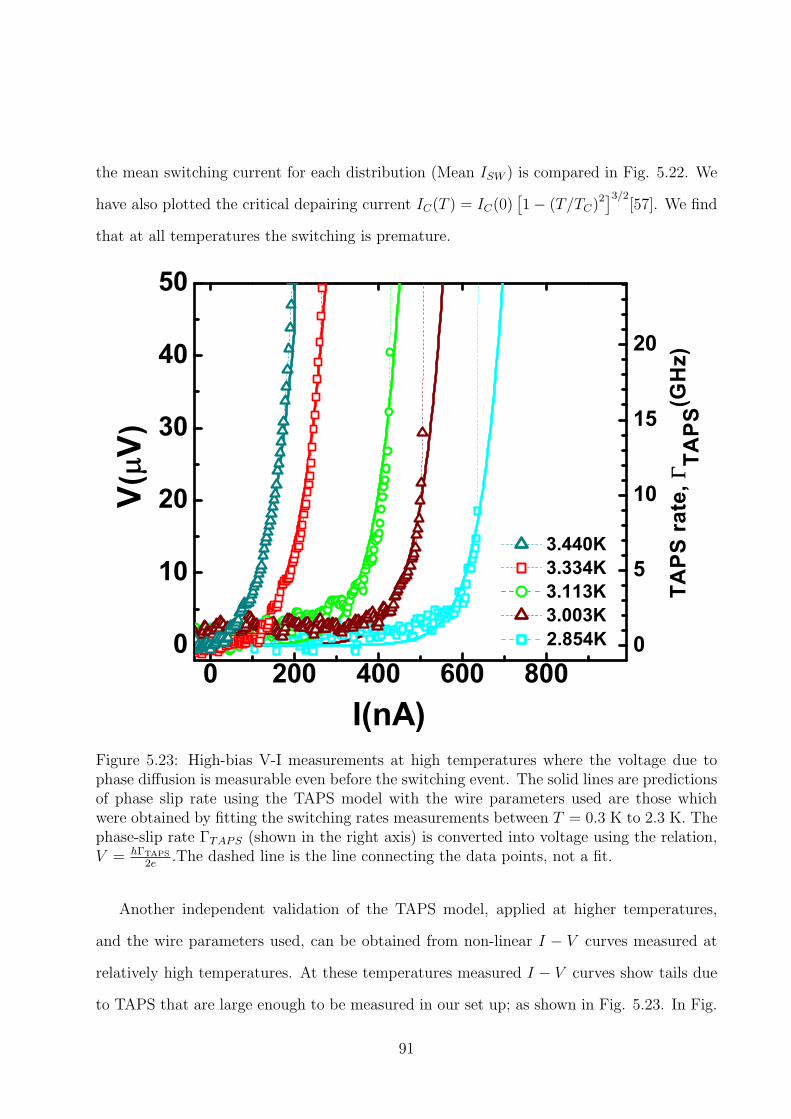
the mean switching current for each distribution (Mean ISW ) is compared in Fig. 5.22. We
have also plotted the critical depairing current IC(T ) = IC(0)[1 − (T/TC)2]3/2
[57]. We find
that at all temperatures the switching is premature.
0 200 400 600 8000
10
20
30
40
50
V(V)
I(nA)
3.440K 3.334K 3.113K 3.003K 2.854K
0
5
10
15
20
TA
PS
rat
e,
TAPS
(GH
z)
Figure 5.23: High-bias V-I measurements at high temperatures where the voltage due tophase diffusion is measurable even before the switching event. The solid lines are predictionsof phase slip rate using the TAPS model with the wire parameters used are those whichwere obtained by fitting the switching rates measurements between T = 0.3 K to 2.3 K. Thephase-slip rate ΓTAPS (shown in the right axis) is converted into voltage using the relation,V = hΓTAPS
2e.The dashed line is the line connecting the data points, not a fit.
Another independent validation of the TAPS model, applied at higher temperatures,
and the wire parameters used, can be obtained from non-linear I − V curves measured at
relatively high temperatures. At these temperatures measured I − V curves show tails due
to TAPS that are large enough to be measured in our set up; as shown in Fig. 5.23. In Fig.
91
5.23, we also plotted the predicted voltage obtained from the TAPS model, using V = hΓTAPS
2e.
For the TAPS rate calculations, the wire parameters used for all our fittings (as shown in
Fig. 3) are kept the same and only the T was varied to get the corresponding TAPS rate.
The measured voltage (or phase-slip rate) and the predicted voltage (or the TAPS rate)
are in good agreement for the five temperatures noted in Fig. 5.23. This agreement indeed
verifies our model for TAPS. The calculation of the TAPS V-I curve is made under the
assumption that the wire temperature equals the bath temperature, i.e., no significant Joule
heating occurs. These type of phase diffusion “tails” on the V-I curves can only be seen at
temperature of about 2.7 K or larger, which is about 10 times higher a temperature than
those where the QPS effects are found.
We can also estimate the zero-bias resistance from our high-bias switching current mea-
surements for very low temperatures, by an extrapolation. Using LAMH theory, we can
convert the zero-bias phase slip rate, Ω (T ) exp(−∆F (T )
kBT
)to resistance. We find that the
resistance drops exponentially from 10−50 to 10−80 Ω for temperatures from 1.1 K to 0.3 K
in the QPS dominated regime for sample S1. This resistance is obviously very small to be
measured in a typical lab setup and can only be estimated from such an extrapolation of the
switching current measurements data. We verified that this resistance is of the same order
as predicted by Golubev-Zaikin (GZ) theory ??, which gives for zero-temperature limit the
result as follows,RQPS = Ω (T ) exp(−ARQL/RNξ(0)) . To get the resistance value of 10−50
to 10−80 Ω we varied A from 2.7 to 4.0 for T = 1.1 K to T = 0.3 K. This is in agreement with
the GZ theory, since they predict that A should be of the order of unity, which we confirm.
92
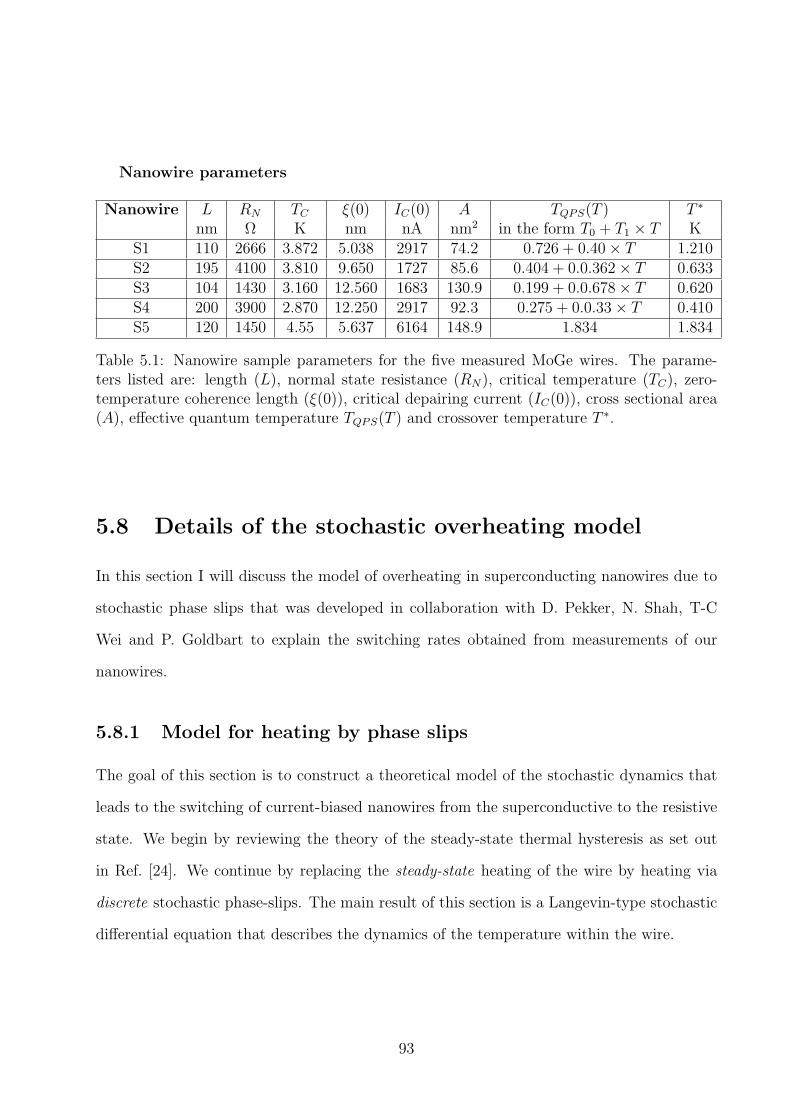
Nanowire parameters
Nanowire L RN TC ξ(0) IC(0) A TQPS(T ) T ∗
nm Ω K nm nA nm2 in the form T0 + T1 × T KS1 110 2666 3.872 5.038 2917 74.2 0.726 + 0.40 × T 1.210S2 195 4100 3.810 9.650 1727 85.6 0.404 + 0.0.362 × T 0.633S3 104 1430 3.160 12.560 1683 130.9 0.199 + 0.0.678 × T 0.620S4 200 3900 2.870 12.250 2917 92.3 0.275 + 0.0.33 × T 0.410S5 120 1450 4.55 5.637 6164 148.9 1.834 1.834
Table 5.1: Nanowire sample parameters for the five measured MoGe wires. The parame-ters listed are: length (L), normal state resistance (RN), critical temperature (TC), zero-temperature coherence length (ξ(0)), critical depairing current (IC(0)), cross sectional area(A), effective quantum temperature TQPS(T ) and crossover temperature T ∗.
5.8 Details of the stochastic overheating model
In this section I will discuss the model of overheating in superconducting nanowires due to
stochastic phase slips that was developed in collaboration with D. Pekker, N. Shah, T-C
Wei and P. Goldbart to explain the switching rates obtained from measurements of our
nanowires.
5.8.1 Model for heating by phase slips
The goal of this section is to construct a theoretical model of the stochastic dynamics that
leads to the switching of current-biased nanowires from the superconductive to the resistive
state. We begin by reviewing the theory of the steady-state thermal hysteresis as set out
in Ref. [24]. We continue by replacing the steady-state heating of the wire by heating via
discrete stochastic phase-slips. The main result of this section is a Langevin-type stochastic
differential equation that describes the dynamics of the temperature within the wire.
93
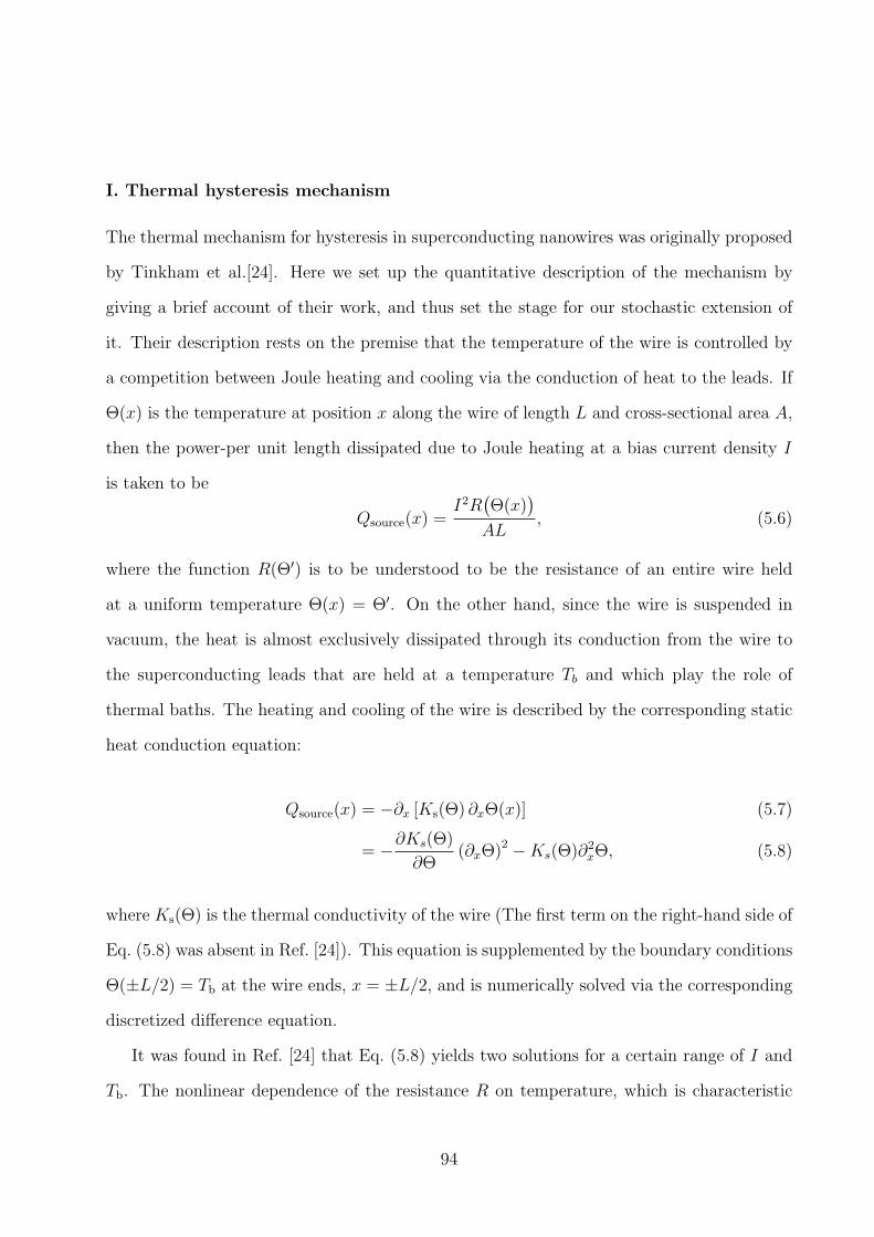
I. Thermal hysteresis mechanism
The thermal mechanism for hysteresis in superconducting nanowires was originally proposed
by Tinkham et al.[24]. Here we set up the quantitative description of the mechanism by
giving a brief account of their work, and thus set the stage for our stochastic extension of
it. Their description rests on the premise that the temperature of the wire is controlled by
a competition between Joule heating and cooling via the conduction of heat to the leads. If
Θ(x) is the temperature at position x along the wire of length L and cross-sectional area A,
then the power-per unit length dissipated due to Joule heating at a bias current density I
is taken to be
Qsource(x) =I2R
(Θ(x)
)
AL, (5.6)
where the function R(Θ′) is to be understood to be the resistance of an entire wire held
at a uniform temperature Θ(x) = Θ′. On the other hand, since the wire is suspended in
vacuum, the heat is almost exclusively dissipated through its conduction from the wire to
the superconducting leads that are held at a temperature Tb and which play the role of
thermal baths. The heating and cooling of the wire is described by the corresponding static
heat conduction equation:
Qsource(x) = −∂x [Ks(Θ) ∂xΘ(x)] (5.7)
= −∂Ks(Θ)
∂Θ(∂xΘ)2 −Ks(Θ)∂2
xΘ, (5.8)
where Ks(Θ) is the thermal conductivity of the wire (The first term on the right-hand side of
Eq. (5.8) was absent in Ref. [24]). This equation is supplemented by the boundary conditions
Θ(±L/2) = Tb at the wire ends, x = ±L/2, and is numerically solved via the corresponding
discretized difference equation.
It was found in Ref. [24] that Eq. (5.8) yields two solutions for a certain range of I and
Tb. The nonlinear dependence of the resistance R on temperature, which is characteristic
94
of a superconducting nanowire, is at the root of this bistability. This bistability in turn
furnishes the mechanism for the thermal hysteresis in the I − V characteristics; the two
solutions correspond to the superconducting (cold solution) and the resistive (hot solution)
branches of the hysteresis loop. To obtain the hysteresis loop at a given bath temperature
Tb, one begins by solving Eq. (5.7) to obtain Θ(x) at a bias current sufficiently low such that
the equation yields only one solution. Next, by using the solution Θ(x) from the previous
step to initialize the equation solver for the next bias current step, the locally stable solution
of Eq. (5.7) is traced out as a function of I by tuning the bias current first up and then
down. The I − V loop is thus traced out by calculating the voltage,
V =
∫ L/2
−L/2
dx IR(Θ(x)
), (5.9)
at each step.
The numerical analysis of Eq. (5.7) requires a knowledge of R(Θ)
and Ks
(Θ), which serve
as the input functions for the theory. In Ref. [24], the linear-response resistance measured
at Tb = Θ was used for R(Θ). However, R depends also on the value of the bias current I.
Henceforth, we shall use R(Θ(x), I
)instead of R
(Θ(x)
).
II. Heating by discrete phase slip events: Derivation of Langevian equation
In the previous subsection we described the static theory of thermal hysteresis as was dis-
cussed in Ref. [24] in the context of experiments on MoGe nanowires. Let us go one step
further and include dynamics by considering the time-dependent heat diffusion equation
Cv(Θ) ∂tΘ(x, t) = ∂x [Ks(Θ) ∂xΘ(x, t)] +Qsource, (5.10)
95
Figure 5.24: Sketch of the overheating model from Ref. [23]. (a) Schematic of the exper-imental configuration described by our model: a superconducting nanowire is suspendedbetween two thermal baths. (b) Sketch showing the attenuation of the order parameter inthe core of a phase-slip. (c) Schematic of the simplified model. All phase slips are taken tooccur in a central (i.e. shaded) segment of length l, which is assumed to be at a uniformtemperature T ; heat is carried away through the end segments, which are assumed to haveno heat capacity. The temperature at the ends of the wire is fixed to be Tb. (d) Sketch of atypical temperature profile.
where the specific heat Cv(Θ) enters as an additional input function. This differential equa-
tion can be derived in the standard way, by using the continuity equation,
∇ · jQ + ∂tQ = Qsource (5.11)
for the heat current,
jQ ≡ −Ks(Θ)∇Θ, (5.12)
96
together with the energy density,
Q ≡∫ Θ(x)
Cv(Θ′)dΘ′. (5.13)
However, as long as we assume that the wire is heated by the source term given by
Eq. (5.6), the dynamic formulation turns out to be inadequate for our purposes, as should
become clear from our analysis and results. Such a source term assumes that the wire is being
continually heated locally as a result of its resistivity R(Θ(x), I)A/L at any given position x
along the wire. Is this assumption of continual Joule heating correct? To answer this question
we need to deconstruct the resistance and get to its root. It needs to be emphasized that
it is the resistive phase-slip fluctuations that are responsible for the characteristic resistance
of a quasi-one dimensional wire. Therefore, one should thus consider the Joule heating as
being caused by individual, discrete phase-slip events.
Let us then explicitly consider discrete phase-slip events (labelled by i) that take place
one at a time at random instants of time ti, and are centered at random spatial locations xi.
By using the Josephson relation
dφ
dt=
2eV
ℏ=
2πV
Φ0
(5.14)
relating the voltage pulse V (t) to the rate of change of the end-to-end phase difference across
the wire φ, we arrive at the work done on the wire by a phase slip, viz.,
Qps =
∫dt IV = I
∫ 2π
0
dφ~
2e= Φ0I, (5.15)
where Φ0 = h/2e is the superconducting flux quantum. Hence, a single phase slip (or
anti-phase slip), which corresponds to a decrease (or increase) of φ by 2π, will heat (or
cool) the wire by a “quantum” of energy Qps. Using this result, we can now write down a
97
time-dependent stochastic source term,
Qsource(x, t) ≡Qps
A
∑
i
σi F (x− xi) δ(t− ti), (5.16)
where F (x−xi) is a spatial form factor, normalized to unity, representing the relative spatial
distribution of heat produced by the ith phase-slip event, and σi = ±1 for phase (anti-phase)
slips. The probability per unit time Γ± for anti-phase (phase) slips to take place depends
on the local temperature Θ(x, t) and the current I.
Now, instead of using the continual Joule heating source term, Eq. (5.6), let us use the
source term given by Eq. (5.16). Instead of being a deterministic differential equation, the
heat diffusion equation (5.10) becomes a stochastic differential equation for T (x, t). We thus
have a Langevin equation with stochasticity, in one space and one time dimension, with a
“noise” term that is characteristic of a jump process.
Let us try to understand the connection between the two source terms. By using the
Josephson relation (5.14), we can express
R(Θ, I) =V
I=
1
I
Φ0
2π
dφ
dt=
Φ0Γ(Θ, I)
I(5.17)
and use it to rewrite the continual Joule-heating source term, Eq. (5.6), as
Qsource =Qps Γ(Θ, I)
AL, (5.18)
where Γ ≡ Γ−−Γ+. Let us assume that a phase slip only affects its local neighborhood, i.e.,
F (x− xi) ∼ δ(x− xi). Then, if we take the continuum time-limit of Eq. (5.16) by assuming
that the phase-slips are very frequent and that Qps → 0, the two source terms would indeed
become equivalent (as can also be seen formally by taking the limit Φ0 → 0).
We now make a brief remark about the switching current. The static theory of hysteresis
that was discussed in the previous subsection has a single, well-defined value of the switching
98
current, which corresponds to the value of the bias current at which the low-temperature
(superconductive) solution becomes unstable. On the other hand, we see from the theory
discussed in the present subsection that the randomness in xi and ti generates a stochasticity
in the switching process. The full implications of the stochastic dynamical theory will be
discussed in the following sections.
III. Simplified model: Reduced Langevin equation
In principle, one can proceed to study the physics of the stochastic switching dynamics
of a current-biased nanowire by using the dynamics of Eq. (5.10) together with stochastic
source Eq. (5.16), both derived in the previous subsection. In practice, however, it is not
easy to solve the full Langevin equation with both spatial and temporal randomness. In
this subsection we derive a simplified model, and argue that it is capable of capturing the
physics essential for our purposes.
We concentrate on wires that are in the dirty limit, for which the mean free path is
much shorter than the coherence length, which is shorter than the charge imbalance length
required for carrier thermalization, which itself is somewhat shorter than L. In addition
to restrictions on length-scales, we assume that the time for a phase-slip (∼ τGL) and the
quasi-particle thermalization time τE are both smaller than the wire cooling time, i.e., the
time it takes the heat deposited in the middle of the wire by a phase-slip to diffuse out of
the wire.
We will make a series of simplifications as follows:
1. Due to the presence of the superconducting leads at two ends as well as edge effects,
it is more likely that the phase-slip fluctuations in the wire are centered away from
the wire edges. We thus assume that the source term is restricted to a region near the
center of the wire.
2. We assume that the heating takes place within a central segment of length l, to which
99
a uniform temperature T is assigned. Note that the total length L may be allowed to
differ slightly from the geometric length of the wire, in order to compensate for the
temperature gradients in the lead at the wire attachment point.
3. We assume that the heat is conducted away through the end segments, each of which
are of length (L− l)/2. As an additional simplification, we ignore the heat capacity of
these end segments.
4. To simplify the problem further, we make use of the fact that the probability per
unit time (i.e., the characteristic rate) Γ+ for an anti-phase slip to take place is much
smaller than the rate Γ− for a phase slip to take place, and we thus ignore the process of
cooling by anti-phase slips. To account indirectly for their presence, we use a reduced
rate Γ ≡ Γ− − Γ+ instead of Γ−. This ensures that the discrete expression for Q
correctly reduces to the continual Joule-heating expression.
With the simplified model defined above, the description of superconducting nanowires
reduces to a stochastic ordinary differential equation for the time-evolution of the tempera-
ture T of the central segment:
dT
dt= −α(T, Tb)(T − Tb) + η(T, I)
∑
i
δ(t− ti). (5.19)
This equation can be though of as a reduced Langevin-type equation which is the counterpart
of the full Langevin-type Eq. (5.10) with the source term Eq. (5.16) in the un-simplified
model. The second term on the RHS of Eq. (5.19) corresponds to (stochastic) heating
by phase slips, and the first to (deterministic) cooling as a result of conduction of heat
from the central segment to the external bath via the two end-segments. The temperature-
dependent cooling rate, α(T, Tb), is obtained by comparing the heat currents through the
end segments to the thermal mass of the central segment, where the heat currents through
the end segments are found by solving the heat equation in the end segments subject to the
100
boundary conditions that T (0) = T (L) = Tb and T (L−l2
) = T (L− L−l2
) = T .
α(T, Tb) ≡4
l(L− l)Cv(T )
1
T − Tb
∫ T
Tb
dT ′Ks(T′). (5.20)
If Ti and Tf are temperatures of the central segment before and after a phase slip then we
can express the temperature ‘impulse’ due to a phase slip, i.e., Tf − Ti ≡ η(Ti, I) ≡ η(Tf, I),
as function of either Ti or Tf (depending on the context) by using
A l
∫ Tf
Ti
Cv(T′) dT ′ = Qps. (5.21)
To summarize, in this section we have derived a simplified model that is described by
the reduced Langevin equation (5.19). The central assumption that we used to build this
simplified model is that phase-slips predominantly occur in the center of the nanowire, or
at least their exact spatial locations are unimportant. This assumption is appropriate for
shorter nanowires, in which we do not have several distinct locations along the wire at which
a switching event may nucleate. Specifically, if the wire length does not greatly exceed
the charge imbalance length (which itself is assumed to be much larger than the coherence
length), then independent of where a phase-slip occurs the temperature profile in the wire
after the phase slip will be similar, and we can use our simplified time-only model.
5.8.2 Input functions and parameters
In this appendix we list the models for phase-slip rate, specific heat, and thermal conductivity
that go into the stochastic heat equation (5.10).
101
Phase-slip rate
We begin by considering the phase slip rate. For the TAPS rate we have used the LAMH
model, including the non-linear current response
ΓTAPS(I, T ) = Γ−,TAPS(I, T ) − Γ+,TAPS(I, T ) (5.22)
Γ±,TAPS(I, T ) =Ω±(I, T ) exp
(−∆F±(I, T )
kBT
)(5.23)
where, + and − indicates whether the phase-slip results in current rise or current drop
respectively. The phase-slip barrier at bias current I and temperature T is
C1(T ) =3√
3
8
~
2eIc(T ) (5.24)
∆F−(T ) = C1(T )
(8
3
√2√
1 − 3k2 − 8k(1 − k2) arctan
√1 − 3k2
√2k
)(5.25)
∆F+(T ) = C1(T )
(8
3
√2√
1 − 3k2 + 8k(1 − k2)
[π − arctan
√1 − 3k2
√2k
])(5.26)
where the phase gradient k is the real solution of
I
Ic(T )= k(1 − k2), (5.27)
and the temperature dependent critical current Ic(T ) [57] is expressed in terms of the wire
length L, critical temperature Tc, zero temperature coherence length ξ(0), and the normal
state resistance of the wire Rn [58]
IC(T ) = (92µA)LTC
Rnξ0
(1 −
(T
TC
)2)3/2
. (5.28)
102
We approximate the prefactor Ω±(I, T ) via
Ω(T ) =
√3
2π3/2
L
ξ(T )τ(T )
(∆F (I = 0, T )
kBT
)1/2
(5.29)
Ω−(I, T ) = (1 −√
3k)15/4(1 + k2/4)Ω(T ) (5.30)
Ω+(I, T ) = Ω(T ). (5.31)
In the presence of a bias current, the “+” phase slips are exponentially more rare than
the “-” phase-slips. Therefore, we keep the current corrections to the prefactor for the “-”
phase-slips, but not the “+” phase slips. Thus we get an approximation which is works in
both linear-response regime where the current correction is irrelevant and in the high bias
regime where “+” phase slips are rare. We estimate the temperature dependent coherence
length and the Ginzburg-Landau time via
ξ(T ) = ξ(0)√
1 − (T/TC)4/(1 − (T/TC)2) (5.32)
τ(T ) = π~/8kB(TC − T ). (5.33)
Thus, we can express the phase slip rate via L, Rn, ξ(0), TC .
To obtain the quantum phase-slip rate, we replace T in the denominator of the exponen-
tial function of Eq. (5.23) by the effective temperature Teff = T0 + T1T , where T0 and T1 are
treated as fitting parameters.
Heat capacity and thermal conductivity
Unfortunately, there is no direct experimental data on the heat capacity and thermal con-
ductivity of current carrying superconducting nanowires. The diameter of the wires used in
experiments is comparable to ξ(0). Thus, thermodynamic properties of these wires should be
somewhere between those of a bulk superconductor and a normal metal. Therefore, for the
purposes of computing the thermodynamic functions we model the wire as being composed
103
of a BCS superconducting wire with cross-section A1 in parallel to a normal metal wire with
cross-section A2.
The BCS and Fermi liquid expressions for heat capacity [30] are
Cv,BCS = −2N0
T
∫Ek
dfk
d(βEk)
(Ek + β
dEk
dβ
)dξk, (5.34)
Cv,FL =2
3π2N0k
2BT, (5.35)
where β = 1/kBΘ, Ek =√ξ2k + ∆2(Θ), fk is the Fermi function and ∆(Θ) is obtained from
the BCS gap equation. Thus the total heat capacity of the wire is
Cv =A1Cv,BCS + A2Cv,FL
A1 + A2
. (5.36)
Similarly, the dirty limit BCS [59] and Fermi liquid expressions for thermal conductivity
are
Ks,BCS(Θ) = 2N0D
∫∞
∆
sech2[
ǫ2kBΘ
]
2kBΘ
ǫ2
kBΘdǫ, (5.37)
Ks,FL(Θ) =L0ΘL
ARn
(5.38)
where D is the diffusion constant (for MoGe D ∼ 1 cm2/s [51]), and L0 = π2k2B/3e
2. The
total heat conductivity is
Ks =A1Ks,BCS + A2Ks,FL
A1 + A2
. (5.39)
The fitting parameters describing heat capacity and heat conductivity are the cross-
sections A1 and A2, and the TC of the nanowire.
104
5.8.3 Comparison with experimental data
In this section, we compare results from our experiments with predictions of our theory. We
show that our theory is both qualitatively and quantitatively consistent with experimen-
tal observations. The main implication of the comparison are: (1) the switching-current
distribution-width does indeed increase as the temperature is decreased; (2) there is a sin-
gle phase-slip-to-switch regime at low temperatures; and (3) thermally activated phase-slips,
alone, are insufficient to fit the dependence of the mean switching time on the bias current at
low temperatures which suggests that we should include quantum phase-slips; upon including
quantum phase-slips phenomenologically, we can obtain good fits to the experimental data
in the low temperature regime as well. This section is structured as follows. To establish
the validity of the thermal hysteresis model, we begin by analyzing the I-V hysteresis loops.
Next, we qualitatively analyze the experimentally measured switching current distribution.
We continue with a quantitative analysis of the experimental data on the mean switching
rate.
I. I − V hysteresis loops
We begin our analysis by comparing the qualitative features of the experimentally measured
and theoretically computed current-voltage characteristics. Experimentally it is found that
at high temperatures there is no hysteresis. As Tb is lowered, a hysteresis loop gradually
opens up. Next, as the temperature is lowered even further, the switching current (i.e.,
the bias current at the superconducting-resistive transition) grows gradually, whilst the re-
trapping current (i.e., the bias current at the resistive-superconducting transition) remains
almost unchanged. This behavior is consistent with the experimental observations and the
theory of Ref. [24], where this is also qualitatively explained as follows. Switching is con-
trolled by the properties of the low-temperature (i.e., superconducting-like) solution which
depends strongly on the temperature of the bath Tb. On the other hand, re-trapping is
largely a property of the hotter (i.e., resistive) state, and thus has only a weak dependence
105
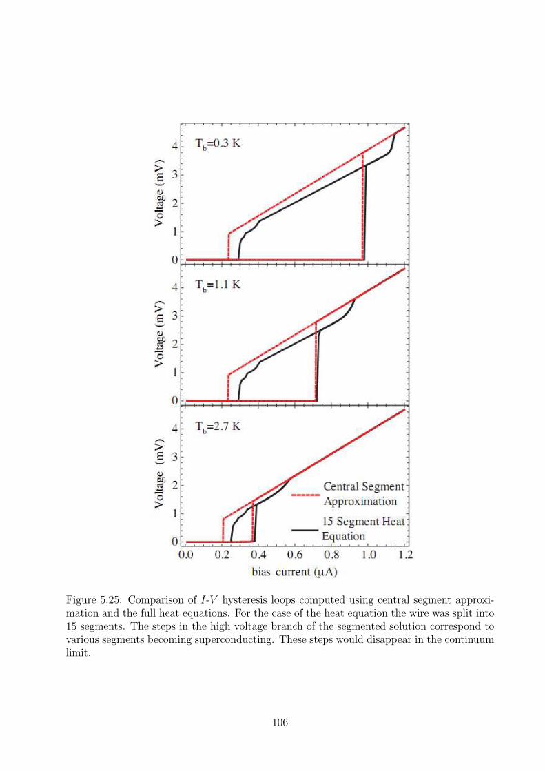
Figure 5.25: Comparison of I-V hysteresis loops computed using central segment approxi-mation and the full heat equations. For the case of the heat equation the wire was split into15 segments. The steps in the high voltage branch of the segmented solution correspond tovarious segments becoming superconducting. These steps would disappear in the continuumlimit.
106
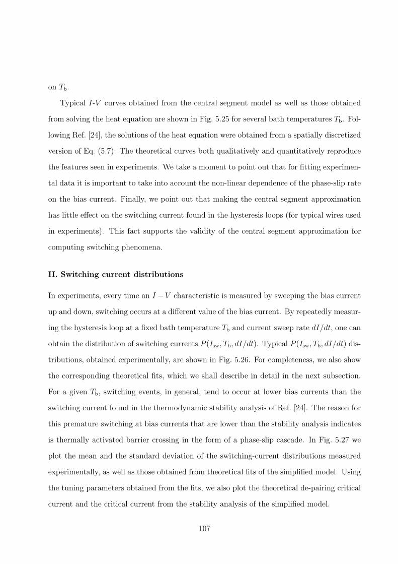
on Tb.
Typical I-V curves obtained from the central segment model as well as those obtained
from solving the heat equation are shown in Fig. 5.25 for several bath temperatures Tb. Fol-
lowing Ref. [24], the solutions of the heat equation were obtained from a spatially discretized
version of Eq. (5.7). The theoretical curves both qualitatively and quantitatively reproduce
the features seen in experiments. We take a moment to point out that for fitting experimen-
tal data it is important to take into account the non-linear dependence of the phase-slip rate
on the bias current. Finally, we point out that making the central segment approximation
has little effect on the switching current found in the hysteresis loops (for typical wires used
in experiments). This fact supports the validity of the central segment approximation for
computing switching phenomena.
II. Switching current distributions
In experiments, every time an I −V characteristic is measured by sweeping the bias current
up and down, switching occurs at a different value of the bias current. By repeatedly measur-
ing the hysteresis loop at a fixed bath temperature Tb and current sweep rate dI/dt, one can
obtain the distribution of switching currents P (Isw, Tb, dI/dt). Typical P (Isw, Tb, dI/dt) dis-
tributions, obtained experimentally, are shown in Fig. 5.26. For completeness, we also show
the corresponding theoretical fits, which we shall describe in detail in the next subsection.
For a given Tb, switching events, in general, tend to occur at lower bias currents than the
switching current found in the thermodynamic stability analysis of Ref. [24]. The reason for
this premature switching at bias currents that are lower than the stability analysis indicates
is thermally activated barrier crossing in the form of a phase-slip cascade. In Fig. 5.27 we
plot the mean and the standard deviation of the switching-current distributions measured
experimentally, as well as those obtained from theoretical fits of the simplified model. Using
the tuning parameters obtained from the fits, we also plot the theoretical de-pairing critical
current and the critical current from the stability analysis of the simplified model.
107
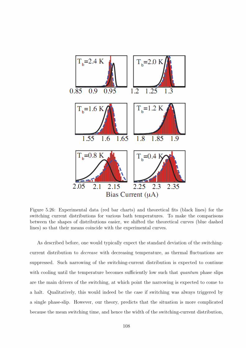
Figure 5.26: Experimental data (red bar charts) and theoretical fits (black lines) for theswitching current distributions for various bath temperatures. To make the comparisonsbetween the shapes of distributions easier, we shifted the theoretical curves (blue dashedlines) so that their means coincide with the experimental curves.
As described before, one would typically expect the standard deviation of the switching-
current distribution to decrease with decreasing temperature, as thermal fluctuations are
suppressed. Such narrowing of the switching-current distribution is expected to continue
with cooling until the temperature becomes sufficiently low such that quantum phase slips
are the main drivers of the switching, at which point the narrowing is expected to come to
a halt. Qualitatively, this would indeed be the case if switching was always triggered by
a single phase-slip. However, our theory, predicts that the situation is more complicated
because the mean switching time, and hence the width of the switching-current distribution,
108
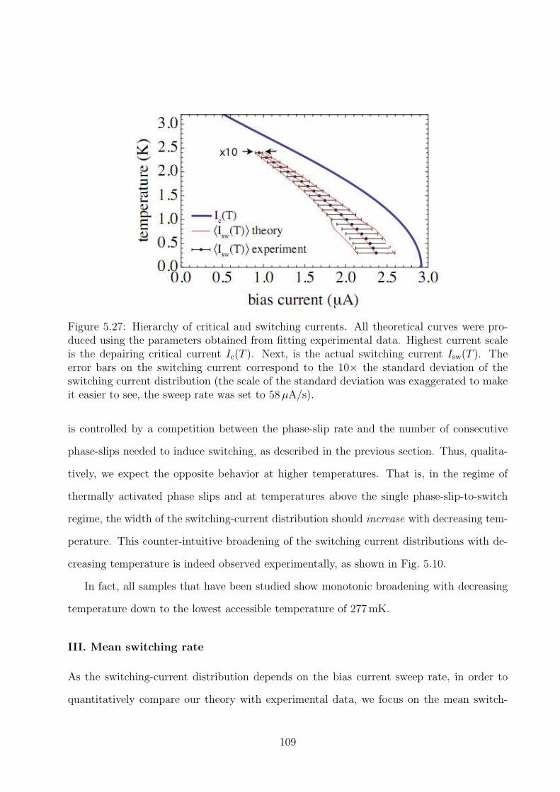
Figure 5.27: Hierarchy of critical and switching currents. All theoretical curves were pro-duced using the parameters obtained from fitting experimental data. Highest current scaleis the depairing critical current Ic(T ). Next, is the actual switching current Isw(T ). Theerror bars on the switching current correspond to the 10× the standard deviation of theswitching current distribution (the scale of the standard deviation was exaggerated to makeit easier to see, the sweep rate was set to 58µA/s).
is controlled by a competition between the phase-slip rate and the number of consecutive
phase-slips needed to induce switching, as described in the previous section. Thus, qualita-
tively, we expect the opposite behavior at higher temperatures. That is, in the regime of
thermally activated phase slips and at temperatures above the single phase-slip-to-switch
regime, the width of the switching-current distribution should increase with decreasing tem-
perature. This counter-intuitive broadening of the switching current distributions with de-
creasing temperature is indeed observed experimentally, as shown in Fig. 5.10.
In fact, all samples that have been studied show monotonic broadening with decreasing
temperature down to the lowest accessible temperature of 277 mK.
III. Mean switching rate
As the switching-current distribution depends on the bias current sweep rate, in order to
quantitatively compare our theory with experimental data, we focus on the mean switch-
109
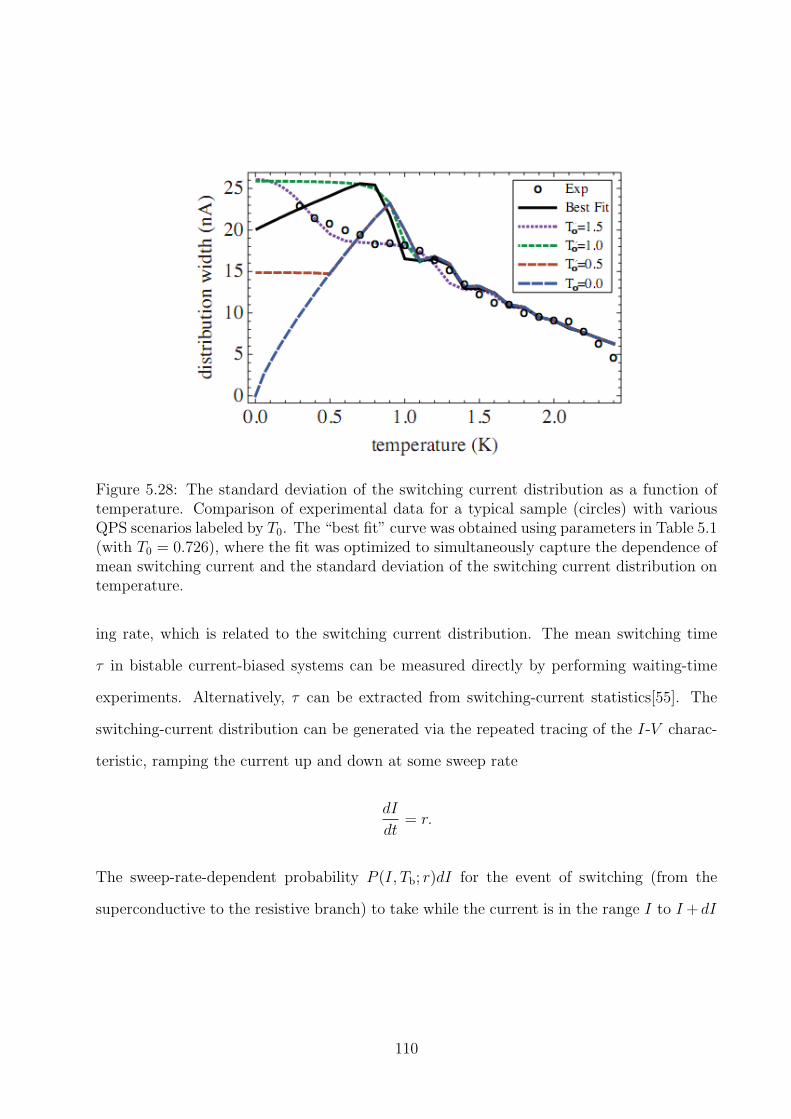
Figure 5.28: The standard deviation of the switching current distribution as a function oftemperature. Comparison of experimental data for a typical sample (circles) with variousQPS scenarios labeled by T0. The “best fit” curve was obtained using parameters in Table 5.1(with T0 = 0.726), where the fit was optimized to simultaneously capture the dependence ofmean switching current and the standard deviation of the switching current distribution ontemperature.
ing rate, which is related to the switching current distribution. The mean switching time
τ in bistable current-biased systems can be measured directly by performing waiting-time
experiments. Alternatively, τ can be extracted from switching-current statistics[55]. The
switching-current distribution can be generated via the repeated tracing of the I-V charac-
teristic, ramping the current up and down at some sweep rate
dI
dt= r.
The sweep-rate-dependent probability P (I, Tb; r)dI for the event of switching (from the
superconductive to the resistive branch) to take while the current is in the range I to I + dI
110
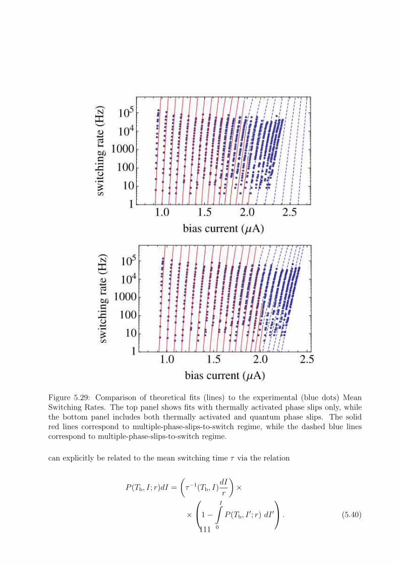
Figure 5.29: Comparison of theoretical fits (lines) to the experimental (blue dots) MeanSwitching Rates. The top panel shows fits with thermally activated phase slips only, whilethe bottom panel includes both thermally activated and quantum phase slips. The solidred lines correspond to multiple-phase-slips-to-switch regime, while the dashed blue linescorrespond to multiple-phase-slips-to-switch regime.
can explicitly be related to the mean switching time τ via the relation
P (Tb, I; r)dI =
(τ−1(Tb, I)
dI
r
)×
×
1 −
I∫
0
P (Tb, I′; r) dI ′
. (5.40)
111
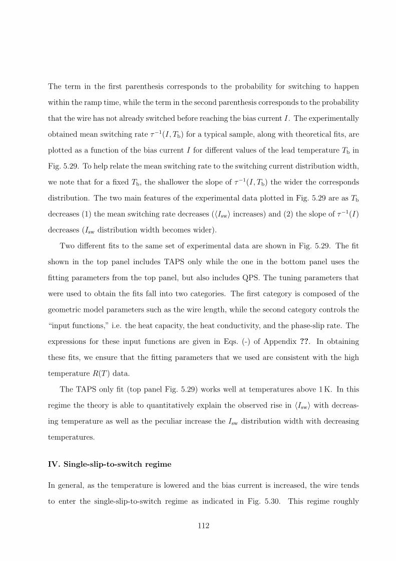
The term in the first parenthesis corresponds to the probability for switching to happen
within the ramp time, while the term in the second parenthesis corresponds to the probability
that the wire has not already switched before reaching the bias current I. The experimentally
obtained mean switching rate τ−1(I, Tb) for a typical sample, along with theoretical fits, are
plotted as a function of the bias current I for different values of the lead temperature Tb in
Fig. 5.29. To help relate the mean switching rate to the switching current distribution width,
we note that for a fixed Tb, the shallower the slope of τ−1(I, Tb) the wider the corresponds
distribution. The two main features of the experimental data plotted in Fig. 5.29 are as Tb
decreases (1) the mean switching rate decreases (〈Isw〉 increases) and (2) the slope of τ−1(I)
decreases (Isw distribution width becomes wider).
Two different fits to the same set of experimental data are shown in Fig. 5.29. The fit
shown in the top panel includes TAPS only while the one in the bottom panel uses the
fitting parameters from the top panel, but also includes QPS. The tuning parameters that
were used to obtain the fits fall into two categories. The first category is composed of the
geometric model parameters such as the wire length, while the second category controls the
“input functions,” i.e. the heat capacity, the heat conductivity, and the phase-slip rate. The
expressions for these input functions are given in Eqs. (-) of Appendix ??. In obtaining
these fits, we ensure that the fitting parameters that we used are consistent with the high
temperature R(T ) data.
The TAPS only fit (top panel Fig. 5.29) works well at temperatures above 1 K. In this
regime the theory is able to quantitatively explain the observed rise in 〈Isw〉 with decreas-
ing temperature as well as the peculiar increase the Isw distribution width with decreasing
temperatures.
IV. Single-slip-to-switch regime
In general, as the temperature is lowered and the bias current is increased, the wire tends
to enter the single-slip-to-switch regime as indicated in Fig. 5.30. This regime roughly
112
Figure 5.30: Map of N(Tb, I) the number of consecutive phase slips required to overcome thebarrier and induce the wire to switch as a function of bias current I and bath temperatureTb. The three solid lines indicate the contours along which Γ−1
sw (the mean switching rate)is 1, 103, and 106 s−1. Similarly, the three dashed lines indicate the contours along whichthe phase slip rate is 1, 103, and 106 s−1. For comparison, the depairing critical current isindicated by the dashed-dotted line.
corresponds to the region of the (I, T ) plane where a single phase slip heats up the wire to
TC(I), and thus the boundaries of this regime are primarily determined by the heat capacity
of the wire. When working within regime, switching current statistics correspond directly
to the phase-slip statistics.
Theoretical fitting indicates that at temperatures below 1 K the wire enters the single-
phase-slip-to-switch regime. This regime is indicated by the switch of the theory curves
from solid red lines to dashed blue lines in Fig. 5.29. In the absence of quantum phase
slips, in this regime the Isw distribution width should follow a more conventional behavior
113
and decreases with temperature. This corresponds to the increase in the slope of the mean
switching rate curves with decreasing temperature in the single-slip-to-switch regime (see
top panel of Fig. 5.29).
However, experimentally the distribution width seems to increase monotonically as the
temperature is lowered, even in the single-slip-to-switch regime. This behavior suggests that
there is an excess of phase slips at low temperatures.
V. Quantum phase-slip scenarios
We expect that at low temperatures quantum phase-slips can strongly contribute to the
switching rate. We model the presence of QPS by adding their rate to the rate of TAPS to
obtain the total phase-slip rate which goes into our model
Γtotal(I, T ) = ΓTAPS(I, T ) + ΓQPS(I, T ). (5.41)
To model the QPS rate, ΓTAPS(I, T ), we replace T → T0 + T1T in ΓQPS(I, T ). Here, T0 and
T1 are both treated as fitting parameters. Letting T1 be nonzero does somewhat improve
the quality of our fits.
We can envision several scenarios for the effect of QPSs on the switching current dis-
tributions, these are summarized in Fig. 5.28. In the absence of QPS, upon lowering the
temperature, once the single-slip-to-switch regime is reached the distribution width will start
decreasing with temperature. This type of behavior is demonstrated by the T0 = 0 line in
Fig. 5.28. However, in the presence of QPS, the distribution width is expected to satu-
rate at low temperature, with the saturation value controlled by T0. If, upon cooling, the
single-slip-to-switch regime is reached before the temperature reaches T0, we expect the dis-
tribution width increases and then decrease before saturating with decreasing temperature
(T0 = 0.5 K curve in Fig. 5.28). On the other hand, if T0 is reached before the single-slip-
to-switch regime, we expect the distribution width increases monotonically with decreasing
114
temperature (T0 = 1.0, 1.5 K curves in Fig. 5.28).
To include QPS in our fitting, we started with parameters obtained by fitting the mean
switching rate curves at high temperatures (T > 1 K) as described in the previous subsection
(See top panel of Fig. 5.29). Next we optimized T0 and T1 to obtain best possible fit to the
mean switching rate curves at low temperatures as well. The optimal values thus obtained
were T0 = 0.726 K and T1 = 0.4, which corresponds to the fit shown in the bottom panel of
Fig. 5.29 and the curve labeled “best fit” in Fig. 5.28.
To fit experimental data, we must be able to simultaneously match both the mean and
the standard deviation of the switching current distribution as a function of temperature.
However, we have not been able to get quantitative agreement with both, simultaneously,
in the low temperature regime. The parameter values T0 = 0.726 K and T1 = 0.4 result in
a good fit of the mean but not the standard deviation (see Fig. 5.29 and 5.28), while the
values T0 = 1.5 K and T1 = 0 result in a good fit of the standard deviation (see Fig. 5.28)
but not the mean (not shown).
We conclude this section by noting that our fitting seems to favor the QPS scenario where
the single-slip-to-switch regime occurs at a lower temperature than T0.
115
Chapter 6
Multiple-retrapping process in high-TcJosephson junctions
In this chapter we report measurements of switching current distribution (SWCD) from
a phase diffusion branch (PDB) to a quasiparticle tunneling branch (QTB) as a function
of temperature in a cuprate-based intrinsic Josephson junction. Contrary to the thermal-
activation model, the width of the SWCD increases and the corresponding switching rate
shows a nonlinear behavior with a negative curvature in a semi-logarithmic scale with de-
creasing temperature, down to 1.5 K. Based on the multiple retrapping model, we quanti-
tatively demonstrate that the frequency-dependent junction quality factor, representing the
energy dissipation in a phase diffusion regime, determines the observed temperature depen-
dence of the SWCD and the switching rate. We also show that a retrapping process from
the QTB to the PDB is related to the low-frequency limit damping.
This work was done in collaboration with Myung-Ho Bae, Hu-Jong Lee and A. Bezryadin.
The results and text of this chapter were published under the title “Multiple-Retrapping
Process in Phase-Diffusion Regime of High-Tc Intrinsic Josephson Junction” and are repeated
here. reprinted with permission from Myung-Ho Bae, M. Sahu, Hu-Jong Lee, A. Bezryadin
Phys. Rev. B 79, 104509 (2009) Copyright 2009 by the American Physical Society.
6.1 Introduction
The escape of a system trapped in a metastable state governs the reaction rate in various
dynamical systems, where the escape is made by a noise-assisted hopping [60]. In the
case of a Josephson junction (JJ), a thermal noise induces an escape of a phase particle
116
representing the system from a local minimum of the potential well. In an underdamped JJ
with hysteresis in the voltage-current (V-I) characteristics a single escaping event induces
a switching from a zero-voltage phase-trapped state to a finite-voltage phase-rolling state,
which gives a switching current, ISW [55]. In an overdamped JJ without hysteresis, however,
the energy of an escaped phase particle is strongly dissipated during its motion so that
the particle is retrapped in another local minimum of the potential. The phase particle
repeats this thermally activated escape and retrapping process, i.e., the multiple-retrapping
process in an overdamped JJ. It results in a phase-diffusion branch (PDB) with a small
but finite voltage for a bias current below the critical current [30]. A hysteretic JJ can
also evolve into this multiple-retrapping regime if the temperature is sufficiently high [61].
Recently, this phase-retrapping phenomenon in JJ’s with hysteresis, including cuprate-based
intrinsic Josephson junctions (IJJ’s), has been intensively studied in association with the
temperature dependence of a switching current distribution (SWCD) [62, 63, 64]. The
main finding of these studies is that the retrapping process in the hysteretic JJ modifies
the switching dynamics, in such a way as to reduce the width of SWCD with increasing
temperature. This SWCD behavior, contrasting to the usual thermal activation model, has
also been suggested to be caused by the enhanced dissipation due to a frequency-dependent
impedance [65]. The impedance of the measurement lines (ZL = 50∼100 Ω) is the main
source of the high-frequency dissipation. As the dissipation of a JJ is represented by its
quality factor, the previous studies have focused only on the moderately damped regime of
quality factor ∼5, where the V -I curves with the SWCD’s do not exhibit PDB’s because the
rate of the phase diffusion is too low to show a finite voltage at the temperatures studied.
Thus, although the PDB itself has been extensively studied in conventional JJ and IJJ
systems [66, 67, 61, 68, 69], the switching dynamics between a PDB and a quasiparticle-
tunneling branch (QTB) has not been clearly resolved in terms of the quality factor.
Here we report switching from the PDB to the QTB in IJJs of Bi2Sr2CaCu2O8+x (Bi-
2212) at various temperatures below T = 4.2 K. Temperature dependence of the switching
117
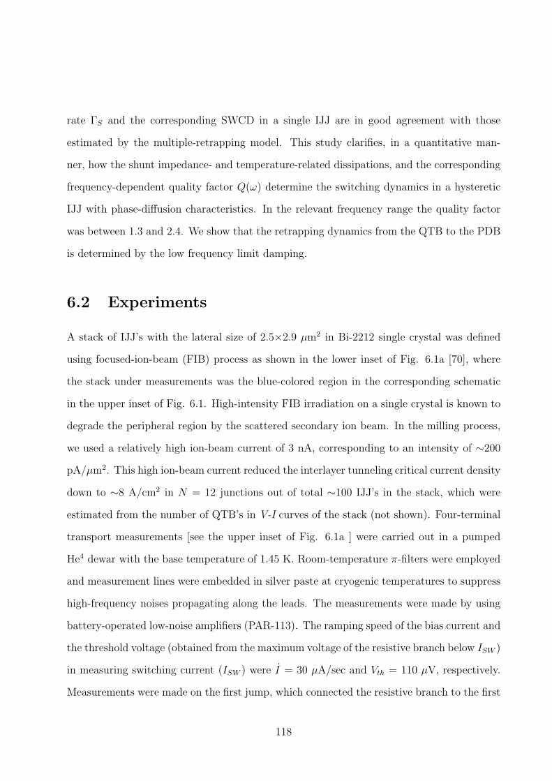
rate ΓS and the corresponding SWCD in a single IJJ are in good agreement with those
estimated by the multiple-retrapping model. This study clarifies, in a quantitative man-
ner, how the shunt impedance- and temperature-related dissipations, and the corresponding
frequency-dependent quality factor Q(ω) determine the switching dynamics in a hysteretic
IJJ with phase-diffusion characteristics. In the relevant frequency range the quality factor
was between 1.3 and 2.4. We show that the retrapping dynamics from the QTB to the PDB
is determined by the low frequency limit damping.
6.2 Experiments
A stack of IJJ’s with the lateral size of 2.5×2.9 µm2 in Bi-2212 single crystal was defined
using focused-ion-beam (FIB) process as shown in the lower inset of Fig. 6.1a [70], where
the stack under measurements was the blue-colored region in the corresponding schematic
in the upper inset of Fig. 6.1. High-intensity FIB irradiation on a single crystal is known to
degrade the peripheral region by the scattered secondary ion beam. In the milling process,
we used a relatively high ion-beam current of 3 nA, corresponding to an intensity of ∼200
pA/µm2. This high ion-beam current reduced the interlayer tunneling critical current density
down to ∼8 A/cm2 in N = 12 junctions out of total ∼100 IJJ’s in the stack, which were
estimated from the number of QTB’s in V-I curves of the stack (not shown). Four-terminal
transport measurements [see the upper inset of Fig. 6.1a ] were carried out in a pumped
He4 dewar with the base temperature of 1.45 K. Room-temperature π-filters were employed
and measurement lines were embedded in silver paste at cryogenic temperatures to suppress
high-frequency noises propagating along the leads. The measurements were made by using
battery-operated low-noise amplifiers (PAR-113). The ramping speed of the bias current and
the threshold voltage (obtained from the maximum voltage of the resistive branch below ISW )
in measuring switching current (ISW ) were I = 30 µA/sec and Vth = 110 µV, respectively.
Measurements were made on the first jump, which connected the resistive branch to the first
118
Figure 6.1: (a) R vs T curve of the sample stack, where Tc of the crystal is indicatedby the right arrow. The left arrow indicates the critical temperature of the phase-diffusivejunctions. Upper inset of (a): schematics for the sample and the measurement configurations.Lower inset of (a): Scanning electron microscope image of the measured sample. (b) V-Icharacteristics at various temperatures of the Bi-2212 IJJs stack. The upward and downwardarrows indicate the switching and the return currents, respectively, at T = 15.1 K, where aresistance of the QTB, Rqp∼35 kΩ. Inset of (b): V-I curves of the sample at T = 1.8 K,3.3 K, and 4.2 K, show the resistance increase with cooling in this region of temperature,possibly due to presence of a normal segment in the stack.
QTB of the weakest junction in the stack. For each distribution, 10000 switching events
were recorded with the current resolution of 90 pA.
119
6.3 Results and discussion
Fig. 6.1(a) shows the R vs T curve of our stacked junction device, which reveals a super-
conducting transition at Tc = 90 K as indicated by the right arrow. The c-axis tunneling
nature in the Bi-2212 stacked junctions is evident by the increasing resistance with decreas-
ing temperature above Tc. The resistance in the temperature range 54 K<T<Tc originates
from weakly superconducting layers [71], which have a suppressed critical temperature due
to a degradation caused by the high-intensity ion beam in the FIB process. The critical
temperature of these layers is about 54 K as shown by the left arrow. The resistance at
T<54 K, however, does not vanish completely, even down to T = 10 K, which is attributed
to the phase diffusion in the weakened-superconductivity junctions and/or presence of non-
superconducting junctions in the stack. Fig. 6.1(b) shows the V-I curves at various temper-
atures below T = 54 K. The nonlinear curve at T = 50 K begins to show a hysteresis below
T∼30 K. At current lower than ISW the resistance of the resistive branch decreases with
decreasing temperature, where the finite resistance is caused by the phase diffusion [30]. The
inset of Fig. 6.1(b) shows the hysteretic V -I curves at T = 1.8 K, 3.3 K and 4.2 K. Contrary
to the V -I curves in Fig. 6.1(b), which show a positive curvature below ISW representing
the PDB, the V -I curves in the inset are characterized by small but negative curvatures.
The resistance of the branch below ISW even increases with decreasing temperature. We
speculate that these behavior should originate from non-superconducting layers, which may
be strongly damaged by FIB. A similar behavior is observed, e.g., at T>Tc in Fig. 6.1(a). In
this situation, it is unclear whether the resistive branches is influenced significantly by the
phase diffusion or not. On the other hand, since the energy of the phase particle helped to
escape by thermal fluctuations is dissipated through the environment in the phase-diffusion
regime, the switching becomes sensitive to the dissipation process. Therefore, the switching
statistics could provide unambiguous information on the role of dissipation, which is not
provided by the resistive branch below ISW at T<4.2 K in our sample.
120
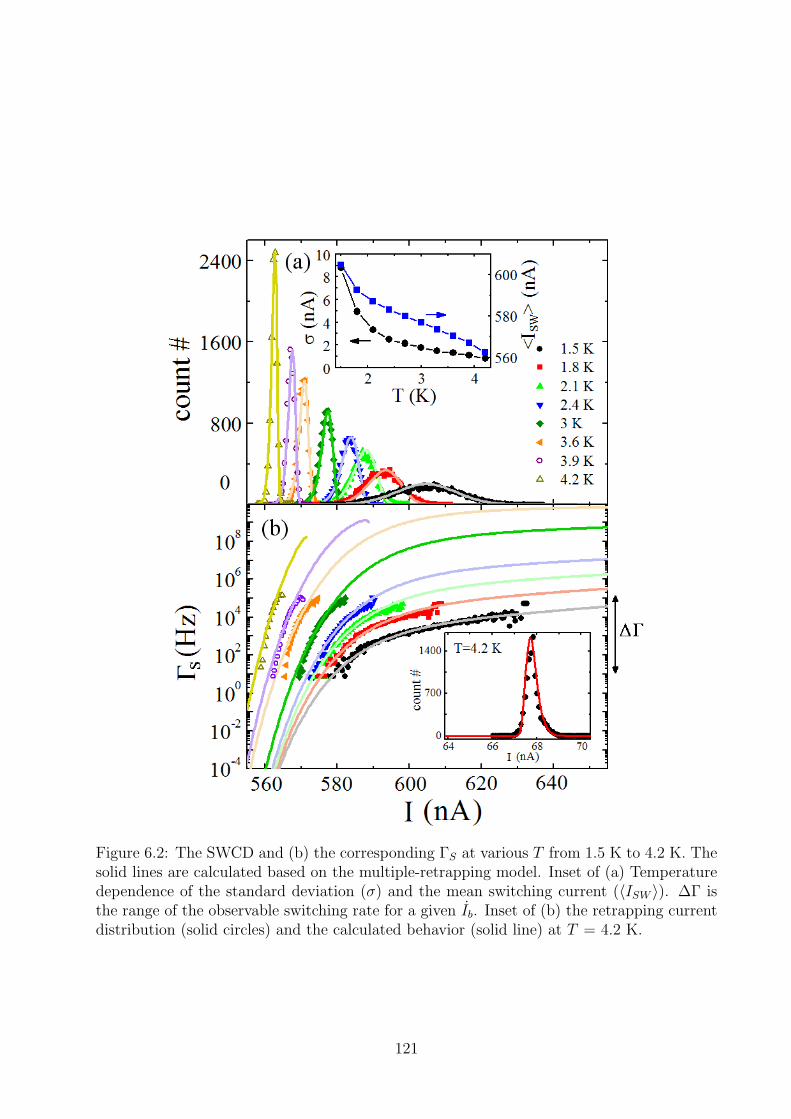
Figure 6.2: The SWCD and (b) the corresponding ΓS at various T from 1.5 K to 4.2 K. Thesolid lines are calculated based on the multiple-retrapping model. Inset of (a) Temperaturedependence of the standard deviation (σ) and the mean switching current (〈ISW 〉). ∆Γ isthe range of the observable switching rate for a given Ib. Inset of (b) the retrapping currentdistribution (solid circles) and the calculated behavior (solid line) at T = 4.2 K.
121
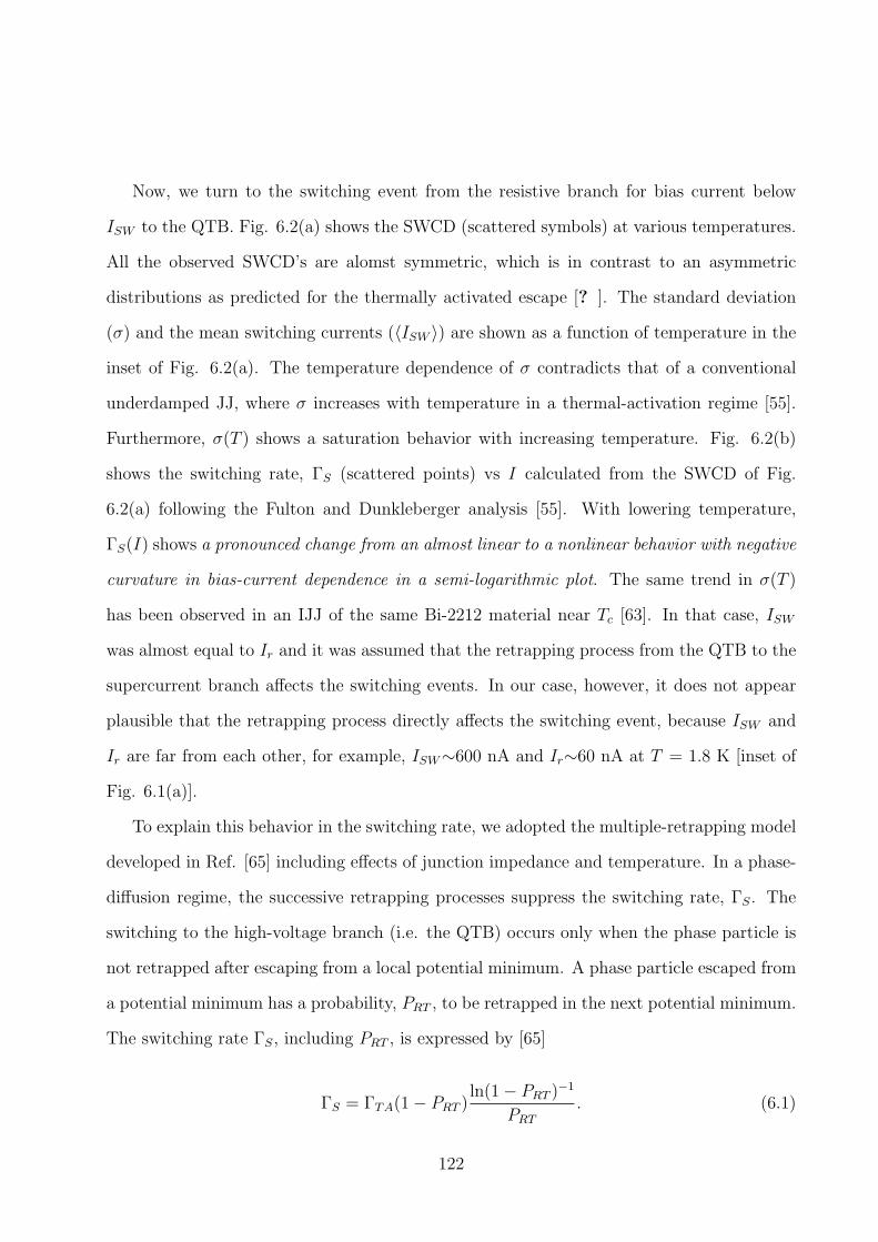
Now, we turn to the switching event from the resistive branch for bias current below
ISW to the QTB. Fig. 6.2(a) shows the SWCD (scattered symbols) at various temperatures.
All the observed SWCD’s are alomst symmetric, which is in contrast to an asymmetric
distributions as predicted for the thermally activated escape [? ]. The standard deviation
(σ) and the mean switching currents (〈ISW 〉) are shown as a function of temperature in the
inset of Fig. 6.2(a). The temperature dependence of σ contradicts that of a conventional
underdamped JJ, where σ increases with temperature in a thermal-activation regime [55].
Furthermore, σ(T ) shows a saturation behavior with increasing temperature. Fig. 6.2(b)
shows the switching rate, ΓS (scattered points) vs I calculated from the SWCD of Fig.
6.2(a) following the Fulton and Dunkleberger analysis [55]. With lowering temperature,
ΓS(I) shows a pronounced change from an almost linear to a nonlinear behavior with negative
curvature in bias-current dependence in a semi-logarithmic plot. The same trend in σ(T )
has been observed in an IJJ of the same Bi-2212 material near Tc [63]. In that case, ISW
was almost equal to Ir and it was assumed that the retrapping process from the QTB to the
supercurrent branch affects the switching events. In our case, however, it does not appear
plausible that the retrapping process directly affects the switching event, because ISW and
Ir are far from each other, for example, ISW∼600 nA and Ir∼60 nA at T = 1.8 K [inset of
Fig. 6.1(a)].
To explain this behavior in the switching rate, we adopted the multiple-retrapping model
developed in Ref. [65] including effects of junction impedance and temperature. In a phase-
diffusion regime, the successive retrapping processes suppress the switching rate, ΓS. The
switching to the high-voltage branch (i.e. the QTB) occurs only when the phase particle is
not retrapped after escaping from a local potential minimum. A phase particle escaped from
a potential minimum has a probability, PRT , to be retrapped in the next potential minimum.
The switching rate ΓS, including PRT , is expressed by [65]
ΓS = ΓTA(1 − PRT )ln(1 − PRT )−1
PRT
. (6.1)
122
Here, ΓTA = ωp
2πexp(- ∆U
kBT) is the thermally activated escape rate, ωp = ωp0(1-γ2)1/4, ωp0 =
(2eIc/~C)1/2, ∆U(φ)[ = 2EJ((1-γ2)1/2-γarccosγ)] is the escape energy barrier, and γ[ = I/Ic]
is a normalized bias current. The retrapping probability can be obtained by an integration
(see Ref. [72]) of the retrapping rate
ΓRT =1
ZJC(∆URT/πkBT )1/2exp(−∆URT/kBT ) (6.2)
where ∆URT (I) = Z2JC(I-Ir0)
2 and Ir0 is the noise-free return current from a QTB to a PDB
[73]. Here, ZJ is the fitting parameter representing the total shunt impedance.
Fig. 6.3(a) shows an experimental switching distribution from Fig. 6.2(a) (red dots) at
T = 1.5 K with the corresponding fit (blue curve) obtained by using Eq. 6.1 with the best-fit
parameters of ZJ = 61.9 Ω, Ic = 1.26 µA, and Ir0 = 63 nA. The junction capacitance, 330
fF, was estimated from the typical value of 45 fF/µm2 for Bi-2212 IJJ’s. The corresponding
switching rate (red dots) and the fit (blue curve) are shown in Fig. 6.3(b), with the same
parameters. An excellent agreement is obtained in both fittings.
These results are analyzed in terms of ZJ - and T -dependence of PRT . The inset of Fig.
6.3(a) shows the calculated PRT vs I curves for various ZJ at T = 1.5 K, with the values of Ic
and Ir0 obtained from the best fits shown in Fig. 6.3. The retrapping-probability curve shifts
to higher currents as ZJ decreases, due to the ZJ dependence of ∆URT in the exponential
factor of ΓRT . The bias-current positions of almost vanishing PRT , indicated by downward
arrows, approximately correspond to the maximum current allowing the retrapping. We
denote this current as IPD. Physically this is the same current as the one denoted Im in
Ref. [66]. The system can hardly be retrapped at a current higher than IPD, because in this
case the energy fed to the system by the bias current gets larger than the dissipated energy.
By equating the energy fed and the energy dissipated, similar to McCumber and Stewart
123
Figure 6.3: (a) The solid lines represent the calculated SWCD’s for various ZJ values of 106Ω, 61.9 Ω, 50 Ω, and 40 Ω, corresponding to QPD = 3.88, 2.37, 1.90 and 1.55, respectively.Red dots show the SWCD at T = 1.5 K. Inset: Theoretical retrapping probabilities versusbias current, for various ZJ values at T = 1.5 K. The downward arrows indicate the IPD
values. (b) Estimated switching rate versus the bias current. Red dots correspond to theexperimental switching rate for T = 1.5 K. Estimated ΓS for various ZJ values in Eq. 6.1 areshown as solid lines. Inset: Estimated retrapping probabilities versus bias current with ZJ =61.9 Ω at various T . Thick black curves in (a) and (b) show the thermally activated SWCDand the corresponding escape rate, respectively, without multiple retrapping processes.
analysis [66, 62], one obtains the relation
IPD = 4Ic/πQPD, (6.3)
whereQPD is the phase-diffusion quality factor at ω∼ωp. In fact, the noise-free retrapping
124
current can be written in a form similar to Eq. 6.3, namely as Ir0 = 4Ic/πQ(ω = 0) [30]. The
thick black curves in Figs. 6.3(a) and 6.3(b) show theoretical SWCD and the corresponding
ΓTA(I), respectively, predicted by the thermal activation model. Other solid curves in Fig.
6.3(b) are ΓS(I) (Eq. 6.1) for varying ZJ under the multiple retrapping processes. ΓS(I)
with each ZJ in Fig. 6.3(b) starts to drop quickly from ΓTA(I) at I = IPD, which are denoted
by arrows in the figure. We define IPD as the bias-current value corresponding to PRT =
0.01, where ΓS(IPD) is nearly the same as the ΓTA(IPD) as shown in Fig. 6.3(b) [65]. The
impedance of 106 Ω gives the same SWCD as thermally activated SWCD without retrapping
because ΓS(I) overlaps with ΓTA(I) in the observable switching rate window, ∆Γ (between
the two horizontal dashed lines in Fig. 6.3(b)), although ZJ is of the order of ZL. When
ΓS (IPD) start to deviate from the ΓTA in ∆Γ while ZJ keeps decreasing, the retrapping
phenomenon, which is due to the high-frequency dissipation, begins to influence the SCDW.
The observable window of ∆Γ for a fixed I shifts to the steeper section with decreasing ZJ
or increasing IPD. This gives a decrease of the SWCD width at a constant temperature (Fig.
6.3(a)). We also note that as ZJ becomes smaller, IPD becomes larger and correspondingly,
according to Eq. 6.3, QPD becomes smaller. Thus, we conclude that the distribution width
becomes smaller if the quality factor is reduced.
Since IPD is also affected by temperature, the shape of ΓS(I) also depends on tempera-
ture. The inset of Fig. 6.3(b) illustrates PRT vs I at various temperatures. Here, ZJ is fixed
at 61.9 Ω and other parameters, except for T , are set to be the same as for the inset of Fig.
6.3(a). The bias-current position of the zero-temperature curve, indicated by an upward
arrow in the inset of Fig. 6.3(b), corresponds to the fluctuation-free return current Ir0. The
value of IPD shown by arrows increases with increasing temperature. Thus, in effect, the
retrapping probability curve shifts to higher currents as temperature is raised as shown in
the inset of Fig. 6.3(b), due to the presence of a Boltzmann-type exponential factor in the
expression of ΓRT . To explain the observed SWCD and the corresponding switching rate
at different temperatures, therefore, one should consider both effects of the junction shunt
125
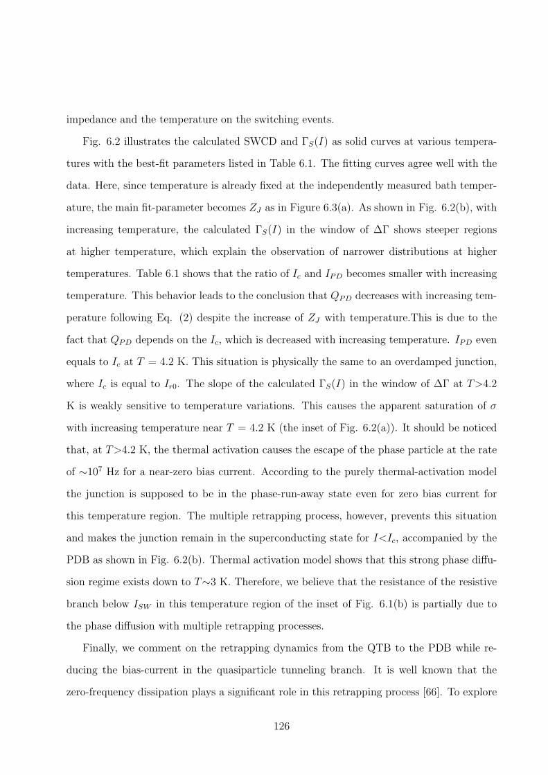
impedance and the temperature on the switching events.
Fig. 6.2 illustrates the calculated SWCD and ΓS(I) as solid curves at various tempera-
tures with the best-fit parameters listed in Table 6.1. The fitting curves agree well with the
data. Here, since temperature is already fixed at the independently measured bath temper-
ature, the main fit-parameter becomes ZJ as in Figure 6.3(a). As shown in Fig. 6.2(b), with
increasing temperature, the calculated ΓS(I) in the window of ∆Γ shows steeper regions
at higher temperature, which explain the observation of narrower distributions at higher
temperatures. Table 6.1 shows that the ratio of Ic and IPD becomes smaller with increasing
temperature. This behavior leads to the conclusion that QPD decreases with increasing tem-
perature following Eq. (2) despite the increase of ZJ with temperature.This is due to the
fact that QPD depends on the Ic, which is decreased with increasing temperature. IPD even
equals to Ic at T = 4.2 K. This situation is physically the same to an overdamped junction,
where Ic is equal to Ir0. The slope of the calculated ΓS(I) in the window of ∆Γ at T>4.2
K is weakly sensitive to temperature variations. This causes the apparent saturation of σ
with increasing temperature near T = 4.2 K (the inset of Fig. 6.2(a)). It should be noticed
that, at T>4.2 K, the thermal activation causes the escape of the phase particle at the rate
of ∼107 Hz for a near-zero bias current. According to the purely thermal-activation model
the junction is supposed to be in the phase-run-away state even for zero bias current for
this temperature region. The multiple retrapping process, however, prevents this situation
and makes the junction remain in the superconducting state for I<Ic, accompanied by the
PDB as shown in Fig. 6.2(b). Thermal activation model shows that this strong phase diffu-
sion regime exists down to T∼3 K. Therefore, we believe that the resistance of the resistive
branch below ISW in this temperature region of the inset of Fig. 6.1(b) is partially due to
the phase diffusion with multiple retrapping processes.
Finally, we comment on the retrapping dynamics from the QTB to the PDB while re-
ducing the bias-current in the quasiparticle tunneling branch. It is well known that the
zero-frequency dissipation plays a significant role in this retrapping process [66]. To explore
126
T (K) Ic(µA) Ir0(nA) ZJ(Ω) IPD (nA) QPD
1.5 1.263 63.00 61.9 678 2.372.4 1.209 65.10 77.6 683 2.253.0 1.006 63.44 86.0 685 1.873.6 0.735 65.22 94.7 682 1.374.2 0.572 63.79 101.5 572 1.27
Table 6.1: Fitting parameters for the switching events for selected temperatures
this zero-frequency damping effect on this system, we obtained the retrapping current dis-
tribution from the QTB-PDB switching at T = 4.2 K. The inset of Fig. 6.1(b) shows the
stochastic nature of the retrapping current as shown by solid circles at T = 4.2 K. The shape
of the current distribution shows an asymmetry, i.e., the current region lower than the mean
value gives sharper distribution because the noise-free Ir0 is a lower bound for the distribu-
tion. [64]. The calculated retrapping distribution (solid line) by the retrapping rate, ΓRT ,
is consistent with the experimental result. The best-fit parameters are Ir0 = 63.8 nA and
ZJ = 10 kΩ (∼Rqp), where the estimated noise-free Ir0 matches with the value used for ΓS
fitting. The values of Ir0 for various temperatures are listed in Table I. The junction shunt
impedance ZJ estimated from the return currents is significantly larger than that found for
the switching events. It indicates that the retrapping phenomena from QTB to PDB are
mainly determined by a low-frequency limit damping with Q(ω∼0) = 11.4 with Ic = 572 nA
and Ir0 = 63.8 nA at T = 4.2 K as shown in Table 6.1.
6.4 Summary
In this report, we study high-Tc IJJ’s, which have suppressed critical currents due to FIB
treatment. We show that the multiple-retrapping processes in a hysteretic IJJ with a high
tunneling resistance govern the switching from a resistive state in phase-diffusion regime into
the quasiparticle tunneling state. The predicted SWCD and ΓS in the multiple-retrapping
model are in good agreement with the observed broadening of the distribution of switching
127
currents with decreasing temperature. We also demonstrate that the change of the shapes of
the observed SWCD and ΓS in various temperatures can be understood by the junction shunt
impedance and temperature dependence of the retrapping rate, in terms of junction quality
factor in the phase diffusion regime. As the macroscopic quantum tunneling has recently
been observed in IJJ’s of Bi-2212 single crystals [7], this study provides useful information
about the dissipative environment.
128
Appendix A
MQT in high-TC intrinsic Josephson
junctions
In order to verify that we can observe MQT in our 3He setup, we measured two high-TC
crystal samples with intrinsic Josephson junctions (IJJ), using the same measurement scheme
that was used for the nanowire sample measurements. The general idea in doing this was
that the MQT in high-TC stacked junctions is well known and well understood. By observing
the results seen by other groups we hope to gain extra confidence in the correctness of our
setup. Indeed, the results obtained in such test confirm that the setup is working properly,
as is explained in more details below.
Fig. A.1 shows the standard deviation of the switching current distributions as a function
of temperature obtained from the two samples, IJJ1 and IJJ2. The samples were fabricated
from Bi2Sr2CaCu2O8+x crystal shaped using focused ion beam (FIB) to the lateral dimen-
sions of 1.6 2.4 µm2 (IJJ1). The bias current in these measurements was injected parallel to
the c-axis (i.e., perpendicular to the weakly coupled superconducting planes of the crystal).
In Fig. A.1, we observe a crossover from a thermal activated escape regime to MQT regime
near T ∗ = 0.65 K for IJJ1 and near T ∗ = 0.35 K for IJJ2, which is manifested by a saturation
behavior of the standard deviation at lowering temperatures [7]. We also find that, in the
high temperature range, σ is proportional to T 2/3 which is expected for a thermally activated
escape model [6]. To validate this further, we estimated the escape temperature, Tesc , from
the escape rates, (obtained from switching current distributions) at different temperatures
(see Fig. A.2). For this, we used the usual expression,
Γ = (ωp/2π) exp(−∆U/kBTesc) (A.1)
129
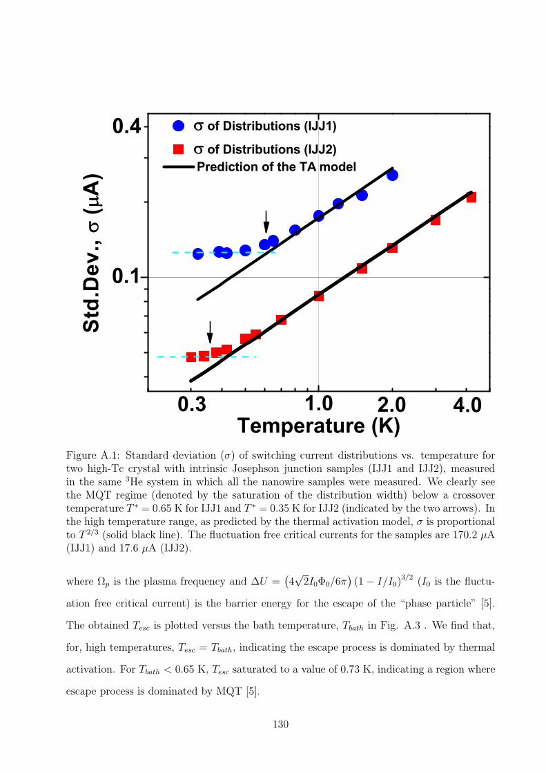
1.0
0.1
0.4
4.0
of Distributions (IJJ1)
of Distributions (IJJ2) Prediction of the TA model
2.0
S
td.D
ev.,
(A
)
Temperature (K)0.3
Figure A.1: Standard deviation (σ) of switching current distributions vs. temperature fortwo high-Tc crystal with intrinsic Josephson junction samples (IJJ1 and IJJ2), measuredin the same 3He system in which all the nanowire samples were measured. We clearly seethe MQT regime (denoted by the saturation of the distribution width) below a crossovertemperature T ∗ = 0.65 K for IJJ1 and T ∗ = 0.35 K for IJJ2 (indicated by the two arrows). Inthe high temperature range, as predicted by the thermal activation model, σ is proportionalto T 2/3 (solid black line). The fluctuation free critical currents for the samples are 170.2 µA(IJJ1) and 17.6 µA (IJJ2).
where Ωp is the plasma frequency and ∆U =(4√
2I0Φ0/6π)(1 − I/I0)
3/2 (I0 is the fluctu-
ation free critical current) is the barrier energy for the escape of the “phase particle” [5].
The obtained Tesc is plotted versus the bath temperature, Tbath in Fig. A.3 . We find that,
for, high temperatures, Tesc = Tbath, indicating the escape process is dominated by thermal
activation. For Tbath < 0.65 K, Tesc saturated to a value of 0.73 K, indicating a region where
escape process is dominated by MQT [5].
130
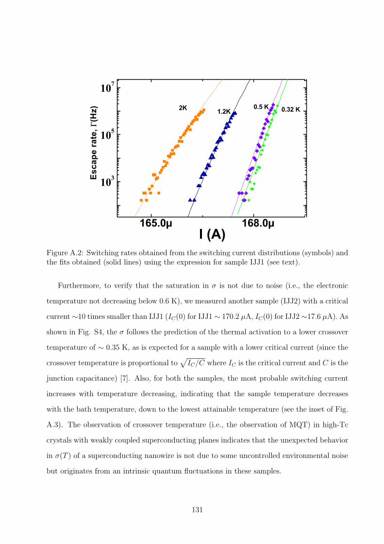
165.0µ 168.0µ
103
105
107
0.32 K0.5 K1.2K2K
Esca
pe ra
te,
(Hz)
I (A)Figure A.2: Switching rates obtained from the switching current distributions (symbols) andthe fits obtained (solid lines) using the expression for sample IJJ1 (see text).
Furthermore, to verify that the saturation in σ is not due to noise (i.e., the electronic
temperature not decreasing below 0.6 K), we measured another sample (IJJ2) with a critical
current ∼10 times smaller than IJJ1 (IC(0) for IJJ1 ∼ 170.2 µA, IC(0) for IJJ2 ∼17.6 µA). As
shown in Fig. S4, the σ follows the prediction of the thermal activation to a lower crossover
temperature of ∼ 0.35 K, as is expected for a sample with a lower critical current (since the
crossover temperature is proportional to√IC/C where IC is the critical current and C is the
junction capacitance) [7]. Also, for both the samples, the most probable switching current
increases with temperature decreasing, indicating that the sample temperature decreases
with the bath temperature, down to the lowest attainable temperature (see the inset of Fig.
A.3). The observation of crossover temperature (i.e., the observation of MQT) in high-Tc
crystals with weakly coupled superconducting planes indicates that the unexpected behavior
in σ(T ) of a superconducting nanowire is not due to some uncontrolled environmental noise
but originates from an intrinsic quantum fluctuations in these samples.
131
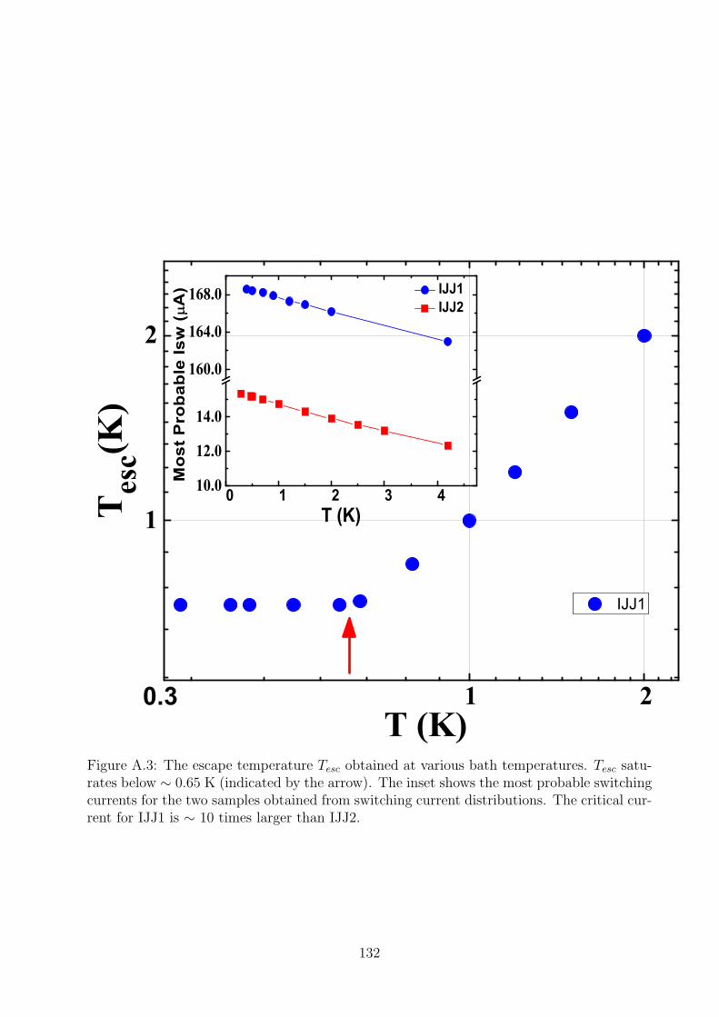
1 2
1
2
IJJ1
Tesc(K)
T (K)0.3
0 1 2 3 410.0
12.0
14.0
160.0
164.0
168.0
IJJ1 IJJ2
Mo
st P
rob
able
Isw
(A
)
T (K)
Figure A.3: The escape temperature Tesc obtained at various bath temperatures. Tesc satu-rates below ∼ 0.65 K (indicated by the arrow). The inset shows the most probable switchingcurrents for the two samples obtained from switching current distributions. The critical cur-rent for IJJ1 is ∼ 10 times larger than IJJ2.
132
References
[1] AO Caldeira and AJ Leggett. Influence of dissipation on quantum tunneling in macro-scopic systems. Physical Review Letters, 46(4):211–214, 1981.
[2] A. J. Leggett, S. Chakravarty, A. T. Dorsey, Matthew P. A. Fisher, Anupam Garg, andW. Zwerger. Dynamics of the dissipative two-state system. Rev. Mod. Phys., 59(1):1–85,Jan 1987.
[3] S. Takagi. Macroscopic quantum tunneling. Cambridge University Press, 2002.
[4] Richard F. Voss and Richard A. Webb. Macroscopic Quantum Tunneling in 1-µm NbJosephson Junctions. Phys. Rev. Lett., 47(4):265–268, Jul 1981.
[5] J.M. Martinis, M.H. Devoret, and J. Clarke. Experimental tests for the quantum be-havior of a macroscopic degree of freedom: The phase difference across a Josephsonjunction. Physical Review B, 35(10):4682–4698, 1987.
[6] A. Wallraff, A. Lukashenko, J. Lisenfeld, A. Kemp, MV Fistul, Y. Koval, and AV Usti-nov. Quantum dynamics of a single vortex. Nature, 425(6954):155–158, 2003.
[7] K. Inomata, S. Sato, K. Nakajima, A. Tanaka, Y. Takano, HB Wang, M. Nagao,H. Hatano, and S. Kawabata. Macroscopic quantum tunneling in a d-wave high-TCBi2Sr2CaCu2O8+ delta superconductor. Phys Rev Lett, 95(10):107005, 2005.
[8] W. Wernsdorfer, EB Orozco, K. Hasselbach, A. Benoit, D. Mailly, O. Kubo, H. Nakano,and B. Barbara. Macroscopic quantum tunneling of magnetization of single ferrimag-netic nanoparticles of barium ferrite. Physical Review Letters, 79(20):4014–4017, 1997.
[9] JE Mooij and C. Harmans. Phase-slip flux qubits. New Journal of Physics, 7(1):219,2005.
[10] N. Giordano and E. R. Schuler. Macroscopic quantum tunneling and related effects ina one-dimensional superconductor. Phys. Rev. Lett., 63(21):2417–2420, Nov 1989.
[11] W.A. Little. Decay of persistent currents in small superconductors. Physical Review,156(2):396–403, 1967.
[12] JE Mooij and Y.V. Nazarov. Superconducting nanowires as quantum phase-slip junc-tions. Nature Physics, 2(3):169–172, 2006.
133
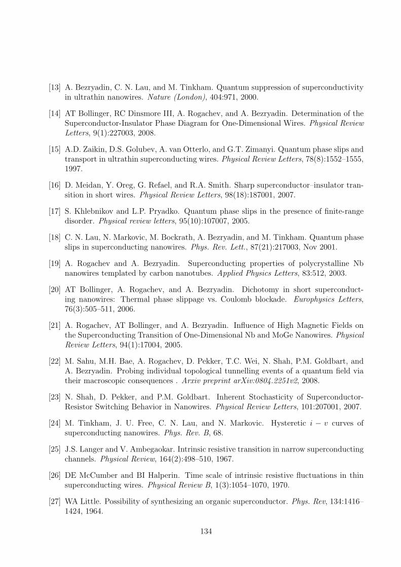
[13] A. Bezryadin, C. N. Lau, and M. Tinkham. Quantum suppression of superconductivityin ultrathin nanowires. Nature (London), 404:971, 2000.
[14] AT Bollinger, RC Dinsmore III, A. Rogachev, and A. Bezryadin. Determination of theSuperconductor-Insulator Phase Diagram for One-Dimensional Wires. Physical ReviewLetters, 9(1):227003, 2008.
[15] A.D. Zaikin, D.S. Golubev, A. van Otterlo, and G.T. Zimanyi. Quantum phase slips andtransport in ultrathin superconducting wires. Physical Review Letters, 78(8):1552–1555,1997.
[16] D. Meidan, Y. Oreg, G. Refael, and R.A. Smith. Sharp superconductor–insulator tran-sition in short wires. Physical Review Letters, 98(18):187001, 2007.
[17] S. Khlebnikov and L.P. Pryadko. Quantum phase slips in the presence of finite-rangedisorder. Physical review letters, 95(10):107007, 2005.
[18] C. N. Lau, N. Markovic, M. Bockrath, A. Bezryadin, and M. Tinkham. Quantum phaseslips in superconducting nanowires. Phys. Rev. Lett., 87(21):217003, Nov 2001.
[19] A. Rogachev and A. Bezryadin. Superconducting properties of polycrystalline Nbnanowires templated by carbon nanotubes. Applied Physics Letters, 83:512, 2003.
[20] AT Bollinger, A. Rogachev, and A. Bezryadin. Dichotomy in short superconduct-ing nanowires: Thermal phase slippage vs. Coulomb blockade. Europhysics Letters,76(3):505–511, 2006.
[21] A. Rogachev, AT Bollinger, and A. Bezryadin. Influence of High Magnetic Fields onthe Superconducting Transition of One-Dimensional Nb and MoGe Nanowires. PhysicalReview Letters, 94(1):17004, 2005.
[22] M. Sahu, M.H. Bae, A. Rogachev, D. Pekker, T.C. Wei, N. Shah, P.M. Goldbart, andA. Bezryadin. Probing individual topological tunnelling events of a quantum field viatheir macroscopic consequences . Arxiv preprint arXiv:0804.2251v2, 2008.
[23] N. Shah, D. Pekker, and P.M. Goldbart. Inherent Stochasticity of Superconductor-Resistor Switching Behavior in Nanowires. Physical Review Letters, 101:207001, 2007.
[24] M. Tinkham, J. U. Free, C. N. Lau, and N. Markovic. Hysteretic i − v curves ofsuperconducting nanowires. Phys. Rev. B, 68.
[25] J.S. Langer and V. Ambegaokar. Intrinsic resistive transition in narrow superconductingchannels. Physical Review, 164(2):498–510, 1967.
[26] DE McCumber and BI Halperin. Time scale of intrinsic resistive fluctuations in thinsuperconducting wires. Physical Review B, 1(3):1054–1070, 1970.
[27] WA Little. Possibility of synthesizing an organic superconductor. Phys. Rev, 134:1416–1424, 1964.
134
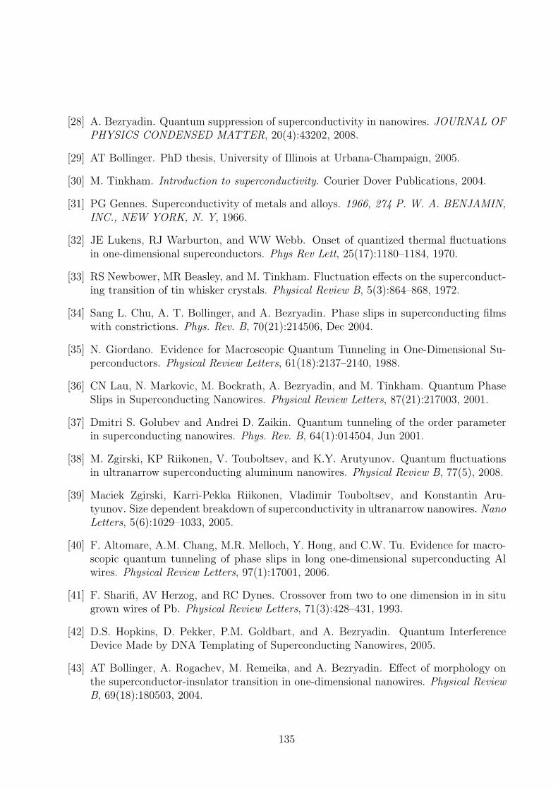
[28] A. Bezryadin. Quantum suppression of superconductivity in nanowires. JOURNAL OFPHYSICS CONDENSED MATTER, 20(4):43202, 2008.
[29] AT Bollinger. PhD thesis, University of Illinois at Urbana-Champaign, 2005.
[30] M. Tinkham. Introduction to superconductivity. Courier Dover Publications, 2004.
[31] PG Gennes. Superconductivity of metals and alloys. 1966, 274 P. W. A. BENJAMIN,INC., NEW YORK, N. Y, 1966.
[32] JE Lukens, RJ Warburton, and WW Webb. Onset of quantized thermal fluctuationsin one-dimensional superconductors. Phys Rev Lett, 25(17):1180–1184, 1970.
[33] RS Newbower, MR Beasley, and M. Tinkham. Fluctuation effects on the superconduct-ing transition of tin whisker crystals. Physical Review B, 5(3):864–868, 1972.
[34] Sang L. Chu, A. T. Bollinger, and A. Bezryadin. Phase slips in superconducting filmswith constrictions. Phys. Rev. B, 70(21):214506, Dec 2004.
[35] N. Giordano. Evidence for Macroscopic Quantum Tunneling in One-Dimensional Su-perconductors. Physical Review Letters, 61(18):2137–2140, 1988.
[36] CN Lau, N. Markovic, M. Bockrath, A. Bezryadin, and M. Tinkham. Quantum PhaseSlips in Superconducting Nanowires. Physical Review Letters, 87(21):217003, 2001.
[37] Dmitri S. Golubev and Andrei D. Zaikin. Quantum tunneling of the order parameterin superconducting nanowires. Phys. Rev. B, 64(1):014504, Jun 2001.
[38] M. Zgirski, KP Riikonen, V. Touboltsev, and K.Y. Arutyunov. Quantum fluctuationsin ultranarrow superconducting aluminum nanowires. Physical Review B, 77(5), 2008.
[39] Maciek Zgirski, Karri-Pekka Riikonen, Vladimir Touboltsev, and Konstantin Aru-tyunov. Size dependent breakdown of superconductivity in ultranarrow nanowires. NanoLetters, 5(6):1029–1033, 2005.
[40] F. Altomare, A.M. Chang, M.R. Melloch, Y. Hong, and C.W. Tu. Evidence for macro-scopic quantum tunneling of phase slips in long one-dimensional superconducting Alwires. Physical Review Letters, 97(1):17001, 2006.
[41] F. Sharifi, AV Herzog, and RC Dynes. Crossover from two to one dimension in in situgrown wires of Pb. Physical Review Letters, 71(3):428–431, 1993.
[42] D.S. Hopkins, D. Pekker, P.M. Goldbart, and A. Bezryadin. Quantum InterferenceDevice Made by DNA Templating of Superconducting Nanowires, 2005.
[43] AT Bollinger, A. Rogachev, M. Remeika, and A. Bezryadin. Effect of morphology onthe superconductor-insulator transition in one-dimensional nanowires. Physical ReviewB, 69(18):180503, 2004.
135
[44] KF Kelly, IW Chiang, ET Mickelson, RH Hauge, JL Margrave, X. Wang, GE Scuseria,C. Radloff, and NJ Halas. Insight into the mechanism of sidewall functionalization ofsingle-walled nanotubes: an STM study. Chemical Physics Letters, 313(3-4):445–450,1999.
[45] D.S. Hopkins, D. Pekker, T.C. Wei, P.M. Goldbart, and A. Bezryadin. Local superfluiddensities probed via current-induced superconducting phase gradients. Physical ReviewB, 76(22):220506, 2007.
[46] A. Johansson, G. Sambandamurthy, D. Shahar, N. Jacobson, and R. Tenne. NanowireActing as a Superconducting Quantum Interference Device. Physical Review Letters,95(11):116805, 2005.
[47] Y. Zhang and H. Dai. Formation of metal nanowires on suspended single-walled carbonnanotubes. Applied Physics Letters, 77:3015, 2000.
[48] ET Mickelson, CB Huffman, AG Rinzler, RE Smalley, RH Hauge, and JL Margrave.Fluorination of single-wall carbon nanotubes. Chemical Physics Letters, 296(1-2):188–194, 1998.
[49] A. Rogachev, T.C. Wei, D. Pekker, AT Bollinger, PM Goldbart, and A. Bezryadin.Magnetic-Field Enhancement of Superconductivity in Ultranarrow Wires. Physical Re-view Letters, 97(13):137001, 2006.
[50] JM Graybeal and MR Beasley. Localization and interaction effects in ultrathin amor-phous superconducting films. Physical Review B, 29(7):4167–4169, 1984.
[51] JM Graybeal. PhD thesis, Stanford University, 1985.
[52] UC Coskun. PhD thesis, University of Illinois at Urbana-Champaign, 2005.
[53] B. Muhlschlegel. Die thermodynamischen funktionen des supraleiters. Zeitschrift furPhysik A Hadrons and Nuclei, 155(3):313–327, 1959.
[54] W.J. Skocpol, M.R. Beasley, and M. Tinkham. Self-heating hotspots in superconductingthin-film microbridges. Journal of Applied, 45:4054, 1974.
[55] T. A. Fulton and L. N. Dunkleberger. Lifetime of the zero-voltage state in josephsontunnel junctions. Phys. Rev. B, 9(11):4760–4768, Jun 1974.
[56] KK Likharev. Superconducting weak links. Reviews of Modern Physics, 51(1):101–161,1979.
[57] J. Bardeen. Critical fields and currents in superconductors. Reviews of Modern Physics,34(4):667–681, 1962.
[58] M. Tinkham and CN Lau. Quantum limit to phase coherence in thin superconductingwires. Applied Physics Letters, 80:2946, 2002.
136
[59] NB Kopnin. Theory of nonequilibrium superconductivity. Oxford University Press, 2001.
[60] P. Hanggi, P. Talkner, and M. Borkovec. Reaction rate theory: fifty years after KramersRev. Mod. Phys, 62:251–342, 1990.
[61] D. Vion, M. Gotz, P. Joyez, D. Esteve, and M. H. Devoret. Thermal activationabove a dissipation barrier: Switching of a small josephson junction. Phys. Rev. Lett.,77(16):3435–3438, Oct 1996.
[62] JM Kivioja, TE Nieminen, J. Claudon, O. Buisson, FW Hekking, and JP Pekola.Observation of transition from escape dynamics to underdamped phase diffusion in aJosephson junction. Physical Review Letters, 94(24):247002, 2005.
[63] V. M. Krasnov, T. Bauch, S. Intiso, E. Hurfeld, T. Akazaki, H. Takayanagi, and P. Dels-ing. Collapse of thermal activation in moderately damped josephson junctions. Phys.Rev. Lett., 95(15):157002, Oct 2005.
[64] JC Fenton and PA Warburton. Monte Carlo simulations of thermal fluctuations inmoderately damped Josephson junctions: Multiple escape and retrapping, switching-and return current distributions, and hysteresis. Physica C Phys Rev B, 78(462):054526,2008.
[65] J. Mannik, S. Li, W. Qiu, W. Chen, V. Patel, S. Han, and JE Lukens. Crossoverfrom Kramers to phase-diffusion switching in moderately damped Josephson junctions(4 pages). PHYSICAL REVIEW-SERIES B-, 71(22):220509, 2005.
[66] John M. Martinis and R. L. Kautz. Classical phase diffusion in small hysteretic joseph-son junctions. Phys. Rev. Lett., 63(14):1507–1510, Oct 1989.
[67] A. T. Johnson, C. J. Lobb, and M. Tinkham. Effect of leads and energy gap uponthe retrapping current of josephson junctions. Phys. Rev. Lett., 65(10):1263–1266, Sep1990.
[68] A. Franz, Y. Koval, D. Vasyukov, P. Muller, H. Schneidewind, D. A. Ryndyk, J. Keller,and C. Helm. Thermal fluctuations in ultrasmall intrinsic josephson junctions. Phys.Rev. B, 69(1):014506, Jan 2004.
[69] P. A. Warburton, A. R. Kuzhakhmetov, G. Burnell, M. G. Blamire, and H. Schnei-dewind. Decoupling of a current-biased intrinsic josephson junction from its environ-ment. Phys. Rev. B, 67(18):184513, May 2003.
[70] S.J. Kim, Y.I. Latyshev, and T. Yamashita. Submicron stacked-junction fabrica-tion from BiSrCaCuO whiskers by focused-ion-beam etching. Applied Physics Letters,74:1156, 1999.
[71] N. Kim, Y.J. Doh, H.S. Chang, and H.J. Lee. Suppressed superconductivity of thesurface conduction layer in Bi 2 Sr 2 CaCu 2 O 8 single crystals probed by c-axistunneling measurements. Phys Rev B, 59:14639, 1999.
137
[72] Anupam Garg. Escape-field distribution for escape from a metastable potential wellsubject to a steadily increasing bias field. Phys. Rev. B, 51(21):15592–15595, Jun 1995.
[73] E. Ben-Jacob, D. J. Bergman, B. J. Matkowsky, and Z. Schuss. Lifetime of oscillatorysteady states. Phys. Rev. A, 26(5):2805–2816, Nov 1982.
138

Author’s Biography
Mitrabhanu Sahu was born on June 7th 1980 in Cuttack, India. He graduated from the Indian
Institute of Technology, Kharagpur in April of 2003 with a B.Sc. majoring in Physics. He
spent the summer of 2002 at the Indian Institute of Science, Bangalore as an intern where he
studied surface defect characterization of Si/Si02 through wet etching and optical imaging.
He was awarded a gold medal as one of the top five physics students in an all India level
examination conducted by the India Physics Teachers’ Association in 2002.
In the fall of 2003 Mitrabhanu enrolled at the University of Illinois at Urbana-Champaign
to begin his doctoral studies. Being always fascinated by low-temperature Physics, and
especially nano-devices he joined the group of his advisor, Alexey Bezryadin in January
of 2004. In the Bezryadin group, he learned to fabricate superconducting nanowires using
single walled carbon nanotubes as templates. He used these wires to study the effects of
quantum fluctuations quasi -one-dimensional systems. From his measurements of switching
current distributions, previously unexplored in nanowires, evidence for quantum phase slips
in nanowires was found. Most importantly it was found that at low enough temperatures
every quantum phase slip causes switching in the wire from the superconducting state to
the resistive state. After completion of his Ph.D, Mitrabhanu will begin his work for Intel
Corporation as Process Technology Development Engineer.
139