Embed Size (px)
Citation preview

This is the author’s version of a work that was submitted/accepted for pub-lication in the following source:
Coetzee, Jacob, Cordwell, James, Underwood, Elizabeth, & Waite,Shauna(2011)Single-layer decoupling networks for circulant symmetric arrays.IETE Technical Review, 28(3), pp. 232-239.
This file was downloaded from: https://eprints.qut.edu.au/43619/
c© Copyright 2011 Institution of Electronics and TelecommunicationEngineers (IETE)
Notice: Changes introduced as a result of publishing processes such ascopy-editing and formatting may not be reflected in this document. For adefinitive version of this work, please refer to the published source:
https://doi.org/10.4103/0256-4602.81235

IET
E T
ech
nic
al R
evie
w • V
olu
me 2
8 • Issu
e 2
• Marc
h-A
pril 2
011
• Pages 8
7-1
92
ISSN : 0256-4602
www.ietejournals.org
Subscriber Copy : Not for Resale
IETE TELECOMMUNICATION
ENGINEERS
TH
E IN
STIT
UTIO
N O
F
ELE
CTR
ON
ICS
AN
D
The Institution of Electronics and Telecommunication Engineers
Technical ReviewIETE
Volume 28 No. 3 May-Jun 2011
232 IETE TECHNICAL REVIEW | VOL 28 | ISSUE 3 | MAY-JUN 2011
Single-layer Decoupling Networks for Circulant Symmetric Arrays
Jacob C. Coetzee, James D. Cordwell, Elizabeth Underwood and Shauna L. WaiteSchool of Engineering Systems, Queensland University of Technology, GPO Box 2434, Brisbane QLD 4001, Australia
Abstract
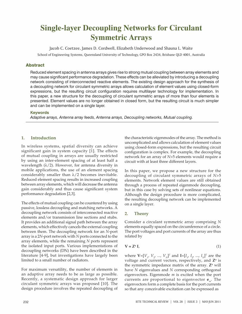
Reduced element spacing in antenna arrays gives rise to strong mutual coupling between array elements and may cause significant performance degradation. These effects can be alleviated by introducing a decoupling network consisting of interconnected reactive elements. The existing design approach for the synthesis of a decoupling network for circulant symmetric arrays allows calculation of element values using closed-form expressions, but the resulting circuit configuration requires multilayer technology for implementation. In this paper, a new structure for the decoupling of circulant symmetric arrays of more than four elements is presented. Element values are no longer obtained in closed form, but the resulting circuit is much simpler and can be implemented on a single layer.
KeywordsAdaptive arrays, Antenna array feeds, Antenna arrays, Decoupling networks, Mutual coupling.
1. Introduction
In wireless systems, spatial diversity can achieve significant gain in system capacity [1]. The effects of mutual coupling in arrays are usually restricted by using an inter-element spacing of at least half a wavelength (λ/2). However, for antenna diversity in mobile applications, the use of an element spacing considerably smaller than λ/2 becomes inevitable. Reduced element spacing results in increased coupling between array elements, which will decrease the antenna gain considerably and thus cause significant system performance degradation [2,3].
The effects of mutual coupling can be countered by using passive, lossless decoupling and matching networks. A decoupling network consists of interconnected reactive elements and/or transmission line sections and stubs. It provides an additional signal path between the array elements, which effectively cancels the external coupling between them. The decoupling network for an N-port array is a 2N-port network with N ports connected to the array elements, while the remaining N ports represent the isolated input ports. Various implementations of decoupling networks (DN) have been described in the literature [4-9], but investigations have largely been limited to a small number of radiators.
For maximum versatility, the number of elements in an adaptive array needs to be as large as possible. Recently, a systematic design approach for larger circulant symmetric arrays was proposed [10]. The design procedure involves the repeated decoupling of
the characteristic eigenmodes of the array. The method is uncomplicated and allows calculation of element values using closed-form expressions, but the resulting circuit configuration is complex. For example, the decoupling network for an array of N>5 elements would require a circuit with at least three different layers.
In this paper, we propose a new structure for the decoupling of circulant symmetric arrays of N>5 elements. Network element values are still obtained through a process of repeated eigenmode decoupling, but in this case by solving sets of nonlinear equations. Although the design procedure is more complicated, the resulting decoupling network can be implemented on a single layer.
2. Theory
Consider a circulant symmetric array comprising N elements equally spaced on the circumference of a circle. The port voltages and port currents of the array are thus related by
V = Za I, (1)
where V=[V1, V2, ..., VN]T and I=[I1, I2, ..., IN]T are the voltage and current vectors, respectively, and Za is the symmetric impedance matrix of the array. Za will have N eigenvalues and N corresponding orthogonal eigenvectors. Eigenmode m is excited when the port currents are proportional to eigenvector em. The eigenvectors form a complete basis for the port currents so that any conceivable excitation can be expressed as
233IETE TECHNICAL REVIEW | VOL 28 | ISSUE 3 | MAY-JUN 2011
I e=∑cmm
m, (2)
with cm being the excitation coefficient of mode m. Using Equation 1, the port voltages are obtained as
V Z e ea=
=∑ ∑c c Zmm
m mm
m m ,
(3)
where Zm is the eigenvalue corresponding to eigenvector em. The input impedance at port i is given by
ZVI
c Z e
c ei
i
i
mm
m mi
mm
mi
in = =∑∑
,
(4)
where emi is the ith element of em. From Equation 4, it is clear that the input impedance is dependent on the port excitations, which is a well-known consequence of mutual coupling between the array elements. When a single mode is excited, the input impedance reduces to Z Zi m
in = . The eigenvalue Zm therefore represents the input impedance observed at each port when the port currents or voltages are proportional to eigenvector em.
Decoupling of an array involves a process of modifying its impedance matrix to reduce all the off-diagonal elements to zero. An alternative approach involves a process of matching the modal input impedances. Suppose the impedance matrix of the array is modified by connecting additional circuitry to the array ports to yield a new impedance matrix Z'. If Z' has the same eigenvectors as before, but all the modal impedances are equal (i.e. Zm=Z0'), Equation 3 reduces to
V e= ′ ∑Z cmm
m0 . (5)
From Equation 4, the input impedance at each port becomes Z Zi
in = ′0 , which is independent of the port excitations. For circulant symmetric arrays, array decoupling can therefore also be accomplished by equalizing the eigenvalues of the impedance matrix of the array.
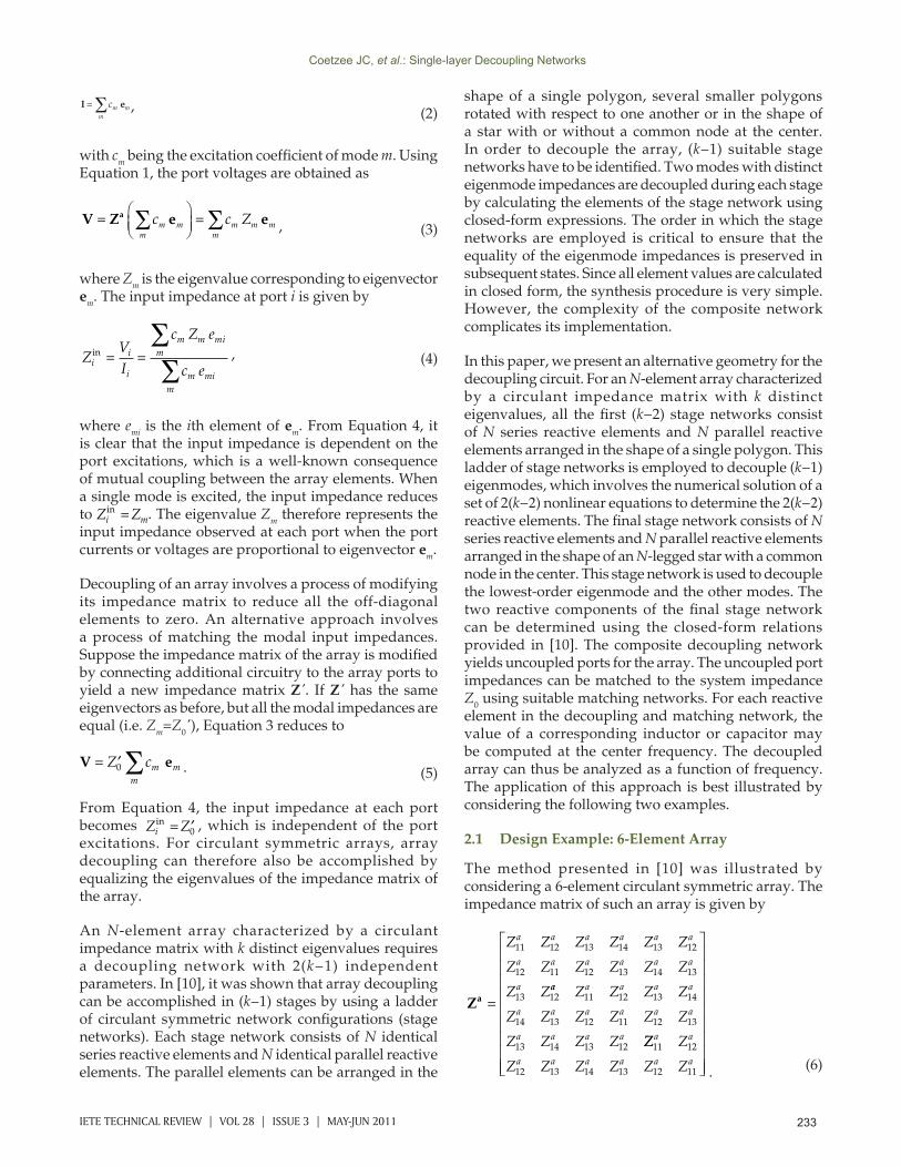
An N-element array characterized by a circulant impedance matrix with k distinct eigenvalues requires a decoupling network with 2(k−1) independent parameters. In [10], it was shown that array decoupling can be accomplished in (k−1) stages by using a ladder of circulant symmetric network configurations (stage networks). Each stage network consists of N identical series reactive elements and N identical parallel reactive elements. The parallel elements can be arranged in the
shape of a single polygon, several smaller polygons rotated with respect to one another or in the shape of a star with or without a common node at the center. In order to decouple the array, (k−1) suitable stage networks have to be identified. Two modes with distinct eigenmode impedances are decoupled during each stage by calculating the elements of the stage network using closed-form expressions. The order in which the stage networks are employed is critical to ensure that the equality of the eigenmode impedances is preserved in subsequent states. Since all element values are calculated in closed form, the synthesis procedure is very simple. However, the complexity of the composite network complicates its implementation.
In this paper, we present an alternative geometry for the decoupling circuit. For an N-element array characterized by a circulant impedance matrix with k distinct eigenvalues, all the first (k−2) stage networks consist of N series reactive elements and N parallel reactive elements arranged in the shape of a single polygon. This ladder of stage networks is employed to decouple (k−1) eigenmodes, which involves the numerical solution of a set of 2(k−2) nonlinear equations to determine the 2(k−2) reactive elements. The final stage network consists of N series reactive elements and N parallel reactive elements arranged in the shape of an N-legged star with a common node in the center. This stage network is used to decouple the lowest-order eigenmode and the other modes. The two reactive components of the final stage network can be determined using the closed-form relations provided in [10]. The composite decoupling network yields uncoupled ports for the array. The uncoupled port impedances can be matched to the system impedance Z0 using suitable matching networks. For each reactive element in the decoupling and matching network, the value of a corresponding inductor or capacitor may be computed at the center frequency. The decoupled array can thus be analyzed as a function of frequency. The application of this approach is best illustrated by considering the following two examples.
2.1 Design Example: 6-Element Array
The method presented in [10] was illustrated by considering a 6-element circulant symmetric array. The impedance matrix of such an array is given by
Za =
Z Z Z Z Z Z
Z Z Z Z Z Z
Z Z
a a a a a a
a a a a a a
a
11 12 13 14 13 12
12 11 12 13 14 13
13 12aa a a a a
a a a a a a
a a a a
Z Z Z Z
Z Z Z Z Z Z
Z Z Z Z
11 12 13 14
14 13 12 11 12 13
13 14 13 12 ZZ Z
Z Z Z Z Z Z
a a
a a a a a a11 12
12 13 14 13 12 11
. (6)
Coetzee JC, et al.: Single-layer Decoupling Networks
234 IETE TECHNICAL REVIEW | VOL 28 | ISSUE 3 | MAY-JUN 2011
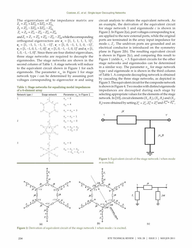
The eigenvalues of the impedance matrix areZ Z Z Z Za
a a a a= + + +11 12 13 142 2 ,Z Z Z Z Zb
a a a a= − + −11 12 13 142 2 ,Z Z Z Z Z Zc d
a a a a= = − − +11 12 13 14 and Z Z Z Z Z Ze f
a a a a= = + − −11 12 13 14, while the corresponding orthogonal eigenvectors are ea = [1, 1, 1, 1, 1, 1]T, eb = [1, −1, 1, −1, 1, −1]T, ec = [1, 0, −1, 1, 1, 0, −1]T, ed = [1, −1, 0, 1, −1, 0]T, ee = [1, 0, −1, −1, 0, 1]T and ef = [1, 1, 0, −1, −1, 0]T. Since there are four distinct eigenvalues, three stage networks are required to decouple the eigenmodes. The stage networks are shown in the second column of Table 1. A stage network will reduce to the equivalent circuit shown in Figure 1 for each eigenmode. The parameter nim in Figure 1 for stage network type i can be determined by assuming port voltages corresponding to eigenvector m and using
circuit analysis to obtain the equivalent network. As an example, the derivation of the equivalent circuit for stage network 1 and eigenmode c is shown in Figure 2. In Figure 2(a), port voltages corresponding to ec are applied to the new external ports, while the original ports are terminated in the array input impedance for mode c, Zc. The undriven ports are grounded and an electrical conductor is introduced on the symmetry plane in Figure 2(b). The resulting equivalent circuit is shown in Figure 2(c), and comparing this result to Figure 1 yields n1c = 3. Equivalent circuits for the other stage networks and eigenmodes can be determined in a similar way. The parameter nim for stage network type i and eigenmode m is shown in the third column of Table 1. A composite decoupling network is obtained by cascading the three stage networks, as depicted in Figure 3. The equivalent circuit for the composite network is shown in Figure 4. Two modes with distinct eigenmode impedances are decoupled during each stage by selecting appropriate values for the elements of the stage network. In [10], circuit elements (X1, B1), (X2, B2) and (X3,
B3) were obtained by setting ′ = ′Z Zc e , ′′ = ′′Z Zb c and ′′′= ′′′Z Za b ,
Table 1: Stage networks for equalizing modal impedances of a 6-element arrayNetwork type i Stage network Parameter nim in Figure 11 1
2
3
4'
5
6
5'
4
3'
6' 2'
1'jX
jB
n1a = 0
n1b = 4
n1c = n1d = 3
n1e = n1f = 1
2
4'
5' 3'
6' 2'
1'
jB
3
2
1
6
5
4
jX n2a = n2b = 0
n2c = n2d = n2e
= n2f = 3
3 1
2
3
4'
5
6
5'
4
3'
6' 2'
1'jX
jB
n3a = 0
n3b = n3c = n3d = n3e = n3f = 1
jX1'1
jnimB
Figure 1: Equivalent circuit of the stage network i when mode m is excited.
Figure 2: Derivation of equivalent circuit of the stage network 1 when mode c is excited.
Coetzee JC, et al.: Single-layer Decoupling Networks
235IETE TECHNICAL REVIEW | VOL 28 | ISSUE 3 | MAY-JUN 2011
and using closed-form expressions to determine the component values. Note that an implementation of the composite decoupling network shown in Figure 3 would require a multilayer circuit board or air bridge crossover structures.
In the alternative approach, we replace the Type 2 network with another Type 1 network in the composite decoupling network. The resulting composite network and its equivalent circuit are shown in Figures 5 and 6, respectively. From Figure 6, the input impedance observed at Ports 1' and 1" for mode m are given by
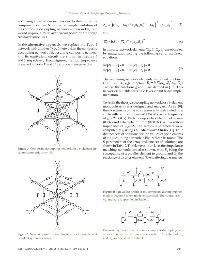
Figure 3: Composite decoupling network for a 6-element cir-culant symmetric array [10].
Figure 4: Equivalent circuit of the composite decoupling net-work in Figure 3 when mode m is excited. The values of n1m, n2m and n3m are specified in Table 1.
Figure 5: New composite decoupling network for a 6-element circulant symmetric array.
Coetzee JC, et al.: Single-layer Decoupling Networks
Figure 6: Equivalent circuit of new composite decoupling net-work in Figure 5 when mode m is excited. The values of n1m and n3m are specified in Table 1.
′ = + +( ) +( ) +
− − − −
Z Z jX jn B jX jn Bm m m m( )11
1 11
2
1
1 2
1
(7)
and
′′ = ′ + +( )− −Z Z jX jn Bm m m( )3
13 3
1. (8)
In this case, network elements (X1, B1, X2, B2) are obtained by numerically solving the following set of nonlinear equations:
Re[ ] , Im[ ]Re[ ] , Im[ ]
′ − ′ = ′ − ′ =′ − ′ = ′ − ′ =
Z Z Z ZZ Z Z Z
b c b c
b e b e
0 00 0 . (9)
The remaining network elements are found in closed f o r m a s X g Z Za b3 = ′′ ′′( , )a n dB h Z n Z n Xa a b b3 3 3 3= ′′ ′′( , , , , ), where the functions g and h are defined in [10]. This network is suitable for single-layer circuit board imple-mentation.
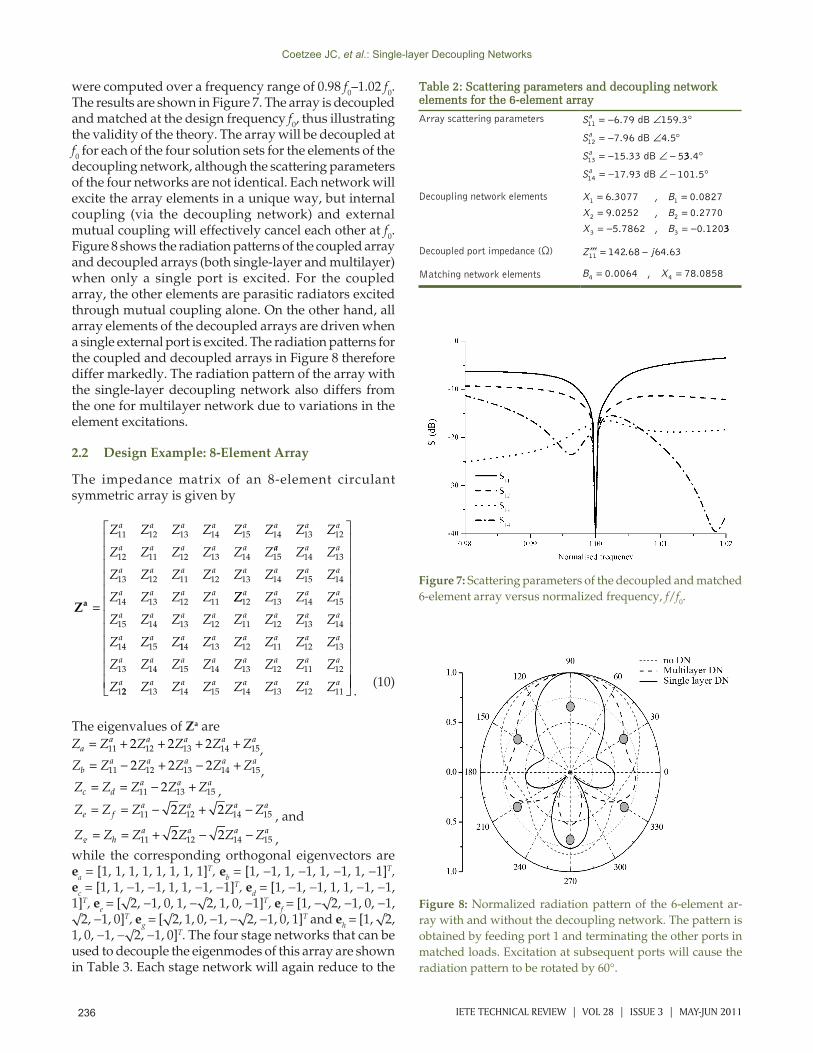
To verify the theory, a decoupling network for a 6-element monopole array was designed and analyzed. As in [10], the six elements of the array are evenly distributed on a circle with radius of 15 mm (0.125λ at a center frequency of f0 2 5= . GHz). Each monopole has a length of 28 mm (0.23λ) and a diameter of 1 mm (0.0083λ). With a system impedance of Z0=50Ω, the array’s S-parameters were computed at f0 using CST Microwave Studio [11]. Four distinct sets of solutions for the values of the elements of the decoupling network in Figure 5 can be found. The S-parameters of the array and one set of solutions are shown in Table 2. The elements of an L-section impedance matching networks are also shown, with B4 being the susceptance of a parallel element to ground and X4 the reactance of a series element. The scattering parameters
236 IETE TECHNICAL REVIEW | VOL 28 | ISSUE 3 | MAY-JUN 2011
were computed over a frequency range of 0.98 f0–1.02 f0. The results are shown in Figure 7. The array is decoupled and matched at the design frequency f0, thus illustrating the validity of the theory. The array will be decoupled at f0 for each of the four solution sets for the elements of the decoupling network, although the scattering parameters of the four networks are not identical. Each network will excite the array elements in a unique way, but internal coupling (via the decoupling network) and external mutual coupling will effectively cancel each other at f0. Figure 8 shows the radiation patterns of the coupled array and decoupled arrays (both single-layer and multilayer) when only a single port is excited. For the coupled array, the other elements are parasitic radiators excited through mutual coupling alone. On the other hand, all array elements of the decoupled arrays are driven when a single external port is excited. The radiation patterns for the coupled and decoupled arrays in Figure 8 therefore differ markedly. The radiation pattern of the array with the single-layer decoupling network also differs from the one for multilayer network due to variations in the element excitations.
2.2 Design Example: 8-Element Array
The impedance matrix of an 8-element circulant symmetric array is given by
Za =
Z Z Z Z Z Z Z Z
Z Z Z Z Z Z
a a a a a a a a
a a a a a11 12 13 14 15 14 13 12
12 11 12 13 14 15aa a a
a a a a a a a a
a a a a
Z Z
Z Z Z Z Z Z Z Z
Z Z Z Z
14 13
13 12 11 12 13 14 15 14
14 13 12 11 ZZ Z Z Z
Z Z Z Z Z Z Z Z
Z Z Z
a a a a
a a a a a a a a
a a
12 13 14 15
15 14 13 12 11 12 13 14
14 15 114 13 12 11 12 13
13 14 15 14 13 12 11 12
1
a a a a a a
a a a a a a a a
Z Z Z Z Z
Z Z Z Z Z Z Z Z
Z 22 13 14 15 14 13 12 11a a a a a a a aZ Z Z Z Z Z Z
. (10)
The eigenvalues of Za are Z Z Z Z Z Za
a a a a a= + + + +11 12 13 14 152 2 2 , Z Z Z Z Z Zb
a a a a a= − + − +11 12 13 14 152 2 2 ,Z Z Z Z Zc d
a a a= = − +11 13 152 ,Z Z Z Z Z Ze f
a a a a= = − + −11 12 14 152 2 , andZ Z Z Z Z Zg h
a a a a= = + − −11 12 14 152 2 , while the corresponding orthogonal eigenvectors are ea = [1, 1, 1, 1, 1, 1, 1, 1]T, eb = [1, −1, 1, −1, 1, −1, 1, −1]T, ec = [1, 1, −1, −1, 1, 1, −1, −1]T, ed = [1, −1, −1, 1, 1, −1, −1, 1]T, ee = [√2, −1, 0, 1, −√2, 1, 0, −1]T, ef = [1, −√2, −1, 0, −1, √2, −1, 0]T, eg = [√2, 1, 0, −1, −√2, −1, 0, 1]T and eh = [1, √2, 1, 0, −1, −√2, −1, 0]T. The four stage networks that can be used to decouple the eigenmodes of this array are shown in Table 3. Each stage network will again reduce to the
Figure 7: Scattering parameters of the decoupled and matched 6-element array versus normalized frequency, f/f0.
Figure 8: Normalized radiation pattern of the 6-element ar-ray with and without the decoupling network. The pattern is obtained by feeding port 1 and terminating the other ports in matched loads. Excitation at subsequent ports will cause the radiation pattern to be rotated by 60°.
Coetzee JC, et al.: Single-layer Decoupling Networks
Table 2: Scattering parameters and decoupling network elements for the 6-element arrayArray scattering parameters S
S
S
a
a
a
11
12
13
6 79 159 3
5
= − ∠ °
= − ∠ °
= − ∠ −
. . dB
7.96 dB 4.5
15.33 dB 33 4
17 93 101 514
.
. .
°
= − ∠ − °Sa dB
Decoupling network elements X B
X B
X B
1 1
2 2
3 3
= == == − = −
6.3077 0.0827
9.0252 0.2770
5.7862 0.120
,
,
, 33
Decoupled port impedance (Ω) ′′′ = −Z j11 1 4 6342 68 6. .
Matching network elements B X4 4= =0.0064 78.0858,
237IETE TECHNICAL REVIEW | VOL 28 | ISSUE 3 | MAY-JUN 2011
Table 3: Stage networks for equalizing modal impedances of an 8-element arrayNetwork type i Stage network Parameter nim in Figure 11
jBjX
1
4'5'
3
6'
2
1'
7'
8'
8
2'
3'
4
5
6
7
n1a = 0
n1b = 4
n1c = n1d = 2
n1e = n1f = 2 + √2
n1g = n1h = 2−√2
2
jB
jX
1
4'5'
3
6'
21'
7'
8'
8
2'
3'
4
5
6
7
n2a = n2b = 0
n2c = n2d = 4
n2e = n2f = n2g = n2h = 2
3
4'5'6'
1'
7'
8'
jX
jB
1
3
28
4
5
6
7
2'
3'
1
n3a = n3b = n3c = n3d = 0
n3e = n3f = n3g = n3h = 1
4
4'5'6'
1'
7'
8'
jX
jB
1
3
28
4
5
6
7
2'
3'
n4a = 0
n4b = n4c = n4d = n4e = n4f = n4g = n4h = 1
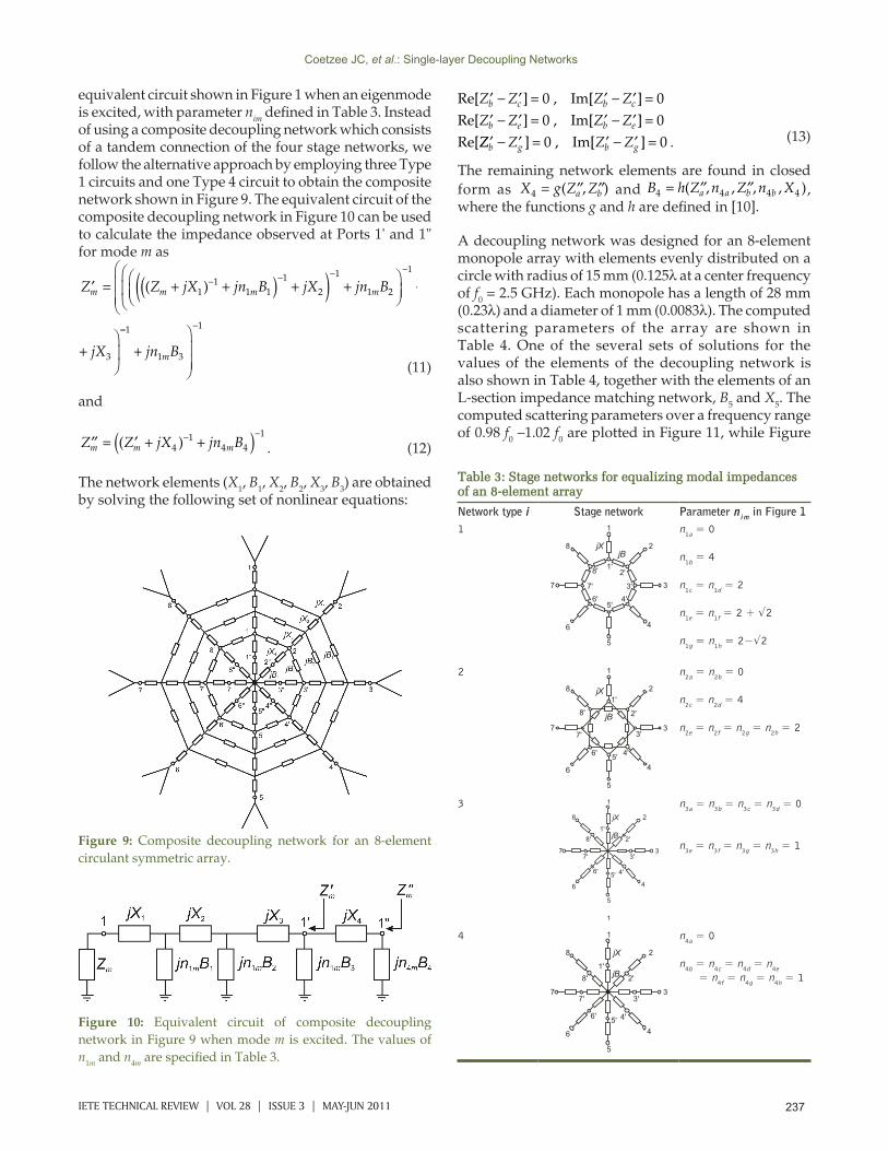
equivalent circuit shown in Figure 1 when an eigenmode is excited, with parameter nim defined in Table 3. Instead of using a composite decoupling network which consists of a tandem connection of the four stage networks, we follow the alternative approach by employing three Type 1 circuits and one Type 4 circuit to obtain the composite network shown in Figure 9. The equivalent circuit of the composite decoupling network in Figure 10 can be used to calculate the impedance observed at Ports 1' and 1" for mode m as
′ = + +( ) +( ) +
+
− − − −
Z Z jX jn B jX jn B jXm m m m( )11
1 11
2
1
1 2
1
3
−− −
+
1
1 3
1
jn Bm
′ = + +( ) +( ) +
+
− − − −
Z Z jX jn B jX jn B jXm m m m( )11
1 11
2
1
1 2
1
3
−− −
+
1
1 3
1
jn Bm (11)
and
′′ = ′ + +( )− −Z Z jX jn Bm m m( )4
14 4
1
. (12)
The network elements (X1, B1, X2, B2, X3, B3) are obtained by solving the following set of nonlinear equations:
Re[ ] , Im[ ]Re[ ] , Im[ ]Re[
′ − ′ = ′ − ′ =′ − ′ = ′ − ′ =′
Z Z Z ZZ Z Z Z
b c b c
b e b e
0 00 0
ZZ Z Z Zb g b g− ′ = ′ − ′ =] , Im[ ]0 0 . (13)
The remaining network elements are found in closed form as X g Z Za b4 = ′′ ′′( , ) and B h Z n Z n Xa a b b4 4 4 4= ′′ ′′( , , , , ), where the functions g and h are defined in [10].
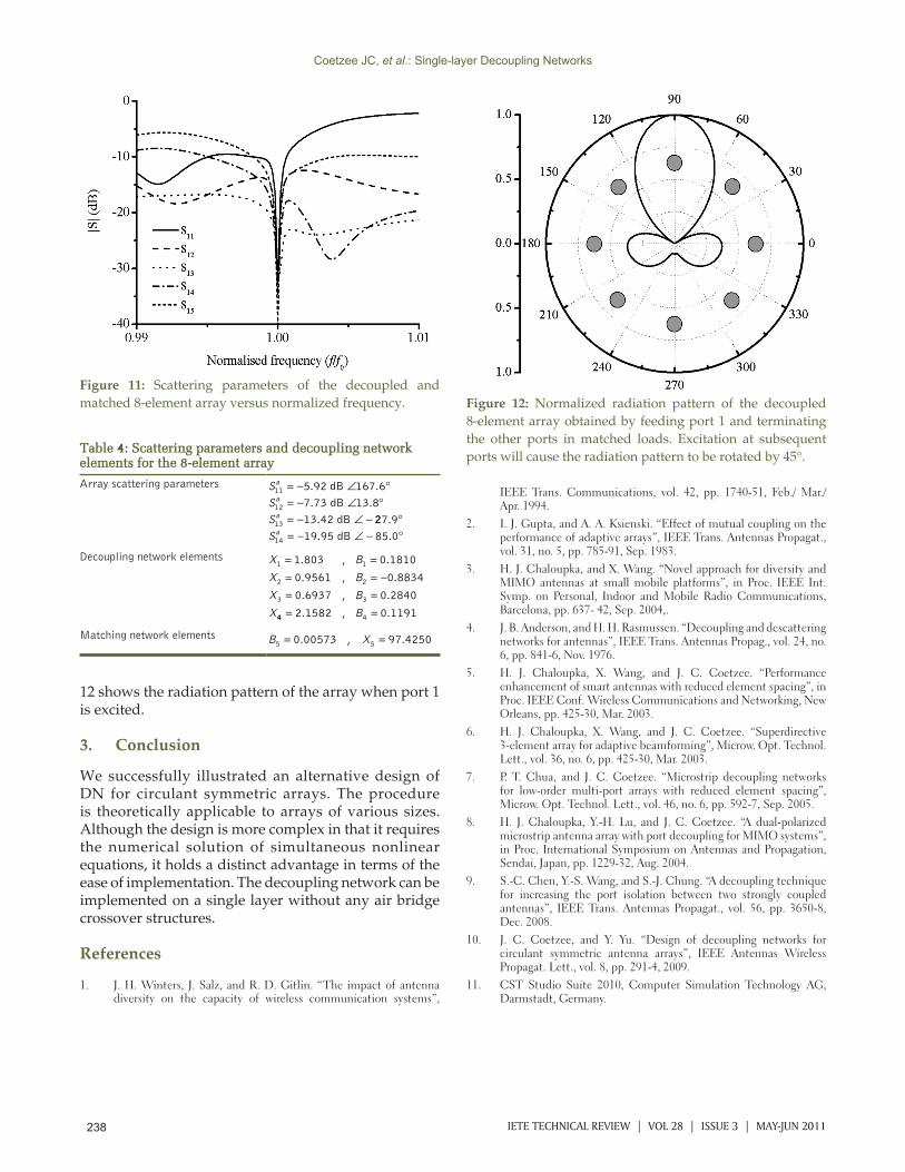
A decoupling network was designed for an 8-element monopole array with elements evenly distributed on a circle with radius of 15 mm (0.125λ at a center frequency of f0 = 2.5 GHz). Each monopole has a length of 28 mm (0.23λ) and a diameter of 1 mm (0.0083λ). The computed scattering parameters of the array are shown in Table 4. One of the several sets of solutions for the values of the elements of the decoupling network is also shown in Table 4, together with the elements of an L-section impedance matching network, B5 and X5. The computed scattering parameters over a frequency range of 0.98 f0 –1.02 f0 are plotted in Figure 11, while Figure
Figure 9: Composite decoupling network for an 8-element circulant symmetric array.
Figure 10: Equivalent circuit of composite decoupling network in Figure 9 when mode m is excited. The values of n1m and n4m are specified in Table 3.
Coetzee JC, et al.: Single-layer Decoupling Networks
238 IETE TECHNICAL REVIEW | VOL 28 | ISSUE 3 | MAY-JUN 2011
12 shows the radiation pattern of the array when port 1 is excited.
3. Conclusion
We successfully illustrated an alternative design of DN for circulant symmetric arrays. The procedure is theoretically applicable to arrays of various sizes. Although the design is more complex in that it requires the numerical solution of simultaneous nonlinear equations, it holds a distinct advantage in terms of the ease of implementation. The decoupling network can be implemented on a single layer without any air bridge crossover structures.
References
1. J. H. Winters, J. Salz, and R. D. Gitlin. “The impact of antenna diversity on the capacity of wireless communication systems”,
Table 4: Scattering parameters and decoupling network elements for the 8-element arrayArray scattering parameters S
SS
a
a
a
11
12
13
5 92 167 6= − ∠ °= − ∠ °= − ∠ −
. . dB 7.73 dB 13.813.42 dB 227 919 95 85 014
.. .
°= − ∠ − °Sa dB
Decoupling network elements X B
X B
X B
X
1 1
2 2
3 3
= == = −= =
1.803 0.1810
0.9561 0.8834
0.6937 0.2840
,
,
,
44 4= =2.1582 0.1191, B
Matching network elements B X5 5= =0.00573 97.4250,
Figure 11: Scattering parameters of the decoupled and matched 8-element array versus normalized frequency. Figure 12: Normalized radiation pattern of the decoupled
8-element array obtained by feeding port 1 and terminating the other ports in matched loads. Excitation at subsequent ports will cause the radiation pattern to be rotated by 45°.
IEEE Trans. Communications, vol. 42, pp. 1740-51, Feb./ Mar./ Apr. 1994.
2. I. J. Gupta, and A. A. Ksienski. “Effect of mutual coupling on the performance of adaptive arrays”, IEEE Trans. Antennas Propagat., vol. 31, no. 5, pp. 785-91, Sep. 1983.
3. H. J. Chaloupka, and X. Wang. “Novel approach for diversity and MIMO antennas at small mobile platforms”, in Proc. IEEE Int. Symp. on Personal, Indoor and Mobile Radio Communications, Barcelona, pp. 637- 42, Sep. 2004,.
4. J. B. Anderson, and H. H. Rasmussen. “Decoupling and descattering networks for antennas”, IEEE Trans. Antennas Propag., vol. 24, no. 6, pp. 841-6, Nov. 1976.
5. H. J. Chaloupka, X. Wang, and J. C. Coetzee. “Performance enhancement of smart antennas with reduced element spacing”, in Proc. IEEE Conf. Wireless Communications and Networking, New Orleans, pp. 425-30, Mar. 2003.
6. H. J. Chaloupka, X. Wang, and J. C. Coetzee. “Superdirective 3-element array for adaptive beamforming”, Microw. Opt. Technol. Lett., vol. 36, no. 6, pp. 425-30, Mar. 2003.
7. P. T. Chua, and J. C. Coetzee. “Microstrip decoupling networks for low-order multi-port arrays with reduced element spacing”, Microw. Opt. Technol. Lett., vol. 46, no. 6, pp. 592-7, Sep. 2005.
8. H. J. Chaloupka, Y.-H. Lu, and J. C. Coetzee. “A dual-polarized microstrip antenna array with port decoupling for MIMO systems”, in Proc. International Symposium on Antennas and Propagation, Sendai, Japan, pp. 1229-32, Aug. 2004.
9. S.-C. Chen, Y.-S. Wang, and S.-J. Chung. “A decoupling technique for increasing the port isolation between two strongly coupled antennas”, IEEE Trans. Antennas Propagat., vol. 56, pp. 3650-8, Dec. 2008.
10. J. C. Coetzee, and Y. Yu. “Design of decoupling networks for circulant symmetric antenna arrays”, IEEE Antennas Wireless Propagat. Lett., vol. 8, pp. 291-4, 2009.
11. CST Studio Suite 2010, Computer Simulation Technology AG, Darmstadt, Germany.
Author queries???AQ1: Running title missing - Author - (14_AP) - 02.04.11AQ2: Decoupling network has been abbreviated as DN only in the figure caption. Can it be used throughout the article? - Author - (14_AP) - 02.04.11AQ 4: Pls do the order of articles according to JOW??? - Deleted by satgheeshan - 02.04.11
Coetzee JC, et al.: Single-layer Decoupling Networks
239IETE TECHNICAL REVIEW | VOL 28 | ISSUE 3 | MAY-JUN 2011
Coetzee JC, et al.: Single-layer Decoupling Networks
AUTHORSJacob Coetzee was born in South Africa in 1964. He received the B.E. and M.E. Degrees (both with distinction) in 1986 and 1989 and a Ph.D. in electronic engineering from the University of Pretoria in 1994. He was with the Department of Electrical and Electronic Engineering, University of Pretoria from 1994 to 1997 and the Department of Electrical and Computer
Engineering, National University of Singapore from 1998 to 2007. He joined the School of Engineering Systems, Queensland University of Technology, Australia in 2008, where he is a Senior Lecturer. His research interests include antenna design, antenna arrays and passive microwave components.
E-mail: [email protected]
James D. Cordwell was born in Queensland, Australia in 1987. He graduated from Queensland University of Technology in 2009, with a Bachelor of Mathematics and Electrical Engineering. He currently works as a software engineer for the company GBST which develop software for the financial services industry. His research interests include passive microwave
DOI: ????; Paper No. TR 254_10; Copyright © 2011 by the IETE
components and antennae array design.
Elizabeth Underwood was born in Queensland, Australia in 1986. She graduated from Queensland University of Technology in 2010 with a B. Mathematics (Distinction) and a B. Electrical & Computer Engineering (Hons). She is currently a full-time mother of two children. Her research interests includes antenna array design and MIMO wireless channel
modelling.
Shauna Waite was born in Brisbane in 1988. She recieved a Bachelor of Mathematics (with Distinction) and Electrical Engineering (Hons) both in 2009. She is currently working as an electrical engineer in the building services and infrastructure industry. Her research interests include antenna arrays, control
systems and passive microwave components.