Embed Size (px)
Citation preview
© 2003 Cisco Systems, Inc. All right reserved. Important notices, privacy statements, and trademarks of Cisco Systems, Inc. can be found on cisco.com
Page 1 of 30
Optical Technologies for Next-Generation Metro DWDM Applications 1 Abstract
Over the course of the past few years the characteristics of Metropolitan DWDM networks have evolved considerably. Just few years ago a typical Metro DWDM system had 16x2.5 Gbit/s channels, 200 GHz spacing and un-amplified spans. Nowadays the average system supports 32x10 Gbit/s, 100 GHz spacing, optical amplification and chromatic dispersion compensation to cover distances of over 200 km. The next generation of Metro DWDM systems will raise the bar even further with respect to channel densities and distances, while continuing to reduce the footprint, the power consumption and increasing the flexibility of optical DWDM systems. The real engine behind the scenes of the rapid evolution of Metro DWDM networks is the relentless advancement in optical components and semiconductor technologies, which allows integrating on a single Photonic Integrated Circuit (PIC1) a variety of optical devices and functions. This technical paper describes some (yes just some) of the new developments, which will characterize Metro DWDM, as well as some consolidated technologies, once exclusively deployed in Long Haul networks, soon required in Metro applications.
1 A PIC or Photonic Integrated Circuit is a semiconductor technology to integrate various lightwave components on the same silicon chip. A PIC allows integrating components such as a laser, a modulator, a VOA and a power monitor, just to name a few, in a single package. Among the main benefits versus discrete components technologies are higher densities and reduced power consumptions.
CISCO TECHNOLOGY MARKETING

Cisco Confidential Copyright © 2002 Cisco Systems, Inc. All rights reserved.
Page 2 of 30
Contents
1 Abstract..................................................................................................................................................................................... 1
2 Fixed Wavelength and Tunable Lasers Technologies Overview ................................................................................... 4
2.1 Fixed Wavelength Lasers for DWDM applications................................................................................................. 4
2.2 Tunable DFB Laser........................................................................................................................................................ 5
2.2.1 Tunable Distributed Bragg Reflector (DBR) Laser ........................................................................................ 5
2.2.2 Grating-Assisted Co-directional Coupler (GACC) Laser.............................................................................. 5
2.2.3 Sampled Grating DBR (SG-DBR) ..................................................................................................................... 6
2.2.4 External Cavity Tunable Laser (ECL)............................................................................................................... 7
2.2.5 Tunable Laser Technology summary chart ...................................................................................................... 8
3 A Word on Direct Modulation.............................................................................................................................................. 8
4 External Modulators............................................................................................................................................................... 9
4.1 Electro-absorption Modulator.................................................................................................................................... 10
4.2 Electro-optic Modulators ............................................................................................................................................ 10
4.2.1 Lithium Niobate (LiNbO3) Modulators........................................................................................................... 11
4.2.2 Semiconductor Electro-optic (Interferometric) Modulators ........................................................................ 11
4.3 Comparison Electro -absorption vs. Electro-optic modulators ............................................................................. 11
4.4 Metro Optical Interfaces Transmitter Technologies .............................................................................................. 12
5 Photodetectors ....................................................................................................................................................................... 12
6 Modulation Formats ............................................................................................................................................................. 14
6.1 Why new modulation formats beyond NRZ or RZ? .............................................................................................. 15
6.1.1 Spectral Efficiency.............................................................................................................................................. 15
6.1.2 Improving Optical Signal Performance........................................................................................................... 16
6.2 Duobinary Modulation................................................................................................................................................ 17
6.2.1 Logical Duobinary Signal Generation............................................................................................................. 17
6.2.2 Duobinary Signaling in the optical domain .................................................................................................... 20
6.2.3 Duobinary signaling practical implementations............................................................................................ 22
7 Wavelength locker................................................................................................................................................................ 23

Cisco Confidential Copyright © 2002 Cisco Systems, Inc. All rights reserved.
Page 3 of 30
7.1 Wavelength Locker: Principle and Operations....................................................................................................... 24
8 Introduction to Forward Error Correction (FEC)............................................................................................................ 26
8.1 FEC performance ......................................................................................................................................................... 26
8.2 FEC codes for Optical Communications.................................................................................................................. 27
9 Electronic Equalization........................................................................................................................................................ 28
9.1 Basic Equalization Principle ...................................................................................................................................... 29
10 Abbreviations.................................................................................................................................................................... 30
© 2003 Cisco Systems, Inc. All right reserved. Important notices, privacy statements, and trademarks of Cisco Systems, Inc. can be found on cisco.com
Page 4 of 30
2 Fixed Wavelength and Tunable Lasers Technologies Overview
Telecommunication lasers have evolved substantially since the introduction of the early AlGaAs-based semiconductor lasers in the late 1970s suitable for transmitting multimode light at 850 nm. Focusing on DWDM applications (in the 1550 nm window) Distributed Feedback (DFB) lasers are today’s incumbent. However with the advent of Tunable Laser Technologies, whose most immediate benefit is the ability to reduce inventory levels, a new breed of lasers based on some variant of the Distributed Bragg Reflector (DBR), or External Cavity Laser (ECL) structure represents a more viable alternative to DFB lasers. The next few paragraphs are an overview of the fixed wavelengths and tunable laser technologies.
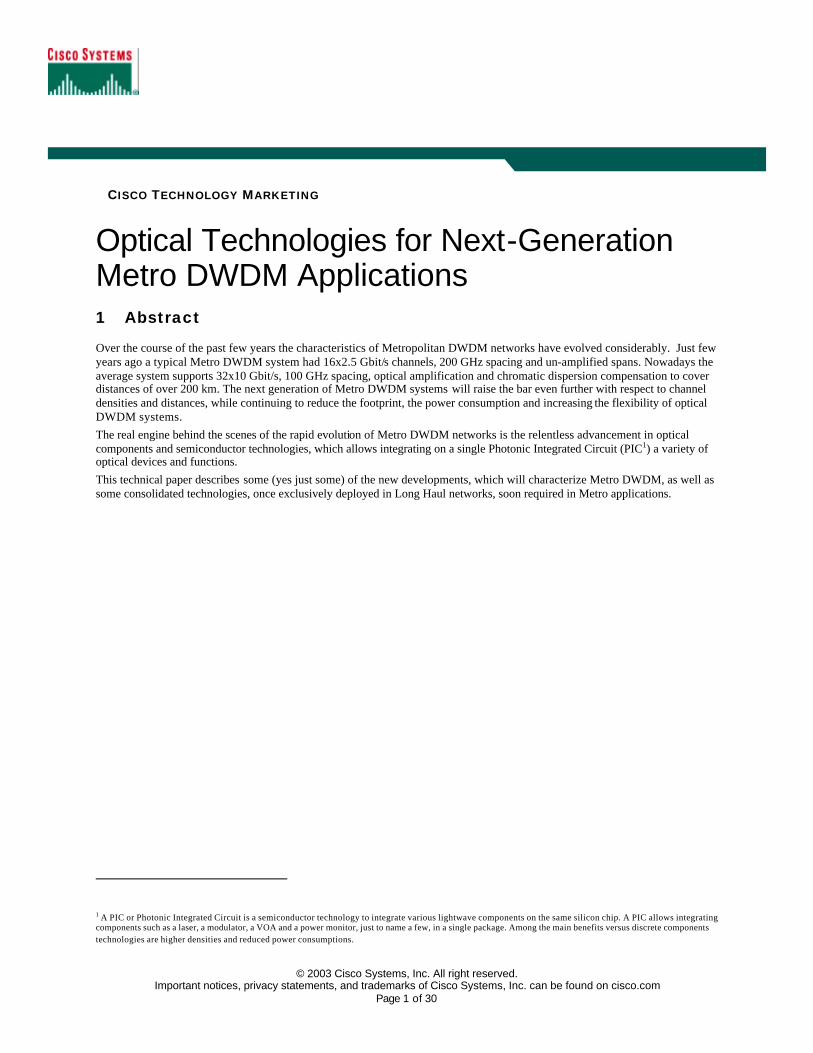
Figure 1: Schematic side view of DFB laser
2.1 Fixed Wavelength Lasers for DWDM applications
DFB lasers are the technology of choice for fixed wavelength DWDM transmitters. (As explained later, DFB lasers can also act as temperature-controlled tunable lasers, but with significant limitations). In a DFB laser, a grating (dotted line) is formed by etching a periodic corrugation into the waveguide active layer (solid line). The grating acts as a series of distributed tiny mirrors (feedback devices), on which the light bounces back and forth allowing only one mode to survive in the cavity (see Figure 1). The operating wavelength of the laser is controlled by the period of the grating. DFB lasers have usually a very narrow spectral line of few MHz (without modulation) and exhibit Side Mode Suppression Ratios (SMSR) in excess of 40dB (see Figure 2).
Figure 2: DFB laser spectrum (1.25 Gbit/s direct modulation)
Laser Dominant Mode
Suppressed Modes
SMSR
contact
grating
ground
Highly Reflecting Mirror Anti Reflecting
Mirror
light Active waveguide
Cisco Confidential Copyright © 2002 Cisco Systems, Inc. All rights reserved.
Page 5 of 30
2.2 Tunable DFB Laser
Perhaps the simplest type of tunable laser is a thermally tuned DFB. The intra-cavity grating, which determines the wavelength, is a periodic corrugation of the refractive index. The refractive index exhibits temperature dependence, therefore by thermal tuning it is possible to modify the grating period and select the laser wavelength.
For a typical DFB the thermal tuning coefficient is in the order of 0.1 nm/°C, this means that for 3 nm tuning range, a 30 °C temperature excursion is required. These figures can give the feeling why practical devices can be tuned over just few nanometers (practical devices can be tuned maximum over 5 nm).
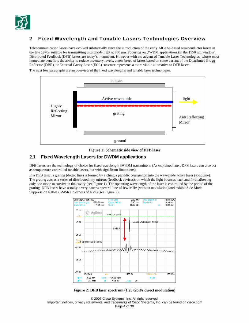
2.2.1 Tunable Distributed Bragg Reflector (DBR) Laser
One of the earliest types of tunable lasers is the distributed Bragg reflector laser. More modern tunable devices still share the same basic concepts and can be considered an evolution of DBR lasers. Like in DFB laser a DBR introduces a periodic variation of the refractive index effectively generating a Bragg grating or reflector (dotted line). The cleaved front facet of the device acts as a second mirror. (The “phase” section is adjusted to assure that the roundtrip phase condition is matched). Only the wavelengths in a specific relation with the Bragg period survive in the cavity. Tuning is achieved by injecting current into the Bragg reflector. This results in a modification of the refractive index, which causes the Bragg peak to tune to different wavelengths. The Phase Section is primarily designed for fine-tuning the output wavelength.
Figure 3: Schematic side view of 3-section DBR laser
The tuning range of these devices is proportional to the maximum change in the refractive index, typically below 20 nm. To overcome this limitation new types of devices have been developed. The following two paragraphs analyze a couple of this DBR variant just as an example. Many more tuning schemes exist, to improve tuning range, tuning speed and spectral line purity.
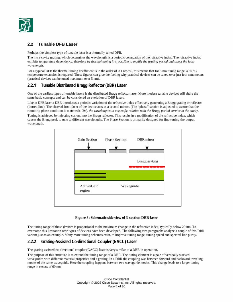
2.2.2 Grating-Assisted Co-directional Coupler (GACC) Laser
The grating assisted co-directional coupler (GACC) laser is very similar to a DBR in operation. The purpose of this structure is to extend the tuning range of a DBR. The tuning element is a pair of vertically stacked waveguides with different material properties and a grating. In a DBR the coupling was between forward and backward traveling modes of the same waveguide. Here the coupling happens between two waveguide modes. This change leads to a larger tuning range in excess of 60 nm.
Bragg grating
Waveguide
Gain Section
Active/Gain region
Phase Section DBR mirror
Cisco Confidential Copyright © 2002 Cisco Systems, Inc. All rights reserved.
Page 6 of 30
Figure 4: Schematic side view of GACC laser
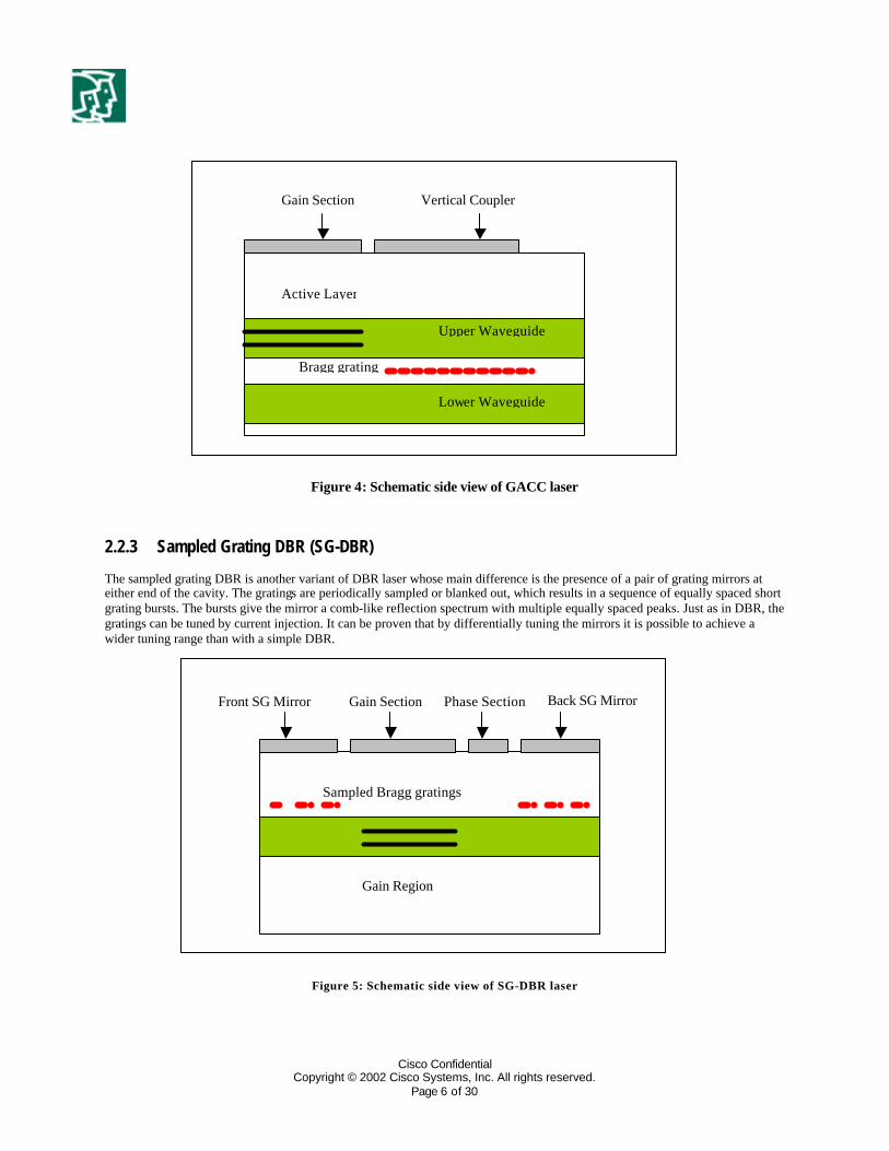
2.2.3 Sampled Grating DBR (SG-DBR)
The sampled grating DBR is another variant of DBR laser whose main difference is the presence of a pair of grating mirrors at either end of the cavity. The gratings are periodically sampled or blanked out, which results in a sequence of equally spaced short grating bursts. The bursts give the mirror a comb-like reflection spectrum with multiple equally spaced peaks. Just as in DBR, the gratings can be tuned by current injection. It can be proven that by differentially tuning the mirrors it is possible to achieve a wider tuning range than with a simple DBR.
Figure 5: Schematic side view of SG-DBR laser
Bragg grating
Lower Waveguide
Gain Section
Active Layer
Vertical Coupler
Upper Waveguide
Sampled Bragg gratings
Front SG Mirror
Gain Region
Back SG Mirror Gain Section Phase Section
Cisco Confidential Copyright © 2002 Cisco Systems, Inc. All rights reserved.
Page 7 of 30
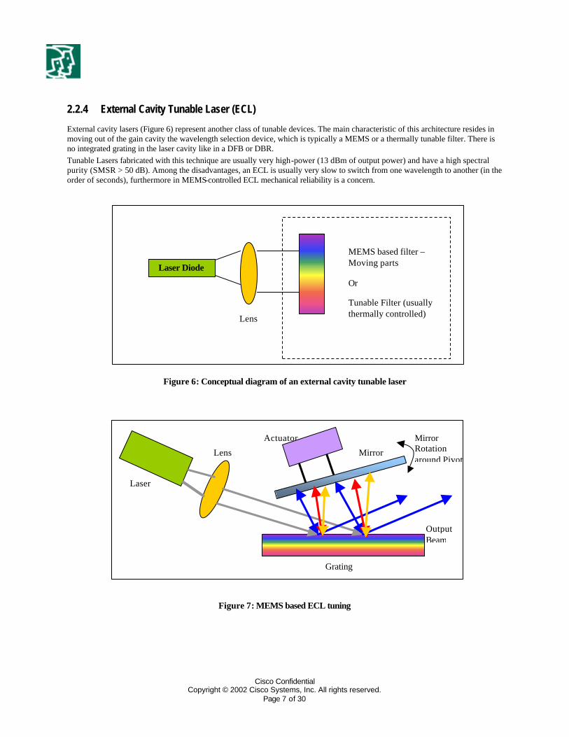
2.2.4 External Cavity Tunable Laser (ECL)
External cavity lasers (Figure 6) represent another class of tunable devices. The main characteristic of this architecture resides in moving out of the gain cavity the wavelength selection device, which is typically a MEMS or a thermally tunable filter. There is no integrated grating in the laser cavity like in a DFB or DBR. Tunable Lasers fabricated with this technique are usually very high-power (13 dBm of output power) and have a high spectral purity (SMSR > 50 dB). Among the disadvantages, an ECL is usually very slow to switch from one wavelength to another (in the order of seconds), furthermore in MEMS-controlled ECL mechanical reliability is a concern.
Figure 6: Conceptual diagram of an external cavity tunable laser
Figure 7: MEMS based ECL tuning
FP DiodLae
Lens
MEMS based filter – Moving parts
Or
Tunable Filter (usually thermally controlled)
Laser Diode
Lens
Laser
Mirror
Output Beam
Actuator Mirror Rotation around Pivot
Grating
Cisco Confidential Copyright © 2002 Cisco Systems, Inc. All rights reserved.
Page 8 of 30
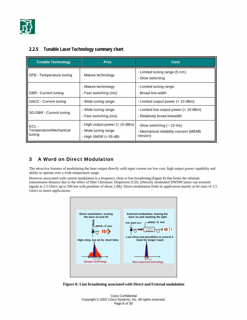
2.2.5 Tunable Laser Technology summary chart
Tunable Technology Pros Cons
DFB - Temperature tuning - Mature technology - Limited tuning range (5 nm)
- Slow switching
DBR - Current tuning
- Mature technology
- Fast switching (ms)
- Limited tuning range
- Broad line width
GACC - Current tuning - Wide tuning range - Limited output power (< 10 dBm)
SG-DBR - Current tuning - Wide tuning range
- Fast switching (ms)
- Limited low output power (< 10 dBm)
- Relatively broad linewidth
ECL - Temperature/Mechanical tuning
- High output power (> 10 dBm)
- Wide tuning range
- High SMSR (> 55 dB)
- Slow switching (~ 10 ms)
- Mechanical reliability concern (MEMS version)
3 A Word on Direct Modulation
The attractive features of modulating the laser output directly with input current are low cost, high output power capability and ability to operate over a wide temperature range. However associated with current modulation is a frequency chirp or line broadening (Figure 8) that limits the ultimate transmission distance due to the effect of fiber Chromatic Dispersion (CD). (Directly modulated DWDM lasers can transmit signals at 2.5 Gbit/s up to 200 km with penalties of about 2 dB). Direct modulation finds its application mainly at bit rates of 2.5 Gbit/s in metro applications.
External modulation: leaving the laser on and masking the light
Direct modulation: turning the laser on and off
More expensive technology
Low chirp and possibility to control itUsed for longer reachHigh chirp, but ok for short links
Cheaper technology
DFB, MQW laser
–~0.5 nm –0.02 nm
MODExternal
Modulator
MOD
Figure 8: Line broadening associated with Direct and External modulation
Cisco Confidential Copyright © 2002 Cisco Systems, Inc. All rights reserved.
Page 9 of 30
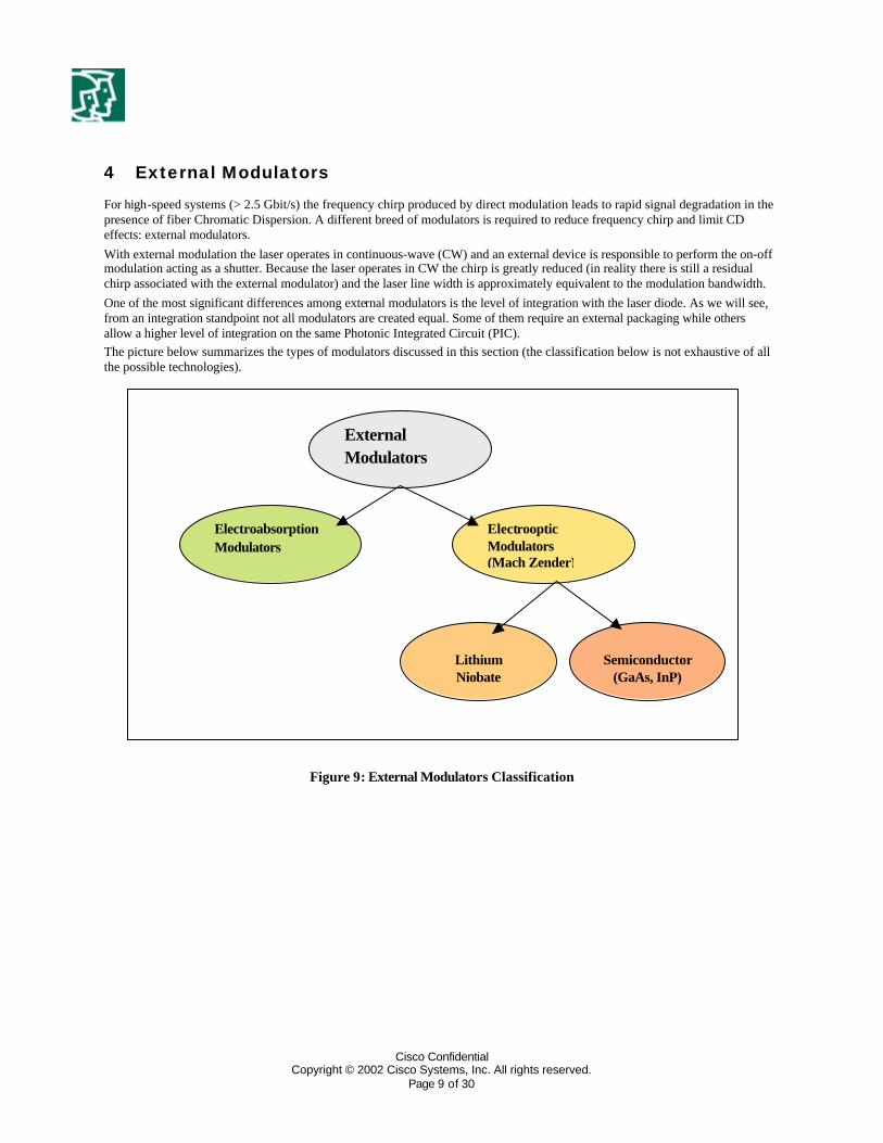
4 External Modulators For high-speed systems (> 2.5 Gbit/s) the frequency chirp produced by direct modulation leads to rapid signal degradation in the presence of fiber Chromatic Dispersion. A different breed of modulators is required to reduce frequency chirp and limit CD effects: external modulators. With external modulation the laser operates in continuous-wave (CW) and an external device is responsible to perform the on-off modulation acting as a shutter. Because the laser operates in CW the chirp is greatly reduced (in reality there is still a residual chirp associated with the external modulator) and the laser line width is approximately equivalent to the modulation bandwidth. One of the most significant differences among external modulators is the level of integration with the laser diode. As we will see, from an integration standpoint not all modulators are created equal. Some of them require an external packaging while others allow a higher level of integration on the same Photonic Integrated Circuit (PIC). The picture below summarizes the types of modulators discussed in this section (the classification below is not exhaustive of all the possible technologies).
Figure 9: External Modulators Classification
External Modulators
Electrooptic Modulators (Mach Zender)
Electroabsorption Modulators
Lithium Niobate
Semiconductor (GaAs, InP)
© 2003 Cisco Systems, Inc. All right reserved. Important notices, privacy statements, and trademarks of Cisco Systems, Inc. can be found on cisco.com
Page 10 of 30
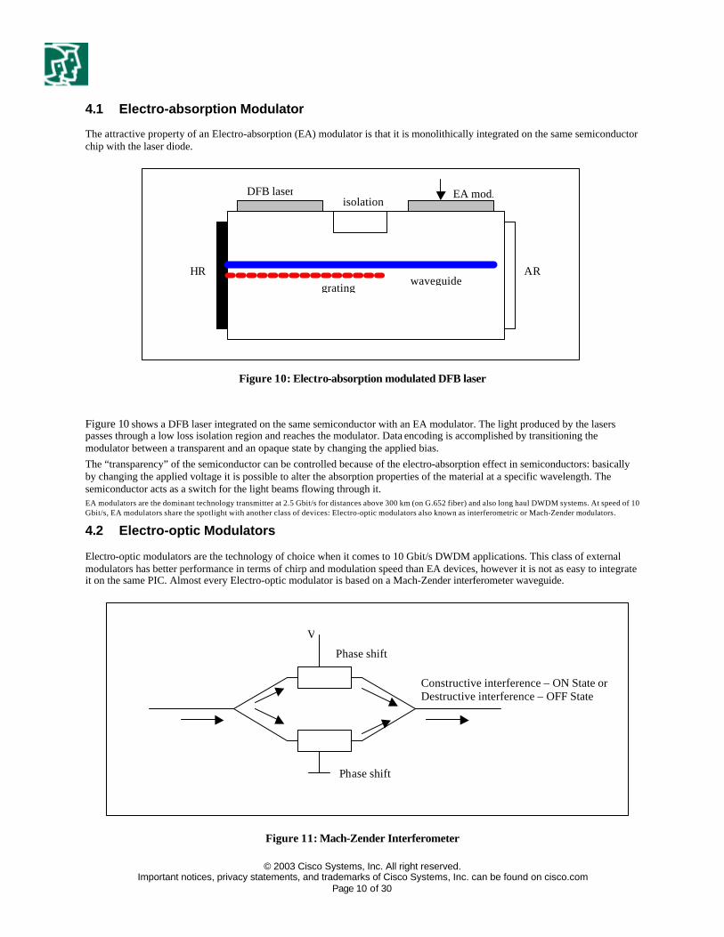
4.1 Electro-absorption Modulator
The attractive property of an Electro-absorption (EA) modulator is that it is monolithically integrated on the same semiconductor chip with the laser diode.
Figure 10: Electro-absorption modulated DFB laser
Figure 10 shows a DFB laser integrated on the same semiconductor with an EA modulator. The light produced by the lasers passes through a low loss isolation region and reaches the modulator. Data encoding is accomplished by transitioning the modulator between a transparent and an opaque state by changing the applied bias. The “transparency” of the semiconductor can be controlled because of the electro-absorption effect in semiconductors: basically by changing the applied voltage it is possible to alter the absorption properties of the material at a specific wavelength. The semiconductor acts as a switch for the light beams flowing through it. EA modulators are the dominant technology transmitter at 2.5 Gbit/s for distances above 300 km (on G.652 fiber) and also long haul DWDM systems. At speed of 10 Gbit/s, EA modulators share the spotlight with another class of devices: Electro-optic modulators also known as interferometric or Mach-Zender modulators.
4.2 Electro-optic Modulators
Electro-optic modulators are the technology of choice when it comes to 10 Gbit/s DWDM applications. This class of external modulators has better performance in terms of chirp and modulation speed than EA devices, however it is not as easy to integrate it on the same PIC. Almost every Electro-optic modulator is based on a Mach-Zender interferometer waveguide.
Figure 11: Mach-Zender Interferometer
isolation DFB laser EA mod.
waveguide HR AR
grating
V
Phase shift
Phase shift
Constructive interference – ON State or Destructive interference – OFF State
Cisco Confidential Copyright © 2002 Cisco Systems, Inc. All rights reserved.
Page 11 of 30
In a Mach-Zender modulator, the incoming light is split in a Y branch. When the light from the upper and lower waveguides recombines in the output Y branch, there is either a constructive or a destructive interference depending on the optical path difference between the two branches. It is possible to alter this path difference by applying an electric field to the two waveguides. The voltage changes the refractive index by electro-optic effect. For example the modulator is switched in “off” when the applied voltage causes a mismatch in the speed of light in the two waveguides such that the two optical beams at the output Y branch are in opposite phase; this condition is referred as destructive interference, because the two beams cancel each other out when recombining. Although every Mach-Zender modulator shares the same operating principles there are various types of modulators that can be classified based on the material used in the substrate.
4.2.1 Lithium Niobate (LiNbO3) Modulators
Lithium Niobate is the most popular material to build of Electro-optic modulators due to its excellent electro-optic properties, very high-speed modulation capabilities, low chirp and high extinction ratio. However since LiNbO3 is not a semiconductor substrate, these devices require external packaging. Another drawback is typically a higher driving voltage than EA components.
4.2.2 Semiconductor Electro-optic (Interferometric) Modulators
Recently new technological advances made possible to explore semiconductor materials as a substrate for Mach-Zender devices. By using GaAs or InP substrates it is possible to achieve high level of integration on the same PIC (similar to EA modulators). For example the new generation of PIC can integrate laser, Interferometric Modulator, SOA, VOA and power tap monitors.
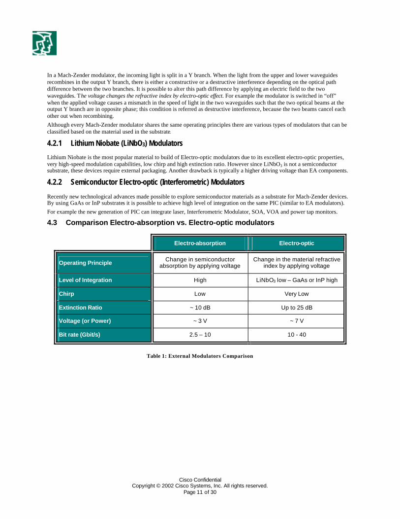
4.3 Comparison Electro-absorption vs. Electro-optic modulators
Electro-absorption Electro-optic
Operating Principle Change in semiconductor absorption by applying voltage
Change in the material refractive index by applying voltage
Level of Integration High LiNbO3 low – GaAs or InP high
Chirp Low Very Low
Extinction Ratio ~ 10 dB Up to 25 dB
Voltage (or Power) ~ 3 V ~ 7 V
Bit rate (Gbit/s) 2.5 – 10 10 - 40
Table 1: External Modulators Comparison
Cisco Confidential Copyright © 2002 Cisco Systems, Inc. All rights reserved.
Page 12 of 30
4.4 Metro Optical Interfaces Transmitter Technologies
Typical 10 Gbit/s ITU card
Typical 2.5 Gbit/s ITU card
(external modulation)
Typical 2.5 Gbit/s ITU card (direct modulation)
Modulator LiNb03 EA Direct Mod.
Extinction Ratio (dB) 10 10 9
Dispersion Tolerance2 (ps/nm) ± 1200 5400 1800/3200
Table 2: Metro DWDM Transmitters
Typical 10 Gbit/s ITU card
Typical 2.5 Gbit/s ITU card
Modulator LiNb03 LiNb03
Extinction Ratio (dB) 11 12
Dispersion Tolerance3 (ps/nm) ± 800 ± 12800
Table 3: Long Haul DWDM Transmitters
5 Photodetectors
With virtually no exception, commercial DWDM systems detect the power (or the square of the electric field) of the incoming optical signal. The basic function of a photodetector is to convert the optical power into electrical current. A simplified functional diagram of a photodetector is composed of a semiconductor diode followed by a trans-impedance amplifier4 (TIA), a clock recovery block and a demodulator circuit.
2 Dispersion Tolerance depends also on the receiver performance; nonetheless the table gives an idea of the different performance associated with the various technologies.
3 A 2dB OSNR Penalty is assumed.
4 A TIA acts as a current-to-voltage converter.
Cisco Confidential Copyright © 2002 Cisco Systems, Inc. All rights reserved.
Page 13 of 30
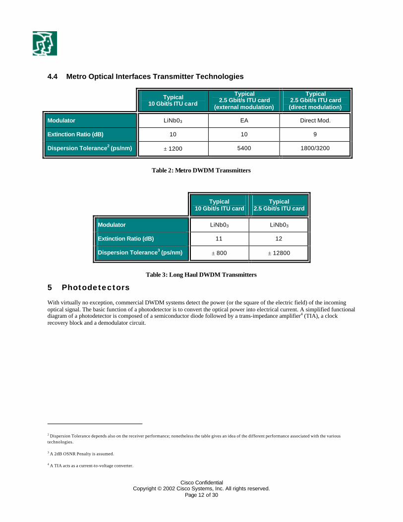
Figure 12: Input Optical Power and Output Photodiode current
There are two types of photodetectors: Avalanche Photo Diode5 (APD) and PIN6 photodetector. In both devices the light-to-current (O-E) conversion process is the same: the energy of an incident photon is absorbed by the semiconductor and converted into a pair of electron-hole carriers; the bias applied to the diode moves (in opposite direction) the electron and the hole producing current. The operational difference between a PIN and an APD resides in how strong is the applied bias: in an APD the very strong bias applied to the diode accelerates the electrons, giving them enough kinetic energy to allow them to create other electron-hole pairs when colliding with other particles (avalanche effect). In an APD from one photon, we have multiple hole-electron pairs. There is an intrinsic amplification effect. In a PIN, the bias is smaller and there is a one-to-one correspondence between photons and carriers. An APD typically has a better sensitivity making it suitable for metro DWDM transmission, which is often power limited. On the other hand a PIN has a better noise characteristic than an APD, where the avalanche effect is also a source of electrical noise. A PIN is usually the choice for long-haul systems where the system is OSNR-limited, while metro DWDM platforms typically employ APD receivers.
5 The APD is named after the physical principle behind the one-photon-to-many-carrier generation: the avalanche effect.
6 A PIN photodetector takes his name from the semiconductor layers used to build it. A p -doped layer, an n -doped layer and, sandwiched in between, an intrinsic (i) layer with just a light doping. The presence of an intrinsic layer has several advantages over a simple p -n diode, like increasing the area for capturing light and increasing the carrier transit time which eventually translates into higher supported bit-rates.
Optical Signal
TIA
Input Optical Power (Pin)
Output Current (Iout)
Slope = Responsivity (A/W)
Iout = R*Pin = R*E2
1. The output current is proportional to the input power and the coefficient is known as responsivity (R).
2. E2 is the square of the electric field of the optical signal: the photodiode is also known as square-law device
Iout
Cisco Confidential Copyright © 2002 Cisco Systems, Inc. All rights reserved.
Page 14 of 30
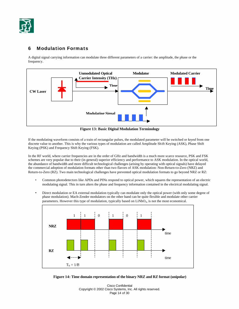
6 Modulation Formats
A digital signal carrying information can modulate three different parameters of a carrier: the amplitude, the phase or the frequency.
Figure 13: Basic Digital Modulation Terminology If the modulating waveform consists of a train of rectangular pulses, the modulated parameter will be switched or keyed from one discrete value to another. This is why the various types of modulation are called Amplitude Shift Keying (ASK), Phase Shift Keying (PSK) and Frequency Shift Keying (FSK).
In the RF world, where carrier frequencies are in the order of GHz and bandwidth is a much more scarce resource, PSK and FSK schemes are very popular due to their (in general) superior efficiency and performance to ASK modulation. In the optical world, the abundance of bandwidth and more difficult technological challenges (arising by operating with optical signals) have delayed the commercial adoption of modulation formats other than two flavors of ASK modulation: Non-Return-to-Zero (NRZ) and Return-to-Zero (RZ). Two main technological challenges have prevented optical modulation formats to go beyond NRZ or RZ:
• Common photodetectors like APDs and PINs respond to optical power, which squares the representation of an electric modulating signal. This in turn alters the phase and frequency information contained in the electrical modulating signal.
• Direct modulation or EA external modulation typically can modulate only the optical power (with only some degree of phase modulation). Mach-Zender modulators on the other hand can be quite flexible and modulate other carrier parameters. However this type of modulation, typically based on LiNbO3, is not the most economical.
Figure 14: Time domain representation of the binary NRZ and RZ format (unipolar)
Modulating Signal
Modulator
CW Laser
Unmodulated Optical Carrier Intensity (THz)
Time Time
Modulated Carrier
Time
time
time
1 1 1 1 0 0
NRZ
RZ
Tb = 1/B
Cisco Confidential Copyright © 2002 Cisco Systems, Inc. All rights reserved.
Page 15 of 30
This section covers the popular NRZ and RZ schemes and also presents a new format, duobinary modulation, which is a good candidate to be adopted in the next generation of 10 Gbit/s optical transponders.
6.1 Why new modulation formats beyond NRZ or RZ?
The reason behind the need to explore new modulation schemes is twofold: improving spectral efficiency and improving optical performance. The two reasons are discussed separately.
6.1.1 Spectral Efficiency
Spectral efficiency is defined as the ratio of the individual channel bit rate to the DWDM channel separation.
Bit Rate (Gbit/s)
Channel Spacing (GHz)
Spectral Efficiency
2.5 100/50 0.025/0.05
10 100/50 0.1/0.2
40 100/50 0.4/0.8
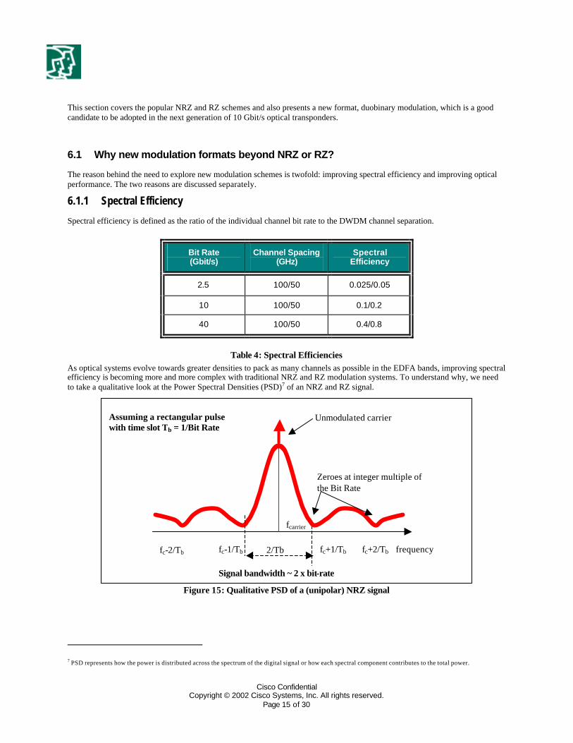
Table 4: Spectral Efficiencies As optical systems evolve towards greater densities to pack as many channels as possible in the EDFA bands, improving spectral efficiency is becoming more and more complex with traditional NRZ and RZ modulation systems. To understand why, we need to take a qualitative look at the Power Spectral Densities (PSD)7 of an NRZ and RZ signal.
Figure 15: Qualitative PSD of a (unipolar) NRZ signal
7 PSD represents how the power is distributed across the spectrum of the digital signal or how each spectral component contributes to the total power.
fcarrier
fc+1/Tb fc+2/Tb fc-1/Tb fc-2/Tb frequency
Assuming a rectangular pulse with time slot Tb = 1/Bit Rate
Signal bandwidth ~ 2 x bit-rate
Unmodulated carrier
Zeroes at integer multiple of the Bit Rate
2/Tb
Cisco Confidential Copyright © 2002 Cisco Systems, Inc. All rights reserved.
Page 16 of 30
In the frequency domain a NRZ binary sequence of bits occupies a bandwidth8 twice the modulation bit rate9. In other words a signal modulated at 10 Gbit/s has a bandwidth of about 20 GHz. Moreover part of the energy is still associated with the unmodulated carrier (i.e. it is not used to carry information.)
Figure 16: NRZ signal eye diagram The PSD of an RZ signal (see Figure 17) shows that this format occupies twice the bandwidth of an NRZ signal and tones appear at odd integer multiples of the bit rate. As an example a 10 Gbit/s signal occupies a bandwidth of about 40 GHz.
Figure 17: Qualitative PSD of a (unipolar) RZ signal
Having modulation schemes with reduced bandwidth allows reducing the channel spacing without incurring in channel overlap or cross-talk.
6.1.2 Improving Optical Signal Performance
Modulation formats also exhibits different behavior towards various transmission impairments. By choosing other modulation schemes it is possible to make the signal more robust towards chromatic dispersion, polarization mode dispersion, nonlinear effects and signal-to-noise ratio degradations.
8 A convenient way to define bandwidth is as spectral width between the two closest null points (or zeroes) to the carrier frequency.
9 With filtering techniques to shape the pulses it is actually possible to reduce the spectral width of NRZ and RZ signals, thus improving performance.
fc+2/Tb fc+4/Tb fc-2/Tb fc-4/Tb frequency
Signal bandwidth ~ 4 x bit-rate
4/Tb
fcarrier
Assuming a rectangular pulse with time slot Tb = 1/Bit Rate unmodulated carrier
Zeroes at integer multiple of twice the Bit Rate
Tones at odd integers multiple of the Bit Rate
Cisco Confidential Copyright © 2002 Cisco Systems, Inc. All rights reserved.
Page 17 of 30
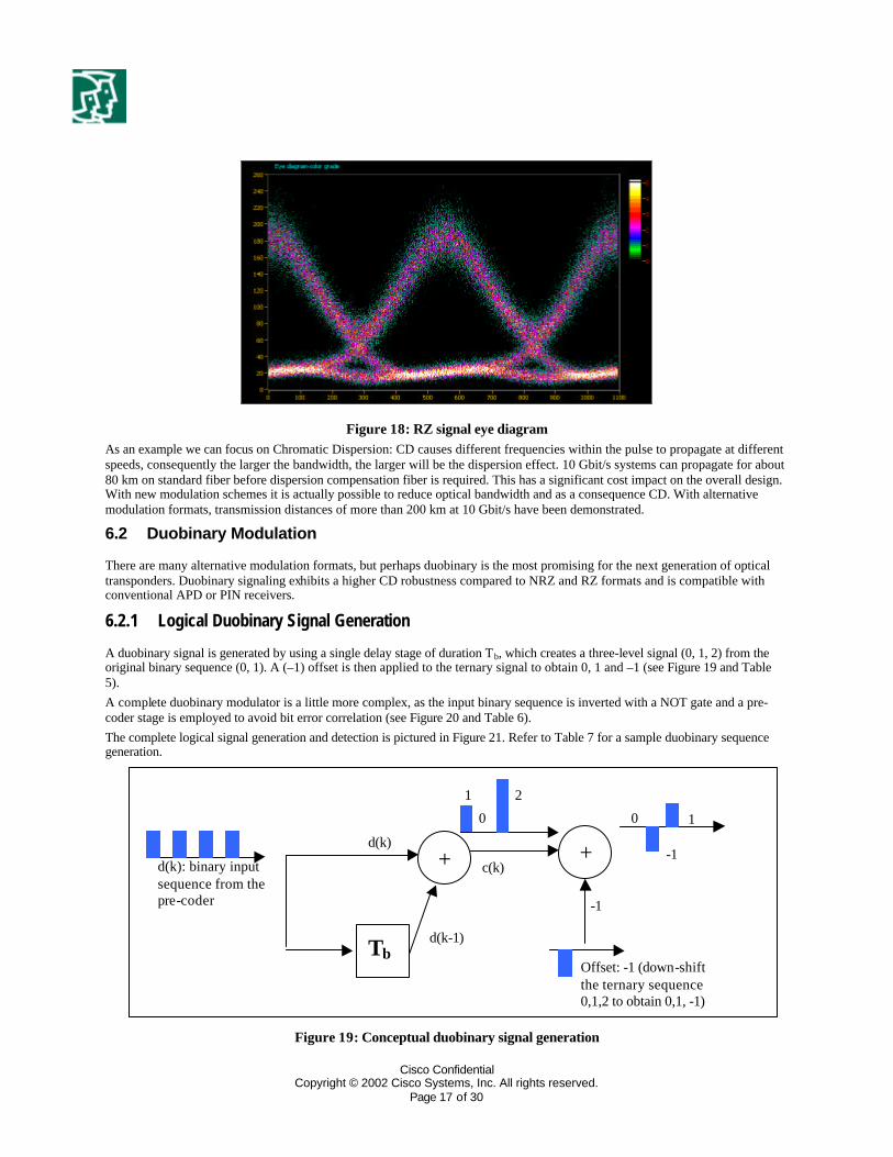
Figure 18: RZ signal eye diagram As an example we can focus on Chromatic Dispersion: CD causes different frequencies within the pulse to propagate at different speeds, consequently the larger the bandwidth, the larger will be the dispersion effect. 10 Gbit/s systems can propagate for about 80 km on standard fiber before dispersion compensation fiber is required. This has a significant cost impact on the overall design. With new modulation schemes it is actually possible to reduce optical bandwidth and as a consequence CD. With alternative modulation formats, transmission distances of more than 200 km at 10 Gbit/s have been demonstrated.
6.2 Duobinary Modulation
There are many alternative modulation formats, but perhaps duobinary is the most promising for the next generation of optical transponders. Duobinary signaling exhibits a higher CD robustness compared to NRZ and RZ formats and is compatible with conventional APD or PIN receivers.
6.2.1 Logical Duobinary Signal Generation
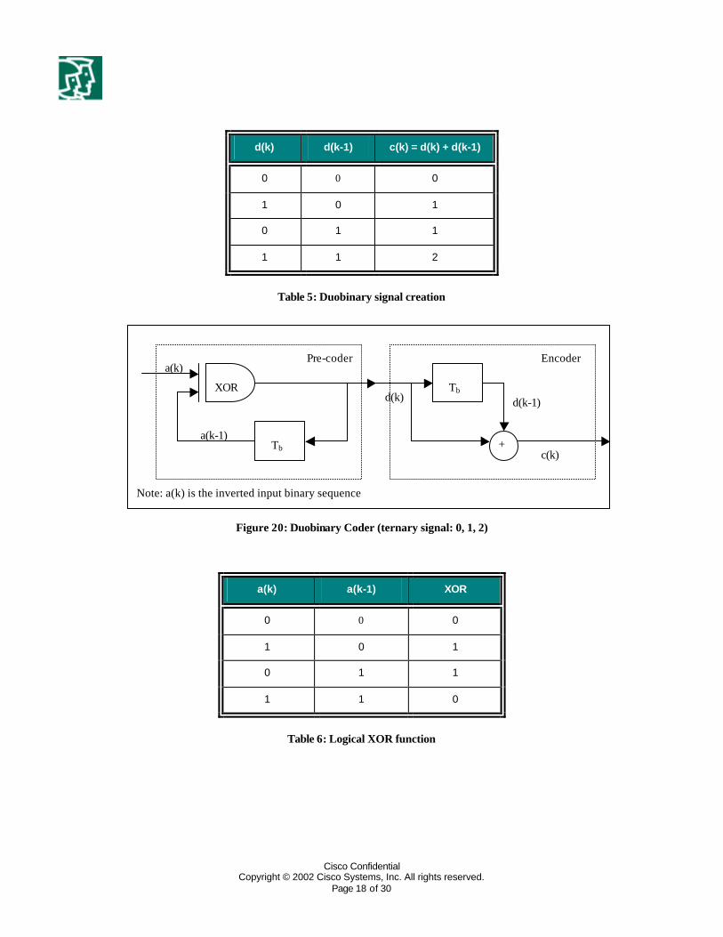
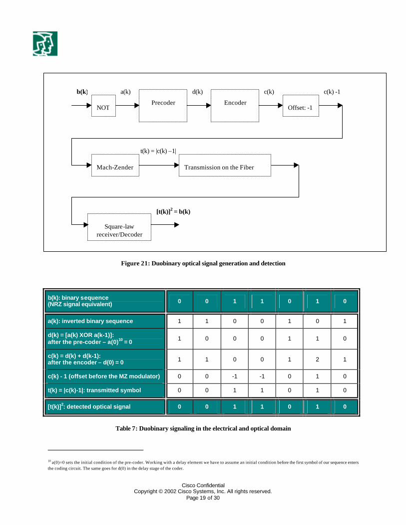
A duobinary signal is generated by using a single delay stage of duration Tb, which creates a three-level signal (0, 1, 2) from the original binary sequence (0, 1). A (–1) offset is then applied to the ternary signal to obtain 0, 1 and –1 (see Figure 19 and Table 5). A complete duobinary modulator is a little more complex, as the input binary sequence is inverted with a NOT gate and a pre-coder stage is employed to avoid bit error correlation (see Figure 20 and Table 6). The complete logical signal generation and detection is pictured in Figure 21. Refer to Table 7 for a sample duobinary sequence generation.
Figure 19: Conceptual duobinary signal generation
Offset: -1 (down-shift the ternary sequence 0,1,2 to obtain 0,1, -1)
-1
1 0
+
-1
+
Tb
d(k): binary input sequence from the pre-coder
d(k-1)
d(k)
0
1 2
c(k)
Cisco Confidential Copyright © 2002 Cisco Systems, Inc. All rights reserved.
Page 18 of 30
d(k) d(k-1) c(k) = d(k) + d(k-1)
0 0 0
1 0 1
0 1 1
1 1 2
Table 5: Duobinary signal creation
Figure 20: Duobinary Coder (ternary signal: 0, 1, 2)
a(k) a(k-1) XOR
0 0 0
1 0 1
0 1 1
1 1 0
Table 6: Logical XOR function
Tb
XOR
Pre-coder Encoder
Tb
+
a(k)
a(k-1)
d(k) d(k-1)
c(k)
Note: a(k) is the inverted input binary sequence
Cisco Confidential Copyright © 2002 Cisco Systems, Inc. All rights reserved.
Page 19 of 30
Figure 21: Duobinary optical signal generation and detection
b(k): binary sequence (NRZ signal equivalent) 0 0 1 1 0 1 0
a(k): inverted binary sequence 1 1 0 0 1 0 1
d(k) = [a(k) XOR a(k-1)]: after the pre-coder – a(0)10 = 0 1 0 0 0 1 1 0
c(k) = d(k) + d(k-1): after the encoder – d(0) = 0 1 1 0 0 1 2 1
c(k) - 1 (offset before the MZ modulator) 0 0 -1 -1 0 1 0
t(k) = |c(k)-1|: transmitted symbol 0 0 1 1 0 1 0
[t(k)]2: detected optical signal 0 0 1 1 0 1 0
Table 7: Duobinary signaling in the electrical and optical domain
10 a(0)=0 sets the initial condition of the pre-coder. Working with a delay element we have to assume an initial condition before the first symbol of our sequence enters the coding circuit. The same goes for d(0) in the delay stage of the coder.
[t(k)]2 = b(k)
NOT
b(k)
Precoder
a(k) d(k) c(k)
Encoder
c(k) -1
Offset: -1
t(k) = |c(k) –1|
Mach-Zender Transmission on the Fiber
Square-law receiver/Decoder

Cisco Confidential Copyright © 2002 Cisco Systems, Inc. All rights reserved.
Page 20 of 30
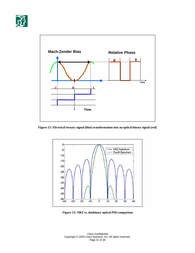
6.2.2 Duobinary Signaling in the optical domain
In the optical domain the three electric levels (0, +1 and –1) translate to only two optical levels (logical 0 and 1); using the Mach-Zender with a three-level driving voltage results in a two-levels optical signal (refer to Figure 22): the modulator “off” state corresponds to a zero, while the symbols 1 and -1 are represented by the “on” state with phase 0 and π respectively11. In Table 7 note how the NRZ signal, or the initial binary sequence, is equivalent to the optical signal at the receiver. This means that a standard receiver (a square-law device PIN or APD) is required to detect the signal. The ability to operate with “conventional” photodetectors is one of the major advantages offered by duobinary modulation compared to other advanced12 modulation schemes. Practical Duobinary implementations adopt sort of pulse shaping or electrical filtering13 (see Chapter 6.2.3). The electrical filtering considerably compresses the PSD compared to an NRZ signal (see Figure 23). The advantages of the duobinary spectrum (over NRZ) are:
• As a result of the spectrum compression, a four-fold increase in the CD tolerance compared to a standard NRZ format has been demonstrated. (Experimental 10 Gbit/s transmission distances up to 225 km on standard SMF have been reported using duobinary modulation).
• By reducing the spectral width of the signal it is possible to increase the spectral efficiency (by reducing the channel spacing, or by increasing the modulation bandwidth of the individual channels), without incurring in large penalties associated with the larger NRZ spectrum.
• The Duobinary spectrum has ideally a null DC component (removed by the filtering), hence making the signal more tolerant to Stimulated Brillouin Scattering (SBS). (The NRZ format has instead a significant amount of power associated with the DC component, see Figure 15).
11 The MZ encodes the +1 and –1 in the phase of the electric field of the optical signal. In this perspective duobinary is a form of PSK , however the receiver detects just the power of the electric field of the optical signal exactly like in classic ASK modulation (NRZ, RZ).
12 By advanced we mean various PSK flavors, like DPSK or BPSK. These formats require a “coherent” detection of the s ignal, or in other word the ability to detect the phase of the electrical field of the optical signal.
13 Basically the high-pass filter cuts the DC components, while the low-pass filters removes the side lobes and compresses the main lobe.
Cisco Confidential Copyright © 2002 Cisco Systems, Inc. All rights reserved.
Page 21 of 30
π 0
Relative Phase
-1 0 1
Time
Time
Mach-Zender Bias
Figure 22: Electrical ternary signal (blue) transformation into an optical binary signal (red)
Figure 23: NRZ vs. duobinary optical PSD comparison
Cisco Confidential Copyright © 2002 Cisco Systems, Inc. All rights reserved.
Page 22 of 30
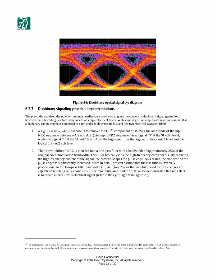
Figure 24: Duobinary optical signal eye diagram
6.2.3 Duobinary signaling practical implementations
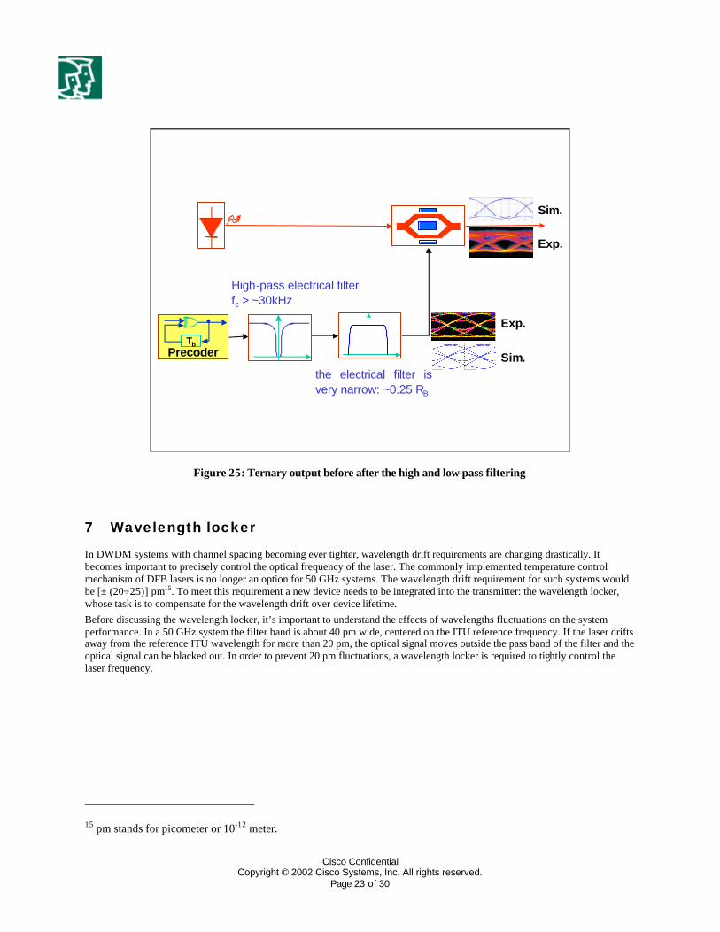
The pre-coder and de-coder schemes presented earlier are a good way to grasp the concept of duobinary signal generation, however real-life coding is achieved by means of simple electrical filters. With some degree of simplification we can assume that a duobinary coding engine is composed of a pre-coder to de-correlate bits and just two electrical cascaded filters:
1. A high-pass filter, whose purpose is to remove the DC14 component or shifting the amplitude of the input NRZ sequence between –A/2 and A/2. (The input NRZ sequence has a logical ‘0’ at the ‘0 volt’ level, while the logical ‘1’ at the ’A volt’ level. After the high-pass filter the logical ‘0’ has a –A/2 level and the logical 1 a +A/2 volt level.
2. The “down-shifted” NRZ is then fed into a low-pass filter with a bandwidth of approximately 25% of the original NRZ modulation bandwidth. This filter basically cuts the high-frequency comp onents. By reducing the high-frequency content of the signal, the filter re-shapes the pulse edge. As a result, the rise time of the pulse edges is significantly increased. More in detail, we can assume that the rise time is inversely proportional to the low-pass filter bandwidth (RB in Figure 25), or that in a bit period the pulse edges are capable of reaching only about 25% of the maximum amplitude ‘A’. It can be demonstrated that net effect is to create a three-levels electrical signal (refer to the eye diagram in Figure 25).
14 The amplitude of the original NRZ sequence is between 0 and A. This means that the average of the signal or its DC component is A/2. By filtering the DC component out the signal has null DC component or its average amplitude is now 0. The net effect is to shift the signal from [0, A] to [-A/2, +A/2].
Cisco Confidential Copyright © 2002 Cisco Systems, Inc. All rights reserved.
Page 23 of 30
PrecoderTb
High-pass electrical filter fc > ~30kHz
Sim.
Exp.
Sim.
Exp.
the electrical filter is very narrow: ~0.25 RB
Figure 25: Ternary output before after the high and low-pass filtering
7 Wavelength locker
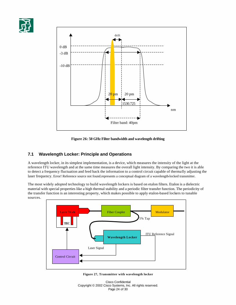
In DWDM systems with channel spacing becoming ever tighter, wavelength drift requirements are changing drastically. It becomes important to precisely control the optical frequency of the laser. The commonly implemented temperature control mechanism of DFB lasers is no longer an option for 50 GHz systems. The wavelength drift requirement for such systems would be [± (20÷25)] pm15. To meet this requirement a new device needs to be integrated into the transmitter: the wavelength locker, whose task is to compensate for the wavelength drift over device lifetime. Before discussing the wavelength locker, it’s important to understand the effects of wavelengths fluctuations on the system performance. In a 50 GHz system the filter band is about 40 pm wide, centered on the ITU reference frequency. If the laser drifts away from the reference ITU wavelength for more than 20 pm, the optical signal moves outside the pass band of the filter and the optical signal can be blacked out. In order to prevent 20 pm fluctuations, a wavelength locker is required to tightly control the laser frequency.
15 pm stands for picometer or 10-12 meter.
Cisco Confidential Copyright © 2002 Cisco Systems, Inc. All rights reserved.
Page 24 of 30
Figure 26: 50 GHz Filter bandwidth and wavelength drifting
7.1 Wavelength Locker: Principle and Operations
A wavelength locker, in its simplest implementation, is a device, which measures the intensity of the light at the reference ITU wavelength and at the same time measures the overall light intensity. By comparing the two it is able to detect a frequency fluctuation and feed back the information to a control circuit capable of thermally adjusting the laser frequency. Error! Reference source not found.represents a conceptual diagram of a wavelength-locked transmitter.
The most widely adopted technology to build wavelength lockers is based on etalon filters. Etalon is a dielectric material with special properties like a high thermal stability and a periodic filter transfer function. The periodicity of the transfer function is an interesting property, which makes possible to apply etalon-based lockers to tunable sources.
Figure 27, Transmitter with wavelength locker
1530.725
Filter band: 40pm
nm
0 dB
-3 dB
-10 dB
20 pm 20 pm
drift
Control Circuit
Wavelength Locker
Laser Diode Fiber Coupler Modulator
TEC
ITU Reference Signal
Laser Signal
5% Tap
Cisco Confidential Copyright © 2002 Cisco Systems, Inc. All rights reserved.
Page 25 of 30
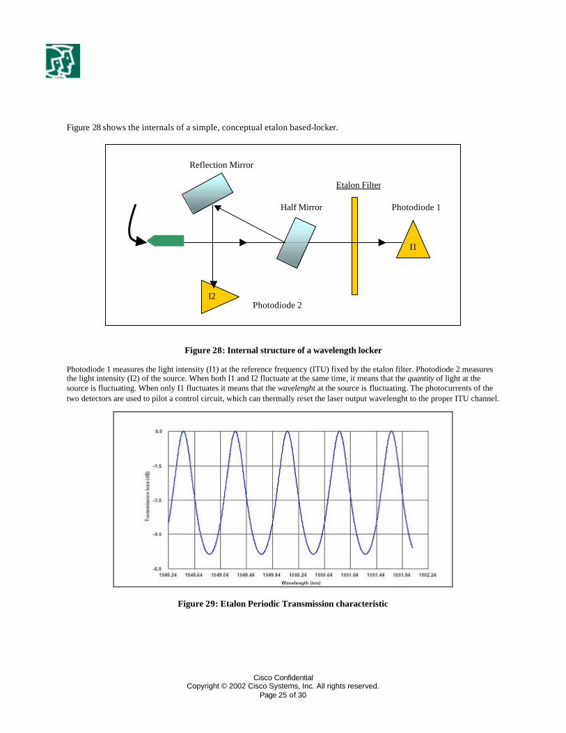
Figure 28 shows the internals of a simple, conceptual etalon based-locker.
Figure 28: Internal structure of a wavelength locker
Photodiode 1 measures the light intensity (I1) at the reference frequency (ITU) fixed by the etalon filter. Photodiode 2 measures the light intensity (I2) of the source. When both I1 and I2 fluctuate at the same time, it means that the quantity of light at the source is fluctuating. When only I1 fluctuates it means that the wavelenght at the source is fluctuating. The photocurrents of the two detectors are used to pilot a control circuit, which can thermally reset the laser output wavelenght to the proper ITU channel.
Figure 29: Etalon Periodic Transmission characteristic
Reflection Mirror
Etalon Filter
Half Mirror Photodiode 1
Photodiode 2
I1
I2
© 2003 Cisco Systems, Inc. All right reserved. Important notices, privacy statements, and trademarks of Cisco Systems, Inc. can be found on cisco.com
Page 26 of 30
8 Introduction to Forward Error Correction (FEC)
In long-haul DWDM, where systems are typically OSNR limited, a popular technique to increase the reach without penalizing BER performance, is to adopt Forward Error Correcting codes. With FEC, the transmitter appends extra bytes by means of a FEC encoder. These redundant bytes help the receiver to detect and correct corrupted bits by means of a FEC decoder. Consequently FEC enables the system to operate at a lower OSNR, while maintaining the same BER. Nowadays FEC is finding application in metro networks too because it provides the possibility to add an overhead to the signal, allowing Performance Monitoring and OAM support leaving the transported signal untouched (transparency). There are two flavors of FEC: In-band and Out-of-band. Out-of-band FEC increases the data rate by appending extra codes along with the data. In-band FEC adds the codes, but they are embedded during idle periods of the transmitted protocol. Synchronous protocols (such as SONET/SDH) have a determinate number of unused header bytes, which limits the strength of the FEC algorithm (the number of errors that can be corrected). In-band FEC protocols have the advantage of not changing the serial bit rate and can be made interoperable with non-FEC systems. Out-of-band FEC provides increased error-correction capability and is protocol-independent. Out-of-band FEC is widely used in DWDM applications, therefore in the remainder of the section we will focus on Out-of-band FEC.
8.1 FEC performance
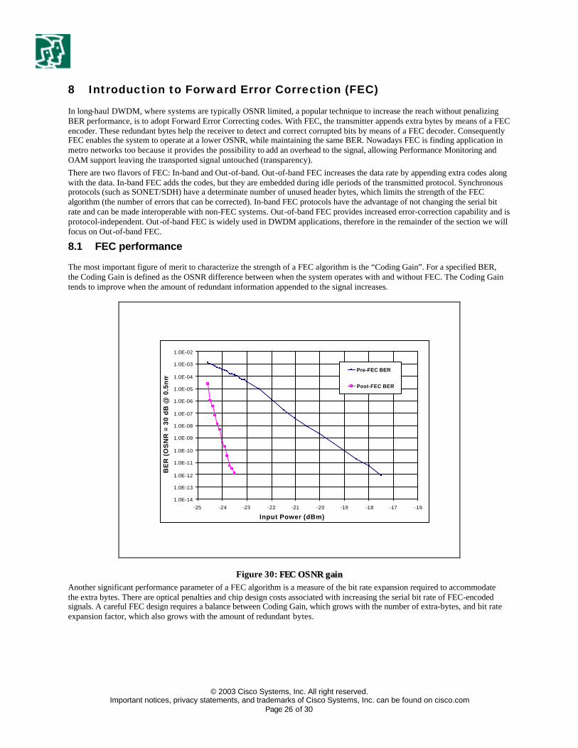
The most important figure of merit to characterize the strength of a FEC algorithm is the “Coding Gain”. For a specified BER, the Coding Gain is defined as the OSNR difference between when the system operates with and without FEC. The Coding Gain tends to improve when the amount of redundant information appended to the signal increases.
1.0E-14
1.0E-13
1.0E-12
1.0E-11
1.0E-10
1.0E-09
1.0E-08
1.0E-07
1.0E-06
1.0E-05
1.0E-04
1.0E-03
1.0E-02
-25 -24 -23 -22 -21 -20 -19 -18 -17 -16
Input Power (dBm)
BE
R (
OS
NR
= 3
0 d
B @
0.5
nm
) Pre-FEC BER
Post-FEC BER
Figure 30: FFEECC OOSS NNRR ggaaiinn Another significant performance parameter of a FEC algorithm is a measure of the bit rate expansion required to accommodate the extra bytes. There are optical penalties and chip design costs associated with increasing the serial bit rate of FEC-encoded signals. A careful FEC design requires a balance between Coding Gain, which grows with the number of extra-bytes, and bit rate expansion factor, which also grows with the amount of redundant bytes.
© 2003 Cisco Systems, Inc. All right reserved. Important notices, privacy statements, and trademarks of Cisco Systems, Inc. can be found on cisco.com
Page 27 of 30
8.2 FEC codes for Optical Communications
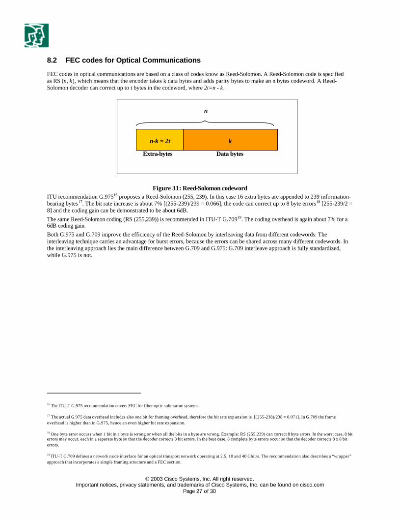
FEC codes in optical communications are based on a class of codes know as Reed-Solomon. A Reed-Solomon code is specified as RS (n, k), which means that the encoder takes k data bytes and adds parity bytes to make an n bytes codeword. A Reed-Solomon decoder can correct up to t bytes in the codeword, where 2t=n - k.
Figure 31: Reed-Solomon codeword ITU recommendation G.97516 proposes a Reed-Solomon (255, 239). In this case 16 extra bytes are appended to 239 information-bearing bytes17. The bit rate increase is about 7% [(255-239)/239 = 0.066], the code can correct up to 8 byte errors18 [255-239/2 = 8] and the coding gain can be demonstrated to be about 6dB. The same Reed-Solomon coding (RS (255,239)) is recommended in ITU-T G.70919. The coding overhead is again about 7% for a 6dB coding gain. Both G.975 and G.709 improve the efficiency of the Reed-Solomon by interleaving data from different codewords. The interleaving technique carries an advantage for burst errors, because the errors can be shared across many different codewords. In the interleaving approach lies the main difference between G.709 and G.975: G.709 interleave approach is fully standardized, while G.975 is not.
16 The ITU-T G.975 recommendation covers FEC for fiber optic submarine systems.
17 The actual G.975 data overhead includes also one bit for framing overhead, therefore the bit rate exp ansion is [(255-238)/238 = 0.071]. In G.709 the frame overhead is higher than in G.975, hence an even higher bit rate expansion.
18 One byte error occurs when 1 bit in a byte is wrong or when all the bits in a byte are wrong. Example: RS (255,239) can correct 8 byte errors. In the worst case, 8 bit errors may occur, each in a separate byte so that the decoder corrects 8 bit errors. In the best case, 8 complete byte errors occur so that the decoder corrects 8 x 8 bit errors.
19 ITU-T G.709 defines a network n ode interface for an optical transport network operating at 2.5, 10 and 40 Gbit/s. The recommendation also describes a “wrapper” approach that incorporates a simple framing structure and a FEC section.
n-k = 2t k
n
Data bytes Extra-bytes
Cisco Confidential Copyright © 2002 Cisco Systems, Inc. All rights reserved.
Page 28 of 30
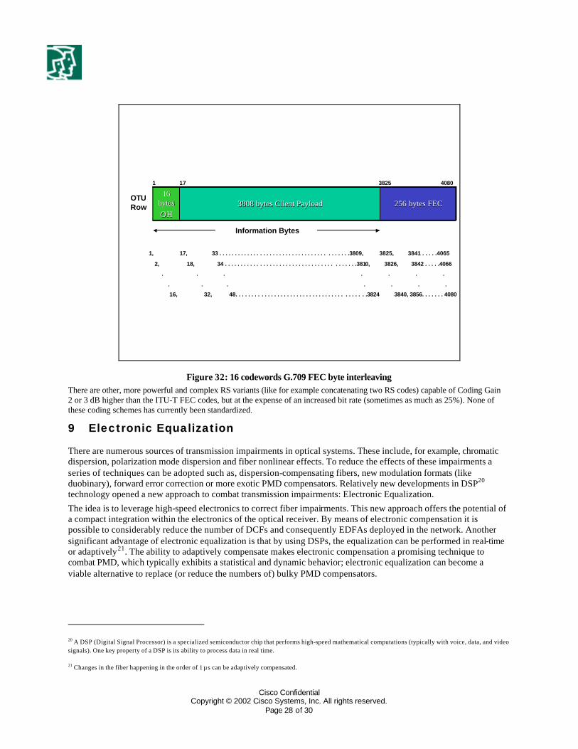
256 bytes FEC256 bytes FEC3808 bytes Client Payload3808 bytes Client Payload16 16
bytesbytesOHOH
OTU Row
1 17 3825 4080
Information Bytes
1, 17, 33 . . . . . . . . . . . . . . . . . . . . . . . . . . . . . . . . . . . . . . . . .3809, 3825, 3841 . . . . .4065
2, 18, 34 . . . . . . . . . . . . . . . . . . . . . . . . . . . . . . . . . . . . . . . . .3810, 3826, 3842 . . . . .4066
. . . . . . .
. . . . . . .
16, 32, 48. . . . . . . . . . . . . . . . . . . . . . . . . . . . . . . . . . . . . . . . .3824 3840, 3856. . . . . . . 4080
Figure 32: 16 codewords G.709 FEC byte interleaving There are other, more powerful and complex RS variants (like for example concatenating two RS codes) capable of Coding Gain 2 or 3 dB higher than the ITU-T FEC codes, but at the expense of an increased bit rate (sometimes as much as 25%). None of these coding schemes has currently been standardized.
9 Electronic Equalization
There are numerous sources of transmission impairments in optical systems. These include, for example, chromatic dispersion, polarization mode dispersion and fiber nonlinear effects. To reduce the effects of these impairments a series of techniques can be adopted such as, dispersion-compensating fibers, new modulation formats (like duobinary), forward error correction or more exotic PMD compensators. Relatively new developments in DSP20 technology opened a new approach to combat transmission impairments: Electronic Equalization.
The idea is to leverage high-speed electronics to correct fiber impairments. This new approach offers the potential of a compact integration within the electronics of the optical receiver. By means of electronic compensation it is possible to considerably reduce the number of DCFs and consequently EDFAs deployed in the network. Another significant advantage of electronic equalization is that by using DSPs, the equalization can be performed in real-time or adaptively21. The ability to adaptively compensate makes electronic compensation a promising technique to combat PMD, which typically exhibits a statistical and dynamic behavior; electronic equalization can become a viable alternative to replace (or reduce the numbers of) bulky PMD compensators.
20 A DSP (Digital Signal Processor) is a specialized semiconductor chip that performs high-speed mathematical computations (typically with voice, data, and video signals). One key property of a DSP is its ability to process data in real time.
21 Changes in the fiber happening in the order of 1 µs can be adaptively compensated.
Cisco Confidential Copyright © 2002 Cisco Systems, Inc. All rights reserved.
Page 29 of 30
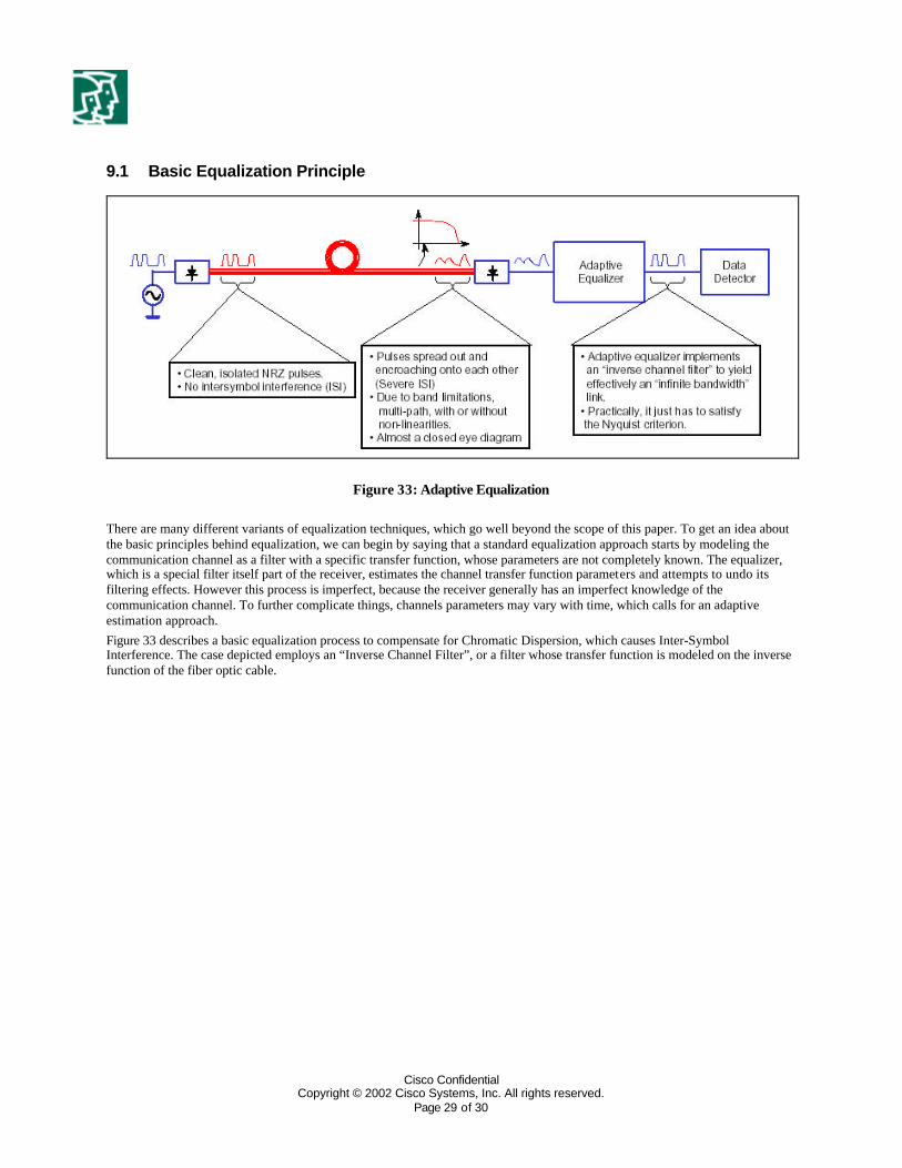
9.1 Basic Equalization Principle
Figure 33: Adaptive Equalization
There are many different variants of equalization techniques, which go well beyond the scope of this paper. To get an idea about the basic principles behind equalization, we can begin by saying that a standard equalization approach starts by modeling the communication channel as a filter with a specific transfer function, whose parameters are not completely known. The equalizer, which is a special filter itself part of the receiver, estimates the channel transfer function parameters and attempts to undo its filtering effects. However this process is imperfect, because the receiver generally has an imperfect knowledge of the communication channel. To further complicate things, channels parameters may vary with time, which calls for an adaptive estimation approach. Figure 33 describes a basic equalization process to compensate for Chromatic Dispersion, which causes Inter-Symbol Interference. The case depicted employs an “Inverse Channel Filter”, or a filter whose transfer function is modeled on the inverse function of the fiber optic cable.

© 2003 Cisco Systems, Inc. All right reserved. Important notices, privacy statements, and trademarks of Cisco Systems, Inc. can be found on cisco.com
Page 30 of 30
10 Abbreviations
APD Avalanche Photo Diode ASK Amplitude Shift Keying
BER Bit Error Rate CD Chromatic Dispersion CW Continuous Wave
DBR Distributed Bragg Reflector DC Direct Current DFB Distributed FeedBack
DSP Digital Signal Processor DWDM Dense Wavelength Division Multiplexing EA Electro-Absorption
ECL External Cavity Laser EDFA Erbium Doped Fiber Amplifier FEC Forward Error Correction
FSK Frequency Shift Keying GACC Grating Assisted Co-directional Coupler MEMS Micro Electro-Mechanical Systems
NRZ Non-Return-to-Zero OAM&P Operations, Administration, Maintenance and Performance OSNR Optical Signal Noise Ratio
PIC Photonic Integrated Circuit PMD Polarization Mode Dispersion PSD Power Spectral Densities
PSK Phase Shift Keying RF Radio Frequency RS Reed-Solomon
RZ Return-to-Zero SBS Stimulated Brillouin Scattering SG-DBR Sampled Grating Distributed Bragg Reflector
SMSR Side Mode Suppression Ratio SOA Semiconductor Optical Amplifiers VOA Variable Optical Attenuators
Copyright 2003, Cisco Systems, Inc. All rights reserved. Cisco, Cisco IOS, Cisco Systems, and the Cisco Systems logo are registered trademarks or trademarks of Cisco Systems, Inc. and/or its affiliates in the U.S. and certain other countries. All other trademarks mentioned in this document or Web site are the property of their respective owners. The use of the word partner does not imply a partnership relationship between Cisco and any other company. (0208R)