Embed Size (px)
DESCRIPTION
modem
Citation preview

c03_1 12/02/2008 91
3
AMPLIFIERS AND SIGNALPROCESSINGJohn G. Webster
Most bioelectric signals are small and require amplification. Amplifiers arealso used for interfacing sensors that sense body motions, temperature, andchemical concentrations. In addition to simple amplification, the amplifier mayalso modify the signal to produce frequency filtering or nonlinear effects. Thischapter emphasizes the operational amplifier (op amp), which has revolution-ized electronic circuit design. Most circuit design was formerly performed withdiscrete components, requiring laborious calculations, many components, andlarge expense. Now a 20-cent op amp, a few resistors, and knowledge of Ohm’slaw are all that is needed.
3.1 IDEAL OP AMPS
An op amp is a high-gain dc differential amplifier. It is normally used in circuitsthat have characteristics determined by external negative-feedback networks.
The best way to approach the design of a circuit that uses op amps is first toassume that the op amp is ideal. After the initial design, the circuit is checkedto determine whether the nonideal characteristics of the op amp are important.If they are not, the design is complete; if they are, another design check ismade, which may require additional components.
IDEAL CHARACTERISTICS
Figure 3.1 shows the equivalent circuit for a nonideal op amp. It is a dc differentialamplifier, which means that any differential voltage, vd ¼ ðv2 � v1Þ, is multipliedby the very high gain A to produce the output voltage vo.
To simplify calculations, we assume the following characteristics for anideal op amp:
1. A ¼ 1 (gain is infinity)2. vo ¼ 0, when v1 ¼ v2 (no offset voltage)
91

c03_1 12/02/2008 92
3. Rd ¼ 1 (input impedance is infinity)4. Ro ¼ 0 (output impedance is zero)5. Bandwidth = 1 (no frequency-response limitations) and no phase shift
Later in the chapter we shall examine the effect on the circuit of character-istics that are not ideal.
Figure 3.2 shows the op-amp circuit symbol, which includes two differen-tial input terminals and one output terminal. All these voltages are measuredwith respect to the ground shown. Power supplies, usually �15 V, must beconnected to terminals indicated on the manufacturer’s specification sheet(Jung, 1986; Horowitz and Hill, 1989).
TWO BASIC RULES
Throughout this chapter we shall use two basic rules (or input terminalrestrictions) that are very helpful in designing op-amp circuits.
RULE 1 When the op-amp output is in its linear range, the two input terminalsare at the same voltage.
This is true because if the two input terminals were not at the same voltage, thedifferential input voltage would be multiplied by the infinite gain to yield aninfinite output voltage. This is absurd; most op amps use a power supply of�15 V,so vo is restricted to this range. Actually the op-amp specifications guarantee a
Figure 3.1 Op-amp equivalent circuit The two inputs are vl and v2. Adifferential voltage between them causes current flow through the differentialresistance Rd. The differential voltage is multiplied by A, the gain of the opamp, to generate the output-voltage source. Any current flowing to the outputterminal vo must pass through the output resistance Ro.
Figure 3.2 Op-amp circuit symbol A voltage at v1, the inverting input, isgreatly amplified and inverted to yield vo. A voltage at v2, the noninvertinginput, is greatly amplified to yield an in-phase output at vo.
92 3 A M P L I F I E R S A N D S I G N A L P R O C E S S I N G

c03_1 12/02/2008 93
linear output range of only �10 V, although some saturate at about �13 V. Asingle supply is adequate with some op amps, such as the LM358 (Horowitz andHill, 1989).
RULE 2 No current flows into either input terminal of the op amp.
This is true because we assume that the input impedance is infinity, and nocurrent flows into an infinite impedance. Even if the input impedance werefinite, Rule 1 tells us that there is no voltage drop across Rd; so therefore, nocurrent flows.
3.2 INVERTING AMPLIFIERS
CIRCUIT
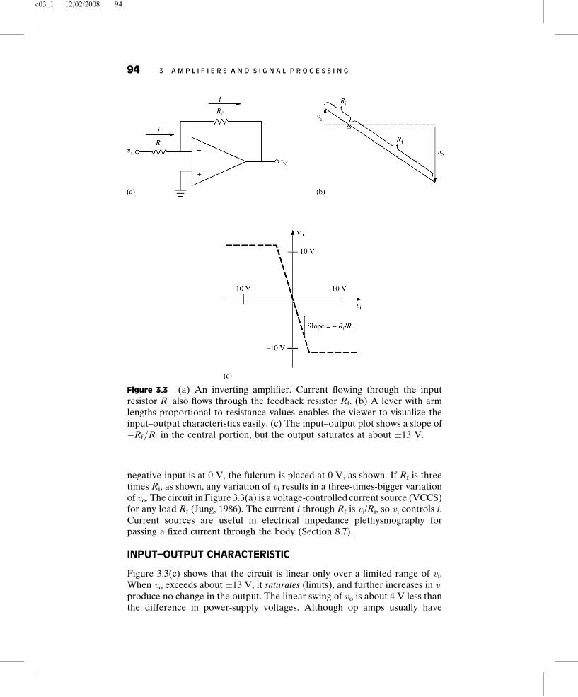
Figure 3.3(a) shows the basic inverting-amplifier circuit. It is widely used ininstrumentation. Note that a portion of vo is fed back via Rf to the negativeinput of the op amp. This provides the inverting amplifier with the manyadvantages associated with the use of negative feedback—increased band-width, lower output impedance, and so forth. If vo is ever fed back to thepositive input of the op amp, examine the circuit carefully. Either there is amistake, or the circuit is one of the rare ones in which a regenerative action isdesired.
EQUATION
Note that the positive input of the op amp is at 0 V. Therefore, by Rule 1, thenegative input of the op amp is also at 0 V. Thus no matter what happens to therest of the circuit, the negative input of the op amp remains at 0 V, a conditionknown as a virtual ground.
Because the right side of Ri, is at 0 V and the left side is vi, by Ohm’s law thecurrent i through Ri, is i ¼ vi=Ri. By Rule 2, no current can enter the op amp;therefore i must also flow through Rf. This produces a voltage drop across Rf ofiRf. Because the left end of Rf is at 0 V, the right end must be
vo ¼ �iRf ¼ �viRf
Ri
orvo
vi
¼ �Rf
Ri
(3.1)
Thus the circuit inverts, and the inverting-amplifier gain (not the op-amp gain)is given by the ratio of Rf to Ri.
LEVER ANALOGY
Figure 3.3(b) shows an easy way to visualize the circuit’s behavior. A lever isformed with arm lengths proportional to resistance values. Because the
3 . 2 I N V E R T I N G A M P L I F I E R S 93
c03_1 12/02/2008 94
negative input is at 0 V, the fulcrum is placed at 0 V, as shown. If Rf is threetimes Ri, as shown, any variation of vi results in a three-times-bigger variationof vo. The circuit in Figure 3.3(a) is a voltage-controlled current source (VCCS)for any load Rf (Jung, 1986). The current i through Rf is vi/Ri, so vi controls i.Current sources are useful in electrical impedance plethysmography forpassing a fixed current through the body (Section 8.7).
INPUT–OUTPUT CHARACTERISTIC
Figure 3.3(c) shows that the circuit is linear only over a limited range of vi.When vo exceeds about �13 V, it saturates (limits), and further increases in vi
produce no change in the output. The linear swing of vo is about 4 V less thanthe difference in power-supply voltages. Although op amps usually have
Figure 3.3 (a) An inverting amplifier. Current flowing through the inputresistor Ri also flows through the feedback resistor Rf. (b) A lever with armlengths proportional to resistance values enables the viewer to visualize theinput–output characteristics easily. (c) The input–output plot shows a slope of�Rf=Ri in the central portion, but the output saturates at about �13 V.
94 3 A M P L I F I E R S A N D S I G N A L P R O C E S S I N G

c03_1 12/02/2008 95
power-supply voltages set at �15 V, reduced power-supply voltages may beused, with a corresponding reduction in the saturation voltages and the linearswing of vo.
SUMMING AMPLIFIER
The inverting amplifier may be extended to form a circuit that yields theweighted sum of several input voltages. Each input voltage vi1, vi2, . . . , vik isconnected to the negative input of the op amp by an individual resistor theconductance of which ð1=RikÞ is proportional to the desired weighting.
EXAMPLE 3.1 The output of a biopotential preamplifier that measuresthe electro-oculogram (EOG) (Section 4.7) is an undesired dc voltage of�5 V due to electrode half-cell potentials (Section 5.1), with a desiredsignal of �1 V superimposed. Design a circuit that will balance the dcvoltage to zero and provide a gain of �10 for the desired signal withoutsaturating the op amp.
ANSWER Figure E3.1(a) shows the design. We assume that vb, the balancingvoltage available from the 5 kV potentiometer, is �10 V. The undesiredvoltage at vi ¼ 5 V. For vo ¼ 0, the current through Rf is zero. Thereforethe sum of the currents through Ri and Rb, is zero.
vi
Ri
þ vb
Rb
¼ 0
Rb ¼�Rivb
vi
¼ �104ð�10Þ5
¼ 2� 104 V
Figure E3.1 (a) This circuit sums the input voltage vi plus one-half of thebalancing voltage vb. Thus the output voltage vo can be set to zero even when vi
has a nonzero dc component, (b) The three waveforms show vi, the inputvoltage; ðvi þ vb=2Þ, the balanced-out voltage; and vo, the amplified outputvoltage. If vi were directly amplified, the op amp would saturate.
3 . 2 I N V E R T I N G A M P L I F I E R S 95

c03_1 12/02/2008 96
For a gain of �10, (3.1) requires Rf=Ri;¼ 10; or Rf;¼ 100 kV. The circuitequation is
vo ¼ �Rf
vi
Ri
þ vb
Rb
� �
vo ¼ �105 vi
104þ vb
2� 104
� �
vo ¼ �10 vi þvb
2
� �
The potentiometer can balance out any undesired voltage in the range�5 V, asshown by Figure E3.1(b). Here we have selected resistors of 10 kV to 100 kV
from the common resistors used in electronic circuits that have values between10 V and 22 MV.
3.3 NONINVERTING AMPLIFIERS
FOLLOWER
Figure 3.4(a) shows the circuit for a unity-gain follower. Because vi exists at thepositive input of the op amp, by Rule 1 vi must also exist at the negative input.But vo is also connected to the negative input. Therefore vo ¼ vi, or the outputvoltage follows the input voltage. At first glance it seems nothing is gained byusing this circuit; the output is the same as the input. However, the circuit is veryuseful as a buffer, to prevent a high source resistance from being loaded downby a low-resistance load. By Rule 2, no current flows into the positive input, andtherefore the source resistance in the external circuit is not loaded at all.
NONINVERTING AMPLIFIER
Figure 3.4(b) shows how the follower circuit can be modified to produce gain.By Rule 1, vi appears at the negative input of the op amp. This causes currenti ¼ vi=Ri, to flow to ground. By Rule 2, none of i can come from the negativeinput; therefore all must flow through Rf. We can then calculate vo ¼ iðRf þ RiÞand solve for the gain.
vo
vi
¼ iðRf þ RiÞiRi
¼ Rf þ Ri
Ri
(3.2)
We note that the circuit gain (not the op-amp gain) is positive, always greater thanor equal to 1; and that if Ri =1 (open circuit), the circuit reduces to Figure 3.4(a).
Figure 3.4(c) shows how a lever makes possible an easy visualization of theinput–output characteristics. The fulcrum is placed at the left end, because Ri isgrounded at the left end. vi appears between the two resistors, so it provides aninput at the central part of the diagram. vo travels through an output excursiondetermined by the lever arms.
96 3 A M P L I F I E R S A N D S I G N A L P R O C E S S I N G

c03_1 12/02/2008 97
Figure 3.4(d), the input–output characteristic, shows that a one-op-ampcircuit can have a positive amplifier gain. Again saturation is evident.
3.4 DIFFERENTIAL AMPLIFIERS
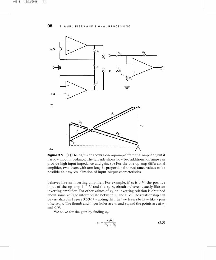
ONE-OP-AMP DIFFERENTIAL AMPLIFIER
The right side of Figure 3.5(a) shows a simple one-op-amp differential amplifier.Current flows from v4 through R3 and R4 to ground. By Rule 2, no current flowsinto the positive input of the op amp. Hence R3 and R4, act as a simple voltage-divider attenuator, which is unaffected by having the op amp attached or by anyother changes in the circuit. The voltages in this part of the circuit are visualizedin Figure 3.5(b) by the single lever that is attached to the fulcrum (ground).
By Rule 1, whatever voltage appears at the positive input also appears atthe negative input. Once this voltage is fixed, the top half of the circuit
Figure 3.4 (a) A follower, vo ¼ vi. (b) A noninverting amplifier, vi appearsacross Ri, producing a current through Ri that also flows through Rf. (c) A leverwith arm lengths proportional to resistance values makes possible an easyvisualization of input–output characteristics. (d) The input–output plot showsa positive slope of ðRf þ RiÞ=Ri in the central portion, but the output saturatesat about �13 V.
3 . 4 D I F F E R E N T I A L A M P L I F I E R S 97
c03_1 12/02/2008 98
behaves like an inverting amplifier. For example, if v4 is 0 V, the positiveinput of the op amp is 0 V and the v3–vo circuit behaves exactly like aninverting amplifier. For other values of v4, an inverting relation is obtainedabout some voltage intermediate between v4 and 0 V. The relationship canbe visualized in Figure 3.5(b) by noting that the two levers behave like a pairof scissors. The thumb and finger holes are v4 and v3, and the points are at vo
and 0 V.We solve for the gain by finding v5.
v5 ¼v4R4
R3 þ R4
(3.3)
Figure 3.5 (a) The right side shows a one-op-amp differential amplifier, but ithas low input impedance. The left side shows how two additional op amps canprovide high input impedance and gain. (b) For the one-op-amp differentialamplifier, two levers with arm lengths proportional to resistance values makepossible an easy visualization of input–output characteristics.
98 3 A M P L I F I E R S A N D S I G N A L P R O C E S S I N G

c03_1 12/02/2008 99
Then, solving for the current in the top half, we get
i ¼ v3 � v5
R3
¼ v5 � vo
R4
(3.4)
Substituting (3.3) into (3.4) yields
vo ¼ðv4 � v3ÞR4
R3
(3.5)
This is the equation for a differential amplifier. If the two inputs are hookedtogether and driven by a common source, with respect to ground, then thecommon-mode voltage vc is v3 ¼ v4. Equation (3.5) shows that the ideal outputis 0. The differential amplifier-circuit (not op-amp) common-mode gain Gc is 0.In Figure 3.5(b), imagine the scissors to be closed. No matter how the inputsare varied, vo ¼ 0.
If on the other hand v3 6¼ v4, then the differential voltage ðv4 � v3Þproduces an amplifier-circuit (not op-amp) differential gain Gd that from(3.5) is equal to R4=R3. This result can be visualized in Figure 3.5(b) by notingthat as the scissors open, vo is geometrically related to ðv4 � v3Þ in the sameratio as the lever arms, R4=R3.
No differential amplifier perfectly rejects the common-mode voltage. Toquantify this imperfection, we use the term common-mode rejection ratio(CMRR), which is defined as
CMRR ¼ Gd
Gc
(3.6)
This factor may be lower than 100 for some oscilloscope differential amplifiersand higher than 10,000 for a high-quality biopotential amplifier.
EXAMPLE 3.2 A blood-pressure sensor uses a four-active-arm Wheatstonestrain gage bridge excited with dc. At full scale, each arm changes resistanceby �0.3%. Design an amplifier that will provide a full-scale output over theop amp’s full range of linear operation. Use the minimal number ofcomponents.
ANSWER From (2.6), Dvo ¼ viDR=R ¼ 5 Vð0:003Þ ¼ 0:015 V. Gain ¼ 20=0:015 ¼ 1333. Assume R ¼ 120 V. Then the Thevenin source impedance¼ 60 V. Use this to replace R3 of Figure 3.5(a) right side. Then R4 ¼R3ðgainÞ ¼ 60 Vð1333Þ ¼ 80 kV.
THREE-OP-AMP DIFFERENTIAL AMPLIFIER
The one-op-amp differential amplifier is quite satisfactory for low-resistancesources, such as strain-gage Wheatstone bridges (Section 2.3). But the input
3 . 4 D I F F E R E N T I A L A M P L I F I E R S 99

c03_1 12/02/2008 100
resistance is too low for high-resistance sources. Our first recourse is to add thesimple follower shown in Figure 3.4(a) to each input. This provides therequired buffering. Because this solution uses two additional op amps, wecan also obtain gain from these buffering amplifiers by using a noninvertingamplifier, as shown in Figure 3.4(b). However, this solution amplifies thecommon-mode voltage, as well as the differential voltage, so there is noimprovement in CMRR.
A superior solution is achieved by hooking together the two Ri’s of thenoninverting amplifiers and eliminating the connection to ground. The result isshown on the left side of Figure 3.5(a). To examine the effects of common-modevoltage, assume that v1 ¼ v2. By Rule 1, v1, appears at both negative inputs to theop amps. This places the same voltage at both ends of R1 . Hence current throughR1 is 0. By Rule 2, no current can flow from the op-amp inputs. Hence the currentthrough both R2’s is 0, so v1 appears at both op-amp outputs and the Gc is 1.
To examine the effects when v1 6¼ v2, we note that v1 � v2 appears acrossR1. This causes a current to flow through R1 that also flows through the resistorstring R2, R1, R2. Hence the output voltage
v3 � v4 ¼ iðR2 þ R1 þ R2Þ
whereas the input voltage
v1 � v2 ¼ iR1
The differential gain is then
Gd ¼v3 � v4
v1 � v2
¼ 2R2 þ R1
R1
(3.7)
Since the Gc is 1, the CMRR is equal to the Gd, which is usually much greaterthan 1. When the left and right halves of Figure 3.5(a) are combined, theresulting three-op-amp amplifier circuit is frequently called an instrumentationamplifier. It has high input impedance, a high CMRR, and a gain that can bechanged by adjusting R1. This circuit finds wide use in measuring biopotentials(Section 6.7), because it rejects the large 60 Hz common-mode voltage thatexists on the body.
3.5 COMPARATORS
SIMPLE
A comparator is a circuit that compares the input voltage with some referencevoltage. The comparator’s output flips from one saturation limit to the other, asthe negative input of the op amp passes through 0 V. For vi greater than thecomparison level, vo ¼ �13 V. For vi less than the comparison level,
100 3 A M P L I F I E R S A N D S I G N A L P R O C E S S I N G

c03_1 12/02/2008 101
vo ¼ þ13 V. Thus this circuit performs the same function as a Schmitt trigger,which detects an analog voltage level and yields a logic level output. Thesimplest comparator is the op amp itself, as shown in Figure 3.2. If a referencevoltage is connected to the positive input and vi is connected to the negativeinput, the circuit is complete. The inputs may be interchanged to invertthe output. The input circuit may be expanded by adding the two R1 resistorsshown in Figure 3.6(a). This provides a known input resistance for the circuitand minimizes overdriving the op-amp input. Figure 3.6(b) shows that thecomparator flips when vi ¼ �vref. To avoid building a separate power supplyfor vref, we can connect vref to the�15 V power supply and adjust the values ofthe input resistors so that the negative input of the op amp is at 0 V when vi is atthe desired positive comparison level. When negative comparison levels aredesired, vref is connected to the þ15 V power supply.
WITH HYSTERESIS
For a simple comparator, if vi is at the comparison level and there is noise on vi,then vo fluctuates wildly. To prevent this, we can add hysteresis to thecomparator by adding R2 and R3, as shown in Figure 3.6(a). The effect ofthis positive feedback is illustrated by the input–output characteristics shownin Figure 3.6(b). To analyze this circuit, first assume that vref ¼ �5 V andvi ¼ þ10 V. Then, because the op amp inverts and saturates, vo ¼ �13 V.Divide vo by R2 and R3 so that the positive input is at, say, �1 V. As vi islowered, the comparator does not flip until vi reaches þ3 V, which makes thenegative input equal to the positive input,�1 V. At this point, vo flips toþ13 V,causing the positive input to change toþ1 V. Noise on vi cannot cause vo to flipback, because the negative input must be raised to þ1 V to cause the next flip.This requires vi to be raised to þ7 V, at which level the circuit can flip back toits original state. From this example, we see that the width of the hysteresis isfour times as great as the magnitude of the voltage across R3. The width of thehysteresis loop can be varied by replacing R3 by a potentiometer.
Figure 3.6 (a) Comparator. When R3 ¼ 0; vo indicates whether ðvI þ vrefÞ isgreater or less than 0 V. When R3 is larger, the comparator has hysteresis, asshown in, (b) the input–output characteristic.
3 . 5 C O M P A R A T O R S 101
c03_1 12/02/2008 102
3.6 RECTIFIERS
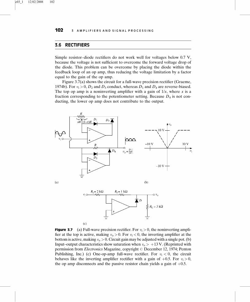
Simple resistor–diode rectifiers do not work well for voltages below 0.7 V,because the voltage is not sufficient to overcome the forward voltage drop ofthe diode. This problem can be overcome by placing the diode within thefeedback loop of an op amp, thus reducing the voltage limitation by a factorequal to the gain of the op amp.
Figure 3.7(a) shows the circuit for a full-wave precision rectifier (Graeme,1974b). For vi > 0, D2 and D3 conduct, whereas D1 and D4 are reverse-biased.The top op amp is a noninverting amplifier with a gain of 1/x, where x is afraction corresponding to the potentiometer setting. Because D4 is not con-ducting, the lower op amp does not contribute to the output.
Figure 3.7 (a) Full-wave precision rectifier. For vi > 0, the noninverting ampli-fier at the top is active, making vo > 0. For vi < 0, the inverting amplifier at thebottom is active, making vo > 0. Circuit gain may be adjusted with a single pot. (b)Input–output characteristics show saturation when vo > þ13 V. (Reprinted withpermission from Electronics Magazine, copyright # December 12, 1974; PentonPublishing, Inc.) (c) One-op-amp full-wave rectifier. For vi < 0, the circuitbehaves like the inverting amplifier rectifier with a gain of þ0.5. For vi > 0,the op amp disconnects and the passive resistor chain yields a gain of þ0.5.
102 3 A M P L I F I E R S A N D S I G N A L P R O C E S S I N G
c03_1 12/02/2008 103
For vi < 0; D1 and D4 conduct, while D2 and D3 are reverse-biased. At thepotentiometer wiper vi serves as the input to the lower op-amp invertingamplifier, which has a gain of�1=x. Because D2 is not conducting, the upper opamp does not contribute to the output. And because the polarity of the gainswitches with the polarity of vi, vo ¼ jvi=xj.
The advantage of this circuit over other full-wave rectifier circuits (Wait,1975, p. 173) is that the gain can be varied with a single potentiometer and theinput resistance is very high. If only a half-wave rectifier is needed, either thenoninverting amplifier or the inverting amplifier can be used separately, thusrequiring only one op amp. The perfect rectifier is frequently used with anintegrator to quantify the amplitude of electromyographic signals (Section 6.8).
Figure 3.7(c) shows a one-op-amp full-wave rectifier (Tompkins andWebster, 1988). Unlike other full-wave rectifiers, it requires the load to remainconstant, because the gain is a function of load.
3.7 LOGARITHMIC AMPLIFIERS
The logarithmic amplifier makes use of the nonlinear volt–ampere relation ofthe silicon planar transistor (Jung, 1986).
VBE ¼ 0:060 logIC
IS
� �(3.8)
where
VBE ¼ base� emitter voltage
IC ¼ collector current
IS ¼ reverse saturation current; 10�13A at 27 �C
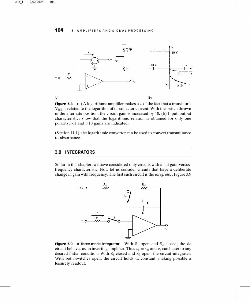
The transistor is placed in the transdiode configuration shown in Figure3.8(a), in which IC ¼ vi=Ri. Then the output vo ¼ VBE is logarithmically relatedto vi as given by (3.8) over the approximate range 10�7 A< IC < 10�2 A. Theapproximate range of vo is �0.36 to �0.66 V, so larger ranges of vo aresometimes obtained by the alternate switch position shown in Figure 3.8(a).The resistor network feeds back only a fraction of vo in order to boost vo anduses the same principle as that used in the noninverting amplifier. Figure 3.8(b)shows the input–output characteristics for each of these circuits.
Because semiconductors are temperature sensitive, accurate circuits re-quire temperature compensation. Antilog (exponential) circuits are made byinterchanging the resistor and semiconductor. These log and antilog circuitsare used to multiply a variable, divide it, or raise it to a power; to compresslarge dynamic ranges into small ones; and to linearize the output of deviceswith logarithmic or exponential input-output relations. In the photometer
3 . 7 L O G A R I T H M I C A M P L I F I E R S 103
c03_1 12/02/2008 104
(Section 11.1), the logarithmic converter can be used to convert transmittanceto absorbance.
3.8 INTEGRATORS
So far in this chapter, we have considered only circuits with a flat gain-versus-frequency characteristic. Now let us consider circuits that have a deliberatechange in gain with frequency. The first such circuit is the integrator. Figure 3.9
Figure 3.8 (a) A logarithmic amplifier makes use of the fact that a transistor’sVBE is related to the logarithm of its collector current. With the switch thrownin the alternate position, the circuit gain is increased by 10. (b) Input–outputcharacteristics show that the logarithmic relation is obtained for only onepolarity; �1 and �10 gains are indicated.
Figure 3.9 A three-mode integrator With S1 open and S2 closed, the dccircuit behaves as an inverting amplifier. Thus vo ¼ vic and vo can be set to anydesired initial condition. With S1 closed and S2 open, the circuit integrates.With both switches open, the circuit holds vo constant, making possible aleisurely readout.
104 3 A M P L I F I E R S A N D S I G N A L P R O C E S S I N G

c03_1 12/02/2008 105
shows the circuit for an integrator, which is obtained by closing switch Si. Thevoltage across an initially uncharged capacitor is given by
v ¼ 1
C
Z t1
0
idt (3.9)
where i is the current through C and t1 is the integration time. For theintegrator, for vi positive, the input current i ¼ vi=R flows through C in adirection to cause vo to move in a negative direction. Thus
vo ¼ �1
RC
Z t1
0
vidt þ vic (3.10)
This shows that vo is equal to the negative integral of vi, scaled by the factor 1/RC and added to vic, the voltage due to the initial condition. For vo ¼ 0 andvi ¼ constant; vo ¼ �vi after an integration time equal to RC. Because any realintegrator eventually drifts into saturation, a means must be provided torestore vo to any desired initial condition. If an initial condition of vo ¼ 0 Vis desired, a simple switch to short out C is sufficient. For more versatility, S1 isopened and S2 closed. This dc circuit then acts as an inverting amplifier, whichmakes vo ¼ vic. During integration, S1 is closed and S2 open. After theintegration, both switches may be opened to hold the output at the finalcalculated value, thus permitting time for a readout. The circuit is useful forcomputing the area under a curve, as technicians do when they calculatecardiac output (Section 8.2).
The frequency response of an integrator is easily analyzed because theformula for the inverting amplifier gain (3.1) can be generalized to any inputand feedback impedances. Thus for Figure 3.9, with S1 closed,
Voð jvÞVið jvÞ
¼ Zf
Zi
¼ � 1= jvC
R
¼ � 1
jvRC¼ � 1
jvt
(3.11)
where t ¼ RC; v ¼ 2pf , and f = frequency. Equation (3.11) shows that thecircuit gain decreases as R increases, Figure 3.10 shows the frequency response,and (3.11) shows that the circuit gain is 1 when vt ¼ 1.
EXAMPLE 3.3 The output of the piezoelectric sensor shown in Figure2.11(b) may be fed directly into the negative input of the integrator shown inFigure 3.9, as shown in Figure E3.2. Analyze the circuit of this chargeamplifier and discuss its advantages.
ANSWER Because the FET-op-amp negative input is a virtual ground, isC ¼isR ¼ 0. Hence long cables may be used without changing sensor sensitivity or
3 . 8 I N T E G R A T O R S 105

c03_1 12/02/2008 106
time constant, as is the case with voltage amplifiers. From Figure E3.2, currentgenerated by the sensor, is ¼ K dx=dt, all flows into C, so, using (3.10), we findthat vo is
vo ¼ �v � 1
C
Z t1
0
Kdx
dtdt ¼ � kX
C
which shows that vo is proportional to x, even down to dc. Like theintegrator, the charge amplifier slowly drifts with time because of bias
Figure E3.2 The charge amplifier transfers charge generated from a piezo-electric sensor to the op-amp feedback capacitor C.
Figure 3.10 Bode plot (gain versus frequency) for various filters Integrator(I); differentiator (D); low pass (LP), 1, 2, 3 section (pole); high pass (HP);bandpass (BP). Corner frequencies fc for high-pass, low-pass, and bandpassfilters.
106 3 A M P L I F I E R S A N D S I G N A L P R O C E S S I N G

c03_1 12/02/2008 107
currents required by the op-amp input. A large feedback resistance Rmust therefore be added to prevent saturation. This causes the circuit tobehave as a high-pass filter, with a time constant t ¼ RC. It then respondsonly to frequencies above fc ¼ 1=ð2pRCÞ and has no frequency-responseimprovement over the voltage amplifier. Common capacitor values are10 pF to 1 mF.
3.9 DIFFERENTIATORS
Interchanging the integrator’s R and C yields the differentiator shown inFigure 3.11. The current through a capacitor is given by
i ¼ Cdv
dt(3.12)
If dvi=dt is positive, i flows through R in a direction such that it yields a negativevo. Thus
vo ¼ �RCdvi
dt(3.13)
The frequency response of a differentiator is given by the ratio of feedbackto input impedance.
Voð jvÞVið jvÞ
¼ �Zf
Zi
¼ � R
1= jvC
¼ � jvRC ¼ � jvt (3.14)
Equation (3.14) shows that the circuit gain increases as f increases and that it isequal to unity when vt ¼ 1. Figure 3.10 shows the frequency response.
Unless specific preventive steps are taken, the circuit tends to oscillate.The output also tends to be noisy, because the circuit emphasizes highfrequencies. A differentiator followed by a comparator is useful for detecting
Figure 3.11 A differentiator The dashed lines indicate that a small capacitormust usually be added across the feedback resistor to prevent oscillation.
3 . 9 D I F F E R E N T I A T O R S 107

c03_1 12/02/2008 108
an event the slope of which exceeds a given value—for example, detection ofthe R wave in an electrocardiogram.
3.10 ACTIVE FILTERS
LOW-PASS FILTER
Figure 1.9(a) shows a low-pass filter that is useful for attenuating high-frequency noise. A low-pass active filter can be obtained by using the one-op-amp circuit shown in Figure 3.12(a). The advantages of this circuit are that
Figure 3.12 Active filters (a) A low-pass filter attenuates high frequencies.(b) A high-pass filter attenuates low frequencies and blocks dc. (c) A bandpassfilter attenuates both low and high frequencies.
108 3 A M P L I F I E R S A N D S I G N A L P R O C E S S I N G

c03_1 12/02/2008 109
it is capable of gain and that it has a very low output impedance. The frequencyresponse is given by the ratio of feedback to input impedance.
Voð jvÞVið jvÞ
¼ �Zf
Zi
¼ �
ðRf= jvCfÞ½ð1= jvCfÞ þ Rf�
Ri
¼ Rf
ð1þ jvRfCfÞRi
¼ �Rf
Ri
1
1þ jvt (3.15)
where t ¼ RfCf. Note that (3.15) has the same form as (1.23). Figure 3.10 showsthe frequency response, which is similar to that shown in Figure 1.8(d). Forv� 1=t, the circuit behaves as an inverting amplifier (Figure 3.3), because theimpedance of Cf is large compared with Rf. For v� 1=t, the circuit behaves asan integrator (Figure 3.9), because Cf is the dominant feedback impedance.The corner frequency fc, which is defined by the intersection of the twoasymptotes shown, is given by the relation vt ¼ 2pfct ¼ 1. When a designerwishes to limit the frequency of a wide-bandwideband amplifier, it is notnecessary to add a separate stage, as shown in Figure 3.12(a), but only to addthe correct size Cf to the existing wide-band amplifier.
HIGH-PASS FILTER
Figure 3.12(b) shows a one-op-amp high-pass filter. Such a circuit is useful foramplifying a small ac voltage that rides on top of a large dc voltage, because Ci,blocks the dc. The frequency-response equation is
Voð jvÞVið jvÞ
¼ �Zf
Zi
¼ � Rf
1= jvCi þ Ri
¼ � jvRfCi
1þ jvCiRi
¼ �Rf
Ri
jvt
1þ jvt (3.16)
where t ¼ RiCi. Figure 3.10 shows the frequency response. For v� 1=t, thecircuit behaves as a differentiator (Figure 3.11), because Ci: is the dominantinput impedance. For v� 1=t, the circuit behaves as an inverting amplifier,because the impedance of Ri is large compared with that of Ci. The cornerfrequency fc, which is defined by the intersection of the two asymptotes shown,is given by the relation vt ¼ 2pfct ¼ 1.
BANDPASS FILTER
A series combination of the low-pass filter and the high-pass filter results in abandpass filter, which amplifies frequencies over a desired range and attenu-ates higher and lower frequencies. Figure 3.12(c) shows that the bandpassfunction can be achieved with a one-op-amp circuit. Figure 3.10 shows thefrequency response. The corner frequencies are defined by the same relationsas those for the low-pass and the high-pass filters. This circuit is useful for
3 . 1 0 A C T I V E F I L T E R S 109

c03_1 12/02/2008 110
amplifying a certain band of frequencies, such as those required for recordingheart sounds or the electrocardiogram.
3.11 FREQUENCY RESPONSE
Up until now, we have found it useful to consider the op amp as ideal. Now weshall examine the effects of several nonideal characteristics, starting with thatof frequency response.
OPEN-LOOP GAIN
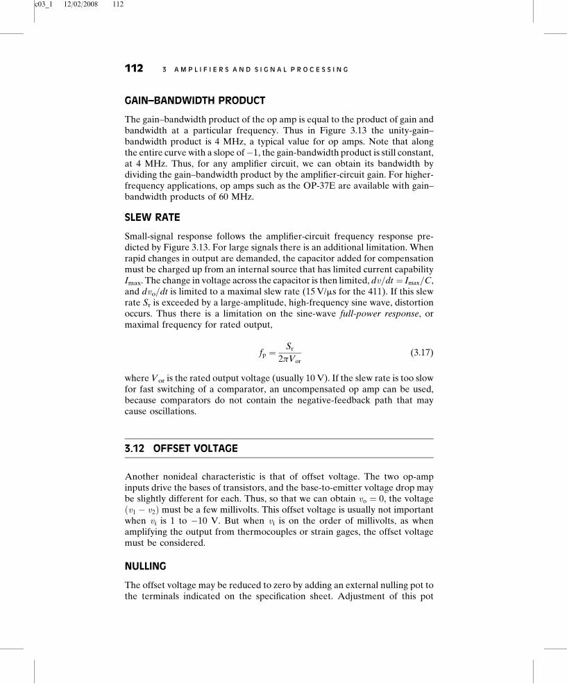
Because the op amp requires very high gain, it has several stages. Each of thesestages has stray or junction capacitance that limits its high-frequency responsein the same way that a simple RC low-pass filter reduces high-frequency gain.At high frequencies, each stage has a �1 slope on a log–log plot of gain versusfrequency, and each has a�908 phase shift. Thus a three-stage op amp, such astype 709, reaches a slope of �3, as shown by the dashed curve in Figure 3.13.
Figure 3.13 Op-amp frequency characteristics Early op amps (such as the 709)were uncompensated, had a gain greater than 1 when the phase shift was equal to�1808, and therefore oscillated unless compensation was added externally. Apopular op amp, the 411, is compensated internally; so for a gain greater than 1,the phase shift is limited to�908. When feedback resistors are added to build anamplifier circuit, the loop gain on this log–log plot is the difference between theop-amp gain and the amplifier–circuit gain.
110 3 A M P L I F I E R S A N D S I G N A L P R O C E S S I N G

c03_1 12/02/2008 111
The phase shift reaches �2708, which is quite satisfactory for a comparator,because feedback is not employed. For an amplifier, if the gain is greater than 1when the phase shift is equal to �1808 (the closed-loop condition for oscilla-tion), there is undesirable oscillation.
COMPENSATION
Adding an external capacitor to the terminals indicated on the specificationsheet moves one of the RC filter corner frequencies to a very low frequency.This compensates the uncompensated op amp, resulting in a slope of�1 and amaximal phase shift of�908. This is done with an internal capacitor in the 411,resulting in the solid curve shown in Figure 3.13. This op amp does notoscillate for any amplifier we have described. This op amp has very high dcgain, but the gain is progressively reduced at higher frequencies, until it is only1 at 4 MHz.
CLOSED-LOOP GAIN
It might appear that the op amp has very poor frequency response, because itsgain is reduced for frequencies above 40 Hz. However, an amplifier circuit isnever built using the op-amp open loop, so we shall therefore discuss only thecircuit closed-loop response. For example, if we build an amplifier circuit witha gain of 10, as shown in Figure 3.13, the frequency response is flat up to 400kHz and is reduced above that frequency only because the amplifier-circuitgain can never exceed the op-amp gain. We find this an advantage of usingnegative feedback, in that the frequency response is greatly extended.
LOOP GAIN
The loop gain for an amplifier circuit is obtained by breaking the feedback loopat any point in the loop, injecting a signal, and measuring the gain around theloop. For example, in a unity-gain follower [Figure 3.4(a)] we break thefeedback loop and then the injected signal enters the negative input, afterwhich it is amplified by the op-amp gain. Therefore, the loop gain equals theop-amp gain. To measure loop gain in an inverting amplifier with a gain of �1[Figure 3.3(a)], assume that the amplifier-circuit input is grounded. Theinjected signal is divided by 2 by the attenuator formed of Rf and Ri, and isthen amplified by the op-amp gain. Thus the loop gain is equal to (op-ampgain)/2.
Figure 3.13 shows the loop-gain concept for a noninverting amplifier. Theamplifier-circuit gain is 10. On the log–log plot, the difference between the op-amp gain and the amplifier-circuit gain is the loop gain. At low frequencies, theloop gain is high and the closed-loop amplifier-circuit characteristics aredetermined by the feedback resistors. At high frequencies, the loop gain islow and the amplifier-circuit characteristics follow the op-amp characteristics.High loop gain is good for accuracy and stability, because the feedbackresistors can be made much more stable than the op-amp characteristics.
3 . 1 1 F R E Q U E N C Y R E S P O N S E 111
c03_1 12/02/2008 112
GAIN–BANDWIDTH PRODUCT
The gain–bandwidth product of the op amp is equal to the product of gain andbandwidth at a particular frequency. Thus in Figure 3.13 the unity-gain–bandwidth product is 4 MHz, a typical value for op amps. Note that alongthe entire curve with a slope of�1, the gain-bandwidth product is still constant,at 4 MHz. Thus, for any amplifier circuit, we can obtain its bandwidth bydividing the gain–bandwidth product by the amplifier-circuit gain. For higher-frequency applications, op amps such as the OP-37E are available with gain–bandwidth products of 60 MHz.
SLEW RATE
Small-signal response follows the amplifier-circuit frequency response pre-dicted by Figure 3.13. For large signals there is an additional limitation. Whenrapid changes in output are demanded, the capacitor added for compensationmust be charged up from an internal source that has limited current capabilityImax. The change in voltage across the capacitor is then limited, dv=dt ¼ Imax=C,and dvo=dt is limited to a maximal slew rate (15 V/ms for the 411). If this slewrate Sr is exceeded by a large-amplitude, high-frequency sine wave, distortionoccurs. Thus there is a limitation on the sine-wave full-power response, ormaximal frequency for rated output,
fp ¼Sr
2pVor
(3.17)
where Vor is the rated output voltage (usually 10 V). If the slew rate is too slowfor fast switching of a comparator, an uncompensated op amp can be used,because comparators do not contain the negative-feedback path that maycause oscillations.
3.12 OFFSET VOLTAGE
Another nonideal characteristic is that of offset voltage. The two op-ampinputs drive the bases of transistors, and the base-to-emitter voltage drop maybe slightly different for each. Thus, so that we can obtain vo ¼ 0, the voltageðv1 � v2Þ must be a few millivolts. This offset voltage is usually not importantwhen vi is 1 to �10 V. But when vi is on the order of millivolts, as whenamplifying the output from thermocouples or strain gages, the offset voltagemust be considered.
NULLING
The offset voltage may be reduced to zero by adding an external nulling pot tothe terminals indicated on the specification sheet. Adjustment of this pot
112 3 A M P L I F I E R S A N D S I G N A L P R O C E S S I N G

c03_1 12/02/2008 113
increases emitter current through one of the input transistors and lowers itthrough the other. This alters the base-to-emitter voltage of the two transistorsuntil the offset voltage is reduced to zero.
DRIFT
Even though the offset voltage may be set to 0 at 25 8C, it does not remainthere if temperature is not constant. Temperature changes that affect thebase-to-emitter voltages may be due to either environmental changes or tovariations in the dissipation of power in the chip that result from fluctuatingoutput voltage. The effects of temperature may be specified as a maximaloffset voltage change in volts per degree Celsius or a maximal offset voltagechange over a given temperature range, say�25 8C toþ85 8C. If the drift of aninexpensive op amp is too high for a given application, tighter specificationsð0:1 mV/�CÞ are available with temperature-controlled chips. An alternativetechnique modulates the dc as in chopper-stabilized and varactor op amps(Tobey et al., 1971).
NOISE
All semiconductor junctions generate noise, which limits the detection of smallsignals. Op amps have transistor input junctions, which generate both noise-voltage sources and noise-current sources. These can be modeled as shown inFigure 3.14. For low source impedances, only the noise voltage vn is important;it is large compared with the inR drop caused by the current noise in. The noiseis random, but the amplitude varies with frequency. For example, at low
Figure 3.14 Noise sources in an op amp The noise-voltage source vn is inseries with the input and cannot be reduced. The noise added by the noise-current sources in can be minimized by using small external resistances.
3 . 1 2 O F F S E T V O L T A G E 113

c03_1 12/02/2008 114
frequencies the noise power density varies as 1=f (flicker noise), so a largeamount of noise is present at low frequencies. At the midfrequencies, the noiseis lower and can be specified in root-mean-square (rms) units of V�Hz�1=2. Inaddition, some silicon planar-diffused bipolar integrated-circuit op ampsexhibit bursts of noise, called popcorn noise (Wait et al., 1975).
3.13 BIAS CURRENT
Because the two op-amp inputs drive transistors, base or gate current must flowall the time to keep the transistors turned on. This is called bias current, whichfor the 411 is about 200 pA. This bias current must flow through the feedbacknetwork. It causes errors proportional to feedback-element resistances. Tominimize these errors, small feedback resistors, such as those with resistancesof 10 kV, are normally used. Smaller values should be used only after a check todetermine that the current flowing through the feedback resistor, plus thecurrent flowing through all load resistors, does not exceed the op-amp outputcurrent rating (20 mA for the 411).
DIFFERENTIAL BIAS CURRENT
The difference between the two input bias currents is much smaller than eitherof the bias currents alone. A degree of cancellation of the effects of biascurrent can be achieved by having each bias current flow through the sameequivalent resistance. This is accomplished for the inverting amplifier and thenoninverting amplifier by adding, in series with the positive input, a compen-sation resistor the value of which is equal to the parallel combination of Ri andRf. There still is an error, but it is now determined by the difference in biascurrent.
DRIFT
The input bias currents are transistor base or gate currents, so they aretemperature sensitive, because transistor gain varies with temperature. How-ever, the changes in gain of the two transistors tend to track together, so theadditional compensation resistor that we have described minimizes theproblem.
NOISE
Figure 3.14 shows how variations in bias current contribute to overall noise.The noise currents flow through the external equivalent resistances so that thetotal rms noise voltage is
vffif½v2n þ ðinR1Þ2 þ ðinR2Þ2 þ 4kTR1 þ 4kTR2�BWg1=2 (3.18)
114 3 A M P L I F I E R S A N D S I G N A L P R O C E S S I N G
c03_1 12/02/2008 115
where
R1 and R2 ¼ equivalent source resistances
vn ¼ mean value of the rms noise voltage; in V�Hz�1=2;
across the frequency range of interest
in ¼ mean value of the rms noise current; in A�Hz�1=2;
across the frequency range of interest
k ¼ Boltzmann’s constant ðAppendixÞT ¼ temperature; K
BW ¼ noise bandwidth; Hz
The specification sheet provides values of vn and in (sometimes v2n and i2
n),thus making it possible to compare different op amps. If the source resistances are10 kV, bipolar-transistor op amps yield the lowest noise. For larger sourceresistances, low-input-current amplifiers such as the field-effect transistor (FET)input stage are best because of their lower current noise. Ary (1977) presentsdesign factors and performance specifications for a low-noise amplifier.
For ac amplifiers, the lowest noise is obtained by calculating the charac-teristic noise resistance Rn ¼ vn=in and setting it equal to the equivalent sourceresistance R2 (for the noninverting amplifier). This is accomplished by insertinga transformer with turns ratio 1 : N, where N ¼ ðRn=R2Þ1=2, between the sourceand the op amp (Jung, 1986).
3.14 INPUT AND OUTPUT RESISTANCE
INPUT RESISTANCE
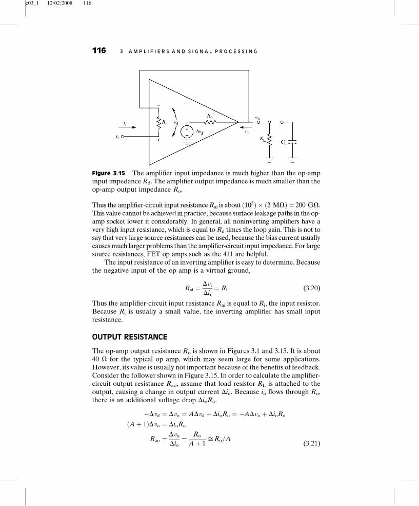
The op-amp differential-input resistance Rd is shown in Figures 3.1 and 3.15.For the FET-input 411, it is 1 TV, whereas for BJT-input op amps, it is about2 MV, which is comparable to the value of some feedback resistors used.However, we shall see that its value is usually not important because of thebenefits of feedback. Consider the follower shown in Figure 3.15. In order tocalculate the amplifier-circuit input resistance Rai, assume a change in inputvoltage vi. Because this is a follower,
Dvo ¼ ADvd ¼ AðDvi � DvoÞ
¼ ADvi
Aþ 1
Dii ¼Dvd
Rd
¼ Dvi � Dvo
Rd
¼ Dvi
ðAþ 1ÞRd
Rai ¼Dvi
Dii
¼ ðAþ 1ÞRdffiARd(3.19)
3 . 1 4 I N P U T A N D O U T P U T R E S I S T A N C E 115
c03_1 12/02/2008 116
Thus the amplifier-circuit input resistance Rai is about ð105Þ � ð2 MVÞ ¼ 200 GV.This value cannot be achieved in practice, because surface leakage paths in the op-amp socket lower it considerably. In general, all noninverting amplifiers have avery high input resistance, which is equal to Rd times the loop gain. This is not tosay that very large source resistances can be used, because the bias current usuallycauses much larger problems than the amplifier-circuit input impedance. For largesource resistances, FET op amps such as the 411 are helpful.
The input resistance of an inverting amplifier is easy to determine. Becausethe negative input of the op amp is a virtual ground,
Rai ¼Dvi
Dii
¼ Ri (3.20)
Thus the amplifier-circuit input resistance Rai is equal to Ri, the input resistor.Because Ri is usually a small value, the inverting amplifier has small inputresistance.
OUTPUT RESISTANCE
The op-amp output resistance Ro is shown in Figures 3.1 and 3.15. It is about40 V for the typical op amp, which may seem large for some applications.However, its value is usually not important because of the benefits of feedback.Consider the follower shown in Figure 3.15. In order to calculate the amplifier-circuit output resistance Rao, assume that load resistor RL is attached to theoutput, causing a change in output current Dio. Because io flows through Ro,there is an additional voltage drop DioRo.
�Dvd ¼ Dvo ¼ ADvd þ DioRo ¼ �ADvo þ DioRo
ðAþ 1ÞDvo ¼ DioRo
Rao ¼Dvo
Dio
¼ Ro
Aþ 1ffiRo=A
(3.21)
Figure 3.15 The amplifier input impedance is much higher than the op-ampinput impedance Rd. The amplifier output impedance is much smaller than theop-amp output impedance Ro.
116 3 A M P L I F I E R S A N D S I G N A L P R O C E S S I N G
c03_1 12/02/2008 117
Thus the amplifier-circuit output resistance Rao is about 40=105 ¼ 0:0004 V,a value negligible in most circuits. In general, all noninverting and inver-ting amplifiers have an output resistance that is equal to Ro divided bythe loop gain. This is not to say that very small load resistances can bedriven by the output. If RL shown in Figure 3.15 is smaller than 500 V, theop amp saturates internally, because the maximal current output for atypical op amp is 20 mA. This maximal current output must also beconsidered when driving large capacitances CL at a high slew rate. Thenthe output current
io ¼ CLdvo
dt(3.22)
The Ro�CL combination also acts as a low-pass filter, which introducesadditional phase shift around the loop and can cause oscillation. The cureis to add a small resistor between vo and CL, thus isolating CL from thefeedback loop.
To achieve larger current outputs, the current booster is used. An ordinaryop amp drives high-power transistors (on heat sinks if required). Then we canuse the entire circuit as an op amp by connecting terminals v1, v2, and vo toexternal feedback networks. This places the booster section within the feed-back loop and keeps distortion low.
3.15 PHASE-SENSITIVE DEMODULATORS
Figure 2.7 shows that a linear variable differential transformer requires aphase-sensitive demodulator to yield a useful output signal. A phase-sensitivedemodulator does not measure phase but yields a full-wave-rectified output ofthe in-phase component of a sine wave. Its output is proportional to theamplitude of the input, but it changes sign when the phase shifts by 1808.
Figure 3.16 shows the functional operation of a phase-sensitive de-modulator. Figure 3.16(a) shows a switching function that is derived from acarrier oscillator and causes the double-pole double-throw switch in Figure3.16(b) to be in the upper position for þ1 and in the lower position for �1. Ineffect, this multiplies the input signal vi by the switching function shown inFigure 3.16(a). The in-phase sine wave in Figure 3.16(c) is demodulated by thisswitch to yield the full-wave-rectified positive signal in Figure 3.16(d). The sinewave in Figure 3.16(e) is 1808 out of phase, so it yields the negative signal inFigure 3.16(f).
Amplifier stray capacitance may cause an undesirable quadrature voltagethat is shifted 908, as shown in Figure 3.16(g). The demodulated signal in Figure3.16(h) averages to zero when passed through a low-pass filter and is rejected.The dc signal shown in Figure 3.16(i) is demodulated to the wave shown inFigure 3.16(j) and is rejected. Any frequency component not locked to the
3 . 1 5 P H A S E - S E N S I T I V E D E M O D U L A T O R S 117

c03_1 12/02/2008 118
carrier frequency is similarly rejected. Because the phase-sensitive de-modulator has excellent noise-rejection capabilities, it is frequently used todemodulate the suppressed-carrier waveforms obtained from linear variabledifferential transformers (LVDTs) and the ac-excited strain-gage Wheatstonebridge (Section 2.3). A carrier system and phase-sensitive demodulator arealso essential for operation of the electromagnetic blood flowmeter (Section8.3). The noise-rejection capability may be improved by placing a tunedamplifier before the phase-sensitive demodulator, thus forming a lock-inamplifier (Aronson, 1977).
Figure 3.16 Functional operation of a phase-sensitive demodulator (a) Switch-ing function. (b) Switchswitch. (c), (e), (g), (i) Several several input voltages. (d),(f), (h), (j) Corresponding corresponding output voltages.
118 3 A M P L I F I E R S A N D S I G N A L P R O C E S S I N G

c03_1 12/02/2008 119
A practical phase-sensitive demodulator is shown in Figure 3.17. This ringdemodulator operates with the following action, provided that vc is more thantwice vi If the carrier waveform vi is positive at the black dot, diodes D1 and D2
are forward-biased and D3 and D4 are reverse-biased. By symmetry, points Aand B are at the same voltage. If the input waveform vi, is positive at the blackdot, this transforms to a voltage vDB that appears at vo, as shown in the first halfof Figure 3.16(d).
During the second half of the cycle, diodes D3 and D4 are forward-biasedand D1 and D2 are reverse-biased. By symmetry, points A and C are at thesame potential. The reversed polarity of vi yields a positive vDC, which appearsat vo. Thus vo is a full-wave-rectified waveform. If vi, changes phase by 1808, asshown in Figure 3.16(e), vo changes polarity. To eliminate ripple, the output isusually low-pass filtered by a filter the corner frequency of which is about one-tenth of the carrier frequency.
The ring demodulator has the advantage of having no moving parts. Also,because transformer coupling is used, vi, vc, and vc can all be referenced todifferent dc levels. The availability of type 1495 solid-state double-balanceddemodulators on a single chip (Jung, 1986) makes it possible to eliminate thebulky transformers but requires more care in biasing vi, vc, and vo at differentdc levels.
EXAMPLE 3.4 (a) For Figure 3.17, assume that the carrier frequency is3 kHz. Design the RC output low-pass filter to have a corner frequency of20 Hz and a reasonable value capacitor (100 nF). Use (b) a one-section activefilter.
Figure 3.17 A ring demodulator This phase-sensitive detector produces afull-wave-rectified output vo that is positive when the input voltage vi is in phasewith the carrier voltage vc and negative when vi is 1808 out of phase with vc.
3 . 1 5 P H A S E - S E N S I T I V E D E M O D U L A T O R S 119

c03_1 12/02/2008 120
ANSWER (a) See Figure 1.6(a)
2pfRC ¼ 1
R ¼ 1ð2pfCÞ ¼ 1=ð2p20� 0:0000001Þ ¼ 80 kV
(b) See Figure 3.12(a)
Cf ¼ 0:1 mF; Ri ¼ 80 kV; Rf ¼ 80 kV
3.16 TIMERS
In electronic design, there is often a need to generate signals that repeatat regular intervals. One type of signal is the square wave, shown in Figure3.18.
The voltage of a square wave is high for a fixed amount of time, Th, then itdrops to a lower voltage for a length of time Tl. This pattern of alternating highand low cycles continuously repeats. The total period of the square wave, thetime it takes to repeat, is thus
T ¼ Th þ Tl (3.23)
The duty cycle of a square wave is defined as the percentage of the timethat the square wave is at its higher output voltage. Thus
Duty cycle ¼ Th
T� ð100%Þ (3.24)
For example, a square wave in which Th ¼ Tl is said to have a 50% dutycycle.
There are many ways to generate square waves. Digital systems use squarewaves with 50% duty cycles as clocks to synchronize digital logic; thus, there
Figure 3.18 A square wave of period T oscillates between two values.
120 3 A M P L I F I E R S A N D S I G N A L P R O C E S S I N G

c03_1 12/02/2008 121
are many commercially available clock generator chips that yield square waveswith 50% duty cycles.
Many times, however, we want to generate square waves with duty cyclesother than 50%. A popular means of doing this is with a 555 timer. The 555timer is an 8-pin integrated circuit, as shown in Figure 3.19(a). The 555 timersform the core of many different kinds of timing circuits. One popular configu-ration is shown in Figure 3.19(b). When powered, this circuit oscillatesinternally, alternately charging and discharging capacitor C. Figure 3.19(c)shows the output of the circuit. Note that the duty cycle of this circuit is alwaysgreater than 50% because Ra must be nonzero. To get square waves with dutycycles less than 50%, the output of this circuit may be fed into an invertingamplifier or logic inverter.
Figure 3.19 The 555 timer (a) Pinout for the 555 timer IC. (b) A popularcircuit that utilizes a 555 timer and four external components creates a squarewave with duty cycle > 50%. (c) The output from the 555 timer circuit shownin (b).
3 . 1 6 T I M E R S 121

c03_1 12/02/2008 122
This method of generating square waves is simple and requires only a smallintegrated circuit (IC) and four external components. The circuit of Figure3.19(b), however, is not very useful for precision timing applications, becauseof the difficulty of creating precision capacitors. Using typical off-the-shelfcomponents, the period may vary by as much as 25% from the nominal values.Using variable resistances for Ra and Rb, which allows fine-tuning of the timeconstants, can minimize this.
EXAMPLE 3.5 Design a timer for a nerve stimulator that stimulates for 200ms every 50 ms.
ANSWER Use the circuit shown in Figure 3.19(b). From Figure 3.19(c)Tl ¼ �lnð0:5ÞRbC
Rb ¼ T1=ð�lnð0:5ÞC ¼ 200 ms=ð0:693� 0:1 mFÞ ¼ 2886 V
Th ¼ �lnð0:5ÞðRl þ RhÞC:Rh ¼ �Rl þ Th=ð�lnð0:5ÞC ¼ �2886þ 50 ms=ð0:693� 0:1 mFÞ ¼ 717 kV:
Use 7404 TTL chip or 4049 CMOS chip logic gate inverter to yield þ5 V for200 ms.
3.17 MICROCOMPUTERS IN MEDICAL INSTRUMENTATION
The electronic devices that we have described so far in this chapter are usefulfor acquiring a medical signal and performing some initial processing, such asfiltering or demodulation. Microcomputers can frequently replace analogcircuits by performing the signal-processing functions of comparator, limiter,rectifier, logarithmic amplifier, integrator, differentiator, active filter, andphase-sensitive demodulator in software (Tompkins, 1993; Ritter et al.,2005). The generalized instrumentation system shown in Figure 1.1 alsoindicates additional signal processing, data storage, and control and/or feed-back capability. Traditionally, this additional processing was handled either byusing relatively simple digital-electronic circuits or, if a significant amount ofprocessing was required, by connecting the instrument to a computer.
The development of microcomputers has led to the combining of a medicalinstrument with a signal-processing capability sufficient to perform functionsnormally done by an operator or a computer. This computing function cancertainly be implemented. But from the point of view of medical instrumen-tation, it is more instructive to view the microcomputer as a microcontroller.The use of a microcomputer generally results in fewer IC packages. Thisreduced complexity, together with the capability for self-calibration and
122 3 A M P L I F I E R S A N D S I G N A L P R O C E S S I N G

c03_1 12/02/2008 123
detection of errors, enhances the reliability of the instrument. The most usefulapplications of microcomputers for medical instrumentation involve thiscontroller function. Microcomputers can provide self-calibration for measure-ment systems, automatic sequencing of events, and an easy way to enter suchpatient data as height, weight, and sex for calculating expected or normalperformance. All these functions are made possible by the basic structure ofthe microcomputer system. Further development has resulted in chip-basedsystems. For instance digital filters are now directly hard coded onto dedicatedchips which result in significant computational savings The LabVIEW PC-based system provides modular software-based instruments for data acquisi-tion. It permits graphical system design of embedded applications for micro-processor and microcontroller devices. Thus the LabVIEW developedsoftware can be used in many new medical instruments after the purchaseof one LabVIEW system that includes the Microprocessor SDK toolkit.(http://www.ni.com/labview/; Tompkins and Webster, 1981; Tompkins andWebster, 1988; Carr and Brown, 2001).
PROBLEMS
3.1 (a) Design an inverting amplifier with an input resistance of 20 kV and again of 10. (b) Include a resistor to compensate for bias current. (c) Design asumming amplifier such that vo ¼ �ð10v1 þ 2v2 þ 0:5v3Þ.3.2 The axon action potential (AAP) is shown in Figure 4.1. Design a dc-coupled one-op-amp circuit that will amplify the 100 mV to 50 mV input rangeto have the maximal gain possible without exceeding the typical guaranteedlinear output range.3.3 Use the circuit shown in Figure E3.1 to design a dc-coupled one-op-ampcircuit that will amplify the �100 mV EOG to have the maximal gain possiblewithout exceeding the typical guaranteed linear output range. Include a controlthat can balance (remove) series electrode offset potentials up to�300 mV. Giveall numerical values.3.4 Design a noninverting amplifier having a gain of 10 and Ri of Figure 3.4(b)equal to 20 kV. Include a resistor to compensate for bias current.3.5 An op-amp differential amplifier is built using four identical resistors, eachhaving a tolerance of �5%. Calculate the worst possible CMRR.3.6 Design a three-op-amp differential amplifier having a differential gain of 5in the first stage and 6 in the second stage.3.7 Design a comparator with hysteresis in which the hysteresis width extendsfrom 0 to 2 V.3.8 For an inverting half-wave perfect rectifier, sketch the circuit. Plot theinput–output characteristics for both the circuit output and the op-amp output,which are not the same point as in most op-amp circuits.
P R O B L E M S 123

c03_1 12/02/2008 124
3.9 Using the principle shown in Figure 3.8, design a signal compressorfor which an input-voltage range of �10 V yields an output-voltage range of�4 V.3.10 Design an integrator with an input resistance of 1MV. Select thecapacitor such that when vi ¼ þ10 V; vo travels from 0 to 10 V in 0.1 s.3.11 In Problem 3.10, if vi ¼ 0 and offset voltage equals 5 mV, what is thecurrent through R? How long will it take for vo to drift from 0 V to saturation?Explain how to cure this drift problem.3.12 In Problem 3.10, if bias current is 200 pA, how long will it take for vo todrift from 0 V to saturation? Explain how to cure this drift problem.3.13 Design a differentiator for which vo ¼ �10V when dvi=dt ¼ 100V/s.3.14 Design a one-section high-pass filter with a gain of 20 and a cornerfrequency of 0.05 Hz. Calculate its response to a step input of 1 mV.3.15 Design a one-op-amp high-pass active filter with a high-frequency gain of10 (not –10), a high-frequency input impedance of 10 MV, and a cornerfrequency of 10 Hz.3.16 Find Voð jvÞ=Við jvÞ for the bandpass filter shown in Figure 3.12(c).3.17 Figure 6.16 shows that the frequency range of the AAP is 1
˜10 to 10 kHz.
Design a one-op-amp active bandpass filter that has a midband input impedanceof approximately 10 kV, a midband gain of approximately 1, and a frequencyresponse from 1 to 10 kHz (corner frequencies).3.18 Figure 6.16 shows the maximal single-peak signal and frequencyrange of the EMG. Design a one-op-amp bandpass filter circuit that willamplify the EMG to have the maximal gain possible without exceeding thetypical guaranteed linear output range and will pass the range of frequenciesshown.3.19 Using 411 op amps, explain how an amplifier with a gain of 100 and abandwidth of 100 kHz can be designed.3.20 Refer to Figure 3.13. If the amplifier gain is 1000, what is the loop gain at100 Hz?3.21 For the differentiator shown in Figure 3.11, ground the input, break thefeedback loop at any point, and determine the phase shift in each section.Explain why the circuit tends to oscillate.3.22 For Problem 3.21, calculate the amplifier input and output resistances at100 Hz, for inverting and noninverting amplifiers.3.23 For Figure 3.15, what is the maximal capacitive load CL that can beconnected to a 411 without degrading the normal slew rate ð15 V/msÞ at themaximal current output (20 mA)?3.24 For Figure 3.17, if the forward drop of D1 is 10% higher than that of theother diodes, what change occurs in vo?3.25 Given an oscillator block, design (show the circuit diagram for)an LVDT, phase-sensitive demodulator and a first-order low-pass filterwith a corner frequency of 100 Hz. Sketch waveforms at each significantlocation.
124 3 A M P L I F I E R S A N D S I G N A L P R O C E S S I N G

c03_1 12/02/2008 125
REFERENCES
Aronson, M. H., ‘‘Lock-in and carrier amplifiers.’’ Med. Electron. Data, 8(3), 1977, C1–C16.Ary, J. P., ‘‘A head-mounted 24-channel evoked potential preamplifier employing low-noise
operational amplifiers.’’ IEEE Trans. Biomed. Eng., BME-24, 1977, 293–297.Carr, J. J., and J. M. Brown, Introduction to Biomedical Equipment Technology, 4th ed., Upper
Saddle River, NJ: Prentice-Hall, 2001.Franco, S., Design with Operational Amplifiers and Analog Integrated Circuits. 3rd ed., New York:
McGraw-Hill, 2002.Graeme, J. G., ‘‘Rectifying wide-range signals with precision, variable gain.’’ Electron., Dec. 12,
1974, 45(25), 107–109.Horowitz, P., and W. Hill, The Art of Electronics, 2nd ed. Cambridge, England: Cambridge
University Press, 1989.Jung, W. G., 1C Op-Amp Cookbook, 3rd ed. Indianapolis: Howard W. Sams, 1986.Ritter, A. B., S. Reisman, and B. B. Michniak, Biomedical Engineering Principles. Boca Raton:
CRC Press, 2005.Shepard, R. R., ‘‘Active filters: Part 12, Short cuts to network design.’’ Electron., Aug. 18, 1969,
42(17), 82–92.Tobey, G. E., J. G. Graeme, and L. P. Huelsman, Operational Amplifiers: Design and Application.
New York: McGraw-Hill, 1971.Tompkins, W. J. (ed.), Biomedical Digital Signal Processing: C-Language Examples and Labora-
tory Experiments for the IBM PC. Englewood Cliffs, NJ: Prentice Hall, 1993.Tompkins, W. J., and J. G. Webster (eds.), Design of Microcomputer-Based Medical Instrumen-
tation. Englewood Cliffs, NJ: Prentice-Hall, 1981.Tompkins, W. J., and J. G. Webster (eds.), Interfacing Sensors to the IBM PC. Englewood Cliffs,
NJ: Prentice-Hall, 1988.Wait, J. V., L. P. Huelsman, and G. A. Korn, Introduction to Operational Amplifier Theory and
Applications. New York: McGraw-Hill, 1975.
R E F E R E N C E S 125