Embed Size (px)
Citation preview

N e v e r s t o p t h i n k i n g .
Microcontrol lers
Data Sheet , V3.0, Jan. 2001
C161CS-32R/-LC161JC-32R/-LC161JI-32R/-L16-Bi t Single-Chip Microcontrol ler

Edition 2001-01
Published by Infineon Technologies AG,St.-Martin-Strasse 53,D-81541 München, Germany
© Infineon Technologies AG 2001.All Rights Reserved.
Attention please!
The information herein is given to describe certain components and shall not be considered as warranted characteristics.Terms of delivery and rights to technical change reserved.We hereby disclaim any and all warranties, including but not limited to warranties of non-infringement, regarding circuits, descriptions and charts stated herein.Infineon Technologies is an approved CECC manufacturer.
Information
For further information on technology, delivery terms and conditions and prices please contact your nearest Infineon Technologies Office in Germany or our Infineon Technologies Representatives worldwide.
Warnings
Due to technical requirements components may contain dangerous substances. For information on the types in question please contact your nearest Infineon Technologies Office.Infineon Technologies Components may only be used in life-support devices or systems with the express written approval of Infineon Technologies, if a failure of such components can reasonably be expected to cause the failure of that life-support device or system, or to affect the safety or effectiveness of that device or system. Life support devices or systems are intended to be implanted in the human body, or to support and/or maintain and sustain and/or protect human life. If they fail, it is reasonable to assume that the health of the user or other persons may be endangered.

Microcontrol lers
Data Sheet , V3.0, Jan. 2001
N e v e r s t o p t h i n k i n g .
C161CS-32R/-LC161JC-32R/-LC161JI-32R/-L16-Bi t Single-Chip Microcontrol ler

Controller Area Network (CAN): License of Robert Bosch GmbH
C161CS/JC/JI Revision History: 2001-01 V3.0
Previous Version: 2000-08 V2.0 (intermediate version)1999-03 (Advance Information)
Page Subjects (major changes since last revision)1)
1) Changes refer to version 1999-03.
All Converted to Infineon layout
2 Derivative Synopsis Table updated
4, 6, 10, 18 Programmable Interface Routing introduced
27, 28 GPT block diagrams updated
29 RTC description improved
35 OWD description improved
39ff RSTCON and SDLM registers added
51 Description of input/output voltage and hysteresis improved
53 Separate table for power consumption
57 Clock generation mode table updated
60 External clock drive specification improved
62 Reset calibration time specified, definition of VAREF improved
63 Programmable sample time introduced
65ff Timing tables updated to 25 MHz
We Listen to Your CommentsAny information within this document that you feel is wrong, unclear or missing at all?Your feedback will help us to continuously improve the quality of this document.Please send your proposal (including a reference to this document) to:[email protected]

C161CS/JC/JI16-Bit Single-Chip MicrocontrollerC166 Family
C161CS/JC/JI
• High Performance 16-bit CPU with 4-Stage Pipeline– 80 ns Instruction Cycle Time at 25 MHz CPU Clock– 400 ns Multiplication (16 × 16 bit), 800 ns Division (32 / 16 bit)– Enhanced Boolean Bit Manipulation Facilities– Additional Instructions to Support HLL and Operating Systems– Register-Based Design with Multiple Variable Register Banks– Single-Cycle Context Switching Support– 16 MBytes Total Linear Address Space for Code and Data– 1024 Bytes On-Chip Special Function Register Area
• 16-Priority-Level Interrupt System with 59 Sources, Sample-Rate down to 40 ns• 8-Channel Interrupt-Driven Single-Cycle Data Transfer Facilities via
Peripheral Event Controller (PEC)• Clock Generation via on-chip PLL (factors 1:1.5/2/2.5/3/4/5),
via prescaler or via direct clock input– Additional 32 kHz Oscillator
• On-Chip Memory Modules– 2 KBytes On-Chip Internal RAM (IRAM)– 8 KBytes On-Chip Extension RAM (XRAM)– 256 KBytes On-Chip Mask ROM
• On-Chip Peripheral Modules– 12-Channel 10-bit A/D Converter with Programmable Conversion Time
down to 7.8 µs– Two 16-Channel Capture/Compare Units (eight IO lines each)– Two Multi-Functional General Purpose Timer Units with 5 Timers– Two Asynchronous/Synchronous Serial Channels– High-Speed Synchronous Serial Channel (SPI)– On-Chip CAN Interface (Rev. 2.0B active, Full CAN / Basic CAN)
with 15 Message Objects (C161CS 2x, C161JC 1x)– Serial Data Link Module (SDLM), compliant with J1850,
supporting Class 2 (C161JC/JI)– IIC Bus Interface (10-bit Addressing, 400 kHz) with 2 Channels (multiplexed)– On-Chip Real Time Clock
• Up to 16 MBytes External Address Space for Code and Data– Programmable External Bus Characteristics for Different Address Ranges– Multiplexed or Demultiplexed External Address/Data Buses with 8-Bit or 16-Bit
Data Bus Width– Five Programmable Chip-Select Signals– Hold- and Hold-Acknowledge Bus Arbitration Support
Data Sheet 1 V3.0, 2001-01

C161CS/JC/JI-32RC161CS/JC/JI-L
• Idle, Sleep, and Power Down Modes with Flexible Power Management• Programmable Watchdog Timer and Oscillator Watchdog• Up to 93 General Purpose I/O Lines,
partly with Selectable Input Thresholds and Hysteresis• Supported by a Large Range of Development Tools like C-Compilers,
Macro-Assembler Packages, Emulators, Evaluation Boards, HLL-Debuggers, Simulators, Logic Analyzer Disassemblers, Programming Boards
• On-Chip Bootstrap Loader• 128-Pin TQFP Package
This document describes several derivatives of the C161 group. Table 1 enumeratesthese derivatives and summarizes the differences. As this document refers to all of thesederivatives, some descriptions may not apply to a specific product.
For simplicity all versions are referred to by the term C161CS/JC/JI throughout thisdocument.
Table 1 C161CS/JC/JI Derivative Synopsis
Derivative On-ChipProgram Memory
Serial Bus Interface(s)
Maximum CPU Frequency
SAK-C161CS-32RFSAB-C161CS-32RF
256 KByte ROM CAN1, CAN2 25 MHz
SAK-C161CS-LFSAB-C161CS-LF
--- CAN1, CAN2 25 MHz
SAK-C161JC-32RFSAB-C161JC-32RF
256 KByte ROM CAN1, SDLM 25 MHz
SAK-C161JC-LFSAB-C161JC-LF
--- CAN1, SDLM 25 MHz
SAK-C161JI-32RFSAB-C161JI-32RF
256 KByte ROM SDLM 25 MHz
SAK-C161JI-LFSAB-C161JI-LF
--- SDLM 25 MHz
Data Sheet 2 V3.0, 2001-01

C161CS/JC/JI-32RC161CS/JC/JI-L
Ordering Information
The ordering code for Infineon microcontrollers provides an exact reference to therequired product. This ordering code identifies:
• the derivative itself, i.e. its function set, the temperature range, and the supply voltage• the package and the type of delivery.
For the available ordering codes for the C161CS/JC/JI please refer to the “ProductCatalog Microcontrollers” , which summarizes all available microcontroller variants.
Note: The ordering codes for Mask-ROM versions are defined for each product afterverification of the respective ROM code.
Introduction
The C161CS/JC/JI derivatives are high performance derivatives of the InfineonC166 Family of full featured single-chip CMOS microcontrollers. They combine highCPU performance (up to 12.5 million instructions per second) with high peripheralfunctionality and enhanced IO-capabilities. They also provide clock generation via PLLand various on-chip memory modules such as program ROM, internal RAM, andextension RAM.
Figure 1 Logic Symbol
MCL04450
C161CS/JC/JI
VAGNDVDD VSSVAREF
XTAL1
XTAL2
Port 016 Bit
XTAL4
XTAL3Port 116 Bit
Port 28 Bit
Port 315 Bit
Port 48 Bit
Port 68 Bit
Port 74 Bit
Port 96 Bit
RSTIN
RSTOUT
NMI
EA
READY
ALE
RD
WR/WRLPort 512 Bit
Data Sheet 3 V3.0, 2001-01

C161CS/JC/JI-32RC161CS/JC/JI-L
Pin Configuration(top view)
Figure 2
*) The marked pins of Port 4 and Port 7 can have interface lines assigned to them (CANinterface in the C161CS and C161JC, SDLM interface in the C161JC and C161JI).Table 2 on the pages below lists the possible assignments.
MCP04451
RSTOUT 1NMI 2VSS 3
45P6.0/CS067891011121314151617VSS
1819P9.0/SDA020212223
P9.5 242526
P5.0/AN0 272829P5.2/AN2303132
P5.
6/A
N6
33 34V
AR
EF
35 36 37P
5.12
/AN
12/T
6IN
38 39 40V
SS
41 42 43P
2.8/
CC
8IO
/EX
0IN
44 45 46 47 48 49 50V
SS
51 52P
3.0/
T0I
N/T
xD1
53 54 55P
3.2/
CA
PIN
P3.
3/T
3OU
T56
P3.
4/T
3EU
D57 58
P3.
5/T
4IN
P3.
6/T
3IN
59P
3.7/
T2I
N60 61
P3.
8/M
RS
TP
3.9/
MT
SR
62P
3.10
/TxD
063 64
P3.
11/R
xD0
RS
TIN
128
XTA
L412
7
65 P3.12/BHE/WRHP3.13/SCLK66
67 P3.15/CLKOUT/FOUT
VDD686970 P4.0/A16
P4.1/A1771727374757677
VDD7879
RD80WR/WRL81
82 READYALE83EA84
85 P0L.0/AD086878889909192
VDD9394
P0H.0/AD895P0H.1/AD99612
6X
TAL3
125
XTA
L112
412
3X
TAL2
122
VD
D12
112
011
911
811
7P
1H.4
/A12
/CC
24IO
116
115
114
P1H
.0/A
811
311
211
1V
DD
110
109
108
107
106
105
104
P1L
.0/A
010
310
210
110
0 99P
0H.4
/AD
1298
P0H
.2/A
D10
97
C161CS/JC/JI
VDD
P6.1/CS1P6.2/CS2P6.3/CS3P6.4/CS4
P6.5/HOLDP6.6/HLDAP6.7/BREQ
P7.4/CC28IO/*P7.5/CC29IO/*P7.6/CC30IO/*P7.7/CC31IO/*
VDD
P9.1/SCL0P9.2/SDA1P9.3/SCL1P9.4/SDA2
VSS
VDD
P5.1/AN1
P5.3/AN3P5.4/AN4P5.5/AN5
P5.
7/A
N7
VA
GN
D
P5.
13/A
N13
/T5I
NP
5.14
/AN
14/T
4EU
DP
5.15
/AN
15/T
2EU
D
VD
D
P2.
9/C
C9I
O/E
X1I
NP
2.10
/CC
10IO
/EX
2IN
P2.
11/C
C11
IO/E
X3I
NP
2.12
/CC
12IO
/EX
4IN
P2.
13/C
C13
IO/E
X5I
NP
2.14
/CC
14IO
/EX
6IN
P2.
15/C
C15
IO/E
X7I
NT
7IN
VD
D
P3.
1/T
6OU
T/R
xD1
VSS
P4.2/A18P4.3/A19P4.4/A20/*P4.5/A21/*P4.6/A22/*P4.7/A23/*
VSS
P0L.1/AD1P0L.2/AD2P0L.3/AD3P0L.4/AD4P0L.5/AD5P0L.6/AD6P0L.7/AD7
VSS
P0H
.3/A
D11
P0H
.5/A
D13
P0H
.6/A
D14
P0H
.7/A
D15
P1L
.1/A
1P
1L.2
/A2
P1L
.3/A
3P
1L.4
/A4
P1L
.5/A
5P
1L.6
/A6
P1L
.7/A
7
VS
S
P1H
.1/A
9P
1H.2
/A10
P1H
.3/A
11
P1H
.5/A
13/C
C25
IOP
1H.6
/A14
/CC
26IO
P1H
.7/A
15/C
C27
IO
VS
S
VS
S
Data Sheet 4 V3.0, 2001-01

C161CS/JC/JI-32RC161CS/JC/JI-L
Table 2 Pin Definitions and Functions
Symbol PinNo.
InputOutp.
Function
RST OUT
1 O Internal Reset Indication Output. This pin is set to a low level when the part is executing either a hardware-, a software- or a watchdog timer reset. RSTOUT remains low until the EINIT (end of initialization) instruction is executed.
NMI 2 I Non-Maskable Interrupt Input. A high to low transition at this pin causes the CPU to vector to the NMI trap routine. When the PWRDN (power down) instruction is executed, the NMI pin must be low in order to force the C161CS/JC/JI to go into power down mode. If NMI is high, when PWRDN is executed, the part will continue to run in normal mode.If not used, pin NMI should be pulled high externally.
P6
P6.0P6.1P6.2P6.3P6.4P6.5P6.6
P6.7
567891011
12
IO
OOOOOII/O
O
Port 6 is an 8-bit bidirectional I/O port. It is bit-wise programmable for input or output via direction bits. For a pin configured as input, the output driver is put into high-impedance state. Port 6 outputs can be configured as push/pull or open drain drivers.The Port 6 pins also serve for alternate functions:CS0 Chip Select 0 OutputCS1 Chip Select 1 OutputCS2 Chip Select 2 OutputCS3 Chip Select 3 OutputCS4 Chip Select 4 OutputHOLD External Master Hold Request InputHLDA Hold Acknowledge Output (master mode)
or Input (slave mode)BREQ Bus Request Output
Data Sheet 5 V3.0, 2001-01

C161CS/JC/JI-32RC161CS/JC/JI-L
P7
P7.4
P7.5
P7.6
P7.7
13
14
15
16
IO
I/OIIOI/OOOII/OIIOI/OOOI
Port 7 is a 4-bit bidirectional I/O port. It is bit-wise programmable for input or output via direction bits. For a pin configured as input, the output driver is put into high-impedance state. Port 7 outputs can be configured as push/pull or open drain drivers. The input threshold of Port 7 is selectable (TTL or special). Port 7 pins provide inputs/outputs for CAPCOM2 and serial interface lines.1)
CC28IO CAPCOM2: CC28 Capture Inp./Compare Outp.,CAN1_RxD CAN 1 Receive Data Input, (C161CS/JC)CAN2_RxD CAN 2 Receive Data Input, (C161CS)SDL_TxD SDLM Transmit Data Output (C161JC/JI)CC29IO CAPCOM2: CC29 Capture Inp./Compare Outp.,CAN1_TxD CAN 1 Transmit Data Output, (C161CS/JC)CAN2_TxD CAN 2 Transmit Data Output, (C161CS)SDL_RxD SDLM Receive Data Input (C161JC/JI)CC30IO CAPCOM2: CC30 Capture Inp./Compare Outp.,CAN1_RxD CAN 1 Receive Data Input, (C161CS/JC)CAN2_RxD CAN 2 Receive Data Input, (C161CS)SDL_TxD SDLM Transmit Data Output (C161JC/JI)CC31IO CAPCOM2: CC31 Capture Inp./Compare Outp.,CAN1_TxD CAN 1 Transmit Data Output, (C161CS/JC)CAN2_TxD CAN 2 Transmit Data Output, (C161CS)SDL_RxD SDLM Receive Data Input (C161JC/JI)
P9
P9.0P9.1P9.2P9.3P9.4P9.5
192021222324
IO
I/OI/OI/OI/OI/O–
Port 9 is a 6-bit bidirectional open drain I/O port (provide external pullup resistors if required). It is bit-wise programmable for input or output via direction bits. For a pin configured as input, the output driver is put into high-impedance state.The following Port 9 pins also serve for alternate functions:SDA0 IIC Bus Data Line 0SCL0 IIC Bus Clock Line 0SDA1 IIC Bus Data Line 1SCL1 IIC Bus Clock Line 1SDA2 IIC Bus Data Line 2–
Note: Port 9 pins can only tolerate positive overload currents(see Table 9).
Table 2 Pin Definitions and Functions (cont’d)
Symbol PinNo.
InputOutp.
Function
Data Sheet 6 V3.0, 2001-01

C161CS/JC/JI-32RC161CS/JC/JI-L
P5
P5.0P5.1P5.2P5.3P5.4P5.5P5.6P5.7P5.12P5.13P5.14P5.15
272829303132333437383940
I
IIIIIIIIIIII
Port 5 is a 12-bit input-only port with Schmitt-Trigger char.The pins of Port 5 also serve as analog input channels for the A/D converter, or they serve as timer inputs:AN0AN1AN2AN3AN4AN5AN6AN7AN12, T6IN GPT2 Timer T6 Count Inp.AN13, T5IN GPT2 Timer T5 Count Inp.AN14, T4EUD GPT1 Timer T4 Ext. Up/Down Ctrl. Inp.AN15, T2EUD GPT1 Timer T5 Ext. Up/Down Ctrl. Inp.
Table 2 Pin Definitions and Functions (cont’d)
Symbol PinNo.
InputOutp.
Function
Data Sheet 7 V3.0, 2001-01

C161CS/JC/JI-32RC161CS/JC/JI-L
P2
P2.8
P2.9
P2.10
P2.11
P2.12
P2.13
P2.14
P2.15
43
44
45
46
47
48
49
50
IO
I/OII/OII/OII/OII/OII/OII/OII/OII
Port 2 is an 8-bit bidirectional I/O port. It is bit-wise programmable for input or output via direction bits. For a pin configured as input, the output driver is put into high-impedance state. Port 2 outputs can be configured as push/pull or open drain drivers. The input threshold of Port 2 is selectable (TTL or special).The following Port 2 pins also serve for alternate functions:CC8IO CAPCOM1: CC8 Capture Inp./Compare Output,EX0IN Fast External Interrupt 0 InputCC9IO CAPCOM1: CC9 Capture Inp./Compare Output,EX1IN Fast External Interrupt 1 InputCC10IO CAPCOM1: CC10 Capture Inp./Compare Outp.,EX2IN Fast External Interrupt 2 InputCC11IO CAPCOM1: CC11 Capture Inp./Compare Outp.,EX3IN Fast External Interrupt 3 InputCC12IO CAPCOM1: CC12 Capture Inp./Compare Outp.,EX4IN Fast External Interrupt 4 InputCC13IO CAPCOM1: CC13 Capture Inp./Compare Outp.,EX5IN Fast External Interrupt 5 InputCC14IO CAPCOM1: CC14 Capture Inp./Compare Outp.,EX6IN Fast External Interrupt 6 InputCC15IO CAPCOM1: CC15 Capture Inp./Compare Outp.,EX7IN Fast External Interrupt 7 Input,T7IN CAPCOM2: Timer T7 Count Input
Note: During Sleep Mode a spike filter on the EXnINinterrupt inputs suppresses input pulses < 10 ns.Input pulses > 100 ns safely pass the filter.
Table 2 Pin Definitions and Functions (cont’d)
Symbol PinNo.
InputOutp.
Function
Data Sheet 8 V3.0, 2001-01

C161CS/JC/JI-32RC161CS/JC/JI-L
P3
P3.0
P3.1
P3.2P3.3P3.4P3.5P3.6P3.7P3.8P3.9P3.10P3.11P3.12
P3.13P3.15
53
54
5556575859606162636465
6667
IO
IOOI/OIOIIIII/OI/OOI/OOOI/OOO
Port 3 is a 15-bit bidirectional I/O port. It is bit-wise programmable for input or output via direction bits. For a pin configured as input, the output driver is put into high-impedance state. Port 3 outputs can be configured as push/pull or open drain drivers. The input threshold of Port 3 is selectable (TTL or special).The following Port 3 pins also serve for alternate functions:T0IN CAPCOM1 Timer T0 Count Input,TxD1 ASC1 Clock/Data Output (Async./Sync)T6OUT GPT2 Timer T6 Toggle Latch Output,RxD1 ASC1 Data Input (Async.) or Inp./Output (Sync.)CAPIN GPT2 Register CAPREL Capture InputT3OUT GPT1 Timer T3 Toggle Latch OutputT3EUD GPT1 Timer T3 External Up/Down Control InputT4IN GPT1 Timer T4 Count/Gate/Reload/Capture InpT3IN GPT1 Timer T3 Count/Gate InputT2IN GPT1 Timer T2 Count/Gate/Reload/Capture InpMRST SSC Master-Receive/Slave-Transmit Inp./Outp.MTSR SSC Master-Transmit/Slave-Receive Outp./Inp.TxD0 ASC0 Clock/Data Output (Async./Sync.)RxD0 ASC0 Data Input (Async.) or Inp./Outp. (Sync.)BHE External Memory High Byte Enable Signal,WRH External Memory High Byte Write StrobeSCLK SSC Master Clock Output / Slave Clock Input.CLKOUT System Clock Output (= CPU Clock)FOUT Programmable Frequency Output
Table 2 Pin Definitions and Functions (cont’d)
Symbol PinNo.
InputOutp.
Function
Data Sheet 9 V3.0, 2001-01

C161CS/JC/JI-32RC161CS/JC/JI-L
P4
P4.0P4.1P4.2P4.3P4.4
P4.5
P4.6
P4.7
7071727374
75
76
77
IO
OOOOOIIOIOOOIOIOIO
Port 4 is an 8-bit bidirectional I/O port. It is bit-wise programmable for input or output via direction bits. For a pin configured as input, the output driver is put into high-impedance state. The Port 4 outputs can be configured as push/pull or open drain drivers. The input threshold of Port 4 is selectable (TTL or special).Port 4 can be used to output the segment address lines and for serial interface lines:1)
A16 Least Significant Segment Address LineA17 Segment Address LineA18 Segment Address LineA19 Segment Address LineA20 Segment Address Line,CAN2_RxD CAN 2 Receive Data Input, (C161CS)SDL_RxD SDLM Receive Data Input (C161JC/JI)A21 Segment Address Line,CAN1_RxD CAN 1 Receive Data Input, (C161CS/JC)A22 Segment Address Line,CAN1_TxD CAN 1 Transmit Data Output, (C161CS/JC)CAN2_TxD CAN 2 Transmit Data Output, (C161CS)SDL_RxD SDLM Receive Data Input (C161JC/JI)A23 Most Significant Segment Address Line,CAN1_RxD CAN 1 Receive Data Input, (C161CS/JC)CAN2_TxD CAN 2 Transmit Data Output, (C161CS)CAN2_RxD CAN 2 Receive Data Input, (C161CS)SDL_TxD SDLM Transmit Data Output (C161JC/JI)
RD 80 O External Memory Read Strobe. RD is activated for every external instruction or data read access.
WR/WRL
81 O External Memory Write Strobe. In WR-mode this pin is activated for every external data write access. In WRL-mode this pin is activated for low byte data write accesses on a 16-bit bus, and for every data write access on an 8-bit bus. See WRCFG in register SYSCON for mode selection.
Table 2 Pin Definitions and Functions (cont’d)
Symbol PinNo.
InputOutp.
Function
Data Sheet 10 V3.0, 2001-01
C161CS/JC/JI-32RC161CS/JC/JI-L
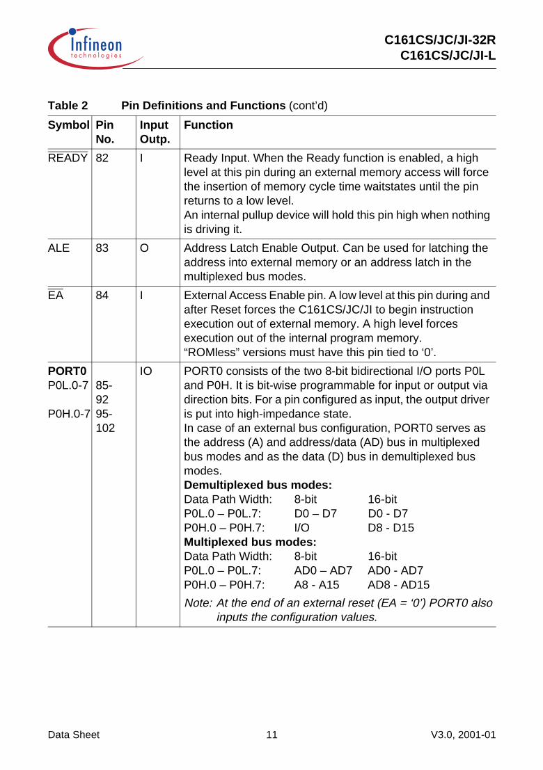
READY 82 I Ready Input. When the Ready function is enabled, a high level at this pin during an external memory access will force the insertion of memory cycle time waitstates until the pin returns to a low level.An internal pullup device will hold this pin high when nothing is driving it.
ALE 83 O Address Latch Enable Output. Can be used for latching the address into external memory or an address latch in the multiplexed bus modes.
EA 84 I External Access Enable pin. A low level at this pin during and after Reset forces the C161CS/JC/JI to begin instruction execution out of external memory. A high level forces execution out of the internal program memory.“ROMless” versions must have this pin tied to ‘0’.
PORT0P0L.0-7
P0H.0-7
85-9295-102
IO PORT0 consists of the two 8-bit bidirectional I/O ports P0L and P0H. It is bit-wise programmable for input or output via direction bits. For a pin configured as input, the output driver is put into high-impedance state.In case of an external bus configuration, PORT0 serves as the address (A) and address/data (AD) bus in multiplexed bus modes and as the data (D) bus in demultiplexed bus modes.Demultiplexed bus modes:Data Path Width: 8-bit 16-bitP0L.0 – P0L.7: D0 – D7 D0 - D7P0H.0 – P0H.7: I/O D8 - D15Multiplexed bus modes:Data Path Width: 8-bit 16-bitP0L.0 – P0L.7: AD0 – AD7 AD0 - AD7P0H.0 – P0H.7: A8 - A15 AD8 - AD15
Note: At the end of an external reset (EA = ‘0’) PORT0 alsoinputs the configuration values.
Table 2 Pin Definitions and Functions (cont’d)
Symbol PinNo.
InputOutp.
Function
Data Sheet 11 V3.0, 2001-01

C161CS/JC/JI-32RC161CS/JC/JI-L
PORT1P1L.0-7
P1H.0-7
P1H.4P1H.5P1H.6P1H.7
103-110113-120
117118119120
IO
I/OI/OI/OI/O
PORT1 consists of the two 8-bit bidirectional I/O ports P1L and P1H. It is bit-wise programmable for input or output via direction bits. For a pin configured as input, the output driver is put into high-impedance state. PORT1 is used as the 16-bit address bus (A) in demultiplexed bus modes and also after switching from a demultiplexed bus mode to a multiplexed bus mode.The following PORT1 pins also serve for alternate functions:CC24IO CAPCOM2: CC24 Capture Inp./Compare Outp.CC25IO CAPCOM2: CC25 Capture Inp./Compare Outp.CC26IO CAPCOM2: CC26 Capture Inp./Compare Outp.CC27IO CAPCOM2: CC27 Capture Inp./Compare Outp.
XTAL2XTAL1
123124
OI
XTAL2: Output of the oscillator amplifier circuit.XTAL1: Input to the oscillator amplifier and input to
the internal clock generatorTo clock the device from an external source, drive XTAL1, while leaving XTAL2 unconnected. Minimum and maximum high/low and rise/fall times specified in the AC Characteristics must be observed.
XTAL3
XTAL4
126
127
I
O
XTAL3: Input to the 32-kHz oscillator amplifier andinput to the internal clock generator
XTAL4: Output of the oscillator amplifier circuit.To clock the device from an external source, drive XTAL3, while leaving XTAL4 unconnected. Minimum and maximum high/low and rise/fall times specified in the AC Characteristics must be observed.
Table 2 Pin Definitions and Functions (cont’d)
Symbol PinNo.
InputOutp.
Function
Data Sheet 12 V3.0, 2001-01

C161CS/JC/JI-32RC161CS/JC/JI-L
RSTIN 128 I/O Reset Input with Schmitt-Trigger characteristics. A low level at this pin while the oscillator is running resets the C161CS/JC/JI. An internal pullup resistor permits power-on reset using only a capacitor connected to VSS.A spike filter suppresses input pulses < 10 ns. Input pulses > 100 ns safely pass the filter. The minimum duration for a safe recognition should be 100 ns + 2 CPU clock cycles.In bidirectional reset mode (enabled by setting bit BDRSTEN in register SYSCON) the RSTIN line is internally pulled low for the duration of the internal reset sequence upon any reset (HW, SW, WDT). See note below this table.
Note: To let the reset configuration of PORT0 settle and tolet the PLL lock a reset duration of ca. 1 ms isrecommended.
VAREF 35 – Reference voltage for the A/D converter.
VAGND 36 – Reference ground for the A/D converter.
VDD 4, 18,262), 42, 52, 68, 78, 93, 111, 121
– Digital Supply Voltage:+5 V during normal operation and idle mode.≥ 2.5 V during power down mode if RTC is off≥ 2.7 V during power down mode if RTC is running
VSS 3, 17,252), 41, 51, 69, 79, 94, 112, 122, 125
– Digital Ground.
1) The CAN and/or SDLM interface lines are assigned to ports P4 and P7 under software control. Within the CANmodule or SDLM several assignments can be selected.
2) Supply pins 25 and 26 feed the Analog/Digital Converter and should be decoupled separately.
Table 2 Pin Definitions and Functions (cont’d)
Symbol PinNo.
InputOutp.
Function
Data Sheet 13 V3.0, 2001-01

C161CS/JC/JI-32RC161CS/JC/JI-L
Note: The following behavioural differences must be observed when the bidirectionalreset is active:
• Bit BDRSTEN in register SYSCON cannot be changed after EINIT and is clearedautomatically after a reset.
• The reset indication flags always indicate a long hardware reset.• The PORT0 configuration is treated as if it were a hardware reset. In particular, the
bootstrap loader may be activated when P0L.4 is low.• Pin RSTIN may only be connected to external reset devices with an open drain output
driver.• A short hardware reset is extended to the duration of the internal reset sequence.
Data Sheet 14 V3.0, 2001-01

C161CS/JC/JI-32RC161CS/JC/JI-L
Functional Description
The architecture of the C161CS/JC/JI combines advantages of both RISC and CISCprocessors and of advanced peripheral subsystems in a very well-balanced way. Inaddition the on-chip memory blocks allow the design of compact systems with maximumperformance.The following block diagram gives an overview of the different on-chip components andof the advanced, high bandwidth internal bus structure of the C161CS/JC/JI.
Note: All time specifications refer to a CPU clock of 25 MHz(see definition in the AC Characteristics section).
Figure 3 Block Diagram
The program memory, the internal RAM (IRAM) and the set of generic peripherals areconnected to the CPU via separate buses. A fourth bus, the XBUS, connects externalresources as well as additional on-chip resoures, the X-Peripherals (see Figure 3).
The XBUS resources (XRAM, CAN, SDLM, IIC, ASC1) of the C161CS/JC/JI can beenabled during initialization by setting the general X-Peripheral enable bit XPEN(SYSCON.2).If the X-Peripherals remain disabled they consume neither address space nor port pins.
C166-Core
CPU
Por
t 2
Interrupt Bus
XTALOsc / PLL
RTC WDT
32
16
Interrupt Controller 16-LevelPriority
PECExternal Instr. / Data
GPTT2
T3
T4
T5
T6
SSC
BRGen
(SPI)ASC0
BRGen
(USART)ADC10-Bit
12Channels
CCOM1T0
T1
CCOM2T7
T8EBC
XBUS ControlExternal Bus
Control
IRAM
Dua
l Por
t
InternalRAM
2 KByte
ProgMem
ROM256 KByte
Data
Data
16
16
16
CAN/SDLM2.0B act. / Cl.B
Instr. / Data
Port 0
XRAM8 KByte
Por
t 6
8
8
Port 1
16 1216
Port 5 Port 3
15
Port 7
4
Port 9
6
Por
t 4
8
Peripheral Data Bus
ASC1(USART)
IIC400 KBd, 2 Ch.
16
On-
Chi
p X
BU
S (
16-B
it D
emux
)
MCB04323_1CSR
Data Sheet 15 V3.0, 2001-01

C161CS/JC/JI-32RC161CS/JC/JI-L
Memory Organization
The memory space of the C161CS/JC/JI is configured in a Von Neumann architecturewhich means that code memory, data memory, registers and I/O ports are organizedwithin the same linear address space which includes 16 MBytes. The entire memoryspace can be accessed bytewise or wordwise. Particular portions of the on-chip memoryhave additionally been made directly bitaddressable.
The C161CS/JC/JI incorporates 256 KBytes of on-chip mask-programmable ROM forcode or constant data. The lower 32 KBytes of the on-chip ROM can be mapped eitherto segment 0 or segment 1.
2 KBytes of on-chip Internal RAM (IRAM) are provided as a storage for user definedvariables, for the system stack, general purpose register banks and even for code. Aregister bank can consist of up to 16 wordwide (R0 to R15) and/or bytewide (RL0, RH0,…, RL7, RH7) so-called General Purpose Registers (GPRs).
1024 bytes (2 × 512 bytes) of the address space are reserved for the Special FunctionRegister areas (SFR space and ESFR space). SFRs are wordwide registers which areused for controlling and monitoring functions of the different on-chip units. Unused SFRaddresses are reserved for future members of the C166 Family.
8 KBytes of on-chip Extension RAM (XRAM) are provided to store user data, userstacks, or code. The XRAM is accessed like external memory and therefore cannot beused for the system stack or for register banks and is not bitaddressable. The XRAMpermits 16-bit accesses with maximum speed.
In order to meet the needs of designs where more memory is required than is providedon chip, up to 16 MBytes of external RAM and/or ROM can be connected to themicrocontroller.
Data Sheet 16 V3.0, 2001-01

C161CS/JC/JI-32RC161CS/JC/JI-L
External Bus Controller
All of the external memory accesses are performed by a particular on-chip External BusController (EBC). It can be programmed either to Single Chip Mode when no externalmemory is required, or to one of four different external memory access modes, whichare as follows:
– 16-/18-/20-/24-bit Addresses, 16-bit Data, Demultiplexed– 16-/18-/20-/24-bit Addresses, 16-bit Data, Multiplexed– 16-/18-/20-/24-bit Addresses, 8-bit Data, Multiplexed– 16-/18-/20-/24-bit Addresses, 8-bit Data, Demultiplexed
In the demultiplexed bus modes, addresses are output on PORT1 and data is input/output on PORT0 or P0L, respectively. In the multiplexed bus modes both addressesand data use PORT0 for input/output.
Important timing characteristics of the external bus interface (Memory Cycle Time,Memory Tri-State Time, Length of ALE and Read Write Delay) have been madeprogrammable to allow the user the adaption of a wide range of different types ofmemories and external peripherals.In addition, up to 4 independent address windows may be defined (via register pairsADDRSELx / BUSCONx) which control the access to different resources with differentbus characteristics. These address windows are arranged hierarchically whereBUSCON4 overrides BUSCON3 and BUSCON2 overrides BUSCON1. All accesses tolocations not covered by these 4 address windows are controlled by BUSCON0.
Up to 5 external CS signals (4 windows plus default) can be generated in order to saveexternal glue logic. The C161CS/JC/JI offers the possibility to switch the CS outputs toan unlatched mode. In this mode the internal filter logic is switched off and the CS signalsare directly generated from the address. The unlatched CS mode is enabled by settingCSCFG (SYSCON.6).
Access to very slow memories or memories with varying access times is supported viaa particular ‘Ready’ function.
A HOLD/HLDA protocol is available for bus arbitration and allows to share externalresources with other bus masters. The bus arbitration is enabled by setting bit HLDENin register PSW. After setting HLDEN once, pins P6.7 … P6.5 (BREQ, HLDA, HOLD)are automatically controlled by the EBC. In Master Mode (default after reset) the HLDApin is an output. By setting bit DP6.7 to ‘1’ the Slave Mode is selected where pin HLDAis switched to input. This allows to directly connect the slave controller to another mastercontroller without glue logic.
For applications which require less than 16 MBytes of external memory space, thisaddress space can be restricted to 1 MByte, 256 KByte, or to 64 KByte. In this casePort 4 outputs four, two, or no address lines at all. It outputs all 8 address lines, if anaddress space of 16 MBytes is used.
Data Sheet 17 V3.0, 2001-01

C161CS/JC/JI-32RC161CS/JC/JI-L
Note: When one or both of the on-chip CAN Modules or the SDLM are used with theinterface lines assigned to Port 4, the interface lines override the segment addresslines and the segment address output on Port 4 is therefore limited to 6/4 bits i.e.address lines A21/A19 … A16. CS lines can be used to increase the total amountof addressable external memory.
Central Processing Unit (CPU)
The main core of the CPU consists of a 4-stage instruction pipeline, a 16-bit arithmeticand logic unit (ALU) and dedicated SFRs. Additional hardware has been spent for aseparate multiply and divide unit, a bit-mask generator and a barrel shifter.
Based on these hardware provisions, most of the C161CS/JC/JI’s instructions can beexecuted in just one machine cycle which requires 80 ns at 25 MHz CPU clock. Forexample, shift and rotate instructions are always processed during one machine cycleindependent of the number of bits to be shifted. All multiple-cycle instructions have beenoptimized so that they can be executed very fast as well: branches in 2 cycles, a 16 × 16bit multiplication in 5 cycles and a 32-/16-bit division in 10 cycles. Another pipelineoptimization, the so-called ‘Jump Cache’, allows reducing the execution time ofrepeatedly performed jumps in a loop from 2 cycles to 1 cycle.
Figure 4 CPU Block Diagram
MCB02147
CPU
SPSTKOVSTKUN
Instr. Reg.Instr. Ptr.
Exec. Unit
4-StagePipeline
MDHMDL
PSWSYSCON Context Ptr.
Mul/Div-HW
R15
R0
General
Purpose
Registers
Bit-Mask Gen
Barrel - Shifter
ALU(16-bit)
Data Page Ptr. Code Seg. Ptr.
InternalRAM
R15
R0
ROM
16
16
32
BUSCON 0BUSCON 1BUSCON 2BUSCON 3BUSCON 4 ADDRSEL 4
ADDRSEL 3ADDRSEL 2ADDRSEL 1
Data Sheet 18 V3.0, 2001-01

C161CS/JC/JI-32RC161CS/JC/JI-L
The CPU has a register context consisting of up to 16 wordwide GPRs at its disposal.These 16 GPRs are physically allocated within the on-chip RAM area. A Context Pointer(CP) register determines the base address of the active register bank to be accessed bythe CPU at any time. The number of register banks is only restricted by the availableinternal RAM space. For easy parameter passing, a register bank may overlap others.
A system stack of up to 1024 words is provided as a storage for temporary data. Thesystem stack is allocated in the on-chip RAM area, and it is accessed by the CPU via thestack pointer (SP) register. Two separate SFRs, STKOV and STKUN, are implicitlycompared against the stack pointer value upon each stack access for the detection of astack overflow or underflow.
The high performance offered by the hardware implementation of the CPU can efficientlybe utilized by a programmer via the highly efficient C161CS/JC/JI instruction set whichincludes the following instruction classes:
– Arithmetic Instructions– Logical Instructions– Boolean Bit Manipulation Instructions– Compare and Loop Control Instructions– Shift and Rotate Instructions– Prioritize Instruction– Data Movement Instructions– System Stack Instructions– Jump and Call Instructions– Return Instructions– System Control Instructions– Miscellaneous Instructions
The basic instruction length is either 2 or 4 bytes. Possible operand types are bits, bytesand words. A variety of direct, indirect or immediate addressing modes are provided tospecify the required operands.
Data Sheet 19 V3.0, 2001-01
C161CS/JC/JI-32RC161CS/JC/JI-L
Interrupt System
With an interrupt response time within a range from just 5 to 12 CPU clocks (in case ofinternal program execution), the C161CS/JC/JI is capable of reacting very fast to theoccurrence of non-deterministic events.
The architecture of the C161CS/JC/JI supports several mechanisms for fast and flexibleresponse to service requests that can be generated from various sources internal orexternal to the microcontroller. Any of these interrupt requests can be programmed tobeing serviced by the Interrupt Controller or by the Peripheral Event Controller (PEC).
In contrast to a standard interrupt service where the current program execution issuspended and a branch to the interrupt vector table is performed, just one cycle is‘stolen’ from the current CPU activity to perform a PEC service. A PEC service impliesa single byte or word data transfer between any two memory locations with an additionalincrement of either the PEC source or the destination pointer. An individual PEC transfercounter is implicity decremented for each PEC service except when performing in thecontinuous transfer mode. When this counter reaches zero, a standard interrupt isperformed to the corresponding source related vector location. PEC services are verywell suited, for example, for supporting the transmission or reception of blocks of data.The C161CS/JC/JI has 8 PEC channels each of which offers such fast interrupt-drivendata transfer capabilities.
A separate control register which contains an interrupt request flag, an interrupt enableflag and an interrupt priority bitfield exists for each of the possible interrupt sources. Viaits related register, each source can be programmed to one of sixteen interrupt prioritylevels. Once having been accepted by the CPU, an interrupt service can only beinterrupted by a higher prioritized service request. For the standard interrupt processing,each of the possible interrupt sources has a dedicated vector location.
Fast external interrupt inputs are provided to service external interrupts with highprecision requirements. These fast interrupt inputs feature programmable edgedetection (rising edge, falling edge or both edges).
Software interrupts are supported by means of the ‘TRAP’ instruction in combination withan individual trap (interrupt) number.
Table 3 shows all of the possible C161CS/JC/JI interrupt sources and the correspondinghardware-related interrupt flags, vectors, vector locations and trap (interrupt) numbers.
Note: Interrupt nodes which are not used by associated peripherals, may be used togenerate software controlled interrupt requests by setting the respective interruptrequest bit (xIR).
Data Sheet 20 V3.0, 2001-01

C161CS/JC/JI-32RC161CS/JC/JI-L
Table 3 C161CS/JC/JI Interrupt Nodes
Source of Interrupt or PEC Service Request
RequestFlag
EnableFlag
InterruptVector
VectorLocation
TrapNumber
CAPCOM Register 0 CC0IR CC0IE CC0INT 00’0040H 10H
CAPCOM Register 1 CC1IR CC1IE CC1INT 00’0044H 11H
CAPCOM Register 2 CC2IR CC2IE CC2INT 00’0048H 12H
CAPCOM Register 3 CC3IR CC3IE CC3INT 00’004CH 13H
CAPCOM Register 4 CC4IR CC4IE CC4INT 00’0050H 14H
CAPCOM Register 5 CC5IR CC5IE CC5INT 00’0054H 15H
CAPCOM Register 6 CC6IR CC6IE CC6INT 00’0058H 16H
CAPCOM Register 7 CC7IR CC7IE CC7INT 00’005CH 17H
CAPCOM Register 8 CC8IR CC8IE CC8INT 00’0060H 18H
CAPCOM Register 9 CC9IR CC9IE CC9INT 00’0064H 19H
CAPCOM Register 10 CC10IR CC10IE CC10INT 00’0068H 1AH
CAPCOM Register 11 CC11IR CC11IE CC11INT 00’006CH 1BH
CAPCOM Register 12 CC12IR CC12IE CC12INT 00’0070H 1CH
CAPCOM Register 13 CC13IR CC13IE CC13INT 00’0074H 1DH
CAPCOM Register 14 CC14IR CC14IE CC14INT 00’0078H 1EH
CAPCOM Register 15 CC15IR CC15IE CC15INT 00’007CH 1FH
CAPCOM Register 16 CC16IR CC16IE CC16INT 00’00C0H 30H
CAPCOM Register 17 CC17IR CC17IE CC17INT 00’00C4H 31H
CAPCOM Register 18 CC18IR CC18IE CC18INT 00’00C8H 32H
CAPCOM Register 19 CC19IR CC19IE CC19INT 00’00CCH 33H
CAPCOM Register 20 CC20IR CC20IE CC20INT 00’00D0H 34H
CAPCOM Register 21 CC21IR CC21IE CC21INT 00’00D4H 35H
CAPCOM Register 22 CC22IR CC22IE CC22INT 00’00D8H 36H
CAPCOM Register 23 CC23IR CC23IE CC23INT 00’00DCH 37H
CAPCOM Register 24 CC24IR CC24IE CC24INT 00’00E0H 38H
CAPCOM Register 25 CC25IR CC25IE CC25INT 00’00E4H 39H
CAPCOM Register 26 CC26IR CC26IE CC26INT 00’00E8H 3AH
CAPCOM Register 27 CC27IR CC27IE CC27INT 00’00ECH 3BH
CAPCOM Register 28 CC28IR CC28IE CC28INT 00’00E0H 3CH
CAPCOM Register 29 CC29IR CC29IE CC29INT 00’0110H 44H
Data Sheet 21 V3.0, 2001-01

C161CS/JC/JI-32RC161CS/JC/JI-L
CAPCOM Register 30 CC30IR CC30IE CC30INT 00’0114H 45H
CAPCOM Register 31 CC31IR CC31IE CC31INT 00’0118H 46H
CAPCOM Timer 0 T0IR T0IE T0INT 00’0080H 20H
CAPCOM Timer 1 T1IR T1IE T1INT 00’0084H 21H
CAPCOM Timer 7 T7IR T7IE T7INT 00’00F4H 3DH
CAPCOM Timer 8 T8IR T8IE T8INT 00’00F8H 3EH
GPT1 Timer 2 T2IR T2IE T2INT 00’0088H 22H
GPT1 Timer 3 T3IR T3IE T3INT 00’008CH 23H
GPT1 Timer 4 T4IR T4IE T4INT 00’0090H 24H
GPT2 Timer 5 T5IR T5IE T5INT 00’0094H 25H
GPT2 Timer 6 T6IR T6IE T6INT 00’0098H 26H
GPT2 CAPREL Reg. CRIR CRIE CRINT 00’009CH 27H
A/D Conversion Compl. ADCIR ADCIE ADCINT 00’00A0H 28H
A/D Overrun Error ADEIR ADEIE ADEINT 00’00A4H 29H
ASC0 Transmit S0TIR S0TIE S0TINT 00’00A8H 2AH
ASC0 Transmit Buffer S0TBIR S0TBIE S0TBINT 00’011CH 47H
ASC0 Receive S0RIR S0RIE S0RINT 00’00ACH 2BH
ASC0 Error S0EIR S0EIE S0EINT 00’00B0H 2CH
SSC Transmit SCTIR SCTIE SCTINT 00’00B4H 2DH
SSC Receive SCRIR SCRIE SCRINT 00’00B8H 2EH
SSC Error SCEIR SCEIE SCEINT 00’00BCH 2FH
IIC Data Transfer Event XP0IR XP0IE XP0INT 00’0100H 40H
IIC Protocol Event XP1IR XP1IE XP1INT 00’0104H 41H
CAN1 (C161CS/JC) XP2IR XP2IE XP2INT 00’0108H 42H
PLL/OWD and RTC XP3IR XP3IE XP3INT 00’010CH 43H
ASC1 Transmit XP4IR XP4IE XP4INT 00’0120H 48H
ASC1 Receive XP5IR XP5IE XP5INT 00’0124H 49H
ASC1 Error XP6IR XP6IE XP6INT 00’0128H 4AH
CAN2 (C161CS) orSDLM (C161JC/JI)
XP7IR XP7IE XP7INT 00’012CH 4BH
Table 3 C161CS/JC/JI Interrupt Nodes (cont’d)
Source of Interrupt or PEC Service Request
RequestFlag
EnableFlag
InterruptVector
VectorLocation
TrapNumber
Data Sheet 22 V3.0, 2001-01
C161CS/JC/JI-32RC161CS/JC/JI-L
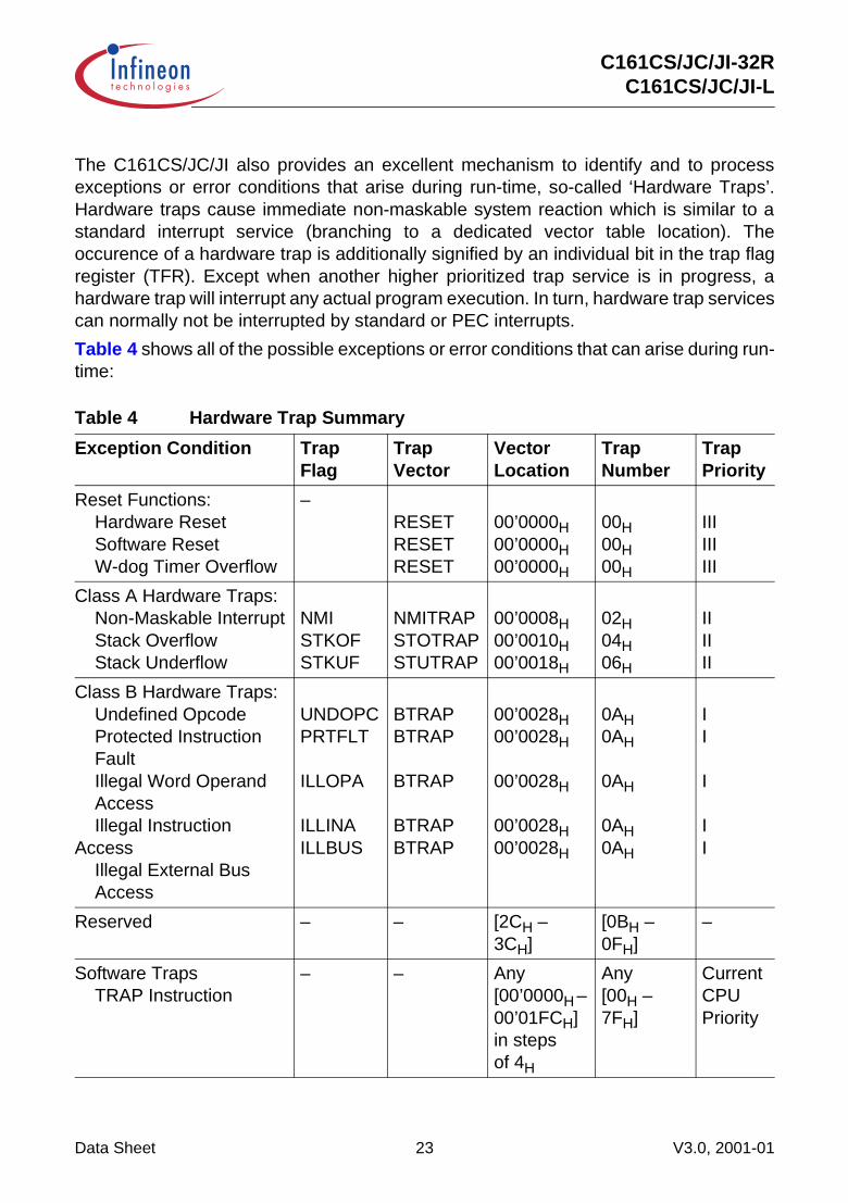
The C161CS/JC/JI also provides an excellent mechanism to identify and to processexceptions or error conditions that arise during run-time, so-called ‘Hardware Traps’.Hardware traps cause immediate non-maskable system reaction which is similar to astandard interrupt service (branching to a dedicated vector table location). Theoccurence of a hardware trap is additionally signified by an individual bit in the trap flagregister (TFR). Except when another higher prioritized trap service is in progress, ahardware trap will interrupt any actual program execution. In turn, hardware trap servicescan normally not be interrupted by standard or PEC interrupts.
Table 4 shows all of the possible exceptions or error conditions that can arise during run-time:
Table 4 Hardware Trap Summary
Exception Condition TrapFlag
TrapVector
VectorLocation
TrapNumber
TrapPriority
Reset Functions:Hardware ResetSoftware ResetW-dog Timer Overflow
–RESETRESETRESET
00’0000H00’0000H00’0000H
00H00H00H
IIIIIIIII
Class A Hardware Traps:Non-Maskable InterruptStack OverflowStack Underflow
NMISTKOFSTKUF
NMITRAPSTOTRAPSTUTRAP
00’0008H00’0010H00’0018H
02H04H06H
IIIIII
Class B Hardware Traps:Undefined OpcodeProtected InstructionFaultIllegal Word OperandAccessIllegal Instruction
AccessIllegal External BusAccess
UNDOPCPRTFLT
ILLOPA
ILLINAILLBUS
BTRAPBTRAP
BTRAP
BTRAPBTRAP
00’0028H00’0028H
00’0028H
00’0028H00’0028H
0AH0AH
0AH
0AH0AH
II
I
II
Reserved – – [2CH – 3CH]
[0BH – 0FH]
–
Software TrapsTRAP Instruction
– – Any[00’0000H – 00’01FCH]in stepsof 4H
Any[00H – 7FH]
CurrentCPU Priority
Data Sheet 23 V3.0, 2001-01

C161CS/JC/JI-32RC161CS/JC/JI-L
Capture/Compare (CAPCOM) Units
The CAPCOM units support generation and control of timing sequences on up to32 channels with a maximum resolution of 16 TCL. The CAPCOM units are typicallyused to handle high speed I/O tasks such as pulse and waveform generation, pulsewidth modulation (PMW), Digital to Analog (D/A) conversion, software timing, or timerecording relative to external events.
Four 16-bit timers (T0/T1, T7/T8) with reload registers provide two independent timebases for the capture/compare register array.
The input clock for the timers is programmable to several prescaled values of the internalsystem clock, or may be derived from an overflow/underflow of timer T6 in moduleGPT2. This provides a wide range of variation for the timer period and resolution andallows precise adjustments to the application specific requirements. In addition, externalcount inputs for CAPCOM timers T0 and T7 allow event scheduling for the capture/compare registers relative to external events.
Both of the two capture/compare register arrays contain 16 dual purpose capture/compare registers, each of which may be individually allocated to either CAPCOM timerT0 or T1 (T7 or T8, respectively), and programmed for capture or compare function.Eight registers of each module have one port pin associated with it which serves as aninput pin for triggering the capture function, or as an output pin to indicate the occurrenceof a compare event.
When a capture/compare register has been selected for capture mode, the currentcontents of the allocated timer will be latched (‘captured’) into the capture/compareregister in response to an external event at the port pin which is associated with thisregister. In addition, a specific interrupt request for this capture/compare register isgenerated. Either a positive, a negative, or both a positive and a negative external signaltransition at the pin can be selected as the triggering event.
The contents of all registers which have been selected for one of the five comparemodes are continuously compared with the contents of the allocated timers.
Table 5 Compare Modes (CAPCOM)
Compare Modes Function
Mode 0 Interrupt-only compare mode;several compare interrupts per timer period are possible
Mode 1 Pin toggles on each compare match;several compare events per timer period are possible
Mode 2 Interrupt-only compare mode;only one compare interrupt per timer period is generated
Mode 3 Pin set ‘1’ on match; pin reset ‘0’ on compare time overflow;only one compare event per timer period is generated
Data Sheet 24 V3.0, 2001-01

C161CS/JC/JI-32RC161CS/JC/JI-L
When a match occurs between the timer value and the value in a capture/compareregister, specific actions will be taken based on the selected compare mode.
Figure 5 CAPCOM Unit Block Diagram
MCB02143c
ModeControl
(Captureor
Compare)
2n : 1fCPU
TxInput
ControlCAPCOM Timer Tx
TyInput
Control
TxIN
InterruptRequest
GPT2 Timer T6Over/Underflow
2n : 1fCPU
GPT2 Timer T6Over/Underflow
CCxIO
CCxIO
8 Capture Inputs8 Compare Outputs
Reload Reg. TxREL
CAPCOM Timer Ty
Reload Reg. TyREL
InterruptRequest
16 Capture/CompareInterrupt Request
16-BitCapture/CompareRegisters
x = 0, 7y = 1, 8n = 3 … 10
Data Sheet 25 V3.0, 2001-01

C161CS/JC/JI-32RC161CS/JC/JI-L
General Purpose Timer (GPT) Unit
The GPT unit represents a very flexible multifunctional timer/counter structure whichmay be used for many different time related tasks such as event timing and counting,pulse width and duty cycle measurements, pulse generation, or pulse multiplication.
The GPT unit incorporates five 16-bit timers which are organized in two separatemodules, GPT1 and GPT2. Each timer in each module may operate independently in anumber of different modes, or may be concatenated with another timer of the samemodule.
Each of the three timers T2, T3, T4 of module GPT1 can be configured individually forone of four basic modes of operation, which are Timer, Gated Timer, Counter, andIncremental Interface Mode. In Timer Mode, the input clock for a timer is derived fromthe CPU clock, divided by a programmable prescaler, while Counter Mode allows a timerto be clocked in reference to external events.Pulse width or duty cycle measurement is supported in Gated Timer Mode, where theoperation of a timer is controlled by the ‘gate’ level on an external input pin. For thesepurposes, each timer has one associated port pin (TxIN) which serves as gate or clockinput. The maximum resolution of the timers in module GPT1 is 16 TCL.
The count direction (up/down) for each timer is programmable by software or mayadditionally be altered dynamically by an external signal on a port pin (TxEUD) tofacilitate e.g. position tracking.
In Incremental Interface Mode the GPT1 timers (T2, T3, T4) can be directly connectedto the incremental position sensor signals A and B via their respective inputs TxIN andTxEUD. Direction and count signals are internally derived from these two input signals,so the contents of the respective timer Tx corresponds to the sensor position. The thirdposition sensor signal TOP0 can be connected to an interrupt input.
Timer T3 has an output toggle latch (T3OTL) which changes its state on each timer over-flow/underflow. The state of this latch may be output on pin T3OUT e.g. for time outmonitoring of external hardware components, or may be used internally to clock timersT2 and T4 for measuring long time periods with high resolution.
In addition to their basic operating modes, timers T2 and T4 may be configured as reloador capture registers for timer T3. When used as capture or reload registers, timers T2and T4 are stopped. The contents of timer T3 is captured into T2 or T4 in response to asignal at their associated input pins (TxIN). Timer T3 is reloaded with the contents of T2or T4 triggered either by an external signal or by a selectable state transition of its togglelatch T3OTL. When both T2 and T4 are configured to alternately reload T3 on oppositestate transitions of T3OTL with the low and high times of a PWM signal, this signal canbe constantly generated without software intervention.
Data Sheet 26 V3.0, 2001-01

C161CS/JC/JI-32RC161CS/JC/JI-L
Figure 6 Block Diagram of GPT1
With its maximum resolution of 8 TCL, the GPT2 module provides precise event controland time measurement. It includes two timers (T5, T6) and a capture/reload register(CAPREL). Both timers can be clocked with an input clock which is derived from the CPUclock via a programmable prescaler or with external signals. The count direction (up/down) for each timer is programmable by software or may additionally be altereddynamically by an external signal on a port pin (TxEUD). Concatenation of the timers issupported via the output toggle latch (T6OTL) of timer T6, which changes its state oneach timer overflow/underflow.
The state of this latch may be used to clock timer T5, and/or it may be output on pinT6OUT. The overflows/underflows of timer T6 can additionally be used to clock theCAPCOM timers T0 or T1, and to cause a reload from the CAPREL register. TheCAPREL register may capture the contents of timer T5 based on an external signaltransition on the corresponding port pin (CAPIN), and timer T5 may optionally be cleared
T3Mode
Control
2n : 1fCPU
2n : 1fCPU T2Mode
Control
GPT1 Timer T2
Reload
Capture
2n : 1fCPU
T4Mode
Control GPT1 Timer T4
Reload
Capture
GPT1 Timer T3 T3OTL
U/D
T2EUD
T2IN
T3IN
T3EUD
T4IN
T4EUD
T3OUT
Toggle FF
U/D
U/D
InterruptRequest(T2IR)
InterruptRequest(T3IR)
InterruptRequest(T4IR)
MCT04825
n = 3 … 10
Data Sheet 27 V3.0, 2001-01

C161CS/JC/JI-32RC161CS/JC/JI-L
after the capture procedure. This allows the C161CS/JC/JI to measure absolute timedifferences or to perform pulse multiplication without software overhead.
The capture trigger (timer T5 to CAPREL) may also be generated upon transitions ofGPT1 timer T3’s inputs T3IN and/or T3EUD. This is especially advantageous when T3operates in Incremental Interface Mode.
Figure 7 Block Diagram of GPT2
n = 2 … 9
MUX
2n : 1fCPU T5Mode
Control
GPT2 Timer T5
2n : 1fCPU
T6Mode
Control
GPT2 Timer T6
GPT2 CAPREL
T6OTL
T5IN
T3
CAPIN
T6IN T6OUT
U/D
U/D
InterruptRequest(T5IR)
InterruptRequest(CRIR)
InterruptRequest(T6IR)
To auxiliaryTimers
Clear
Capture
CT3
mcb03999b.vsd
To otherModules
Data Sheet 28 V3.0, 2001-01

C161CS/JC/JI-32RC161CS/JC/JI-L
Real Time Clock
The Real Time Clock (RTC) module of the C161CS/JC/JI consists of a chain of 3 dividerblocks, a fixed 8:1 divider, the reloadable 16-bit timer T14, and the 32-bit RTC timer(accessible via registers RTCH and RTCL). The RTC module is directly clocked via aseparate clock driver with the on-chip main oscillator frequency divided by 32(fRTC = fOSCm / 32) or with the on-chip auxiliary oscillator frequency (fRTC = fOSCa). It istherefore independent from the selected clock generation mode of the C161CS/JC/JI.All timers count up.
The RTC module can be used for different purposes:
• System clock to determine the current time and date• Cyclic time based interrupt• 48-bit timer for long term measurements
Figure 8 RTC Block Diagram
Note: The registers associated with the RTC are not affected by a reset in order tomaintain the correct system time even when intermediate resets are executed.
MCD04432
T14REL
T14 8:1RTCf
RTCLRTCH
InterruptRequest
Reload
Data Sheet 29 V3.0, 2001-01

C161CS/JC/JI-32RC161CS/JC/JI-L
A/D Converter
For analog signal measurement, a 10-bit A/D converter with 12 multiplexed inputchannels and a sample and hold circuit has been integrated on-chip. It uses the methodof successive approximation. The sample time (for loading the capacitors) and theconversion time is programmable and can so be adjusted to the external circuitry.
Overrun error detection/protection is provided for the conversion result register(ADDAT): either an interrupt request will be generated when the result of a previousconversion has not been read from the result register at the time the next conversion iscomplete, or the next conversion is suspended in such a case until the previous resulthas been read.
For applications which require less than 12 analog input channels, the remainingchannel inputs can be used as digital input port pins.
The A/D converter of the C161CS/JC/JI supports four different conversion modes. In thestandard Single Channel conversion mode, the analog level on a specified channel issampled once and converted to a digital result. In the Single Channel Continuous mode,the analog level on a specified channel is repeatedly sampled and converted withoutsoftware intervention. In the Auto Scan mode, the analog levels on a prespecifiednumber of channels (standard or extension) are sequentially sampled and converted. Inthe Auto Scan Continuous mode, the number of prespecified channels is repeatedlysampled and converted. In addition, the conversion of a specific channel can be inserted(injected) into a running sequence without disturbing this sequence. This is calledChannel Injection Mode.
The Peripheral Event Controller (PEC) may be used to automatically store theconversion results into a table in memory for later evaluation, without requiring theoverhead of entering and exiting interrupt routines for each data transfer.
After each reset and also during normal operation the ADC automatically performscalibration cycles. This automatic self-calibration constantly adjusts the converter tochanging operating conditions (e.g. temperature) and compensates process variations.
These calibration cycles are part of the conversion cycle, so they do not affect the normaloperation of the A/D converter.
In order to decouple analog inputs from digital noise and to avoid input trigger noisethose pins used for analog input can be disconnected from the digital IO or input stagesunder software control. This can be selected for each pin separately via registerP5DIDIS (Port 5 Digital Input Disable).
Data Sheet 30 V3.0, 2001-01

C161CS/JC/JI-32RC161CS/JC/JI-L
Serial Channels
Serial communication with other microcontrollers, processors, terminals or externalperipheral components is provided by three serial interfaces with different functionality,two Asynchronous/Synchronous Serial Channels (ASC0/ASC1) and a High-SpeedSynchronous Serial Channel (SSC).
The ASC0 is upward compatible with the serial ports of the Infineon 8-bit microcontrollerfamilies and supports full-duplex asynchronous communication at up to 781 kBaud andhalf-duplex synchronous communication at up to 3.1 MBaud (@ 25 MHz CPU clock).A dedicated baud rate generator allows to set up all standard baud rates withoutoscillator tuning. For transmission, reception and error handling 4 separate interruptvectors are provided. In asynchronous mode, 8- or 9-bit data frames are transmitted orreceived, preceded by a start bit and terminated by one or two stop bits. Formultiprocessor communication, a mechanism to distinguish address from data bytes hasbeen included (8-bit data plus wake up bit mode).In synchronous mode, the ASC0 transmits or receives bytes (8 bits) synchronously to ashift clock which is generated by the ASC0. The ASC0 always shifts the LSB first. A loopback option is available for testing purposes.A number of optional hardware error detection capabilities has been included to increasethe reliability of data transfers. A parity bit can automatically be generated ontransmission or be checked on reception. Framing error detection allows to recognizedata frames with missing stop bits. An overrun error will be generated, if the lastcharacter received has not been read out of the receive buffer register at the time thereception of a new character is complete.
The ASC1 is function compatible with the ASC0, except that its registers are not bit-addressable (XBUS peripheral) and it provides only three interrupt vectors.
The SSC supports full-duplex synchronous communication at up to 6.25 MBaud(@ 25 MHz CPU clock). It may be configured so it interfaces with serially linkedperipheral components. A dedicated baud rate generator allows to set up all standardbaud rates without oscillator tuning. For transmission, reception and error handling threeseparate interrupt vectors are provided.The SSC transmits or receives characters of 2 … 16 bits length synchronously to a shiftclock which can be generated by the SSC (master mode) or by an external master (slavemode). The SSC can start shifting with the LSB or with the MSB and allows the selectionof shifting and latching clock edges as well as the clock polarity.A number of optional hardware error detection capabilities has been included to increasethe reliability of data transfers. Transmit and receive error supervise the correct handlingof the data buffer. Phase and baudrate error detect incorrect serial data.
Data Sheet 31 V3.0, 2001-01

C161CS/JC/JI-32RC161CS/JC/JI-L
Serial Data Link Module (SDLM)
The Serial Data Link Module (SDLM) provides serial communication via a J1850 typemultiplexed serial bus via an external J1850 bus transceiver. The module conforms tothe SAE Class B J1850 specification for variable pulse width modulation (VPW). TheSDLM is integrated as an on-chip peripheral and is connected to the CPU via the XBUS.
General SDLM Features:
• Compliant to the SAE Class B J1850 specification (VPW)• Class 2 protocol fully supported• Variable Pulse Width (VPW) operation at 10.4 kBaud• High Speed 4X operation at 41.6 kBaud• Programmable Normalization Bit• Programmable Delay for transceiver interface• Digital Noise Filter• Power Down mode with automatic wakeup support upon bus activity• Single Byte Header and Consolidated Header supported• CRC generation and checking• Receive and transmit Block Mode
Data Link Operation Features:
• 11 Byte Transmit Buffer• Double buffered 11 Byte receive buffer (optional overwrite enable)• Support for In Frame Response (IFR) types 1, 2 and 3• Transmit and Receiver Message Buffers configurable for either FIFO or Byte mode• Advanced Interrupt Handling with 8 separately enabled sources:
Error, format or bus shortedCRC errorLost ArbitrationBreak receivedIn-Frame-Response requestHeader receivedComplete message receivedTransmit successful
• Automatic IFR transmission (Types 1 and 2) for 3-Byte consolidated headers• User configurable clock divider• Bus status flags (IDLE, EOF, EOD, SOF, Tx and Rx in progress)
Note: When the SDLM is used with the interface lines assigned to Port 4, the interfacelines override the segment address lines and the segment address output onPort 4 is therefore limited to 6/4 bits i.e. address lines A21/A19 … A16. CS linescan be used to increase the total amount of addressable external memory.
Data Sheet 32 V3.0, 2001-01

C161CS/JC/JI-32RC161CS/JC/JI-L
CAN-Modules
The integrated CAN-Modules handle the completely autonomous transmission andreception of CAN frames in accordance with the CAN specification V2.0 part B (active),i.e. the on-chip CAN-Modules can receive and transmit standard frames with 11-bitidentifiers as well as extended frames with 29-bit identifiers.
The modules provide Full CAN functionality on up to 15 message objects each.Message object 15 may be configured for Basic CAN functionality. Both modes provideseparate masks for acceptance filtering which allows to accept a number of identifiers inFull CAN mode and also allows to disregard a number of identifiers in Basic CAN mode.All message objects can be updated independent from the other objects and areequipped for the maximum message length of 8 bytes.
The bit timing is derived from the XCLK and is programmable up to a data rate of1 MBaud. Each CAN-Module uses two pins of Port 4 or Port 8 to interface to an externalbus transceiver. The interface pins are assigned via software.
Module CAN2 (C161CS only) is identical with the first one, except that it uses a separateaddress area and a separate interrupt node.
The two CAN modules can be internally coupled by assigning their interface pins to thesame two port pins, or they can interface to separate CAN buses.
Note: When one or both of the on-chip CAN Modules are used with the interface linesassigned to Port 4, the interface lines override the segment address lines and thesegment address output on Port 4 is therefore limited to 6/4 bits i.e. address linesA21/A19 … A16. CS lines can be used to increase the total amount of addressableexternal memory.
IIC Module
The integrated IIC Bus Module handles the transmission and reception of frames overthe two-line IIC bus in accordance with the IIC Bus specification. The on-chip IIC Modulecan receive and transmit data using 7-bit or 10-bit addressing and it can operate in slavemode, in master mode or in multi-master mode.
Several physical interfaces (port pins) can be established under software control. Datacan be transferred at speeds up to 400 kbit/sec.
Two interrupt nodes dedicated to the IIC module allow efficient interrupt service and alsosupport operation via PEC transfers.
Note: The port pins associated with the IIC interfaces feature open drain drivers only, asrequired by the IIC specification.
Data Sheet 33 V3.0, 2001-01

C161CS/JC/JI-32RC161CS/JC/JI-L
Parallel Ports
The C161CS/JC/JI provides up to 93 I/O lines which are organized into eight input/outputports and one input port. All port lines are bit-addressable, and all input/output lines areindividually (bit-wise) programmable as inputs or outputs via direction registers. The I/Oports are true bidirectional ports which are switched to high impedance state whenconfigured as inputs. The output drivers of five I/O ports can be configured (pin by pin)for push/pull operation or open-drain operation via control registers, Port 9 providesopen-drain-only drivers. During the internal reset, all port pins are configured as inputs.
The input threshold of Port 2, Port 3, Port 4, Port 6, and Port 7 is selectable (TTL orCMOS like), where the special CMOS like input threshold reduces noise sensitivity dueto the input hysteresis. The input threshold may be selected individually for each byte ofthe respective ports.
All port lines have programmable alternate input or output functions associated withthem. All port lines that are not used for these alternate functions may be used asgeneral purpose IO lines.
PORT0 and PORT1 may be used as address and data lines when accessing externalmemory, while Port 4 outputs the additional segment address bits A23/19/17 … A16 insystems where segmentation is enabled to access more than 64 KBytes of memory.Port 2, Port 7, and parts of PORT1 are associated with the capture inputs or compareoutputs of the CAPCOM units.Port 6 provides optional bus arbitration signals (BREQ, HLDA, HOLD) and chip selectsignals.Port 3 includes alternate functions of timers, serial interfaces, the optional bus controlsignal BHE, and the system clock output CLKOUT (or the programmable frequencyoutput FOUT).Port 5 is used for the analog input channels to the A/D converter or timer control signals.
The edge characteristics (transition time) and driver characteristics (output current) ofthe C161CS/JC/JI’s port drivers can be selected via the Port Output Control registers(POCONx).
Data Sheet 34 V3.0, 2001-01

C161CS/JC/JI-32RC161CS/JC/JI-L
Watchdog Timer
The Watchdog Timer represents one of the fail-safe mechanisms which have beenimplemented to prevent the controller from malfunctioning for longer periods of time.
The Watchdog Timer is always enabled after a reset of the chip, and can only bedisabled in the time interval until the EINIT (end of initialization) instruction has beenexecuted. Thus, the chip’s start-up procedure is always monitored. The software has tobe designed to service the Watchdog Timer before it overflows. If, due to hardware orsoftware related failures, the software fails to do so, the Watchdog Timer overflows andgenerates an internal hardware reset and pulls the RSTOUT pin low in order to allowexternal hardware components to be reset.
The Watchdog Timer is a 16-bit timer, clocked with the system clock divided by 2/4/128/256. The high byte of the Watchdog Timer register can be set to a prespecified reloadvalue (stored in WDTREL) in order to allow further variation of the monitored timeinterval. Each time it is serviced by the application software, the high byte of theWatchdog Timer is reloaded. Thus, time intervals between 20 µs and 671 ms can bemonitored (@ 25 MHz).The default Watchdog Timer interval after reset is 5.24 ms (@ 25 MHz).
Oscillator Watchdog
The Oscillator Watchdog (OWD) monitors the clock signal generated by the on-chiposcillator (either with a crystal or via external clock drive). For this operation the PLLprovides a clock signal which is used to supervise transitions on the oscillator clock. ThisPLL clock is independent from the XTAL1 clock. When the expected oscillator clocktransitions are missing the OWD activates the PLL Unlock / OWD interrupt node andsupplies the CPU with the PLL clock signal. Under these circumstances the PLL willoscillate with its basic frequency.
In direct drive mode the PLL base frequency is used directly (fCPU = 2 … 5 MHz).In prescaler mode the PLL base frequency is divided by 2 (fCPU = 1 … 2.5 MHz).
Note: The CPU clock source is only switched back to the oscillator clock after ahardware reset.
The oscillator watchdog can be disabled by setting bit OWDDIS in register SYSCON.In this case (OWDDIS = ‘1’) the PLL remains idle and provides no clock signal, while theCPU clock signal is derived directly from the oscillator clock or via prescaler or SDD. Alsono interrupt request will be generated in case of a missing oscillator clock.
Note: At the end of an external reset (EA = ‘0’) bit OWDDIS reflects the inverted level ofpin RD at that time. Thus the oscillator watchdog may also be disabled viahardware by (externally) pulling the RD line low upon a reset, similar to thestandard reset configuration via PORT0. At the end of an internal reset (EA = ‘1’)bit OWDDIS is cleared.
Data Sheet 35 V3.0, 2001-01

C161CS/JC/JI-32RC161CS/JC/JI-L
Power Management
The C161CS/JC/JI provides several means to control the power it consumes either at agiven time or averaged over a certain timespan. Three mechanisms can be used (partlyin parallel):
• Power Saving Modes switch the C161CS/JC/JI into a special operating mode(control via instructions).Idle Mode stops the CPU while the peripherals can continue to operate.Sleep Mode and Power Down Mode stop all clock signals and all operation (RTC mayoptionally continue running). Sleep Mode can be terminated by external interruptsignals.
• Clock Generation Management controls the distribution and the frequency ofinternal and external clock signals (control via register SYSCON2).Slow Down Mode lets the C161CS/JC/JI run at a CPU clock frequency of fOSC /1 … 32 (half for prescaler operation) which drastically reduces the consumed power.The PLL can be optionally disabled while operating in Slow Down Mode.External circuitry can be controlled via the programmable frequency output FOUT.
• Peripheral Management permits temporary disabling of peripheral modules (controlvia register SYSCON3).Each peripheral can separately be disabled/enabled. A group control option disablesa major part of the peripheral set by setting one single bit.
The on-chip RTC supports intermittend operation of the C161CS/JC/JI by generatingcyclic wakeup signals. This offers full performance to quickly react on action requestswhile the intermittend sleep phases greatly reduce the average power consumption ofthe system.
Data Sheet 36 V3.0, 2001-01

C161CS/JC/JI-32RC161CS/JC/JI-L
Instruction Set Summary
Table 6 lists the instructions of the C161CS/JC/JI in a condensed way.The various addressing modes that can be used with a specific instruction, the operationof the instructions, parameters for conditional execution of instructions, and the opcodesfor each instruction can be found in the “C166 Family Instruction Set Manual” .
This document also provides a detailled description of each instruction.
Table 6 Instruction Set Summary
Mnemonic Description BytesADD(B) Add word (byte) operands 2 / 4ADDC(B) Add word (byte) operands with Carry 2 / 4
SUB(B) Subtract word (byte) operands 2 / 4
SUBC(B) Subtract word (byte) operands with Carry 2 / 4MUL(U) (Un)Signed multiply direct GPR by direct GPR (16-16-bit) 2
DIV(U) (Un)Signed divide register MDL by direct GPR (16-/16-bit) 2
DIVL(U) (Un)Signed long divide reg. MD by direct GPR (32-/16-bit) 2CPL(B) Complement direct word (byte) GPR 2
NEG(B) Negate direct word (byte) GPR 2
AND(B) Bitwise AND, (word/byte operands) 2 / 4OR(B) Bitwise OR, (word/byte operands) 2 / 4
XOR(B) Bitwise XOR, (word/byte operands) 2 / 4
BCLR Clear direct bit 2BSET Set direct bit 2
BMOV(N) Move (negated) direct bit to direct bit 4
BAND, BOR, BXOR
AND/OR/XOR direct bit with direct bit 4
BCMP Compare direct bit to direct bit 4BFLDH/L Bitwise modify masked high/low byte of bit-addressable
direct word memory with immediate data4
CMP(B) Compare word (byte) operands 2 / 4
CMPD1/2 Compare word data to GPR and decrement GPR by 1/2 2 / 4
CMPI1/2 Compare word data to GPR and increment GPR by 1/2 2 / 4PRIOR Determine number of shift cycles to normalize direct
word GPR and store result in direct word GPR2
SHL / SHR Shift left/right direct word GPR 2
ROL / ROR Rotate left/right direct word GPR 2
ASHR Arithmetic (sign bit) shift right direct word GPR 2
Data Sheet 37 V3.0, 2001-01
C161CS/JC/JI-32RC161CS/JC/JI-L
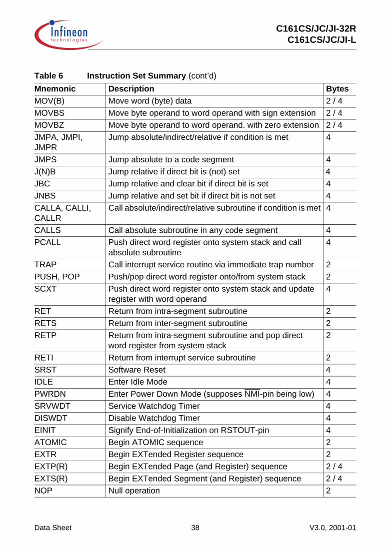
MOV(B) Move word (byte) data 2 / 4
MOVBS Move byte operand to word operand with sign extension 2 / 4MOVBZ Move byte operand to word operand. with zero extension 2 / 4
JMPA, JMPI, JMPR
Jump absolute/indirect/relative if condition is met 4
JMPS Jump absolute to a code segment 4
J(N)B Jump relative if direct bit is (not) set 4JBC Jump relative and clear bit if direct bit is set 4
JNBS Jump relative and set bit if direct bit is not set 4
CALLA, CALLI, CALLR
Call absolute/indirect/relative subroutine if condition is met 4
CALLS Call absolute subroutine in any code segment 4PCALL Push direct word register onto system stack and call
absolute subroutine4
TRAP Call interrupt service routine via immediate trap number 2
PUSH, POP Push/pop direct word register onto/from system stack 2
SCXT Push direct word register onto system stack and updateregister with word operand
4
RET Return from intra-segment subroutine 2RETS Return from inter-segment subroutine 2
RETP Return from intra-segment subroutine and pop directword register from system stack
2
RETI Return from interrupt service subroutine 2
SRST Software Reset 4IDLE Enter Idle Mode 4
PWRDN Enter Power Down Mode (supposes NMI-pin being low) 4
SRVWDT Service Watchdog Timer 4DISWDT Disable Watchdog Timer 4
EINIT Signify End-of-Initialization on RSTOUT-pin 4
ATOMIC Begin ATOMIC sequence 2EXTR Begin EXTended Register sequence 2
EXTP(R) Begin EXTended Page (and Register) sequence 2 / 4
EXTS(R) Begin EXTended Segment (and Register) sequence 2 / 4NOP Null operation 2
Table 6 Instruction Set Summary (cont’d)
Mnemonic Description Bytes
Data Sheet 38 V3.0, 2001-01

C161CS/JC/JI-32RC161CS/JC/JI-L
Special Function Registers Overview
Table 7 lists all SFRs which are implemented in the C161CS/JC/JI in alphabetical order.Bit-addressable SFRs are marked with the letter “b” in column “Name”. SFRs within theExtended SFR-Space (ESFRs) are marked with the letter “E” in column “PhysicalAddress”. Registers within on-chip X-peripherals are marked with the letter “X” in column“Physical Address”.
An SFR can be specified via its individual mnemonic name. Depending on the selectedaddressing mode, an SFR can be accessed via its physical address (using the DataPage Pointers), or via its short 8-bit address (without using the Data Page Pointers).
Note: Registers within device specific interface modules (CAN, SDLM) are only presentin the corresponding device, of course.
Table 7 C161CS/JC/JI Registers, Ordered by Name
Name PhysicalAddress
8-BitAddr.
Description ResetValue
ADCIC b FF98H CCH A/D Converter End of Conversion Interrupt Control Register
0000H
ADCON b FFA0H D0H A/D Converter Control Register 0000H
ADDAT FEA0H 50H A/D Converter Result Register 0000H
ADDAT2 F0A0H E 50H A/D Converter 2 Result Register 0000H
ADDRSEL1 FE18H 0CH Address Select Register 1 0000H
ADDRSEL2 FE1AH 0DH Address Select Register 2 0000H
ADDRSEL3 FE1CH 0EH Address Select Register 3 0000H
ADDRSEL4 FE1EH 0FH Address Select Register 4 0000H
ADEIC b FF9AH CDH A/D Converter Overrun Error Interrupt Control Register
0000H
BUFFCON EB24H X --- SDLM Buffer Control Register 0000H
BUFFSTAT EB1CH X --- SDLM Buffer Status Register 0000H
BUSCON0 b FF0CH 86H Bus Configuration Register 0 0000H
BUSCON1 b FF14H 8AH Bus Configuration Register 1 0000H
BUSCON2 b FF16H 8BH Bus Configuration Register 2 0000H
BUSCON3 b FF18H 8CH Bus Configuration Register 3 0000H
BUSCON4 b FF1AH 8DH Bus Configuration Register 4 0000H
BUSSTAT EB20H X --- SDLM Bus Status Register 0000H
C1BTR EF04H X --- CAN1 Bit Timing Register UUUUH
C1CSR EF00H X --- CAN1 Control / Status Register XX01H
C1GMS EF06H X --- CAN1 Global Mask Short UFUUH
Data Sheet 39 V3.0, 2001-01

C161CS/JC/JI-32RC161CS/JC/JI-L
C1PCIR EF02H X --- CAN1 Port Control / Interrupt Register XXXXH
C1LARn EFn4H X --- CAN1 Lower Arbitration Reg. (msg. n) UUUUH
C1LGML EF0AH X --- CAN1 Lower Global Mask Long UUUUH
C1LMLM EF0EH X --- CAN1 Lower Mask of Last Message UUUUH
C1MCFGn EFn6H X --- CAN1 Message Config. Reg. (msg. n) UUH
C1MCRn EFn0H X --- CAN1 Message Control Reg. (msg. n) UUUUH
C1UARn EFn2H X --- CAN1 Upper Arbitration Reg. (msg. n) UUUUH
C1UGML EF08H X --- CAN1 Upper Global Mask Long UUUUH
C1UMLM EF0CH X --- CAN1 Upper Mask of Last Message UUUUH
C2BTR EE04H X --- CAN2 Bit Timing Register UUUUH
C2CSR EE00H X --- CAN2 Control / Status Register XX01H
C2GMS EE06H X --- CAN2 Global Mask Short UFUUH
C2PCIR EE02H X --- CAN2 Port Control / Interrupt Register XXXXH
C2LARn EEn4H X --- CAN2 Lower Arbitration Reg. (msg. n) UUUUH
C2LGML EE0AH X --- CAN2 Lower Global Mask Long UUUUH
C2LMLM EE0EH X --- CAN2 Lower Mask of Last Message UUUUH
C2MCFGn EEn6H X --- CAN2 Message Config. Reg. (msg. n) UUH
C2MCRn EEn0H X --- CAN2 Message Control Reg. (msg. n) UUUUH
C2UARn EEn2H X --- CAN2 Upper Arbitration Reg. (msg. n) UUUUH
C2UGML EE08H X --- CAN2 Upper Global Mask Long UUUUH
C2UMLM EE0CH X --- CAN2 Upper Mask of Last Message UUUUH
CAPREL FE4AH 25H GPT2 Capture/Reload Register 0000H
CC0 FE80H 40H CAPCOM Register 0 0000H
CC0IC b FF78H BCH CAPCOM Register 0 Interrupt Ctrl. Reg. 0000H
CC1 FE82H 41H CAPCOM Register 1 0000H
CC10 FE94H 4AH CAPCOM Register 10 0000H
CC10IC b FF8CH C6H CAPCOM Reg. 10 Interrupt Ctrl. Reg. 0000H
CC11 FE96H 4BH CAPCOM Register 11 0000H
CC11IC b FF8EH C7H CAPCOM Reg. 11 Interrupt Ctrl. Reg. 0000H
CC12 FE98H 4CH CAPCOM Register 12 0000H
CC12IC b FF90H C8H CAPCOM Reg. 12 Interrupt Ctrl. Reg. 0000H
CC13 FE9AH 4DH CAPCOM Register 13 0000H
Table 7 C161CS/JC/JI Registers, Ordered by Name (cont’d)
Name PhysicalAddress
8-BitAddr.
Description ResetValue
Data Sheet 40 V3.0, 2001-01
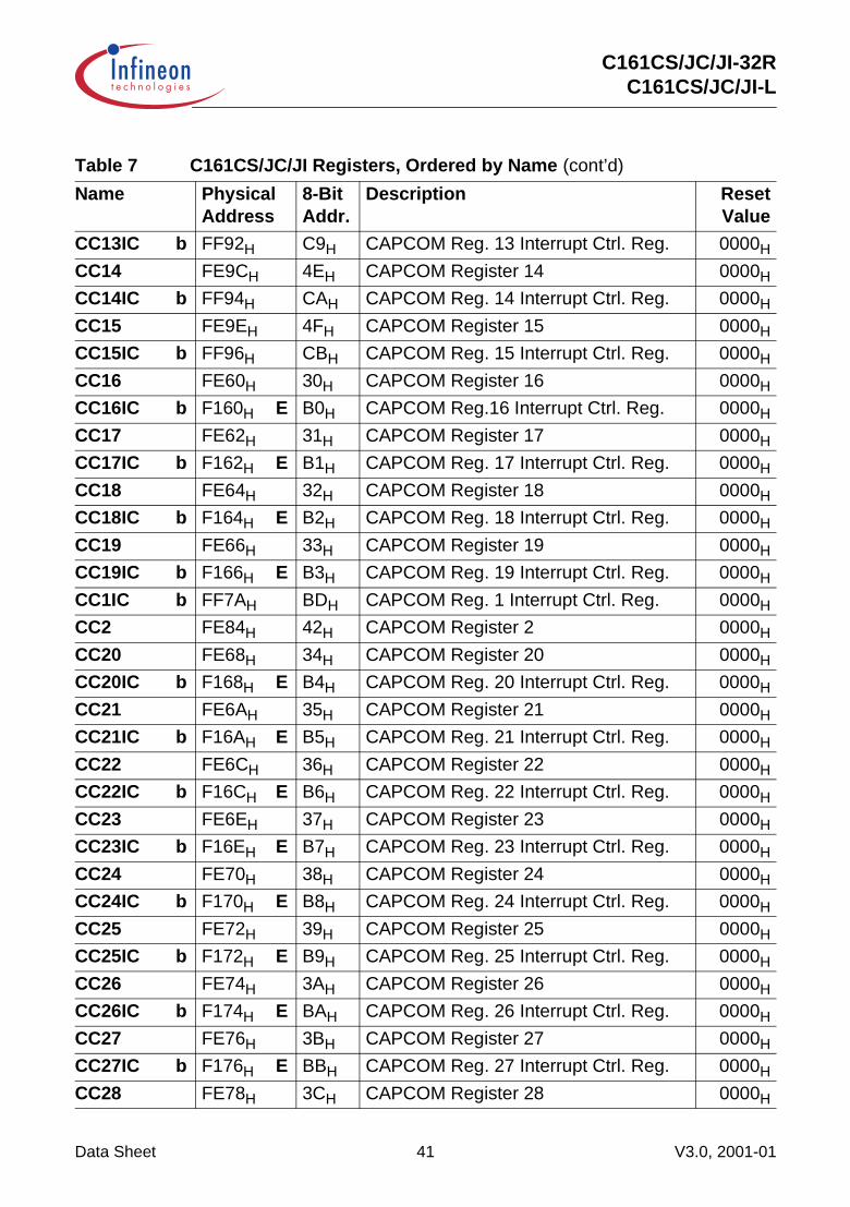
C161CS/JC/JI-32RC161CS/JC/JI-L
CC13IC b FF92H C9H CAPCOM Reg. 13 Interrupt Ctrl. Reg. 0000H
CC14 FE9CH 4EH CAPCOM Register 14 0000H
CC14IC b FF94H CAH CAPCOM Reg. 14 Interrupt Ctrl. Reg. 0000H
CC15 FE9EH 4FH CAPCOM Register 15 0000H
CC15IC b FF96H CBH CAPCOM Reg. 15 Interrupt Ctrl. Reg. 0000H
CC16 FE60H 30H CAPCOM Register 16 0000H
CC16IC b F160H E B0H CAPCOM Reg.16 Interrupt Ctrl. Reg. 0000H
CC17 FE62H 31H CAPCOM Register 17 0000H
CC17IC b F162H E B1H CAPCOM Reg. 17 Interrupt Ctrl. Reg. 0000H
CC18 FE64H 32H CAPCOM Register 18 0000H
CC18IC b F164H E B2H CAPCOM Reg. 18 Interrupt Ctrl. Reg. 0000H
CC19 FE66H 33H CAPCOM Register 19 0000H
CC19IC b F166H E B3H CAPCOM Reg. 19 Interrupt Ctrl. Reg. 0000H
CC1IC b FF7AH BDH CAPCOM Reg. 1 Interrupt Ctrl. Reg. 0000H
CC2 FE84H 42H CAPCOM Register 2 0000H
CC20 FE68H 34H CAPCOM Register 20 0000H
CC20IC b F168H E B4H CAPCOM Reg. 20 Interrupt Ctrl. Reg. 0000H
CC21 FE6AH 35H CAPCOM Register 21 0000H
CC21IC b F16AH E B5H CAPCOM Reg. 21 Interrupt Ctrl. Reg. 0000H
CC22 FE6CH 36H CAPCOM Register 22 0000H
CC22IC b F16CH E B6H CAPCOM Reg. 22 Interrupt Ctrl. Reg. 0000H
CC23 FE6EH 37H CAPCOM Register 23 0000H
CC23IC b F16EH E B7H CAPCOM Reg. 23 Interrupt Ctrl. Reg. 0000H
CC24 FE70H 38H CAPCOM Register 24 0000H
CC24IC b F170H E B8H CAPCOM Reg. 24 Interrupt Ctrl. Reg. 0000H
CC25 FE72H 39H CAPCOM Register 25 0000H
CC25IC b F172H E B9H CAPCOM Reg. 25 Interrupt Ctrl. Reg. 0000H
CC26 FE74H 3AH CAPCOM Register 26 0000H
CC26IC b F174H E BAH CAPCOM Reg. 26 Interrupt Ctrl. Reg. 0000H
CC27 FE76H 3BH CAPCOM Register 27 0000H
CC27IC b F176H E BBH CAPCOM Reg. 27 Interrupt Ctrl. Reg. 0000H
CC28 FE78H 3CH CAPCOM Register 28 0000H
Table 7 C161CS/JC/JI Registers, Ordered by Name (cont’d)
Name PhysicalAddress
8-BitAddr.
Description ResetValue
Data Sheet 41 V3.0, 2001-01

C161CS/JC/JI-32RC161CS/JC/JI-L
CC28IC b F178H E BCH CAPCOM Reg. 28 Interrupt Ctrl. Reg. 0000H
CC29 FE7AH 3DH CAPCOM Register 29 0000H
CC29IC b F184H E C2H CAPCOM Reg. 29 Interrupt Ctrl. Reg. 0000H
CC2IC b FF7CH BEH CAPCOM Reg. 2 Interrupt Ctrl. Reg. 0000H
CC3 FE86H 43H CAPCOM Register 3 0000H
CC30 FE7CH 3EH CAPCOM Register 30 0000H
CC30IC b F18CH E C6H CAPCOM Reg. 30 Interrupt Ctrl. Reg. 0000H
CC31 FE7EH 3FH CAPCOM Register 31 0000H
CC31IC b F194H E CAH CAPCOM Reg. 31 Interrupt Ctrl. Reg. 0000H
CC3IC b FF7EH BFH CAPCOM Reg. 3 Interrupt Ctrl. Reg. 0000H
CC4 FE88H 44H CAPCOM Register 4 0000H
CC4IC b FF80H C0H CAPCOM Reg. 4 Interrupt Ctrl. Reg. 0000H
CC5 FE8AH 45H CAPCOM Register 5 0000H
CC5IC b FF82H C1H CAPCOM Reg. 5 Interrupt Ctrl. Reg. 0000H
CC6 FE8CH 46H CAPCOM Register 6 0000H
CC6IC b FF84H C2H CAPCOM Reg. 6 Interrupt Ctrl. Reg. 0000H
CC7 FE8EH 47H CAPCOM Register 7 0000H
CC7IC b FF86H C3H CAPCOM Reg. 7 Interrupt Ctrl. Reg. 0000H
CC8 FE90H 48H CAPCOM Register 8 0000H
CC8IC b FF88H C4H CAPCOM Reg. 8 Interrupt Ctrl. Reg. 0000H
CC9 FE92H 49H CAPCOM Register 9 0000H
CC9IC b FF8AH C5H CAPCOM Reg. 9 Interrupt Ctrl. Reg. 0000H
CCM0 b FF52H A9H CAPCOM Mode Control Register 0 0000H
CCM1 b FF54H AAH CAPCOM Mode Control Register 1 0000H
CCM2 b FF56H ABH CAPCOM Mode Control Register 2 0000H
CCM3 b FF58H ACH CAPCOM Mode Control Register 3 0000H
CCM4 b FF22H 91H CAPCOM Mode Control Register 4 0000H
CCM5 b FF24H 92H CAPCOM Mode Control Register 5 0000H
CCM6 b FF26H 93H CAPCOM Mode Control Register 6 0000H
CCM7 b FF28H 94H CAPCOM Mode Control Register 7 0000H
CLKDIV EB14H X --- SDLM Clock Divider Register 0000H
CP FE10H 08H CPU Context Pointer Register FC00H
Table 7 C161CS/JC/JI Registers, Ordered by Name (cont’d)
Name PhysicalAddress
8-BitAddr.
Description ResetValue
Data Sheet 42 V3.0, 2001-01

C161CS/JC/JI-32RC161CS/JC/JI-L
CRIC b FF6AH B5H GPT2 CAPREL Interrupt Ctrl. Reg. 0000H
CSP FE08H 04H CPU Code Segment Pointer Register(8 bits, not directly writeable)
0000H
DP0H b F102H E 81H P0H Direction Control Register 00H
DP0L b F100H E 80H P0L Direction Control Register 00H
DP1H b F106H E 83H P1H Direction Control Register 00H
DP1L b F104H E 82H P1L Direction Control Register 00H
DP2 b FFC2H E1H Port 2 Direction Control Register 0000H
DP3 b FFC6H E3H Port 3 Direction Control Register 0000H
DP4 b FFCAH E5H Port 4 Direction Control Register 00H
DP6 b FFCEH E7H Port 6 Direction Control Register 00H
DP7 b FFD2H E9H Port 7 Direction Control Register 00H
DP9 b FFDAH EDH Port 9 Direction Control Register 00H
DPP0 FE00H 00H CPU Data Page Pointer 0 Reg. (10 bits) 0000H
DPP1 FE02H 01H CPU Data Page Pointer 1 Reg. (10 bits) 0001H
DPP2 FE04H 02H CPU Data Page Pointer 2 Reg. (10 bits) 0002H
DPP3 FE06H 03H CPU Data Page Pointer 3 Reg. (10 bits) 0003H
ERRSTAT EB22H X --- SDLM Error Status Register 0000H
EXICON b F1C0H E E0H External Interrupt Control Register 0000H
EXISEL b F1DAH E EDH External Interrupt Source Select Register
0000H
FLAGRST EB28H X --- SDLM Flag Reset Register 0000H
FOCON b FFAAH D5H Frequency Output Control Register 0000H
GLOBCON EB10H X --- SDLM Global Control Register 0000H
ICADR ED06H X --- IIC Address Register 0XXXH
ICCFG ED00H X --- IIC Configuration Register XX00H
ICCON ED02H X --- IIC Control Register 0000H
ICRTB ED08H X --- IIC Receive/Transmit Buffer XXH
ICST ED04H X --- IIC Status Register 0000H
IDCHIP F07CH E 3EH Identifier 1XXXH
IDMANUF F07EH E 3FH Identifier 1820H
IDMEM F07AH E 3DH Identifier X040H
Table 7 C161CS/JC/JI Registers, Ordered by Name (cont’d)
Name PhysicalAddress
8-BitAddr.
Description ResetValue
Data Sheet 43 V3.0, 2001-01
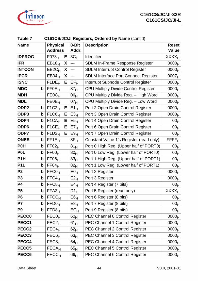
C161CS/JC/JI-32RC161CS/JC/JI-L
IDPROG F078H E 3CH Identifier XXXXH
IFR EB18H X --- SDLM In-Frame Response Register 0000H
INTCON EB2CH X --- SDLM Interrupt Control Register 0000H
IPCR EB04H X --- SDLM Interface Port Connect Register 0007H
ISNC F1DEH E EFH Interrupt Subnode Control Register 0000H
MDC b FF0EH 87H CPU Multiply Divide Control Register 0000H
MDH FE0CH 06H CPU Multiply Divide Reg. – High Word 0000H
MDL FE0EH 07H CPU Multiply Divide Reg. – Low Word 0000H
ODP2 b F1C2H E E1H Port 2 Open Drain Control Register 0000H
ODP3 b F1C6H E E3H Port 3 Open Drain Control Register 0000H
ODP4 b F1CAH E E5H Port 4 Open Drain Control Register 00H
ODP6 b F1CEH E E7H Port 6 Open Drain Control Register 00H
ODP7 b F1D2H E E9H Port 7 Open Drain Control Register 00H
ONES b FF1EH 8FH Constant Value 1’s Register (read only) FFFFH
P0H b FF02H 81H Port 0 High Reg. (Upper half of PORT0) 00H
P0L b FF00H 80H Port 0 Low Reg. (Lower half of PORT0) 00H
P1H b FF06H 83H Port 1 High Reg. (Upper half of PORT1) 00H
P1L b FF04H 82H Port 1 Low Reg. (Lower half of PORT1) 00H
P2 b FFC0H E0H Port 2 Register 0000H
P3 b FFC4H E2H Port 3 Register 0000H
P4 b FFC8H E4H Port 4 Register (7 bits) 00H
P5 b FFA2H D1H Port 5 Register (read only) XXXXH
P6 b FFCCH E6H Port 6 Register (8 bits) 00H
P7 b FFD0H E8H Port 7 Register (8 bits) 00H
P9 b FFD8H ECH Port 9 Register (8 bits) 00H
PECC0 FEC0H 60H PEC Channel 0 Control Register 0000H
PECC1 FEC2H 61H PEC Channel 1 Control Register 0000H
PECC2 FEC4H 62H PEC Channel 2 Control Register 0000H
PECC3 FEC6H 63H PEC Channel 3 Control Register 0000H
PECC4 FEC8H 64H PEC Channel 4 Control Register 0000H
PECC5 FECAH 65H PEC Channel 5 Control Register 0000H
PECC6 FECCH 66H PEC Channel 6 Control Register 0000H
Table 7 C161CS/JC/JI Registers, Ordered by Name (cont’d)
Name PhysicalAddress
8-BitAddr.
Description ResetValue
Data Sheet 44 V3.0, 2001-01

C161CS/JC/JI-32RC161CS/JC/JI-L
PECC7 FECEH 67H PEC Channel 7 Control Register 0000H
PICON b F1C4H E E2H Port Input Threshold Control Register 0000H
POCON0H F082H E 41H P0L Output Control Register 0000H
POCON0L F080H E 40H P0H Output Control Register 0000H
POCON1H F086H E 43H P1L Output Control Register 0000H
POCON1L F084H E 42H P1H Output Control Register 0000H
POCON2 F088H E 44H Port 2 Output Control Register 0000H
POCON20 F0AAH E 55H Dedicated Pins Output Control Register 0000H
POCON3 F08AH E 45H Port 3 Output Control Register 0000H
POCON4 F08CH E 46H Port 4 Output Control Register 0000H
POCON6 F08EH E 47H Port 6 Output Control Register 0000H
POCON7 F090H E 48H Port 7 Output Control Register 0000H
PSW b FF10H 88H CPU Program Status Word 0000H
RP0H b F108H E 84H System Startup Configuration Register (Rd. only)
XXH
RSTCON b F1E0H m --- Reset Control Register 00XXH
RTCH F0D6H E 6BH RTC High Register no
RTCL F0D4H E 6AH RTC Low Register no
RXCNT EB4CH X --- SDLM Bus Receive Byte Counter (CPU) 0000H
RXCNTB EB4AH X --- SDLM Bus Receive Byte Counter (bus) 0000H
RXCPU EB4EH X --- SDLM CPU Receive Byte Counter Reg. 0000H
RXD00 EB40H X --- SDLM Receive Data Register 00 (CPU) 0000H
RXD010 EB4AH X --- SDLM Receive Data Register 010 (CPU) 0000H
RXD02 EB42H X --- SDLM Receive Data Register 02 (CPU) 0000H
RXD04 EB44H X --- SDLM Receive Data Register 04 (CPU) 0000H
RXD06 EB46H X --- SDLM Receive Data Register 06 (CPU) 0000H
RXD08 EB48H X --- SDLM Receive Data Register 08 (CPU) 0000H
RXD10 EB50H X --- SDLM Receive Data Register 10 (bus) 0000H
RXD110 EB5AH X --- SDLM Receive Data Register 110 (bus) 0000H
RXD12 EB52H X --- SDLM Receive Data Register 12 (bus) 0000H
RXD14 EB54H X --- SDLM Receive Data Register 14 (bus) 0000H
RXD16 EB56H X --- SDLM Receive Data Register 16 (bus) 0000H
Table 7 C161CS/JC/JI Registers, Ordered by Name (cont’d)
Name PhysicalAddress
8-BitAddr.
Description ResetValue
Data Sheet 45 V3.0, 2001-01

C161CS/JC/JI-32RC161CS/JC/JI-L
RXD18 EB58H X --- SDLM Receive Data Register 18 (bus) 0000H
S0BG FEB4H 5AH Serial Channel 0 Baud Rate Generator Reload Register
0000H
S0CON b FFB0H D8H Serial Channel 0 Control Register 0000H
S0EIC b FF70H B8H Serial Channel 0 Error Interrupt Ctrl. Reg.
0000H
S0RBUF FEB2H 59H Serial Channel 0 Receive Buffer Register (read only)
XXXXH
S0RIC b FF6EH B7H Serial Channel 0 Receive Interrupt Control Register
0000H
S0TBIC b F19CH E CEH Serial Channel 0 Transmit Buffer Interrupt Control Register
0000H
S0TBUF FEB0H 58H Serial Channel 0 Transmit Buffer Register
0000H
S0TIC b FF6CH B6H Serial Channel 0 Transmit Interrupt Control Register
0000H
S1BG EDA4H X --- Serial Channel 1 Baud Rate Generator Reload Register
0000H
S1CON EDA6H X --- Serial Channel 1 Control Register 0000H
S1RBUF EDA2H X --- Serial Channel 1 Receive Buffer Register (read only)
XXXXH
S1TBUF EDA0H X --- Serial Channel 1 Transmit Buffer Register
0000H
SOFPTR EB60H X --- SDLM Start-of-Frame Pointer Register 0000H
SP FE12H 09H CPU System Stack Pointer Register FC00H
SSCBR F0B4H E 5AH SSC Baudrate Register 0000H
SSCCON b FFB2H D9H SSC Control Register 0000H
SSCEIC b FF76H BBH SSC Error Interrupt Control Register 0000H
SSCRB F0B2H E 59H SSC Receive Buffer (read only) XXXXH
SSCRIC b FF74H BAH SSC Receive Interrupt Control Register 0000H
SSCTB F0B0H E 58H SSC Transmit Buffer (write only) 0000H
SSCTIC b FF72H B9H SSC Transmit Interrupt Control Register 0000H
STKOV FE14H 0AH CPU Stack Overflow Pointer Register FA00H
STKUN FE16H 0BH CPU Stack Underflow Pointer Register FC00H
Table 7 C161CS/JC/JI Registers, Ordered by Name (cont’d)
Name PhysicalAddress
8-BitAddr.
Description ResetValue
Data Sheet 46 V3.0, 2001-01

C161CS/JC/JI-32RC161CS/JC/JI-L
SYSCON b FF12H 89H CPU System Configuration Register 1)0XX0H
SYSCON1 b F1DCH E EEH CPU System Configuration Register 1 0000H
SYSCON2 b F1D0H E E8H CPU System Configuration Register 2 0000H
SYSCON3 b F1D4H E EAH CPU System Configuration Register 3 0X00H
T0 FE50H 28H CAPCOM Timer 0 Register 0000H
T01CON b FF50H A8H CAPCOM Timer 0 and Timer 1 Ctrl. Reg. 0000H
T0IC b FF9CH CEH CAPCOM Timer 0 Interrupt Ctrl. Reg. 0000H
T0REL FE54H 2AH CAPCOM Timer 0 Reload Register 0000H
T1 FE52H 29H CAPCOM Timer 1 Register 0000H
T14 F0D2H E 69H RTC Timer 14 Register no
T14REL F0D0H E 68H RTC Timer 14 Reload Register no
T1IC b FF9EH CFH CAPCOM Timer 1 Interrupt Ctrl. Reg. 0000H
T1REL FE56H 2BH CAPCOM Timer 1 Reload Register 0000H
T2 FE40H 20H GPT1 Timer 2 Register 0000H
T2CON b FF40H A0H GPT1 Timer 2 Control Register 0000H
T2IC b FF60H B0H GPT1 Timer 2 Interrupt Control Register 0000H
T3 FE42H 21H GPT1 Timer 3 Register 0000H
T3CON b FF42H A1H GPT1 Timer 3 Control Register 0000H
T3IC b FF62H B1H GPT1 Timer 3 Interrupt Control Register 0000H
T4 FE44H 22H GPT1 Timer 4 Register 0000H
T4CON b FF44H A2H GPT1 Timer 4 Control Register 0000H
T4IC b FF64H B2H GPT1 Timer 4 Interrupt Control Register 0000H
T5 FE46H 23H GPT2 Timer 5 Register 0000H
T5CON b FF46H A3H GPT2 Timer 5 Control Register 0000H
T5IC b FF66H B3H GPT2 Timer 5 Interrupt Control Register 0000H
T6 FE48H 24H GPT2 Timer 6 Register 0000H
T6CON b FF48H A4H GPT2 Timer 6 Control Register 0000H
T6IC b FF68H B4H GPT2 Timer 6 Interrupt Control Register 0000H
T7 F050H E 28H CAPCOM Timer 7 Register 0000H
T78CON b FF20H 90H CAPCOM Timer 7 and 8 Ctrl. Reg. 0000H
T7IC b F17AH E BDH CAPCOM Timer 7 Interrupt Ctrl. Reg. 0000H
T7REL F054H E 2AH CAPCOM Timer 7 Reload Register 0000H
Table 7 C161CS/JC/JI Registers, Ordered by Name (cont’d)
Name PhysicalAddress
8-BitAddr.
Description ResetValue
Data Sheet 47 V3.0, 2001-01

C161CS/JC/JI-32RC161CS/JC/JI-L
T8 F052H E 29H CAPCOM Timer 8 Register 0000H
T8IC b F17CH E BEH CAPCOM Timer 8 Interrupt Ctrl. Reg. 0000H
T8REL F056H E 2BH CAPCOM Timer 8 Reload Register 0000H
TFR b FFACH D6H Trap Flag Register 0000H
TRANSSTAT EB1EH X --- SDLM Transmission Status Register 0000H
TXCNT EB3CH X --- SDLM Bus Transmit Byte Counter Reg. 0000H
TXCPU EB3EH X --- SDLM CPU Transmit Byte Counter Reg. 0000H
TXD0 EB30H X --- SDLM Transmit Data Register 0 0000H
TXD10 EB3AH X --- SDLM Transmit Data Register 10 0000H
TXD2 EB32H X --- SDLM Transmit Data Register 2 0000H
TXD4 EB34H X --- SDLM Transmit Data Register 4 0000H
TXD6 EB36H X --- SDLM Transmit Data Register 6 0000H
TXD8 EB38H X --- SDLM Transmit Data Register 8 0000H
TxDELAY EB16H X --- SDLM Transceiver Delay Register 0014H
WDT FEAEH 57H Watchdog Timer Register (read only) 0000H
WDTCON b FFAEH D7H Watchdog Timer Control Register 2)00XXH
XP0IC b F186H E C3H IIC Data Interrupt Control Register 0000H
XP1IC b F18EH E C7H IIC Protocol Interrupt Control Register 0000H
XP2IC b F196H E CBH CAN1 Interrupt Control Register 0000H
XP3IC b F19EH E CFH PLL/RTC Interrupt Control Register 0000H
XP4IC b F182H E C1H ASC1 Transmit Interrupt Ctrl. Reg. 0000H
XP5IC b F18AH E C5H ASC1 Receive Interrupt Control Register 0000H
XP6IC b F192H E C9H ASC1 Error Interrupt Control Register 0000H
XP7IC b F19AH E CDH CAN2/SDLM Interrupt Control Register 0000H
ZEROS b FF1CH 8EH Constant Value 0’s Register (read only) 0000H
1) The system configuration is selected during reset.2) The reset value depends on the indicated reset source.
Table 7 C161CS/JC/JI Registers, Ordered by Name (cont’d)
Name PhysicalAddress
8-BitAddr.
Description ResetValue
Data Sheet 48 V3.0, 2001-01

C161CS/JC/JI-32RC161CS/JC/JI-L
Absolute Maximum Ratings
Note: Stresses above those listed under “Absolute Maximum Ratings” may causepermanent damage to the device. This is a stress rating only and functionaloperation of the device at these or any other conditions above those indicated inthe operational sections of this specification is not implied. Exposure to absolutemaximum rating conditions for extended periods may affect device reliability.During absolute maximum rating overload conditions (VIN > VDD or VIN < VSS) thevoltage on VDD pins with respect to ground (VSS) must not exceed the valuesdefined by the absolute maximum ratings.
Table 8 Absolute Maximum Rating Parameters
Parameter Symbol Limit Values Unit Notes
min. max.
Storage temperature TST -65 150 °C –
Junction temperature TJ -40 150 °C under bias
Voltage on VDD pins with respect to ground (VSS)
VDD -0.5 6.5 V –
Voltage on any pin with respect to ground (VSS)
VIN -0.5 VDD + 0.5 V –
Input current on any pin during overload condition
– -10 10 mA –
Absolute sum of all input currents during overload condition
– – |100| mA –
Power dissipation PDISS – 1.5 W –
Data Sheet 49 V3.0, 2001-01

C161CS/JC/JI-32RC161CS/JC/JI-L
Operating Conditions
The following operating conditions must not be exceeded in order to ensure correctoperation of the C161CS/JC/JI. All parameters specified in the following sections referto these operating conditions, unless otherwise noticed.
Table 9 Operating Condition Parameters
Parameter Symbol Limit Values Unit Notes
min. max.
Digital supply voltage VDD 4.5 5.5 V Active mode,fCPUmax = 25 MHz
2.51)
1) Output voltages and output currents will be reduced when VDD leaves the range defined for active mode.
5.5 V PowerDown mode
Digital ground voltage VSS 0 V Reference voltage
Overload current IOV – ±5 mA Per pin2)3)4)
2) Overload conditions occur if the standard operatings conditions are exceeded, i.e. the voltage on any pinexceeds the specified range (i.e. VOV > VDD + 0.5 V or VOV < VSS - 0.5 V). The absolute sum of input overloadcurrents on all pins may not exceed 50 mA. The supply voltage must remain within the specified limits.Proper operation is not guaranteed if overload conditions occur on functional pins line XTAL1, RD, WR, etc.
3) Not 100% tested, guaranteed by design and characterization.4) Due to the different port structure of Port 9 (required by the IIC bus specification) the pins of Port 9 can only
tolerate positive overload current, i.e. VOV > VSS - 0.5 V.
Absolute sum of overload currents
Σ|IOV| – 50 mA 3)
External Load Capacitance
CL – 100 pF Pin drivers infast edge mode5)
5) The timing is valid for pin drivers in high current or dynamic current mode. The reduced static output currentin dynamic current mode must be respected when designing the system.
Ambient temperature TA 0 70 °C SAB-C161CS/JC/JI …
-40 85 °C SAF-C161CS/JC/JI …
-40 125 °C SAK-C161CS/JC/JI …
Data Sheet 50 V3.0, 2001-01

C161CS/JC/JI-32RC161CS/JC/JI-L
Parameter Interpretation
The parameters listed in the following partly represent the characteristics of the C161CS/JC/JI and partly its demands on the system. To aid in interpreting the parameters right,when evaluating them for a design, they are marked in column “Symbol”:
CC (Controller Characteristics):The logic of the C161CS/JC/JI will provide signals with the respective timingcharacteristics.
SR (System Requirement):The external system must provide signals with the respective timing characteristics tothe C161CS/JC/JI.
DC Characteristics(Operating Conditions apply)1)
Parameter Symbol Limit Values Unit Test Condition
min. max.
Input low voltage (TTL,all except XTAL1, XTAL3, Port 9)
VIL SR -0.5 0.2 VDD- 0.1
V –
Input low voltageXTAL1, XTAL3, Port 9
VIL2 SR -0.5 0.3 VDD V –
Input low voltage(Special Threshold)
VILS SR -0.5 2.0 V –
Input high voltage (TTL, all except RSTIN, XTAL1, XTAL3, Port 9)
VIH SR 0.2 VDD+ 0.9
VDD + 0.5
V –
Input high voltage RSTIN(when operated as input)
VIH1 SR 0.6 VDD VDD + 0.5
V –
Input high voltageXTAL1, XTAL3, Port 9
VIH2 SR 0.7 VDD VDD + 0.5
V –
Input high voltage(Special Threshold)
VIHS SR 0.8 VDD- 0.2
VDD + 0.5
V –
Input Hysteresis(Special Threshold)
HYS 400 – mV Series resistance = 0 Ω
Output low voltage(PORT0, PORT1, Port 4, ALE, RD, WR, BHE, CLKOUT, RSTOUT, RSTIN2))
VOL CC – 0.45 V IOL = 2.4 mA3)
IOL = 0.5 mA4)
Output low voltage(Port 9)
VOL9 CC – 0.4 V IOL = 3.0 mA
Data Sheet 51 V3.0, 2001-01

C161CS/JC/JI-32RC161CS/JC/JI-L
Output low voltage(all other outputs)
VOL1 CC – 0.45 V IOL = 1.6 mA3)
IOL = 1.6 mA4)
Output high voltage5)
(PORT0, PORT1, Port 4, ALE, RD, WR, BHE, CLKOUT, RSTOUT)
VOH CC 2.4 – V IOH = -2.4 mA3)
IOH = -0.5 mA4)
0.9 VDD – V IOH = -0.5 mA3)
Output high voltage5)
(all other outputs)VOH1 CC 2.4 – V IOH = -1.6 mA3)
IOH = -0.5 mA4)
0.9 VDD – V IOH = -0.5 mA3)
Input leakage current (Port 5) IOZ1 CC – ±200 nA 0 V < VIN < VDD
Input leakage current (all other) IOZ2 CC – ±500 nA 0.45 V < VIN < VDD
RSTIN inactive current6) IRSTH7) – -10 µA VIN = VIH1
RSTIN active current6) IRSTL8) -100 – µA VIN = VIL
READY/RD/WR inact. current9) IRWH 7) – -40 µA VOUT = 2.4 V
READY/RD/WR active current9) IRWL8) -500 – µA VOUT = VOLmax
ALE inactive current9) IALEL7) – 40 µA VOUT = VOLmax
ALE active current9) IALEH8) 500 – µA VOUT = 2.4 V
Port 6 inactive current9) IP6H7) – -40 µA VOUT = 2.4 V
Port 6 active current9) IP6L8) -500 – µA VOUT = VOL1max
PORT0 configuration current10) IP0H7) – -10 µA VIN = VIHmin
IP0L8) -100 – µA VIN = VILmax
XTAL1 input current IIL CC – ±20 µA 0 V < VIN < VDD
Pin capacitance11) (digital inputs/outputs)
CIO CC – 10 pF f = 1 MHzTA = 25 °C
1) Keeping signal levels within the levels specified in this table, ensures operation without overload conditions.For signal levels outside these specifications also refer to the specification of the overload current IOV.
2) Valid in bidirectional reset mode only.3) This output current may be drawn from (output) pins operating in High Current mode.4) This output current may be drawn from (output) pins operating in Low Current mode.5) This specification is not valid for outputs which are switched to open drain mode. In this case the respective
output will float and the voltage results from the external circuitry.
DC Characteristics (cont’d)(Operating Conditions apply)1)
Parameter Symbol Limit Values Unit Test Condition
min. max.
Data Sheet 52 V3.0, 2001-01

C161CS/JC/JI-32RC161CS/JC/JI-L
6) These parameters describe the RSTIN pullup, which equals a resistance of ca. 50 to 250 kΩ.7) The maximum current may be drawn while the respective signal line remains inactive.8) The minimum current must be drawn in order to drive the respective signal line active.9) This specification is valid during Reset and during Hold-mode or Adapt-mode. During Hold-mode Port 6 pins
are only affected, if they are used (configured) for CS output and the open drain function is not enabled. TheREADY-pullup is always active, except for Powerdown mode.
10) This specification is valid during Reset and during Adapt-mode.11) Not 100% tested, guaranteed by design and characterization.
Power Consumption C161CS/JC/JI(Operating Conditions apply)
Parameter Symbol Limit Values Unit Test Condition
min. max.
Power supply current (active)with all peripherals active
IDD – 15 +2.5 × fCPU
mA RSTIN = VILfCPU in [MHz]1)
1) The supply current is a function of the operating frequency. This dependency is illustrated in Figure 10.These parameters are tested at VDDmax and maximum CPU clock with all outputs disconnected and all inputsat VIL or VIH.
Idle mode supply currentwith all peripherals active
IIDX – 5 +1.5 × fCPU
mA RSTIN = VIH1fCPU in [MHz]1)
Idle mode supply curr., Main osc,with all peripherals deactivated, PLL off, SDD factor = 32
IIDOM2)
2) This parameter is determined mainly by the current consumed by the oscillator (see Figure 9). This current,however, is influenced by the external oscillator circuitry (crystal, capacitors). The values given refer to a typicalcircuitry and may change in case of a not optimized external oscillator circuitry.
– 500 +50 × fOSC
µA RSTIN = VIH1fOSC in [MHz]1)
Idle mode supply curr., Aux. osc,with all peripherals deactivated, PLL off, SDD factor = 32
IIDOA2) – 100 µA VDD = VDDmax
fOSC = 32 kHz3)
3) This parameter is tested including leakage currents. All inputs (including pins configured as inputs) at 0 V to0.1 V or at VDD - 0.1 V to VDD, all outputs (including pins configured as outputs) disconnected.
Sleep and Power-down mode supply current with RTC running on main oscillator
IPDRM2) – 200 +
25 × fOSC
µA VDD = VDDmaxfOSC in [MHz]3)
Sleep and Power-down mode supply current with RTC disabled
IPDO – 50 µA VDD = VDDmax3)
Data Sheet 53 V3.0, 2001-01

C161CS/JC/JI-32RC161CS/JC/JI-L
Figure 9 Idle and Power Down Supply Current as a Function of Oscillator Frequency
MCD04453
fOSC
0
µA
0 4 8 12 16
250
500
750
1000
1250
1500
MHz
I
I IDOMmax
I IDOMtyp
IPDRMmax
IPDOmaxIIDOAmax
Data Sheet 54 V3.0, 2001-01

C161CS/JC/JI-32RC161CS/JC/JI-L
Figure 10 Supply/Idle Current as a Function of Operating Frequency
I [mA]
fCPU [MHz]10 15 20 25
IDD5max
IDD5typ
IIDX5max
IIDX5typ
20
40
60
80
100
Data Sheet 55 V3.0, 2001-01

C161CS/JC/JI-32RC161CS/JC/JI-L
AC CharacteristicsDefinition of Internal Timing
The internal operation of the C161CS/JC/JI is controlled by the internal CPU clock fCPU.Both edges of the CPU clock can trigger internal (e.g. pipeline) or external (e.g. buscycles) operations.
The specification of the external timing (AC Characteristics) therefore depends on thetime between two consecutive edges of the CPU clock, called “TCL” (see Figure 11).
Figure 11 Generation Mechanisms for the CPU Clock
The CPU clock signal fCPU can be generated from the oscillator clock signal fOSC viadifferent mechanisms. The duration of TCLs and their variation (and also the derivedexternal timing) depends on the used mechanism to generate fCPU. This influence mustbe regarded when calculating the timings for the C161CS/JC/JI.
Note: The example for PLL operation shown in the fig. above refers to a PLL factor of 4.
The used mechanism to generate the basic CPU clock is selected by bitfield CLKCFGin register RP0H.7-5.Upon a long hardware reset register RP0H is loaded with the logic levels present on theupper half of PORT0 (P0H), i.e. bitfield CLKCFG represents the logic levels on pins
MCT04338
fOSC
fCPU
Phase Locked Loop Operation
TCL
fOSC
fCPU
Direct Clock Drive
fOSC
fCPU
Prescaler OperationTCL
TCL
TCL
TCL
TCL
Data Sheet 56 V3.0, 2001-01

C161CS/JC/JI-32RC161CS/JC/JI-L
P0.15-13 (P0H.7-5). Register RP0H can be loaded from the upper half of registerRSTCON under software control.
Table 10 associates the combinations of these three bits with the respective clockgeneration mode.
Prescaler Operation
When prescaler operation is configured (CLKCFG = 001B) the CPU clock is derived fromthe internal oscillator (input clock signal) by a 2:1 prescaler.The frequency of fCPU is half the frequency of fOSC and the high and low time of fCPU(i.e. the duration of an individual TCL) is defined by the period of the input clock fOSC.
The timings listed in the AC Characteristics that refer to TCLs therefore can becalculated using the period of fOSC for any TCL.
Phase Locked Loop
When PLL operation is configured (via CLKCFG) the on-chip phase locked loop isenabled and provides the CPU clock (see table above). The PLL multiplies the inputfrequency by the factor F which is selected via the combination of pins P0.15-13 (i.e.fCPU = fOSC × F). With every F’th transition of fOSC the PLL circuit synchronizes the CPUclock to the input clock. This synchronization is done smoothly, i.e. the CPU clockfrequency does not change abruptly.
Due to this adaptation to the input clock the frequency of fCPU is constantly adjusted soit is locked to fOSC. The slight variation causes a jitter of fCPU which also effects theduration of individual TCLs.
Table 10 C161CS/JC/JI Clock Generation Modes
CLKCFG(P0H.7-5)
CPU Frequency fCPU = fOSC × F
External Clock Input Range1)
1) The external clock input range refers to a CPU clock range of 10 … 25 MHz.
Notes
1 1 1 fOSC × 4 2.5 to 6.25 MHz Default configuration
1 1 0 fOSC × 3 3.33 to 8.33 MHz –
1 0 1 fOSC × 2 5 to 12.5 MHz –
1 0 0 fOSC × 5 2 to 5 MHz –
0 1 1 fOSC × 1 1 to 25 MHz Direct drive2)
2) The maximum frequency depends on the duty cycle of the external clock signal.
0 1 0 fOSC × 1.5 6.66 to 16.6 MHz –
0 0 1 fOSC / 2 2 to 50 MHz CPU clock via prescaler
0 0 0 fOSC × 2.5 4 to 10 MHz –
Data Sheet 57 V3.0, 2001-01

C161CS/JC/JI-32RC161CS/JC/JI-L
The timings listed in the AC Characteristics that refer to TCLs therefore must becalculated using the minimum TCL that is possible under the respective circumstances.
The actual minimum value for TCL depends on the jitter of the PLL. As the PLL isconstantly adjusting its output frequency so it corresponds to the applied input frequency(crystal or oscillator) the relative deviation for periods of more than one TCL is lower thanfor one single TCL (see formula and Figure 12).For a period of N × TCL the minimum value is computed using the correspondingdeviation DN:
(N × TCL)min = N × TCLNOM - DN DN [ns] = ±(13.3 + N × 6.3) / fCPU [MHz],
where N = number of consecutive TCLs and 1 ≤ N ≤ 40.
So for a period of 3 TCLs @ 25 MHz (i.e. N = 3): D3 = (13.3 + 3 × 6.3) / 25 = 1.288 ns,and (3TCL)min = 3TCLNOM - 1.288 ns = 58.7 ns (@ fCPU = 25 MHz).
This is especially important for bus cycles using waitstates and e.g. for the operation oftimers, serial interfaces, etc. For all slower operations and longer periods (e.g. pulsetrain generation or measurement, lower baudrates, etc.) the deviation caused by the PLLjitter is neglectible.
Note: For all periods longer than 40 TCL the N = 40 value can be used (see Figure 12).
Figure 12 Approximated Maximum Accumulated PLL Jitter
MCD04455
N
Max. jitter DN
±1
±10
±20
±30ns
±26.5
1 10 20 40
This approximated formula is valid for1 N 40 and 10 MHz fCPU 25 MHz.
10 MHz
16 MHz
20 MHz
25 MHz
30
<– <– <– <–
Data Sheet 58 V3.0, 2001-01

C161CS/JC/JI-32RC161CS/JC/JI-L
Direct Drive
When direct drive is configured (CLKCFG = 011B) the on-chip phase locked loop isdisabled and the CPU clock is directly driven from the internal oscillator with the inputclock signal.The frequency of fCPU directly follows the frequency of fOSC so the high and low time offCPU (i.e. the duration of an individual TCL) is defined by the duty cycle of the input clockfOSC.
The timings listed below that refer to TCLs therefore must be calculated using theminimum TCL that is possible under the respective circumstances. This minimum valuecan be calculated via the following formula:
TCLmin = 1/fOSC × DCmin (DC = duty cycle)
For two consecutive TCLs the deviation caused by the duty cycle of fOSC iscompensated so the duration of 2TCL is always 1/fOSC. The minimum value TCLmintherefore has to be used only once for timings that require an odd number of TCLs (1, 3,…). Timings that require an even number of TCLs (2, 4, …) may use the formula2TCL = 1/fOSC.
Note: The address float timings in Multiplexed bus mode (t11 and t45) use the maximumduration of TCL (TCLmax = 1/fOSC × DCmax) instead of TCLmin.
Data Sheet 59 V3.0, 2001-01

C161CS/JC/JI-32RC161CS/JC/JI-L
AC CharacteristicsExternal Clock Drive XTAL1 (Main Oscillator)
(Operating Conditions apply)
Figure 13 External Clock Drive XTAL1
Note: If the on-chip oscillator is used together with a crystal, the oscillator frequency islimited to a range of 4 MHz to 16 MHz.It is strongly recommended to measure the oscillation allowance (or margin) in thefinal target system (layout) to determine the optimum parameters for the oscillatoroperation. Please refer to the limits specified by the crystal supplier.When driven by an external clock signal it will accept the specified frequencyrange. Operation at lower input frequencies is possible but is guaranteed bydesign only (not 100% tested).
Table 11 External Clock Drive Characteristics
Parameter Symbol Direct Drive1:1
Prescaler2:1
PLL1:N
Unit
min. max. min. max. min. max.
Oscillator period tOSCM SR 40 – 20 – 601)
1) The minimum and maximum oscillator periods for PLL operation depend on the selected CPU clock generationmode. Please see respective table above.
5001) ns
High time2)
2) The clock input signal must reach the defined levels VIL2 and VIH2.
t1 SR 203)
3) The minimum high and low time refers to a duty cycle of 50%. The maximum operating frequency (fCPU) indirect drive mode depends on the duty cycle of the clock input signal.
– 6 – 10 – ns
Low time2) t2 SR 203) – 6 – 10 – ns
Rise time2) t3 SR – 10 – 6 – 10 ns
Fall time2) t4 SR – 10 – 6 – 10 ns
MCT02534
3t 4t
VIH2
VILVDD0.5
1t
2t
OSCt
Data Sheet 60 V3.0, 2001-01

C161CS/JC/JI-32RC161CS/JC/JI-L
AC CharacteristicsExternal Clock Drive XTAL3 (Auxiliary Oscillator)
(Operating Conditions apply)
Note: The auxiliary oscillator is optimized for oscillation with a crystal at a frequency of32 kHz. When driven by an external clock signal it will accept the specifiedfrequency range.Operation at lower input frequencies is possible but is guaranteed by design only(not 100% tested).
Table 12 AC Characteristics
Parameter Symbol Optimum Input Clock= 32 kHz
Variable Input Clock1 / tOSCA = 10 to 50 kHz
Unit
min. max. min. max.
Oscillator period tOSCA SR 31 31 20 100 µs
High time t1 SR 61)
1) The clock input signal must reach the defined levels VIL and VIH2.
– 0.2 × tOSCA1) – µs
Low time t2 SR 61) – 0.2 × tOSCA1) – µs
Rise time t3 SR – 12 – 0.4 × tOSCA µs
Fall time t4 SR – 12 – 0.4 × tOSCA µs
Data Sheet 61 V3.0, 2001-01

C161CS/JC/JI-32RC161CS/JC/JI-L
A/D Converter Characteristics
(Operating Conditions apply)
Table 13 A/D Converter Characteristics
Parameter Symbol Limit Values Unit Test Conditionmin. max.
Analog reference supply VAREF SR 4.0 VDD + 0.1 V 1)
1) TUE is tested at VAREF = 5.0 V, VAGND = 0 V, VDD = 4.9 V. It is guaranteed by design for all other voltageswithin the defined voltage range.If the analog reference supply voltage exceeds the power supply voltage by up to 0.2 V(i.e. VAREF = VDD = +0.2 V) the maximum TUE is increased to ±3 LSB. This range is not 100% tested.The specified TUE is guaranteed only if the absolute sum of input overload currents on Port 5 pins (see IOVspecification) does not exceed 10 mA.During the reset calibration sequence the maximum TUE may be ±4 LSB.
Analog reference ground VAGNDSR VSS - 0.1 VSS + 0.2 V
Analog input voltage range VAIN SR VAGND VAREF V 2)
2) VAIN may exceed VAGND or VAREF up to the absolute maximum ratings. However, the conversion result inthese cases will be X000H or X3FFH, respectively.
Basic clock frequency fBC 0.5 6.25 MHz 3)
3) The limit values for fBC must not be exceeded when selecting the CPU frequency and the ADCTC setting.
Conversion time tC CC – 40 tBC + tS + 2tCPU
– 4)
tCPU = 1 / fCPU
4) This parameter includes the sample time tS, the time for determining the digital result and the time to load theresult register with the conversion result.Values for the basic clock tBC depend on programming and can be taken from Table 14.This parameter depends on the ADC control logic. It is not a real maximum value, but rather a fixum.
Calibration time after reset tCAL CC – 3328 tBC – 5)
5) During the reset calibration conversions can be executed (with the current accuracy). The time required forthese conversions is added to the total reset calibration time.
Total unadjusted error TUE CC – ±2 LSB 1)
Internal resistance of reference voltage source
RAREF SR – tBC / 60- 0.25
kΩ tBC in [ns]6)7)
6) During the conversion the ADC’s capacitance must be repeatedly charged or discharged. The internalresistance of the reference voltage source must allow the capacitance to reach its respective voltage levelwithin each conversion step. The maximum internal resistance results from the programmed conversiontiming.
7) Not 100% tested, guaranteed by design and characterization.
Internal resistance of analog source
RASRC SR – tS / 450- 0.25
kΩ tS in [ns]7)8)
ADC input capacitance CAIN CC – 33 pF 7)
Data Sheet 62 V3.0, 2001-01

C161CS/JC/JI-32RC161CS/JC/JI-L
Sample time and conversion time of the C161CS/JC/JI’s A/D Converter areprogrammable. Table 14 should be used to calculate the above timings.The limit values for fBC must not be exceeded when selecting ADCTC.
Converter Timing Example:
Assumptions: fCPU = 25 MHz (i.e. tCPU = 40 ns), ADCTC = ‘00’, ADSTC = ‘00’.
Basic clock fBC = fCPU / 4 = 6.25 MHz, i.e. tBC = 160 ns.Sample time tS = tBC × 8 = 1280 ns.Conversion time tC = tS + 40 tBC + 2 tCPU = (1280 + 6400 + 80) ns = 7.8 µs.
8) During the sample time the input capacitance CAIN can be charged/discharged by the external source. Theinternal resistance of the analog source must allow the capacitance to reach its final voltage level within tS.After the end of the sample time tS, changes of the analog input voltage have no effect on the conversionresult.Values for the sample time tS depend on programming and can be taken from Table 14.
Table 14 A/D Converter Computation Table
ADCON.15|14(ADCTC)
A/D ConverterBasic Clock fBC
ADCON.13|12(ADSTC)
Sample timetS
00 fCPU / 4 00 tBC × 8
01 fCPU / 2 01 tBC × 16
10 fCPU / 16 10 tBC × 32
11 fCPU / 8 11 tBC × 64
Data Sheet 63 V3.0, 2001-01

C161CS/JC/JI-32RC161CS/JC/JI-L
Testing Waveforms
Figure 14 Input Output Waveforms
Figure 15 Float Waveforms
MCA04414
2.4 V
0.45 V
1.8 V
0.8 V
1.8 V
0.8 V
Test Points
AC inputs during testing are driven at 2.4 V for a logic 1’ and 0.45 V for a logic 0’.Timing measurements are made at IHV min for a logic 1’ and VIL max for a logic 0’.
’’ ’
’
MCA00763
- 0.1 V
+ 0.1 V
+ 0.1 V
- 0.1 V
Reference
For timing purposes a port pin is no longer floating when a 100 mV change from load voltage occurs,but begins to float when a 100 mV change from the loaded OHV
Timing
Points
LoadV
VLoad
OHV
VOL
/ VOL level occurs (IOH OLI/ = 20 mA).
Data Sheet 64 V3.0, 2001-01

C161CS/JC/JI-32RC161CS/JC/JI-L
Memory Cycle Variables
The timing tables below use three variables which are derived from the BUSCONxregisters and represent the special characteristics of the programmed memory cycle.The following table describes, how these variables are to be computed.
Note: Please respect the maximum operating frequency of the respective derivative.
AC Characteristics
Table 15 Memory Cycle Variables
Description Symbol Values
ALE Extension tA TCL × <ALECTL>
Memory Cycle Time Waitstates tC 2TCL × (15 - <MCTC>)
Memory Tristate Time tF 2TCL × (1 - <MTTC>)
Multiplexed Bus(Operating Conditions apply)ALE cycle time = 6 TCL + 2tA + tC + tF (120 ns at 25 MHz CPU clock without waitstates)
Parameter Symbol Max. CPU Clock= 25 MHz
Variable CPU Clock1 / 2TCL = 1 to 25 MHz
Unit
min. max. min. max.
ALE high time t5 CC 10 + tA – TCL - 10 + tA
– ns
Address setup to ALE t6 CC 4 + tA – TCL - 16 + tA
– ns
Address hold after ALE t7 CC 10 + tA – TCL - 10 + tA
– ns
ALE falling edge to RD, WR (with RW-delay)
t8 CC 10 + tA – TCL - 10 + tA
– ns
ALE falling edge to RD, WR (no RW-delay)
t9 CC -10 + tA – -10 + tA – ns
Address float after RD, WR (with RW-delay)
t10 CC – 6 – 6 ns
Address float after RD, WR (no RW-delay)
t11 CC – 26 – TCL + 6 ns
RD, WR low time(with RW-delay)
t12 CC 30 + tC – 2TCL - 10+ tC
– ns
Data Sheet 65 V3.0, 2001-01

C161CS/JC/JI-32RC161CS/JC/JI-L
RD, WR low time(no RW-delay)
t13 CC 50 + tC – 3TCL - 10 + tC
– ns
RD to valid data in(with RW-delay)
t14 SR – 20 + tC – 2TCL - 20+ tC
ns
RD to valid data in(no RW-delay)
t15 SR – 40 + tC – 3TCL - 20+ tC
ns
ALE low to valid data in t16 SR – 40 + tA
+ tC– 3TCL - 20
+ tA + tCns
Address to valid data in t17 SR – 50 + 2tA
+ tC– 4TCL - 30
+ 2tA + tCns
Data hold after RDrising edge
t18 SR 0 – 0 – ns
Data float after RD t19 SR – 26 + tF – 2TCL - 14 + tF
ns
Data valid to WR t22 CC 20 + tC – 2TCL - 20+ tC
– ns
Data hold after WR t23 CC 26 + tF – 2TCL - 14+ tF
– ns
ALE rising edge after RD, WR
t25 CC 26 + tF – 2TCL - 14 + tF
– ns
Address hold after RD, WR
t27 CC 26 + tF – 2TCL - 14 + tF
– ns
ALE falling edge to CS1) t38 CC -4 - tA 10 - tA -4 - tA 10 - tA ns
CS low to Valid Data In1) t39 SR – 40+ tC + 2tA
– 3TCL - 20+ tC + 2tA
ns
CS hold after RD, WR1) t40 CC 46 + tF – 3TCL - 14 + tF
– ns
ALE fall. edge to RdCS, WrCS (with RW delay)
t42 CC 16 + tA – TCL - 4+ tA
– ns
Multiplexed Bus (cont’d)(Operating Conditions apply)ALE cycle time = 6 TCL + 2tA + tC + tF (120 ns at 25 MHz CPU clock without waitstates)
Parameter Symbol Max. CPU Clock= 25 MHz
Variable CPU Clock1 / 2TCL = 1 to 25 MHz
Unit
min. max. min. max.
Data Sheet 66 V3.0, 2001-01

C161CS/JC/JI-32RC161CS/JC/JI-L
ALE fall. edge to RdCS, WrCS (no RW delay)
t43 CC -4 + tA – -4+ tA
– ns
Address float after RdCS, WrCS (with RW delay)
t44 CC – 0 – 0 ns
Address float after RdCS, WrCS (no RW delay)
t45 CC – 20 – TCL ns
RdCS to Valid Data In(with RW delay)
t46 SR – 16 + tC – 2TCL - 24+ tC
ns
RdCS to Valid Data In(no RW delay)
t47 SR – 36 + tC – 3TCL - 24+ tC
ns
RdCS, WrCS Low Time(with RW delay)
t48 CC 30 + tC – 2TCL - 10+ tC
– ns
RdCS, WrCS Low Time(no RW delay)
t49 CC 50 + tC – 3TCL - 10+ tC
– ns
Data valid to WrCS t50 CC 26 + tC – 2TCL - 14+ tC
– ns
Data hold after RdCS t51 SR 0 – 0 – ns
Data float after RdCS t52 SR – 20 + tF – 2TCL - 20 + tF
ns
Address hold afterRdCS, WrCS
t54 CC 20 + tF – 2TCL - 20 + tF
– ns
Data hold after WrCS t56 CC 20 + tF – 2TCL - 20 + tF
– ns
1) These parameters refer to the latched chip select signals (CSxL). The early chip select signals (CSxE) arespecified together with the address and signal BHE (see figures below).
Multiplexed Bus (cont’d)(Operating Conditions apply)ALE cycle time = 6 TCL + 2tA + tC + tF (120 ns at 25 MHz CPU clock without waitstates)
Parameter Symbol Max. CPU Clock= 25 MHz
Variable CPU Clock1 / 2TCL = 1 to 25 MHz
Unit
min. max. min. max.
Data Sheet 67 V3.0, 2001-01

C161CS/JC/JI-32RC161CS/JC/JI-L
Figure 16 External Memory Cycle:Multiplexed Bus, With Read/Write Delay, Normal ALE
Address
Data OUTAddress
Data INAddress
MCT04439
A23-A16(A15-A8)BHE, CSxE
ALE
CSxL
`
BUS
RD
RdCSx
Read Cycle
BUS
Write Cycle
t5 t16 t25
t38 t39 t40
t27t17
t6t7 t19
t54
t18
t8 t10
t12
t42 t44
t52
t51
t48
t23
t8 t10
t14
t46
t22 t56
WR, WRL,WRH
WrCSx
t12
t42 t44
t48
t50
Data Sheet 68 V3.0, 2001-01

C161CS/JC/JI-32RC161CS/JC/JI-L
Figure 17 External Memory Cycle:Multiplexed Bus, With Read/Write Delay, Extended ALE
Address
Address
Data OUTAddress
Data IN
MCT04440
A23-A16(A15-A8)BHE, CSxE
ALE
CSxL
BUS
RD
RdCSx
Read Cycle
BUS
Write Cycle
t5 t16 t25
t38
t39 t40
t27t17
t7t19
t54
t18
t8 t10
t12
t42 t44
t52
t51
t48
t23
t8 t10
t14
t46
t22 t56
WR, WRL,WRH
WrCSx
t12
t42 t44
t48
t50
t6
Data Sheet 69 V3.0, 2001-01

C161CS/JC/JI-32RC161CS/JC/JI-L
Figure 18 External Memory Cycle:Multiplexed Bus, No Read/Write Delay, Normal ALE
Data OUT
Address
Address
Data INAddress
MCT04441
A23-A16(A15-A8)BHE, CSxE
ALE
CSxL
BUS
RD
RdCSx
Read Cycle
BUS
Write Cycle
t5 t16 t25
t38 t39 t40
t27t17
t6t7 t19
t54
t18
t9 t11
t43 t45
t52
t51
t23
t22 t56
WR, WRL,WRH
WrCSx
t13
t49
t50
t9 t11
t43 t45
t15
t13
t47
t49
Data Sheet 70 V3.0, 2001-01
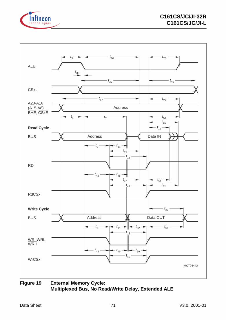
C161CS/JC/JI-32RC161CS/JC/JI-L
Figure 19 External Memory Cycle:Multiplexed Bus, No Read/Write Delay, Extended ALE
Address
Address
Data OUTAddress
Data IN
MCT04442
A23-A16(A15-A8)BHE, CSxE
ALE
CSxL
BUS
RD
RdCSx
Read Cycle
BUS
Write Cycle
t5 t16 t25
t38
t39 t40
t27t17
t7t19
t54
t18
t9 t11
t43
t52
t51
t49
t23
t9
t15
t47
t22 t56
WR, WRL,WRH
WrCSx
t43
t49
t50
t6
t13
t45
t13
t11
t45
Data Sheet 71 V3.0, 2001-01

C161CS/JC/JI-32RC161CS/JC/JI-L
AC Characteristics
Demultiplexed Bus(Operating Conditions apply)ALE cycle time = 4 TCL + 2tA + tC + tF (80 ns at 25 MHz CPU clock without waitstates)
Parameter Symbol Max. CPU Clock= 25 MHz
Variable CPU Clock1 / 2TCL = 1 to 25 MHz
Unit
min. max. min. max.
ALE high time t5 CC 10 + tA – TCL - 10+ tA
– ns
Address setup to ALE t6 CC 4 + tA – TCL - 16+ tA
– ns
ALE falling edge to RD, WR (with RW-delay)
t8 CC 10 + tA – TCL - 10+ tA
– ns
ALE falling edge to RD, WR (no RW-delay)
t9 CC -10 + tA – -10+ tA
– ns
RD, WR low time (with RW-delay)
t12 CC 30 + tC – 2TCL - 10+ tC
– ns
RD, WR low time (no RW-delay)
t13 CC 50 + tC – 3TCL - 10+ tC
– ns
RD to valid data in (with RW-delay)
t14 SR – 20 + tC – 2TCL - 20+ tC
ns
RD to valid data in (no RW-delay)
t15 SR – 40 + tC – 3TCL - 20+ tC
ns
ALE low to valid data in t16 SR – 40 +tA + tC
– 3TCL - 20+ tA + tC
ns
Address to valid data in t17 SR – 50 +2tA + tC
– 4TCL - 30+ 2tA + tC
ns
Data hold after RDrising edge
t18 SR 0 – 0 – ns
Data float after RD rising edge (with RW-delay1))
t20 SR – 26 +2tA + tF
1)– 2TCL - 14
+ 22tA+ tF
1)
ns
Data float after RD rising edge (no RW-delay1))
t21 SR – 10 +2tA + tF
1)– TCL - 10
+ 22tA+ tF
1)
ns
Data Sheet 72 V3.0, 2001-01

C161CS/JC/JI-32RC161CS/JC/JI-L
Data valid to WR t22 CC 20 + tC – 2TCL - 20+ tC
– ns
Data hold after WR t24 CC 10 + tF – TCL - 10+ tF
– ns
ALE rising edge after RD, WR
t26 CC -10 + tF – -10 + tF – ns
Address hold after WR2) t28 CC 0 + tF – 0 + tF – ns
ALE falling edge to CS3) t38 CC -4 - tA 10 - tA -4 - tA 10 - tA ns
CS low to Valid Data In3) t39 SR – 40 +tC + 2tA
– 3TCL - 20+ tC + 2tA
ns
CS hold after RD, WR3) t41 CC 6 + tF – TCL - 14+ tF
– ns
ALE falling edge to RdCS, WrCS (with RW-delay)
t42 CC 16 + tA – TCL - 4+ tA
– ns
ALE falling edge to RdCS, WrCS (no RW-delay)
t43 CC -4 + tA – -4+ tA
– ns
RdCS to Valid Data In(with RW-delay)
t46 SR – 16 + tC – 2TCL - 24+ tC
ns
RdCS to Valid Data In(no RW-delay)
t47 SR – 36 + tC – 3TCL - 24+ tC
ns
RdCS, WrCS Low Time(with RW-delay)
t48 CC 30 + tC – 2TCL - 10+ tC
– ns
RdCS, WrCS Low Time(no RW-delay)
t49 CC 50 + tC – 3TCL - 10+ tC
– ns
Data valid to WrCS t50 CC 26 + tC – 2TCL - 14+ tC
– ns
Data hold after RdCS t51 SR 0 – 0 – ns
Data float after RdCS(with RW-delay)1)
t53 SR – 20 + tF – 2TCL - 20+ 2tA + tF
1)ns
Demultiplexed Bus (cont’d)(Operating Conditions apply)ALE cycle time = 4 TCL + 2tA + tC + tF (80 ns at 25 MHz CPU clock without waitstates)
Parameter Symbol Max. CPU Clock= 25 MHz
Variable CPU Clock1 / 2TCL = 1 to 25 MHz
Unit
min. max. min. max.
Data Sheet 73 V3.0, 2001-01

C161CS/JC/JI-32RC161CS/JC/JI-L
Data float after RdCS(no RW-delay)1)
t68 SR – 0 + tF – TCL - 20+ 2tA + tF
1)ns
Address hold afterRdCS, WrCS
t55 CC -6 + tF – -6 + tF – ns
Data hold after WrCS t57 CC 6 + tF – TCL - 14 + tF
– ns
1) RW-delay and tA refer to the next following bus cycle (including an access to an on-chip X-Peripheral).2) Read data are latched with the same clock edge that triggers the address change and the rising RD edge.
Therefore address changes before the end of RD have no impact on read cycles.3) These parameters refer to the latched chip select signals (CSxL). The early chip select signals (CSxE) are
specified together with the address and signal BHE (see figures below).
Demultiplexed Bus (cont’d)(Operating Conditions apply)ALE cycle time = 4 TCL + 2tA + tC + tF (80 ns at 25 MHz CPU clock without waitstates)
Parameter Symbol Max. CPU Clock= 25 MHz
Variable CPU Clock1 / 2TCL = 1 to 25 MHz
Unit
min. max. min. max.
Data Sheet 74 V3.0, 2001-01

C161CS/JC/JI-32RC161CS/JC/JI-L
Figure 20 External Memory Cycle:Demultiplexed Bus, With Read/Write Delay, Normal ALE
Data OUT
Address
Data IN
MCT04443
A23-A16A15-A0BHE, CSxE
ALE
CSxL
RD
RdCSx
Read Cycle
Write Cycle
t5 t16 t26
t38 t39 t41
t28t17
t6t20
t55
t18
t8t12
t42
t53
t51
t48
t24
t8
t14
t46
t22 t57
WR, WRL,WRH
WrCSx
t12
t42
t48
t50
BUS(D15-D8)D7-D0
BUS(D15-D8)D7-D0
Data Sheet 75 V3.0, 2001-01
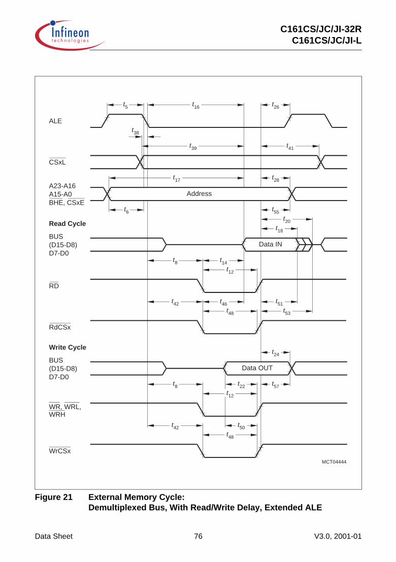
C161CS/JC/JI-32RC161CS/JC/JI-L
Figure 21 External Memory Cycle:Demultiplexed Bus, With Read/Write Delay, Extended ALE
Address
Data OUT
Data IN
MCT04444
A23-A16A15-A0BHE, CSxE
ALE
CSxL
RD
RdCSx
Read Cycle
Write Cycle
t5 t16 t26
t38
t39 t41
t28t17
t20
t55
t18
t8t12
t42
t53
t51
t48
t24
t8
t14
t46
t22 t57
WR, WRL,WRH
WrCSx
t12
t42
t48
t50
t6
BUS(D15-D8)D7-D0
BUS(D15-D8)D7-D0
Data Sheet 76 V3.0, 2001-01

C161CS/JC/JI-32RC161CS/JC/JI-L
Figure 22 External Memory Cycle:Demultiplexed Bus, No Read/Write Delay, Normal ALE
Data OUT
Address
Data IN
MCT04445
A23-A16A15-A0BHE, CSxE
ALE
CSxL
RD
RdCSx
Read Cycle
Write Cycle
t5 t16 t26
t38 t39 t41
t28t17
t6t21
t55
t18
t9t13
t43
t68
t51
t49
t24
t15
t47
t22 t57
WR, WRL,WRH
WrCSx
t13
t43
t49
t50
BUS(D15-D8)D7-D0
BUS(D15-D8)D7-D0
t9
Data Sheet 77 V3.0, 2001-01

C161CS/JC/JI-32RC161CS/JC/JI-L
Figure 23 External Memory Cycle:Demultiplexed Bus, No Read/Write Delay, Extended ALE
Address
Data OUT
Data IN
MCT04446
A23-A16A15-A0BHE, CSxE
ALE
CSxL
RD
RdCSx
Read Cycle
Write Cycle
t5 t16 t26
t38
t39 t41
t28t17
t21
t55
t18
t9t13
t43
t68
t51
t49
t24
t9
t15
t47
t22 t57
WR, WRL,WRH
WrCSx
t13
t43
t49
t50
t6
BUS(D15-D8)D7-D0
BUS(D15-D8)D7-D0
Data Sheet 78 V3.0, 2001-01

C161CS/JC/JI-32RC161CS/JC/JI-L
AC Characteristics
CLKOUT and READY(Operating Conditions apply)
Parameter Symbol Max. CPU Clock= 25 MHz
Variable CPU Clock1 / 2TCL = 1 to 25 MHz
Unit
min. max. min. max.
CLKOUT cycle time t29 CC 40 40 2TCL 2TCL ns
CLKOUT high time t30 CC 14 – TCL - 6 – ns
CLKOUT low time t31 CC 10 – TCL - 10 – ns
CLKOUT rise time t32 CC – 4 – 4 ns
CLKOUT fall time t33 CC – 4 – 4 ns
CLKOUT rising edge to ALE falling edge
t34 CC 0 + tA 10 + tA 0 + tA 10 + tA ns
Synchronous READYsetup time to CLKOUT
t35 SR 14 – 14 – ns
Synchronous READYhold time after CLKOUT
t36 SR 4 – 4 – ns
Asynchronous READYlow time
t37 SR 54 – 2TCL + t58 – ns
Asynchronous READYsetup time1)
1) These timings are given for test purposes only, in order to assure recognition at a specific clock edge.
t58 SR 14 – 14 – ns
Asynchronous READYhold time1)
t59 SR 4 – 4 – ns
Async. READY hold time after RD, WR high (Demultiplexed Bus)2)
2) Demultiplexed bus is the worst case. For multiplexed bus 2TCL are to be added to the maximum values. Thisadds even more time for deactivating READY.The 2tA and tC refer to the next following bus cycle, tF refers to the current bus cycle.The maximum limit for t60 must be fulfilled if the next following bus cycle is READY controlled.
t60 SR 0 0+ 2tA + tC + tF
2)
0 TCL - 20+ 2tA + tC + tF
2)
ns
Data Sheet 79 V3.0, 2001-01

C161CS/JC/JI-32RC161CS/JC/JI-L
Figure 24 CLKOUT and READY
Notes1) Cycle as programmed, including MCTC waitstates (Example shows 0 MCTC WS).2) The leading edge of the respective command depends on RW-delay.3) READY sampled HIGH at this sampling point generates a READY controlled waitstate,
READY sampled LOW at this sampling point terminates the currently running bus cycle.4) READY may be deactivated in response to the trailing (rising) edge of the corresponding command (RD or
WR).5) If the Asynchronous READY signal does not fulfill the indicated setup and hold times with respect to CLKOUT
(e.g. because CLKOUT is not enabled), it must fulfill t37 in order to be safely synchronized. This is guaranteed,if READY is removed in reponse to the command (see Note4)).
6) Multiplexed bus modes have a MUX waitstate added after a bus cycle, and an additional MTTC waitstate maybe inserted here.For a multiplexed bus with MTTC waitstate this delay is 2 CLKOUT cycles, for a demultiplexed bus withoutMTTC waitstate this delay is zero.
7) The next external bus cycle may start here.
MCT04447
t32
CLKOUT
ALE
CommandRD, WR
SyncREADY
AsyncREADY
t33
t29t30
t31
t34
7)
2)
3)3)
t35
t36
t35
t36
t58
t59
3)
t58
t59
3)
t37 5)
t60 4)
see 6)
Running Cycle 1)READY
Waitstate MUX/Tristate 6)
Data Sheet 80 V3.0, 2001-01

C161CS/JC/JI-32RC161CS/JC/JI-L
AC Characteristics
External Bus Arbitration(Operating Conditions apply)
Parameter Symbol Max. CPU Clock= 25 MHz
Variable CPU Clock1 / 2TCL = 1 to 25 MHz
Unit
min. max. min. max.
HOLD input setup timeto CLKOUT
t61 SR 20 – 20 – ns
CLKOUT to HLDA highor BREQ low delay
t62 CC – 20 – 20 ns
CLKOUT to HLDA lowor BREQ high delay
t63 CC – 20 – 20 ns
CSx release t64 CC – 20 – 20 ns
CSx drive t65 CC -4 24 -4 24 ns
Other signals release t66 CC – 20 – 20 ns
Other signals drive t67 CC – 4 24 – 4 24 ns
Data Sheet 81 V3.0, 2001-01

C161CS/JC/JI-32RC161CS/JC/JI-L
Figure 25 External Bus Arbitration, Releasing the Bus
Notes1) The C161CS/JC/JI will complete the currently running bus cycle before granting bus access.2) This is the first possibility for BREQ to get active.3) The CS outputs will be resistive high (pullup) after t64.
MCT04448
t61
t62
CLKOUT
HOLD
HLDA
BREQ
CSx(On P6.x)
OtherSignals
t63
t64
t66
see1)
3)
1)
2)
Data Sheet 82 V3.0, 2001-01

C161CS/JC/JI-32RC161CS/JC/JI-L
Figure 26 External Bus Arbitration, (Regaining the Bus)
Notes1) This is the last chance for BREQ to trigger the indicated regain-sequence.
Even if BREQ is activated earlier, the regain-sequence is initiated by HOLD going high.Please note that HOLD may also be deactivated without the C161CS/JC/JI requesting the bus.
2) The next C161CS/JC/JI driven bus cycle may start here.
MCT04449
t61
t62
t62 t62 t63
t65
t67
CLKOUT
HOLD
HLDA
BREQ
CSx(On P6.x)
OtherSignals
2)
1)
Data Sheet 83 V3.0, 2001-01
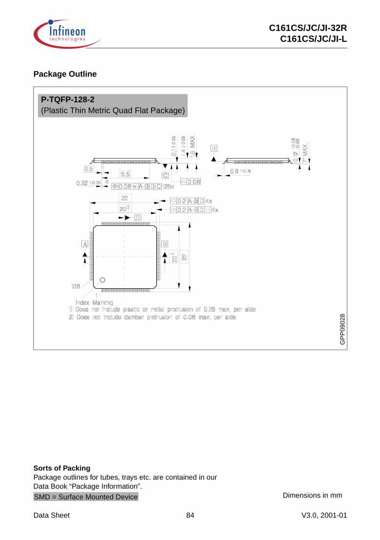
C161CS/JC/JI-32RC161CS/JC/JI-L
Package Outline
P-TQFP-128-2(Plastic Thin Metric Quad Flat Package)
GP
P09
028
Sorts of PackingPackage outlines for tubes, trays etc. are contained in ourData Book “Package Information”.
Dimensions in mmSMD = Surface Mounted Device
Data Sheet 84 V3.0, 2001-01

h t t p : / / w w w . i n f i n e o n . c o m
Published by Infineon Technologies AG
Infineon goes for Business Excellence
“Business excellence means intelligent approaches and clearly defined processes, which are both constantly under review and ultimately lead to good operating results.Better operating results and business excellence mean less idleness and wastefulness for all of us, more professional success, more accurate information, a better overview and, thereby, less frustration and more satisfaction.”
Dr. Ulrich Schumacher