Embed Size (px)
Citation preview

1
®®Southwest Test Workshop 2000
Grace Chan / Justin LeungJune 12th, 2000
C4 Probe Card Space Transformer Technology
Overview
Grace ChanJustin Leung
Intel Corporation

2
®®Southwest Test Workshop 2000
Grace Chan / Justin LeungJune 12th, 2000
Outline
! C4 Probe Card Space Transformer Overview
! Multi-layer Ceramic Space Transformers ! Future Space Transformer Technologies

3
®®Southwest Test Workshop 2000
Grace Chan / Justin LeungJune 12th, 2000
C4 Probe Card Cross-section
PCB
ST
interposer (BGA, PGA, etc..)
decoupling caps
decoupling caps
pogos
3 Major Components of a Probe Card
C4 Probes
4
®®Southwest Test Workshop 2000
Grace Chan / Justin LeungJune 12th, 2000
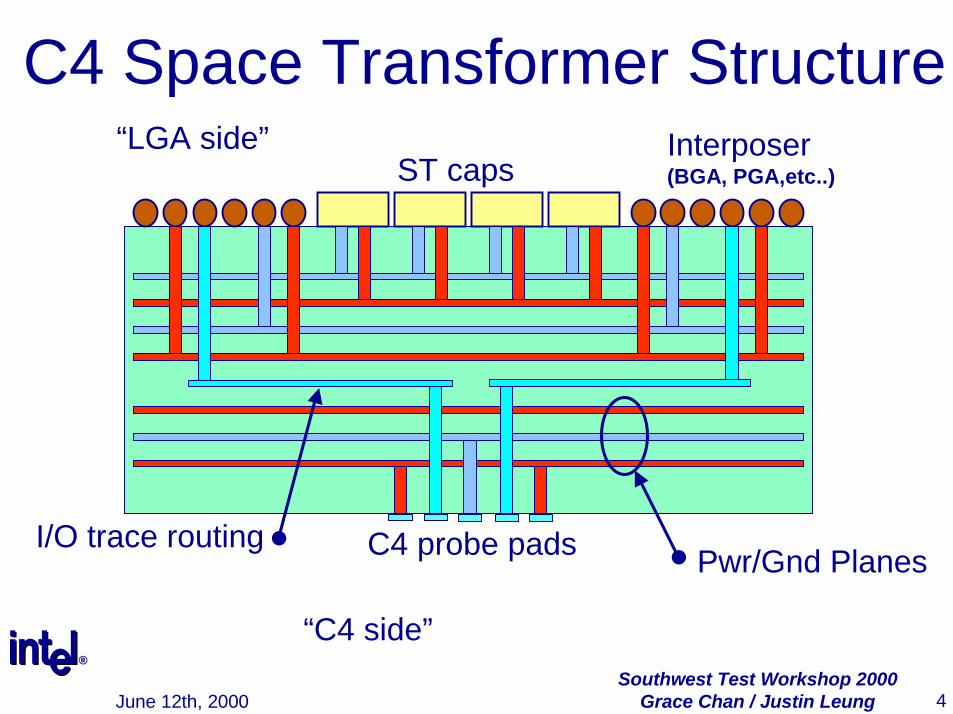
C4 Space Transformer Structure“LGA side”
“C4 side”
I/O trace routing
ST capsInterposer(BGA, PGA,etc..)
Pwr/Gnd PlanesC4 probe pads
5
®®Southwest Test Workshop 2000
Grace Chan / Justin LeungJune 12th, 2000
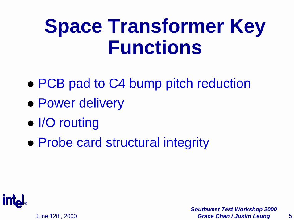
Space Transformer Key Functions
! PCB pad to C4 bump pitch reduction! Power delivery ! I/O routing! Probe card structural integrity

6
®®Southwest Test Workshop 2000
Grace Chan / Justin LeungJune 12th, 2000
YEAR 1999 2000 2001 2002 2003 2004 2005TECHNOLOGY NODE 180 nm 130 nm 100nm
C4 Area Array bump pitch (µm) 200 200 200 200 200 200 150
Chip size (mm2) 450 450 450 509 567 595 622
Projected bump count 11250 11250 11250 12725 14175 14875 27644
Clock Frequency (MHz) 1200 1321 1454 1600 1724 1857 2000
Power (W) 90 100 115 130 140 150 160
Core Supply Voltage (V) 1.8 1.8 1.8 1.5 1.5 1.2 1.2
Maximum Current (A) 50 56 64 87 93 125 133
Microprocessor Performance Trends
Data abstracted from International TechnologyRoadmap for Semiconductors, 1999 Edition

7
®®Southwest Test Workshop 2000
Grace Chan / Justin LeungJune 12th, 2000
Space Transformer Critical Physical Parameters Minimum Via Diameter and PitchMinimum Line and Space DimensionsDielectric Thickness (100 - 250 µm)Relative Dielectric Permittivity (εr = 3.0 - 9.5)Metal Sheet Resistance (3 - 10 mΩ/sq)Power/Ground Perforation (0 - 50%)Coefficient of Thermal Expansion (3 to 70 ppm/oC)Flexural Strength (80 - 400 MPa)Thermal Conductivity (0.2 - 200 W/m-K)
8
®®Southwest Test Workshop 2000
Grace Chan / Justin LeungJune 12th, 2000
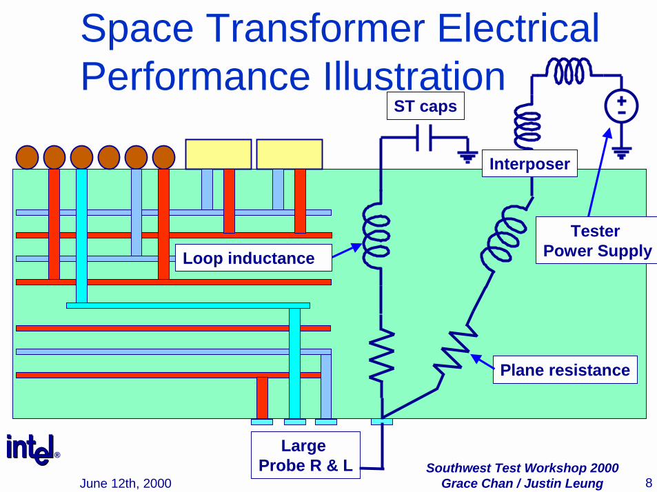
Space Transformer ElectricalPerformance Illustration
ST caps
Interposer
Tester Power SupplyLoop inductance
Plane resistance
Large Probe R & L

9
®®Southwest Test Workshop 2000
Grace Chan / Justin LeungJune 12th, 2000
Package and Space Transformer Comparison
Package Space Transformer
I/O Route all traces Only route subset of I/O's
PWR/GND All bumps Probe subset of bumps
Number of layers Cost restriction Minimize via inductance
On-Pkg Capacitors Cost restriction Maximize # Caps
Force Insertion Probe forces
Operating Temperature
Designed for external temperature compatibility Designed for sort
Reliability Thermal shock tests Mechanical touchdowns
Connections C4 bumps C4 probes (high R & L)
10
®®Southwest Test Workshop 2000
Grace Chan / Justin LeungJune 12th, 2000
Space Transformer -Multi-layer Ceramic
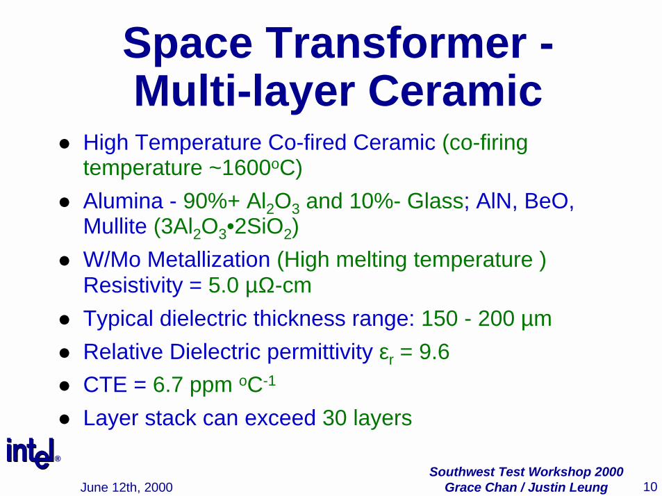
! High Temperature Co-fired Ceramic (co-firing temperature ~1600oC)
! Alumina - 90%+ Al2O3 and 10%- Glass; AlN, BeO, Mullite (3Al2O3•2SiO2)
! W/Mo Metallization (High melting temperature )Resistivity = 5.0 µΩ-cm
! Typical dielectric thickness range: 150 - 200 µm! Relative Dielectric permittivity εr = 9.6! CTE = 6.7 ppm oC-1
! Layer stack can exceed 30 layers
11
®®Southwest Test Workshop 2000
Grace Chan / Justin LeungJune 12th, 2000
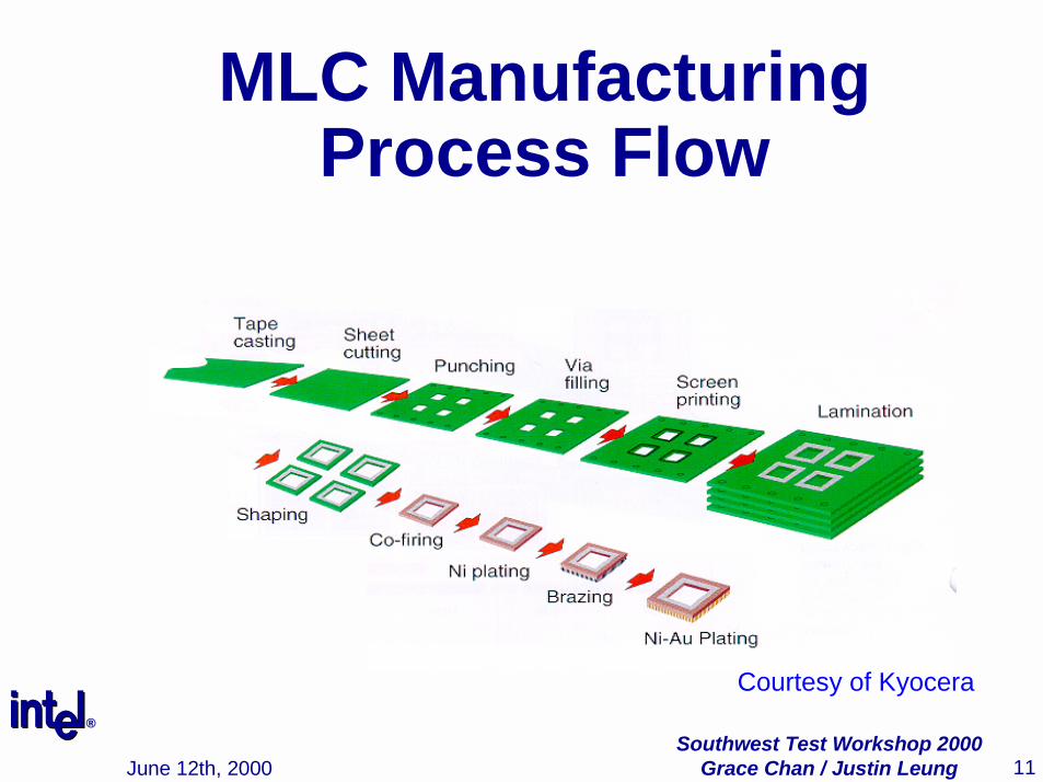
MLC Manufacturing Process Flow
Courtesy of Kyocera

12
®®Southwest Test Workshop 2000
Grace Chan / Justin LeungJune 12th, 2000
Multi-layer Ceramic Cross-Section
Courtesy of NTK
13
®®Southwest Test Workshop 2000
Grace Chan / Justin LeungJune 12th, 2000
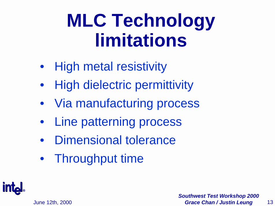
MLC Technology limitations
• High metal resistivity• High dielectric permittivity• Via manufacturing process• Line patterning process• Dimensional tolerance• Throughput time

14
®®Southwest Test Workshop 2000
Grace Chan / Justin LeungJune 12th, 2000
Future Space Transformer Technologies
! MLC with Multiple-layer Thin Film (MLC-MTF)
! AlN Substrate with Multiple-layer Thin Film
! Organic Build-up! Glass Ceramic

15
®®Southwest Test Workshop 2000
Grace Chan / Justin LeungJune 12th, 2000
MLC with Multi-layer Thin Film
! Thin-film build-up occurs after co-firing process
! Polyimide (PI) thin film build-up on Al2O3 Ceramic by spin coating
! Cu metallization on PI thin film by photopatterning
! Fine line width and via dimensions

16
®®Southwest Test Workshop 2000
Grace Chan / Justin LeungJune 12th, 2000
MLC-MTF Illustration
Courtesy of NTK
17
®®Southwest Test Workshop 2000
Grace Chan / Justin LeungJune 12th, 2000
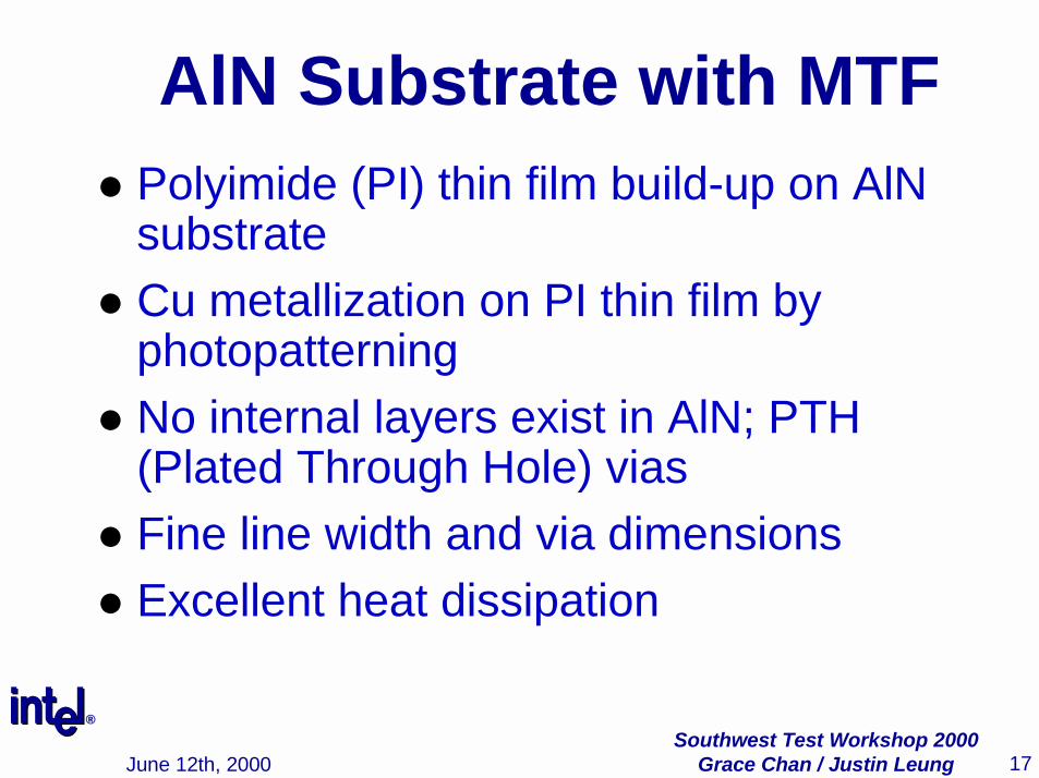
AlN Substrate with MTF ! Polyimide (PI) thin film build-up on AlN
substrate! Cu metallization on PI thin film by
photopatterning! No internal layers exist in AlN; PTH
(Plated Through Hole) vias ! Fine line width and via dimensions! Excellent heat dissipation

18
®®Southwest Test Workshop 2000
Grace Chan / Justin LeungJune 12th, 2000
AlN with MTF Illustration
Al-Nw/ PTH

19
®®Southwest Test Workshop 2000
Grace Chan / Justin LeungJune 12th, 2000
Organic Build-up Solution! Organic build-up on both sides of a core! Cu metallization; line pattern defined by
photopatterning! Via formation by laser drilling or
photolithography at build-up; PTH through core
! Fine line width and via dimensions

20
®®Southwest Test Workshop 2000
Grace Chan / Justin LeungJune 12th, 2000
Organic Build-up Illustration
Courtesy of NTK
21
®®Southwest Test Workshop 2000
Grace Chan / Justin LeungJune 12th, 2000
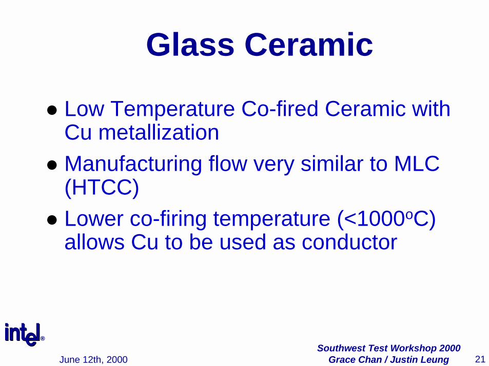
Glass Ceramic
! Low Temperature Co-fired Ceramic with Cu metallization
! Manufacturing flow very similar to MLC (HTCC)
! Lower co-firing temperature (<1000oC) allows Cu to be used as conductor

22
®®Southwest Test Workshop 2000
Grace Chan / Justin LeungJune 12th, 2000
Glass Ceramic Illustration
Courtesy of NTK

23
®®Southwest Test Workshop 2000
Grace Chan / Justin LeungJune 12th, 2000
Technology ComparisonMLC-MTF AlN-MTF Organic Build-up Glass Ceramic
W/Mo; Cu for TF W in PTH; Cu for TF Cu Cu
9.2-9.6 8.8 3.6 5.3
Fair Poor Fair Good
Good Good Good Fair
Fair Fair Poor Good
Good Excellent Poor Fair
Fair Fair Poor Good
Poor Fair Good FairThroughput Time
Conductor
CTE mismatch with PCB
Dielectric Constant
Power Delivery
Structural Integrity
Thermal Conductivity
Routing Capability

24
®®Southwest Test Workshop 2000
Grace Chan / Justin LeungJune 12th, 2000
Summary! A space transformer is a major component of a probe
card. It provides pitch reduction, high routing density and localized mid-frequency decoupling.
! A space transformer and a microprocessor package have very different design driving factors. An optimal package design may not be a good space transformer.
! With accelerating microprocessor performance, future space transformer technologies are necessary. MLC-MTF, AlN-MTF, Organic build-up, and glass ceramic are all contenders to be the next generation technology.