Embed Size (px)
Citation preview

C7X99-OCEC7X99-OCE-F
USER’S MANUAL
Revision 1.1
The information in this User’s Manual has been carefully reviewed and is believed to be accurate. The vendor assumes no responsibility for any inaccuracies that may be contained in this document, makes no commitment to update or to keep current the information in this manual, or to notify any person or organization of the updates. Please Note: For the most up-to-date version of this manual, please see our web site at www.supermicro.com.
Super Micro Computer, Inc. ("Supermicro") reserves the right to make changes to the product de-scribed in this manual at any time and without notice. This product, including software and documenta-tion, is the property of Supermicro and/or its licensors, and is supplied only under a license. Any use or reproduction of this product is not allowed, except as expressly permitted by the terms of said license.
IN NO EVENT WILL SUPERMICRO BE LIABLE FOR DIRECT, INDIRECT, SPECIAL, INCIDEN-TAL, SPECULATIVE OR CONSEQUENTIAL DAMAGES ARISING FROM THE USE OR INABILITY TO USE THIS PRODUCT OR DOCUMENTATION, EVEN IF ADVISED OF THE POSSIBILITY OF SUCH DAMAGES. IN PARTICULAR, SUPERMICRO SHALL NOT HAVE LIABILITY FOR ANY HARDWARE, SOFTWARE, OR DATA STORED OR USED WITH THE PRODUCT, INCLUDING THE COSTS OF REPAIRING, REPLACING, INTEGRATING, INSTALLING OR RECOVERING SUCH HARDWARE, SOFTWARE, OR DATA.
Any disputes arising between manufacturer and customer shall be governed by the laws of Santa Clara County in the State of California, USA. The State of California, County of Santa Clara shall be the exclusive venue for the resolution of any such disputes. Super Micro's total liability for all claims will not exceed the price paid for the hardware product.
FCC Statement: This equipment has been tested and found to comply with the limits for a class B digital device, pursuant to Part 15 of the FCC Rules. These limits are designed to provide reasonable protection against harmful interference in a residential installation. This equipment generates, uses, and can radiate radio frequency energy and, if not installed and used in accordance with the instruc-tions, may cause harmful interference to radio communications. However, there is no guarantee that interference will not occur in a particular installation. If this equipment does cause harmful interfer-ence to radio or television reception, which can be determined by turning the equipment off and on, the user is encouraged to try to correct the interference by one or more of the following measures:
• Reorient or relocate the receiving antenna. • Increase the separation between the equipment and receiver. • Connect the equipment to an outlet on a circuit different from that to which the receiver is connected. • Consult the authorized dealer or an experienced radio/TV technician for help.
California Best Management Practices Regulations for Perchlorate Materials: This Perchlorate warning applies only to products containing CR (Manganese Dioxide) Lithium coin cells. “Perchlorate Material-special handling may apply. See www.dtsc.ca.gov/hazardouswaste/perchlorate”
WARNING: Handling of lead solder materials used in this product may expose you to lead, a chemi-cal known to the State of California to cause birth defects and other reproductive harm.
Manual Revision 1.1 Release Date: September 21, 2016
Unless you request and receive written permission from Super Micro Computer, Inc., you may not copy any part of this document.
Information in this document is subject to change without notice. Other products and companies referred to herein are trademarks or registered trademarks of their respective companies or mark holders.
Copyright © 2016 by Super Micro Computer, Inc. All rights reserved. Printed in the United States of America

iii
Preface
This manual is written for system integrators, PC technicians and knowledgeable PC users. It provides information for the installation and use of the C7X99-OCE/C7X99-OCE-F motherboard.
Manual Organization
Chapter 1 describes the features, specifications and performance of the motherboard, and provides detailed information on the Intel X99 Express chipset.
Chapter 2 provides hardware installation instructions. Read this chap-ter when installing the processor, memory modules and other hardware components into the system.
If you encounter any problems, see Chapter 3, which describes trouble-shooting procedures for video, memory and system setup stored in the CMOS.
Chapter 4 includes an introduction to the BIOS, and provides detailed information on running the CMOS Setup utility.
Appendix A provides BIOS Error Beep Codes.
Appendix B lists software program installation instructions.
Appendix C contains UEFI BIOS Recovery instructions.
Appendix D contains an introduction and instructions regarding the Dual Boot Block feature of this motherboard.
Preface
iv
Conventions Used in the Manual
Special attention should be given to the following symbols for proper installation and to prevent damage done to the components or injury to yourself:
Attention! Critical information to prevent damage to the com-ponents or injury to yourself.
Important: Important information given to ensure proper sys-tem installation or to relay safety precautions.
Note: Additional Information given to differentiate various mod-els or provides information for correct system setup.
Supermicro C7X99-OCE/C7X99-OCE-F Motherboard User’s Manual
Checklist
Congratulations on purchasing your computer motherboard from an ac-knowledged leader in the industry. Supermicro boards are designed with the utmost attention to detail to provide you with the highest standards in quality and performance.
Please check that the following items have all been included with your motherboard. If anything listed here is damaged or missing, contact your retailer.
The following items are included in the retail box.
• One (1) Supermicro Motherboard
• Six (6) SATA cables (single packed/boxed only) or,
• Two (2) SATA cables (bulk packed only)
• One (1) I/O shield
• One (1) Quick Reference Guide
• One (1) Driver CD (C7X99-OCE single packed/boxed only)
v
Standardized Warning Statements
Standardized Warning Statements
The following statements are industry-standard warnings, provided to warn the user of situations which have the potential for bodily injury. Should you have questions or experience difficulty, contact Supermicro's Technical Support department for assistance. Only certified technicians should attempt to install or configure components.
Read this section in its entirety before installing or configuring compo-nents in the Supermicro chassis.
Battery Handling
Warnung
Bei Einsetzen einer falschen Batterie besteht Explosionsgefahr. Ersetzen Sie die Batterie nur durch den gleichen oder vom Hersteller empfohlenen Batterietyp. Entsorgen Sie die benutzten Batterien nach den Anweisungen des Herstellers.
Warning!
There is a danger of explosion if the battery is replaced incorrectly. Re-place the battery only with the same or equivalent type recommended by the manufacturer. Dispose of used batteries according to the manu-facturer's instructions
電池の取り扱い
電池交換が正しく行われなかった場合、破裂の危険性があります。 交換する電池はメーカーが推奨する型、または同等のものを使用下さい。 使用済電池は製造元の指示に従って処分して下さい。
警告
电池更换不当会有爆炸危险。请只使用同类电池或制造商推荐的功能相当的电池更
换原有电池。请按制造商的说明处理废旧电池。
警告
電池更換不當會有爆炸危險。請使用製造商建議之相同或功能相當的電池更換原有
電池。請按照製造商的說明指示處理廢棄舊電池。
Attention
Danger d'explosion si la pile n'est pas remplacée correctement. Ne la remplacer que par une pile de type semblable ou équivalent, recom-mandée par le fabricant. Jeter les piles usagées conformément aux instructions du fabricant.

vi
¡Advertencia!
Existe peligro de explosión si la batería se reemplaza de manera incor-recta. Reemplazar la batería exclusivamente con el mismo tipo o el equivalente recomendado por el fabricante. Desechar las baterías gasta-das según las instrucciones del fabricante.
Supermicro C7X99-OCE/C7X99-OCE-F Motherboard User’s Manual
אזהרה!יש להחליף של הסוללה במידה והוחלפה בדרך לא תקינה. פיצוץקיימת סכנת
.צתיצרן מומלחברת התואם מ את הסוללה בסוג
לפי הוראות היצרן. יש לבצע המשומשות סילוק הסוללות
فعليل بطريقة غير صحيحة البطارية انفجار في حالة اسحبذال من هناك خطر اسحبذال البطارية
به الشرمة المصنعة أوصثمما أو ما يعادلها بنفس النىع فقط حعليمات الشرمة الصانعةالمسحعملة وفقا ل جخلص من البطاريات
경고!
배터리가 올바르게 교체되지 않으면 폭발의 위험이 있습니다. 기존 배터리와 동일
하거나 제조사에서 권장하는 동등한 종류의 배터리로만 교체해야 합니다. 제조사
의 안내에 따라 사용된 배터리를 처리하여 주십시오.
Waarschuwing
Er is ontploffingsgevaar indien de batterij verkeerd vervangen wordt. Ver-vang de batterij slechts met hetzelfde of een equivalent type die door de fabrikant aanbevolen wordt. Gebruikte batterijen dienen overeenkomstig fabrieksvoorschriften afgevoerd te worden.
Product Disposal
Warning! Ultimate disposal of this product should be handled according to all na-tional laws and regulations.

vii
Standardized Warning Statements
製品の廃棄
この製品を廃棄処分する場合、国の関係する全ての法律・条例に従い処理する必要があります。
警告
本产品的废弃处理应根据所有国家的法律和规章进行。
警告
本產品的廢棄處理應根據所有國家的法律和規章進行。
Warnung
Die Entsorgung dieses Produkts sollte gemäß allen Bestimmungen und Gesetzen des Landes erfolgen.
¡Advertencia!
Al deshacerse por completo de este producto debe seguir todas las leyes y reglamentos nacionales.
Attention
La mise au rebut ou le recyclage de ce produit sont généralement soumis à des lois et/ou directives de respect de l'environnement. Renseignez-vous auprès de l'organisme compétent.
סילוק המוצר
אזהרה!
חוקי המדינה.סילוק סופי של מוצר זה חייב להיות בהתאם להנחיות ו
Waarschuwing
De uiteindelijke verwijdering van dit product dient te geschieden in over-eenstemming met alle nationale wetten en reglementen.
القىانين واللىائح الىطنيةجميع وفقا ل ينبغي التعامل معه هذا المنتج من التخلص النهائي عند
경고!
이 제품은 해당 국가의 관련 법규 및 규정에 따라 폐기되어야 합니다.

viii
Supermicro C7X99-OCE/C7X99-OCE-F Motherboard User’s Manual
Contacting Supermicro
Headquarters
Address: Super Micro Computer, Inc.
980 Rock Ave.
San Jose, CA 95131 U.S.A.
Tel: +1 (408) 503-8000
Fax: +1 (408) 503-8008
Email: [email protected] (General Information)
[email protected] (Technical Support)
Web Site:
www.supermicro.com
Europe
Address: Super Micro Computer B.V.
Het Sterrenbeeld 28, 5215 ML
's-Hertogenbosch, The Netherlands
Tel: +31 (0) 73-6400390
Fax: +31 (0) 73-6416525
Email: [email protected] (General Information)
[email protected] (Technical Support)
[email protected] (Customer Support)
Asia-Pacific
Address: Super Micro Computer, Inc.
4F, No. 232-1, Liancheng Rd
Chung-Ho Dist., New Taipei City 235
Taiwan
Tel: +886-(2) 8226-3990
Fax: +886-(2) 8226-3991
Web Site:
www.supermicro.com.tw
Technical Support:
Email: [email protected]
Tel: +886-(2)-8226-3990

ix
Contacting Supermicro
Where to Find More Information
For your system to work properly, please follow the links below to download all necessary drivers/utilities and the user's manual for your motherboard.
SMCI product manuals: http://www.supermicro.com/support/manuals/
Product Drivers and utilities: ftp://ftp.supermicro.com/
If you have any questions, please contact our support team at [email protected].
x
Table of Contents
Preface
Manual Organization ..........................................................................iiiChecklist ..........................................................................................ivConventions Used in the Manual .........................................................ivStandardized Warning Statements ....................................................... v
Battery Handling ....................................................................... vProduct Disposal .......................................................................vi
Contacting Supermicro ..................................................................... viiiWhere to Find More Information..........................................................ix
Chapter 1 Introduction
1-1 Overview .............................................................................. 1-1About this Motherboard .......................................................... 1-1
1-2 Chipset Overview .................................................................. 1-1Intel X99 Express Chipset Features .......................................... 1-1
1-3 Motherboard Features ............................................................... 1-21-4 Special Features .................................................................... 1-4
Recovery from AC Power Loss ................................................. 1-41-5 PC Health Monitoring .............................................................. 1-4
Fan Status Monitor with Firmware Control ............................... 1-4Environmental Temperature Control ......................................... 1-4System Resource Alert ........................................................... 1-5
1-6 ACPI Features ....................................................................... 1-5Slow Blinking LED for Suspend-State Indicator .......................... 1-5
1-7 Power Supply ........................................................................ 1-61-8 Super I/O ............................................................................. 1-6
Chapter 2 Installation
2-1 Installation Components and Tools Needed ............................... 2-12-2 Static-Sensitive Devices .......................................................... 2-2
Precautions ........................................................................... 2-2Unpacking ............................................................................. 2-2
2-3 Processor and Heatsink Installation .......................................... 2-3Installing the Processor ......................................................... 2-3Installing a CPU Heatsink ........................................................ 2-7
Supermicro C7X99-OCE/C7X99-OCE-F Motherboard User’s Manual
xi
Table of Contents
Removing a Heatsink ............................................................. 2-82-4 Installing DDR4 Memory ......................................................... 2-9
DIMM Installation .................................................................. 2-9Removing Memory Modules ..................................................... 2-9Memory Population Guidelines ............................................... 2-10Memory Support .................................................................. 2-10
2-5 Motherboard Installation ....................................................... 2-12Tools Needed ....................................................................... 2-12Location of Mounting Holes ................................................... 2-12Installing the Motherboard .................................................... 2-13
2-6 Connectors/IO Ports ............................................................. 2-14Back I/O Panel .................................................................... 2-14
Universal Serial Bus (USB) ................................................ 2-15Ethernet Ports ................................................................. 2-16Back Panel High Definition Audio (HD Audio) ...................... 2-16PS/2 Keyboard/Mouse Port ................................................ 2-17VGA Port (C7X99-OCE-F only) ........................................... 2-17
Front Control Panel .............................................................. 2-18Front Control Panel Pin Definitions ......................................... 2-19
Power LED ..................................................................... 2-19HDD LED ........................................................................ 2-19NIC1/NIC2 (LAN1/LAN2) ................................................... 2-19Overheat (OH)/Fan Fail ..................................................... 2-19NMI Button ..................................................................... 2-20Power Fail ....................................................................... 2-20Reset Button .................................................................. 2-20Power Button .................................................................. 2-20
2-7 Connecting Cables ............................................................... 2-21ATX Main PWR & CPU PWR Connectors (JPW1 & JPW2) ........ 2-21Fan Headers (Fan 1 ~ Fan 5) ............................................ 2-22Chassis Intrusion (JL1) .................................................... 2-22Internal Buzzer (SP1) ....................................................... 2-23Power LED / Speaker (JD1) ............................................... 2-23DOM PWR Connector (JSD1).............................................. 2-24Standby Power Header (STBY1) ......................................... 2-24
System Management Bus (JIPMB1) ................................2-24TPM Header (JTPM1) ........................................................ 2-25
Power Supply I2C (JPI2C1) ................................................ 2-25Front Panel Audio Header (AUDIO FP) ................................ 2-26
xii
OC Front Panel (OC FRONT PANEL) .................................... 2-262-8 Jumper Settings .................................................................. 2-27
Explanation of Jumpers ........................................................ 2-27LAN1/LAN2 Enable/Disable ................................................ 2-27Clear CMOS (JBT1, CLR_CMOS_SW) ................................... 2-28
PCI Slot SMB Enable (I2C1/I2C2) ........................................ 2-28Audio Enable (JPAC1) ....................................................... 2-29Watch Dog Enable/Disable ................................................. 2-29USB Wake-Up (JPUSB1) .................................................... 2-30Over-Clock Management Buttons ....................................... 2-31Manufacturing Mode (JPME2) ............................................. 2-32VGA Enable/Disable (JPG1) ............................................... 2-32BMC Enable/Disable (JPB1) ............................................... 2-32BIOS Recovery Switch (JBR1) ............................................ 2-33Power Button (S4) ........................................................... 2-33BIOS Restore (S11) .......................................................... 2-33
2-9 Onboard Indicators ................................................................ 2-34LAN 1/LAN 2 LEDs ........................................................... 2-34BMC Heartbeat (LEDM1) .................................................. 2-34Power LED (LED1) ........................................................... 2-35Status Display (LED4) ..................................................... 2-35
2-10 SATA Connections ................................................................ 2-36SATA Connections (I-SATA0~5, S-SATA0~3) ........................ 2-36
2-10 The OC Front Control Panel (Optional) ................................... 2-37Over-Clocking Buttons (OC1, OC2, OC3) ............................. 2-37Clear CMOS and Reset ...................................................... 2-37Boot BIOS Switch ............................................................. 2-37BIOS Recovery................................................................. 2-37Front USB Port ................................................................ 2-37Installing the OC Front Control Panel .................................. 2-38
Chapter 3 Troubleshooting
3-1 Troubleshooting Procedures ..................................................... 3-1Before Power On.................................................................... 3-1No Power .............................................................................. 3-1No Video .............................................................................. 3-2Memory Errors ..................................................................... 3-2When the System is Losing the Setup Configuration .................. 3-2
Supermicro C7X99-OCE/C7X99-OCE-F Motherboard User’s Manual
xiii
Table of Contents
3-2 Technical Support Procedures .................................................. 3-33-3 Frequently Asked Questions .................................................... 3-43-4 Battery Removal and Installation ............................................. 3-5
Battery Removal .................................................................... 3-5Proper Battery Disposal .......................................................... 3-5
3-5 Returning Motherboard for Service ........................................... 3-6Battery Installation ................................................................ 3-6
Chapter 4 BIOS
4-1 Introduction .......................................................................... 4-1Starting BIOS GUI Setup Utility ............................................... 4-1How To Change the Configuration Data .................................... 4-2How to Start the Setup Utility ................................................. 4-2
4-2 Saving and Loading................................................................ 4-3Save and Load ...................................................................... 4-3
Restore Defaults ................................................................ 4-4Save All Settings Only ........................................................ 4-4Save Changes and Exit ....................................................... 4-4Save Changes and Reset ..................................................... 4-4Discard Changes ............................................................... 4-4Exit without Save ............................................................... 4-4Discard Changes and Reset ................................................. 4-4
Profiles ................................................................................. 4-44-3 System Information ............................................................... 4-6
Motherboard ......................................................................... 4-6System Date ..................................................................... 4-6System Time ..................................................................... 4-6
CPU ..................................................................................... 4-7Memory ................................................................................ 4-8
4-4 Processor/CPU ....................................................................... 4-9Motherboard ......................................................................... 4-9Performance ........................................................................ 4-10
Hyper-Threading [ALL] ...................................................... 4-10Execute Disable Bit .......................................................... 4-10Intel® Virtualization Technology ........................................ 4-10PPIN Control .................................................................... 4-11Hardware Prefetcher ......................................................... 4-11Adjacent Cache Prefetch ................................................... 4-11
xiv
Supermicro C7X99-OCE/C7X99-OCE-F Motherboard User’s Manual
DCU Streamer Prefetcher .................................................. 4-11DCU IP Prefetcher ............................................................ 4-11Direct Cache Access (DCA Support) .................................... 4-11X2APIC ........................................................................... 4-11AES-NI ........................................................................... 4-11
Power Management .............................................................. 4-12EIST (P-states) ................................................................ 4-12Turbo Mode ..................................................................... 4-12P-state coordination ......................................................... 4-13
4-5 Chipset ............................................................................... 4-14System Agent...................................................................... 4-14
Intel VT for Directed I/O (VT-d) ......................................... 4-15PCH I/O .............................................................................. 4-16
Azalia ............................................................................. 4-16On Board Chip ..................................................................... 4-17
4-6 Overclocking ....................................................................... 4-18CPU OverClocking ................................................................ 4-18
AVX2 Negative Offset ....................................................... 4-18VCCU Voltage Offset ......................................................... 4-18SfrTrim Option ................................................................. 4-19Cores Enabled ................................................................. 4-19CPU Core Ratio ............................................................... 4-19Load SMC CPU OC Setting ................................................. 4-19BCLK Ratio ...................................................................... 4-20BCLK Clock Frequency (1/100 MHz) ................................... 4-20CPU Non Turbo Ratio Override ........................................... 4-20Package TDP Lock Enable ................................................. 4-21Long Duration Power Limit (Watt) ..................................... 4-21Long Duration Power Limit Time (Seconds) ......................... 4-21Short Duration Power Limit Switch ..................................... 4-21Short Duration Power Limit (Watt) .................................... 4-21Package Current Lock ....................................................... 4-21Processor Current Limit (1/8 Amp) ..................................... 4-21Disable OverClocking Lock ................................................. 4-22CPU Voltage Mode ............................................................ 4-22CPU Adaptive Voltage Target (mV) ..................................... 4-22CPU Voltage Offset (mV) ................................................... 4-22
Memory OverClocking ........................................................... 4-23
xv
Table of Contents
4-7 Memory .............................................................................. 4-28Memory Information............................................................. 4-28Memory Configuration .......................................................... 4-29
4-8 Management ......................................................................... 4-30ACPI Settings ...................................................................... 4-30
ACPI Sleep State ............................................................. 4-30High Precision Event Timer ................................................ 4-30
Console Redirection .............................................................. 4-31COM 1 ............................................................................ 4-31Enable Console Redirection ................................................ 4-31SOL ................................................................................ 4-33
PCH-FW (Firmware) ............................................................. 4-37Me FW Image Re-Flash ..................................................... 4-37
4-9 IPMI .................................................................................... 4-38IPMI ................................................................................... 4-38
System Event Log ............................................................ 4-38SEL Components .............................................................. 4-38Erasing Settings ............................................................... 4-39Erase SEL ....................................................................... 4-39When SEL is Full .............................................................. 4-39
BMC Network Configuration ................................................... 4-39Update IPMI LAN Configuration .......................................... 4-39Configuration Address Source ........................................... 4-39
4-10 Input/Output ....................................................................... 4-41SATA .................................................................................. 4-41
SATA Controller ................................................................ 4-41Configure SATA as ............................................................ 4-41
sSATA ................................................................................. 4-43sSATA Controller .............................................................. 4-43Configure sSATA as .......................................................... 4-44
PCIe/PCI/PnP ...................................................................... 4-45Above 4G Decoding ......................................................... 4-45SR-IOV Support ............................................................... 4-45CPU SLOT1 PCI-E 3.0 X8 (IN X16) BIFURCATION ................. 4-45CPU SLOT1 PCI-E 3.0 X8 (IN X16) - Gen X ......................... 4-46SLOT2 and SLOT4 Selection .............................................. 4-46CPU SLOT2 PCI-E 3.0 X8 (IN X16) - GEN X, CPU SLOT4 PCI-E 3.0 X8 (IN X16) - GEN X, ........................ 4-46CPU SLOT6 PCI-E 3.0 X16 - Bifurcation .............................. 4-46
xvi
Supermicro C7X99-OCE/C7X99-OCE-F Motherboard User’s Manual
CPU SLOT6 PCI-E 3.0 X16 - Gen X ..................................... 4-46CPU SLOT1 PCI-E 3.0 X8 (IN X16) OPROM, CPU SLOT2 PCI-E 3.0 X8 (IN X16) OPROM, PCH SLOT3 PCI-E 2.0 X1 (IN X4) OPROM, CPU SLOT4 PCI-E 3.0 X8 (IN X16) OPROM, PCH SLOT5 PCI-E 2.0 X1 (IN X4) OPROM, CPU SLOT6 PCI-E 3.0 X16 OPROM ..................................... 4-46Video Option ROM Type .................................................... 4-46Onboard LAN Option ROM Type .......................................... 4-46Onboard LAN1 Option ROM/Onboard LAN2 Option ROM ........ 4-47Network Stack ................................................................. 4-47ASPM Support.................................................................. 4-47VGA Priority .................................................................... 4-47
USB Settings ....................................................................... 4-48Legacy USB Support ......................................................... 4-48XHCI Hand-Off ................................................................. 4-48EHCI Hand-Off ................................................................. 4-48xHCI Mode ...................................................................... 4-49EHCI1 ............................................................................. 4-49EHCI2 ............................................................................. 4-49
Super IO Configuration ......................................................... 4-49Serial Port 1 Configuration ................................................ 4-49Current Config ................................................................. 4-49Change Settings .............................................................. 4-50
4-11 Security ............................................................................. 4-51Password ............................................................................ 4-51
Administrator Password ..................................................... 4-51User Password ................................................................. 4-51Password Check ............................................................... 4-52
Secure Boot ........................................................................ 4-52Secure Boot .................................................................... 4-52Secure Boot Mode ............................................................ 4-53
Key Management ................................................................ 4-53Default Key Provision ........................................................ 4-53Enroll All Factory Default Keys ........................................... 4-53Save All Secure Boot Variables .......................................... 4-53Platform Key ................................................................... 4-53Delete PK ........................................................................ 4-53Set New PK ..................................................................... 4-53Key Exchange Key ............................................................ 4-54

xvii
Delete KEK ...................................................................... 4-54Set New KEK ................................................................... 4-54Append KEK .................................................................... 4-54Authorized Signatures ....................................................... 4-54Delete DBT ...................................................................... 4-54Set New DBT ................................................................... 4-54Append DBT .................................................................... 4-54Forbidded Signatures ........................................................ 4-55Delete DBX ..................................................................... 4-55Set New DBX ................................................................... 4-55Append DBX .................................................................... 4-55
4-12 Booting .............................................................................. 4-56Boot Device Settings ............................................................ 4-56
Quiet Boot ...................................................................... 4-56Boot Mode Select ............................................................. 4-56Fixed Boot Order Priorities ................................................ 4-56Delete Driver Option ......................................................... 4-57Network Drive BBS Priorities ............................................. 4-57UEFI Application Boot Priorities .......................................... 4-58
BIOS Features ..................................................................... 4-58Bootup Numlock State ...................................................... 4-58AddOn ROM Display Mode ................................................. 4-58Wait For "F1" If Error ....................................................... 4-58Interrupt 19 Capture ........................................................ 4-59Retry Boot ...................................................................... 4-59Watch Dog Function ......................................................... 4-59Power Button Function ...................................................... 4-59Restore on AC Power Loss ................................................. 4-59CSM Support ................................................................... 4-59EUP Support .................................................................... 4-59Fast Boot ........................................................................ 4-60
Table of Contents
xviii
Supermicro C7X99-OCE/C7X99-OCE-F Motherboard User’s Manual
Appendix A BIOS Error Beep Codes
A-1 BIOS Error Beep Codes .......................................................... A-1
Appendix B Software Installation Instructions
B-1 Installing Drivers ................................................................... B-1B-2 Configuring SuperDoctor® III ................................................. B-2
Appendix C UEFI BIOS Recovery Instructions
C-1 An Overview to the UEFI BIOS ................................................ C-1C-2 How to Recover the UEFI BIOS Image (-the Main BIOS Block) .... C-1C-3 To Recover the Main BIOS Block Using a USB-Attached Device .... C-2
Appendix D Dual Boot Block
D-1 Introduction ..........................................................................D-1BIOS Boot Block ....................................................................D-1BIOS Boot Block Corruption Occurrence ..................................D-1
D-2 Steps to Reboot the System by switch JBR1 .............................D-2
Chapter 1: Introduction
1-1
Chapter 1
Introduction
1-1 Overview
About this Motherboard
The C7X99-OCE/C7X99-OCE-F Motherboard supports a single Intel® Core™ i7 processor, in an LGA 2011-3 socket. With the Intel® DHX99 Platform Controller Hub (X99) built in, the C7X99-OCE/C7X99-OCE-F Motherboard motherboard offers substantial system performance and storage capability for overclocking platforms in a sleek package. Please refer to our website (http://www.supermicro.com/products/) for proces-sor and memory support updates.
1-2 Chipset Overview
Intel X99 Express Chipset Features
• Direct Media Interface (up 10 Gb/s transfer, Full Duplex)
• Intel® Matrix Storage Technology and Intel Rapid Storage Technology
• Intel I/O Virtualization (VT-d) Support
• Intel Trusted Execution Technology Support
• PCI Express Interface (up to 5.0 GT/s for Gen2 and 8.0 GT/s for Gen3)
• SATA Controller (up to 6Gb/sec)
• Advanced Host Controller Interface (AHCI)
1-2
Supermicro C7X99-OCE/C7X99-OCE-F Motherboard User’s Manual
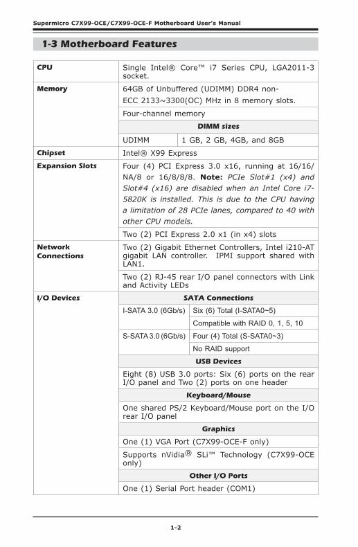
1-3 Motherboard Features
CPU Single Intel® Core™ i7 Series CPU, LGA2011-3 socket.
Memory 64GB of Unbuffered (UDIMM) DDR4 non-ECC 2133~3300(OC) MHz in 8 memory slots.
Four-channel memory
DIMM sizes
UDIMM 1 GB, 2 GB, 4GB, and 8GB
Chipset Intel® X99 Express
Expansion Slots Four (4) PCI Express 3.0 x16, running at 16/16/NA/8 or 16/8/8/8. Note: PCIe Slot#1 (x4) and Slot#4 (x16) are disabled when an Intel Core i7-5820K is installed. This is due to the CPU having a limitation of 28 PCIe lanes, compared to 40 with other CPU models.
Two (2) PCI Express 2.0 x1 (in x4) slots
Network Connections
Two (2) Gigabit Ethernet Controllers, Intel i210-AT gigabit LAN controller. IPMI support shared with LAN1.
Two (2) RJ-45 rear I/O panel connectors with Link and Activity LEDs
I/O Devices SATA Connections
I-SATA 3.0 (6Gb/s) Six (6) Total (I-SATA0~5)
Compatible with RAID 0, 1, 5, 10
S-SATA 3.0 (6Gb/s) Four (4) Total (S-SATA0~3)
No RAID support
USB Devices
Eight (8) USB 3.0 ports: Six (6) ports on the rear I/O panel and Two (2) ports on one header
Keyboard/Mouse
One shared PS/2 Keyboard/Mouse port on the I/O rear I/O panel
Graphics
One (1) VGA Port (C7X99-OCE-F only)
Supports nVidia® SLi™ Technology (C7X99-OCE only)
Other I/O Ports
One (1) Serial Port header (COM1)
Chapter 1: Introduction
1-3
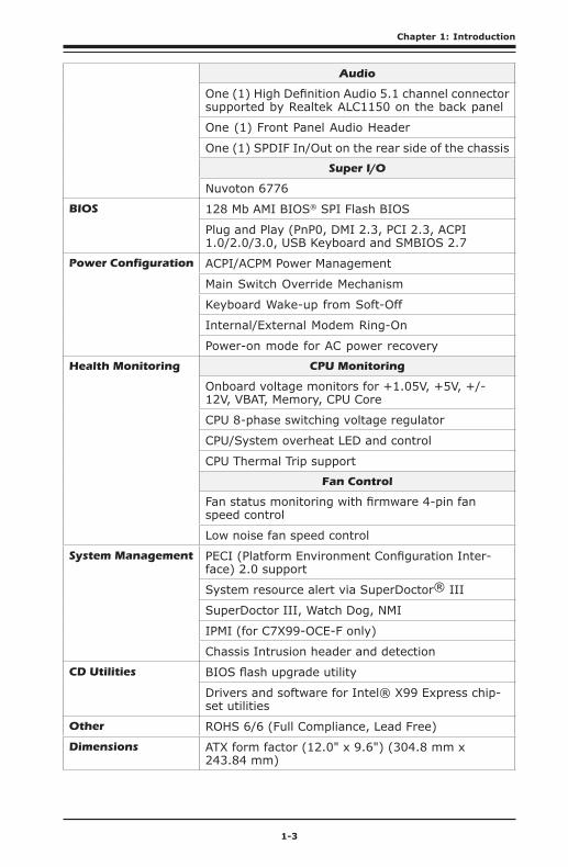
Audio
One (1) High Definition Audio 5.1 channel connector supported by Realtek ALC1150 on the back panel
One (1) Front Panel Audio Header
One (1) SPDIF In/Out on the rear side of the chassis
Super I/O
Nuvoton 6776
BIOS 128 Mb AMI BIOS® SPI Flash BIOS
Plug and Play (PnP0, DMI 2.3, PCI 2.3, ACPI 1.0/2.0/3.0, USB Keyboard and SMBIOS 2.7
Power Configuration ACPI/ACPM Power Management
Main Switch Override Mechanism
Keyboard Wake-up from Soft-Off
Internal/External Modem Ring-On
Power-on mode for AC power recovery
Health Monitoring CPU Monitoring
Onboard voltage monitors for +1.05V, +5V, +/-12V, VBAT, Memory, CPU Core
CPU 8-phase switching voltage regulator
CPU/System overheat LED and control
CPU Thermal Trip support
Fan Control
Fan status monitoring with firmware 4-pin fan speed control
Low noise fan speed control
System Management PECI (Platform Environment Configuration Inter-face) 2.0 support
System resource alert via SuperDoctor® III
SuperDoctor III, Watch Dog, NMI
IPMI (for C7X99-OCE-F only)
Chassis Intrusion header and detection
CD Utilities BIOS flash upgrade utility
Drivers and software for Intel® X99 Express chip-set utilities
Other ROHS 6/6 (Full Compliance, Lead Free)
Dimensions ATX form factor (12.0" x 9.6") (304.8 mm x 243.84 mm)
1-4
Supermicro C7X99-OCE/C7X99-OCE-F Motherboard User’s Manual
1-4 Special Features
Recovery from AC Power Loss
Basic I/O System (BIOS) provides a setting for you to determine how the system will respond when AC power is lost and then restored to the system. You can choose for the system to remain powered off, (in which case you must press the power switch to turn it back on), or for it to automatically return to a power-on state. See the Advanced BIOS Setup section to change this setting. The default setting is Last State.
1-5 PC Health Monitoring
This section describes the PC health monitoring features of the board. All have an onboard System Hardware Monitoring chip that supports PC health monitoring. An onboard voltage monitor will scan these onboard voltages continuously: +1.05V, +5V, +/-12V, VBAT, Memory, CPU Core. Once a voltage becomes unstable, a warning is given, or an error mes-sage is sent to the screen. The user can adjust the voltage thresholds to define the sensitivity of the voltage monitor.
Fan Status Monitor with Firmware Control
PC health monitoring in the BIOS can check the RPM status of the cool-ing fans. The onboard CPU and chassis fans are controlled by Thermal Management via SIO.
Environmental Temperature Control
The thermal control sensor monitors the CPU temperature in real time and will turn on the thermal control fan whenever the CPU temperature exceeds a user-defined threshold. The overheat circuitry runs indepen-dently from the CPU. Once the thermal sensor detects that the CPU temperature is too high, it will automatically turn on the thermal fans to prevent the CPU from overheating. The onboard chassis thermal circuitry can monitor the overall system temperature and alert the user when the chassis temperature is too high.
Note: To avoid possible system overheating, please be sure to provide adequate airflow to your system.
Chapter 1: Introduction
1-5
System Resource Alert
This feature is available when the system is used with SuperDoctor III in the Windows OS environment or used with SuperDoctor II in Linux. SuperDoctor is used to notify the user of certain system events. For example, you can also configure SuperDoctor to provide you with warnings when the system temperature, CPU temperatures, voltages and fan speeds go beyond predefined thresholds.
1-6 ACPI Features
ACPI stands for Advanced Configuration and Power Interface. The ACPI specification defines a flexible and abstract hardware interface that provides a standard way to integrate power management features throughout a PC system, including its hardware, operating system and application software. This enables the system to automatically turn on and off peripherals such as CD-ROMs, network cards, hard disk drives and printers.
In addition to enabling operating system-directed power management, ACPI also provides a generic system event mechanism for Plug and Play, and an operating system-independent interface for configuration control. ACPI leverages the Plug and Play BIOS data structures, while providing a processor architecture-independent implementation that is compatible with Windows 7, Windows 8, and Windows 2008 Operating Systems.
Slow Blinking LED for Suspend-State Indicator
When the CPU goes into a suspend state, the chassis power LED will start to blink to indicate that the CPU is in suspend mode. When the user presses any key, the CPU will "wake up", and the LED will automatically stop blinking and remain on.
1-6
Supermicro C7X99-OCE/C7X99-OCE-F Motherboard User’s Manual
1-7 Power Supply
As with all computer products, a stable power source is necessary for proper and reliable operation. It is even more important for processors that have high CPU clock rates.
This motherboard accommodates 24-pin ATX power supplies. Although most power supplies generally meet the specifications required by the CPU, some are inadequate. In addition, the 12V 8-pin power connector located at JPW2 is also required to ensure adequate power supply to the system. Also your power supply must supply 1.5A for the Ethernet ports.
Attention! To prevent damage to the power supply or mother-board, please use a power supply that contains a 24-pin and a 8-pin power connectors. Be sure to connect these connectors to the 24-pin (JPW1) and the 8-pin (JPW2) power connectors on the motherboard.
It is strongly recommended that you use a high quality power supply that meets ATX power supply Specification 2.02 or above. It must also be SSI compliant. (For more information, please refer to the web site at http://www.ssiforum.org/). Additionally, in areas where noisy power transmission is present, you may choose to install a line filter to shield the computer from noise. It is recommended that you also install a power surge protector to help avoid problems caused by power surges.
1-8 Super I/O
The Super I/O supports two high-speed, 16550 compatible serial commu-nication ports (UARTs). Each UART includes a 16-byte send/receive FIFO, a programmable baud rate generator, complete modem control capability and a processor interrupt system. Both UARTs provide legacy speed with baud rate of up to 115.2 Kbps as well as an advanced speed with baud rates of 250 K, 500 K, or 1 Mb/s, which support higher speed modems.
The Super I/O provides functions that comply with ACPI (Advanced Con-figuration and Power Interface), which includes support of legacy and ACPI power management through an SMI or SCI function pin. It also features auto power management to reduce power consumption.
Chapter 1: Introduction
1-7
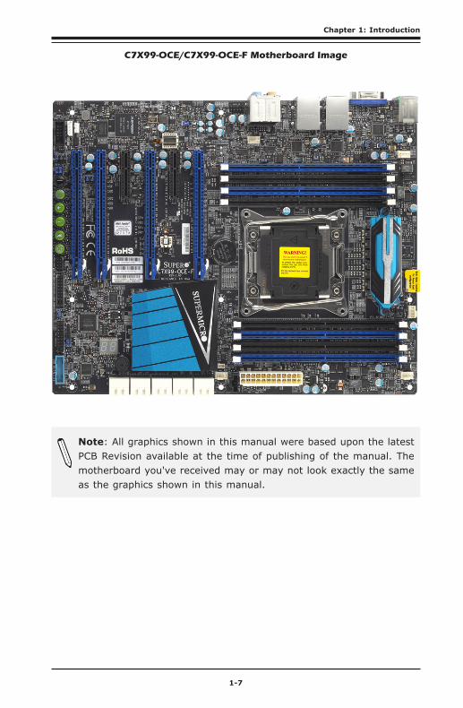
C7X99-OCE/C7X99-OCE-F Motherboard Image
Note: All graphics shown in this manual were based upon the latest PCB Revision available at the time of publishing of the manual. The motherboard you've received may or may not look exactly the same as the graphics shown in this manual.
1-8
Supermicro C7X99-OCE/C7X99-OCE-F Motherboard User’s Manual
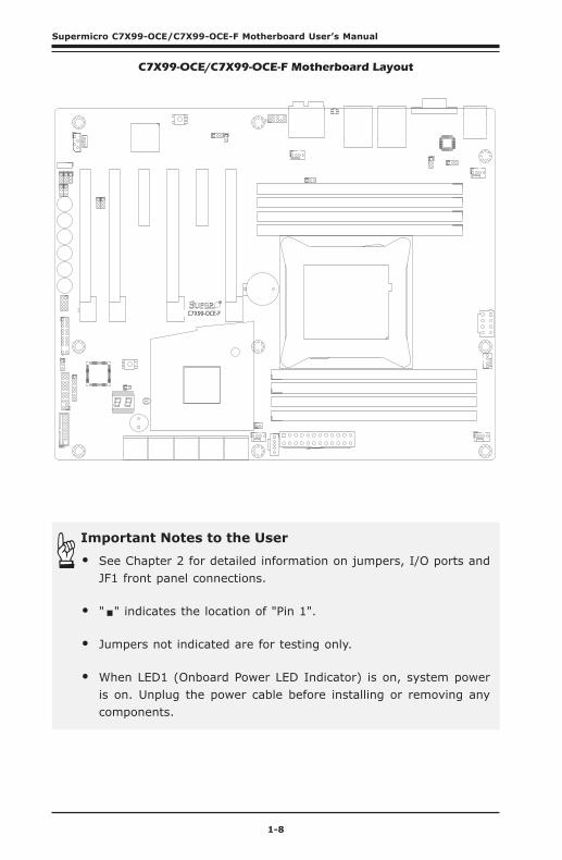
C7X99-OCE/C7X99-OCE-F Motherboard Layout
C7X99-OCE-F
S11
JUSB30_I2
MH
2
1
4
1
1
19
Important Notes to the User
• See Chapter 2 for detailed information on jumpers, I/O ports and JF1 front panel connections.
• " " indicates the location of "Pin 1".
• Jumpers not indicated are for testing only.
• When LED1 (Onboard Power LED Indicator) is on, system power is on. Unplug the power cable before installing or removing any components.
Chapter 1: Introduction
1-9
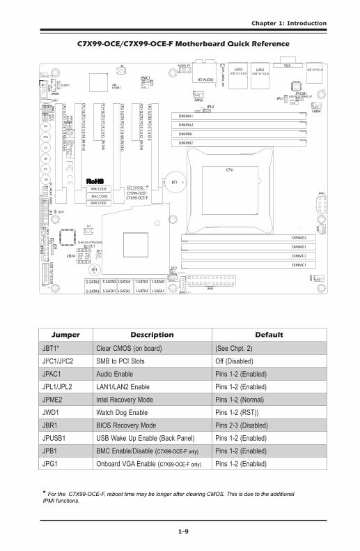
C7X99-OCE/C7X99-OCE-F Motherboard Quick Reference
MAC CODE
IPMI CODE
BAR CODEC7X99-OCE-F
SW_BIOSRC
S4
S7
S10
S5
S6
S9
OC_FRO
NT_PAN
EL
S8
S11
CLR_CMO
S_SW
JUSB30_I2
JAUD
IO1
LED4
I-SATA0I-SATA2I-SATA4S-SATA0S-SATA2
AUDIO_FP
JIPMB1
JSD1
MH11
MH
2
MH9
MH10
JPW2
C A
LEDM1
JBT1
BT1
+
FAN5
FAN4
FAN1
1
FAN2
4FAN3
JPL2
JPUSB1
J29J30
JPME2
JPAC1
JPL1
JI2C1JI2C2
JPB1
JPG1
JWD
11
JL2
JL1
JD1
1JF1
2
19
JPI2C1
JSTBY1
JTPM1
SP1
+
HD AUDIO
VGALAN1LAN2
USB 16/17(3.0)
USB 12/13(3.0) USB 10/11(3.0)USB 14/15(3.0)
CPU SLOT6 PCI-E 3.0 X16
PCH SLOT5 PCI-E 2.0 X1 (IN X4)
CPU SLOT4 PCI-E 3.0 X8 (IN X16)
PCH SLOT3 PCI-E 2.0 X1 (IN X4)
CPU SLOT2 PCI-E 3.0 X8 (IN X16)
CPU SLOT1 PCI-E 3.0 X8 (IN X16)
2-3:DISABLE
1-2:ENABLE
:WATCH
DO
G
SPEAKERPW
R LED
:TPM/PO
RT80
CPU
CHASSIS INTRUSION
JI2C2
2-3:DISABLE
1-2:ENABLE
JI2C1
PWR O
NO
H/FF
NIC1
NIC2
RSTX
CMO
S CLEAR
1-2:NORMAL2-3:BIOS RECOVERY
JBR1
PWR LED
HD
D LED
NM
IX
2-3:ME M
ANU
FACTURIN
G M
OD
E
JPME2
1-2:NO
RMAL
1-2 ENABLE2-3 DISABLE
1-2 ENABLE2-3 DISABLE
:PWR I2C1-2 EN
ABLE2-3 D
ISABLE
2-3 DISABLE
1-2 ENABLE
1-2 ENABLE2-3 DISABLE
JPAC1
VGA
USB14/15 WAKE UP
1-2 RST2-3 N
MI
:SATA DOM POWER
DIMMD2
DIMMD1
DIMMC2
DIMMC1
DIMMB2
DIMMB1
DIMMA2
DIMMA1
JBR1
JWD
1
JPW1
JPUSB1
JPB1JPG
1
C
A
LED1
I-SATA1I-SATA3I-SATA5S-SATA1S-SATA3
C7X99-OCE/
COM1
Jumper Description Default
JBT1* Clear CMOS (on board) (See Chpt. 2)JI2C1/JI2C2 SMB to PCI Slots Off (Disabled)JPAC1 Audio Enable Pins 1-2 (Enabled)JPL1/JPL2 LAN1/LAN2 Enable Pins 1-2 (Enabled)JPME2 Intel Recovery Mode Pins 1-2 (Normal)JWD1 Watch Dog Enable Pins 1-2 (RST))JBR1 BIOS Recovery Mode Pins 2-3 (Disabled)JPUSB1 USB Wake Up Enable (Back Panel) Pins 1-2 (Enabled)JPB1 BMC Enable/Disable (C7X99-OCE-F only) Pins 1-2 (Enabled)JPG1 Onboard VGA Enable (C7X99-OCE-F only) Pins 1-2 (Enabled)
* For the C7X99-OCE-F, reboot time may be longer after clearing CMOS. This is due to the additional IPMI functions.
1-10
Supermicro C7X99-OCE/C7X99-OCE-F Motherboard User’s Manual
**Download the AMI status codes at http://www.ami.com/support/doc/ami_aptio_4.x_status_codes_pub.pdf
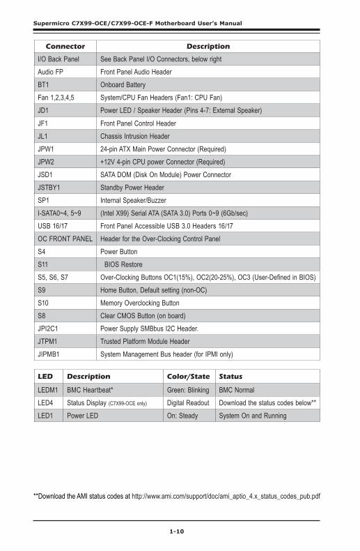
LED Description Color/State Status
LEDM1 BMC Heartbeat* Green: Blinking BMC NormalLED4 Status Display (C7X99-OCE only) Digital Readout Download the status codes below**LED1 Power LED On: Steady System On and Running
Connector Description
I/O Back Panel See Back Panel I/O Connectors, below rightAudio FP Front Panel Audio HeaderBT1 Onboard BatteryFan 1,2,3,4,5 System/CPU Fan Headers (Fan1: CPU Fan)JD1 Power LED / Speaker Header (Pins 4-7: External Speaker)
JF1 Front Panel Control HeaderJL1 Chassis Intrusion HeaderJPW1 24-pin ATX Main Power Connector (Required)JPW2 +12V 4-pin CPU power Connector (Required)JSD1 SATA DOM (Disk On Module) Power ConnectorJSTBY1 Standby Power HeaderSP1 Internal Speaker/BuzzerI-SATA0~4, 5~9 (Intel X99) Serial ATA (SATA 3.0) Ports 0~9 (6Gb/sec)USB 16/17 Front Panel Accessible USB 3.0 Headers 16/17OC FRONT PANEL Header for the Over-Clocking Control PanelS4 Power ButtonS11 BIOS RestoreS5, S6, S7 Over-Clocking Buttons OC1(15%), OC2(20-25%), OC3 (User-Defined in BIOS)S9 Home Button, Default setting (non-OC)S10 Memory Overclocking ButtonS8 Clear CMOS Button (on board)JPI2C1 Power Supply SMBbus I2C Header.JTPM1 Trusted Platform Module HeaderJIPMB1 System Management Bus header (for IPMI only)
Chapter 1: Introduction
1-11
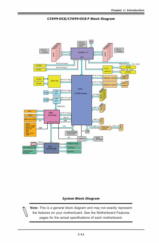
System Block Diagram
Note: This is a general block diagram and may not exactly represent the features on your motherboard. See the Motherboard Features
pages for the actual specifications of each motherboard.
8 PHASE145W
VR12.5
PCI-E X16 Gen3
PCI-E X8 Gen3
DMI
LGA2011-3
I210LAN PCI-E X1 Gen2
SPI
Debug Card
CTRLFAN SPEED
PCI-E X1 Gen2
USB 2.0
XDP
XDP
PCH
C7X99 Series 6.0 Gb/S
USB 2.0
LPC
US
B
#1#0
SA
TA
#4#3#2
SMB
PCI-E X8 Gen3JPCIE2
JPCIE1
PCI-E X1 Gen2LAN
TPM HEADER
I210
USB 3.0
RJ45
RJ45
ASM1182ePCI-E X1 Gen2
BIOSSPI ROM
SPI
CRT
JPCIE3
JPCIE5
US
B
ASMedia 1042AEUSB3.0
AST2400BMC
ASMedia 1042AE
RMII/NCSI
USB2.0
USB3.0
BMC Boot Flash
USB2.0
DDR3
SIONCT6776F
SPI
SMB
IPMBPower supplyMemory VRCPU VRXDPI210PCIE SLOTTPM
PCI-E
SWITCH
80 port
Temp SensorRT1RT2
Voltage monitor
COM Port
PS2 Port
SWITCH
PCI-E X1 Gen2
PCI-E X1 Gen2
FERICOMrepeater
USB 3.0
US
BUSB 3.0
2 PHASEVR12.5
2 PHASEVR12.5
#0-4#0-3
#0-2#0-1
DD
R4
DD
R4
#0-8#0-7
#0-6#0-5
JPCIE6PCI-E X16 or X8 Gen3
JPCIE4
#5#7#8#9
C7X99-OCE/C7X99-OCE-F Block Diagram

1-12
Supermicro C7X99-OCE/C7X99-OCE-F Motherboard User’s Manual
Notes
Chapter 2: Installation
2-1
Chapter 2
Installation
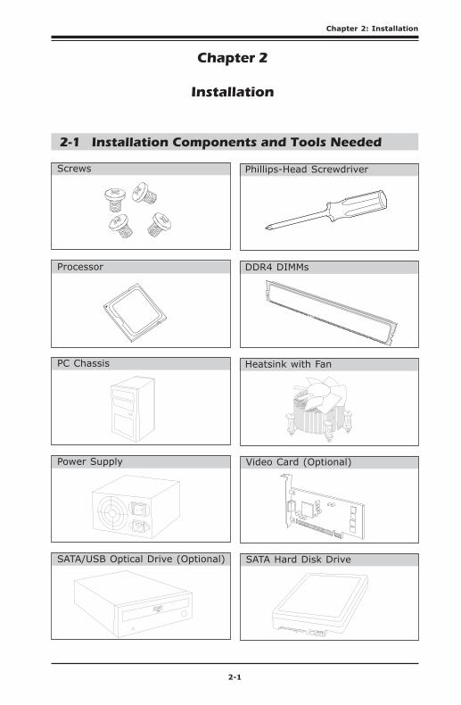
2-1 Installation Components and Tools Needed
Screws Phillips-Head Screwdriver
Processor DDR4 DIMMs
PC Chassis Heatsink with Fan
Power Supply Video Card (Optional)
SATA/USB Optical Drive (Optional) SATA Hard Disk Drive
2-2
Supermicro C7X99-OCE/C7X99-OCE-F Motherboard User’s Manual
2-2 Static-Sensitive Devices
Electrostatic-Discharge (ESD) can damage electronic com ponents. To avoid damaging your system board, it is important to handle it very carefully. The following measures are generally sufficient to protect your equipment from ESD.
Precautions
• Use a grounded wrist strap designed to prevent static discharge.
• Touch a grounded metal object before removing the board from the antistatic bag.
• Handle the board by its edges only; do not touch its components, peripheral chips, memory modules or gold contacts.
• When handling chips or modules, avoid touching their pins.
• Put the motherboard and peripherals back into their antistatic bags when not in use.
• For grounding purposes, make sure your computer chassis provides excellent conductivity between the power supply, the case, the mount-ing fasteners and the motherboard.
• Use only the correct type of onboard CMOS battery. Do not install the onboard battery upside down to avoid possible explosion.
Unpacking
The motherboard is shipped in antistatic packaging to avoid static dam-age. When unpacking the board, make sure that the person handling it is static protected.
Chapter 2: Installation
2-3
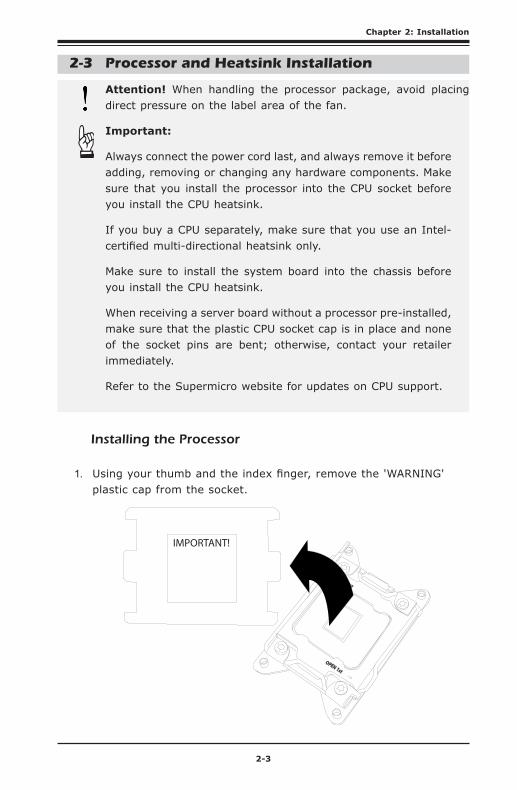
2-3 Processor and Heatsink Installation
Attention! When handling the processor package, avoid placing direct pressure on the label area of the fan.
Important:
Always connect the power cord last, and always remove it before adding, removing or changing any hardware components. Make sure that you install the processor into the CPU socket before you install the CPU heatsink.
If you buy a CPU separately, make sure that you use an Intel-certified multi-directional heatsink only.
Make sure to install the system board into the chassis before you install the CPU heatsink.
When receiving a server board without a processor pre-installed, make sure that the plastic CPU socket cap is in place and none of the socket pins are bent; otherwise, contact your retailer immediately.
Refer to the Supermicro website for updates on CPU support.
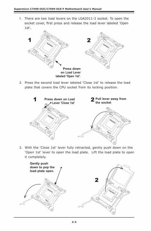
OPEN 1st
IMPORTANT!
1. Using your thumb and the index finger, remove the 'WARNING' plastic cap from the socket.
Installing the Processor
2-4
Supermicro C7X99-OCE/C7X99-OCE-F Motherboard User’s Manual
OPEN 1st
WARNING!
OPEN 1st
WARNING!
2. Press the second load lever labeled 'Close 1st' to release the load plate that covers the CPU socket from its locking position.
3. With the 'Close 1st' lever fully retracted, gently push down on the 'Open 1st' lever to open the load plate. Lift the load plate to open it completely.
OPEN 1st
WARNING!
OPEN 1st
WARNING!
2 Press down on Load Lever 'Close 1st'
WARNING!
Pull lever away from the socket
2
Gently push down to pop the load plate open.
1
Press down on Load Lever
labeled 'Open 1st'.
1 2
OPEN 1st
WARNING!
1. There are two load levers on the LGA2011-3 socket. To open the socket cover, first press and release the load lever labeled 'Open 1st'.
Chapter 2: Installation
2-5
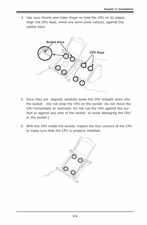
Socket Keys
CPU Keys
4. Use your thumb and index finger to hold the CPU on its edges. Align the CPU keys, which are semi-circle cutouts, against the socket keys.
5. Once they are aligned, carefully lower the CPU straight down into the socket. (Do not drop the CPU on the socket. Do not move the CPU horizontally or vertically. Do not rub the CPU against the sur-face or against any pins of the socket to avoid damaging the CPU or the socket.)
6. With the CPU inside the socket, inspect the four corners of the CPU to make sure that the CPU is properly installed.
2-6
Supermicro C7X99-OCE/C7X99-OCE-F Motherboard User’s Manual
OPEN 1st
OPEN 1st
OPEN 1st
Lever Lock
Lever Lock
Push down and lock 'Open 1st'
lever
Push down and lock 'Close 1st' lever.
Gently close the load plate.1 2
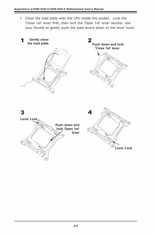
3 4
7. Close the load plate with the CPU inside the socket. Lock the 'Close 1st' lever first, then lock the 'Open 1st' lever second. Use your thumb to gently push the load levers down to the lever locks.
Chapter 2: Installation
2-7
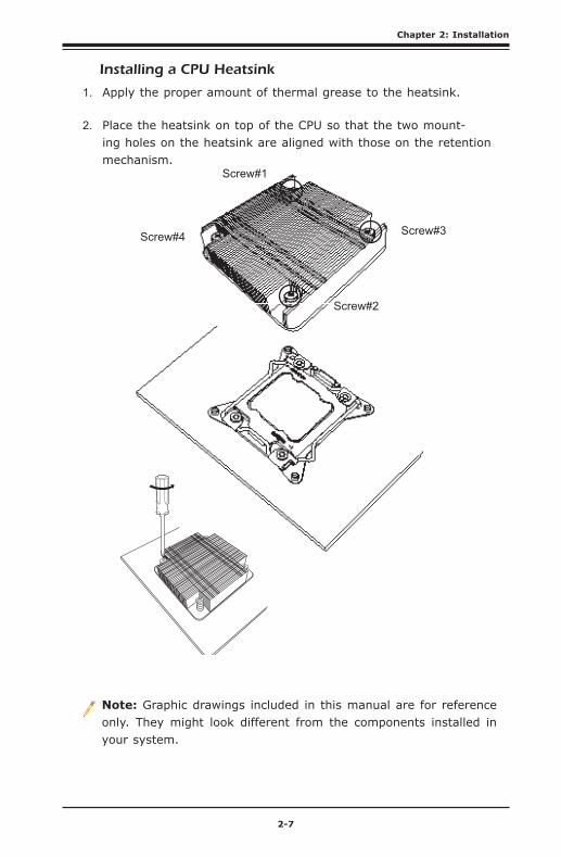
Installing a CPU Heatsink
1. Apply the proper amount of thermal grease to the heatsink.
2. Place the heatsink on top of the CPU so that the two mount-ing holes on the heatsink are aligned with those on the retention mechanism.
Note: Graphic drawings included in this manual are for reference only. They might look different from the components installed in your system.
Screw#1
Screw#3Screw#4
Screw#2

2-8
Supermicro C7X99-OCE/C7X99-OCE-F Motherboard User’s Manual
Removing a Heatsink
Warning: We do not recommend that the CPU or the heatsink be removed. However, if you do need to remove the heatsink, please follow the instruc-tions below to uninstall the heatsink to avoid damaging the CPU or other components.
1. Unplug the power cord from the power supply.
2. Loosen the screws.
3. Gently wriggle the heatsink to loosen it. (Do not use excessive force when wriggling the heatsink.)
4. Once the heatsink is loosened, remove it from the motherboard.
Chapter 2: Installation
2-9
MAC CODE
IPMI CODE
BAR CODEC7X99-OCE-F
SW_BIOSRC
S4
S7
S10
S5
S6
S9
OC_FRO
NT_PAN
EL
S8
S11
CLR_CMO
S_SW
JUSB30_I2
JAUD
IO1
LED4
I-SATA0I-SATA2I-SATA4S-SATA0S-SATA2
AUDIO_FP
JIPMB1
JSD1
MH11
MH
2
MH9
MH10
JPW2
C A
LEDM1
JBT1
BT1
+
FAN5
FAN4
FAN1
1
FAN2
4FAN3
JPL2
JPUSB1
J29J30
JPME2
JPAC1
JPL1JI2C1JI2C2
JPB1
JPG1
JWD
11
JL2
JL1
JD1
1JF1
2
19
JPI2C1
JSTBY1
JTPM1
SP1
+
HD AUDIO
VGALAN1LAN2
USB 16/17(3.0)
USB 12/13(3.0) USB 10/11(3.0)USB 14/15(3.0)
CPU SLOT6 PCI-E 3.0 X16
PCH SLOT5 PCI-E 2.0 X1 (IN X4)
CPU SLOT4 PCI-E 3.0 X8 (IN X16)
PCH SLOT3 PCI-E 2.0 X1 (IN X4)
CPU SLOT2 PCI-E 3.0 X8 (IN X16)
CPU SLOT1 PCI-E 3.0 X8 (IN X16)
2-3:DISABLE
1-2:ENABLE
:WATCH
DO
G
SPEAKERPW
R LED
:TPM/PO
RT80
CPU
CHASSIS INTRUSION
JI2C2
2-3:DISABLE
1-2:ENABLE
JI2C1
PWR O
NO
H/FF
NIC1
NIC2
RSTX
CMO
S CLEAR
1-2:NORMAL2-3:BIOS RECOVERY
JBR1
PWR LED
HD
D LED
NM
IX
2-3:ME M
ANU
FACTURIN
G M
OD
E
JPME2
1-2:NO
RMAL
1-2 ENABLE2-3 DISABLE
1-2 ENABLE2-3 DISABLE
:PWR I2C
1-2 ENABLE
2-3 DISABLE
2-3 DISABLE
1-2 ENABLE
1-2 ENABLE2-3 DISABLE
JPAC1
VGA
USB14/15 WAKE UP
1-2 RST2-3 N
MI
:SATA DOM POWER
DIMMD2
DIMMD1
DIMMC2
DIMMC1
DIMMB2
DIMMB1
DIMMA2
DIMMA1
JBR1JW
D1
JPW1
JPUSB1
JPB1JPG
1
C
A
LED1
I-SATA1I-SATA3I-SATA5S-SATA1S-SATA3
C7X99-OCE/
COM1
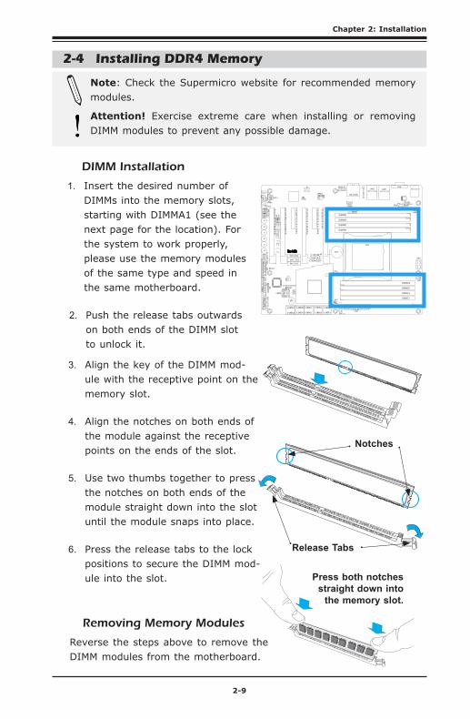
2-4 Installing DDR4 Memory
Note: Check the Supermicro website for recommended memory modules.
Attention! Exercise extreme care when installing or removing DIMM modules to prevent any possible damage.
DIMM Installation
1. Insert the desired number of DIMMs into the memory slots, starting with DIMMA1 (see the next page for the location). For the system to work properly, please use the memory modules of the same type and speed in the same motherboard.
Release Tabs
Notches
2. Push the release tabs outwards on both ends of the DIMM slot to unlock it.
Press both notches straight down into
the memory slot.
3. Align the key of the DIMM mod-ule with the receptive point on the memory slot.
4. Align the notches on both ends of the module against the receptive points on the ends of the slot.
5. Use two thumbs together to press the notches on both ends of the module straight down into the slot until the module snaps into place.
6. Press the release tabs to the lock positions to secure the DIMM mod-ule into the slot.
Removing Memory Modules
Reverse the steps above to remove the DIMM modules from the motherboard.
2-10
Supermicro C7X99-OCE/C7X99-OCE-F Motherboard User’s Manual
Memory SupportTowards the CPU
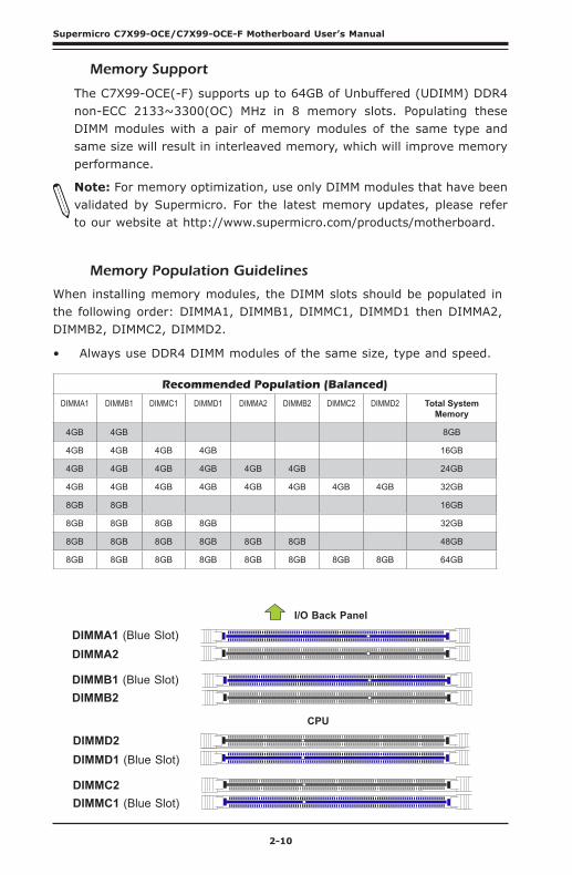
Memory Population Guidelines
When installing memory modules, the DIMM slots should be populated in the following order: DIMMA1, DIMMB1, DIMMC1, DIMMD1 then DIMMA2, DIMMB2, DIMMC2, DIMMD2.
• Always use DDR4 DIMM modules of the same size, type and speed.
Recommended Population (Balanced)
DIMMA1 DIMMB1 DIMMC1 DIMMD1 DIMMA2 DIMMB2 DIMMC2 DIMMD2 Total System Memory
4GB 4GB 8GB
4GB 4GB 4GB 4GB 16GB
4GB 4GB 4GB 4GB 4GB 4GB 24GB
4GB 4GB 4GB 4GB 4GB 4GB 4GB 4GB 32GB
8GB 8GB 16GB
8GB 8GB 8GB 8GB 32GB
8GB 8GB 8GB 8GB 8GB 8GB 48GB
8GB 8GB 8GB 8GB 8GB 8GB 8GB 8GB 64GB
The C7X99-OCE(-F) supports up to 64GB of Unbuffered (UDIMM) DDR4 non-ECC 2133~3300(OC) MHz in 8 memory slots. Populating these DIMM modules with a pair of memory modules of the same type and same size will result in interleaved memory, which will improve memory performance.
Note: For memory optimization, use only DIMM modules that have been validated by Supermicro. For the latest memory updates, please refer to our website at http://www.supermicro.com/products/motherboard.
CPU
DIMMB2
DIMMA2DIMMA1 (Blue Slot)
DIMMB1 (Blue Slot)
DIMMC1 (Blue Slot)
DIMMD1 (Blue Slot)DIMMD2
DIMMC2
I/O Back Panel
Chapter 2: Installation
2-11
Notes
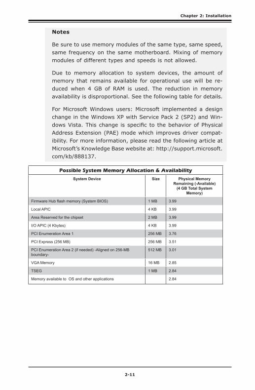
Be sure to use memory modules of the same type, same speed, same frequency on the same motherboard. Mixing of memory modules of different types and speeds is not allowed.
Due to memory allocation to system devices, the amount of memory that remains available for operational use will be re-duced when 4 GB of RAM is used. The reduction in memory availability is disproportional. See the following table for details.
For Microsoft Windows users: Microsoft implemented a design change in the Windows XP with Service Pack 2 (SP2) and Win-dows Vista. This change is specific to the behavior of Physical Address Extension (PAE) mode which improves driver compat-ibility. For more information, please read the following article at Microsoft’s Knowledge Base website at: http://support.microsoft.com/kb/888137.
Possible System Memory Allocation & Availability
System Device Size Physical Memory Remaining (-Available)
(4 GB Total System Memory)
Firmware Hub flash memory (System BIOS) 1 MB 3.99
Local APIC 4 KB 3.99
Area Reserved for the chipset 2 MB 3.99
I/O APIC (4 Kbytes) 4 KB 3.99
PCI Enumeration Area 1 256 MB 3.76
PCI Express (256 MB) 256 MB 3.51
PCI Enumeration Area 2 (if needed) -Aligned on 256-MB boundary-
512 MB 3.01
VGA Memory 16 MB 2.85
TSEG 1 MB 2.84
Memory available to OS and other applications 2.84
2-12
Supermicro C7X99-OCE/C7X99-OCE-F Motherboard User’s Manual
MAC CODE
IPMI CODE
BAR CODEC7X99-OCE-F
SW_BIOSRC
S4
S7
S10
S5
S6
S9
OC_FRO
NT_PAN
EL
S8
S11
CLR_CMO
S_SW
JUSB30_I2
JAUD
IO1
LED4
I-SATA0I-SATA2I-SATA4S-SATA0S-SATA2
AUDIO_FP
JIPMB1
JSD1
MH11
MH
2
MH9
MH10
JPW2C A
LEDM1
JBT1
BT1
+
FAN5
FAN4
FAN1
1
FAN2
4FAN3
JPL2
JPUSB1
J29J30
JPME2
JPAC1
JPL1
JI2C1JI2C2
JPB1
JPG1
JWD
11
JL2
JL1
JD1
1JF1
2
19
JPI2C1
JSTBY1
JTPM1
SP1
+
HD AUDIO
VGALAN1LAN2
USB 16/17(3.0)
USB 12/13(3.0) USB 10/11(3.0)USB 14/15(3.0)
CPU SLOT6 PCI-E 3.0 X16
PCH SLOT5 PCI-E 2.0 X1 (IN X4)
CPU SLOT4 PCI-E 3.0 X8 (IN X16)
PCH SLOT3 PCI-E 2.0 X1 (IN X4)
CPU SLOT2 PCI-E 3.0 X8 (IN X16)
CPU SLOT1 PCI-E 3.0 X8 (IN X16)
2-3:DISABLE
1-2:ENABLE
:WATCH
DO
G
SPEAKERPW
R LED
:TPM/PO
RT80
CPU
CHASSIS INTRUSION
JI2C2
2-3:DISABLE
1-2:ENABLE
JI2C1
PWR O
NO
H/FF
NIC1
NIC2
RSTX
CMO
S CLEAR
1-2:NORMAL2-3:BIOS RECOVERY
JBR1
PWR LED
HD
D LED
NM
IX
2-3:ME M
ANU
FACTURIN
G M
OD
E
JPME2
1-2:NO
RMAL
1-2 ENABLE2-3 DISABLE
1-2 ENABLE2-3 DISABLE
:PWR I2C
1-2 ENABLE
2-3 DISABLE
2-3 DISABLE
1-2 ENABLE
1-2 ENABLE2-3 DISABLE
JPAC1
VGA
USB14/15 WAKE UP
1-2 RST2-3 N
MI
:SATA DOM POWER
DIMMD2
DIMMD1
DIMMC2
DIMMC1
DIMMB2
DIMMB1
DIMMA2
DIMMA1
JBR1
JWD
1
JPW1
JPUSB1
JPB1JPG
1
C
A
LED1
I-SATA1I-SATA3I-SATA5S-SATA1S-SATA3
C7X99-OCE/
COM1
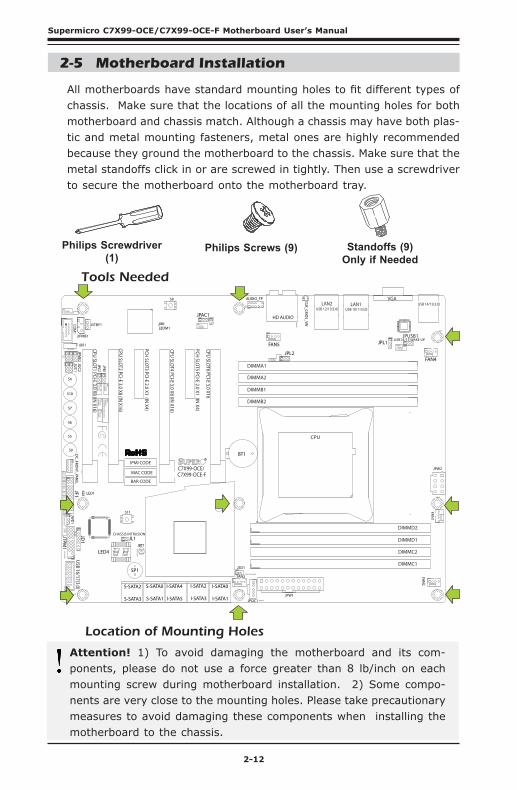
Location of Mounting Holes
Attention! 1) To avoid damaging the motherboard and its com-ponents, please do not use a force greater than 8 lb/inch on each mounting screw during motherboard installation. 2) Some compo-nents are very close to the mounting holes. Please take precautionary measures to avoid damaging these components when installing the motherboard to the chassis.
2-5 Motherboard Installation
All motherboards have standard mounting holes to fit different types of chassis. Make sure that the locations of all the mounting holes for both motherboard and chassis match. Although a chassis may have both plas-tic and metal mounting fasteners, metal ones are highly recommended because they ground the motherboard to the chassis. Make sure that the metal standoffs click in or are screwed in tightly. Then use a screwdriver to secure the motherboard onto the motherboard tray.
Philips Screwdriver (1)
Standoffs (9)Only if Needed
Philips Screws (9)
Tools Needed
Chapter 2: Installation
2-13
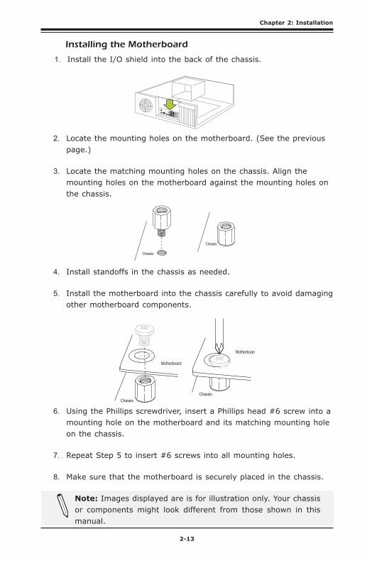
Installing the Motherboard
1. Install the I/O shield into the back of the chassis.
2. Locate the mounting holes on the motherboard. (See the previous page.)
3. Locate the matching mounting holes on the chassis. Align the mounting holes on the motherboard against the mounting holes on the chassis.
4. Install standoffs in the chassis as needed.
5. Install the motherboard into the chassis carefully to avoid damaging other motherboard components.
6. Using the Phillips screwdriver, insert a Phillips head #6 screw into a mounting hole on the motherboard and its matching mounting hole on the chassis.
7. Repeat Step 5 to insert #6 screws into all mounting holes.
8. Make sure that the motherboard is securely placed in the chassis.
Note: Images displayed are is for illustration only. Your chassis or components might look different from those shown in this manual.
2-14
Supermicro C7X99-OCE/C7X99-OCE-F Motherboard User’s Manual
MAC CODE
IPMI CODE
BAR CODEC7X99-OCE-F
SW_BIOSRC
S4
S7
S10
S5
S6
S9
OC_FRO
NT_PAN
EL
S8
S11
CLR_CMO
S_SW
JUSB30_I2
JAUD
IO1
LED4
I-SATA0I-SATA2I-SATA4S-SATA0S-SATA2
AUDIO_FP
JIPMB1
JSD1
MH11
MH
2
MH9
MH10
JPW2
C A
LEDM1
JBT1
BT1
+
FAN5
FAN4
FAN1
1
FAN2
4FAN3
JPL2
JPUSB1
J29J30
JPME2
JPAC1
JPL1
JI2C1JI2C2
JPB1
JPG1
JWD
11
JL2
JL1
JD1
1JF1
2
19
JPI2C1
JSTBY1
JTPM1
SP1
+
HD AUDIO
VGALAN1LAN2
USB 16/17(3.0)
USB 12/13(3.0) USB 10/11(3.0)USB 14/15(3.0)
CPU SLOT6 PCI-E 3.0 X16
PCH SLOT5 PCI-E 2.0 X1 (IN X4)
CPU SLOT4 PCI-E 3.0 X8 (IN X16)
PCH SLOT3 PCI-E 2.0 X1 (IN X4)
CPU SLOT2 PCI-E 3.0 X8 (IN X16)
CPU SLOT1 PCI-E 3.0 X8 (IN X16)
2-3:DISABLE
1-2:ENABLE
:WATCH
DO
G
SPEAKERPW
R LED
:TPM/PO
RT80
CPU
CHASSIS INTRUSION
JI2C2
2-3:DISABLE
1-2:ENABLE
JI2C1
PWR O
NO
H/FF
NIC1
NIC2
RSTX
CMO
S CLEAR
1-2:NORMAL2-3:BIOS RECOVERY
JBR1
PWR LED
HD
D LED
NM
IX
2-3:ME M
ANU
FACTURIN
G M
OD
E
JPME2
1-2:NO
RMAL
1-2 ENABLE2-3 DISABLE
1-2 ENABLE2-3 DISABLE
:PWR I2C
1-2 ENABLE
2-3 DISABLE
2-3 DISABLE
1-2 ENABLE
1-2 ENABLE2-3 DISABLE
JPAC1
VGA
USB14/15 WAKE UP
1-2 RST2-3 N
MI
:SATA DOM POWER
DIMMD2
DIMMD1
DIMMC2
DIMMC1
DIMMB2
DIMMB1
DIMMA2
DIMMA1
JBR1
JWD
1
JPW1
JPUSB1
JPB1JPG
1
C
A
LED1
I-SATA1I-SATA3I-SATA5S-SATA1S-SATA3
C7X99-OCE/
COM1
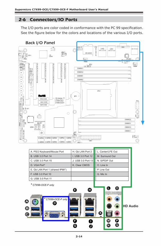
2-6 Connectors/IO Ports
The I/O ports are color coded in conformance with the PC 99 specification. See the figure below for the colors and locations of the various I/O ports.
Back I/O Panel
A. PS/2 Keyboard/Mouse Port H. Gb LAN Port 1 N. Center/LFE Out
B. USB 2.0 Port 0 I. USB 3.0 Port 2 O. Surround Out
C. USB 2.0 Port 1 J. USB 3.0 Port 3 P. S/PDIF Out
D. VGA Port K. Gb LAN Port 2 Q. Line In
E. DVI Port L. USB 3.0 Port 12 R. Line Out
F. VESA DisplayPort M. USB 3.0 Port 13 S. Mic In
G. HDMI Port
A. PS/2 Keyboard/Mouse Port H. Gb LAN Port 2 L. Center/LFE Out
B. USB 3.0 Port 14 I. USB 3.0 Port 12 M. Surround Out
C. USB 3.0 Port 15 J. USB 3.0 Port 13 N. S/PDIF Out
D. VGA Port* K. Clear CMOS O. Line In
E. Gb LAN Port 1 (shared IPMI*) P. Line Out
F. USB 3.0 Port 10 Q. Mic In
G. USB 3.0 Port 11
A
B
C
D
E
FG
H
IJ
K
L
MN
O
PQ
HD Audio
* C7X99-OCE-F only
* C7X99-OCE-F only
Chapter 2: Installation
2-15
MAC CODE
IPMI CODE
BAR CODEC7X99-OCE-F
SW_BIOSRC
S4
S7
S10
S5
S6
S9
OC_FRO
NT_PAN
EL
S8
S11
CLR_CMO
S_SW
JUSB30_I2
JAUD
IO1
LED4
I-SATA0I-SATA2I-SATA4S-SATA0S-SATA2
AUDIO_FP
JIPMB1
JSD1
MH11
MH
2
MH9
MH10
JPW2
C A
LEDM1
JBT1
BT1
+
FAN5
FAN4
FAN1
1
FAN2
4FAN3
JPL2
JPUSB1
J29J30
JPME2
JPAC1
JPL1
JI2C1JI2C2
JPB1
JPG1
JWD
11
JL2
JL1
JD1
1JF1
2
19
JPI2C1
JSTBY1
JTPM1
SP1
+
HD AUDIO
VGALAN1LAN2
USB 16/17(3.0)
USB 12/13(3.0) USB 10/11(3.0)USB 14/15(3.0)
CPU SLOT6 PCI-E 3.0 X16
PCH SLOT5 PCI-E 2.0 X1 (IN X4)
CPU SLOT4 PCI-E 3.0 X8 (IN X16)
PCH SLOT3 PCI-E 2.0 X1 (IN X4)
CPU SLOT2 PCI-E 3.0 X8 (IN X16)
CPU SLOT1 PCI-E 3.0 X8 (IN X16)
2-3:DISABLE
1-2:ENABLE
:WATCH
DO
G
SPEAKERPW
R LED
:TPM/PO
RT80
CPU
CHASSIS INTRUSION
JI2C2
2-3:DISABLE
1-2:ENABLE
JI2C1
PWR O
NO
H/FF
NIC1
NIC2
RSTX
CMO
S CLEAR
1-2:NORMAL2-3:BIOS RECOVERY
JBR1
PWR LED
HD
D LED
NM
IX
2-3:ME M
ANU
FACTURIN
G M
OD
E
JPME2
1-2:NO
RMAL
1-2 ENABLE2-3 DISABLE
1-2 ENABLE2-3 DISABLE
:PWR I2C
1-2 ENABLE
2-3 DISABLE
2-3 DISABLE
1-2 ENABLE
1-2 ENABLE2-3 DISABLE
JPAC1
VGA
USB14/15 WAKE UP
1-2 RST2-3 N
MI
:SATA DOM POWER
DIMMD2
DIMMD1
DIMMC2
DIMMC1
DIMMB2
DIMMB1
DIMMA2
DIMMA1
JBR1
JWD
1
JPW1
JPUSB1
JPB1JPG
1
C
A
LED1
I-SATA1I-SATA3I-SATA5S-SATA1S-SATA3
C7X99-OCE/
COM1
A. Backpanel USB 3.0 #14
B. Backpanel USB 3.0 #15
C. Backpanel USB 3.0 #10
D. Backpanel USB 3.0 #11
E. Backpanel USB 3.0 #12
F. Backpanel USB 3.0 #13
G. USB 3.0 Header #16/17
Universal Serial Bus (USB)
Six USB 3.0 ports (10/11, 12/13, 14/15) are located on the I/O back panel. In addition, one USB 3.0 header (USB 16/17) is also located on the motherboard to provide front chassis access using USB cables (not included). These ports are backward compatible with the USB 2.0 stan-dard. See the tables below for pin definitions.
Back Panel USB (2.0) #0/1, USB (3.0) #2/3, 12/13 Pin Definitions
Pin# Definition Pin# Definition
1 +5V 5 +5V
2 USB_PN1 6 USB_PN0
3 USB_PP1 7 USB_PP0
4 Ground 8 Ground
A
Front Panel USB (3.0) Header #14/15 Pin Definitions
Pin# Pin# Signal Name Description
1 10 VBUS Power
2 11 D- USB 2.0 Differential Pair
3 12 D+
4 13 Ground Ground of PWR Return
5 14 StdA_SSRX- SuperSpeed Receiver
6 15 StdA_SSRX+ Differential Pair
7 16 GND_DRAIN Ground for Signal Return
8 17 StdA_SSTX- SuperSpeed Transmitter
9 18 StdA_SSTX+ Differential Pair
C EB FD
G

2-16
Supermicro C7X99-OCE/C7X99-OCE-F Motherboard User’s Manual
Ethernet Ports
Two Gigabit Ethernet ports (LAN1/LAN2) are located next to the HD Audio Con-nector on the I/O Backpanel to provide network connections. These ports accept RJ45 type cables.
Note: Please refer to the LED Indica-tor Section for LAN LED information.
LAN PortsPin Definition
Pin# Definition Pin# Definition
1 P2V5SB 10 SGND
2 TD0+ 11 Act LED
3 TD0- 12 P3V3SB
4 TD1+ 13 Link 100 LED (Green, +3V3SB)
5 TD1- 14 Link 1000 LED (Yellow, +3V3SB)
6 TD2+ 15 Ground
7 TD2- 16 Ground
8 TD3+ 17 Ground
9 TD3- 88 Ground
(NC: No Connection)
A. LAN1
B. LAN2
C. Center/LFE Out
D. Surround Out
E. S/PDIF Out
F. Line In
G. Line Out
H. Mic In
Back Panel High Definition Audio (HD Audio)
This motherboard features a 5.1+2 Channel High Definition Audio (HDA) co-dec that provides 10 DAC channels. The HD Audio connections simultaneously supports multiple-streaming 5.1 sound playback with 2 channels of independent stereo output through the front panel stereo out for front, rear, center and subwoofer speakers. Use the Advanced software included in the CD-ROM with your motherboard to enable this func-tion.
A
E
B F
G
C
D
H
Chapter 2: Installation
2-17
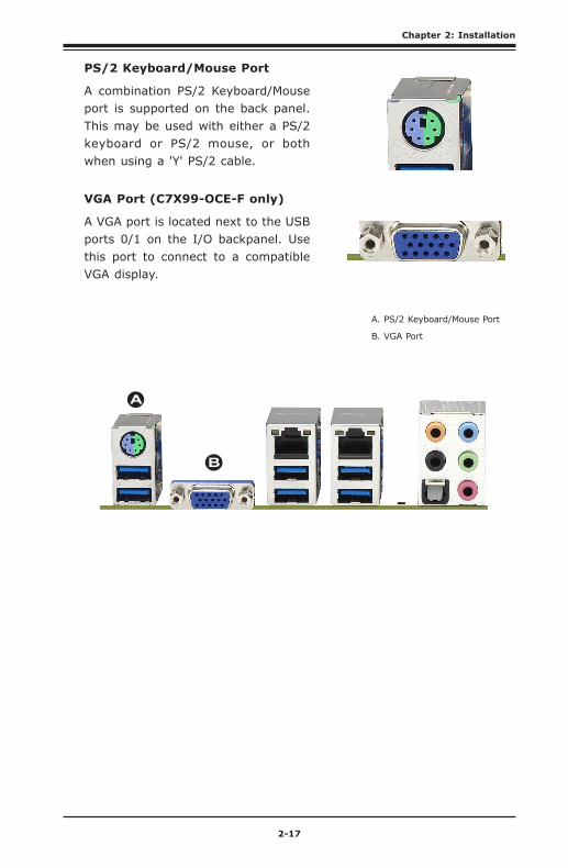
B
A
A. PS/2 Keyboard/Mouse Port
B. VGA Port
VGA Port (C7X99-OCE-F only)
A VGA port is located next to the USB ports 0/1 on the I/O backpanel. Use this port to connect to a compatible VGA display.
PS/2 Keyboard/Mouse Port
A combination PS/2 Keyboard/Mouse port is supported on the back panel. This may be used with either a PS/2 keyboard or PS/2 mouse, or both when using a 'Y' PS/2 cable.
2-18
Supermicro C7X99-OCE/C7X99-OCE-F Motherboard User’s Manual
C7X99-OCE-F
S11
JUSB30_I2
MH
2
1
4
1
1
19
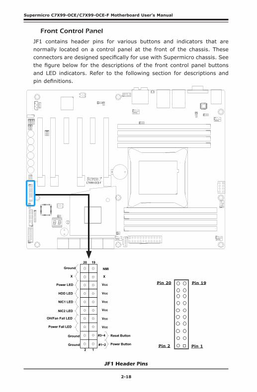
Front Control Panel
JF1 contains header pins for various buttons and indicators that are normally located on a control panel at the front of the chassis. These connectors are designed specifically for use with Supermicro chassis. See the figure below for the descriptions of the front control panel buttons and LED indicators. Refer to the following section for descriptions and pin definitions.
Pin 19Pin 20
Pin 1Pin 2
JF1 Header Pins
Power Button
OH/Fan Fail LED
1
NIC1 LED
Reset Button
2
Power Fail LED
HDD LED
Power LED
#3~4
#1~2
Vcc
Vcc
Vcc
Vcc
Ground
Ground
1920
Vcc
X
Ground NMI
X
VccNIC2 LED
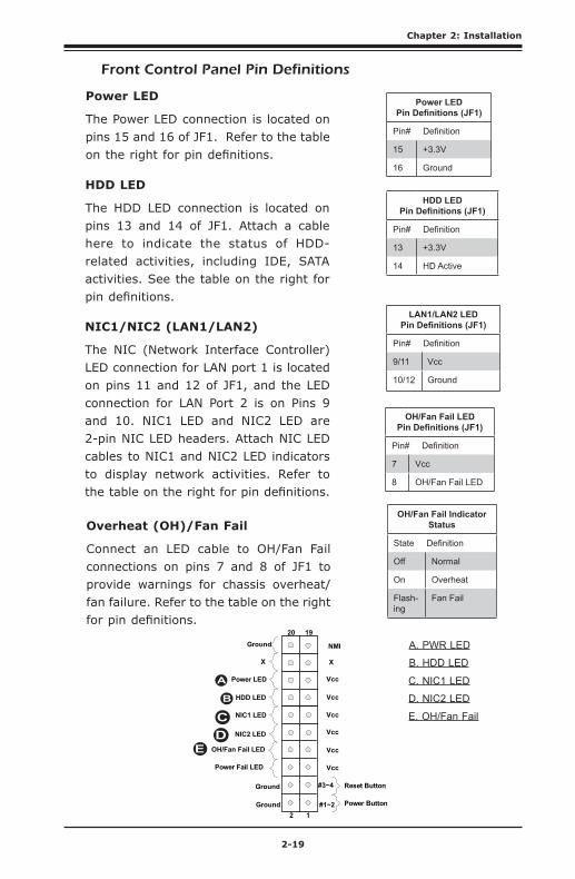
Chapter 2: Installation
2-19
Power Button
OH/Fan Fail LED
1
NIC1 LED
Reset Button
2
Power Fail LED
HDD LED
Power LED
#3~4
#1~2
Vcc
Vcc
Vcc
Vcc
Ground
Ground
1920
Vcc
X
Ground NMI
X
VccNIC2 LED
Front Control Panel Pin Definitions
Power LED
The Power LED connection is located on pins 15 and 16 of JF1. Refer to the table on the right for pin definitions.
Power LEDPin Definitions (JF1)
Pin# Definition
15 +3.3V
16 Ground
A. PWR LED
B. HDD LEDA
B
HDD LED
The HDD LED connection is located on pins 13 and 14 of JF1. Attach a cable here to indicate the status of HDD-related activities, including IDE, SATA activities. See the table on the right for pin definitions.
HDD LEDPin Definitions (JF1)
Pin# Definition
13 +3.3V
14 HD Active
NIC1/NIC2 (LAN1/LAN2)
The NIC (Network Interface Controller) LED connection for LAN port 1 is located on pins 11 and 12 of JF1, and the LED connection for LAN Port 2 is on Pins 9 and 10. NIC1 LED and NIC2 LED are 2-pin NIC LED headers. Attach NIC LED cables to NIC1 and NIC2 LED indicators to display network activities. Refer to the table on the right for pin definitions.
LAN1/LAN2 LEDPin Definitions (JF1)
Pin# Definition
9/11 Vcc
10/12 Ground
Overheat (OH)/Fan Fail
Connect an LED cable to OH/Fan Fail connections on pins 7 and 8 of JF1 to provide warnings for chassis overheat/fan failure. Refer to the table on the right for pin definitions.
OH/Fan Fail LEDPin Definitions (JF1)
Pin# Definition
7 Vcc
8 OH/Fan Fail LED
OH/Fan Fail Indicator Status
State Definition
Off Normal
On Overheat
Flash-ing
Fan Fail
C. NIC1 LED
D. NIC2 LED
E. OH/Fan FailCD
E
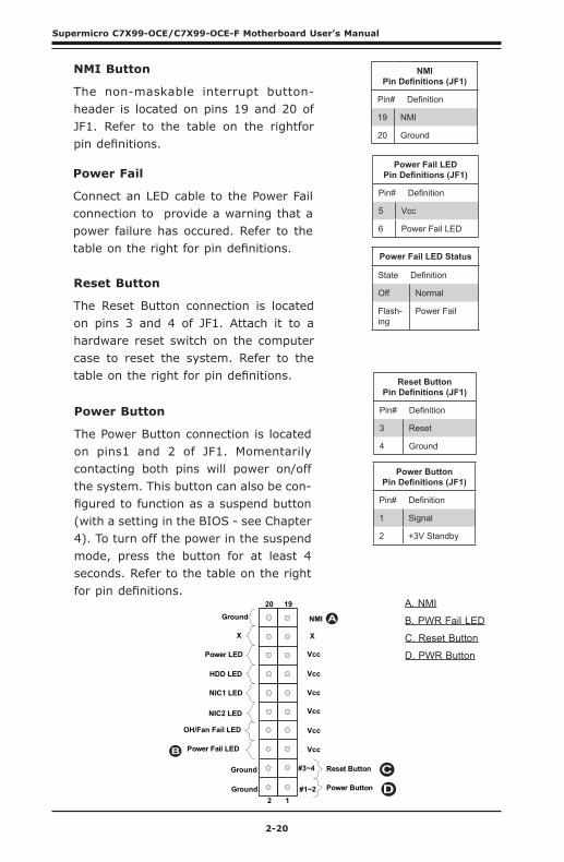
2-20
Supermicro C7X99-OCE/C7X99-OCE-F Motherboard User’s Manual
Power Button
The Power Button connection is located on pins1 and 2 of JF1. Momentarily contacting both pins will power on/off the system. This button can also be con-figured to function as a suspend button (with a setting in the BIOS - see Chapter 4). To turn off the power in the suspend mode, press the button for at least 4 seconds. Refer to the table on the right for pin definitions.
Power ButtonPin Definitions (JF1)
Pin# Definition
1 Signal
2 +3V Standby
Reset Button
The Reset Button connection is located on pins 3 and 4 of JF1. Attach it to a hardware reset switch on the computer case to reset the system. Refer to the table on the right for pin definitions. Reset Button
Pin Definitions (JF1)
Pin# Definition
3 Reset
4 Ground
A. NMI
B. PWR Fail LED
C. Reset Button
D. PWR Button
Power Button
OH/Fan Fail LED
1
NIC1 LED
Reset Button
2
Power Fail LED
HDD LED
Power LED
#3~4
#1~2
Vcc
Vcc
Vcc
Vcc
Ground
Ground
1920
Vcc
X
Ground NMI
X
VccNIC2 LED
A
B
CD
NMI Button
The non-maskable interrupt button-header is located on pins 19 and 20 of JF1. Refer to the table on the rightfor pin definitions.
Power Fail
Connect an LED cable to the Power Fail connection to provide a warning that a power failure has occured. Refer to the table on the right for pin definitions.
Power Fail LEDPin Definitions (JF1)
Pin# Definition
5 Vcc
6 Power Fail LED
Power Fail LED Status
State Definition
Off Normal
Flash-ing
Power Fail
NMIPin Definitions (JF1)
Pin# Definition
19 NMI
20 Ground
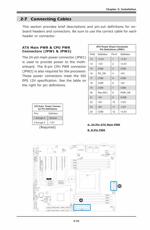
Chapter 2: Installation
2-21
MAC CODE
IPMI CODE
BAR CODEC7X99-OCE-F
SW_BIOSRC
S4
S7
S10
S5
S6
S9
OC_FRO
NT_PAN
EL
S8
S11
CLR_CMO
S_SW
JUSB30_I2
JAUD
IO1
LED4
I-SATA0I-SATA2I-SATA4S-SATA0S-SATA2
AUDIO_FP
JIPMB1
JSD1
MH11
MH
2
MH9
MH10
JPW2
C A
LEDM1
JBT1
BT1
+
FAN5
FAN4
FAN1
1
FAN2
4FAN3
JPL2
JPUSB1
J29J30
JPME2
JPAC1
JPL1
JI2C1JI2C2
JPB1
JPG1
JWD
11
JL2
JL1
JD1
1JF1
2
19
JPI2C1
JSTBY1
JTPM1
SP1
+
HD AUDIO
VGALAN1LAN2
USB 16/17(3.0)
USB 12/13(3.0) USB 10/11(3.0)USB 14/15(3.0)
CPU SLOT6 PCI-E 3.0 X16
PCH SLOT5 PCI-E 2.0 X1 (IN X4)
CPU SLOT4 PCI-E 3.0 X8 (IN X16)
PCH SLOT3 PCI-E 2.0 X1 (IN X4)
CPU SLOT2 PCI-E 3.0 X8 (IN X16)
CPU SLOT1 PCI-E 3.0 X8 (IN X16)
2-3:DISABLE
1-2:ENABLE
:WATCH
DO
G
SPEAKERPW
R LED
:TPM/PO
RT80
CPU
CHASSIS INTRUSION
JI2C2
2-3:DISABLE
1-2:ENABLE
JI2C1
PWR O
NO
H/FF
NIC1
NIC2
RSTX
CMO
S CLEAR
1-2:NORMAL2-3:BIOS RECOVERY
JBR1
PWR LED
HD
D LED
NM
IX
2-3:ME M
ANU
FACTURIN
G M
OD
E
JPME2
1-2:NO
RMAL
1-2 ENABLE2-3 DISABLE
1-2 ENABLE2-3 DISABLE
:PWR I2C
1-2 ENABLE
2-3 DISABLE
2-3 DISABLE
1-2 ENABLE
1-2 ENABLE2-3 DISABLE
JPAC1
VGA
USB14/15 WAKE UP
1-2 RST2-3 N
MI
:SATA DOM POWER
DIMMD2
DIMMD1
DIMMC2
DIMMC1
DIMMB2
DIMMB1
DIMMA2
DIMMA1
JBR1
JWD
1
JPW1
JPUSB1
JPB1JPG
1
C
A
LED1
I-SATA1I-SATA3I-SATA5S-SATA1S-SATA3
C7X99-OCE/
COM1
2-7 Connecting Cables
This section provides brief descriptions and pin-out definitions for on-board headers and connectors. Be sure to use the correct cable for each header or connector.
A. 24-Pin ATX Main PWR
B. 8-Pin PWR
ATX Power 24-pin ConnectorPin Definitions (JPW1)
Pin# Definition Pin # Definition
13 +3.3V 1 +3.3V
14 -12V 2 +3.3V
15 COM 3 COM
16 PS_ON 4 +5V
17 COM 5 COM
18 COM 6 +5V
19 COM 7 COM
20 Res (NC) 8 PWR_OK
21 +5V 9 5VSB
22 +5V 10 +12V
23 +5V 11 +12V
24 COM 12 +3.3V
(Required)
12V 8-pin Power Connec-tor Pin Definitions
Pins Definition
1 through 4 Ground
5 through 8 +12V
ATX Main PWR & CPU PWR Connectors (JPW1 & JPW2)
The 24-pin main power connector (JPW1) is used to provide power to the moth-erboard. The 8-pin CPU PWR connector (JPW2) is also required for the processor. These power connectors meet the SSI EPS 12V specification. See the table on the right for pin definitions.
A
B
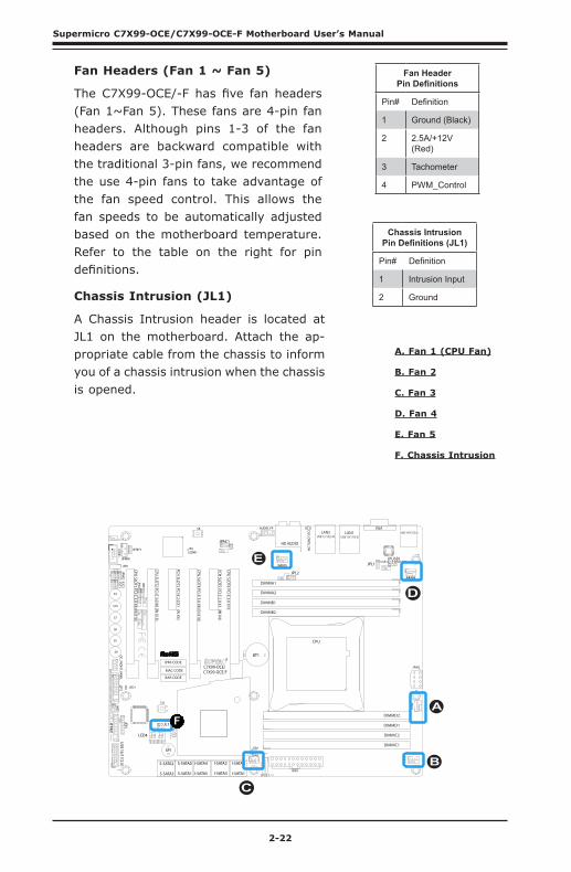
2-22
Supermicro C7X99-OCE/C7X99-OCE-F Motherboard User’s Manual
MAC CODE
IPMI CODE
BAR CODEC7X99-OCE-F
SW_BIOSRC
S4
S7
S10
S5
S6
S9
OC_FRO
NT_PAN
EL
S8
S11
CLR_CMO
S_SW
JUSB30_I2
JAUD
IO1
LED4
I-SATA0I-SATA2I-SATA4S-SATA0S-SATA2
AUDIO_FP
JIPMB1
JSD1
MH11
MH
2
MH9
MH10
JPW2
C A
LEDM1
JBT1
BT1
+
FAN5
FAN4
FAN1
1
FAN2
4FAN3
JPL2
JPUSB1
J29J30
JPME2
JPAC1
JPL1
JI2C1JI2C2
JPB1
JPG1
JWD
11
JL2
JL1
JD1
1JF1
2
19
JPI2C1
JSTBY1
JTPM1
SP1
+
HD AUDIO
VGALAN1LAN2
USB 16/17(3.0)
USB 12/13(3.0) USB 10/11(3.0)USB 14/15(3.0)
CPU SLOT6 PCI-E 3.0 X16
PCH SLOT5 PCI-E 2.0 X1 (IN X4)
CPU SLOT4 PCI-E 3.0 X8 (IN X16)
PCH SLOT3 PCI-E 2.0 X1 (IN X4)
CPU SLOT2 PCI-E 3.0 X8 (IN X16)
CPU SLOT1 PCI-E 3.0 X8 (IN X16)
2-3:DISABLE
1-2:ENABLE
:WATCH
DO
G
SPEAKERPW
R LED
:TPM/PO
RT80
CPU
CHASSIS INTRUSION
JI2C2
2-3:DISABLE
1-2:ENABLE
JI2C1
PWR O
NO
H/FF
NIC1
NIC2
RSTX
CMO
S CLEAR
1-2:NORMAL2-3:BIOS RECOVERY
JBR1
PWR LED
HD
D LED
NM
IX
2-3:ME M
ANU
FACTURIN
G M
OD
E
JPME2
1-2:NO
RMAL
1-2 ENABLE2-3 DISABLE
1-2 ENABLE2-3 DISABLE
:PWR I2C
1-2 ENABLE
2-3 DISABLE
2-3 DISABLE
1-2 ENABLE
1-2 ENABLE2-3 DISABLE
JPAC1
VGA
USB14/15 WAKE UP
1-2 RST2-3 N
MI
:SATA DOM POWER
DIMMD2
DIMMD1
DIMMC2
DIMMC1
DIMMB2
DIMMB1
DIMMA2
DIMMA1
JBR1
JWD
1
JPW1
JPUSB1
JPB1JPG
1
C
A
LED1
I-SATA1I-SATA3I-SATA5S-SATA1S-SATA3
C7X99-OCE/
COM1
Fan HeaderPin Definitions
Pin# Definition
1 Ground (Black)
2 2.5A/+12V (Red)
3 Tachometer
4 PWM_Control
Fan Headers (Fan 1 ~ Fan 5)
The C7X99-OCE/-F has five fan headers (Fan 1~Fan 5). These fans are 4-pin fan headers. Although pins 1-3 of the fan headers are backward compatible with the traditional 3-pin fans, we recommend the use 4-pin fans to take advantage of the fan speed control. This allows the fan speeds to be automatically adjusted based on the motherboard temperature. Refer to the table on the right for pin definitions.
A
B
A. Fan 1 (CPU Fan)
B. Fan 2
C. Fan 3
D. Fan 4
E. Fan 5
F. Chassis Intrusion
C
D
E
Chassis Intrusion (JL1)
A Chassis Intrusion header is located at JL1 on the motherboard. Attach the ap-propriate cable from the chassis to inform you of a chassis intrusion when the chassis is opened.
Chassis IntrusionPin Definitions (JL1)
Pin# Definition
1 Intrusion Input
2 Ground
F
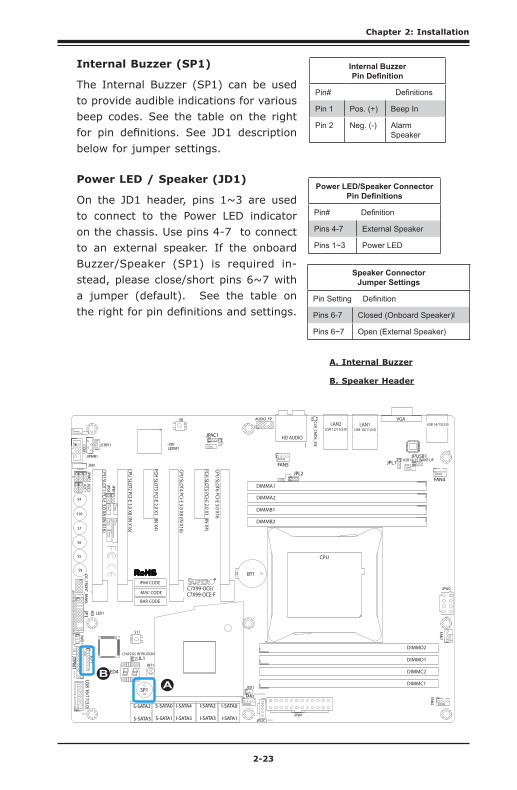
Chapter 2: Installation
2-23
Internal Buzzer (SP1)
The Internal Buzzer (SP1) can be used to provide audible indications for various beep codes. See the table on the right for pin definitions. See JD1 description below for jumper settings.
A. Internal Buzzer
B. Speaker Header
Internal BuzzerPin Definition
Pin# Definitions
Pin 1 Pos. (+) Beep In
Pin 2 Neg. (-) Alarm Speaker
Power LED / Speaker (JD1)
On the JD1 header, pins 1~3 are used to connect to the Power LED indicator on the chassis. Use pins 4-7 to connect to an external speaker. If the onboard Buzzer/Speaker (SP1) is required in-stead, please close/short pins 6~7 with a jumper (default). See the table on the right for pin definitions and settings.
Power LED/Speaker ConnectorPin Definitions
Pin# Definition
Pins 4-7 External Speaker
Pins 1~3 Power LED
MAC CODE
IPMI CODE
BAR CODEC7X99-OCE-F
SW_BIOSRC
S4
S7
S10
S5
S6
S9
OC_FRO
NT_PAN
EL
S8
S11
CLR_CMO
S_SW
JUSB30_I2
JAUD
IO1
LED4
I-SATA0I-SATA2I-SATA4S-SATA0S-SATA2
AUDIO_FP
JIPMB1
JSD1
MH11
MH
2
MH9
MH10
JPW2
C A
LEDM1
JBT1
BT1
+
FAN5
FAN4
FAN1
1
FAN2
4FAN3
JPL2
JPUSB1
J29J30
JPME2
JPAC1
JPL1
JI2C1JI2C2
JPB1
JPG1
JWD
11
JL2
JL1
JD1
1JF1
2
19
JPI2C1
JSTBY1JTPM
1
SP1
+
HD AUDIO
VGALAN1LAN2
USB 16/17(3.0)USB 12/13(3.0) USB 10/11(3.0)
USB 14/15(3.0)
CPU SLOT6 PCI-E 3.0 X16
PCH SLOT5 PCI-E 2.0 X1 (IN X4)
CPU SLOT4 PCI-E 3.0 X8 (IN X16)
PCH SLOT3 PCI-E 2.0 X1 (IN X4)
CPU SLOT2 PCI-E 3.0 X8 (IN X16)
CPU SLOT1 PCI-E 3.0 X8 (IN X16)
2-3:DISABLE
1-2:ENABLE
:WATCH
DO
G
SPEAKERPW
R LED
:TPM/PO
RT80
CPU
CHASSIS INTRUSION
JI2C2
2-3:DISABLE
1-2:ENABLE
JI2C1
PWR O
NO
H/FF
NIC1
NIC2
RSTX
CMO
S CLEAR
1-2:NORMAL2-3:BIOS RECOVERY
JBR1
PWR LED
HD
D LED
NM
IX
2-3:ME M
ANU
FACTURIN
G M
OD
E
JPME2
1-2:NO
RMAL
1-2 ENABLE2-3 DISABLE
1-2 ENABLE2-3 DISABLE
:PWR I2C
1-2 ENABLE
2-3 DISABLE
2-3 DISABLE
1-2 ENABLE
1-2 ENABLE2-3 DISABLE
JPAC1
VGA
USB14/15 WAKE UP
1-2 RST2-3 N
MI
:SATA DOM POWER
DIMMD2
DIMMD1
DIMMC2
DIMMC1
DIMMB2
DIMMB1
DIMMA2
DIMMA1
JBR1
JWD
1
JPW1
JPUSB1
JPB1JPG
1
C
A
LED1
I-SATA1I-SATA3I-SATA5S-SATA1S-SATA3
C7X99-OCE/
COM1
AB
Speaker ConnectorJumper Settings
Pin Setting Definition
Pins 6-7 Closed (Onboard Speaker)l
Pins 6~7 Open (External Speaker)
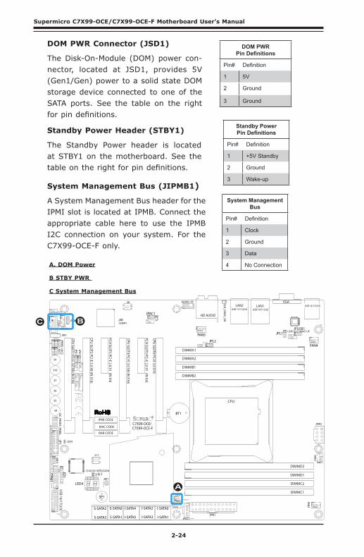
2-24
Supermicro C7X99-OCE/C7X99-OCE-F Motherboard User’s Manual
DOM PWR Connector (JSD1)
The Disk-On-Module (DOM) power con-nector, located at JSD1, provides 5V (Gen1/Gen) power to a solid state DOM storage device connected to one of the SATA ports. See the table on the right for pin definitions.
DOM PWRPin Definitions
Pin# Definition
1 5V
2 Ground
3 Ground
MAC CODE
IPMI CODE
BAR CODEC7X99-OCE-F
SW_BIOSRC
S4
S7
S10
S5
S6
S9
OC_FRO
NT_PAN
ELS8
S11
CLR_CMO
S_SW
JUSB30_I2
JAUD
IO1
LED4
I-SATA0I-SATA2I-SATA4S-SATA0S-SATA2
AUDIO_FP
JIPMB1
JSD1
MH11
MH
2
MH9
MH10
JPW2
C A
LEDM1
JBT1
BT1
+
FAN5
FAN4
FAN1
1
FAN2
4FAN3
JPL2
JPUSB1
J29J30
JPME2
JPAC1
JPL1
JI2C1JI2C2
JPB1
JPG1
JWD
11
JL2
JL1
JD1
1JF1
2
19
JPI2C1
JSTBY1
JTPM1
SP1
+
HD AUDIO
VGALAN1LAN2
USB 16/17(3.0)USB 12/13(3.0) USB 10/11(3.0)
USB 14/15(3.0)
CPU SLOT6 PCI-E 3.0 X16
PCH SLOT5 PCI-E 2.0 X1 (IN X4)
CPU SLOT4 PCI-E 3.0 X8 (IN X16)
PCH SLOT3 PCI-E 2.0 X1 (IN X4)
CPU SLOT2 PCI-E 3.0 X8 (IN X16)
CPU SLOT1 PCI-E 3.0 X8 (IN X16)
2-3:DISABLE
1-2:ENABLE
:WATCH
DO
G
SPEAKERPW
R LED
:TPM/PO
RT80
CPU
CHASSIS INTRUSION
JI2C2
2-3:DISABLE
1-2:ENABLE
JI2C1
PWR O
NO
H/FF
NIC1
NIC2
RSTX
CMO
S CLEAR
1-2:NORMAL2-3:BIOS RECOVERY
JBR1
PWR LED
HD
D LED
NM
IX
2-3:ME M
ANU
FACTURIN
G M
OD
E
JPME2
1-2:NO
RMAL
1-2 ENABLE2-3 DISABLE
1-2 ENABLE2-3 DISABLE
:PWR I2C
1-2 ENABLE
2-3 DISABLE
2-3 DISABLE
1-2 ENABLE
1-2 ENABLE2-3 DISABLE
JPAC1
VGA
USB14/15 WAKE UP
1-2 RST2-3 N
MI
:SATA DOM POWER
DIMMD2
DIMMD1
DIMMC2
DIMMC1
DIMMB2
DIMMB1
DIMMA2
DIMMA1
JBR1
JWD
1
JPW1
JPUSB1
JPB1JPG
1
C
A
LED1
I-SATA1I-SATA3I-SATA5S-SATA1S-SATA3
C7X99-OCE/
COM1
A
B
A. DOM Power
B STBY PWR
C System Management Bus
Standby Power Header (STBY1)
The Standby Power header is located at STBY1 on the motherboard. See the table on the right for pin definitions.
Standby PowerPin Definitions
Pin# Definition
1 +5V Standby
2 Ground
3 Wake-upSystem Management Bus (JIPMB1)
A System Management Bus header for the IPMI slot is located at IPMB. Connect the appropriate cable here to use the IPMB I2C connection on your system. For the C7X99-OCE-F only.
System Management Bus
Pin# Definition
1 Clock
2 Ground
3 Data
4 No Connection
C
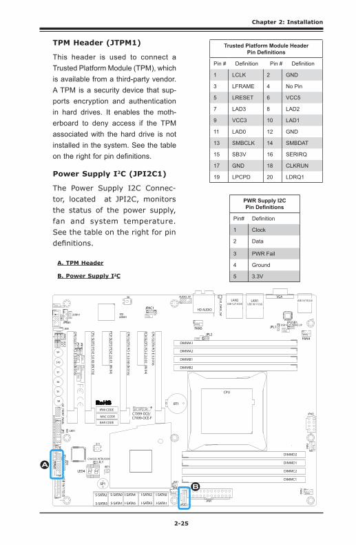
Chapter 2: Installation
2-25
MAC CODE
IPMI CODE
BAR CODEC7X99-OCE-F
SW_BIOSRC
S4
S7
S10
S5
S6
S9
OC_FRO
NT_PAN
ELS8
S11
CLR_CMO
S_SW
JUSB30_I2
JAUD
IO1
LED4
I-SATA0I-SATA2I-SATA4S-SATA0S-SATA2
AUDIO_FP
JIPMB1
JSD1
MH11
MH
2
MH9
MH10
JPW2
C A
LEDM1
JBT1
BT1
+
FAN5
FAN4
FAN1
1
FAN2
4FAN3
JPL2
JPUSB1
J29J30
JPME2
JPAC1
JPL1
JI2C1JI2C2
JPB1
JPG1
JWD
11
JL2
JL1
JD1
1JF1
2
19
JPI2C1
JSTBY1
JTPM1
SP1
+
HD AUDIO
VGALAN1LAN2
USB 16/17(3.0)
USB 12/13(3.0) USB 10/11(3.0)USB 14/15(3.0)
CPU SLOT6 PCI-E 3.0 X16
PCH SLOT5 PCI-E 2.0 X1 (IN X4)
CPU SLOT4 PCI-E 3.0 X8 (IN X16)
PCH SLOT3 PCI-E 2.0 X1 (IN X4)
CPU SLOT2 PCI-E 3.0 X8 (IN X16)
CPU SLOT1 PCI-E 3.0 X8 (IN X16)
2-3:DISABLE
1-2:ENABLE
:WATCH
DO
G
SPEAKERPW
R LED
:TPM/PO
RT80
CPU
CHASSIS INTRUSION
JI2C2
2-3:DISABLE
1-2:ENABLE
JI2C1
PWR O
NO
H/FF
NIC1
NIC2
RSTX
CMO
S CLEAR
1-2:NORMAL2-3:BIOS RECOVERY
JBR1
PWR LED
HD
D LED
NM
IX
2-3:ME M
ANU
FACTURIN
G M
OD
E
JPME2
1-2:NO
RMAL
1-2 ENABLE2-3 DISABLE
1-2 ENABLE2-3 DISABLE
:PWR I2C
1-2 ENABLE
2-3 DISABLE
2-3 DISABLE
1-2 ENABLE
1-2 ENABLE2-3 DISABLE
JPAC1
VGA
USB14/15 WAKE UP
1-2 RST2-3 N
MI
:SATA DOM POWER
DIMMD2
DIMMD1
DIMMC2
DIMMC1
DIMMB2
DIMMB1
DIMMA2
DIMMA1
JBR1
JWD
1
JPW1
JPUSB1
JPB1JPG
1
C
A
LED1
I-SATA1I-SATA3I-SATA5S-SATA1S-SATA3
C7X99-OCE/
COM1
Trusted Platform Module HeaderPin Definitions
Pin # Definition Pin # Definition
1 LCLK 2 GND
3 LFRAME 4 No Pin
5 LRESET 6 VCC5
7 LAD3 8 LAD2
9 VCC3 10 LAD1
11 LAD0 12 GND
13 SMBCLK 14 SMBDAT
15 SB3V 16 SERIRQ
17 GND 18 CLKRUN
19 LPCPD 20 LDRQ1
TPM Header (JTPM1)
This header is used to connect a Trusted Platform Module (TPM), which is available from a third-party vendor. A TPM is a security device that sup-ports encryption and authentication in hard drives. It enables the moth-erboard to deny access if the TPM associated with the hard drive is not installed in the system. See the table on the right for pin definitions.
Power Supply I2C (JPI2C1)
The Power Supply I2C Connec-tor, located at JPI2C, monitors the status of the power supply, fan and system temperature. See the table on the right for pin definitions.
PWR Supply I2CPin Definitions
Pin# Definition
1 Clock
2 Data
3 PWR Fail
4 Ground
5 3.3V
A
B
A. TPM Header
B. Power Supply I2C
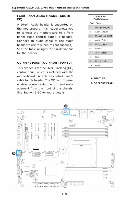
2-26
Supermicro C7X99-OCE/C7X99-OCE-F Motherboard User’s Manual
MAC CODE
IPMI CODE
BAR CODEC7X99-OCE-F
SW_BIOSRC
S4
S7
S10
S5
S6
S9
OC_FRO
NT_PAN
ELS8
S11
CLR_CMO
S_SW
JUSB30_I2
JAUD
IO1
LED4
I-SATA0I-SATA2I-SATA4S-SATA0S-SATA2
AUDIO_FP
JIPMB1
JSD1
MH11
MH
2
MH9
MH10
JPW2
C A
LEDM1
JBT1
BT1
+
FAN5
FAN4
FAN1
1
FAN2
4FAN3
JPL2
JPUSB1
J29J30
JPME2
JPAC1
JPL1
JI2C1JI2C2
JPB1
JPG1
JWD
11
JL2
JL1
JD1
1JF1
2
19
JPI2C1
JSTBY1
JTPM1
SP1
+
HD AUDIO
VGALAN1LAN2
USB 16/17(3.0)USB 12/13(3.0) USB 10/11(3.0)
USB 14/15(3.0)
CPU SLOT6 PCI-E 3.0 X16
PCH SLOT5 PCI-E 2.0 X1 (IN X4)
CPU SLOT4 PCI-E 3.0 X8 (IN X16)
PCH SLOT3 PCI-E 2.0 X1 (IN X4)
CPU SLOT2 PCI-E 3.0 X8 (IN X16)
CPU SLOT1 PCI-E 3.0 X8 (IN X16)
2-3:DISABLE
1-2:ENABLE
:WATCH
DO
G
SPEAKERPW
R LED
:TPM/PO
RT80
CPU
CHASSIS INTRUSION
JI2C2
2-3:DISABLE
1-2:ENABLE
JI2C1
PWR O
NO
H/FF
NIC1
NIC2
RSTX
CMO
S CLEAR
1-2:NORMAL2-3:BIOS RECOVERY
JBR1
PWR LED
HD
D LED
NM
IX
2-3:ME M
ANU
FACTURIN
G M
OD
E
JPME2
1-2:NO
RMAL
1-2 ENABLE2-3 DISABLE
1-2 ENABLE2-3 DISABLE
:PWR I2C
1-2 ENABLE
2-3 DISABLE
2-3 DISABLE
1-2 ENABLE
1-2 ENABLE2-3 DISABLE
JPAC1
VGA
USB14/15 WAKE UP
1-2 RST2-3 N
MI
:SATA DOM POWER
DIMMD2
DIMMD1
DIMMC2
DIMMC1
DIMMB2
DIMMB1
DIMMA2
DIMMA1
JBR1
JWD
1
JPW1
JPUSB1
JPB1JPG
1
C
A
LED1
I-SATA1I-SATA3I-SATA5S-SATA1S-SATA3
C7X99-OCE/
COM1
A. AUDIO FP
B. OC FRONT PANEL
A
Front Panel Audio Header (AUDIO FP)
A 10-pin Audio header is supported on the motherboard. This header allows you to connect the motherboard to a front panel audio control panet, if needed. Connect an audio cable to the audio header to use this feature (not supplied). See the table at right for pin definitions for the header.
10-in AudioPin Definitions
Pin# Signal
1 Microphone_Left
2 Audio_Ground
3 Microphone_Right
4 Audio_Detect
5 Line_2_Right
6 Ground
7 Jack_Detect
8 Key
9 Line_2_Left
10 GroundOC Front Panel (OC FRONT PANEL)
This header is for the Over-Clocking (OC) control panel which is included with the motherboard. Attach the control panel's cable to this header. The OC control panel enables over-clocking control and man-agement from the front of the chassis. See Section 2-10 for more details.
B
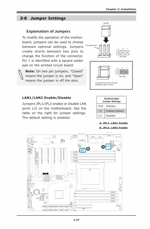
Chapter 2: Installation
2-27
2-8 Jumper Settings
Explanation of Jumpers
To modify the operation of the mother-board, jumpers can be used to choose between optional settings. Jumpers create shorts between two pins to change the function of the connector. Pin 1 is identified with a square solder pad on the printed circuit board.
Note: On two pin jumpers, "Closed" means the jumper is on, and "Open" means the jumper is off the pins.
A. JPL1: LAN1 Enable
B. JPL2: LAN2 Enable
LAN1/LAN2 Enable/Disable
Jumpers JPL1/JPL2 enable or disable LAN ports 1/2 on the motherboard. See the table on the right for jumper settings. The default setting is enabled.
GLAN EnableJumper Settings
Pin# Definition
1-2 Enabled (default)
2-3 Disabled
MAC CODE
IPMI CODE
BAR CODEC7X99-OCE-F
SW_BIOSRC
S4
S7
S10
S5
S6
S9
OC_FRO
NT_PAN
EL
S8
S11
CLR_CMO
S_SW
JUSB30_I2
JAUD
IO1
LED4
I-SATA0I-SATA2I-SATA4S-SATA0S-SATA2
AUDIO_FP
JIPMB1
JSD1
MH11
MH
2
MH9
MH10
JPW2
C A
LEDM1
JBT1
BT1
+
FAN5
FAN4
FAN1
1
FAN2
4FAN3
JPL2
JPUSB1
J29J30
JPME2
JPAC1
JPL1
JI2C1JI2C2
JPB1
JPG1
JWD
11
JL2
JL1
JD1
1JF1
2
19
JPI2C1
JSTBY1
JTPM1
SP1
+
HD AUDIO
VGALAN1LAN2
USB 16/17(3.0)
USB 12/13(3.0) USB 10/11(3.0)USB 14/15(3.0)
CPU SLOT6 PCI-E 3.0 X16
PCH SLOT5 PCI-E 2.0 X1 (IN X4)
CPU SLOT4 PCI-E 3.0 X8 (IN X16)
PCH SLOT3 PCI-E 2.0 X1 (IN X4)
CPU SLOT2 PCI-E 3.0 X8 (IN X16)
CPU SLOT1 PCI-E 3.0 X8 (IN X16)
2-3:DISABLE
1-2:ENABLE
:WATCH
DO
G
SPEAKERPW
R LED
:TPM/PO
RT80
CPU
CHASSIS INTRUSION
JI2C2
2-3:DISABLE
1-2:ENABLE
JI2C1
PWR O
NO
H/FF
NIC1
NIC2
RSTX
CMO
S CLEAR
1-2:NORMAL2-3:BIOS RECOVERY
JBR1
PWR LED
HD
D LED
NM
IX
2-3:ME M
ANU
FACTURIN
G M
OD
E
JPME2
1-2:NO
RMAL
1-2 ENABLE2-3 DISABLE
1-2 ENABLE2-3 DISABLE
:PWR I2C
1-2 ENABLE
2-3 DISABLE
2-3 DISABLE
1-2 ENABLE
1-2 ENABLE2-3 DISABLE
JPAC1
VGA
USB14/15 WAKE UP
1-2 RST2-3 N
MI
:SATA DOM POWER
DIMMD2
DIMMD1
DIMMC2
DIMMC1
DIMMB2
DIMMB1
DIMMA2
DIMMA1
JBR1
JWD
1
JPW1
JPUSB1
JPB1JPG
1
C
A
LED1
I-SATA1I-SATA3I-SATA5S-SATA1S-SATA3
C7X99-OCE/
COM1
AB
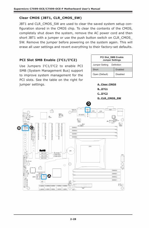
2-28
Supermicro C7X99-OCE/C7X99-OCE-F Motherboard User’s Manual
Clear CMOS (JBT1, CLR_CMOS_SW)
JBT1 and CLR_CMOS_SW are used to clear the saved system setup con-figuration stored in the CMOS chip. To clear the contents of the CMOS, completely shut down the system, remove the AC power cord and then short JBT1 with a jumper or use the push button switch on CLR_CMOS_SW. Remove the jumper before powering on the system again. This will erase all user settings and revert everything to their factory-set defaults.
A. Clear CMOS
B. JI2C1
C. JI2C2
D. CLR_CMOS_SW
PCI Slot_SMB EnableJumper Settings
Jumper Setting Definition
Short Enabled
Open (Default) Disabled
PCI Slot SMB Enable (I2C1/I2C2)
Use Jumpers I2C1/I2C2 to enable PCI SMB (System Management Bus) support to improve system management for the PCI slots. See the table on the right for jumper settings.
MAC CODE
IPMI CODE
BAR CODEC7X99-OCE-F
SW_BIOSRC
S4
S7
S10
S5
S6
S9
OC_FRO
NT_PAN
EL
S8
S11
CLR_CMO
S_SW
JUSB30_I2
JAUD
IO1
LED4
I-SATA0I-SATA2I-SATA4S-SATA0S-SATA2
AUDIO_FP
JIPMB1
JSD1
MH11
MH
2
MH9
MH10
JPW2
C A
LEDM1
JBT1
BT1
+
FAN5
FAN4
FAN1
1
FAN2
4FAN3
JPL2
JPUSB1
J29J30
JPME2
JPAC1
JPL1JI2C1JI2C2
JPB1
JPG1
JWD
11
JL2
JL1
JD1
1JF1
2
19
JPI2C1
JSTBY1
JTPM1
SP1
+
HD AUDIO
VGALAN1LAN2
USB 16/17(3.0)
USB 12/13(3.0) USB 10/11(3.0)USB 14/15(3.0)
CPU SLOT6 PCI-E 3.0 X16
PCH SLOT5 PCI-E 2.0 X1 (IN X4)
CPU SLOT4 PCI-E 3.0 X8 (IN X16)
PCH SLOT3 PCI-E 2.0 X1 (IN X4)
CPU SLOT2 PCI-E 3.0 X8 (IN X16)
CPU SLOT1 PCI-E 3.0 X8 (IN X16)
2-3:DISABLE
1-2:ENABLE
:WATCH
DO
G
SPEAKERPW
R LED
:TPM/PO
RT80
CPU
CHASSIS INTRUSION
JI2C2
2-3:DISABLE
1-2:ENABLE
JI2C1
PWR O
NO
H/FF
NIC1
NIC2
RSTX
CMO
S CLEAR
1-2:NORMAL2-3:BIOS RECOVERY
JBR1
PWR LED
HD
D LED
NM
IX
2-3:ME M
ANU
FACTURIN
G M
OD
E
JPME2
1-2:NO
RMAL
1-2 ENABLE2-3 DISABLE
1-2 ENABLE2-3 DISABLE
:PWR I2C
1-2 ENABLE
2-3 DISABLE
2-3 DISABLE
1-2 ENABLE
1-2 ENABLE2-3 DISABLE
JPAC1
VGA
USB14/15 WAKE UP
1-2 RST2-3 N
MI
:SATA DOM POWER
DIMMD2
DIMMD1
DIMMC2
DIMMC1
DIMMB2
DIMMB1
DIMMA2
DIMMA1
JBR1JW
D1
JPW1
JPUSB1
JPB1JPG
1
C
A
LED1
I-SATA1I-SATA3I-SATA5S-SATA1S-SATA3
C7X99-OCE/
COM1
C
A
B
D
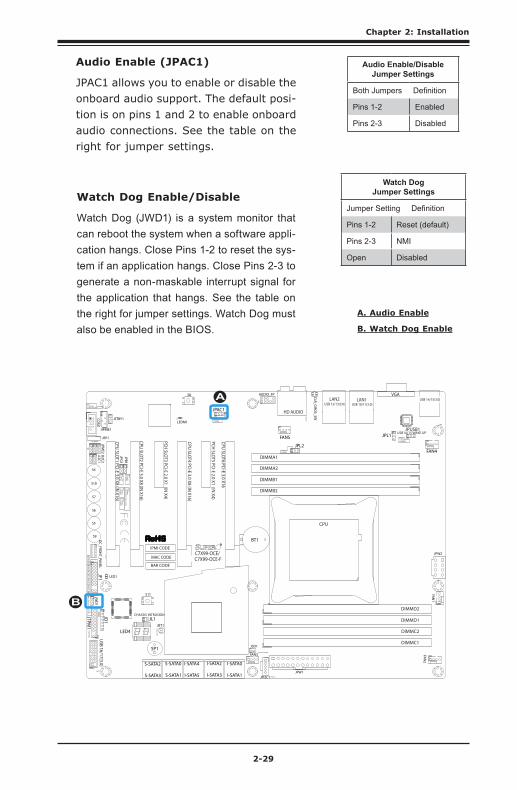
Chapter 2: Installation
2-29
A. Audio Enable
B. Watch Dog Enable
Audio Enable/Disable Jumper Settings
Both Jumpers Definition
Pins 1-2 Enabled
Pins 2-3 Disabled
Audio Enable (JPAC1)
JPAC1 allows you to enable or disable the onboard audio support. The default posi-tion is on pins 1 and 2 to enable onboard audio connections. See the table on the right for jumper settings.
MAC CODE
IPMI CODE
BAR CODEC7X99-OCE-F
SW_BIOSRC
S4
S7
S10
S5
S6
S9
OC_FRO
NT_PAN
EL
S8
S11
CLR_CMO
S_SW
JUSB30_I2
JAUD
IO1
LED4
I-SATA0I-SATA2I-SATA4S-SATA0S-SATA2
AUDIO_FP
JIPMB1
JSD1
MH11
MH
2
MH9
MH10
JPW2
C A
LEDM1
JBT1
BT1
+
FAN5
FAN4
FAN1
1
FAN2
4FAN3
JPL2
JPUSB1
J29J30
JPME2
JPAC1
JPL1
JI2C1JI2C2
JPB1
JPG1
JWD
11
JL2
JL1
JD1
1JF1
2
19
JPI2C1
JSTBY1
JTPM1
SP1
+
HD AUDIO
VGALAN1LAN2
USB 16/17(3.0)
USB 12/13(3.0) USB 10/11(3.0)USB 14/15(3.0)
CPU SLOT6 PCI-E 3.0 X16
PCH SLOT5 PCI-E 2.0 X1 (IN X4)
CPU SLOT4 PCI-E 3.0 X8 (IN X16)
PCH SLOT3 PCI-E 2.0 X1 (IN X4)
CPU SLOT2 PCI-E 3.0 X8 (IN X16)
CPU SLOT1 PCI-E 3.0 X8 (IN X16)
2-3:DISABLE
1-2:ENABLE
:WATCH
DO
G
SPEAKERPW
R LED
:TPM/PO
RT80
CPU
CHASSIS INTRUSION
JI2C2
2-3:DISABLE
1-2:ENABLE
JI2C1
PWR O
NO
H/FF
NIC1
NIC2
RSTX
CMO
S CLEAR
1-2:NORMAL2-3:BIOS RECOVERY
JBR1
PWR LED
HD
D LED
NM
IX
2-3:ME M
ANU
FACTURIN
G M
OD
E
JPME2
1-2:NO
RMAL
1-2 ENABLE2-3 DISABLE
1-2 ENABLE2-3 DISABLE
:PWR I2C
1-2 ENABLE
2-3 DISABLE
2-3 DISABLE
1-2 ENABLE
1-2 ENABLE2-3 DISABLE
JPAC1
VGA
USB14/15 WAKE UP
1-2 RST2-3 N
MI
:SATA DOM POWER
DIMMD2
DIMMD1
DIMMC2
DIMMC1
DIMMB2
DIMMB1
DIMMA2
DIMMA1
JBR1
JWD
1
JPW1
JPUSB1
JPB1JPG
1
C
A
LED1
I-SATA1I-SATA3I-SATA5S-SATA1S-SATA3
C7X99-OCE/
COM1
A
B
Watch Dog Enable/Disable
Watch Dog (JWD1) is a system monitor that can reboot the system when a software appli-cation hangs. Close Pins 1-2 to reset the sys-tem if an application hangs. Close Pins 2-3 to generate a non-maskable interrupt signal for the application that hangs. See the table on the right for jumper settings. Watch Dog must also be enabled in the BIOS.
Watch Dog Jumper Settings
Jumper Setting Definition
Pins 1-2 Reset (default)
Pins 2-3 NMI
Open Disabled
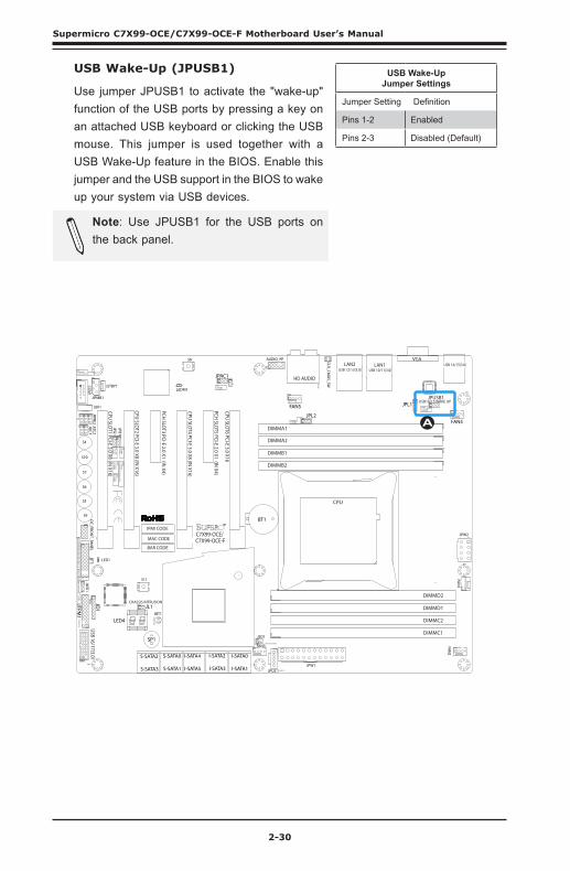
2-30
Supermicro C7X99-OCE/C7X99-OCE-F Motherboard User’s Manual
USB Wake-Up (JPUSB1)
Use jumper JPUSB1 to activate the "wake-up" function of the USB ports by pressing a key on an attached USB keyboard or clicking the USB mouse. This jumper is used together with a USB Wake-Up feature in the BIOS. Enable this jumper and the USB support in the BIOS to wake up your system via USB devices.
Note: Use JPUSB1 for the USB ports on the back panel.
MAC CODE
IPMI CODE
BAR CODEC7X99-OCE-F
SW_BIOSRC
S4
S7
S10
S5
S6
S9
OC_FRO
NT_PAN
EL
S8
S11
CLR_CMO
S_SW
JUSB30_I2
JAUD
IO1
LED4
I-SATA0I-SATA2I-SATA4S-SATA0S-SATA2
AUDIO_FP
JIPMB1
JSD1
MH11
MH
2
MH9
MH10
JPW2
C A
LEDM1
JBT1
BT1
+
FAN5
FAN4
FAN1
1
FAN2
4FAN3
JPL2
JPUSB1
J29J30
JPME2
JPAC1
JPL1
JI2C1JI2C2
JPB1
JPG1
JWD
11
JL2
JL1
JD1
1JF1
2
19
JPI2C1
JSTBY1
JTPM1
SP1
+
HD AUDIO
VGALAN1LAN2
USB 16/17(3.0)
USB 12/13(3.0) USB 10/11(3.0)USB 14/15(3.0)
CPU SLOT6 PCI-E 3.0 X16
PCH SLOT5 PCI-E 2.0 X1 (IN X4)
CPU SLOT4 PCI-E 3.0 X8 (IN X16)
PCH SLOT3 PCI-E 2.0 X1 (IN X4)
CPU SLOT2 PCI-E 3.0 X8 (IN X16)
CPU SLOT1 PCI-E 3.0 X8 (IN X16)
2-3:DISABLE
1-2:ENABLE
:WATCH
DO
G
SPEAKERPW
R LED
:TPM/PO
RT80
CPU
CHASSIS INTRUSION
JI2C2
2-3:DISABLE
1-2:ENABLE
JI2C1
PWR O
NO
H/FF
NIC1
NIC2
RSTX
CMO
S CLEAR
1-2:NORMAL2-3:BIOS RECOVERY
JBR1
PWR LED
HD
D LED
NM
IX
2-3:ME M
ANU
FACTURIN
G M
OD
E
JPME2
1-2:NO
RMAL
1-2 ENABLE2-3 DISABLE
1-2 ENABLE2-3 DISABLE
:PWR I2C
1-2 ENABLE
2-3 DISABLE
2-3 DISABLE
1-2 ENABLE
1-2 ENABLE2-3 DISABLE
JPAC1
VGA
USB14/15 WAKE UP
1-2 RST2-3 N
MI
:SATA DOM POWER
DIMMD2
DIMMD1
DIMMC2
DIMMC1
DIMMB2
DIMMB1
DIMMA2
DIMMA1
JBR1
JWD
1
JPW1
JPUSB1
JPB1JPG
1
C
A
LED1
I-SATA1I-SATA3I-SATA5S-SATA1S-SATA3
C7X99-OCE/
COM1
A
USB Wake-Up Jumper Settings
Jumper Setting Definition
Pins 1-2 Enabled
Pins 2-3 Disabled (Default)
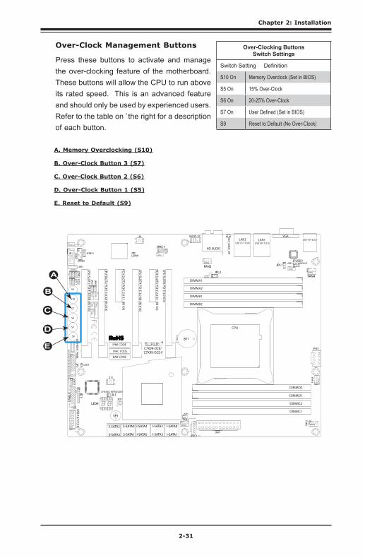
Chapter 2: Installation
2-31
Over-Clock Management Buttons
Press these buttons to activate and manage the over-clocking feature of the motherboard. These buttons will allow the CPU to run above its rated speed. This is an advanced feature and should only be used by experienced users. Refer to the table on `the right for a description of each button.
Over-Clocking Buttons Switch Settings
Switch Setting Definition
S10 On Memory Overclock (Set in BIOS)
S5 On 15% Over-Clock
S6 On 20-25% Over-Clock
S7 On User Defined (Set in BIOS)
S9 Reset to Default (No Over-Clock)
MAC CODE
IPMI CODE
BAR CODEC7X99-OCE-F
SW_BIOSRC
S4
S7
S10
S5
S6
S9
OC_FRO
NT_PAN
EL
S8
S11
CLR_CMO
S_SW
JUSB30_I2
JAUD
IO1
LED4
I-SATA0I-SATA2I-SATA4S-SATA0S-SATA2
AUDIO_FP
JIPMB1
JSD1
MH11
MH
2
MH9
MH10
JPW2
C A
LEDM1
JBT1
BT1
+
FAN5
FAN4
FAN1
1
FAN2
4FAN3
JPL2
JPUSB1
J29J30
JPME2
JPAC1
JPL1
JI2C1JI2C2
JPB1
JPG1
JWD
11
JL2
JL1
JD1
1JF1
2
19
JPI2C1
JSTBY1
JTPM1
SP1
+
HD AUDIO
VGALAN1LAN2
USB 16/17(3.0)
USB 12/13(3.0) USB 10/11(3.0)USB 14/15(3.0)
CPU SLOT6 PCI-E 3.0 X16
PCH SLOT5 PCI-E 2.0 X1 (IN X4)
CPU SLOT4 PCI-E 3.0 X8 (IN X16)
PCH SLOT3 PCI-E 2.0 X1 (IN X4)
CPU SLOT2 PCI-E 3.0 X8 (IN X16)
CPU SLOT1 PCI-E 3.0 X8 (IN X16)
2-3:DISABLE
1-2:ENABLE
:WATCH
DO
G
SPEAKERPW
R LED
:TPM/PO
RT80
CPU
CHASSIS INTRUSION
JI2C2
2-3:DISABLE
1-2:ENABLE
JI2C1
PWR O
NO
H/FF
NIC1
NIC2
RSTX
CMO
S CLEAR
1-2:NORMAL2-3:BIOS RECOVERY
JBR1
PWR LED
HD
D LED
NM
IX
2-3:ME M
ANU
FACTURIN
G M
OD
E
JPME2
1-2:NO
RMAL
1-2 ENABLE2-3 DISABLE
1-2 ENABLE2-3 DISABLE
:PWR I2C
1-2 ENABLE
2-3 DISABLE
2-3 DISABLE
1-2 ENABLE
1-2 ENABLE2-3 DISABLE
JPAC1
VGA
USB14/15 WAKE UP
1-2 RST2-3 N
MI
:SATA DOM POWER
DIMMD2
DIMMD1
DIMMC2
DIMMC1
DIMMB2
DIMMB1
DIMMA2
DIMMA1
JBR1
JWD
1
JPW1
JPUSB1
JPB1JPG
1
C
A
LED1
I-SATA1I-SATA3I-SATA5S-SATA1S-SATA3
C7X99-OCE/
COM1
A
B
C
D
E
A. Memory Overclocking (S10)
B. Over-Clock Button 3 (S7)
C. Over-Clock Button 2 (S6)
D. Over-Clock Button 1 (S5)
E. Reset to Default (S9)
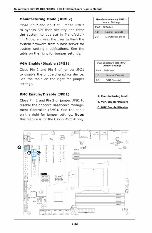
2-32
Supermicro C7X99-OCE/C7X99-OCE-F Motherboard User’s Manual
MAC CODE
IPMI CODE
BAR CODEC7X99-OCE-F
SW_BIOSRC
S4
S7
S10
S5
S6
S9
OC_FRO
NT_PAN
EL
S8
S11
CLR_CMO
S_SW
JUSB30_I2
JAUD
IO1
LED4
I-SATA0I-SATA2I-SATA4S-SATA0S-SATA2
AUDIO_FP
JIPMB1
JSD1
MH11
MH
2
MH9
MH10
JPW2
C A
LEDM1
JBT1
BT1
+
FAN5
FAN4
FAN1
1
FAN2
4FAN3
JPL2
JPUSB1
J29J30
JPME2
JPAC1
JPL1
JI2C1JI2C2
JPB1
JPG1
JWD
11
JL2
JL1
JD1
1JF1
2
19
JPI2C1
JSTBY1
JTPM1
SP1
+
HD AUDIO
VGALAN1LAN2
USB 16/17(3.0)
USB 12/13(3.0) USB 10/11(3.0)USB 14/15(3.0)
CPU SLOT6 PCI-E 3.0 X16
PCH SLOT5 PCI-E 2.0 X1 (IN X4)
CPU SLOT4 PCI-E 3.0 X8 (IN X16)
PCH SLOT3 PCI-E 2.0 X1 (IN X4)
CPU SLOT2 PCI-E 3.0 X8 (IN X16)
CPU SLOT1 PCI-E 3.0 X8 (IN X16)
2-3:DISABLE
1-2:ENABLE
:WATCH
DO
G
SPEAKERPW
R LED
:TPM/PO
RT80
CPU
CHASSIS INTRUSION
JI2C2
2-3:DISABLE
1-2:ENABLE
JI2C1
PWR O
NO
H/FF
NIC1
NIC2
RSTX
CMO
S CLEAR
1-2:NORMAL2-3:BIOS RECOVERY
JBR1
PWR LED
HD
D LED
NM
IX
2-3:ME M
ANU
FACTURIN
G M
OD
E
JPME2
1-2:NO
RMAL
1-2 ENABLE2-3 DISABLE
1-2 ENABLE2-3 DISABLE
:PWR I2C
1-2 ENABLE
2-3 DISABLE
2-3 DISABLE
1-2 ENABLE
1-2 ENABLE2-3 DISABLE
JPAC1
VGA
USB14/15 WAKE UP
1-2 RST2-3 N
MI
:SATA DOM POWER
DIMMD2
DIMMD1
DIMMC2
DIMMC1
DIMMB2
DIMMB1
DIMMA2
DIMMA1
JBR1
JWD
1
JPW1
JPUSB1
JPB1JPG
1
C
A
LED1
I-SATA1I-SATA3I-SATA5S-SATA1S-SATA3
C7X99-OCE/
COM1
B
A
Manufacturing Mode (JPME2)
Close Pin 2 and Pin 3 of Jumper JPME2 to bypass SPI flash security and force the system to operate in Manufactur-ing Mode, allowing the user to flash the system firmware from a host server for system setting modifications. See the table on the right for jumper settings.
Manufacture Mode (JPME2)Jumper Settings
Pin# Definition
1-2 Normal (Default)
2-3 Manufacture Mode
A. Manufacturing Mode
B. VGA Enable/Disable
C. BMC Enable/Disable
VGA Enable/Disable (JPG1)
Close Pin 2 and Pin 3 of jumper JPG1 to disable the onboard graphics device. See the table on the right for jumper settings.
VGA Enable/Disable (JPG1)Jumper Settings
Pin# Definition
1-2 Normal (Default)
2-3 VGA Disabled
BMC Enable/Disable (JPB1)
Close Pin 2 and Pin 3 of jumper JPB1 to disable the onboard Baseboard Manage-ment Controller (BMC). See the table on the right for jumper settings. Note: this feature is for the C7X99-OCE-F only.
C
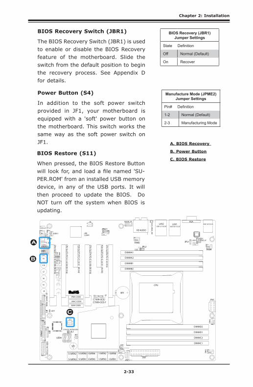
Chapter 2: Installation
2-33
MAC CODE
IPMI CODE
BAR CODEC7X99-OCE-F
SW_BIOSRC
S4
S7
S10
S5
S6
S9
OC_FRO
NT_PAN
EL
S8
S11
CLR_CMO
S_SW
JUSB30_I2
JAUD
IO1
LED4
I-SATA0I-SATA2I-SATA4S-SATA0S-SATA2
AUDIO_FP
JIPMB1
JSD1
MH11
MH
2
MH9
MH10
JPW2
C A
LEDM1
JBT1
BT1
+
FAN5
FAN4
FAN1
1
FAN2
4FAN3
JPL2
JPUSB1
J29J30
JPME2
JPAC1
JPL1
JI2C1JI2C2
JPB1
JPG1
JWD
11
JL2
JL1
JD1
1JF1
2
19
JPI2C1
JSTBY1
JTPM1
SP1
+
HD AUDIO
VGALAN1LAN2
USB 16/17(3.0)
USB 12/13(3.0) USB 10/11(3.0)USB 14/15(3.0)
CPU SLOT6 PCI-E 3.0 X16
PCH SLOT5 PCI-E 2.0 X1 (IN X4)
CPU SLOT4 PCI-E 3.0 X8 (IN X16)
PCH SLOT3 PCI-E 2.0 X1 (IN X4)
CPU SLOT2 PCI-E 3.0 X8 (IN X16)
CPU SLOT1 PCI-E 3.0 X8 (IN X16)
2-3:DISABLE
1-2:ENABLE
:WATCH
DO
G
SPEAKERPW
R LED
:TPM/PO
RT80
CPU
CHASSIS INTRUSION
JI2C2
2-3:DISABLE
1-2:ENABLE
JI2C1
PWR O
NO
H/FF
NIC1
NIC2
RSTX
CMO
S CLEAR
1-2:NORMAL2-3:BIOS RECOVERY
JBR1
PWR LED
HD
D LED
NM
IX
2-3:ME M
ANU
FACTURIN
G M
OD
E
JPME2
1-2:NO
RMAL
1-2 ENABLE2-3 DISABLE
1-2 ENABLE2-3 DISABLE
:PWR I2C
1-2 ENABLE
2-3 DISABLE
2-3 DISABLE
1-2 ENABLE
1-2 ENABLE2-3 DISABLE
JPAC1
VGA
USB14/15 WAKE UP
1-2 RST2-3 N
MI
:SATA DOM POWER
DIMMD2
DIMMD1
DIMMC2
DIMMC1
DIMMB2
DIMMB1
DIMMA2
DIMMA1
JBR1
JWD
1
JPW1
JPUSB1
JPB1JPG
1
C
A
LED1
I-SATA1I-SATA3I-SATA5S-SATA1S-SATA3
C7X99-OCE/
COM1
BIOS Recovery Switch (JBR1)
The BIOS Recovery Switch (JBR1) is used to enable or disable the BIOS Recovery feature of the motherboard. Slide the switch from the default position to begin the recovery process. See Appendix D for details.
Power Button (S4)
In addition to the soft power switch provided in JF1, your motherboard is equipped with a 'soft' power button on the motherboard. This switch works the same way as the soft power switch on JF1.
BIOS Recovery (JBR1)Jumper Settings
State Definition
Off Normal (Default)
On Recover
Manufacture Mode (JPME2)Jumper Settings
Pin# Definition
1-2 Normal (Default)
2-3 Manufacturing Mode
A. BIOS Recovery
B. Power Button
C. BIOS Restore
A
B
BIOS Restore (S11)
When pressed, the BIOS Restore Button will look for, and load a file named 'SU-PER.ROM' from an installed USB memory device, in any of the USB ports. It will then proceed to update the BIOS. Do NOT turn off the system when BIOS is updating.
C
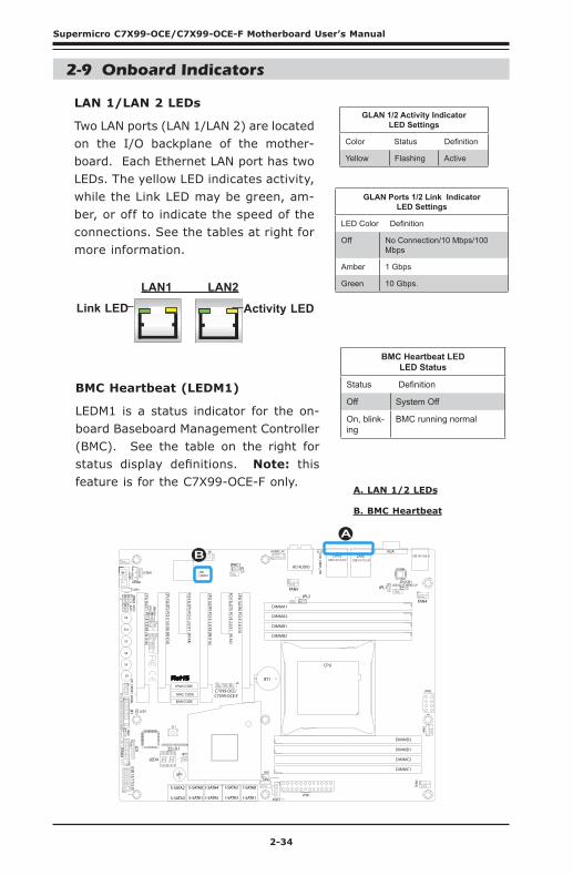
2-34
Supermicro C7X99-OCE/C7X99-OCE-F Motherboard User’s Manual
MAC CODE
IPMI CODE
BAR CODEC7X99-OCE-F
SW_BIOSRC
S4
S7
S10
S5
S6
S9
OC_FRO
NT_PAN
EL
S8
S11
CLR_CMO
S_SW
JUSB30_I2
JAUD
IO1
LED4
I-SATA0I-SATA2I-SATA4S-SATA0S-SATA2
AUDIO_FP
JIPMB1
JSD1
MH11
MH
2
MH9
MH10
JPW2
C A
LEDM1
JBT1
BT1
+
FAN5
FAN4
FAN1
1
FAN2
4FAN3
JPL2
JPUSB1
J29J30
JPME2
JPAC1
JPL1
JI2C1JI2C2
JPB1
JPG1
JWD
11
JL2
JL1
JD1
1JF1
2
19
JPI2C1
JSTBY1
JTPM1
SP1
+
HD AUDIO
VGALAN1LAN2
USB 16/17(3.0)
USB 12/13(3.0) USB 10/11(3.0)USB 14/15(3.0)
CPU SLOT6 PCI-E 3.0 X16
PCH SLOT5 PCI-E 2.0 X1 (IN X4)
CPU SLOT4 PCI-E 3.0 X8 (IN X16)
PCH SLOT3 PCI-E 2.0 X1 (IN X4)
CPU SLOT2 PCI-E 3.0 X8 (IN X16)
CPU SLOT1 PCI-E 3.0 X8 (IN X16)
2-3:DISABLE
1-2:ENABLE
:WATCH
DO
G
SPEAKERPW
R LED
:TPM/PO
RT80
CPU
CHASSIS INTRUSION
JI2C2
2-3:DISABLE
1-2:ENABLE
JI2C1
PWR O
NO
H/FF
NIC1
NIC2
RSTX
CMO
S CLEAR
1-2:NORMAL2-3:BIOS RECOVERY
JBR1
PWR LED
HD
D LED
NM
IX
2-3:ME M
ANU
FACTURIN
G M
OD
E
JPME2
1-2:NO
RMAL
1-2 ENABLE2-3 DISABLE
1-2 ENABLE2-3 DISABLE
:PWR I2C
1-2 ENABLE
2-3 DISABLE
2-3 DISABLE
1-2 ENABLE
1-2 ENABLE2-3 DISABLE
JPAC1
VGA
USB14/15 WAKE UP
1-2 RST2-3 N
MI
:SATA DOM POWER
DIMMD2
DIMMD1
DIMMC2
DIMMC1
DIMMB2
DIMMB1
DIMMA2
DIMMA1
JBR1
JWD
1
JPW1
JPUSB1
JPB1JPG
1
C
A
LED1
I-SATA1I-SATA3I-SATA5S-SATA1S-SATA3
C7X99-OCE/
COM1
A. LAN 1/2 LEDs
B. BMC Heartbeat
A
B
LAN 1/LAN 2 LEDs
Two LAN ports (LAN 1/LAN 2) are located on the I/O backplane of the mother-board. Each Ethernet LAN port has two LEDs. The yellow LED indicates activity, while the Link LED may be green, am-ber, or off to indicate the speed of the connections. See the tables at right for more information.
2-9 Onboard Indicators
LAN1 LAN2
Activity LEDLink LED
BMC Heartbeat LEDLED Status
Status Definition
Off System Off
On, blink-ing
BMC running normal
BMC Heartbeat (LEDM1)
LEDM1 is a status indicator for the on-board Baseboard Management Controller (BMC). See the table on the right for status display definitions. Note: this feature is for the C7X99-OCE-F only.
GLAN Ports 1/2 Link IndicatorLED Settings
LED Color Definition
Off No Connection/10 Mbps/100 Mbps
Amber 1 Gbps
Green 10 Gbps.
GLAN 1/2 Activity IndicatorLED Settings
Color Status Definition
Yellow Flashing Active

Chapter 2: Installation
2-35
Status Display (LED4)
LED4 is made up of two alpha-numeric displays that will display a status or POST code, when the motherboard is powered on. Please download the following AMI publication for a complete list of POST codes:
http://www.ami.com/support/doc/ami_aptio_4.x_status_codes_pub.pdf
MAC CODE
IPMI CODE
BAR CODEC7X99-OCE-F
SW_BIOSRC
S4
S7
S10
S5
S6
S9
OC_FRO
NT_PAN
EL
S8
S11
CLR_CMO
S_SW
JUSB30_I2
JAUD
IO1
LED4
I-SATA0I-SATA2I-SATA4S-SATA0S-SATA2
AUDIO_FP
JIPMB1
JSD1
MH11
MH
2
MH9
MH10
JPW2
C A
LEDM1
JBT1
BT1
+
FAN5
FAN4
FAN1
1
FAN2
4FAN3
JPL2
JPUSB1
J29J30
JPME2
JPAC1
JPL1
JI2C1JI2C2
JPB1
JPG1
JWD
11
JL2
JL1
JD1
1JF1
2
19
JPI2C1
JSTBY1
JTPM1
SP1
+
HD AUDIO
VGALAN1LAN2
USB 16/17(3.0)
USB 12/13(3.0) USB 10/11(3.0)USB 14/15(3.0)
CPU SLOT6 PCI-E 3.0 X16
PCH SLOT5 PCI-E 2.0 X1 (IN X4)
CPU SLOT4 PCI-E 3.0 X8 (IN X16)
PCH SLOT3 PCI-E 2.0 X1 (IN X4)
CPU SLOT2 PCI-E 3.0 X8 (IN X16)
CPU SLOT1 PCI-E 3.0 X8 (IN X16)
2-3:DISABLE
1-2:ENABLE
:WATCH
DO
G
SPEAKERPW
R LED
:TPM/PO
RT80
CPU
CHASSIS INTRUSION
JI2C2
2-3:DISABLE
1-2:ENABLE
JI2C1
PWR O
NO
H/FF
NIC1
NIC2
RSTX
CMO
S CLEAR
1-2:NORMAL2-3:BIOS RECOVERY
JBR1
PWR LED
HD
D LED
NM
IX
2-3:ME M
ANU
FACTURIN
G M
OD
E
JPME2
1-2:NO
RMAL
1-2 ENABLE2-3 DISABLE
1-2 ENABLE2-3 DISABLE
:PWR I2C
1-2 ENABLE
2-3 DISABLE
2-3 DISABLE
1-2 ENABLE
1-2 ENABLE2-3 DISABLE
JPAC1
VGA
USB14/15 WAKE UP
1-2 RST2-3 N
MI
:SATA DOM POWER
DIMMD2
DIMMD1
DIMMC2
DIMMC1
DIMMB2
DIMMB1
DIMMA2
DIMMA1
JBR1
JWD
1
JPW1
JPUSB1
JPB1JPG
1
C
A
LED1
I-SATA1I-SATA3I-SATA5S-SATA1S-SATA3
C7X99-OCE/
COM1
A. Status Display
B. Power LED
A
Note: This feature is for the C7X99-OCE motherboard only.
Power LEDLED Status
Status Definition
Off System Off
On System On and Running
Power LED (LED1)
LED1 is a status LED to indicate that the motherboard is on and running. See the table on the right for status display definitions.
B
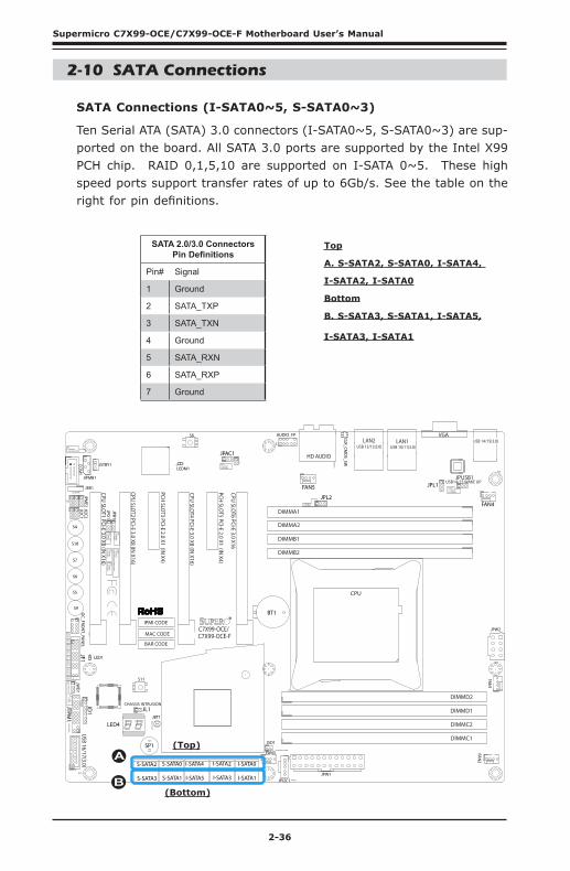
2-36
Supermicro C7X99-OCE/C7X99-OCE-F Motherboard User’s Manual
MAC CODE
IPMI CODE
BAR CODEC7X99-OCE-F
SW_BIOSRC
S4
S7
S10
S5
S6
S9
OC_FRO
NT_PAN
EL
S8
S11
CLR_CMO
S_SW
JUSB30_I2
JAUD
IO1
LED4
I-SATA0I-SATA2I-SATA4S-SATA0S-SATA2
AUDIO_FP
JIPMB1
JSD1
MH11
MH
2
MH9
MH10
JPW2
C A
LEDM1
JBT1
BT1
+
FAN5
FAN4
FAN1
1
FAN2
4FAN3
JPL2
JPUSB1
J29J30
JPME2
JPAC1
JPL1JI2C1JI2C2
JPB1
JPG1
JWD
11
JL2
JL1
JD1
1JF1
2
19
JPI2C1
JSTBY1
JTPM1
SP1
+
HD AUDIO
VGALAN1LAN2
USB 16/17(3.0)
USB 12/13(3.0) USB 10/11(3.0)USB 14/15(3.0)
CPU SLOT6 PCI-E 3.0 X16
PCH SLOT5 PCI-E 2.0 X1 (IN X4)
CPU SLOT4 PCI-E 3.0 X8 (IN X16)
PCH SLOT3 PCI-E 2.0 X1 (IN X4)
CPU SLOT2 PCI-E 3.0 X8 (IN X16)
CPU SLOT1 PCI-E 3.0 X8 (IN X16)
2-3:DISABLE
1-2:ENABLE
:WATCH
DO
G
SPEAKERPW
R LED
:TPM/PO
RT80
CPU
CHASSIS INTRUSION
JI2C2
2-3:DISABLE
1-2:ENABLE
JI2C1
PWR O
NO
H/FF
NIC1
NIC2
RSTX
CMO
S CLEAR
1-2:NORMAL2-3:BIOS RECOVERY
JBR1
PWR LED
HD
D LED
NM
IX
2-3:ME M
ANU
FACTURIN
G M
OD
E
JPME2
1-2:NO
RMAL
1-2 ENABLE2-3 DISABLE
1-2 ENABLE2-3 DISABLE
:PWR I2C
1-2 ENABLE
2-3 DISABLE
2-3 DISABLE
1-2 ENABLE
1-2 ENABLE2-3 DISABLE
JPAC1
VGA
USB14/15 WAKE UP
1-2 RST2-3 N
MI
:SATA DOM POWER
DIMMD2
DIMMD1
DIMMC2
DIMMC1
DIMMB2
DIMMB1
DIMMA2
DIMMA1
JBR1JW
D1
JPW1
JPUSB1
JPB1JPG
1
C
A
LED1
I-SATA1I-SATA3I-SATA5S-SATA1S-SATA3
C7X99-OCE/
COM1
2-10 SATA Connections
SATA Connections (I-SATA0~5, S-SATA0~3)
Ten Serial ATA (SATA) 3.0 connectors (I-SATA0~5, S-SATA0~3) are sup-ported on the board. All SATA 3.0 ports are supported by the Intel X99 PCH chip. RAID 0,1,5,10 are supported on I-SATA 0~5. These high speed ports support transfer rates of up to 6Gb/s. See the table on the right for pin definitions.
SATA 2.0/3.0 Connectors Pin Definitions
Pin# Signal
1 Ground
2 SATA_TXP
3 SATA_TXN
4 Ground
5 SATA_RXN
6 SATA_RXP
7 Ground
Top
A. S-SATA2, S-SATA0, I-SATA4,
I-SATA2, I-SATA0
Bottom
B. S-SATA3, S-SATA1, I-SATA5,
I-SATA3, I-SATA1
A
B
(Top)
(Bottom)

Chapter 2: Installation
2-37
2-10 The OC Front Control Panel (Optional)
The OC (Overclocking) Front Control Panel has Six (6) control buttons, switches and one USB port.
Clean CMOS& Reset
Boot BIOSSwitch
Bios Recovery
BIOS1 BIOS2
OC-1 OC-2 OC-3
Boot BIOS Switch
The Boot BIOS Switch is used to select between two boot BIOS blocks that are installed on the motherboard. See Appendix D for details.
BIOS Recovery
Push the BIOS Recovery button to enable the motherboard to enter the BIOS Recovery process and re-install the BIOS, reverting all settings back to factory default. It looks for a file named "SUPER.ROM" from a memory device attached to any of the USB drives. It functions the same way as the BIOS Restore Button which is installed on the motherboard, see page 2-34.
Front USB Port
The Front USB Port is defined as USB 3.0 Port# XX on this motherboard. It is conveniently located on the OC panel for quick access for USB memory sticks and other storage devices.
Over-Clocking Buttons (OC1, OC2, OC3)
Press these buttons to activate the over-clocking feature of the motherboard. These buttons will allow the CPU to run above its rated speed. This is an advanced feature and should only be used by experienced users. These work the same way as the OC buttons on the motherboard, see Page 2-32 for details.
Clear CMOS and Reset
Use the push-button hardware switch to clear the CMOS memory back to its default values and reset the system. There is also a similar switch on the motherboard (JBT1), but is made up of two contact pads that need to be shorted with a metallic object (i.e., screwdriver, etc).
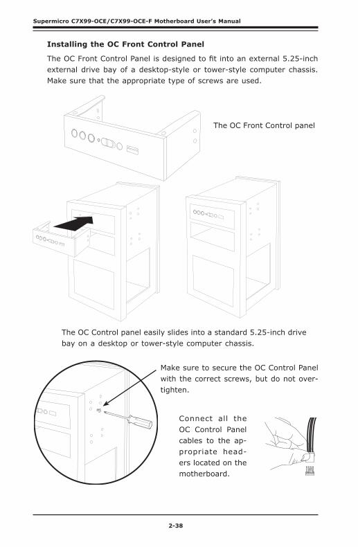
2-38
Supermicro C7X99-OCE/C7X99-OCE-F Motherboard User’s Manual
Installing the OC Front Control Panel
The OC Front Control Panel is designed to fit into an external 5.25-inch external drive bay of a desktop-style or tower-style computer chassis. Make sure that the appropriate type of screws are used.
The OC Front Control panel
The OC Control panel easily slides into a standard 5.25-inch drive bay on a desktop or tower-style computer chassis.
Make sure to secure the OC Control Panel with the correct screws, but do not over-tighten.
Connect all the OC Control Panel cables to the ap-propriate head-ers located on the motherboard.
3-1
Chapter 3: Troubleshooting
Chapter 3
Troubleshooting
3-1 Troubleshooting Procedures
Use the following procedures to troubleshoot your system. If you have followed all of the procedures below and still need assistance, refer to the ‘Technical Support Procedures’ and/or ‘Returning Merchandise for Service’ section(s) in this chapter. Always disconnect the AC power cord before adding, changing or installing any hardware components.
Before Power On
1. Make sure that the Standby PWR LED is not on. (Note: If it is on, the onboard power is on. Be sure to unplug the power cable before installing or removing the components.)
2. Make sure that there are no short circuits between the motherboard and chassis.
3. Disconnect all ribbon/wire cables from the motherboard, including those for the keyboard and mouse. Also, be sure to remove all add-on cards.
4. Install a CPU and heatsink (-be sure that it is fully seated) and then connect the chassis speaker and the power LED to the motherboard. Check all jumper settings as well.
No Power
1. Make sure that there are no short circuits between the motherboard and chassis.
2. Make sure that all jumpers are set to their default positions.
3. Check if the 115V/230V switch on the power supply is properly set.
4. Turn the power switch on and off to test the system.
5. The battery on your motherboard may be old. Check to make sure that it still supplies ~3VDC. If it does not, replace it with a new one.
3-2
Supermicro C7X99-OCE/C7X99-OCE-F Motherboard User’s Manual
No Video
1. If the power is on, but you have no video--in this case, you will need to re-move all the add-on cards and cables first.
2. Use the speaker to determine if any beep codes exist. (Refer to Appendix A for details on beep codes.)
3. Remove all memory modules and turn on the system. (If the alarm is on, check the specifications of memory modules, reset the memory or try a differ-ent one.)
Memory Errors
1. Make sure that the DIMM modules are properly installed and fully seated in the slots.
2. You should be using unbuffered Non-ECC DDR4 memory recommended by the manufacturer. Also, it is recommended that you use the memory modules of the same type and speed for all DIMMs in the system. Do not use memory modules of different sizes, different speeds and different types on the same motherboard.
3. Check for bad DIMM modules or slots by swapping modules between slots to see if you can locate the faulty ones.
4. Check the switch of 115V/230V power supply.
When the System is Losing the Setup Configuration
1. Please be sure to use a high quality power supply. A poor quality power sup-ply may cause the system to lose CMOS setup information. Refer to Section 1-5 for details on recommended power supplies.
2. The battery on your motherboard may be old. Check to verify that it still sup-plies ~3VDC. If it does not, replace it with a new one.
3. If the above steps do not fix the Setup Configuration problem, contact your vendor for repairs.
3-3
Chapter 3: Troubleshooting
3-2 Technical Support Procedures
Before contacting Technical Support, please make sure that you have followed all the steps listed below. Also, Note that as a motherboard manufacturer, Supermicro does not sell directly to end users, so it is best to first check with your distributor or reseller for troubleshooting services. They should know of any possible problem(s) with the specific system configuration that was sold to you.
1. Please go through the ‘Troubleshooting Procedures’ and 'Frequently Asked Question' (FAQ) sections in this chapter or see the FAQs on our website (http://www.supermicro.com/support/faqs/) before contacting Technical Sup-port.
2. BIOS upgrades can be downloaded from our website at (http://www.supermi-cro.com/support/bios/).
Note: Not all BIOS can be flashed. Some cannot be flashed; it depends on the boot block code of the BIOS.
3. If you've followed the instructions above to troubleshoot your system, and still cannot resolve the problem, then contact Supermicro's technical support and provide them with the following information:
• Motherboard model and PCB revision number
• BIOS release date/version (this can be seen on the initial display when your system first boots up)
• System configuration
• An example of a Technical Support form is on our website at (http://www.su-permicro.com/support/contact.cfm).
4. Distributors: For immediate assistance, please have your account number
ready when placing a call to our technical support department. We can be
reached by e-mail at [email protected], by phone at: (408) 503-
8000, option 2, or by fax at (408)503-8019.
3-4
Supermicro C7X99-OCE/C7X99-OCE-F Motherboard User’s Manual
3-3 Frequently Asked Questions
Question: What type of memory does my motherboard support?
Answer: The C7X99-OCE supports up to 64GB of unbuffered Non-ECC/ECC DDR4. See Section 2-4 for details on installing memory.
Question: How do I update my BIOS?
Answer: We do NOT recommend that you upgrade your BIOS if you are not experiencing any problems with your system. Updated BIOS files are located on our website at http://www.supermicro.com/support/bios/. Please check our BIOS warning message and the information on how to update your BIOS on our web site. Select your motherboard model and download the BIOS ROM file to your computer. Also, check the cur-rent BIOS revision to make sure that it is newer than your BIOS before downloading. You may choose the zip file or the .exe file. If you choose the zipped BIOS file, please unzip the BIOS file onto a bootable device or a USB pen/thumb drive. To flash the BIOS, run the batch file named "ami.bat" with the new BIOS ROM file from your bootable device or USB pen/thumb drive. Use the following format:
F:\> ami.bat BIOS-ROM-filename.xxx <Enter>
Note: Always use the file named “ami.bat” to update the BIOS, and insert a space between "ami.bat" and the filename. The BI-OS-ROM-filename will bear the motherboard name (i.e., C7X99) and build version as the extension. For example, "C7X99.115". When completed, your system will automatically reboot.
If you choose the .exe file, please run the .exe file under Win-dows to create the BIOS flash floppy disk. Insert the floppy disk into the system you wish to flash the BIOS. Then, boot the sys-tem to the floppy disk. The BIOS utility will automatically flash the BIOS without any prompts. Please note that this process may take a few minutes to complete. Do not be concerned if the screen is paused for a few minutes.
When the BIOS flashing screen is completed, the system will reboot and will show “Press F1 or F2”. At this point, you will need to load the BIOS defaults. Press <F1> to go to the BIOS setup screen, and press <F9> to load the default settings. Next, press <F10> to save and exit. The system will then reboot.
Attention! Do not shut down or reset the system while updating the BIOS to prevent possible system boot failure!

3-5
Chapter 3: Troubleshooting
3-4 Battery Removal and Installation
Battery Removal
To remove the onboard battery, follow the steps below:
1. Power off your system and unplug your power cable.
2. Locate the onboard battery as shown below.
3. Using a tool such as a pen or a small screwdriver, push the battery lock out-wards to unlock it. Once unlocked, the battery will pop out from the holder.
4. Remove the battery.
Important: The SPI BIOS chip installed on this motherboard is not removable. To repair or replace a damaged BIOS chip, please send your motherboard to RMA at Supermicro for service.
Question: I think my BIOS is corrupted. How can I recover my BIOS?
Answer: Please see Appendix C-BIOS Recovery for detailed instructions.
Battery Lock
Battery
Proper Battery Disposal
Attention! Please handle used batteries carefully. Do not damage the battery in any way; a damaged battery may release hazardous materials into the environment. Do not discard a used battery in the garbage or a public landfill. Please comply with the regulations set up by your local hazardous waste management agency to dispose of your used battery properly.
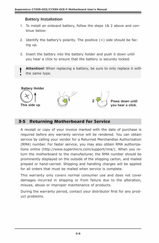
3-6
Supermicro C7X99-OCE/C7X99-OCE-F Motherboard User’s Manual
Battery Holder
1 2
Battery Installation
1. To install an onboard battery, follow the steps 1& 2 above and con-tinue below:
2. Identify the battery's polarity. The positive (+) side should be fac-ing up.
3. Insert the battery into the battery holder and push it down until you hear a click to ensure that the battery is securely locked.
Attention! When replacing a battery, be sure to only replace it with the same type.
This side upPress down until you hear a click.
3-5 Returning Motherboard for Service
A receipt or copy of your invoice marked with the date of purchase is required before any warranty service will be rendered. You can obtain service by calling your vendor for a Returned Merchandise Authorization (RMA) number. For faster service, you may also obtain RMA authoriza-tions online (http://www.supermicro.com/support/rma/). When you re-turn the motherboard to the manufacturer, the RMA number should be prominently displayed on the outside of the shipping carton, and mailed prepaid or hand-carried. Shipping and handling charges will be applied for all orders that must be mailed when service is complete.
This warranty only covers normal consumer use and does not cover damages incurred in shipping or from failure due to the alteration, misuse, abuse or improper maintenance of products.
During the warranty period, contact your distributor first for any prod-uct problems.
Chapter 4: AMI BIOS
4-1
Chapter 4
BIOS
4-1 Introduction
This chapter describes the AMI BIOS Setup Utility for the C7X99-OCE motherboard. The ROM BIOS is stored in a Flash EEPROM and can be easily updated. This chapter describes the basic navigation of the AMI BIOS Setup Utility setup screens.
Note: For AMI BIOS Recovery, please refer to the UEFI BIOS Re-covery Instructions in Appendix C.
Starting BIOS GUI Setup Utility
To enter the AMI BIOS GUI Setup Utility screens, press the <Delete> key while the system is booting up.
Note: In most cases, the <Delete> key is used to invoke the AMI BIOS setup screen.
Each BIOS menu option is described in this manual. The Main BIOS Setup screen has two main areas. The left area is the Main Navigation, and the main area is for the Setup Section. Icons that do not respond when the mouse pointer is hovering on top are not configurable.
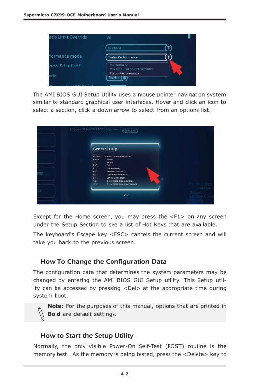
4-2
Supermicro C7X99-OCE Motherboard User’s Manual
Except for the Home screen, you may press the <F1> on any screen under the Setup Section to see a list of Hot Keys that are available.
The keyboard's Escape key <ESC> cancels the current screen and will take you back to the previous screen.
How To Change the Configuration Data
The configuration data that determines the system parameters may be changed by entering the AMI BIOS GUI Setup utility. This Setup util-ity can be accessed by pressing <Del> at the appropriate time during system boot.
Note: For the purposes of this manual, options that are printed in Bold are default settings.
How to Start the Setup Utility
Normally, the only visible Power-On Self-Test (POST) routine is the memory test. As the memory is being tested, press the <Delete> key to
The AMI BIOS GUI Setup Utility uses a mouse pointer navigation system similar to standard graphical user interfaces. Hover and click an icon to select a section, click a down arrow to select from an options list.
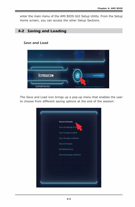
Chapter 4: AMI BIOS
4-3
enter the main menu of the AMI BIOS GUI Setup Utility. From the Setup Home screen, you can access the other Setup Sections.
4-2 Saving and Loading
Save and Load
The Save and Load icon brings up a pop-up menu that enables the user to choose from different saving options at the end of the session:
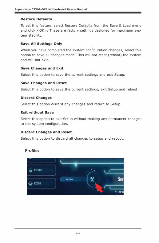
4-4
Supermicro C7X99-OCE Motherboard User’s Manual
Restore Defaults
To set this feature, select Restore Defaults from the Save & Load menu and click <OK>. These are factory settings designed for maximum sys-tem stability.
Save All Settings Only
When you have completed the system configuration changes, select this option to save all changes made. This will not reset (reboot) the system and will not exit.
Save Changes and Exit
Select this option to save the current settings and exit Setup.
Save Changes and Reset
Select this option to save the current settings, exit Setup and reboot.
Discard Changes
Select this option discard any changes and return to Setup.
Exit without Save
Select this option to exit Setup without making any permanent changes to the system configuration.
Discard Changes and Reset
Select this option to discard all changes to setup and reboot.
Profiles
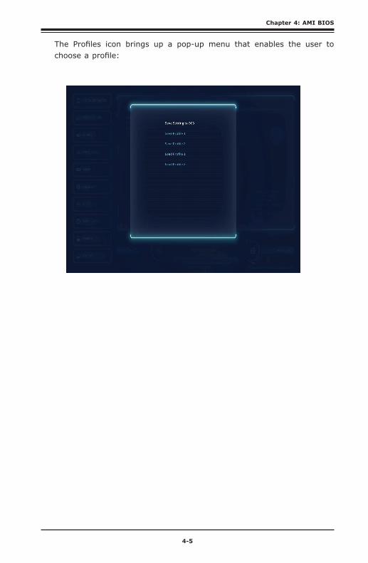
Chapter 4: AMI BIOS
4-5
The Profiles icon brings up a pop-up menu that enables the user to choose a profile:
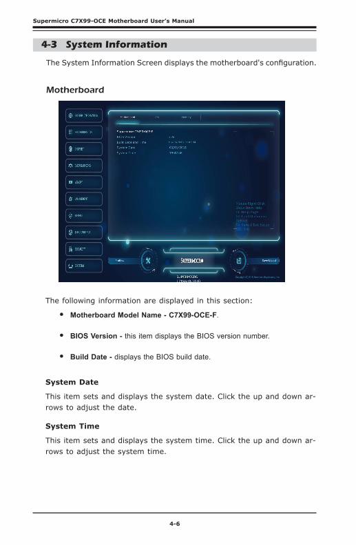
4-6
Supermicro C7X99-OCE Motherboard User’s Manual
4-3 System Information
The System Information Screen displays the motherboard's configuration.
Motherboard
The following information are displayed in this section:
• Motherboard Model Name - C7X99-OCE-F.
• BIOS Version - this item displays the BIOS version number.
• Build Date - displays the BIOS build date.
System Date
This item sets and displays the system date. Click the up and down ar-rows to adjust the date.
System Time
This item sets and displays the system time. Click the up and down ar-rows to adjust the system time.
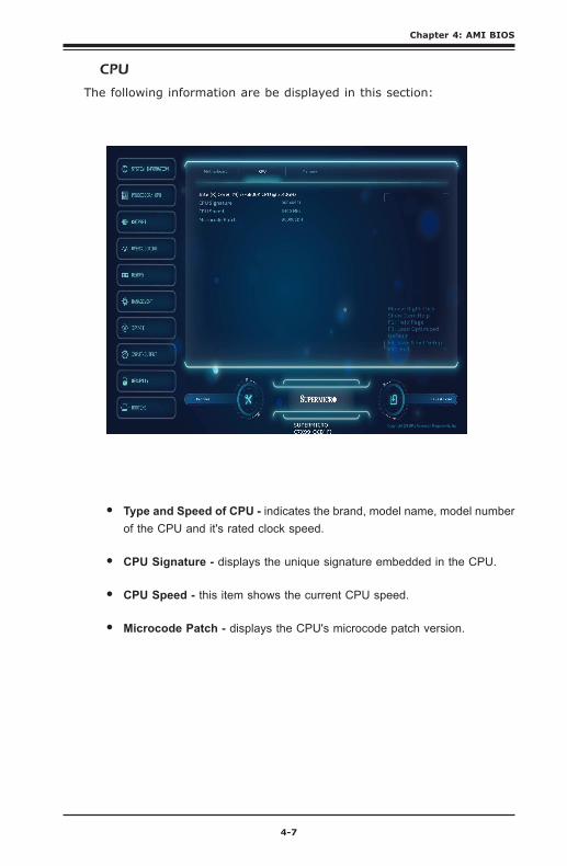
Chapter 4: AMI BIOS
4-7
CPU
The following information are be displayed in this section:
• Type and Speed of CPU - indicates the brand, model name, model number of the CPU and it's rated clock speed.
• CPU Signature - displays the unique signature embedded in the CPU.
• CPU Speed - this item shows the current CPU speed.
• Microcode Patch - displays the CPU's microcode patch version.
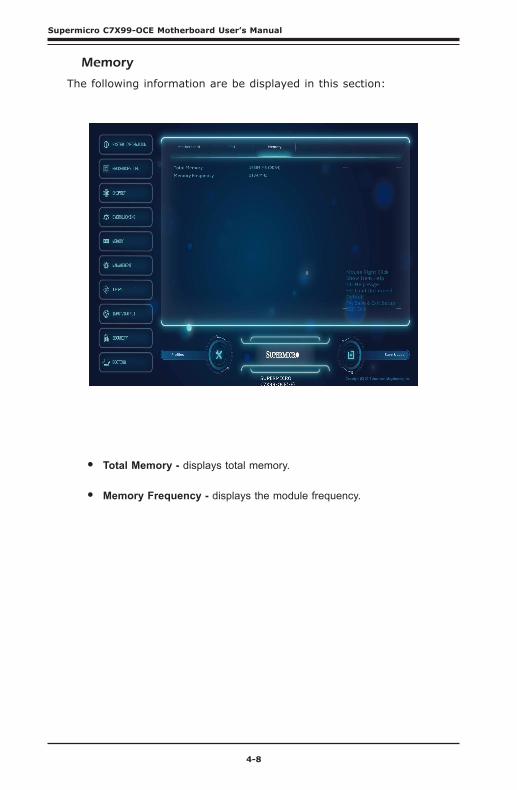
4-8
Supermicro C7X99-OCE Motherboard User’s Manual
Memory
The following information are be displayed in this section:
• Total Memory - displays total memory.
• Memory Frequency - displays the module frequency.
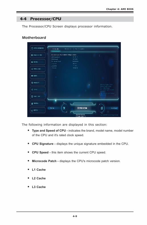
Chapter 4: AMI BIOS
4-9
4-4 Processor/CPU
The Processor/CPU Screen displays processor information.
Motherboard
The following information are displayed in this section:
• Type and Speed of CPU - indicates the brand, model name, model number of the CPU and it's rated clock speed.
• CPU Signature - displays the unique signature embedded in the CPU.
• CPU Speed - this item shows the current CPU speed.
• Microcode Patch - displays the CPU's microcode patch version.
• L1 Cache
• L2 Cache
• L3 Cache
4-10
Supermicro C7X99-OCE Motherboard User’s Manual
Performance
Hyper-Threading [ALL]
Select Enabled to support Intel Hyper-threading Technology to enhance CPU performance. The options are Enabled and Disabled.
Execute Disable Bit (Available if supported by the OS & the CPU)
Select Enabled to enable the Execute-Disable Bit which will allow the processor to designate areas in the system memory where an applica-tion code can execute and where it cannot, thus preventing a worm or a virus from flooding illegal codes to overwhelm the processor or damage the system during an attack. The default is Enabled. (Refer to Intel and Microsoft Web sites for more information.)
Intel® Virtualization Technology
Select Enabled to support Intel Virtualization Technology, which will allow one platform to run multiple operating systems and applications in independent partitions, creating multiple "virtual" systems in one physical computer. The options are Enabled and Disabled.
Note: If a change is made to this setting, you will need to reboot the system for the change to take effect. Refer to Intel’s website for detailed information.
Chapter 4: AMI BIOS
4-11
PPIN Control
Select Enable to unlock the PPIN control. The options are Enabled and Disabled.
Hardware Prefetcher (Available when supported by the CPU)
If set to Enabled, the hardware prefetcher will prefetch streams of data and instructions from the main memory to the L2 cache to improve CPU performance. The options are Disabled and Enabled.
Adjacent Cache Prefetch (Available when supported by the CPU)
The CPU prefetches the cache line for 64 bytes if this feature is set to Disabled. The CPU prefetches both cache lines for 128 bytes as comprised if this feature is set to Enabled.
DCU Streamer Prefetcher (Available when supported by the CPU)
Select Enabled to enable the DCU (Data Cache Unit) Streamer Prefetcher which will stream and prefetch data and send it to the Level 1 data cache to improve data processing and system performance. The options are Disabled and Enabled.
DCU IP Prefetcher (Available when supported by the CPU)
Select Enabled for DCU (Data Cache Unit) IP Prefetcher support, which will prefetch IP addresses to improve network connectivity and system performance. The options are Disabled and Enabled.
Direct Cache Access (DCA Support)
Select Enabled to use Intel's DCA (Direct Cache Access) Technology to improve data transfer efficiency. The options are Enabled and Disabled.
X2APIC
Select Enable to activate APIC (Advanced Programmable Interrupt Con-troller) support. The options are Enabled and Disabled.
AES-NI
Select Enable to use the Intel Advanced Encryption Standard (AES) New Instructions (NI) to ensure data security. The options are Enabled and Disabled.

4-12
Supermicro C7X99-OCE Motherboard User’s Manual
Power Management
Power Technology
Select Energy Efficiency to support power-saving mode. Select Custom to customize system power settings. Select Disabled to disable power-saving settings. The options are Disable, Energy Efficiency, and Custom.
If the above is set to 'Custom' the following options are displayed:
EIST (P-states)
EIST (Enhanced Intel SpeedStep Technology) allows the system to automatically adjust processor voltage and core frequency in an effort to reduce power consumption and heat dissipation. Please refer to Intel’s web site for detailed information. The options are Disabled and Enabled.
Turbo Mode
This feature allows processor cores to run faster than the frequency rec-ommended by the manufacturer. The options are Disabled and Enabled.
Chapter 4: AMI BIOS
4-13
P-state coordination
This feature selects the type of coordination for the P-State of the processor. P-State is a processor operational state that reduces the processor's voltage and frequency. This makes the processor more energy efficient, resulting in further energy gains. The options are HW_ALL, SW_ALL and SW-ANY.
Package C State limit
This feature allows the user to set the limit on the C-State package reg-ister. The options are C0/C1 State, C2 State, C6 (Non Retention) State, and C6 (Rentention) State.
CPU C3 report
Select Enabled to allow the BIOS to report the CPU C3 State (ACPI C2) to the operating system. During the CPU C3 State, the CPU clock generator is turned off. The options are Enabled and Disabled.
CPU C6 report
Select Enabled to allow the BIOS to report the CPU C6 State (ACPI C3) to the operating system. During the CPU C6 State, the power to all cache is turned off. The options are Enabled and Disabled.
Enhanced Halt State (C1E)
Select Enabled to use Enhanced Halt-State technology, which will sig-nificantly reduce the CPU's power consumption by reducing the CPU's clock cycle and voltage during a Halt-state. The options are Disable and Enable.

4-14
Supermicro C7X99-OCE Motherboard User’s Manual
4-5 Chipset
Set all options for the Chipset in this section.
System Agent
The following will be displayed:
• System Agent Bridge Name - this displays the System Agent bridge name.
• System Agent RC Version - indicates the System Agent RC version.
• VT-d Capability - this item indicates whether VT-d is supported.
Enable IOAT
Select Enable to enable Intel I/OAT (I/O Acceleration Technology) sup-port, which significantly reduces CPU overhead by leveraging CPU archi-tectural improvements and freeing the system resource for other tasks. The options are Enable and Disable.
No Snoop
Select Enable to support no-snoop mode for each CB device. The options are Disable and Enable.
Chapter 4: AMI BIOS
4-15
Relaxed Ordering
Select Enable to enable Relaxed Ordering support which will allow certain transactions to violate the strict-ordering rules of PCI bus for a transac-tion to be completed prior to other transactions that have already been enqueued. The options are Disable and Enable.
Intel VT for Directed I/O (VT-d)
Select Enabled to enable Intel Virtualization Technology support for Direct I/O VT-d by reporting the I/O device assignments to the Virtual Machine Manager (VMM) through the DMAR ACPI Tables. This feature offers fully-protected I/O resource-sharing across the Intel platforms, providing the user with greater reliability, security and availability in networking and data-sharing. The settings are Enabled and Disabled.
Interrupt Remapping
Select Enable for Interrupt Remapping support to enhance system per-formance. The options are Enable and Disable.
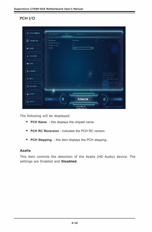
4-16
Supermicro C7X99-OCE Motherboard User’s Manual
PCH I/O
The following will be displayed:
• PCH Name - this displays the chipset name.
• PCH RC Reversion - indicates the PCH RC version.
• PCH Stepping - this item displays the PCH stepping..
Azalia
This item controls the detection of the Azalia (HD Audio) device. The settings are Enabled and Disabled.
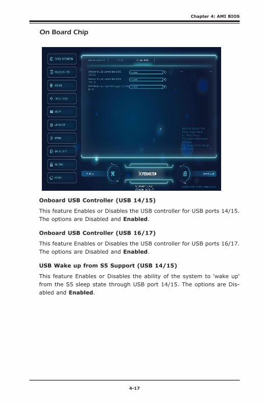
Chapter 4: AMI BIOS
4-17
On Board Chip
Onboard USB Controller (USB 14/15)
This feature Enables or Disables the USB controller for USB ports 14/15. The options are Disabled and Enabled.
Onboard USB Controller (USB 16/17)
This feature Enables or Disables the USB controller for USB ports 16/17. The options are Disabled and Enabled.
USB Wake up from S5 Support (USB 14/15)
This feature Enables or Disables the ability of the system to 'wake up' from the S5 sleep state through USB port 14/15. The options are Dis-abled and Enabled.
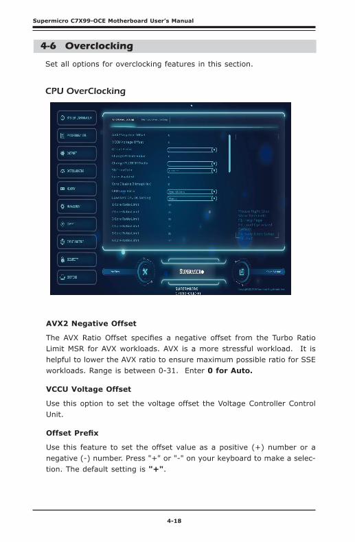
4-18
Supermicro C7X99-OCE Motherboard User’s Manual
AVX2 Negative Offset
The AVX Ratio Offset specifies a negative offset from the Turbo Ratio Limit MSR for AVX workloads. AVX is a more stressful workload. It is helpful to lower the AVX ratio to ensure maximum possible ratio for SSE workloads. Range is between 0-31. Enter 0 for Auto.
VCCU Voltage Offset
Use this option to set the voltage offset the Voltage Controller Control Unit.
Offset Prefix
Use this feature to set the offset value as a positive (+) number or a negative (-) number. Press "+" or "-" on your keyboard to make a selec-tion. The default setting is "+".
4-6 Overclocking
Set all options for overclocking features in this section.
CPU OverClocking
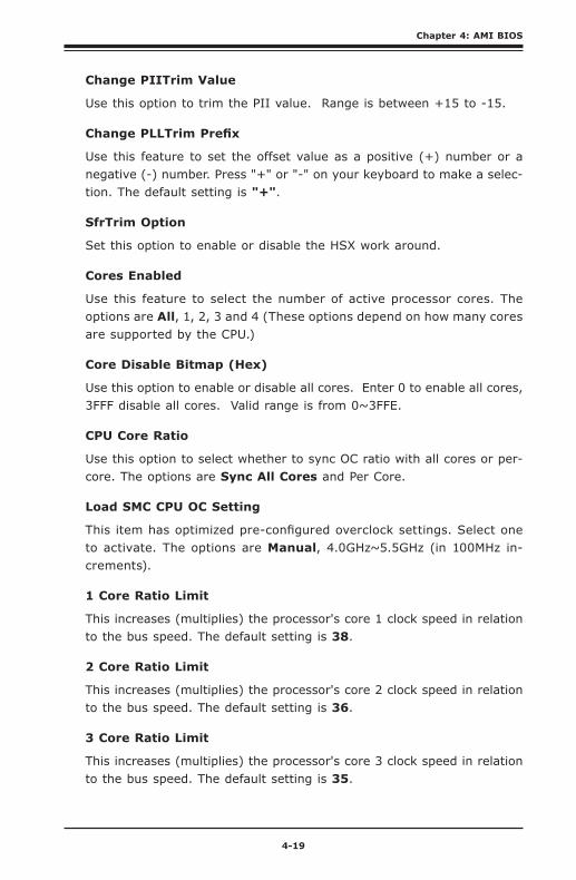
Chapter 4: AMI BIOS
4-19
Change PIITrim Value
Use this option to trim the PII value. Range is between +15 to -15.
Change PLLTrim Prefix
Use this feature to set the offset value as a positive (+) number or a negative (-) number. Press "+" or "-" on your keyboard to make a selec-tion. The default setting is "+".
SfrTrim Option
Set this option to enable or disable the HSX work around.
Cores Enabled
Use this feature to select the number of active processor cores. The options are All, 1, 2, 3 and 4 (These options depend on how many cores are supported by the CPU.)
Core Disable Bitmap (Hex)
Use this option to enable or disable all cores. Enter 0 to enable all cores, 3FFF disable all cores. Valid range is from 0~3FFE.
CPU Core Ratio
Use this option to select whether to sync OC ratio with all cores or per-core. The options are Sync All Cores and Per Core.
Load SMC CPU OC Setting
This item has optimized pre-configured overclock settings. Select one to activate. The options are Manual, 4.0GHz~5.5GHz (in 100MHz in-crements).
1 Core Ratio Limit
This increases (multiplies) the processor's core 1 clock speed in relation to the bus speed. The default setting is 38.
2 Core Ratio Limit
This increases (multiplies) the processor's core 2 clock speed in relation to the bus speed. The default setting is 36.
3 Core Ratio Limit
This increases (multiplies) the processor's core 3 clock speed in relation to the bus speed. The default setting is 35.
4-20
Supermicro C7X99-OCE Motherboard User’s Manual
4 Core Ratio Limit
This increases (multiplies) the processor's core 4 clock speed in relation to the bus speed. The default setting is 35.
5 Core Ratio Limit
This increases (multiplies) the processor's core 5 clock speed in relation to the bus speed. The default setting is 35.
6 Core Ratio Limit
This increases (multiplies) the processor's core 6 clock speed in relation to the bus speed. The default setting is 35.
CPU Cache Ratio
Set this option to configure the CPU Internal Bus Speed Ratio. The maxi-mum should be the same as the CPU Ratio.
BCLK Ratio
This option is used to set the Base Clock (BCLK) ratio. The options are 1.00, 1.25, 1.67, 2.50
BCLK Clock Frequency (1/100 MHz)
Use this item to set the CPU clock override value for the host system. The default setting is 10000.
LCPLL or SBPLL select
If PEG/DMI Ratio (above) is set to other than 1.00, this option can be configured to select between LCPLL ("LC" is a type of Inductor/Capaci-tor resonator) or SBPLL (Self-Biased Phase Lock Loop). The options are SBPLL, and LCPLL.
CPU Non Turbo Ratio Override
Use this item to set CPU ratio override when not in turbo mode. The default setting is dependent on the type of CPU installed.
CPU Power Setting
Enhanced Intel SpeedStep Technology
Intel SpeedStep Technology allows the system to automatically adjust processor voltage and core frequency to reduce power consumption and heat dissipation. The options are Disabled and Enabled.
Chapter 4: AMI BIOS
4-21
Turbo Mode
This feature allows processor cores to run faster than the frequency rec-ommended by the manufacturer. The options are Disabled and Enabled.
CPU Non-Turbo Setting
Package TDP Lock Enable
Select Enabled to lock the Thermal Design Power (TDP) value for the processor. The options are Disabled and Enabled.
Long Duration Power Limit (Watt)
This feature configures Package Power Limit 1, in watts. When the limit is exceeded, the CPU ratio is lowered after a period of time (see item below). A lower limit can save power and protect the CPU, while a higher limit improves performance. Use the number keys on your keyboard to enter the value. The default setting is dependent on the CPU.
Long Duration Power Limit Time (Seconds)
This item allows the user to determine how long the CPU should operate at the power limit set by the user for the item above, if the power limit is exceeded. Use the number keys on your keyboard to enter the value. The default setting is 8.
Short Duration Power Limit Switch
Select Enabled for power limit switch Package Power Limit 2. The settings are Disabled and Enabled.
Short Duration Power Limit (Watt)
This feature configures Package Power Limit 2, in watts. When the limit is exceeded, the CPU ratio is lowered immediately. A lower limit can save power and protect the CPU, while a higher limit improves performance. Use the number keys on your keyboard to enter the value. The default setting is dependent on the CPU. The default setting is dependent on the CPU.
Package Current Lock
Select Enabled to lock the current CPU package values. The options are Enabled and Disabled.
Processor Current Limit (1/8 Amp)
This feature allows the user to set the maximum electric current value for the Intel CPU cores. The default setting is dependent on the type of CPU installed.
4-22
Supermicro C7X99-OCE Motherboard User’s Manual
Disable OverClocking Lock
If this feature is set to Enabled, the OverClocking Lock will be deactivated. The options are Disabled and Enabled.
Voltage Configuration
CPU Voltage Mode
Use this feature to select the CPU voltage mode. The options are Over-ride and Adaptive.
CPU Adaptive Voltage Target (mV)
Use this feature to set the CPU voltage Target(mV) value from 0mV to 2000mV. Enter 0 to use the manufacture default value.
CPU Voltage Offset (mV)
Use this feature to set the CPU Voltage Offset value from -1000mV to 998mV. Enter 0 to use the manufacture default value.
Offset Prefix
Use this feature to set the offset value as a positive (+) number or a negative (-) number. The default setting is "+".
Overclocking SVID and FIVR Option
Load Line Calibration
Enabling this feature adjusts Vdroop, keeping the CPU voltage more con-stant under light and heavy CPU load The options are Level 0 ~ Level 9.
CPU Input Voltage
Use this feature to set the CPU input voltage. The options are 1.81V, 1.85V, 1.90V, 1.95V, 2.00V, 2.05V, 2.10V, 2.15V, 2.20V and 2.25V.
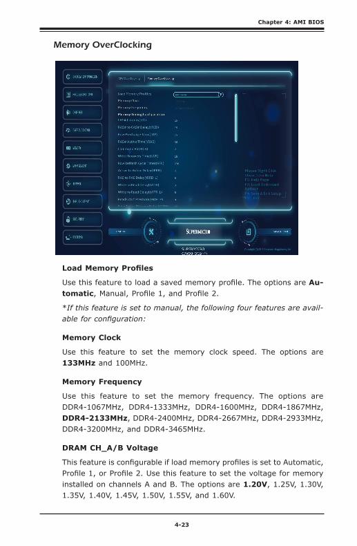
Chapter 4: AMI BIOS
4-23
Memory OverClocking
Load Memory Profiles
Use this feature to load a saved memory profile. The options are Au-tomatic, Manual, Profile 1, and Profile 2.
*If this feature is set to manual, the following four features are avail-able for configuration:
Memory Clock
Use this feature to set the memory clock speed. The options are 133MHz and 100MHz.
Memory Frequency
Use this feature to set the memory frequency. The options are DDR4-1067MHz, DDR4-1333MHz, DDR4-1600MHz, DDR4-1867MHz, DDR4-2133MHz, DDR4-2400MHz, DDR4-2667MHz, DDR4-2933MHz, DDR4-3200MHz, and DDR4-3465MHz.
DRAM CH_A/B Voltage
This feature is configurable if load memory profiles is set to Automatic, Profile 1, or Profile 2. Use this feature to set the voltage for memory installed on channels A and B. The options are 1.20V, 1.25V, 1.30V, 1.35V, 1.40V, 1.45V, 1.50V, 1.55V, and 1.60V.
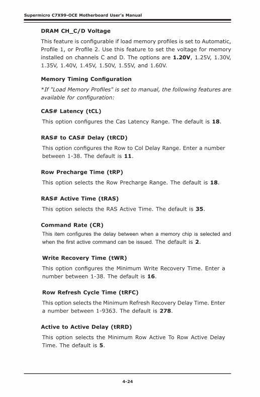
4-24
Supermicro C7X99-OCE Motherboard User’s Manual
DRAM CH_C/D Voltage
This feature is configurable if load memory profiles is set to Automatic, Profile 1, or Profile 2. Use this feature to set the voltage for memory installed on channels C and D. The options are 1.20V, 1.25V, 1.30V, 1.35V, 1.40V, 1.45V, 1.50V, 1.55V, and 1.60V.
Memory Timing Configuration
*If "Load Memory Profiles" is set to manual, the following features are available for configuration:
CAS# Latency (tCL)
This option configures the Cas Latency Range. The default is 18.
RAS# to CAS# Delay (tRCD)
This option configures the Row to Col Delay Range. Enter a number between 1-38. The default is 11.
Row Precharge Time (tRP)
This option selects the Row Precharge Range. The default is 18.
RAS# Active Time (tRAS)
This option selects the RAS Active Time. The default is 35.
Command Rate (CR)This item configures the delay between when a memory chip is selected and when the first active command can be issued. The default is 2.
Write Recovery Time (tWR)
This option configures the Minimum Write Recovery Time. Enter a number between 1-38. The default is 16.
Row Refresh Cycle Time (tRFC)
This option selects the Minimum Refresh Recovery Delay Time. Enter a number between 1-9363. The default is 278.
Active to Active Delay (tRRD)
This option selects the Minimum Row Active To Row Active Delay Time. The default is 5.
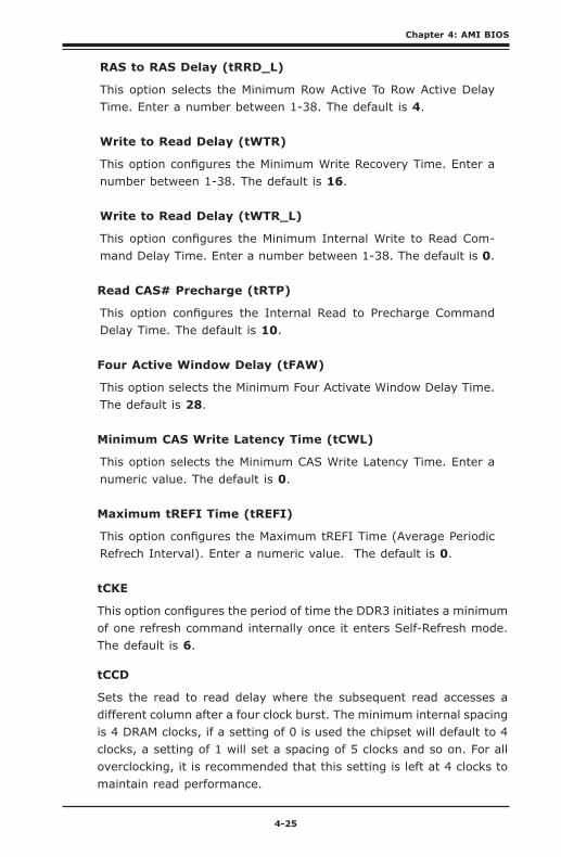
Chapter 4: AMI BIOS
4-25
RAS to RAS Delay (tRRD_L)
This option selects the Minimum Row Active To Row Active Delay Time. Enter a number between 1-38. The default is 4.
Write to Read Delay (tWTR)
This option configures the Minimum Write Recovery Time. Enter a number between 1-38. The default is 16.
Write to Read Delay (tWTR_L)
This option configures the Minimum Internal Write to Read Com-mand Delay Time. Enter a number between 1-38. The default is 0.
Read CAS# Precharge (tRTP)
This option configures the Internal Read to Precharge Command Delay Time. The default is 10.
Four Active Window Delay (tFAW)
This option selects the Minimum Four Activate Window Delay Time. The default is 28.
Minimum CAS Write Latency Time (tCWL)
This option selects the Minimum CAS Write Latency Time. Enter a numeric value. The default is 0.
Maximum tREFI Time (tREFI)
This option configures the Maximum tREFI Time (Average Periodic Refrech Interval). Enter a numeric value. The default is 0.
tCKE
This option configures the period of time the DDR3 initiates a minimum of one refresh command internally once it enters Self-Refresh mode. The default is 6.
tCCD
Sets the read to read delay where the subsequent read accesses a different column after a four clock burst. The minimum internal spacing is 4 DRAM clocks, if a setting of 0 is used the chipset will default to 4 clocks, a setting of 1 will set a spacing of 5 clocks and so on. For all overclocking, it is recommended that this setting is left at 4 clocks to maintain read performance.
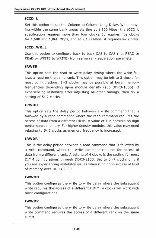
4-26
Supermicro C7X99-OCE Motherboard User’s Manual
tCCD_L
Set this option to set the Column to Column Long Delay. When stay-ing within the same bank group starting at 1,600 Mbps, the tCCD_L specification requires more than four clocks. It requires five clocks for 1,600 and 1,866 Mbps, and at 2,133 Mbps, it requires six clocks.
tCCD_WR_L
Use this option to configure back to back CAS to CAS (i.e. READ to REaD or WRITE to WRITE) from same rank separation parameter.
tRWSR
This option sets the read to write delay timing where the write fol-lows a read on the same rank. This option may be left to 3 clocks for most configurations. 1~2 clocks may be possible at lower memory frequencies depending upon module density (sub DDR3-1866). If experiencing instability after adjusting all other timings, then try a setting of 5~7 clocks.
tRWDD
This option sets the delay period between a write command that is followed by a read command; where the read command requires the access of data from a different DIMM. A value of 1 is possible on high performance memory. For higher density modules this value may need relaxing to 5~6 clocks as memory frequency is increased.
tRWDR
This is the delay period between a read command that is followed by a write command, where the write command requires the access of data from a different rank. A setting of 4 clocks is the setting for most DIMM configurations through DDR3-2133. Set to 5~7 clocks only if you are experiencing instability issues when running in excess of 8GB of memory over DDR3-2300.
tWWDD
This option configures the write to write delay where the subsequent write requires the access of a different DIMM. 4 clocks will work with most configurations.
tWWDR
This option configures the write to write delay where the subsequent write command requires the access of a different rank on the same DIMM.
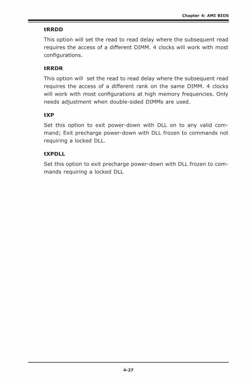
Chapter 4: AMI BIOS
4-27
tRRDD
This option will set the read to read delay where the subsequent read requires the access of a different DIMM. 4 clocks will work with most configurations.
tRRDR
This option will set the read to read delay where the subsequent read requires the access of a different rank on the same DIMM. 4 clocks will work with most configurations at high memory frequencies. Only needs adjustment when double-sided DIMMs are used.
tXP
Set this option to exit power-down with DLL on to any valid com-mand; Exit precharge power-down with DLL frozen to commands not requiring a locked DLL.
tXPDLL
Set this option to exit precharge power-down with DLL frozen to com-mands requiring a locked DLL
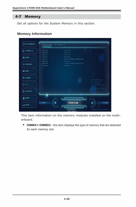
4-28
Supermicro C7X99-OCE Motherboard User’s Manual
This item information on the memory modules installed on the moth-erboard.
• DIMMA1~DIMMD2 - this item displays the type of memory that are detected for each memory slot.
4-7 Memory
Set all options for the System Memory in this section.
Memory Information
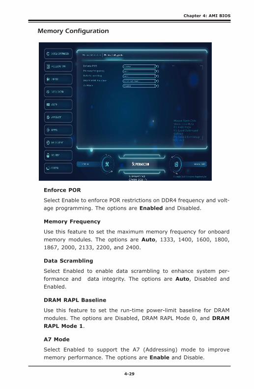
Chapter 4: AMI BIOS
4-29
Memory Configuration
Enforce POR
Select Enable to enforce POR restrictions on DDR4 frequency and volt-age programming. The options are Enabled and Disabled.
Memory Frequency
Use this feature to set the maximum memory frequency for onboard memory modules. The options are Auto, 1333, 1400, 1600, 1800, 1867, 2000, 2133, 2200, and 2400.
Data Scrambling
Select Enabled to enable data scrambling to enhance system per-formance and data integrity. The options are Auto, Disabled and Enabled.
DRAM RAPL Baseline
Use this feature to set the run-time power-limit baseline for DRAM modules. The options are Disabled, DRAM RAPL Mode 0, and DRAM RAPL Mode 1.
A7 Mode
Select Enabled to support the A7 (Addressing) mode to improve memory performance. The options are Enable and Disable.
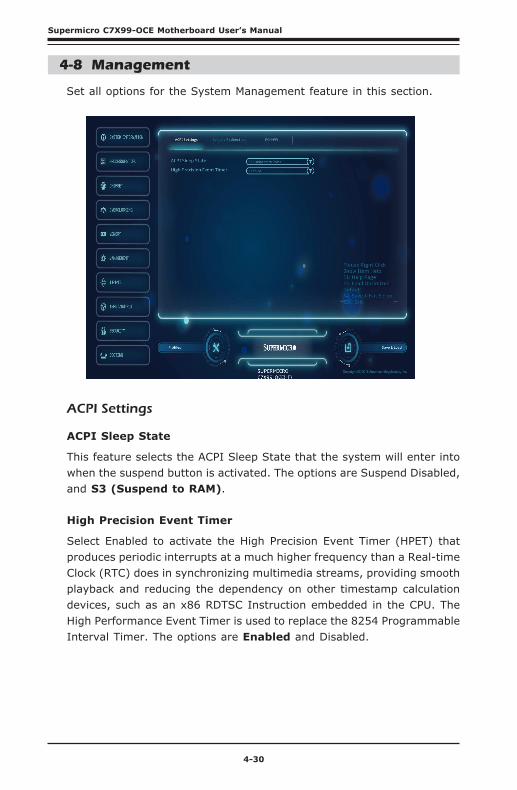
4-30
Supermicro C7X99-OCE Motherboard User’s Manual
ACPI Settings
ACPI Sleep State
This feature selects the ACPI Sleep State that the system will enter into when the suspend button is activated. The options are Suspend Disabled, and S3 (Suspend to RAM).
High Precision Event Timer
Select Enabled to activate the High Precision Event Timer (HPET) that produces periodic interrupts at a much higher frequency than a Real-time Clock (RTC) does in synchronizing multimedia streams, providing smooth playback and reducing the dependency on other timestamp calculation devices, such as an x86 RDTSC Instruction embedded in the CPU. The High Performance Event Timer is used to replace the 8254 Programmable Interval Timer. The options are Enabled and Disabled.
4-8 Management
Set all options for the System Management feature in this section.
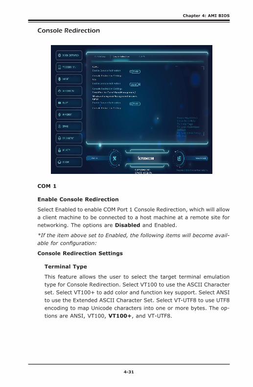
Chapter 4: AMI BIOS
4-31
COM 1
Enable Console Redirection
Select Enabled to enable COM Port 1 Console Redirection, which will allow a client machine to be connected to a host machine at a remote site for networking. The options are Disabled and Enabled.
*If the item above set to Enabled, the following items will become avail-able for configuration:
Console Redirection Settings
Terminal Type
This feature allows the user to select the target terminal emulation type for Console Redirection. Select VT100 to use the ASCII Character set. Select VT100+ to add color and function key support. Select ANSI to use the Extended ASCII Character Set. Select VT-UTF8 to use UTF8 encoding to map Unicode characters into one or more bytes. The op-tions are ANSI, VT100, VT100+, and VT-UTF8.
Console Redirection

4-32
Supermicro C7X99-OCE Motherboard User’s Manual
Bits Per second
Use this item to set the transmission speed for a serial port used in Console Redirection. Make sure that the same speed is used in the host computer and the client computer. A lower transmission speed may be required for long and busy lines. The options are 9600, 19200, 38400, 57600 and 115200 (bits per second).
Data Bits
Use this feature to set the data transmission size for Console Redirec-tion. The options are 7 (Bits) and 8 (Bits).
Parity
A parity bit can be sent along with regular data bits to detect data transmission errors. Select Even if the parity bit is set to 0, and the number of 1's in data bits is even. Select Odd if the parity bit is set to 0, and the number of 1's in data bits is odd. Select None if you do not want to send a parity bit with your data bits in transmission. Select Mark to add a mark as a parity bit to be sent along with the data bits. Select Space to add a Space as a parity bit to be sent with your data bits. The options are None, Even, Odd, Mark and Space.
Stop Bits
A stop bit indicates the end of a serial data packet. Select 1 Stop Bit for standard serial data communication. Select 2 Stop Bits if slower devices are used. The options are 1 and 2.
Flow Control
Use this item to set the flow control for Console Redirection to pre-vent data loss caused by buffer overflow. Send a "Stop" signal to stop sending data when the receiving buffer is full. Send a "Start" signal to start sending data when the receiving buffer is empty. The options are None and Hardware RTS/CTS.
VT-UTF8 Combo Key Support
Select Enabled to enable VT-UTF8 Combination Key support for ANSI/VT100 terminals. The options are Enabled and Disabled.
Recorder Mode
Select Enabled to capture the data displayed on a terminal and send it as text messages to a remote server. The options are Enabled and Disabled.
Chapter 4: AMI BIOS
4-33
Resolution 100x31
Select Enabled for extended-terminal resolution support. The options are Enabled and Disabled.
Legacy OS Redirection Resolution
Use this item to select the number of rows and columns used in Console Redirection for legacy OS support. The options are 80x24 and 80x25.
Putty KeyPad
This feature selects Function Keys and KeyPad settings for Putty, which is a terminal emulator designed for the Windows OS. The options are VT100, LINUX, XTERMR6, SCO, ESCN, and VT400.
Redirection After BIOS Post
Use this feature to enable or disable legacy Console Redirection after BIOS POST. When the option-Bootloader is selected, legacy Console Redirection is disabled before booting the OS. When the option- Always Enable is selected, legacy Console Redirection remains enabled upon OS bootup. The options are Always Enable and Bootloader.
SOL
Enable Console Redirection
Select Enabled to use the SOL port for Console Redirection. The options are Enabled and Disabled.
*If the item above is set to Enabled, the following items will become available for user's configuration:
Console Redirection Settings
Terminal Type
Use this feature to select the target terminal emulation type for Con-sole Redirection. Select VT100 to use the ASCII Character set. Select VT100+ to add color and function key support. Select ANSI to use the Extended ASCII Character Set. Select VT-UTF8 to use UTF8 encoding to map Unicode characters into one or more bytes. The options are ANSI, VT100, VT100+, and VT-UTF8.
4-34
Supermicro C7X99-OCE Motherboard User’s Manual
Bits Per second
Use this feature to set the transmission speed for a serial port used in Console Redirection. Make sure that the same speed is used in the host computer and the client computer. A lower transmission speed may be required for long and busy lines. The options are 9600, 19200, 38400, 57600 and 115200 (bits per second).
Data Bits
Use this feature to set the data transmission size for Console Redirec-tion. The options are 7 (Bits) and 8 (Bits).
Parity
A parity bit can be sent along with regular data bits to detect data transmission errors. Select Even if the parity bit is set to 0, and the number of 1's in data bits is even. Select Odd if the parity bit is set to 0, and the number of 1's in data bits is odd. Select None if you do not want to send a parity bit with your data bits in transmission. Select Mark to add a mark as a parity bit to be sent along with the data bits. Select Space to add a Space as a parity bit to be sent with your data bits. The options are None, Even, Odd, Mark and Space.
Stop Bits
A stop bit indicates the end of a serial data packet. Select 1 Stop Bit for standard serial data communication. Select 2 Stop Bits if slower devices are used. The options are 1 and 2.
Flow Control
Use this feature to set the flow control for Console Redirection to pre-vent data loss caused by buffer overflow. Send a "Stop" signal to stop sending data when the receiving buffer is full. Send a "Start" signal to start data-sending when the receiving buffer is empty. The options are None and Hardware RTS/CTS.
VT-UTF8 Combo Key Support
Select Enabled to enable VT-UTF8 Combination Key support for ANSI/VT100 terminals. The options are Enabled and Disabled.
Recorder Mode
Select Enabled to capture the data displayed on a terminal and send it as text messages to a remote server. The options are Disabled and Enabled.
Chapter 4: AMI BIOS
4-35
Resolution 100x31
Select Enabled for extended-terminal resolution support. The options are Disabled and Enabled.
Legacy OS Redirection Resolution
Use this feature to select the number of rows and columns used in Console Redirection for legacy OS support. The options are 80x24 and 80x25.
Putty KeyPad
This feature selects Function Keys and KeyPad settings for Putty, which is a terminal emulator designed for the Windows OS. The options are VT100, LINUX, XTERMR6, SCO, ESCN, and VT400.
Redirection After BIOS Post
Use this feature to enable or disable legacy Console Redirection after BIOS POST (Power-On Self-Test). When this feature is set to Boot-loader, legacy Console Redirection is disabled before booting the OS. When this feature is set to Always Enable, legacy Console Redirection remains enabled upon OS boot. The options are Always Enable and Bootloader.
Serial Port for Out-of-Band Management/Windows Emergency Management Services (EMS)
The submenu allows the user to configure Console Redirection settings to support Out-of-Band Serial Port management.
Enable Console Redirection
Select Enabled to use a COM port selected by the user for EMS Console Redirection. The options are Enabled and Disabled.
*If the item above set to Enabled, the following items will become avail-able for user's configuration:
Console Redirection Settings
Out-of-Band Management Port
The feature selects a serial port in a client server to be used by the Windows Emergency Management Services (EMS) to communicate with a remote host server. The options are COM1 and SOL.
4-36
Supermicro C7X99-OCE Motherboard User’s Manual
Terminal Type
Use this feature to select the target terminal emulation type for Con-sole Redirection. Select VT100 to use the ASCII character set. Select VT100+ to add color and function key support. Select ANSI to use the extended ASCII character set. Select VT-UTF8 to use UTF8 encoding to map Unicode characters into one or more bytes. The options are ANSI, VT100, VT100+, and VT-UTF8.
Bits Per Second
This item sets the transmission speed for a serial port used in Con-sole Redirection. Make sure that the same speed is used in both host computer and the client computer. A lower transmission speed may be required for long and busy lines. The options are 9600, 19200, 57600, and 115200 (bits per second).
Flow Control
Use this item to set the flow control for Console Redirection to pre-vent data loss caused by buffer overflow. Send a "Stop" signal to stop data-sending when the receiving buffer is full. Send a "Start" signal to start data-sending when the receiving buffer is empty. The options are None, Hardware RTS/CTS, and Software Xon/Xoff.
The setting for each of these features is displayed:
Data Bits, Parity, Stop Bits
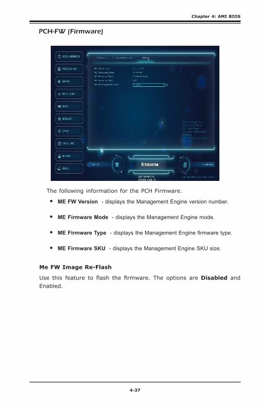
Chapter 4: AMI BIOS
4-37
PCH-FW (Firmware)
The following information for the PCH Firmware.
• ME FW Version - displays the Management Engine version number.
• ME Firmware Mode - displays the Management Engine mode.
• ME Firmware Type - displays the Management Engine firmware type.
• ME Firmware SKU - displays the Management Engine SKU size.
Me FW Image Re-Flash
Use this feature to flash the firmware. The options are Disabled and Enabled.
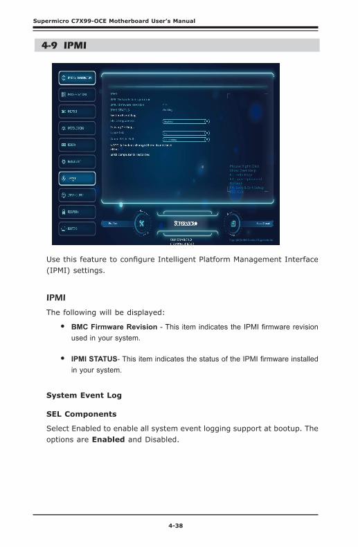
4-38
Supermicro C7X99-OCE Motherboard User’s Manual
4-9 IPMI
Use this feature to configure Intelligent Platform Management Interface (IPMI) settings.
IPMI
The following will be displayed:
• BMC Firmware Revision - This item indicates the IPMI firmware revision used in your system.
• IPMI STATUS- This item indicates the status of the IPMI firmware installed in your system.
System Event Log
SEL Components
Select Enabled to enable all system event logging support at bootup. The options are Enabled and Disabled.
Chapter 4: AMI BIOS
4-39
Erasing Settings
Erase SEL
Select Yes, On next reset to erase all system event logs upon next sys-tem reboot. Select Yes, On every reset to erase all system event logs upon each system reboot. Select No to keep all system event logs after each system reboot. The options are No, Yes, On next reset, and Yes, On every reset.
When SEL is Full
This feature allows the user to determine what the BIOS should do when the system event log is full. Select Erase Immediately to erase all events in the log when the system event log is full. The options are Do Nothing and Erase Immediately.
Note: After making changes on a setting, be sure to reboot the system for the changes to take effect.
BMC Network Configuration
The following items will be displayed:
BMC Network Configuration
• IPMI LAN Selection - IPMI LAN Selection status
• IPMI Network Link Status - Connection status
Update IPMI LAN Configuration
Select Yes for the system BIOS to automatically reset the following IPMI settings at next system boot. The options are Yes and No.
Configuration Address Source (Available when the item above - Update IPMI LAN Configuration is set to Yes)
Use this item to select the IP address source for this computer. If Static is selected, you will need to know the IP address of this computer and enter it to the system manually in the field. If DHCP is selected, AMI BIOS will search for a DHCP (Dynamic Host Configuration Protocol) server attached to the network and request the next available IP address for this computer. The options are DHCP and Static.
4-40
Supermicro C7X99-OCE Motherboard User’s Manual
Station MAC Address
This item displays the Station MAC address for this computer. Mac ad-dresses are 6 two-digit hexadecimal numbers.
Station IP Address
This item displays the Station IP address for this computer. This should be in decimal and in dotted quad form (i.e., 192.168.10.253).
Subnet Mask
This item displays the sub-network that this computer belongs to. The value of each three-digit number is separated by dots and it should not exceed 255.
Gateway IP Address
This item displays the Gateway IP address for this computer. This should be in decimal and in dotted quad form (i.e., 192.168.10.253).
When you have completed the system configuration changes, select this option to save the changes and reboot the computer so that the new system configuration settings can take effect. Select Save Changes and Exit, and press <Enter>. When the dialog box appears, asking you if you want to exit the BIOS setup without saving, click Yes to quit BIOS with-out saving the changes, or click No to quit the BIOS and save changes.
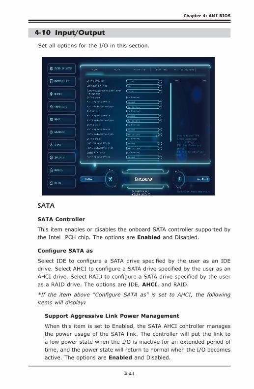
Chapter 4: AMI BIOS
4-41
4-10 Input/Output
Set all options for the I/O in this section.
SATA
SATA Controller
This item enables or disables the onboard SATA controller supported by the Intel PCH chip. The options are Enabled and Disabled.
Configure SATA as
Select IDE to configure a SATA drive specified by the user as an IDE drive. Select AHCI to configure a SATA drive specified by the user as an AHCI drive. Select RAID to configure a SATA drive specified by the user as a RAID drive. The options are IDE, AHCI, and RAID.
*If the item above "Configure SATA as" is set to AHCI, the following items will display:
Support Aggressive Link Power Management
When this item is set to Enabled, the SATA AHCI controller manages the power usage of the SATA link. The controller will put the link to a low power state when the I/O is inactive for an extended period of time, and the power state will return to normal when the I/O becomes active. The options are Enabled and Disabled.
4-42
Supermicro C7X99-OCE Motherboard User’s Manual
SATA Port 0 ~ SATA Port 5
This item displays the information detected on the installed SATA drive on the particular SATA port.
• Model number of drive and capacity
Port 0 ~ Port 5 Spin Up Device
On an edge detect from 0 to 1, set this item to allow the PCH to ini-tialize the device. The options are Enabled and Disabled.
Port 0 ~ Port 5 SATA Device Type
Use this item to specify if the SATA port specified by the user should be connected to a Solid State drive or a Hard Disk Drive. The options are Hard Disk Drive and Solid State Drive.
*If the item above "Configure SATA as" is set to IDE, the following items will display:
Serial ATA Port 0 ~ Port 5
This item displays the information detected on the installed SATA drive on the particular SATA port.
• Model number of drive and capacity
Port 0 ~ Port 5 SATA Device Type
Use this item to specify if the SATA port specified by the user should be connected to a Solid State drive or a Hard Disk Drive. The options are Hard Disk Drive and Solid State Drive.
*If the item above "Configure SATA as" is set to RAID, the following items will display:
Support Aggressive Link Power Management
When this item is set to Enabled, the SATA AHCI controller manages the power usage of the SATA link. The controller will put the link to a low power state when the I/O is inactive for an extended period of time, and the power state will return to normal when the I/O becomes active. The options are Enabled and Disabled.
Load EFI Driver for RAID
This option enables the system to load the RAID EFI driver during system boot. Select Enabled to load the EFI driver, select Disabled to load the legacy driver for system boot.
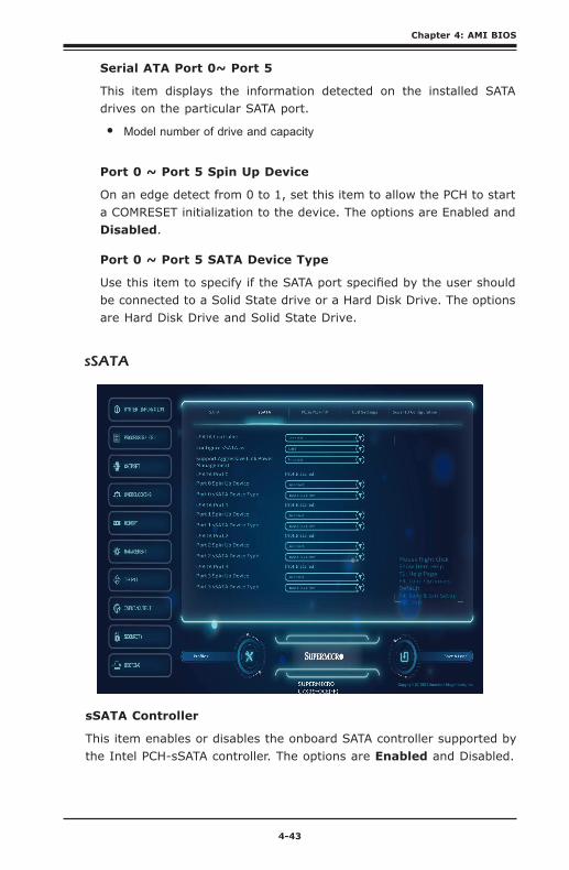
Chapter 4: AMI BIOS
4-43
Serial ATA Port 0~ Port 5
This item displays the information detected on the installed SATA drives on the particular SATA port.
• Model number of drive and capacity
Port 0 ~ Port 5 Spin Up Device
On an edge detect from 0 to 1, set this item to allow the PCH to start a COMRESET initialization to the device. The options are Enabled and Disabled.
Port 0 ~ Port 5 SATA Device Type
Use this item to specify if the SATA port specified by the user should be connected to a Solid State drive or a Hard Disk Drive. The options are Hard Disk Drive and Solid State Drive.
sSATA
sSATA Controller
This item enables or disables the onboard SATA controller supported by the Intel PCH-sSATA controller. The options are Enabled and Disabled.
4-44
Supermicro C7X99-OCE Motherboard User’s Manual
Configure sSATA as
Select IDE to configure an sSATA drive specified by the user as an IDE drive. Select AHCI to configure an sSATA drive specified by the user as an AHCI drive. The options are IDE, AHCI and RAID.
*If the item above "Configure sSATA as" is set to AHCI, the following items will display:
Support Aggressive Link Power Management
When this item is set to Enabled, the sSATA AHCI controller manages the power usage of the sSATA link. The controller will put the link to a low power state when the I/O is inactive for an extended period of time, and the power state will return to normal when the I/O becomes active. The options are Enabled and Disabled.
sSATA Port 0~ Port 3
This item displays the information detected on the installed on the sSATA port. specified by the user.
• Model number of drive and capacity
• Software Preserve Support
sSATA Port 0~ Port 3
Select Enabled to enable an sSATA port specified by the user. The options are Disabled and Enabled.
sSATA Port 0 ~ Port 3 Spin Up Device
On an edge detect from 0 to 1, set this item to allow the PCH to start a COMRESET initialization to the device. The options are Enabled and Disabled.
Port 0 ~ Port 3 sSATA Device Type
Use this item to specify if the sSATA port specified by the user should be connected to a Solid State drive or a Hard Disk Drive. The options are Hard Disk Drive and Solid State Drive.
*If the item above "Configure sSATA as" is set to IDE, the following items will display:
sSATA Port 0~ Port 3
This item indicates that an sSATA port specified by the user is installed (present) or not.
Chapter 4: AMI BIOS
4-45
Port 0 ~ Port 3 sSATA Device Type (Available when a SATA port is detected)
Use this item to specify if the sSATA port specified by the user should be connected to a Solid State drive or a Hard Disk Drive. The options are Hard Disk Drive and Solid State Drive.
PCIe/PCI/PnP
Above 4G Decoding (Available if the system supports 64-bit PCI decoding)
Select Enabled to decode a PCI device that supports 64-bit in the space above 4G Address. The options are Enabled and Disabled.
SR-IOV Support
Single Root I/O Virtualization (SR-IOV) is a specification that allows a PCIe device to appear as multiple physical devices to the system. The options are Disabled and Enabled.
CPU SLOT1 PCI-E 3.0 X8 (IN X16) BIFURCATION
This option allows the user to electrically divide the above slot into x4x4, x8 or auto. The options are Auto, x4x4, x8.
4-46
Supermicro C7X99-OCE Motherboard User’s Manual
CPU SLOT1 PCI-E 3.0 X8 (IN X16) - Gen X
This option allows the user to electrically divide the above slot electri-cal segments.The options are Auto, Gen 1 (2.5 GT/s), Gen 2 (5 GT/s), Gen 3 (8GT/s).
SLOT2 and SLOT4 Selection
This option allows the user to select between activating Slot2 and Slot4 both at x8 OR, Slot4 at x16. The options are Slot2(x8) and Slot4(x), or Slot4(x16).
CPU SLOT2 PCI-E 3.0 X8 (IN X16) - GEN X, CPU SLOT4 PCI-E 3.0 X8 (IN X16) - GEN X,
This option allows the PCI-E Generation (GT/s) speed selection of the above slots. The options are Auto, Gen 1 (2.5 GT/s), Gen 2 (5 GT/s), Gen 3 (8GT/s).
CPU SLOT6 PCI-E 3.0 X16 - Bifurcation
This option allows the PCI-E Generation (GT/s) speed selection of the above slots. The options are Auto, x4x4x4x4, x4x4x8, x8x4x4, x8x8, and x16.
CPU SLOT6 PCI-E 3.0 X16 - Gen X
This option allows the PCI-E Generation (GT/s) speed selection of the above slots. The options are Auto, Gen 1 (2.5 GT/s), Gen 2 (5 GT/s), Gen 3 (8GT/s).
CPU SLOT1 PCI-E 3.0 X8 (IN X16) OPROM, CPU SLOT2 PCI-E 3.0 X8 (IN X16) OPROM, PCH SLOT3 PCI-E 2.0 X1 (IN X4) OPROM, CPU SLOT4 PCI-E 3.0 X8 (IN X16) OPROM, PCH SLOT5 PCI-E 2.0 X1 (IN X4) OPROM, CPU SLOT6 PCI-E 3.0 X16 OPROM
Select Disabled to deactivate the selected slot, Legacy to activate the slot in legacy mode and EFI to activate the slot in EFI mode. The options are Disabled, Legacy, and EFI.
Video Option ROM Type
For the onboard video device, select an option to select the Video Option ROM type to boot from. The options are Do Not Launch, Legacy and EFI.
Onboard LAN Option ROM Type
Select an option to enable Option ROM support to boot the computer using a network device specified by the user. The options are Disabled, Legacy and EFI.
Chapter 4: AMI BIOS
4-47
Onboard LAN1 Option ROM/Onboard LAN2 Option ROM
Select PXE (Preboot Execution Environment) to boot the computer us-ing a PXE device installed in a LAN port specified. Select Disabled to prevent system boot using a device installed in a LAN port. The options for Onboard LAN1 Option ROM are Disabled and PXE. The options for Onboard LAN2 Option ROM are Disabled and PXE.
Network Stack
This feature configures the Network Stack library for resource fetching. The options are Auto and Disabled.
ASPM Support
This feature configures the ASPM (Active State Power Management) setting for the graphics installed graphics device. The options are Auto and Disabled.
VGA Priority
Use this item to select the graphics device to be used as the primary video display for system boot. The options are Onboard VGA, CPU SLOT1 PCI-E 3.0 X8 (IN X16), CPU SLOT2 PCI-E 3.0 X8 (IN X16), PCH SLOT3 PCI-E 2.0 X1 (IN X4), CPU SLOT4 PCI-E 3.0 X8 (IN X16), PCH SLOT5 PCI-E 2.0 X1 (IN X4), and CPU SLOT6 PCI-E 3.0 X16.
4-48
Supermicro C7X99-OCE Motherboard User’s Manual
USB Settings
The following will be displayed:
• USB Devices - this displays a list of the detected USB devices.
Legacy USB Support
Select Enabled to support onboard legacy USB devices. Select Auto to disable legacy support if there are no legacy USB devices present. Select Disable to have all USB devices available for EFI applications only. The options are Enabled, Disabled and Auto.
XHCI Hand-Off
This is a work-around solution for operating systems that do not support XHCI (Extensible Host Controller Interface) hand-off. The XHCI ownership change should be claimed by the XHCI driver. The settings are Enabled and Disabled.
EHCI Hand-Off
This item is for operating systems that do not support Enhanced Host Controller Interface (EHCI) hand-off. When this item is enabled, EHCI ownership change will be claimed by the EHCI driver. The settings are Enabled and Disabled.
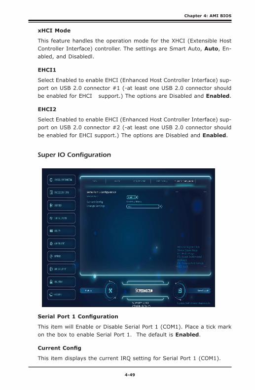
Chapter 4: AMI BIOS
4-49
xHCI Mode
This feature handles the operation mode for the XHCI (Extensible Host Controller Interface) controller. The settings are Smart Auto, Auto, En-abled, and Disabledl.
EHCI1
Select Enabled to enable EHCI (Enhanced Host Controller Interface) sup-port on USB 2.0 connector #1 (-at least one USB 2.0 connector should be enabled for EHCI support.) The options are Disabled and Enabled.
EHCI2
Select Enabled to enable EHCI (Enhanced Host Controller Interface) sup-port on USB 2.0 connector #2 (-at least one USB 2.0 connector should be enabled for EHCI support.) The options are Disabled and Enabled.
Super IO Configuration
Serial Port 1 Configuration
This item will Enable or Disable Serial Port 1 (COM1). Place a tick mark on the box to enable Serial Port 1. The default is Enabled.
Current Config
This item displays the current IRQ setting for Serial Port 1 (COM1).
4-50
Supermicro C7X99-OCE Motherboard User’s Manual
Change Settings
This item configures the IRQ setting for Serial Port 1 (COM1). The op-tions for Serial Port 1 are Auto, IO=3F8h; IRQ=4, IO=3F8h; IRQ=3, 4, 5, 6, 7, 9, 10, 11, 12, IO=2F8h; IRQ=3, 4, 5, 6, 7, 9, 10, 11, 12), IO=3E8h; IRQ=3, 4, 5, 6, 7, 9, 10, 11, 12 and IO=2E8h; IRQ=3, 4, 5, 6, 7, 9, 10, 11, 12.
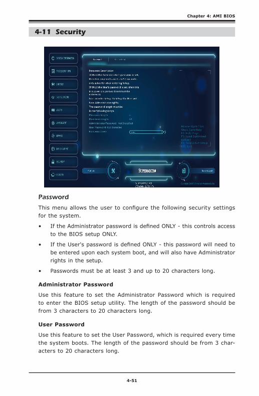
Chapter 4: AMI BIOS
4-51
4-11 Security
Password
This menu allows the user to configure the following security settings for the system.
• If the Administrator password is defined ONLY - this controls access to the BIOS setup ONLY.
• If the User's password is defined ONLY - this password will need to be entered upon each system boot, and will also have Administrator rights in the setup.
• Passwords must be at least 3 and up to 20 characters long.
Administrator Password
Use this feature to set the Administrator Password which is required to enter the BIOS setup utility. The length of the password should be from 3 characters to 20 characters long.
User Password
Use this feature to set the User Password, which is required every time the system boots. The length of the password should be from 3 char-acters to 20 characters long.
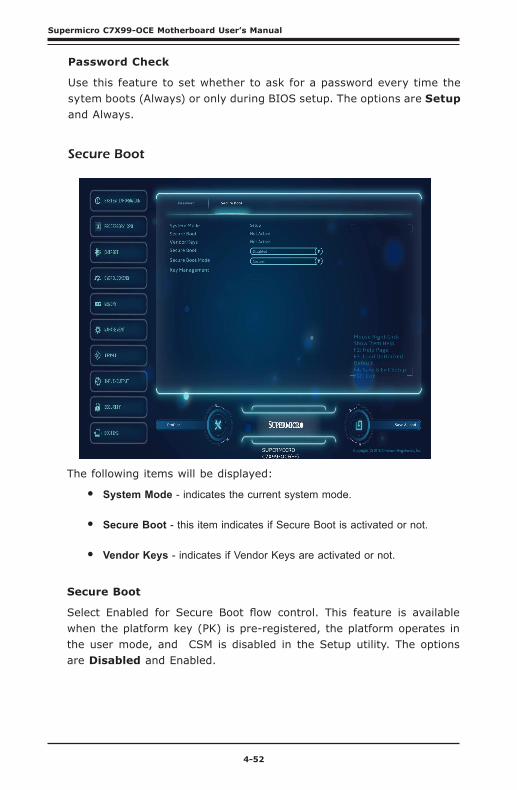
4-52
Supermicro C7X99-OCE Motherboard User’s Manual
Password Check
Use this feature to set whether to ask for a password every time the sytem boots (Always) or only during BIOS setup. The options are Setup and Always.
Secure Boot
The following items will be displayed:
• System Mode - indicates the current system mode.
• Secure Boot - this item indicates if Secure Boot is activated or not.
• Vendor Keys - indicates if Vendor Keys are activated or not.
Secure Boot
Select Enabled for Secure Boot flow control. This feature is available when the platform key (PK) is pre-registered, the platform operates in the user mode, and CSM is disabled in the Setup utility. The options are Disabled and Enabled.
Chapter 4: AMI BIOS
4-53
Secure Boot Mode
This feature allows selection of the Secure Boot Mode between Standard and Custom. Selecting Custom enables users to change the Image Ex-ecution Policy and manage Secure Boot Keys. The options are Custom and Standard.
Key Management
(if Secure Boot Mode is set to 'Custom')
Key Management allows experienced users to modify Secure Boot Vari-ables.
Default Key Provision
This item will load the default key provision. The options are Enabled and Disabled.
Enroll All Factory Default Keys
This item will install the factory default secure variables. The options are Yes and No.
Save All Secure Boot Variables
This item will save all the revised secure boot variables. The options are Yes and No.
Platform Key
This item displays the current Platform Key status.
Delete PK
This item deletes a previously installed Platform Key.
Set New PK
This item uploads and installs a secure Platform Key. You may insert a factory default key or load from a file. The file formats accepted are: 1) Public Key Certificate
a. EFI Signature List
b. EFI CERT X509 (DER Encoded)
c. EFI CERT RSA2048 (bin)
d. EFI SERT SHA256 (bin)
2) EFI Time Based Authenticated Variable
When prompted, select "Yes" to load Factory Defaults or "No' to load from a file.
4-54
Supermicro C7X99-OCE Motherboard User’s Manual
Key Exchange Key
This item displays the current Key Exchange Key status.
Delete KEK
This item deletes a previously installed Key Exchange Key.
Set New KEK
This item uploads and installs a Key Exchange Key. You may insert a factory default key or load from a file. When prompted, select "Yes" to load Factory Defaults or "No' to load from a file.
Append KEK
This item uploads and adds a Key Exchange Key into the Key Manage-ment. You may insert a factory default key or load from a file. When prompted, select "Yes" to load Factory Defaults or "No' to load from a file.
Authorized Signatures
This item displays the current Authorized Signatures status.
Delete DBT
This item deletes a previously installed Authorized Signature.
Set New DBT
This item uploads and installs an Authorized Signature . You may insert a factory default key or load from a file. The file formats accepted are: 1) Public Key Certificate
a. EFI Signature List
b. EFI CERT X509 (DER Encoded)
c. EFI CERT RSA2048 (bin)
d. EFI SERT SHA256 (bin)
2) EFI Time Based Authenticated Variable
When prompted, select "Yes" to load Factory Defaults or "No' to load from a file.
Append DBT
This item uploads and adds an Authorized Signature into the Key Man-agement. You may insert a factory default key or load from a file. When prompted, select "Yes" to load Factory Defaults or "No' to load from a file.
Chapter 4: AMI BIOS
4-55
Forbidded Signatures
This item displays the current Forbidden Signatures status.
Delete DBX
This item deletes a previously installed Forbidden Signature.
Set New DBX
This item uploads and installs a Forbidden Signature . You may insert a factory default key or load from a file. The file formats accepted are: 1) Public Key Certificate
a. EFI Signature List
b. EFI CERT X509 (DER Encoded)
c. EFI CERT RSA2048 (bin)
d. EFI SERT SHA256 (bin)
2) EFI Time Based Authenticated Variable
When prompted, select "Yes" to load Factory Defaults or "No' to load from a file.
Append DBX
This item uploads and adds an Forbidden Signature into the Key Man-agement. You may insert a factory default key or load from a file. When prompted, select "Yes" to load Factory Defaults or "No' to load from a file.
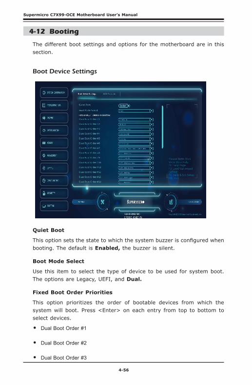
4-56
Supermicro C7X99-OCE Motherboard User’s Manual
4-12 Booting
The different boot settings and options for the motherboard are in this section.
Boot Device Settings
Quiet Boot
This option sets the state to which the system buzzer is configured when booting. The default is Enabled, the buzzer is silent.
Boot Mode Select
Use this item to select the type of device to be used for system boot. The options are Legacy, UEFI, and Dual.
Fixed Boot Order Priorities
This option prioritizes the order of bootable devices from which the system will boot. Press <Enter> on each entry from top to bottom to select devices.
• Dual Boot Order #1
• Dual Boot Order #2
• Dual Boot Order #3
Chapter 4: AMI BIOS
4-57
• Dual Boot Order #4
• Dual Boot Order #5
• Dual Boot Order #6
• Dual Boot Order #7
• Dual Boot Order #8
• Dual Boot Order #9
• Dual Boot Order #10
• Dual Boot Order #11
• Dual Boot Order #12
• Dual Boot Order #13
• Dual Boot Order #14
• Dual Boot Order #15
• HDD special boot instance
• CD/DVD special boot instance
• USB Hard Disk special boot instance
• USB CD/DVD special boot instance
• USB Key special boot instance
• USB Floppy special boot instance
• Network Special boot instance
Delete Driver Option
Use this option to delete a previously-installed driver.
Network Drive BBS Priorities
• Legacy Boot Order #1, the options are [IBA GE Slot 0500 v1404] and Disabled.
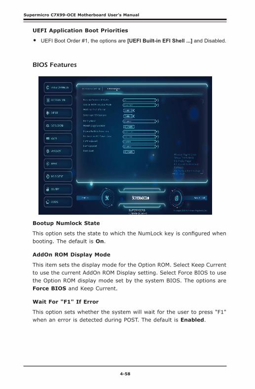
4-58
Supermicro C7X99-OCE Motherboard User’s Manual
UEFI Application Boot Priorities
• UEFI Boot Order #1, the options are [UEFI Built-in EFI Shell ...] and Disabled.
BIOS Features
Bootup Numlock State
This option sets the state to which the NumLock key is configured when booting. The default is On.
AddOn ROM Display Mode
This item sets the display mode for the Option ROM. Select Keep Current to use the current AddOn ROM Display setting. Select Force BIOS to use the Option ROM display mode set by the system BIOS. The options are Force BIOS and Keep Current.
Wait For "F1" If Error
This option sets whether the system will wait for the user to press "F1" when an error is detected during POST. The default is Enabled.
Chapter 4: AMI BIOS
4-59
Interrupt 19 Capture
Interrupt 19 is the software interrupt that handles the boot disk function. When this item is set to Enabled, the ROM BIOS of the host adaptors will "capture" Interrupt 19 at bootup and allow the drives that are attached to these host adaptors to function as bootable disks. If this item is set to Disabled, the ROM BIOS of the host adaptors will not capture Inter-rupt 19, and the drives attached to these adaptors will not function as bootable devices. The options are Enabled and Disabled.
Retry Boot
Select Enabled to force the system to reboot when system fails to boot. The options are Disabled and Enabled.
Watch Dog Function
If enabled, the Watch Dog timer will allow the system to reboot when it is unresponsive for more than 5 minutes. The default is Enabled.
Power Button Function
This feature controls how the system shuts down when the power but-ton is pressed. Select 4 Seconds Override for the user to power off the system after pressing and holding the power button for 4 seconds or longer. Select Instant Off to instantly power off the system as soon as the user presses the power button. The options are Instant Off, and 4 Seconds Override.
Restore on AC Power Loss
Use this feature to set the power state after a power outage. Select Power-Off for the system power to remain off after a power loss. Select Power-On for the system power to be turned on after a power loss. Select Last State to allow the system to resume its last power state before a power loss. The options are Last State, Power On, Stay Off.
CSM Support
This option enables the Compatibility Support Module (CSM) which per-mits the loading of a traditional OS or the use of a traditional OpROMs. The options are Enabled and Disabled.
EUP Support
EuP, or Energy Using Product is a European energy-saving specification that sets a standard on the maximum total power consumption on elec-trical products. Select Enabled to activate EUP support, select Disabled for normal S5 sleep mode (system wakeup capability).

4-60
Supermicro C7X99-OCE Motherboard User’s Manual
Fast Boot
This option sets fast system boot, quick POST, etc. The default is Dis-abled.
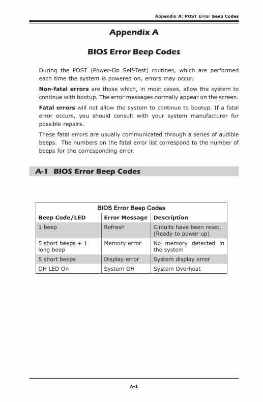
Appendix A: POST Error Beep Codes
A-1
Appendix A
BIOS Error Beep Codes
During the POST (Power-On Self-Test) routines, which are performed each time the system is powered on, errors may occur.
Non-fatal errors are those which, in most cases, allow the system to continue with bootup. The error messages normally appear on the screen.
Fatal errors will not allow the system to continue to bootup. If a fatal error occurs, you should consult with your system manufacturer for possible repairs.
These fatal errors are usually communicated through a series of audible beeps. The numbers on the fatal error list correspond to the number of beeps for the corresponding error.
A-1 BIOS Error Beep Codes
BIOS Error Beep CodesBeep Code/LED Error Message Description
1 beep Refresh Circuits have been reset. (Ready to power up)
5 short beeps + 1 long beep
Memory error No memory detected in the system
5 short beeps Display error System display error
OH LED On System OH System Overheat

A-2
Supermicro C7X99-OCE/C7X99-OCE-F Motherboard User’s Manual
Notes
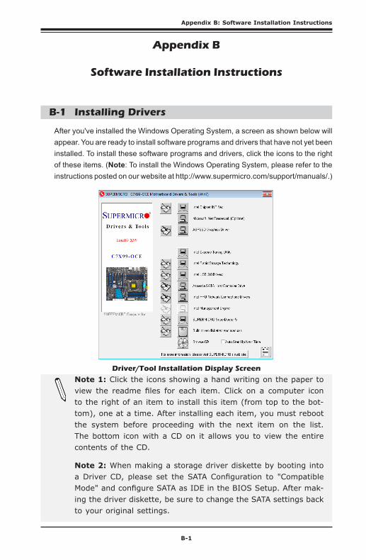
Appendix B: Software Installation Instructions
B-1
Appendix B
Software Installation Instructions
B-1 Installing Drivers
After you've installed the Windows Operating System, a screen as shown below will appear. You are ready to install software programs and drivers that have not yet been installed. To install these software programs and drivers, click the icons to the right of these items. (Note: To install the Windows Operating System, please refer to the instructions posted on our website at http://www.supermicro.com/support/manuals/.)
Driver/Tool Installation Display Screen
Note 1: Click the icons showing a hand writing on the paper to view the readme files for each item. Click on a computer icon to the right of an item to install this item (from top to the bot-tom), one at a time. After installing each item, you must reboot the system before proceeding with the next item on the list. The bottom icon with a CD on it allows you to view the entire contents of the CD.
Note 2: When making a storage driver diskette by booting into a Driver CD, please set the SATA Configuration to "Compatible Mode" and configure SATA as IDE in the BIOS Setup. After mak-ing the driver diskette, be sure to change the SATA settings back to your original settings.
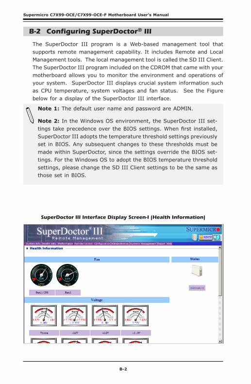
B-2
Supermicro C7X99-OCE/C7X99-OCE-F Motherboard User’s Manual
SuperDoctor III Interface Display Screen-I (Health Information)
B-2 Configuring SuperDoctor® III
The SuperDoctor III program is a Web-based management tool that supports remote management capability. It includes Remote and Local Management tools. The local management tool is called the SD III Client. The SuperDoctor III program included on the CDROM that came with your motherboard allows you to monitor the environment and operations of your system. SuperDoctor III displays crucial system information such as CPU temperature, system voltages and fan status. See the Figure below for a display of the SuperDoctor III interface.
Note 1: The default user name and password are ADMIN.
Note 2: In the Windows OS environment, the SuperDoctor III set-tings take precedence over the BIOS settings. When first installed, SuperDoctor III adopts the temperature threshold settings previously set in BIOS. Any subsequent changes to these thresholds must be made within SuperDoctor, since the settings override the BIOS set-tings. For the Windows OS to adopt the BIOS temperature threshold settings, please change the SD III Client settings to be the same as those set in BIOS.
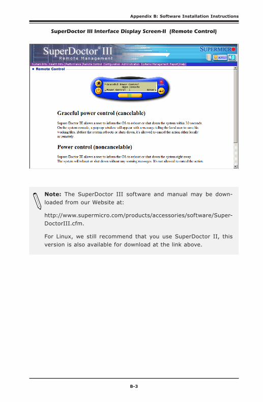
Appendix B: Software Installation Instructions
B-3
SuperDoctor III Interface Display Screen-II (Remote Control)
Note: The SuperDoctor III software and manual may be down-loaded from our Website at:
http://www.supermicro.com/products/accessories/software/Super-DoctorIII.cfm.
For Linux, we still recommend that you use SuperDoctor II, this version is also available for download at the link above.

B-4
Supermicro C7X99-OCE/C7X99-OCE-F Motherboard User’s Manual
Notes
Appendix C: UEFI BIOS Recovery
C-1
Appendix C
UEFI BIOS Recovery Instructions
Attention! Do not upgrade the BIOS unless your system has a BIOS-related issue. Flashing the wrong BIOS can cause irreparable damage to the system. In no event shall Supermicro be liable for direct, indirect, special, incidental, or consequential damages aris-ing from a BIOS update. If you need to update the BIOS, do not shut down or reset the system while the BIOS is updating to avoid possible boot failure.
C-1 An Overview to the UEFI BIOS
The Unified Extensible Firmware Interface (UEFI) specification provides a software-based interface between the operating system and the platform firmware in the pre-boot environment. The UEFI specification supports an architecture-independent mechanism for add-on card initialization to allow the UEFI OS loader, which is stored in the add-on card, to boot up the system. UEFI offers a clean, hands-off control to a computer system at bootup.
C-2 How to Recover the UEFI BIOS Image (-the Main BIOS Block)
A UEFI BIOS flash chip consists of a recovery BIOS block, comprised of two boot blocks and a main BIOS block (a main BIOS image). The boot block contains critical BIOS codes, including memory detection and recovery codes for the user to flash a new BIOS image if the original main BIOS image is corrupted. When the system power is on, the boot block codes execute first. Once that is completed, the main BIOS code will continue with system initialization and bootup.
Note: Follow the BIOS Recovery instructions below for BIOS recovery when the main BIOS boot crashes. However, when the BIOS boot block crashes, you will need to follow the procedures in Appendix D.
C-2
Supermicro C7X99-OCE/C7X99-OCE-F Motherboard User’s Manual
C-3 To Recover the Main BIOS Block Using a USB-Attached Device
This feature allows the user to recover a BIOS image using a USB-attached device without additional utilities used. A USB flash device such as a USB Flash Drive, or a USB CD/DVD ROM/RW device can be used for this purpose. However, a USB Hard Disk drive cannot be used for BIOS recovery at this time.
The file system supported by UEFI is FAT (including FAT12, FAT16, and FAT32) installed on a bootable or non-bootable USB-attached device. However, the BIOS might need several minutes to locate the SUPER.ROM file if the media size becomes too large because it contains too many folders and files.
To perform UEFI BIOS recovery using a USB-attached device, follow the instructions below.
1. Using a different machine, copy the "Super.ROM" binary image file into the disc Root "\" Directory of a USB device or a writeable CD/DVD.
Note: If you cannot locate the "SUPER.ROM" file in your driver disk, visit our website at www.supermicro.com to download the BIOS image into a USB flash device (save in the root folder) and rename it "SUPER.ROM" for BIOS recovery use.
2. Insert the USB device that contains the new BIOS image ("SUPER.ROM") into any available USB port Be sure the file is saved in the very top (root) folder.
3. Set the JBR1 switch on the motherboard to recovery mode and power on the system. If the screen appears as below, press <DEL> to continue.
Appendix C: UEFI BIOS Recovery
C-3
Note: At this point, you may decide if you want to start with BIOS Recovery. If you decide to proceed with BIOS Recovery, follow the procedures below.
5. To continue with BIOS Recovery, select the item- "Proceed with flash update". You will see the progress of BIOS Recovery as shown on the screens below.
4. After locating the new BIOS binary image, the system will enter the BIOS Recovery menu as shown below.
C-4
Supermicro C7X99-OCE/C7X99-OCE-F Motherboard User’s Manual
6. After the BIOS Recovery process is complete, click OK to reboot the system.
Note: Do not interrupt the BIOS programming until it is com-pleted.
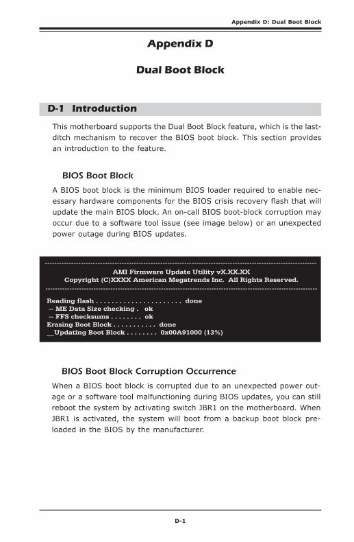
Appendix D: Dual Boot Block
D-1
Appendix D
Dual Boot Block
D-1 Introduction
This motherboard supports the Dual Boot Block feature, which is the last-ditch mechanism to recover the BIOS boot block. This section provides an introduction to the feature.
BIOS Boot Block
A BIOS boot block is the minimum BIOS loader required to enable nec-essary hardware components for the BIOS crisis recovery flash that will update the main BIOS block. An on-call BIOS boot-block corruption may occur due to a software tool issue (see image below) or an unexpected power outage during BIOS updates.
BIOS Boot Block Corruption Occurrence
When a BIOS boot block is corrupted due to an unexpected power out-age or a software tool malfunctioning during BIOS updates, you can still reboot the system by activating switch JBR1 on the motherboard. When JBR1 is activated, the system will boot from a backup boot block pre-loaded in the BIOS by the manufacturer.
-----------------------------------------------------------------------------------------------------------------AMI Firmware Update Utility vX.XX.XX
Copyright (C)XXXX American Megatrends Inc. All Rights Reserved.-----------------------------------------------------------------------------------------------------------------
Reading flash . . . . . . . . . . . . . . . . . . . . . . done -- ME Data Size checking . ok -- FFS checksums . . . . . . . . okErasing Boot Block . . . . . . . . . . . done__Updating Boot Block . . . . . . . . 0x00A91000 (13%)

D-2
Supermicro C7X99-OCE/C7X99-OCE-F Motherboard User’s Manual
D-2 Steps to Reboot the System by switch JBR1
1. Power down the system.
2. On switch JBR1 slide switch to ON, and power on the system.
3. Follow the BIOS recovery SOP listed in the previous chapter (Appendix C).
4. After completing the steps above, power down the system.
5. Turn OFF switch JBR1, and power on the system.

(Disclaimer Continued)
The products sold by Supermicro are not intended for and will not be used in life support systems, medical equipment, nuclear facilities or systems, aircraft, aircraft devices, aircraft/emergency com-munication devices or other critical systems whose failure to perform be reasonably expected to result in significant injury or loss of life or catastrophic property damage. Accordingly, Supermicro disclaims any and all liability, and should buyer use or sell such products for use in such ultra-hazardous ap-plications, it does so entirely at its own risk. Furthermore, buyer agrees to fully indemnify, defend and hold Supermicro harmless for and against any and all claims, demands, actions, litigation, and proceedings of any kind arising out of or related to such ultra-hazardous use or sale.