Embed Size (px)
Citation preview
Cadence Schematic Capture Technology
By combining schematic design capture technology, based on OrCAD® Capture, with extensive simulation and board layout technology, Cadence helps you capture design intent correctly the first time. Whether used to design a new analog circuit, revise a schematic diagram for an existing PCB, or design a digital block diagram with an HDL module, Allegro® Design Entry CIS allows designers to enter, modify, and verify connectivity for the PCB design. It also integrates with a robust Component Information System (CIS), promoting reuse of preferred compo-nents and known good-part data.
The easy-to-use technologies allow designers to focus their creativity on design capture rather than tool operation. The hierarchical schematic page editor combines a Windows user interface with functionality and features specifically for design entry tasks and for publishing design data. Centralized project manage-ment provides seamless interchange of schematic data for circuit simulation,
board layout, and signal integrity analysis. A configurable design rule check (DRC) mechanism helps eliminate costly engi-neering change orders (ECOs). A basic bill of materials (BOM) can be created from data contained in the schematic database.
Benefits
• Provides fast, intuitive schematic editing
• Boosts schematic editing efficiency through design reuse
• Automates the integration of field programmable gate arrays (FPGAs) and programmable logic devices (PLDs)
• Makes changes quickly through a single spreadsheet editor
• Imports and exports every commonly used design file format
• Integrates with a robust Component Information System (CIS) to promote reuse of preferred, current parts
Features
Schematic editing
Subcircuit reuse—without having to make multiple copies—increases schematic editing efficiency. Using hierarchical blocks, designers simply reference the same subcircuit multiple times. Automatic creation of hierar-chical ports eliminates potential design connection errors. Ports and pins can be updated dynamically for hierarchical blocks and underlying schematics. Added navigation utilities recognize block boundaries and acces-sibility using keyboard shortcuts.
Ease of use
The schematic page editor combines an intuitive user interface with functionality and features that enhance usability and speed for accomplishing design tasks and publishing design data. The autowire capability, for example, automates the often tedious and time-consuming task of wiring signal pins. Wiring between component pins is as simple as selecting a starting pin and a desti-nation pin and letting the software
To develop innovate products in narrow market windows, system designers face far greater challenges than simply capturing connectivity using schematics and sending designs into layout. They must use optimal library parts, reuse sections of previous designs to reduce risk and shorten development time, add constraints early to eliminate iterations, and perform simulation and signal integrity analysis to ensure desired operation. Cadence® schematic capture technology offers a comprehensive solution for entering, modifying, and verifying complex system designs quickly and cost-effectively.
Cadence Schematic CaptureFast, intuitive design entry with reuse of preferred, current parts
www.cadence.com 2
Cadence Schematic Capture
add the connection —all automatically and quickly. Context-sensitive menus, OLE support, custom colorization of wires/nets/parts, and a tabbed/dockable interface all provide a better user experience.
Project management
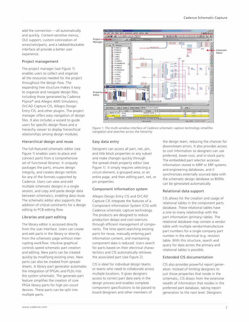
The project manager (see Figure 1) enables users to collect and organize all the resources needed for the project throughout the design flow. The expanding tree structure makes it easy to organize and navigate design files, including those generated by Cadence PSpice® and Allegro AMS Simulators, OrCAD Capture CIS, Allegro Design Entry CIS, and other plugins. The project manager offers easy navigation of design files. It also includes a wizard to guide users for specific design flows and a hierarchy viewer to display hierarchical relationships among design modules.
Hierarchical design and reuse
The full-featured schematic editor (see Figure 1) enables users to place and connect parts from a comprehensive set of functional libraries. It uniquely packages the parts, ensures design integrity, and creates design netlists for any of the formats supported by Cadence. Users can view and edit multiple schematic designs in a single session, and copy and paste design data between schematics, enabling data reuse. The schematic editor also supports the addition of critical constraints for a design editing to PCB editing flow.
Libraries and part editing
The library editor is accessed directly from the user interface. Users can create and edit parts in the library or directly from the schematic page without inter-rupting workflow. Intuitive graphical controls speed schematic part creation and editing. New parts can be created quickly by modifying existing ones. New parts can also be created from spread-sheets. A library part generator automates the integration of FPGAs and PLDs into the system schematic. The generate part feature simplifies the creation of core FPGA library parts for high pin-count devices. These parts can be split into multiple parts.
Easy data entry
Designers can access all part, net, pin, and title block properties or any subset and make changes quickly through the spread-sheet property editor (see Figure 1). It simply requires selecting a circuit element, a grouped area, or an entire page, and then editing part, net, or pin properties.
Component information system
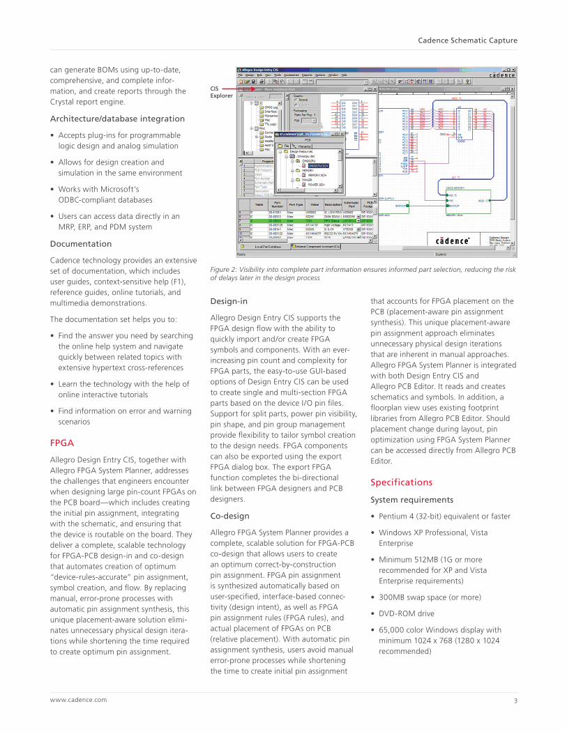
Allegro Design Entry CIS and OrCAD Capture CIS integrate the features of a Component Information System (CIS) with Cadence schematic capture technology. The products are designed to reduce production delays and cost overruns through efficient management of compo-nents. The time spent searching existing parts for reuse, manually entering part information content, and maintaining component data is reduced. Users search for parts based on their electrical charac-teristics and CIS automatically retrieves the associated part (see Figure 2).
CIS is ideal for individual design teams or teams who need to collaborate across multiple locations. It gives designers access to correct part data early in the design process and enables complete component specifications to be passed to board designers and other members of
the design team, reducing the chances for downstream errors. It also provides access to cost information so designers can use preferred, lower-cost, and in-stock parts. The embedded part selector accesses information stored in MRP or ERP systems and engineering databases, and it synchronizes externally sourced data with the schematic design database so BOMs can be generated automatically
Relational data support
CIS allows for the creation and usage of relational tables in the component parts database. These relational tables have a one-to-many relationship with the part information (primary) tables. The relational database may contain a vendor table with multiple vendor/manufacture part numbers for a single company part number in the electrical (e.g. resistor) table. With this structure, search and query for data across the primary and relational tables is possible.
Extended CIS documentation
CIS also provides powerful report gener-ation. Instead of limiting designers to just those properties that reside in the schematic, CIS draws from the extensive wealth of information that resides in the preferred part database, taking report generation to the next level. Designers
Figure 1: The multi-window interface of Cadence schematic capture technology simplifies navigation and searches across the hierarchy
ProjectManager
SchematicEditor
PropertyEditor
www.cadence.com 3
Cadence Schematic Capture
can generate BOMs using up-to-date, comprehensive, and complete infor-mation, and create reports through the Crystal report engine.
Architecture/database integration
• Accepts plug-ins for programmable logic design and analog simulation
• Allows for design creation and simulation in the same environment
• Works with Microsoft’s ODBC-compliant databases
• Users can access data directly in an MRP, ERP, and PDM system
Documentation
Cadence technology provides an extensive set of documentation, which includes user guides, context-sensitive help (F1), reference guides, online tutorials, and multimedia demonstrations.
The documentation set helps you to:
• Find the answer you need by searching the online help system and navigate quickly between related topics with extensive hypertext cross-references
• Learn the technology with the help of online interactive tutorials
• Find information on error and warning scenarios
FPGA
Allegro Design Entry CIS, together with Allegro FPGA System Planner, addresses the challenges that engineers encounter when designing large pin-count FPGAs on the PCB board—which includes creating the initial pin assignment, integrating with the schematic, and ensuring that the device is routable on the board. They deliver a complete, scalable technology for FPGA-PCB design-in and co-design that automates creation of optimum “device-rules-accurate” pin assignment, symbol creation, and flow. By replacing manual, error-prone processes with automatic pin assignment synthesis, this unique placement-aware solution elimi-nates unnecessary physical design itera-tions while shortening the time required to create optimum pin assignment.
Design-in
Allegro Design Entry CIS supports the FPGA design flow with the ability to quickly import and/or create FPGA symbols and components. With an ever-increasing pin count and complexity for FPGA parts, the easy-to-use GUI-based options of Design Entry CIS can be used to create single and multi-section FPGA parts based on the device I/O pin files. Support for split parts, power pin visibility, pin shape, and pin group management provide flexibility to tailor symbol creation to the design needs. FPGA components can also be exported using the export FPGA dialog box. The export FPGA function completes the bi-directional link between FPGA designers and PCB designers.
Co-design
Allegro FPGA System Planner provides a complete, scalable solution for FPGA-PCB co-design that allows users to create an optimum correct-by-construction pin assignment. FPGA pin assignment is synthesized automatically based on user-specified, interface-based connec-tivity (design intent), as well as FPGA pin assignment rules (FPGA rules), and actual placement of FPGAs on PCB (relative placement). With automatic pin assignment synthesis, users avoid manual error-prone processes while shortening the time to create initial pin assignment
that accounts for FPGA placement on the PCB (placement-aware pin assignment synthesis). This unique placement-aware pin assignment approach eliminates unnecessary physical design iterations that are inherent in manual approaches. Allegro FPGA System Planner is integrated with both Design Entry CIS and Allegro PCB Editor. It reads and creates schematics and symbols. In addition, a floorplan view uses existing footprint libraries from Allegro PCB Editor. Should placement change during layout, pin optimization using FPGA System Planner can be accessed directly from Allegro PCB Editor.
Specifications
System requirements
• Pentium 4 (32-bit) equivalent or faster
• Windows XP Professional, Vista Enterprise
• Minimum 512MB (1G or more recommended for XP and Vista Enterprise requirements)
• 300MB swap space (or more)
• DVD-ROM drive
• 65,000 color Windows display with minimum 1024 x 768 (1280 x 1024 recommended)
Figure 2: Visibility into complete part information ensures informed part selection, reducing the risk of delays later in the design process
CISExplorer
Cadence Schematic Capture
Cadence is transforming the global electronics industry through a vision called EDA360. With an application-driven approach to design, our software, hardware, IP, and services help customers realize silicon, SoCs, and complete systems efficiently and profitably. www.cadence.com
© 2011 Cadence Design Systems, Inc. All rights reserved. Cadence, the Cadence logo, Allegro, OrCAD, and PSpice are registered trademarks of Cadence Design Systems, Inc. All others are properties of their respective holders.
21420 11/11 MK/DM/PDF
Cadence Services and Support
• Cadence application engineers can answer your technical questions by telephone, email, or Internet—they can also provide technical assistance and custom training
• Cadence certified instructors teach more than 70 courses and bring their real-world experience into the classroom
• More than 25 Internet Learning Series (iLS) online courses allow you the flexibility of training at your own computer via the Internet
• Cadence Online Support gives you 24x7 online access to a knowledgebase of the latest solutions, technical documentation, software downloads, and more