Embed Size (px)
Citation preview
Tutorial:Layout TutorialFrom NCSU EDA Wiki
In this tutorial you will go through creating an Inverter layout while performing design-rule checks (DRC). Thistutorial assumes that you have logged in to an EOS machine and are familiar with basic UNIX commands.
Contents1 Create Aliases to Setup Your Environment2 Start the Cadence Design Framework3 Create Layout View of an Inverter
3.1 Create New Library3.2 Create New Layout View
4 Selecting and Moving Layout5 DRC
5.1 Viewing DRC Errors6 Painting7 Add Vias8 Create Pins9 Further Reading
Create Aliases to Setup Your EnvironmentBefore you start this tutorial, add the following two lines to the .mycshrc file in your home directory:
The first alias gives a command to setup your environment to run the Cadence tools. Normally, you would type"add cadence2008", but this setup adds a lot of tools we don't need, and doesn't include some that we do need.
The second alias gives a command to setup your environment to use the FreePDK45 design-kit with theCadence tools. You can set up other design-kits with other commands (such as "add cadence_cdk", which setsup the Cadence Design Kit for the MOSIS technologies).
Before moving on, either source your .mycshrc file or log out and log back in.
Note to users outside NCSU: The two scripts mentioned above are documented in thefiles $PDK_DIR/ncsu_basekit/cdssetup/icoa_setup.csh and$PDK_DIR/ncsu_basekit/cdssetup/setup.csh, respectively.
alias add_cadence2008 source /afs/eos/lockers/research/ece/wdavis/setup/ic612py425_setup.cshalias add_freepdk45 source /afs/eos/lockers/research/ece/wdavis/tech/FreePDK45/ncsu_basekit/cdssetup/setup.csh
9/23/2008 Tutorial:Layout Tutorial - NCSU EDA Wiki
http://www.eda.ncsu.edu/wiki/Tutorial:L… 1/26
Start the Cadence Design Framework1. Log in to a Linux or Solaris machine.2. Create a directory to run this tutorial, called something like "layout1". Change to this directory.3. Type "add calibre20073" at the command prompt. This will add calibre (the tool we use to run design-
rule checks) into your search path.4. Type "add_cadence2008" at the command prompt. This will add the Cadence tools to your search path.
Be sure you add this after Calibre. Otherwise, the command "add calibre" will give an error.5. Type "add_freepdk45" at the command prompt. This will setup your directory by copying in various files
that are needed to run Calibre and the Cadence tools, including .cdsinit, lib.defs, cds.lib, and.runset.calibre.drc.
6. Start the Cadence Design Framework by typing "virtuoso &" at the command prompt.
Important Note: The order in which you add cadence2008 and freepdk45 to your environment is important.Unfortunately, the scripts aren't advanced enough to be used in any order. Many students' difficulties have beensolved simply by sourcing the setup scripts in the right order.
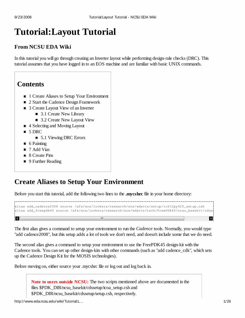
The first window that appears is called the CIW (Command Interpreter Window).
Open the library manager by selecting Tools->LibraryManager. This window allows you to browse theavailable libraries and create your own.
% add calibre20073% add_cadence2008% add_freepdk45% virtuoso &
9/23/2008 Tutorial:Layout Tutorial - NCSU EDA Wiki
http://www.eda.ncsu.edu/wiki/Tutorial:L… 2/26
Create Layout View of an Inverter
Create New Library
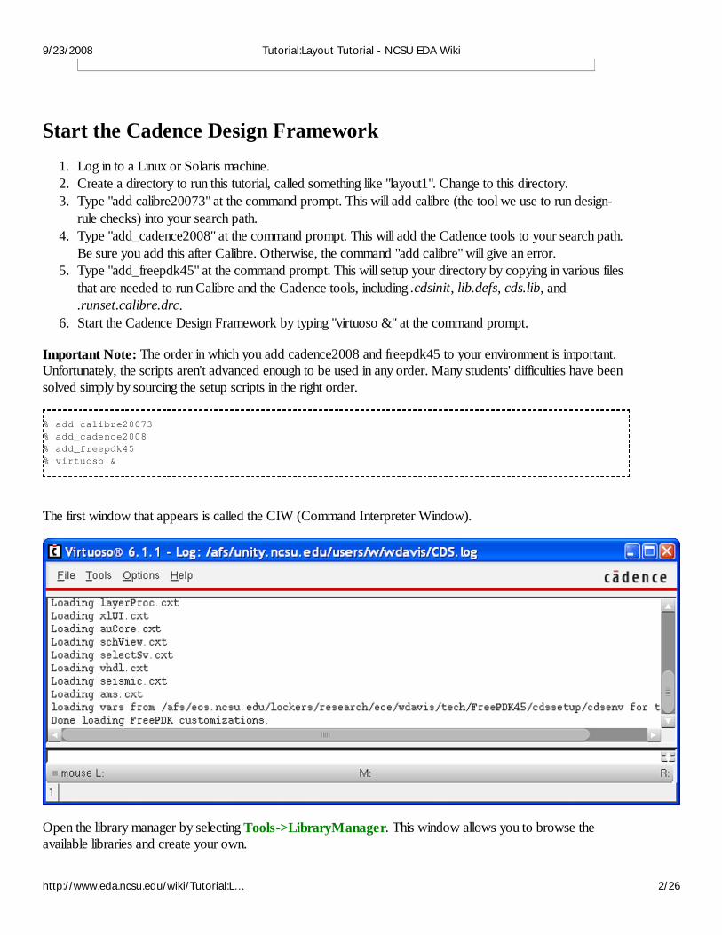
In the Library Manager, create new library called mylib. Select File->New->Library. This will open newdialog window, in which you need to enter the name and directory for your library. By default, the library will becreated in the current directory. After you fill out the form, it should look something like this:
9/23/2008 Tutorial:Layout Tutorial - NCSU EDA Wiki
http://www.eda.ncsu.edu/wiki/Tutorial:L… 3/26
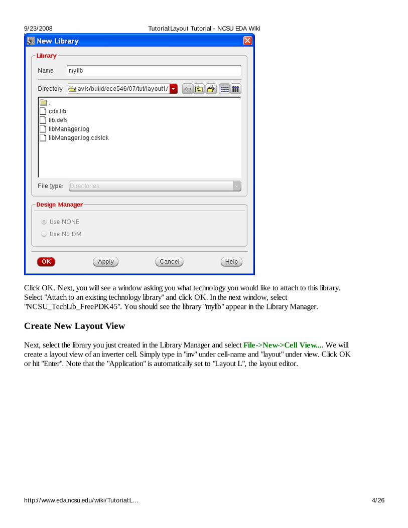
Click OK. Next, you will see a window asking you what technology you would like to attach to this library.Select "Attach to an existing technology library" and click OK. In the next window, select"NCSU_TechLib_FreePDK45". You should see the library "mylib" appear in the Library Manager.
Create New Layout View
Next, select the library you just created in the Library Manager and select File->New->Cell View.... We willcreate a layout view of an inverter cell. Simply type in "inv" under cell-name and "layout" under view. Click OKor hit "Enter". Note that the "Application" is automatically set to "Layout L", the layout editor.
9/23/2008 Tutorial:Layout Tutorial - NCSU EDA Wiki
http://www.eda.ncsu.edu/wiki/Tutorial:L… 4/26
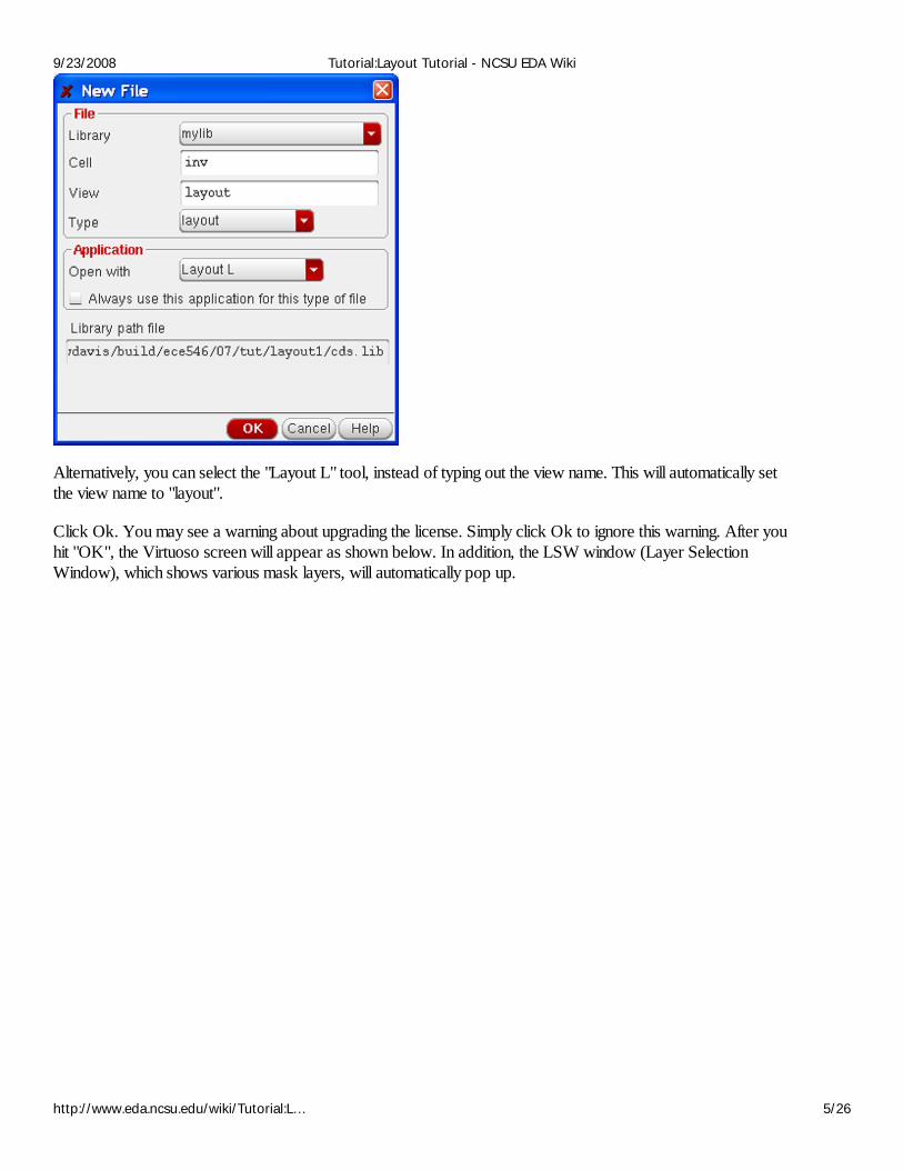
Alternatively, you can select the "Layout L" tool, instead of typing out the view name. This will automatically setthe view name to "layout".
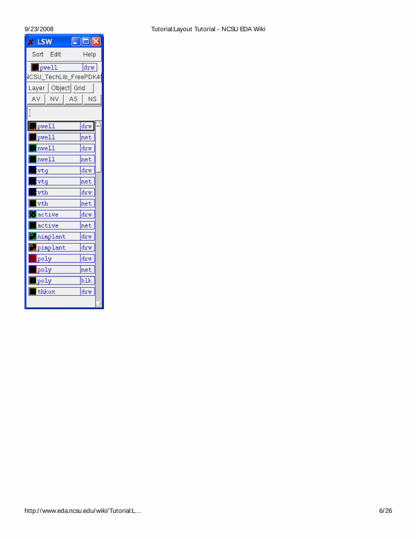
Click Ok. You may see a warning about upgrading the license. Simply click Ok to ignore this warning. After youhit "OK", the Virtuoso screen will appear as shown below. In addition, the LSW window (Layer SelectionWindow), which shows various mask layers, will automatically pop up.
9/23/2008 Tutorial:Layout Tutorial - NCSU EDA Wiki
http://www.eda.ncsu.edu/wiki/Tutorial:L… 5/26
9/23/2008 Tutorial:Layout Tutorial - NCSU EDA Wiki
http://www.eda.ncsu.edu/wiki/Tutorial:L… 6/26
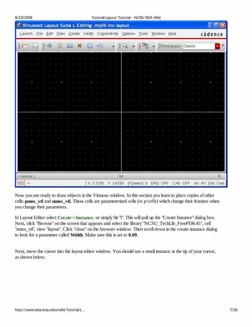
Now you are ready to draw objects in the Virtuoso window. In this section you learn to place copies of othercells: pmos_vtl and nmos_vtl. These cells are parameterized cells (or p-cells) which change their features whenyou change their parameters.
In Layout Editor select Create->Instance, or simply hit "i". This will pull up the "Create Instance" dialog box.Next, click "Browse" on the screen that appears and select the library "NCSU_TechLib_FreePDK45", cell"nmos_vtl", view "layout". Click "close" on the browser window. Then scroll down in the create-instance dialogto look for a parameter called Width. Make sure this is set to 0.09.
Next, move the cursor into the layout editor window. You should see a small instance at the tip of your cursor,as shown below.
9/23/2008 Tutorial:Layout Tutorial - NCSU EDA Wiki
http://www.eda.ncsu.edu/wiki/Tutorial:L… 7/26
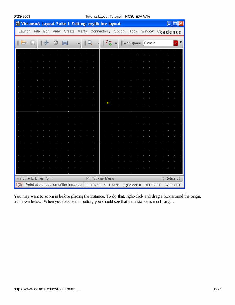
You may want to zoom in before placing the instance. To do that, right-click and drag a box around the origin,as shown below. When you release the button, you should see that the instance is much larger.
9/23/2008 Tutorial:Layout Tutorial - NCSU EDA Wiki
http://www.eda.ncsu.edu/wiki/Tutorial:L… 8/26
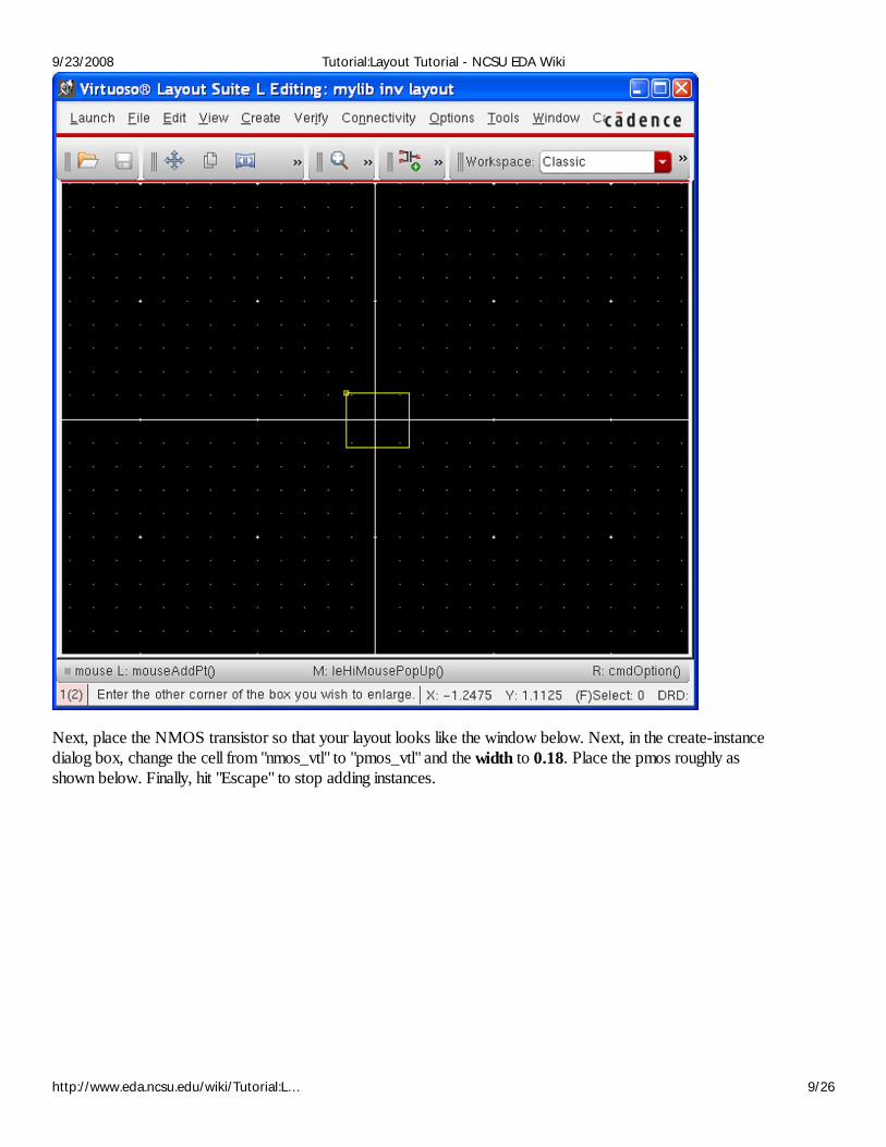
Next, place the NMOS transistor so that your layout looks like the window below. Next, in the create-instancedialog box, change the cell from "nmos_vtl" to "pmos_vtl" and the width to 0.18. Place the pmos roughly asshown below. Finally, hit "Escape" to stop adding instances.
9/23/2008 Tutorial:Layout Tutorial - NCSU EDA Wiki
http://www.eda.ncsu.edu/wiki/Tutorial:L… 9/26
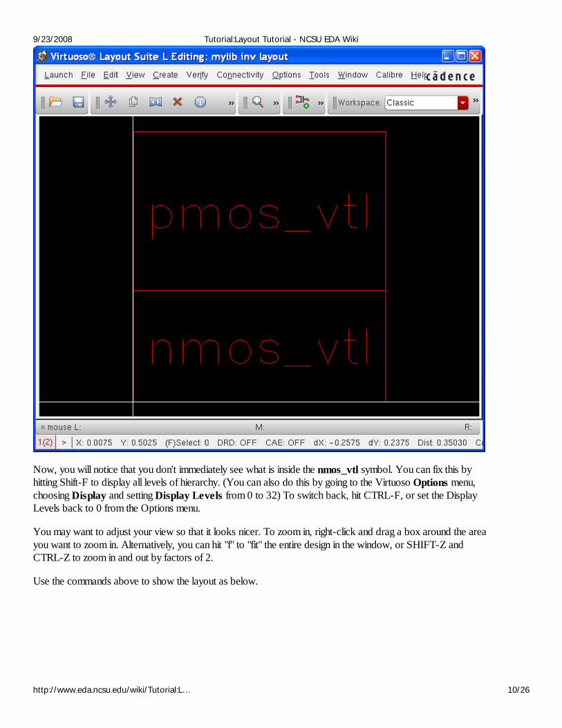
Now, you will notice that you don't immediately see what is inside the nmos_vtl symbol. You can fix this byhitting Shift-F to display all levels of hierarchy. (You can also do this by going to the Virtuoso Options menu,choosing Display and setting Display Levels from 0 to 32) To switch back, hit CTRL-F, or set the DisplayLevels back to 0 from the Options menu.
You may want to adjust your view so that it looks nicer. To zoom in, right-click and drag a box around the areayou want to zoom in. Alternatively, you can hit "f" to "fit" the entire design in the window, or SHIFT-Z andCTRL-Z to zoom in and out by factors of 2.
Use the commands above to show the layout as below.
9/23/2008 Tutorial:Layout Tutorial - NCSU EDA Wiki
http://www.eda.ncsu.edu/wiki/Tutorial:L… 10/26
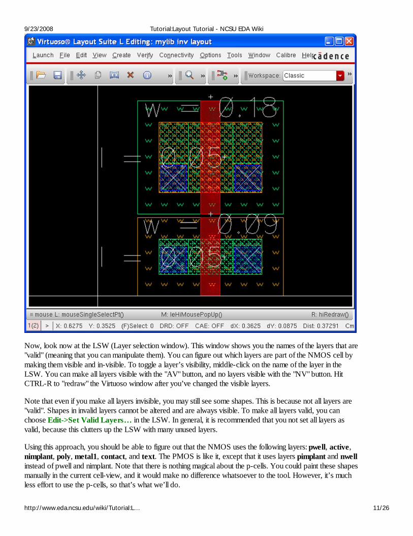
Now, look now at the LSW (Layer selection window). This window shows you the names of the layers that are"valid" (meaning that you can manipulate them). You can figure out which layers are part of the NMOS cell bymaking them visible and in-visible. To toggle a layer’s visibility, middle-click on the name of the layer in theLSW. You can make all layers visible with the "AV" button, and no layers visible with the "NV" button. HitCTRL-R to "redraw" the Virtuoso window after you’ve changed the visible layers.
Note that even if you make all layers invisible, you may still see some shapes. This is because not all layers are"valid". Shapes in invalid layers cannot be altered and are always visible. To make all layers valid, you canchoose Edit->Set Valid Layers… in the LSW. In general, it is recommended that you not set all layers asvalid, because this clutters up the LSW with many unused layers.
Using this approach, you should be able to figure out that the NMOS uses the following layers: pwell, active,nimplant, poly, metal1, contact, and text. The PMOS is like it, except that it uses layers pimplant and nwellinstead of pwell and nimplant. Note that there is nothing magical about the p-cells. You could paint these shapesmanually in the current cell-view, and it would make no difference whatsoever to the tool. However, it’s muchless effort to use the p-cells, so that’s what we’ll do.
9/23/2008 Tutorial:Layout Tutorial - NCSU EDA Wiki
http://www.eda.ncsu.edu/wiki/Tutorial:L… 11/26
Note also the letters "drw", "net", and "pin" next to each entry in the LSW. These are the purposes of a shape.The purpose is used to indicate special functionality of a shape. We will discuss these more in later tutorials. Fornow, remember that "drawing" is the purpose that indicates that a shape will appear in the mask layout. You willsometimes see "drawing" abbreviated as "drw", and sometimes "dg".
Selecting and Moving LayoutBy default, if you simply drag out a region while holding down the left mouse button (Button-1), whatever iswithin the box will be selected and highlighted in white.
Drag a box over the nmos you just instantiated. When you release the mouse button, whatever is"selected", in this case the nmos cell, will be highlighted.
Once you have selected an object (that is, an instance or a shape) you can do lots of things with it.
For example you can move it by typing the m hot-key. You can move layout up/down/left/right one grid ata time by clicking at the selection and moving the mouse. Try it.
You can also select objects by clicking on them.
Clicking the left mouse button once on an instance or shape selects it.
If you didn’t place your NMOS and PMOS cells exactly as illustrated above, try moving them now until theyare.
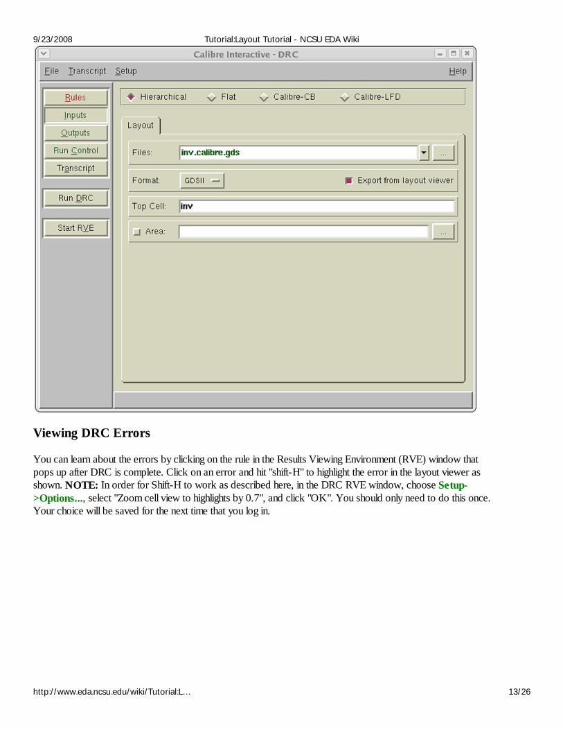
DRCTo perform a Design Rule Check (DRC), choose Calibre->Run DRC…. The DRC form appears, as shownbelow. Then click "Run DRC". If you do not see the window appear, or if you get an error, then it's possible thatyou didn't type "add calibre" as instructed above. You will need to exit Virtoso, log out, and log back in, settingup your environment in the correct order.
9/23/2008 Tutorial:Layout Tutorial - NCSU EDA Wiki
http://www.eda.ncsu.edu/wiki/Tutorial:L… 12/26
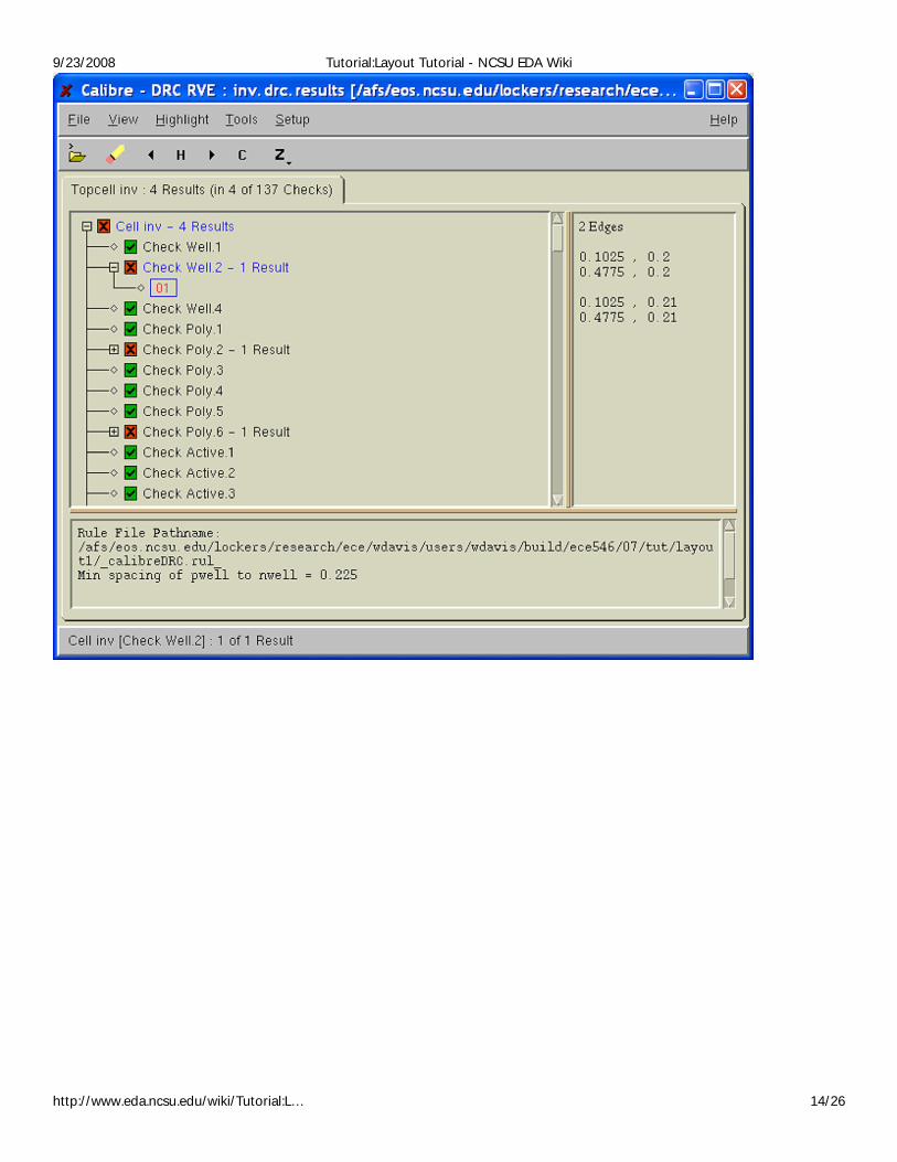
Viewing DRC Errors
You can learn about the errors by clicking on the rule in the Results Viewing Environment (RVE) window thatpops up after DRC is complete. Click on an error and hit "shift-H" to highlight the error in the layout viewer asshown. NOTE: In order for Shift-H to work as described here, in the DRC RVE window, choose Setup->Options..., select "Zoom cell view to highlights by 0.7", and click "OK". You should only need to do this once.Your choice will be saved for the next time that you log in.
9/23/2008 Tutorial:Layout Tutorial - NCSU EDA Wiki
http://www.eda.ncsu.edu/wiki/Tutorial:L… 13/26
9/23/2008 Tutorial:Layout Tutorial - NCSU EDA Wiki
http://www.eda.ncsu.edu/wiki/Tutorial:L… 14/26
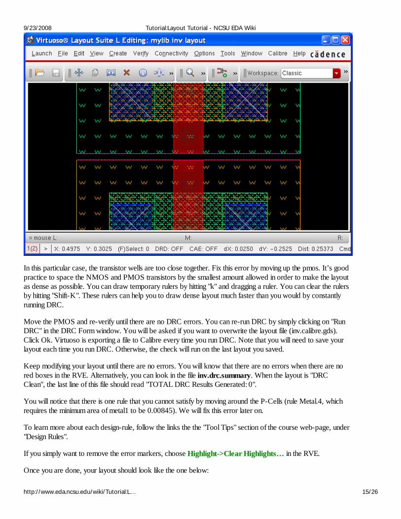
In this particular case, the transistor wells are too close together. Fix this error by moving up the pmos. It’s goodpractice to space the NMOS and PMOS transistors by the smallest amount allowed in order to make the layoutas dense as possible. You can draw temporary rulers by hitting "k" and dragging a ruler. You can clear the rulersby hitting "Shift-K". These rulers can help you to draw dense layout much faster than you would by constantlyrunning DRC.
Move the PMOS and re-verify until there are no DRC errors. You can re-run DRC by simply clicking on "RunDRC" in the DRC Form window. You will be asked if you want to overwrite the layout file (inv.calibre.gds).Click Ok. Virtuoso is exporting a file to Calibre every time you run DRC. Note that you will need to save yourlayout each time you run DRC. Otherwise, the check will run on the last layout you saved.
Keep modifying your layout until there are no errors. You will know that there are no errors when there are nored boxes in the RVE. Alternatively, you can look in the file inv.drc.summary. When the layout is "DRCClean", the last line of this file should read "TOTAL DRC Results Generated: 0".
You will notice that there is one rule that you cannot satisfy by moving around the P-Cells (rule Metal.4, whichrequires the minimum area of metal1 to be 0.00845). We will fix this error later on.
To learn more about each design-rule, follow the links the the "Tool Tips" section of the course web-page, under"Design Rules".
If you simply want to remove the error markers, choose Highlight->Clear Highlights… in the RVE.
Once you are done, your layout should look like the one below:
9/23/2008 Tutorial:Layout Tutorial - NCSU EDA Wiki
http://www.eda.ncsu.edu/wiki/Tutorial:L… 15/26
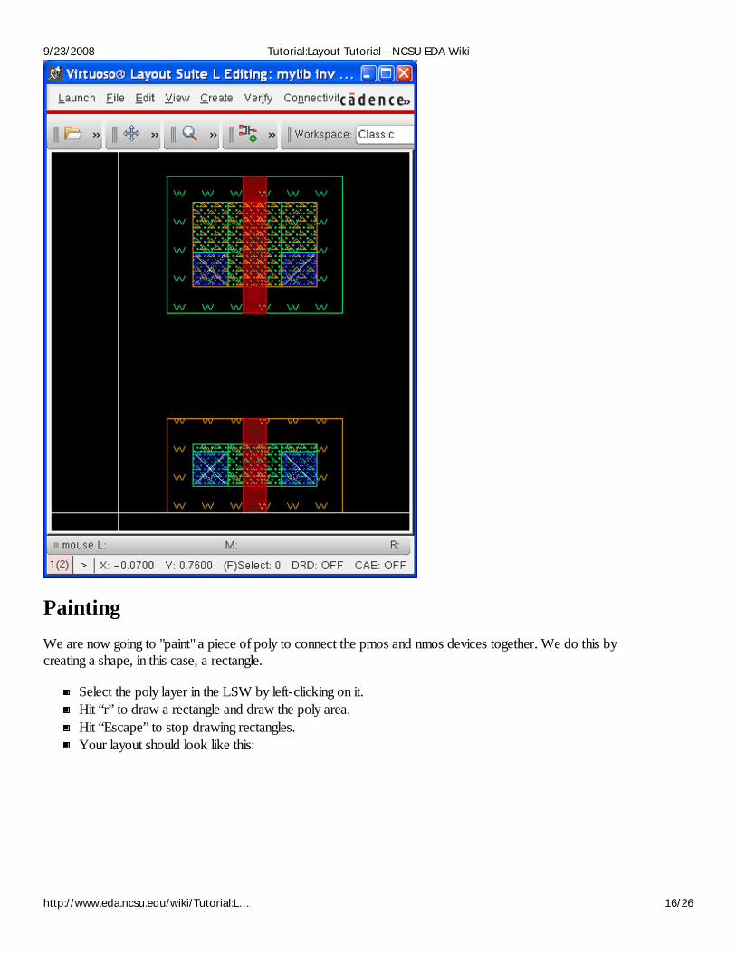
PaintingWe are now going to "paint" a piece of poly to connect the pmos and nmos devices together. We do this bycreating a shape, in this case, a rectangle.
Select the poly layer in the LSW by left-clicking on it.Hit “r” to draw a rectangle and draw the poly area.Hit “Escape” to stop drawing rectangles.Your layout should look like this:
9/23/2008 Tutorial:Layout Tutorial - NCSU EDA Wiki
http://www.eda.ncsu.edu/wiki/Tutorial:L… 16/26
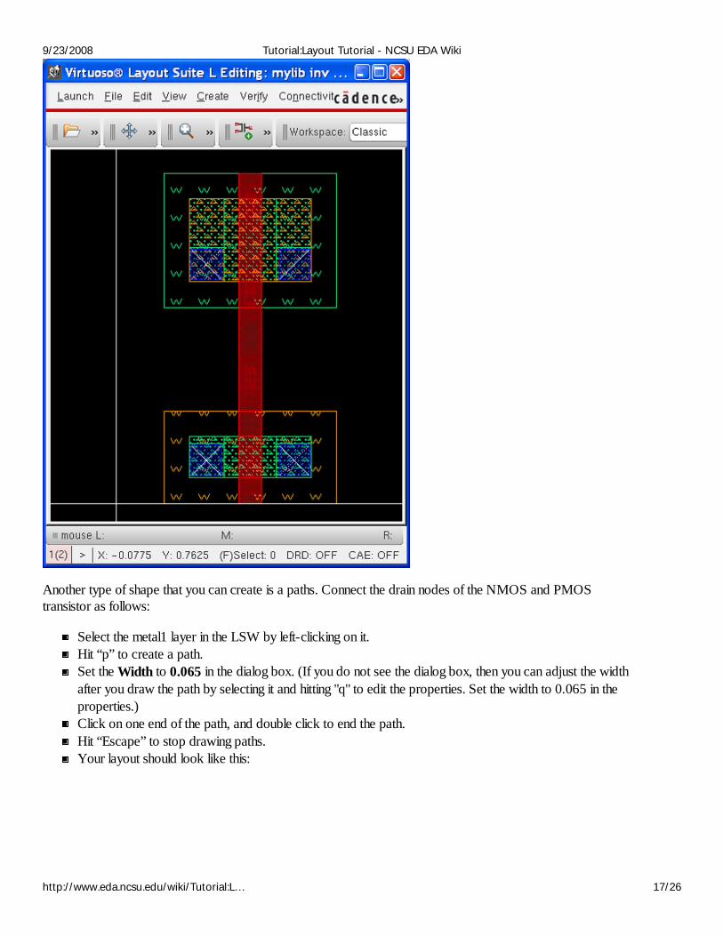
Another type of shape that you can create is a paths. Connect the drain nodes of the NMOS and PMOStransistor as follows:
Select the metal1 layer in the LSW by left-clicking on it.Hit “p” to create a path.Set the Width to 0.065 in the dialog box. (If you do not see the dialog box, then you can adjust the widthafter you draw the path by selecting it and hitting "q" to edit the properties. Set the width to 0.065 in theproperties.)Click on one end of the path, and double click to end the path.Hit “Escape” to stop drawing paths.Your layout should look like this:
9/23/2008 Tutorial:Layout Tutorial - NCSU EDA Wiki
http://www.eda.ncsu.edu/wiki/Tutorial:L… 17/26
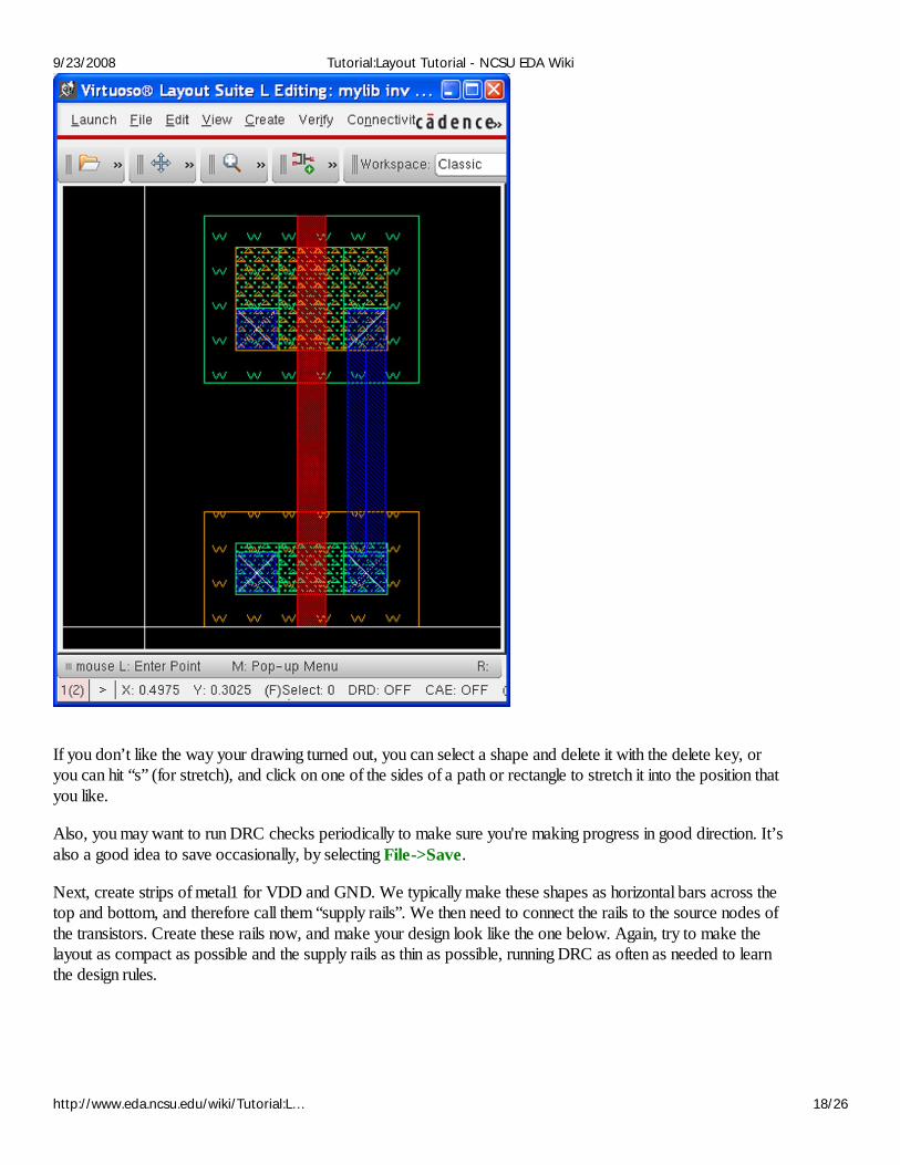
If you don’t like the way your drawing turned out, you can select a shape and delete it with the delete key, oryou can hit “s” (for stretch), and click on one of the sides of a path or rectangle to stretch it into the position thatyou like.
Also, you may want to run DRC checks periodically to make sure you're making progress in good direction. It’salso a good idea to save occasionally, by selecting File->Save.
Next, create strips of metal1 for VDD and GND. We typically make these shapes as horizontal bars across thetop and bottom, and therefore call them “supply rails”. We then need to connect the rails to the source nodes ofthe transistors. Create these rails now, and make your design look like the one below. Again, try to make thelayout as compact as possible and the supply rails as thin as possible, running DRC as often as needed to learnthe design rules.
9/23/2008 Tutorial:Layout Tutorial - NCSU EDA Wiki
http://www.eda.ncsu.edu/wiki/Tutorial:L… 18/26
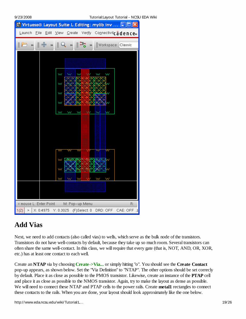
Add ViasNext, we need to add contacts (also called vias) to wells, which serve as the bulk node of the transistors.Transistors do not have well-contacts by default, because they take up so much room. Several transistors canoften share the same well-contact. In this class, we will require that every gate (that is, NOT, AND, OR, XOR,etc.) has at least one contact to each well.
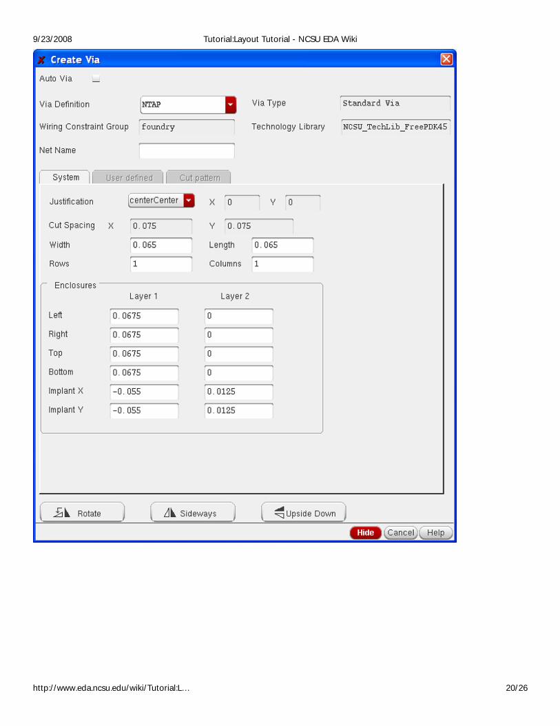
Create an NTAP via by choosing Create->Via... or simply hitting "o". You should see the Create Contactpop-up appears, as shown below. Set the "Via Definition" to "NTAP". The other options should be set correclyby default. Place it as close as possible to the PMOS transistor. Likewise, create an instance of the PTAP celland place it as close as possible to the NMOS transistor. Again, try to make the layout as dense as possible.We will need to connect these NTAP and PTAP cells to the power rails. Create metal1 rectangles to connectthese contacts to the rails. When you are done, your layout should look approximately like the one below.
9/23/2008 Tutorial:Layout Tutorial - NCSU EDA Wiki
http://www.eda.ncsu.edu/wiki/Tutorial:L… 19/26
9/23/2008 Tutorial:Layout Tutorial - NCSU EDA Wiki
http://www.eda.ncsu.edu/wiki/Tutorial:L… 20/26
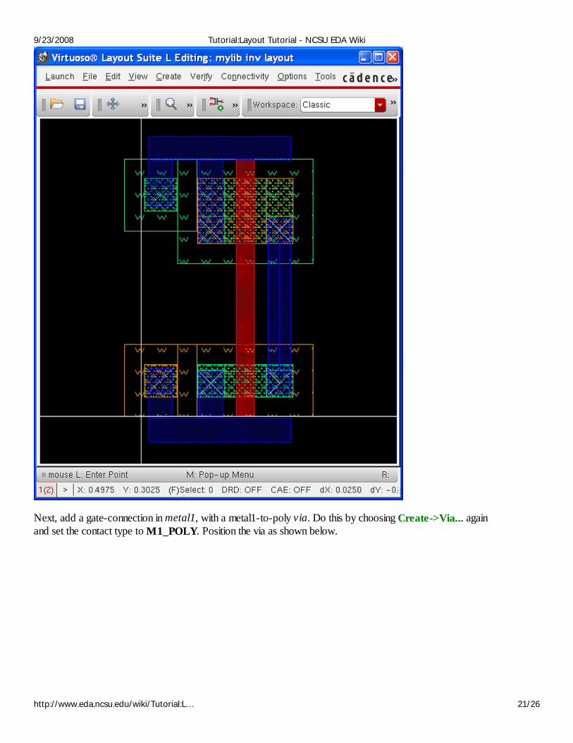
Next, add a gate-connection in metal1, with a metal1-to-poly via. Do this by choosing Create->Via... againand set the contact type to M1_POLY. Position the via as shown below.
9/23/2008 Tutorial:Layout Tutorial - NCSU EDA Wiki
http://www.eda.ncsu.edu/wiki/Tutorial:L… 21/26
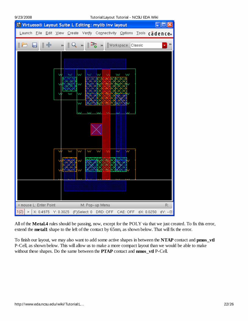
All of the Metal.4 rules should be passing, now, except for the POLY via that we just created. To fix this error,extend the metal1 shape to the left of the contact by 65nm, as shown below. That will fix the error.
To finish our layout, we may also want to add some active shapes in between the NTAP contact and pmos_vtlP-Cell, as shown below. This will allow us to make a more compact layout than we would be able to makewithout these shapes. Do the same between the PTAP contact and nmos_vtl P-Cell.
9/23/2008 Tutorial:Layout Tutorial - NCSU EDA Wiki
http://www.eda.ncsu.edu/wiki/Tutorial:L… 22/26
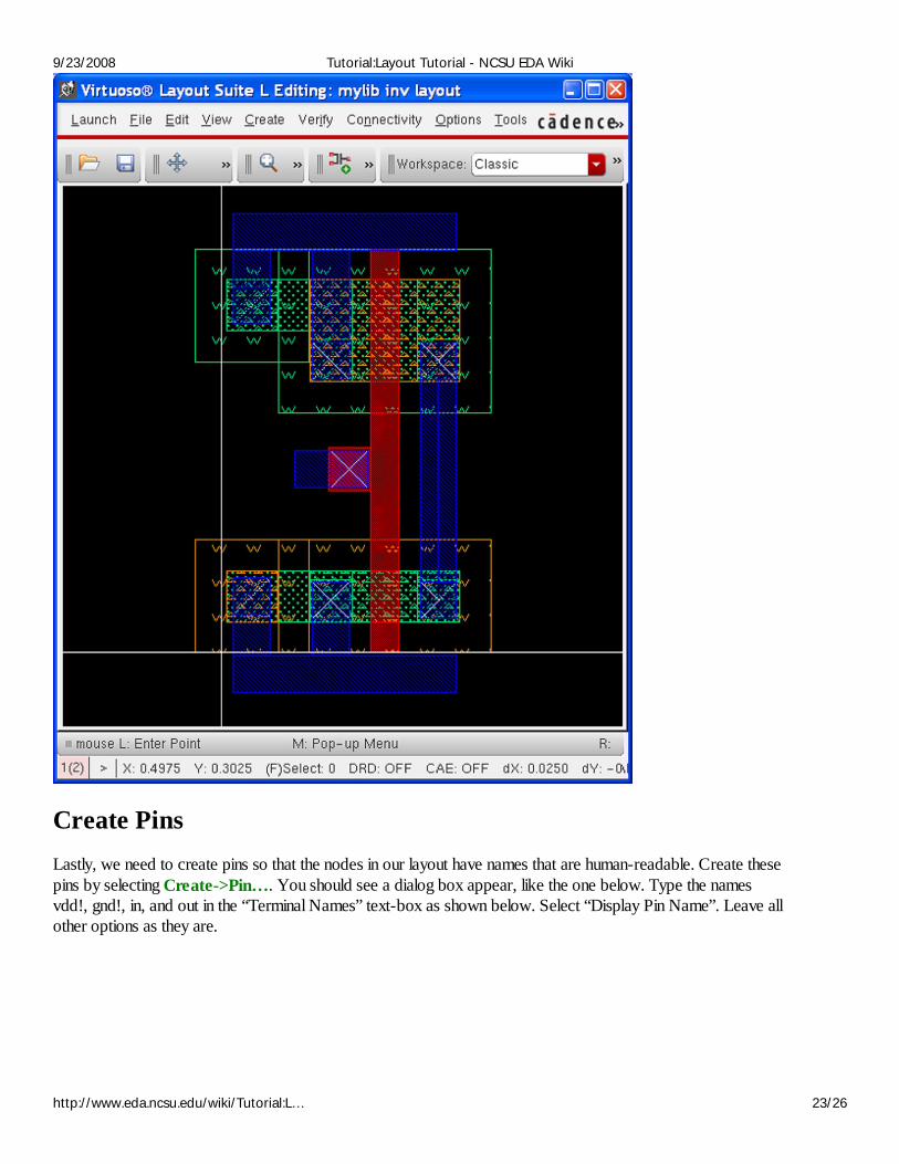
Create PinsLastly, we need to create pins so that the nodes in our layout have names that are human-readable. Create thesepins by selecting Create->Pin…. You should see a dialog box appear, like the one below. Type the namesvdd!, gnd!, in, and out in the “Terminal Names” text-box as shown below. Select “Display Pin Name”. Leave allother options as they are.
9/23/2008 Tutorial:Layout Tutorial - NCSU EDA Wiki
http://www.eda.ncsu.edu/wiki/Tutorial:L… 23/26
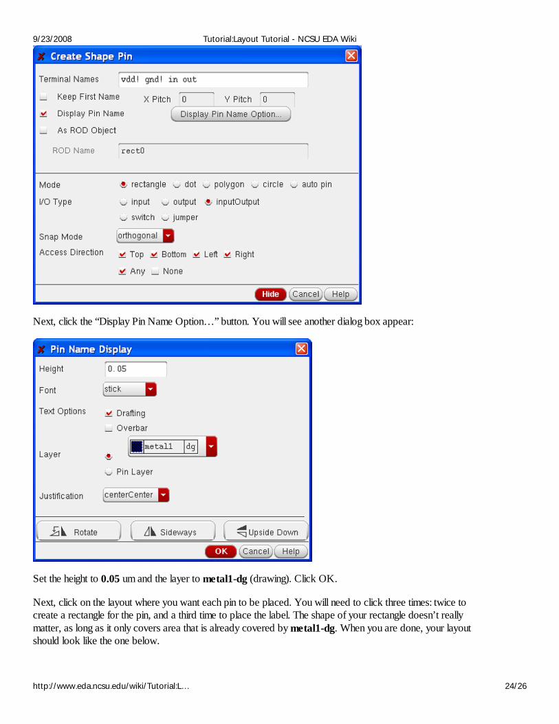
Next, click the “Display Pin Name Option…” button. You will see another dialog box appear:
Set the height to 0.05 um and the layer to metal1-dg (drawing). Click OK.
Next, click on the layout where you want each pin to be placed. You will need to click three times: twice tocreate a rectangle for the pin, and a third time to place the label. The shape of your rectangle doesn’t reallymatter, as long as it only covers area that is already covered by metal1-dg. When you are done, your layoutshould look like the one below.
9/23/2008 Tutorial:Layout Tutorial - NCSU EDA Wiki
http://www.eda.ncsu.edu/wiki/Tutorial:L… 24/26
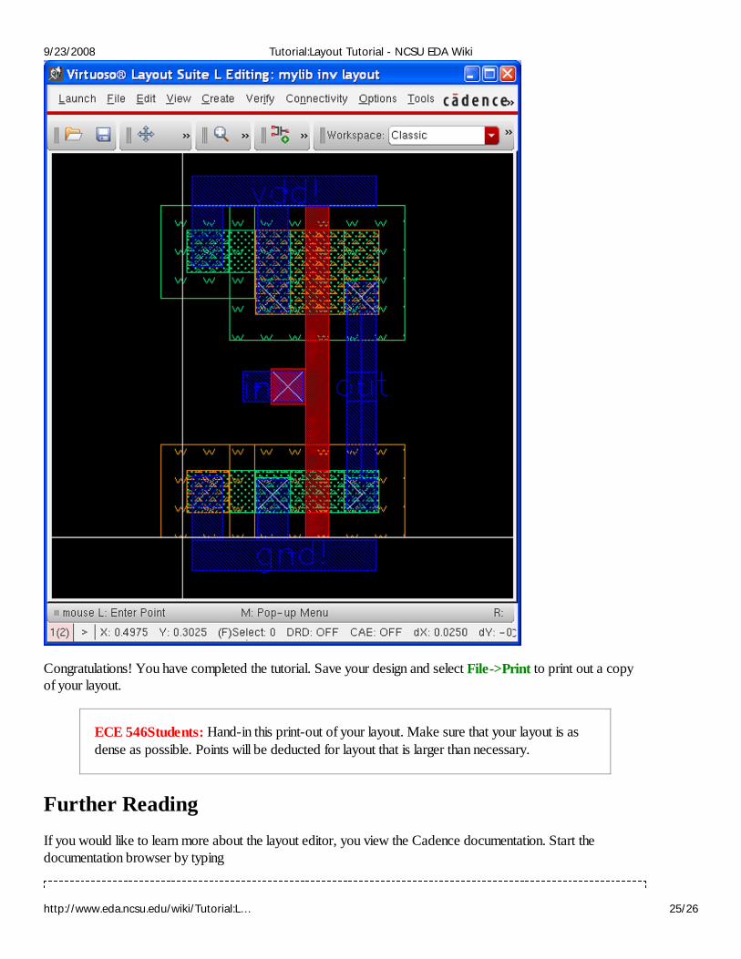
Congratulations! You have completed the tutorial. Save your design and select File->Print to print out a copyof your layout.
ECE 546Students: Hand-in this print-out of your layout. Make sure that your layout is asdense as possible. Points will be deducted for layout that is larger than necessary.
Further ReadingIf you would like to learn more about the layout editor, you view the Cadence documentation. Start thedocumentation browser by typing
9/23/2008 Tutorial:Layout Tutorial - NCSU EDA Wiki
http://www.eda.ncsu.edu/wiki/Tutorial:L… 25/26
at the command prompt, make sure that IC6.1.1 is selected in the Active Library pull-down box at the top, andthen select Virtuoso Layout Editor->Virtuoso Layout Suite L User Guide in the browser window thatappears. This should start an HTML browser that displays the table of contents for the tutorial.
If you find that you cannot view the figures correctly in the web browser, you can browse to the documentationdirectory in...
...where you will find PDF files for all of these documents. The cdsdoc documentation browser offers manymore links for you to learn about the Cadence Design Framework.
Retrieved from "http://www.eda.ncsu.edu/wiki/Tutorial:Layout_Tutorial"
This page was last modified 12:45, 1 September 2008.
cdsdoc &
/afs/eos/dist/cadence2008/ic/doc
9/23/2008 Tutorial:Layout Tutorial - NCSU EDA Wiki
http://www.eda.ncsu.edu/wiki/Tutorial:L… 26/26