Embed Size (px)
Citation preview
BNL-93721-2010-CP
Cadmium Manganese Telluride (Cd1-xMnxTe): A Potential Material for Room-Temperature
Radiation Detectors
A. Hossain, Y. Cui, A. Bolotnikov, G. Camarda, G. Yang, K-H. Kim, R. Gul, L. Xu, L. Li, A. Mycielski, and R. B. James
Presented at the 51st Annual Meeting, Institute for Nuclear Materials Management Baltimore, MD
July 11-15, 2010
June 2010
Nonproliferation and National Security Department
Brookhaven National Laboratory P.O. Box 5000
Upton, NY 11973-5000 www.bnl.gov
Notice: This manuscript has been authored by employees of Brookhaven Science Associates, LLC under Contract No. DE-AC02-98CH10886 with the U.S. Department of Energy. The publisher by accepting the manuscript for publication acknowledges that the United States Government retains a non-exclusive, paid-up, irrevocable, world-wide license to publish or reproduce the published form of this manuscript, or allow others to do so, for United States Government purposes. This preprint is intended for publication in a journal or proceedings. Since changes may be made before publication, it may not be cited or reproduced without the author’s permission.
DISCLAIMER
This report was prepared as an account of work sponsored by an agency of the United States Government. Neither the United States Government nor any agency thereof, nor any of their employees, nor any of their contractors, subcontractors, or their employees, makes any warranty, express or implied, or assumes any legal liability or responsibility for the accuracy, completeness, or any third party’s use or the results of such use of any information, apparatus, product, or process disclosed, or represents that its use would not infringe privately owned rights. Reference herein to any specific commercial product, process, or service by trade name, trademark, manufacturer, or otherwise, does not necessarily constitute or imply its endorsement, recommendation, or favoring by the United States Government or any agency thereof or its contractors or subcontractors. The views and opinions of authors expressed herein do not necessarily state or reflect those of the United States Government or any agency thereof.
CADMIUM MANGANESE TELLURIDE (Cd1-xMnxTe): A POTENTIAL MATERIAL FOR ROOM-TEMPERATURE RADIATION DETECTORS
A. Hossain1 , Y. Cui1, A. Bolotnikov1, G. Camarda1, G. Yang1, K-H. Kim1, R. Gul1, L. Xu1,2,
L. Li1, A. Mycielski3, and R. B. James1
1. Brookhaven National Laboratory, Upton, NY 11973, USA. 2. Northwestern Polytechnical University, Xi'an, Shaanxi 710072, China.
3. Institute of Physics PAS, Warsaw, Poland
ABSTRACT Cadmium Manganese Telluride (CdMnTe) recently emerged as a promising material for room-temperature X- and gamma-ray detectors. It offers several potential advantages over CdZnTe. Among them is its optimal tunable band gap ranging from 1.7-2.2 eV, and its relatively low (< 50%) content of Mn compared to that of Zn in CdZnTe that assures this favorable band-gap range. Another important asset is the segregation coefficient of Mn in CdTe that is approximately unity compared to 1.35 for Zn in CdZnTe, so ensuring the homogenous distribution of Mn throughout the ingot; hence, a large-volume stoichiometric yield is attained. However, some materials issues primarily related to the growth process impede the production of large, defect-free single crystals. The high bond-ionicity of CdMnTe entails a higher propensity to crystallize into a hexagonal structure rather than to adopt the expected zinc-blend structure, which is likely to generate twins in the crystals. In addition, bulk defects generate in the as-grown crystals due to the dearth of high-purity Mn, which yields a low-resistivity material. In this presentation, we report on our observations of such material defects in current CdMnTe materials, and our evaluation of its potential as an alternative detector material to the well-known CdZnTe detectors. We characterized the bulk defects of several indium- and vanadium-doped Cd1-xMnxTe crystals by using several advanced techniques, viz., micro-scale mapping, white-beam x-ray diffraction/reflection topography, and chemical etching. Thereafter, we fabricated some detectors from selected CdMnTe crystals, characterized their electrical properties, and tested their performance as room-temperature X- and gamma-ray detectors. Our experimental results indicate that CdMnTe materials could well prove to become a viable alternative in the near future. KEY WORDS: CdMnTe, detectors, IR microscopy, etch pit density, cellular network, mobility-lifetime product. INTRODUCTION Cadmium Manganese Telluride (CdMnTe/CMT) recently emerged as a promising material for room-temperature X- and gamma-ray detectors. It possesses several potential advantages over CdZnTe [1-4]. Among them is its tunable band-gap ranging from
Corresponding author, A. Hossain, E-mail: [email protected]
1.7-2.2 eV, resulting from its relatively low (<50%) content of Mn compared to that of Zn in CdZnTe. Another important asset is the segregation coefficient of Mn in CdTe, which approximately is unity in contrast to 1.35 for Zn in CdZnTe, so assuring the homogenous distribution of Mn throughout the ingot. However, a number of material issues primarily related to the growth processes must be resolved before CdMnTe’s successful commercialization. First, the high bond-ionicity of this material [5] entails a high propensity to crystallize into a hexagonal structure, resulting in more twinning in the crystals. To overcome this drawback, we need to optimize the Mn content in CdTe by trading off the energy band gap of CMT detector material with the adverse effects of the Mn alloying. Second, the high concentration of Cd vacancies (VCd) in as-grown crystals can result in material with very low resistivity. Compensation of such native defects by adding proper amounts of dopants (e.g., In and V) is an essential process for producing high resistivity material. In some cases the resistivity range of the ingot may still is too low for radiation-detection applications. Annealing the crystals under Cd vapor pressure is another possible compensatory measure, since it will reduce the concentration of Cd vacancies. This process significantly improves their resistivity, making them suitable for use as radiation detectors (~109-1010 Ω-cm). Hence, we undertook detailed studies with both options separately, annealing and doping, and in combination to find the appropriate parameters to produce defect-free large-volume stoichiometric CMT crystals. The scarcity of high purity source materials especially Mn is also an issue in order to obtain high quality CMT crystal. High impurity source materials generate various trapping states in the grown crystals that severely affect the material’s electrical properties. So it is essential to use high purity source materials or to purify before the crystal growth process. We have developed a special purification system and purified the Mn from 4N to 6N. In this study, all samples were selected from ingots grown by 6N grade source materials which ensured a single crystal with a relatively low concentration of impurities. We discuss our observations of the material’s extended-defects, and our evaluation of its potential as an alternative radiation detector to the well-known CZT detectors. We characterized the bulk defects of several vanadium (V) and indium (In) doped CMT crystals via several advanced techniques, viz., white-beam x-ray diffraction/reflection topography, IR transmission/reflection microscopy and chemical etching. Thereafter, we fabricated some detectors from carefully selected CMT crystals, characterized their electrical properties, and tested their performance as room-temperature X- and gamma-ray detectors. EXPERIMENTAL PROCEDURES We investigated several In- and V-doped CMT crystals; the former were as-grown, while the latter were as-grown and annealed in a Cd vapor pressure under a certain temperature and time conditions. The indium-doped samples were grown via the conventional Bridgman method with 5% Mn concentration, and the V-doped crystals were grown at 5-25% Mn concentration with a vanadium dopant concentration of 1015-1017 cm-3. All samples were mechanically polished using a 5-µm grit Al2O3 abrasive papers followed by alumina powders with decreasing levels of grit size; for the final polishing we used 0.05-µm
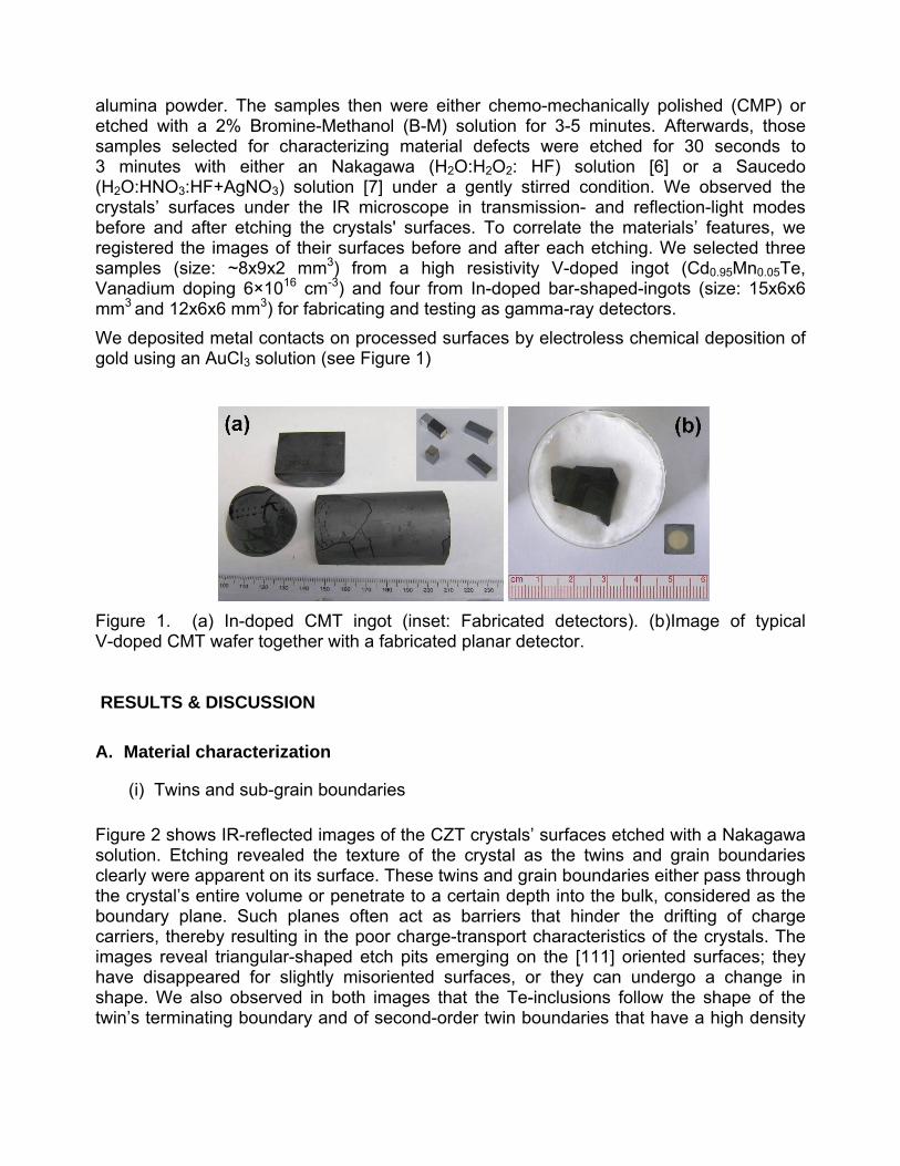
alumina powder. The samples then were either chemo-mechanically polished (CMP) or etched with a 2% Bromine-Methanol (B-M) solution for 3-5 minutes. Afterwards, those samples selected for characterizing material defects were etched for 30 seconds to 3 minutes with either an Nakagawa (H2O:H2O2: HF) solution [6] or a Saucedo (H2O:HNO3:HF+AgNO3) solution [7] under a gently stirred condition. We observed the crystals’ surfaces under the IR microscope in transmission- and reflection-light modes before and after etching the crystals' surfaces. To correlate the materials’ features, we registered the images of their surfaces before and after each etching. We selected three samples (size: ~8x9x2 mm3) from a high resistivity V-doped ingot (Cd0.95Mn0.05Te, Vanadium doping 6×1016 cm-3) and four from In-doped bar-shaped-ingots (size: 15x6x6 mm3 and 12x6x6 mm3) for fabricating and testing as gamma-ray detectors. We deposited metal contacts on processed surfaces by electroless chemical deposition of gold using an AuCl3 solution (see Figure 1)
Figure 1. (a) In-doped CMT ingot (inset: Fabricated detectors). (b)Image of typical V-doped CMT wafer together with a fabricated planar detector. RESULTS & DISCUSSION A. Material characterization
(i) Twins and sub-grain boundaries
Figure 2 shows IR-reflected images of the CZT crystals’ surfaces etched with a Nakagawa solution. Etching revealed the texture of the crystal as the twins and grain boundaries clearly were apparent on its surface. These twins and grain boundaries either pass through the crystal’s entire volume or penetrate to a certain depth into the bulk, considered as the boundary plane. Such planes often act as barriers that hinder the drifting of charge carriers, thereby resulting in the poor charge-transport characteristics of the crystals. The images reveal triangular-shaped etch pits emerging on the [111] oriented surfaces; they have disappeared for slightly misoriented surfaces, or they can undergo a change in shape. We also observed in both images that the Te-inclusions follow the shape of the twin’s terminating boundary and of second-order twin boundaries that have a high density
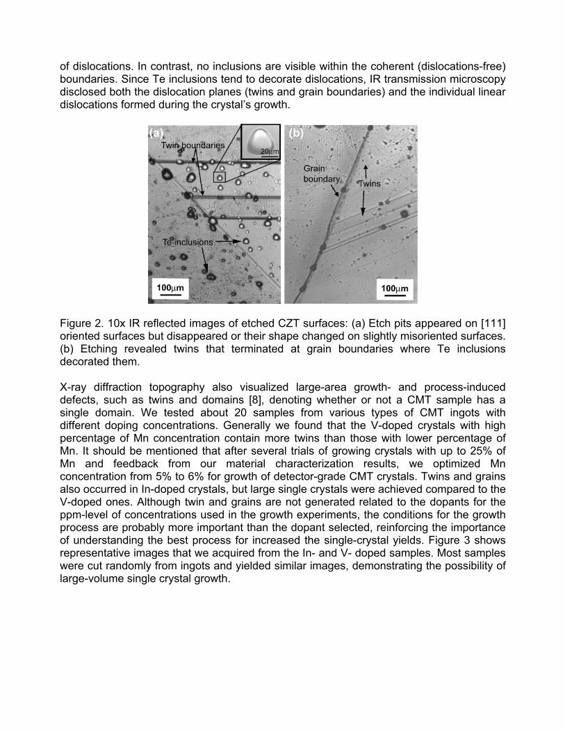
of dislocations. In contrast, no inclusions are visible within the coherent (dislocations-free) boundaries. Since Te inclusions tend to decorate dislocations, IR transmission microscopy disclosed both the dislocation planes (twins and grain boundaries) and the individual linear dislocations formed during the crystal’s growth.
Figure 2. 10x IR reflected images of etched CZT surfaces: (a) Etch pits appeared on [111] oriented surfaces but disappeared or their shape changed on slightly misoriented surfaces. (b) Etching revealed twins that terminated at grain boundaries where Te inclusions decorated them. X-ray diffraction topography also visualized large-area growth- and process-induced defects, such as twins and domains [8], denoting whether or not a CMT sample has a single domain. We tested about 20 samples from various types of CMT ingots with different doping concentrations. Generally we found that the V-doped crystals with high percentage of Mn concentration contain more twins than those with lower percentage of Mn. It should be mentioned that after several trials of growing crystals with up to 25% of Mn and feedback from our material characterization results, we optimized Mn concentration from 5% to 6% for growth of detector-grade CMT crystals. Twins and grains also occurred in In-doped crystals, but large single crystals were achieved compared to the V-doped ones. Although twin and grains are not generated related to the dopants for the ppm-level of concentrations used in the growth experiments, the conditions for the growth process are probably more important than the dopant selected, reinforcing the importance of understanding the best process for increased the single-crystal yields. Figure 3 shows representative images that we acquired from the In- and V- doped samples. Most samples were cut randomly from ingots and yielded similar images, demonstrating the possibility of large-volume single crystal growth.
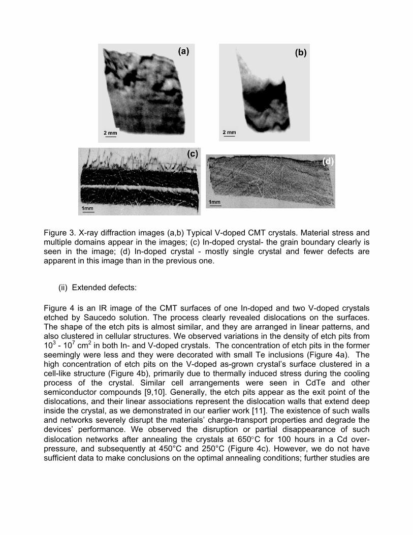
Figure 3. X-ray diffraction images (a,b) Typical V-doped CMT crystals. Material stress and multiple domains appear in the images; (c) In-doped crystal- the grain boundary clearly is seen in the image; (d) In-doped crystal - mostly single crystal and fewer defects are apparent in this image than in the previous one.
(ii) Extended defects: Figure 4 is an IR image of the CMT surfaces of one In-doped and two V-doped crystals etched by Saucedo solution. The process clearly revealed dislocations on the surfaces. The shape of the etch pits is almost similar, and they are arranged in linear patterns, and also clustered in cellular structures. We observed variations in the density of etch pits from 103 - 107 cm2 in both In- and V-doped crystals. The concentration of etch pits in the former seemingly were less and they were decorated with small Te inclusions (Figure 4a). The high concentration of etch pits on the V-doped as-grown crystal’s surface clustered in a cell-like structure (Figure 4b), primarily due to thermally induced stress during the cooling process of the crystal. Similar cell arrangements were seen in CdTe and other semiconductor compounds [9,10]. Generally, the etch pits appear as the exit point of the dislocations, and their linear associations represent the dislocation walls that extend deep inside the crystal, as we demonstrated in our earlier work [11]. The existence of such walls and networks severely disrupt the materials’ charge-transport properties and degrade the devices’ performance. We observed the disruption or partial disappearance of such dislocation networks after annealing the crystals at 650°C for 100 hours in a Cd over-pressure, and subsequently at 450°C and 250°C (Figure 4c). However, we do not have sufficient data to make conclusions on the optimal annealing conditions; further studies are
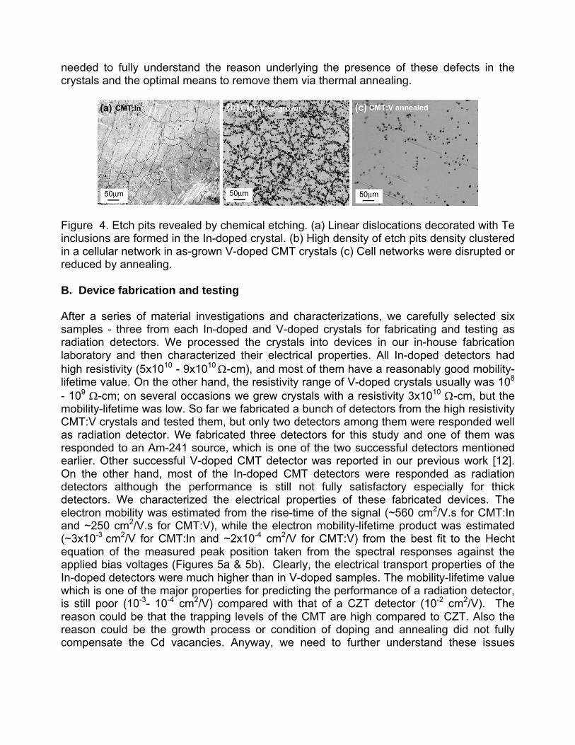
needed to fully understand the reason underlying the presence of these defects in the crystals and the optimal means to remove them via thermal annealing.
Figure 4. Etch pits revealed by chemical etching. (a) Linear dislocations decorated with Te inclusions are formed in the In-doped crystal. (b) High density of etch pits density clustered in a cellular network in as-grown V-doped CMT crystals (c) Cell networks were disrupted or reduced by annealing.
B. Device fabrication and testing After a series of material investigations and characterizations, we carefully selected six samples - three from each In-doped and V-doped crystals for fabricating and testing as radiation detectors. We processed the crystals into devices in our in-house fabrication laboratory and then characterized their electrical properties. All In-doped detectors had high resistivity (5x10¹⁰ - 9x10¹⁰ Ω-cm), and most of them have a reasonably good mobility-lifetime value. On the other hand, the resistivity range of V-doped crystals usually was 108 - 109 Ω-cm; on several occasions we grew crystals with a resistivity 3x10¹⁰ Ω-cm, but the mobility-lifetime was low. So far we fabricated a bunch of detectors from the high resistivity CMT:V crystals and tested them, but only two detectors among them were responded well as radiation detector. We fabricated three detectors for this study and one of them was responded to an Am-241 source, which is one of the two successful detectors mentioned earlier. Other successful V-doped CMT detector was reported in our previous work [12]. On the other hand, most of the In-doped CMT detectors were responded as radiation detectors although the performance is still not fully satisfactory especially for thick detectors. We characterized the electrical properties of these fabricated devices. The electron mobility was estimated from the rise-time of the signal (~560 cm2/V.s for CMT:In and ~250 cm2/V.s for CMT:V), while the electron mobility-lifetime product was estimated (~3x10⁻³ cm2/V for CMT:In and ~2x10⁻⁴ cm2/V for CMT:V) from the best fit to the Hecht equation of the measured peak position taken from the spectral responses against the applied bias voltages (Figures 5a & 5b). Clearly, the electrical transport properties of the In-doped detectors were much higher than in V-doped samples. The mobility-lifetime value which is one of the major properties for predicting the performance of a radiation detector, is still poor (10-3- 10-4 cm2/V) compared with that of a CZT detector (10-2 cm2/V). The reason could be that the trapping levels of the CMT are high compared to CZT. Also the reason could be the growth process or condition of doping and annealing did not fully compensate the Cd vacancies. Anyway, we need to further understand these issues
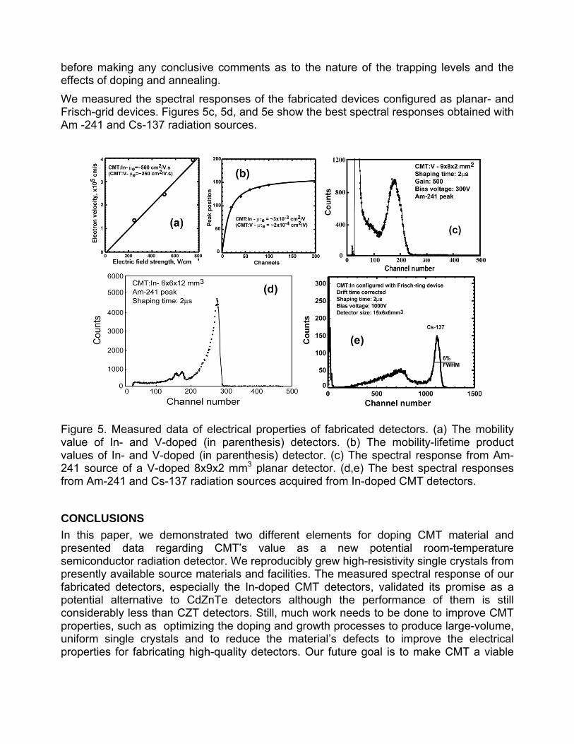
before making any conclusive comments as to the nature of the trapping levels and the effects of doping and annealing. We measured the spectral responses of the fabricated devices configured as planar- and Frisch-grid devices. Figures 5c, 5d, and 5e show the best spectral responses obtained with Am -241 and Cs-137 radiation sources.
Figure 5. Measured data of electrical properties of fabricated detectors. (a) The mobility value of In- and V-doped (in parenthesis) detectors. (b) The mobility-lifetime product values of In- and V-doped (in parenthesis) detector. (c) The spectral response from Am-241 source of a V-doped 8x9x2 mm3 planar detector. (d,e) The best spectral responses from Am-241 and Cs-137 radiation sources acquired from In-doped CMT detectors.
CONCLUSIONS
In this paper, we demonstrated two different elements for doping CMT material and presented data regarding CMT’s value as a new potential room-temperature semiconductor radiation detector. We reproducibly grew high-resistivity single crystals from presently available source materials and facilities. The measured spectral response of our fabricated detectors, especially the In-doped CMT detectors, validated its promise as a potential alternative to CdZnTe detectors although the performance of them is still considerably less than CZT detectors. Still, much work needs to be done to improve CMT properties, such as optimizing the doping and growth processes to produce large-volume, uniform single crystals and to reduce the material’s defects to improve the electrical properties for fabricating high-quality detectors. Our future goal is to make CMT a viable
alternative to CZT, so benefitting many gamma-ray or X-ray detection applications, such as nonproliferation, homeland security, and industrial / medical imaging.
ACKNOWLEDGMENT
This work was supported by U.S. Department of Energy, Office of Nonproliferation Research and Development, NA-22. The manuscript has been authored by Brookhaven Science Associates, LLC under Contract No. DE-AC02-98CH1-886 with the US Department of Energy. The United States Government retains, and the publisher, by accepting the article for publication, acknowledges, a world-wide license to publish or reproduce the published form of this manuscript, or allow others to do so, for the United States Government purposes.
REFERENCES
1. A. Burger, K. Chattopadhyay, H. Chen, J. O. Ndap, X. Ma, S. Trivedi, S. W. Kutcher, R. Chen, R. D. Resemeier, “Crystal growth, fabrication and evaluation of cadmium manganese telluride gamma ray detectors”, J. Cryst. Growth, 198-99, pp.872-876 (1999).
2. A. Mycieski, A. Burger, M. Sowinska, M. Groza, A. Szadkowski, P. Wojnar,
B. Witkowska, W. Kaliszek, and P. Siffert, “Is the (Cd,Mn)Te crystal a prospective material for X-ray and γ-ray detectors?”, Phys. Stat. Sol. (c) 2, No. 5, pp 1578-1585 (2005).
3. A. Mycielski, L. Kowalczyk, R. R. Galazka, R. Sobolewski, D. Wang, A. Burger,
M. Sowińska, M. Groza, P. Siffert, A. Szadkowski, B. Witkowska, W. Kaliszek, “Applications of II-VI semimagnetic semiconductors”, J. Alloys and Compounds, 423, pp 163-168 (2006).
4. A. Owens, and A. Peacock, “Compound semiconductor radiation detectors”, Nucl.
Instrum. & Meth. 531, pp 18-37 (2004). 5. S. Perkowitz, R. Sudharsanan, J. M. Wróbel, B. P. Clayman, and P. Becla, “Effective
charge and ionicity in Cd1-xMnxTe”, Phys. Rev. B38, pp. 5565 (1998). 6. K. Nakagawa, K. Maeda, S. Takeuchi, “Observation of dislocations in cadmium
telluride by cathodoluminescence microscopy”, Appl. Phys. Lett., 34, p. 574 (1979). 7. E. Saucedo, P. Rudolph, and E. Dieguez, “Modified Bridgman growth of CdTe
crystals”, J. Cryst. Growth 310, pp. 2067-2071 (1989).
8. G. S. Camarda, A. E. Bolotnikov, N. M. Abdul-Jabbar, S. Babalola, Y. Cui, A. Hossain, E. Jackson, H. Jackson, J. R. James, A. L. Luryi, M. Groza, A. Burger, and R. B. James, “Characterizations and measurements of CZT material: novel techniques and results”, Proc. SPIE, 6702 pp. 670605-670605-8 (2007).
9. P. Rudolph, “Fundamental studies on Bridgman growth of CdTe”,Prog. Crystal Growth
and Charact. 29 (1994) 275. 10. P. Rudolph, “Dislocation cell structures in melt-grown semiconductor compound
crystals”, Cryst. Res. Technol. 40, pp. 7-20 (2005). 11. A. Hossain, A. E. Bolotnikov, G. C. Camarda, Y. Cui, G. Yang, and R. B. James,
“Defects in Cadmium Zinc Telluride crystals revealed by etch pit distributions”, J. Cryst. Growth 310, pp. 4493-4499 (2008).
12. Y. Cui, A. E. Bolotnikov, A. Hossain, G. S. Camarda, A. Mycielski, G. Yang,
D. Kochanowska, M. Witkowska-Baran, and R. B. James, “CdMnTe in X-ray and Gamma-ray Detection: Potential Applications”, Proc. SPIE, 7079,70790N-1(2008).


![Cadmium Zinc Telluride Solar Cells by Close Spaced Sublimation[1]](https://img.pdfslide.net/doc/110x75/54fbeae64a7959434c8b52e3/cadmium-zinc-telluride-solar-cells-by-close-spaced-sublimation1.jpg)