Embed Size (px)
Citation preview

CALIBRATION OF TEVATRON IONIZATION CALIBRATION OF TEVATRON IONIZATION PROFILE MONITOR (IPM) FRONT END (FE) PROFILE MONITOR (IPM) FRONT END (FE)
MODULESMODULES
Moronkeji BandeleMoronkeji BandelePhysics and Engineering DepartmentPhysics and Engineering Department
Benedict College, Columbia, South CarolinaBenedict College, Columbia, South CarolinaSummer Internships in Science and TechnologySummer Internships in Science and Technology
Supervisor: Kwame BowieSupervisor: Kwame Bowie

August 7, 2007August 7, 2007 BandeleBandele 22
OutlineOutline Motivation Tevatron IPM DAQ System Tevatron IPM Front End (FE) Board Research Objectives Experimental Analysis
Material Preparation Initial Function Test Charge Injection Calibration Test Long – Term Stability Test
Data Analysis / Calculations Gain Plots Conclusions Future Works Acknowledgements

August 7, 2007August 7, 2007 BandeleBandele 33
MotivationMotivation A Data Acquisition (DAQ)
instrument for Tevatron
Tevatron Ionization Profile Monitor (IPM) System - to monitor the proton and antiproton beam bunch size and position at a fixed location in the Tevatron
IPM Front End (FE) Components: In – Tunnel Subsystem Upstairs Subsystem – implements
all the intelligence and control for the Tevatron IPM DAQ system.
The Tevatron and Main Injector rings

August 7, 2007August 7, 2007 BandeleBandele 44
MotivationMotivation In – tunnel Subsystem (Single Euro
Card Crate) Backplane – serves as medium for
power supply Fan – out card – duplicates signals it
receives from timing card Front – end (FE) boards – houses
the very important QIE8 chip, developed by engineers at Fermi Lab.
Upstairs Subsystem (Single PC) Timing Card – timing card sends
signals to the Euro card crate (fan – out card) on a single CAT5 cable.
Buffer Boards – stores data received
Buffer CardBuffer Card
Fan – out CardFan – out Card

August 7, 2007August 7, 2007 BandeleBandele 55
Tevatron IPM System flow chartTevatron IPM System flow chart
Host PC (Labview)
Timing card(PCI)
Data Buffer(2*8 ch)
PCI
Timingfan-out
QIE cards(16x 8 ch)
Upstairs SubsystemUpstairs Subsystem
In – tunnel SubsystemIn – tunnel Subsystem

August 7, 2007August 7, 2007 BandeleBandele 66
Tevatron IPM DAQ SystemTevatron IPM DAQ System
Computer screen
Oscilloscope
Schematic Diagram of Schematic Diagram of Experimental SetupExperimental Setup Pulse – carrying
Cable
Channel selectors
Trigger
Fan-out card
Backplane
Euro card Crate
CAT5 Cable
PC
Analog Pulse
Timing/Clock signal
Power supply
Pulse Generator
FE Boards
Bias Resistor
Optical Fiber
Oscilloscope

August 7, 2007August 7, 2007 BandeleBandele 77
Materials PreparationMaterials Preparation Solder bias resistor onto cable
Connect cable to channel selector
Insert board (s) into Euro card crate
Insert optical fiber into the optical data link
Connect CAT5 cable into PC and Euro card crate
Connect charge – carrying table to FE board
Power on the pulse generator, power supply, oscilloscope

August 7, 2007August 7, 2007 BandeleBandele 88
Material PreparationMaterial Preparation
Channel SelectorsChannel Selectors OscilloscopeOscilloscopeResistorsResistors
Power Supply systemPower Supply system FE Boards in FE Boards in Euro card crateEuro card crate
Bias resistorBias resistor soldered to cablesoldered to cable

August 7, 2007August 7, 2007 BandeleBandele 99
Tevatron IPM SystemTevatron IPM System
Actual Experimental SetupActual Experimental Setup

August 7, 2007August 7, 2007 BandeleBandele 1010
Tevatron IPM FE BoardTevatron IPM FE Board Front End portion of the IPM DAQ
system Contains the very important radiation
tolerant Application Specific Integrated Circuit (ASIC), QIE8, developed by engineers at Fermi Lab. QIE8 uses parallel circuitry to achieve a dead timeless continuous integration.
FE board functions QIE8 Chip integrates and digitizes charge
received at its input channels Generate timing and error information for
each beam bunch Transmit data to Buffer Boards via optical
link

August 7, 2007August 7, 2007 BandeleBandele 1111
Front End (FE) CardFront End (FE) CardB
AC
KP
LA
NE
QIEs,Biasing, and
Interface
PowerSupply
ClockDistribution
CircuitryQIE clock = 15 MHz
Serializer clock = 40MHz
9 Bits
9 Bits
9 Bits
9 Bits
Laser Optical Module1.6Gb/sOptical Link
9 Bits
9 Bits
9 Bits
9 Bits
Logic and ControlFPGA Module
8 Point to point PECL Clock Pairs
Header Word
Serializer
PECL
QIEclock

August 7, 2007August 7, 2007 BandeleBandele 1212
IPM FE CARD OverviewIPM FE CARD Overview1. Optical Link2. Clock Distribution3. Crystal Oscillator4. CERN GOL5. FPGA6. Analog Connectors7. QIE8 Chips8. Glue Logic9. Power Regulator10. Backplane
Connectors
6a6a
55
44
33
2211
8b8b
7a7a
7f7f
7f7f
7e7e
7d7d
7c7c
7b7b
7g7g
8c8c
8d8d
8a8a
6b6b
9a9a
9b9b
10a10a
10b10b

August 7, 2007August 7, 2007 BandeleBandele 1313
Research ObjectivesResearch Objectives
To test/calibrate the boards To collect charge data To analyze data
Testing Process Initial Functional Test Charge Injection Calibration Test : Research Focus Long Term Stability Test

August 7, 2007August 7, 2007 BandeleBandele 1414
Initial Function TestInitial Function TestInsert FE boards into Euro card crateSupply power through backplaneRun boards for five consecutive events
using Labview program; process dataMonitor closely for errors at channelsLog events in a data text fileProceed to Charge Injection Calibration
Test phase.

August 7, 2007August 7, 2007 BandeleBandele 1515
Initial Function TestInitial Function Test
Sample data logged into text fileSample data logged into text file

August 7, 2007August 7, 2007 BandeleBandele 1616
Charge Injection Calibration TestCharge Injection Calibration Test
Set and record pulse width and amplitude
Calculate expected output charge (area under pulse)
Inject charge to FE board/QIE generated by pulse generator
Run five consecutive events Read and analyze data using
Labview Software Record Pulse Peak Convert peak value from QIE
code to charge value Plot experimental results against
expected charge value
ME!ME!

August 7, 2007August 7, 2007 BandeleBandele 1717
Charge Injection Calibration TestCharge Injection Calibration Test

August 7, 2007August 7, 2007 BandeleBandele 1818
Long Term Stability TestLong Term Stability Test
Many boards are placed into Euro card crate A looping acquisition is started. The
acquisition counts the number of errors of each type on each board.
Test is run long enough to acquire enough statistics to be confident of the actual error rate.
This test is repeated with different groups of boards.

August 7, 2007August 7, 2007 BandeleBandele 1919
Long Term Stability TestLong Term Stability Test
Screenshot from the Tevatron IPM Labview programScreenshot from the Tevatron IPM Labview program
August 7, 2007August 7, 2007 BandeleBandele 2020
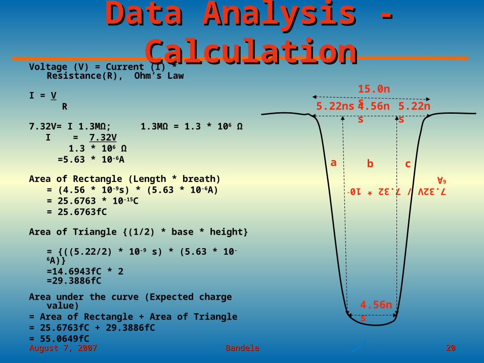
Data Analysis - CalculationData Analysis - CalculationVoltage (V) = Current (I) * Resistance(R), Ohm’s
Law
I = V R
7.32V= I 1.3MΩ; 1.3MΩ = 1.3 * 106 Ω I = 7.32V
1.3 * 106 Ω =5.63 * 10-6A
Area of Rectangle (Length * breath)
= (4.56 * 10-9s) * (5.63 * 10-6A)= 25.6763 * 10-15C= 25.6763fC
Area of Triangle {(1/2) * base * height}= {((5.22/2) * 10-9 s) * (5.63 * 10-6A)}=14.6943fC * 2=29.3886fC
Area under the curve (Expected charge value)= Area of Rectangle + Area of Triangle= 25.6763fC + 29.3886fC= 55.0649fC
7.32V / 7.32 * 10-6A
15.0ns
4.56ns
4.56ns
5.22ns5.22ns
ba c

August 7, 2007August 7, 2007 BandeleBandele 2121
Calibration Test - DataCalibration Test - DataQIE code Charge Value (fC)
43 112
44 117
45 122
46 127
47 132
48 142
49 152
50 162
51 172
52 182
53 192
54 202
55 217
56 232
57 247Conversion TableConversion Table
Screenshot from the TevatronScreenshot from the Tevatron IPM Labview programIPM Labview program

August 7, 2007August 7, 2007 BandeleBandele 2222
Calibration Test - DataCalibration Test - DataChannel 0 Channel 1 Channel 2 Channel 3 Channel 4 Channel 5 Channel 6 Channel 7
47 54 55 55 56 55 56 54
49 55 54 54 59 52 54 53
50 55 54 55 58 54 52 53
48 54 55 51 55 55 54 54
43 53 54 55 55 54 55 52
Channel 0
(fC)Channel 1
(fC)Channel 2
(fC)Channel 3
(fC)Channel 4
(fC)Channel 5
(fC)Channel 6
(fC)Channel 7
(fC)
132 202 217 217 232 217 232 202
152 217 202 202 282 182 202 192
162 217 202 217 262 202 182 192
142 202 217 172 217 217 202 202
112 192 202 217 217 202 217 182
Average 140 206 208 205 242 204 207 194
Raw Data from Lab view ProgramRaw Data from Lab view Program
Converted Data from Lab view ProgramConverted Data from Lab view Program

August 7, 2007August 7, 2007 BandeleBandele 2323
channel 0
(fC)channel 1
(fC)channel 2
(fC)channel 3
(fC)channel 4
(fC)channel 5
(fC)channel 6
(fC)channel 7
(fC)
ExpectedCharge
(fC)
15ns 140 206 208 205 242 204 207 194 55.0649
35ns 294 277 327 289 316 310 320 265 154.825
55ns 432 377 378 397 392 417 422 382 258.98
channel 0
(fC)channel 1
(fC)channel 2
(fC)channel 3
(fC)channel 4
(fC)channel 5
(fC)channel 6
(fC)channel 7
(fC)
Expected
Charge(fC)
15ns 112 139 136 137 126 136 145 122 6.59
35ns 169 175 171 156 161 173 181 167 18.59
55ns 203 199 193 186 202 199 207 194 31.08
channel 0
(fC)channel 1
(fC)channel 2
(fC)channel 3
(fC)channel 4
(fC)channel 5
(fC)channel 6
(fC)channel 7
(fC)
Expected
Charge (fC)
15ns 557 542 527 542 512 537 527 537 715.896
35ns 898 878 938 928 968 833 918 948 2013
55ns 1130 1205 1215 1200 1225 1150 1285 1245 3367.2
Calibration Test - DataCalibration Test - Data100k100kΩΩ
1M1MΩΩ
10M10MΩΩ

August 7, 2007August 7, 2007 BandeleBandele 2424
Gain Plots – Board #21Gain Plots – Board #21Board 21 - Channel 0
01000200030004000
0 200 400 600 800 1000 1200
Observed charge
Exp
ecte
d C
harg
e
Board 21 - Channel 1
0
1000
2000
3000
4000
0 500 1000 1500
Observed charge
Exp
ecte
d ch
arge
Board 21 - Channel 2
01000200030004000
0 500 1000 1500
Observed charge
Expe
cted
cha
rge
Board 21 - Channel 3
01000200030004000
0 500 1000 1500
Observed charge
Exp
ecte
d ch
arge

August 7, 2007August 7, 2007 BandeleBandele 2525
Gain Plots – Board #23Gain Plots – Board #23Board 23 - Channel 0
0
1000
2000
3000
4000
0 500 1000 1500
Observed charge
Exp
ecte
d ch
arge
Board 23 - Channel 1
0
1000
2000
3000
4000
0 100 200 300 400 500 600
Observed charge
Expe
cted
cha
rge
Board 23 - Channel 2
0
1000
2000
3000
4000
0 500 1000 1500
Observed charge
Exp
ecte
d ch
arge
Board 23 - Channel 3
0
1000
2000
3000
4000
0 200 400 600 800 1000 1200
Observed charge
Exp
ecte
d ch
arge

August 7, 2007August 7, 2007 BandeleBandele 2626
ConclusionsConclusions
Difference in readings due to the variation in the experimental setup from advised specifications for QIE8
Chip was originally designed to function at the Large Hadron Collider (LHC) at CERN
The clock integration period at which the QIE8 operates in Tevatron is 66ns (15.17MHz);should be 25ns (40MHz)
Longer clock integration time is necessary here at the Tevatron at Fermi Lab because of the difference in particle spacing
Bias resistance value of 750kΩ being used in the QIE circuitry, instead of the specified 220kΩ

August 7, 2007August 7, 2007 BandeleBandele 2727
ConclusionConclusion
Some channels on some test boards are dead
The majority of the channels have a similar linear transfer function, as expected
Most of the Front End Boards are good and can be used in Tevatron IPM Data Acquisition (DAQ) System

August 7, 2007August 7, 2007 BandeleBandele 2828
Future WorksFuture Works
There will be modifications made to several components of the channels
Boards will be re – tested until the desired result is attained

August 7, 2007August 7, 2007 BandeleBandele 2929
AcknowledgementsAcknowledgements
Almighty God
Dianne Engram
Dave Ritchie and Elliot McCrory, Mentors
Kwame Bowie – My Supervisor
Dr Davenport, Mentor
Particle Physics Division / Electrical Engineering Department Staff, 14th Floor
SIST Interns

August 7, 2007August 7, 2007 BandeleBandele 3030