Embed Size (px)
Citation preview
Outline/Agenda
Introduction
Claims & questions about coatings
Experiment design
Results of coating performance
Return on investment
Benefits and negative impact
Q & A


Properties of Nano-Coatings
Hydrophobic
Oleophobic
“Fluxophobic”

Claims About Nano-Coatings
Reduced underside cleaning
Reduced bridging
Improved solder paste release
Improved yield

Questions About Nano-Coatings
How to measure performance?
How robust are the coatings?
What is the return on investment?
What are the hidden benefits?
What are the negative impacts?

Test Procedure
1. Stencils made and nano-coated
2. Measured contact angle, abrasion
and chemical resistance
3. Printed 20 boards with no cleaning
4. Measured solder paste volume
5. Inspected bridging areas
6. Inspected underside of stencils

Experiment
Equipment and Materials
Essemtec printer
20 mm/sec, 0.18 Kg/cm, 1.5 mm/sec
ASC International SPI
AP212 with VM150 sensor
Solder paste
No clean, lead free, SAC305 Type 3
Stencils, 304 SS
0.005” (127 microns) thick Datum PhD

Experiment
Equipment and Materials
Test Board F1
Paste release in 6 BGAs
Bridging in 2 areas
0.5 mm
BGA arrays
0.4 mm
BGA arrays
Bridging
Bridging

Experiment
Equipment and Materials
BGA areas
3 x 0.5 mm arrays, SAR 0.575, 252 pads/board
3 x 0.4 mm arrays, SAR 0.500, 1080 pads/board
0.5 mm
BGA arrays
SAR 0.575
0.4 mm
BGA arrays
SAR 0.500

Experiment
Equipment and Materials
Bridging areas (2)
144 possible bridges per board
Bridging
Pitch: 8, 12, 16, 18, 20 mils

Experiment
Surface Area Ratio Calculation
0.5 mm BGA arrays
Stencil thickness = 5.0 mils (127 µm)
Aperture = 11.5 mils (292 µm) square
SAR = 0.575
0.4 mm BGA arrays
Aperture = 10.0 mils (254 µm) square
SAR = 0.500

Experiment
Stencil apertures
10.0 mil square
SAR 0.500
Printed paste
Pads on circuit board
8.0 mil round

Coating Application
Wipe on
Coating B
Coating C
Spray coat and cure
Coating A
Coating D

Coating Chemistry
Self Assembled Monolayer
Coating B
Coating C
Polymer – Cross Link
Coating A
Coating D
Stencil

Coating Thickness
Coating Thickness
Uncoated 0
Coating A 1000 – 2000 nm
(1 – 2 microns)
Coating B 2 – 4 nm
Coating C 2 – 4 nm
Coating D 2000 – 4000 nm
(2 – 4 microns)

Questions About Nano-Coatings
How to measure performance?
How robust are the coatings?
What is the return on investment?
What are the hidden benefits?
What are the negative impacts?

Performance Measurement
SURFACE FUNCTION
Contact angle
Underside cleaning
Bridging
APERTURE FUNCTION
Solder paste release
Transfer efficiency

How to Measure Contact Angle
GONIOMETER

Surface Function - Contact Angle
Hydrophobic
Surface
Hydrophilic
Surface
High Contact Angle Low
Poor Adhesiveness Good
Poor Wettability Good
Low Surface Energy High

Surface Function – Contact Angle
Coating CA
DI Water CA n-Hexadecane
Uncoated 54 9
Coating A 103 60
Coating B* 101 66
Coating C* 109 70
Coating D 105 64
*Inconsistent performance lot to lot

Performance Measurement
SURFACE FUNCTION
Contact angle
Underside cleaning
Bridging
APERTURE FUNCTION
Solder paste release
Transfer efficiency
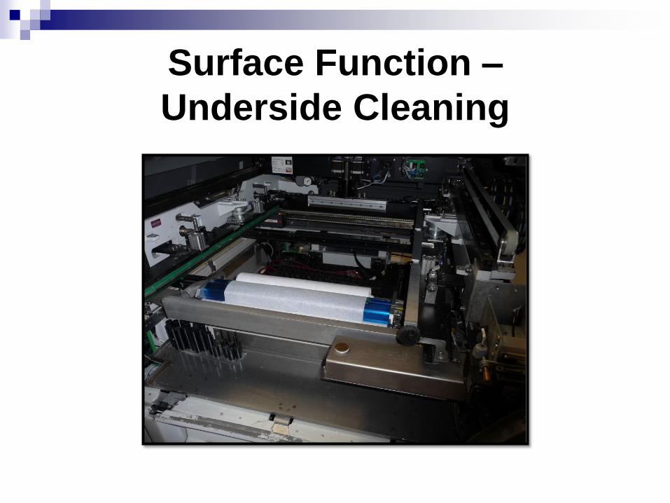
Surface Function –
Underside Cleaning

Surface Function –
Underside Cleaning
After 20 prints with no underside cleaning
Uncoated stencil Nano-coated stencil
Coatings A, B, C, D

Surface Function – Bridging
Coating Bridging
Profile
Shape
Uncoated 174 Deteriorates
Coating A 0 Consistent
Coating B 2 Consistent
Coating C 0 Consistent
Coating D 0 Consistent

Performance Measurement
SURFACE FUNCTION
Contact angle
Underside cleaning
Bridging
APERTURE FUNCTION
Solder paste release
Transfer efficiency

Aperture Function –
Solder Paste Release
Journal of SMT Volume 16 Issue 1, 2003. REAL TIME VISUALIZATION AND PREDICTION OF SOLDER PASTE
FLOW IN THE CIRCUIT BOARD PRINT OPERATION. Dr. Gerald Pham-Van-Diep, Srinivasa Aravamudhan, and
Frank Andres

Aperture Function –
Transfer Efficiency
TE by Location for SAR 0.575
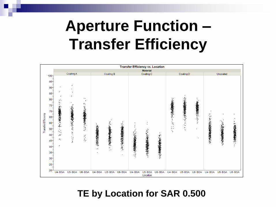
Aperture Function –
Transfer Efficiency
TE by Location for SAR 0.500

Aperture Function –
Transfer Efficiency
68
75
63 63
90
40
50
60
70
80
90
100
U A B C D
Tra
nsfe
r E
ffic
ien
cy (
%)
Coating Type
Average Transfer Efficiency SAR 0.575 (0.5 mm BGA)

Aperture Function –
Transfer Efficiency
50
67
50
42
72
30
40
50
60
70
80
90
U A B C D
Tra
nsfe
r E
ffic
ien
cy (
%)
Coating Type
Average Transfer Efficiency SAR 0.500 (0.4 mm BGA)

Aperture Function –
Stencils After 20 Prints
Coating A Coating B
Uncoated Coating D

Questions About Nano-Coatings
How to measure performance?
How robust are the coatings?
What is the return on investment?
What are the hidden benefits?
What are the negative impacts?

Robustness of Nano-Coatings
ASTM D2486 Abrasion Tester

Abrasion Test Procedure
1. Coating scrubbed for 2000 cycles
2. Contact angle measured every 500
cycles with DI water
3. Testing repeated with chemicals
added

Robustness – Abrasion
50
60
70
80
90
100
110
120
0 500 1000 1500 2000
Co
nta
ct A
ngl
e (
de
g)
Cycle Count
Abrasion - 100% Cotton
D
B
C
50
60
70
80
90
100
110
120
0 500 1000 1500 2000C
on
tact
An
gle
(d
eg)
Cycle Count
Abrasion - Water
D
B
C

Robustness –
Abrasion with Chemicals
50
60
70
80
90
100
110
120
0 500 1000 1500 2000
Co
nta
ct A
ngl
e (
de
g)
Cycle Count
Abrasion - IPA
D
B
50
60
70
80
90
100
110
120
0 500 1000 1500 2000C
on
tact
An
gle
(d
eg)
Cycle Count
Abrasion - 25% Rosin Flux
D
B
Questions About Nano-Coatings
How to measure performance?
How robust are the coatings?
What is the return on investment?
What are the hidden benefits?
What are the negative impacts?

Return on Investment
Cost of Printing
Cycle time - productivity
Cleaning material usage
Waste of solder paste
Yield loss
Rework time and materials

Return on Investment –
Cycle Time
Clean Every Print - Uncoated Stencil
Typical for small SAR <0.55
Print 1 board every 60-70 seconds
Clean Every 20 Prints - Nano-Coating
Print 1 board every 25-35 seconds
Doubles print productivity

Return on Investment –
Cleaning Material Usage
Clean Every Print – Uncoated Stencil
Fabric usage = 3 inch x $0.04/in = $0.12
Solvent usage = 10 mL x $0.008/mL = $0.08
Total = $0.20 per circuit board
Clean Every 20 Prints - Nano-Coating
Total = $0.01 per circuit board

Return on Investment –
Solder Paste Waste
Uncoated Stencil
Solder paste is cleaned from stencil bottom
0.4 to 0.7 grams of paste cleaned from stencil
Waste of $0.04 to $0.07 per board
70%
30%
Transfer Efficiency
Wasted Paste

Return on Investment –
Solder Paste Waste
Nano-Coated Stencil
Solder paste is NOT cleaned from stencil bottom
No waste of solder paste, save $$$

Return on Investment –
Yield Loss
Print Issues Account for the Majority of Defects
Nano-coating yield improvements of 10 – 70%
reported by Shea, Zubrick, and Whittier*
Increased TE can improve these defects: insufficient
solder, solder balling, graping
If a circuit board costs $100, preventing scrap pays for
most nano-coatings
*SMTA 2011, USING SPI TO IMPROVE PRINT YIELDS. C. Shea, M. Zubrick, R.
Whittier

Return on Investment –
Rework Time and Materials
What is the Impact of Nano-
Coatings on Rework?
First pass yield improvement
Eliminate rework and improve
cycle time
Save materials and labor cost

Return on Investment
Item Cost Savings ($)
Improved print cycle time 2 boards per minute instead of 1
Cleaning material savings Save $0.18 – 0.20 per board
Solder paste waste reduction Save $0.04 – 0.07 per board
Yield improvement Savings inestimable
Save on rework costs Savings inestimable
If Nano-coating costs $40 ROI is 150 to 180 boards

Questions About Nano-Coatings
How to measure performance?
How robust are the coatings?
What is the return on investment?
What are the hidden benefits?
What are the negative impacts?

Hidden Benefits
Benefits Nano-Coatings Tested
Underside cleaning improved All coatings – A, B, C, D
Bridging improved All coatings – A, B, C, D
Transfer efficiency increased Coatings A and D
Visible on the stencil Coatings A and D
Re-apply by the user Coatings B and C

Questions About Nano-Coatings
How to measure performance?
How robust are the coatings?
What is the return on investment?
What are the hidden benefits?
What are the negative impacts?

Negative Impact
Negative Impacts Nano-Coatings
Coating wears through
abrasion Coatings B and C
Coating wear not visible Coatings B and C
Transfer efficiency decreased Coatings B and C
Conclusions
Nano-coatings provide benefits, but coatings differ in
performance.
The cost of most coatings is negligible compared to
the costs of cleaning materials, solder paste waste,
defects, yield loss and rework.
If you use a nano-coating, be sure to choose the
right one.