Embed Size (px)
Citation preview
Capabilities andCapabilities and
Limitations of Limitations of Slow Light Optical Buffers:Slow Light Optical Buffers:
Searching forSearching for
the Killer Applicationthe Killer Application
Rod Tucker
ARC Special Research Centre for Ultra-Broadband Information Networks (CUBIN)Department of Electrical and Electronic Engineering
University of Melbourne, Australia
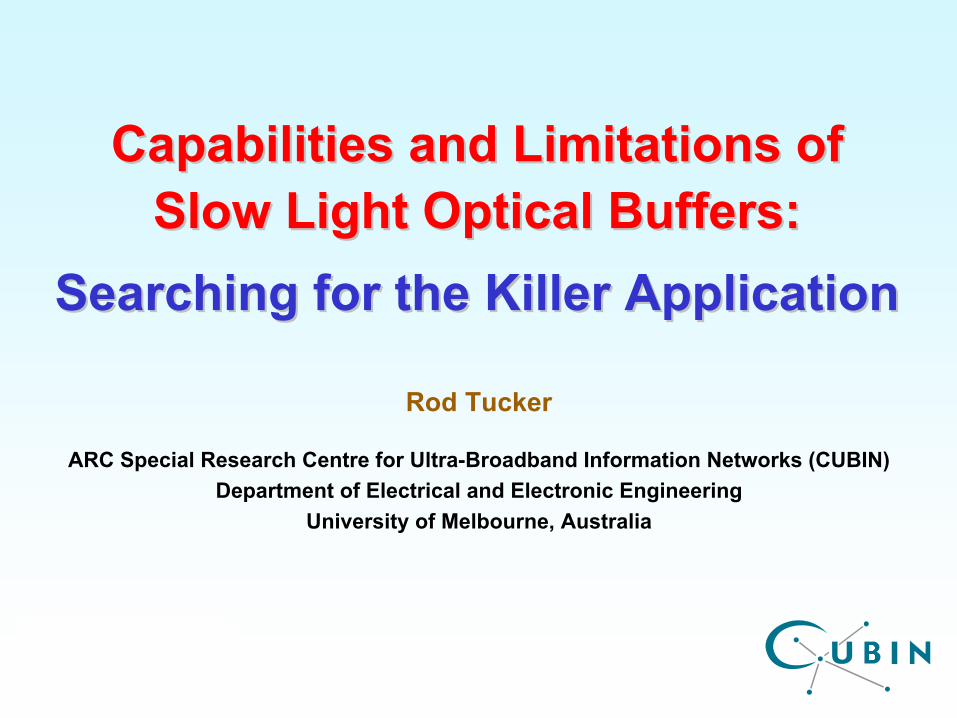
SummarySummary
•
Slow light and optical data-
Group velocity and data bit-size compression
•
Optical delay lines and buffers-
Signal bandwidth and information bandwidth-
FIFO buffers
•
Properties of an ideal slow light medium-
Delay-bandwidth product
•
Requirements of practical optical buffers-
Storage density-
Dispersion-
Attenuation
•
Busting some slow light myths
•
Data storage in high-Q resonators
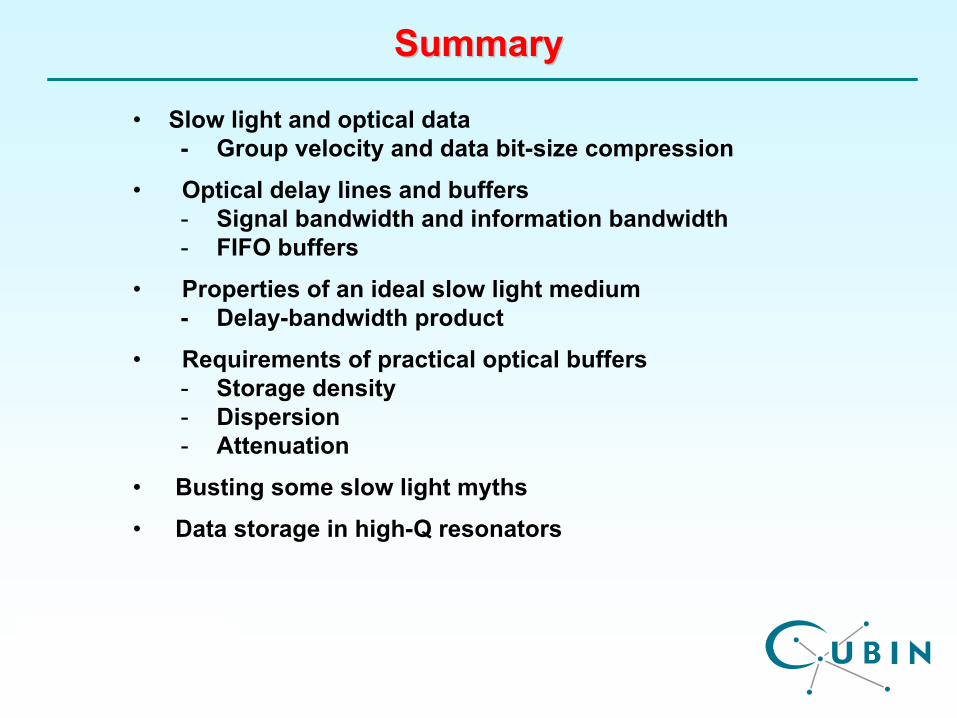
Delay LineInput Output
Group VelocityGroup Velocity
x
gcv dnk n
d
ω
ωω
∂= =
∂ +Group velocity:
Optical frequency
Intrinsic attenuation:1 1
abs g abs
dnnv c d
α ωτ τ ω
⎛ ⎞= +⎜ ⎟⎝ ⎠
Waveguide loss (dB/cm) Absorption time (ns)
0.01 300.1 3
Time to attenuate by e-1
ω
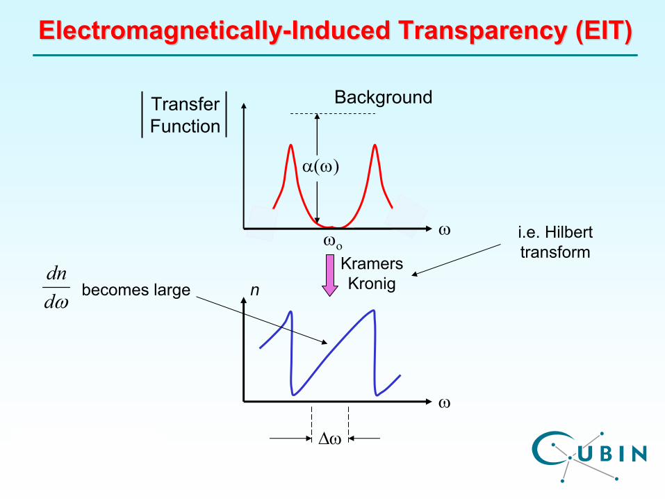
Transfer Function
ωο
α(ω)
ω
n
Δω
Background
Kramers
Kronig
i.e. Hilbert transform
ωddn
becomes large
ElectromagneticallyElectromagnetically--Induced Transparency (EIT)Induced Transparency (EIT)
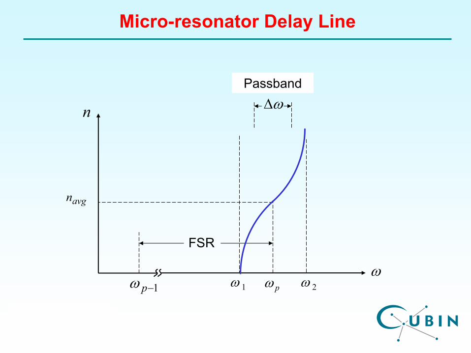
ω
n
FSR
avgn
Passband
pω
ωΔ
1−pω 2ω1ω
Micro-resonator Delay Line
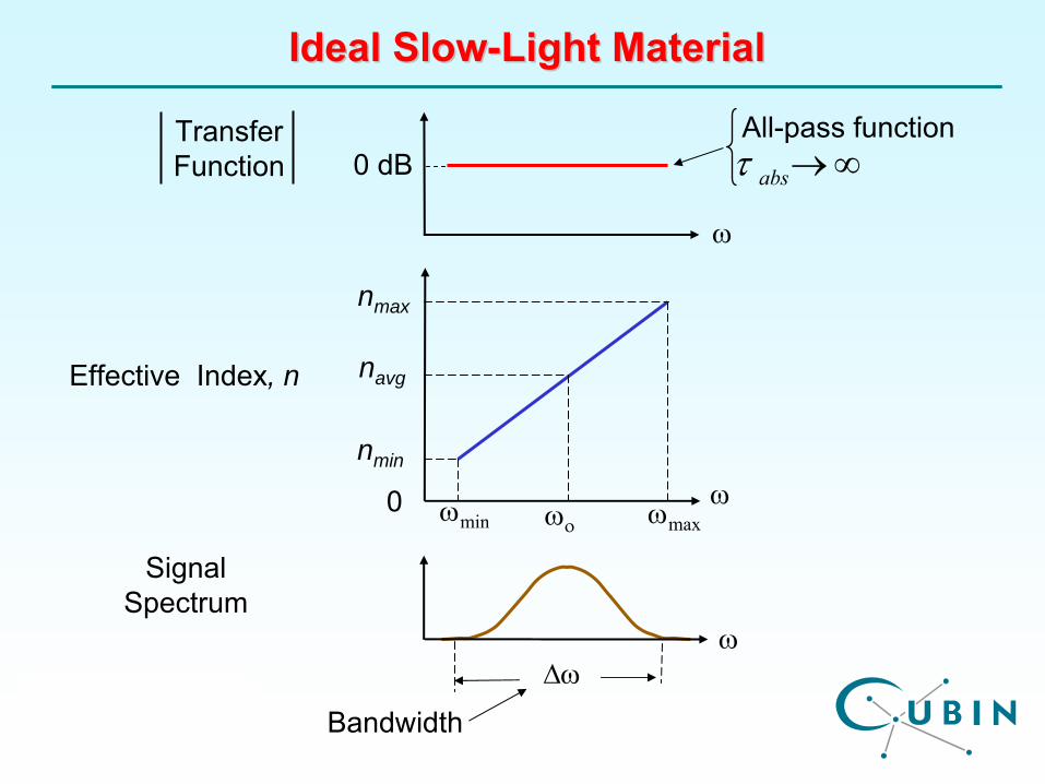
Ideal SlowIdeal Slow--Light MaterialLight Material
Effective Index, n navg
ωωο
ω
Δω
0
nmin
ωmin ωmax
Bandwidth
0 dB
nmax
absτ →∞
ω
Signal Spectrum
Transfer Function
All-pass function
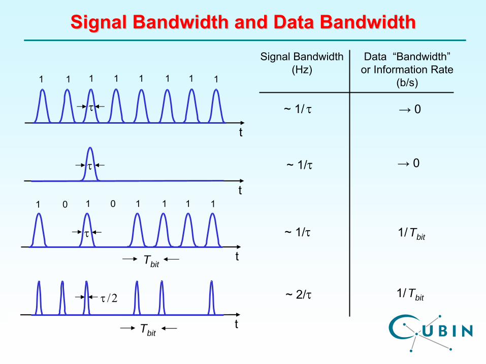
Signal Bandwidth and Data BandwidthSignal Bandwidth and Data BandwidthData “Bandwidth”
or Information Rate
(b/s)
Signal Bandwidth (Hz)
→ 0
t
t
t
t
~ 1/τ 1/Tbit
~ 1/τ
~ 1/
τ
~ 2/τ
τ
τ /2
τ
τ
Tbit
Tbit
1/Tbit
→ 0
1 1 11 1 11 1
1 0 01 1 11 1
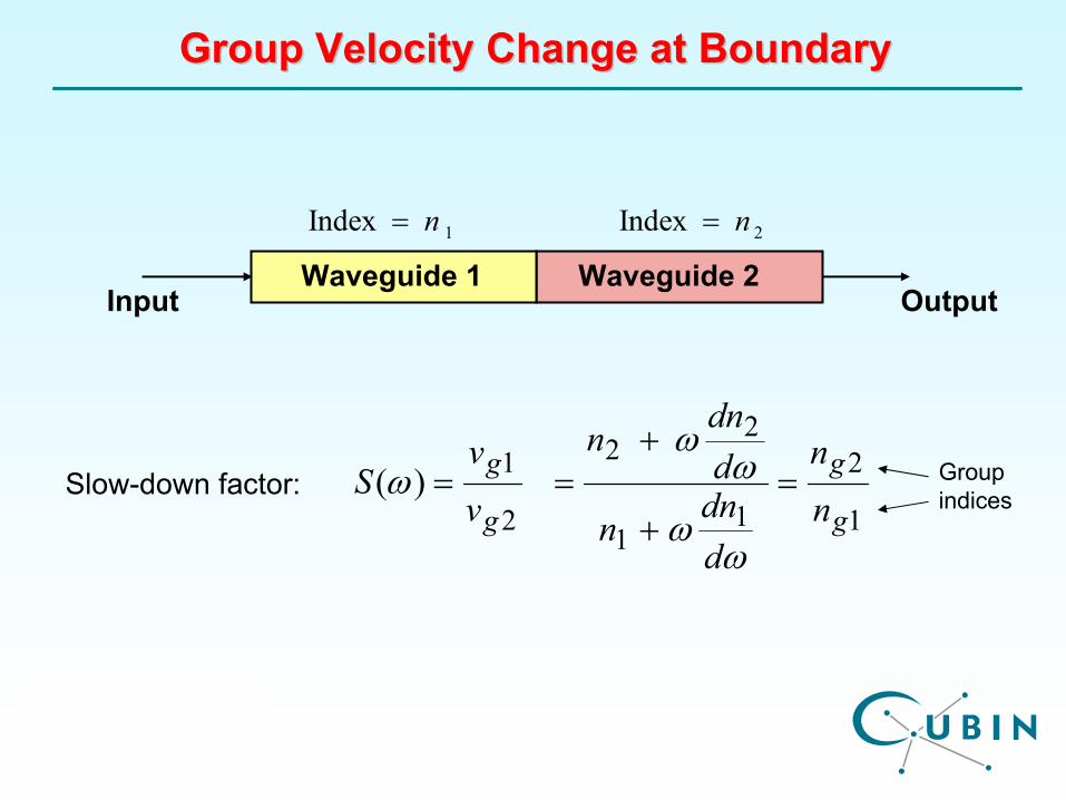
Waveguide 1Input Output
Group Velocity Change at BoundaryGroup Velocity Change at Boundary
1
2
11
22
2
1(g
g
g
g
nn
ddnn
ddn
n
vv
S =+
+==)
ωω
ωω
ω
Waveguide 2
Slow-down factor:
1Index n= 2Index n=
Group indices
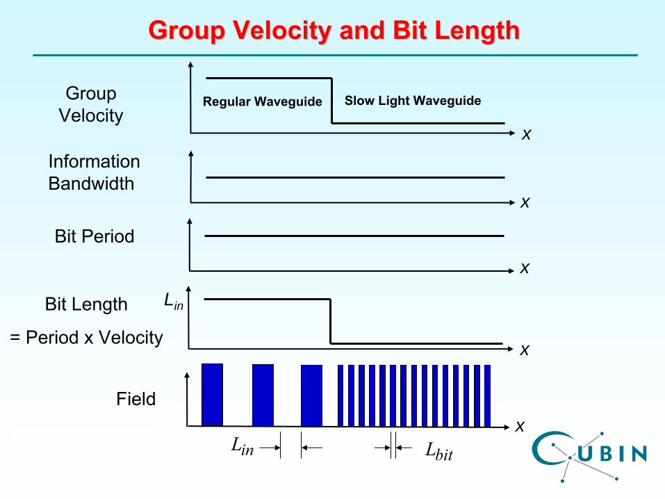
Group Velocity and Bit LengthGroup Velocity and Bit Length
x
Information Bandwidth
Bit Period
LinBit Length
= Period x Velocity x
x
Group Velocity
x
Regular Waveguide Slow Light Waveguide
Fieldx
inL bitL
Reduced Group Velocity Constant Bitrate
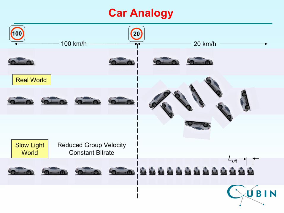
Car Analogy
Slow Light World
Lbit
Real World
100 km/h 20 km/h20100
x
vg
x
Fiel
dvg1
vg2
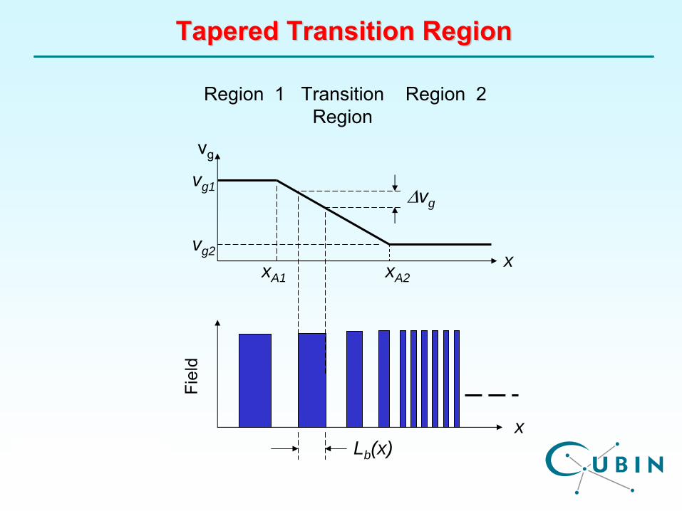
Region 1 Region 2Transition Region
Δvg
xA1 xA2
Lb (x)
Tapered Transition RegionTapered Transition Region
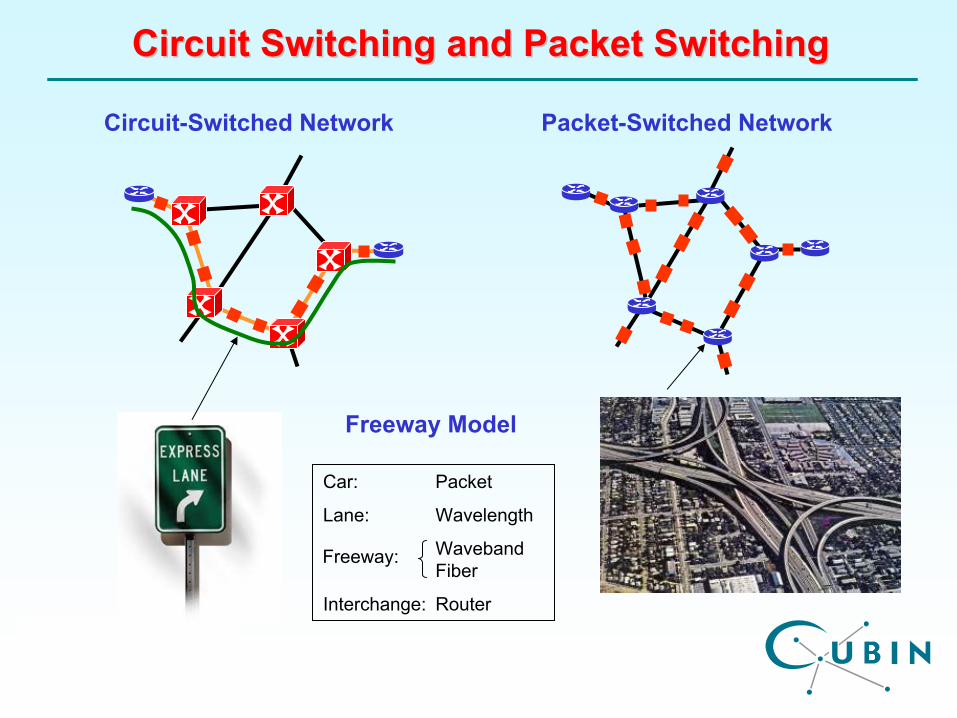
Circuit Switching and Packet SwitchingCircuit Switching and Packet Switching
Circuit-Switched Network Packet-Switched Network
Freeway Model
Car:
Packet
Lane:
Wavelength
Waveband Fiber
Interchange: Router
Freeway:
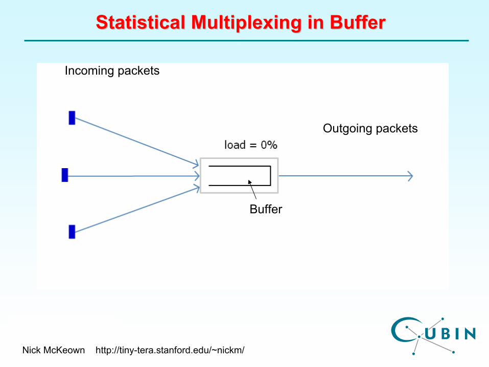
Statistical Multiplexing in BufferStatistical Multiplexing in Buffer
Buffer
Outgoing packets
Incoming packets
Nick McKeown http://tiny-tera.stanford.edu/~nickm/
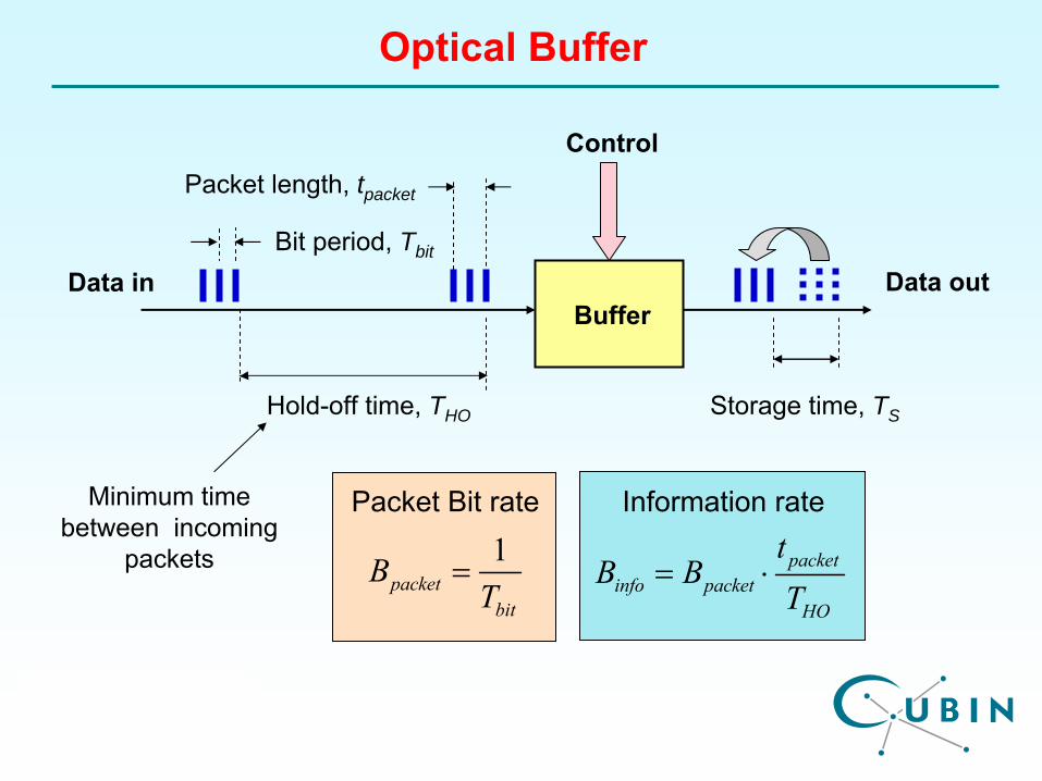
Storage time, TSHold-off time, THO
Packet length, tpacket
Bit period, Tbit
Buffer
Control
Data outData in
Optical Buffer
1packet
bit
BT
=
Packet Bit rate
packetinfo packet
HO
tB B
T= ⋅
Information rateMinimum time between incoming
packets
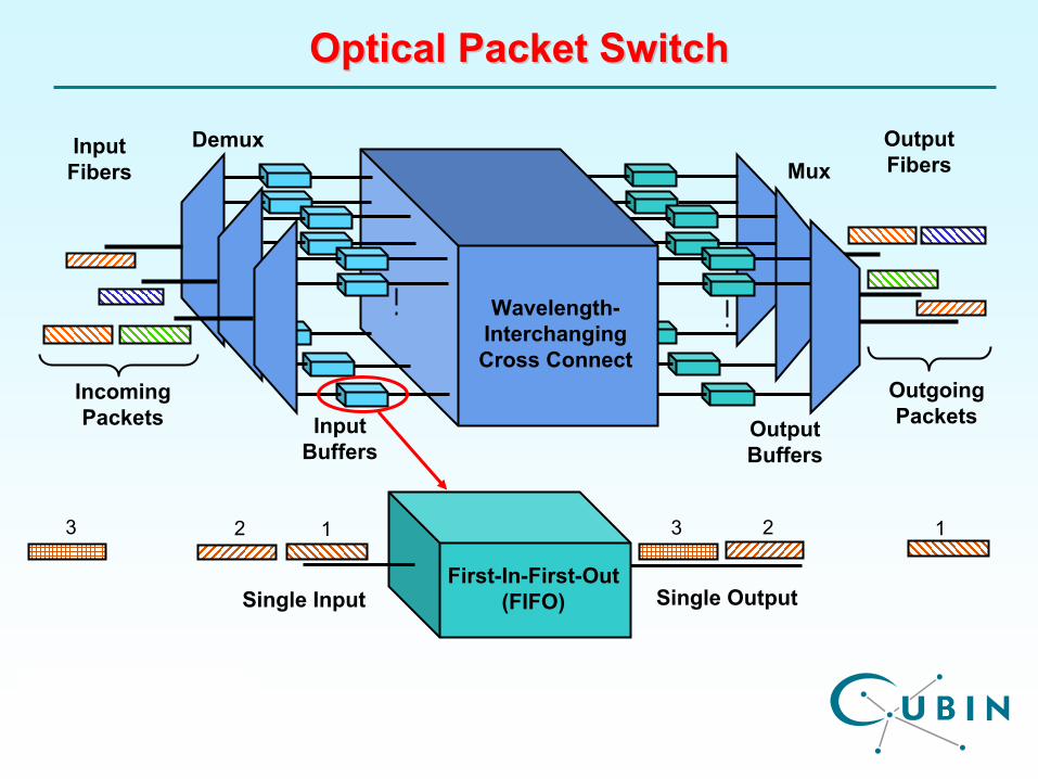
Optical Packet SwitchOptical Packet Switch
First-In-First-Out (FIFO)Single Input Single Output
123 123
Demux
Wavelength-
Interchanging Cross Connect
MuxInput
FibersOutput Fibers
Incoming Packets
Outgoing PacketsOutput
BuffersInput
Buffers
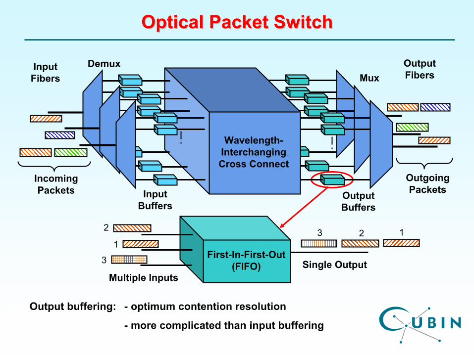
Optical Packet SwitchOptical Packet Switch
First-In-First-Out (FIFO)
Multiple InputsSingle Output
Output Buffers
Input Buffers
Output buffering: -
optimum contention resolution
-
more complicated than input buffering
1
2
3
123
Demux
Wavelength-
Interchanging Cross Connect
MuxInput
FibersOutput Fibers
Incoming Packets
Outgoing Packets
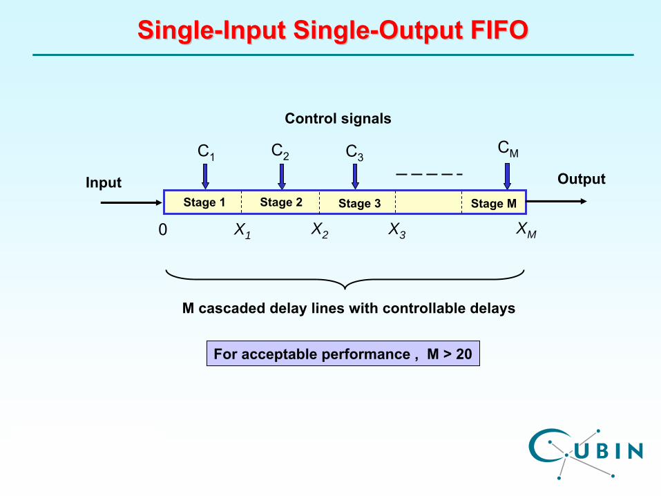
SingleSingle--Input SingleInput Single--Output FIFOOutput FIFO
C1 C3C2CM
M cascaded delay lines with controllable delays
Control signals
Input Output
0 X1 X2 X3
For acceptable performance , M > 20
XM
Stage 1 Stage 3Stage 2 Stage M
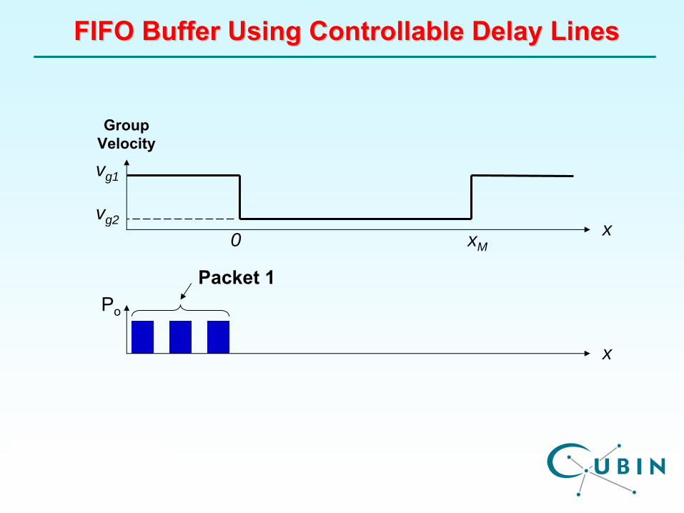
0
vg1
vg2
Po
x
x
xM
FIFO Buffer Using Controllable Delay LinesFIFO Buffer Using Controllable Delay Lines
Packet 1
Group Velocity
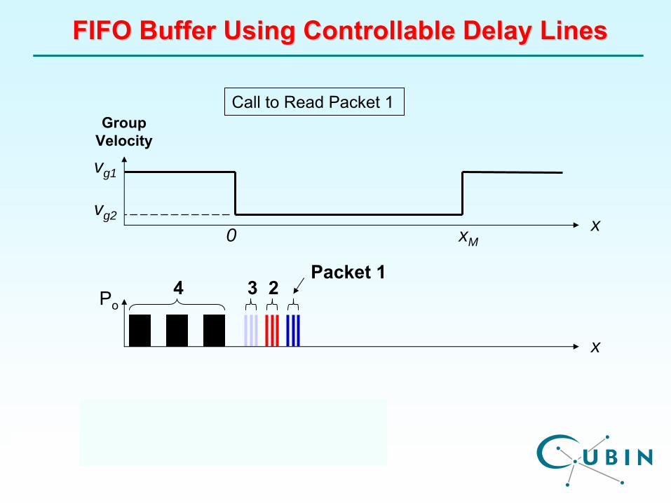
0 xM
vg1
vg2
Po4 3 2
x
x
Call to Read Packet 1
Packet 1
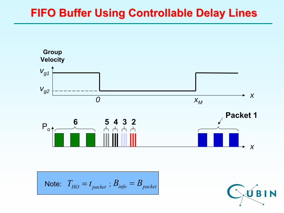
FIFO Buffer Using Controllable Delay LinesFIFO Buffer Using Controllable Delay Lines
Group Velocity
HO packetT t=Note: ; info packetB B=
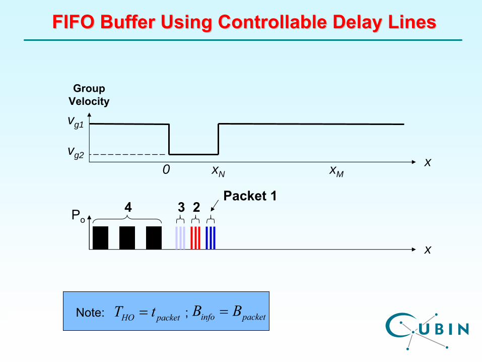
xNx
vg1
vg2
0
Po
x
xM
4 3 2Packet 1
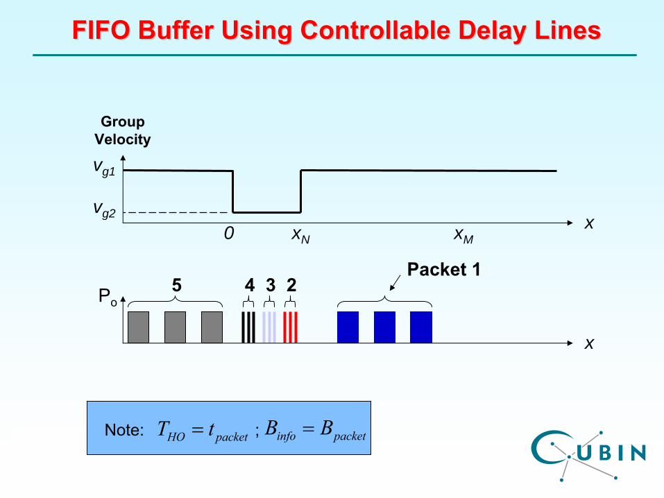
FIFO Buffer Using Controllable Delay LinesFIFO Buffer Using Controllable Delay Lines
Group Velocity
HO packetT t=Note: ; info packetB B=
Po4 3 25
x
vg1
vg2
0
x
xMxN
Packet 1
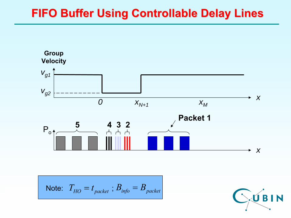
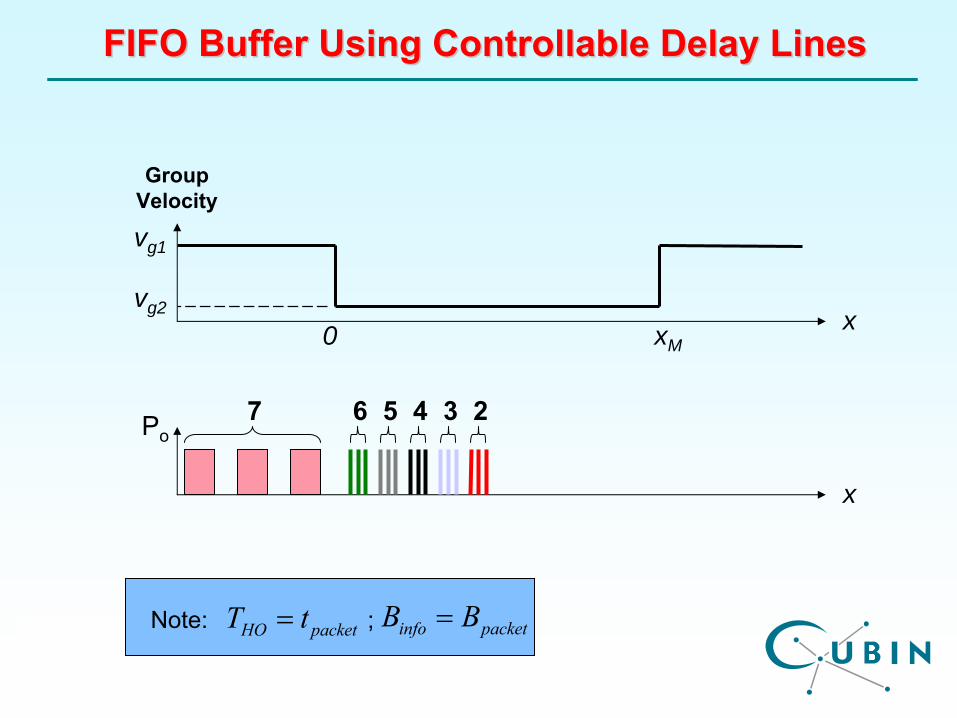
FIFO Buffer Using Controllable Delay LinesFIFO Buffer Using Controllable Delay Lines
Group Velocity
HO packetT t=Note: HO packetT t=Note: ; info packetB B=
Po4 3 25
x
vg1
vg2
0
x
xMxN+1
Packet 1
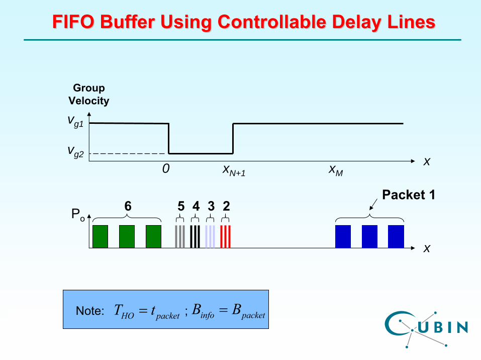
FIFO Buffer Using Controllable Delay LinesFIFO Buffer Using Controllable Delay Lines
Group Velocity
HO packetT t=Note: ; info packetB B=
Po
x
vg1
vg2
0
x
xM
25 4 36
xN+1
Packet 1
FIFO Buffer Using Controllable Delay LinesFIFO Buffer Using Controllable Delay Lines
Group Velocity
HO packetT t=Note: ; info packetB B=
x
Po25 4 36
0
vg1
vg2 xxM
Packet 1
FIFO Buffer Using Controllable Delay LinesFIFO Buffer Using Controllable Delay Lines
Group Velocity
HO packetT t=Note: ; info packetB B=
x
Po36 5 47
0
vg1
vg2 xxM
2
FIFO Buffer Using Controllable Delay LinesFIFO Buffer Using Controllable Delay Lines
Group Velocity
HO packetT t=Note: ; info packetB B=
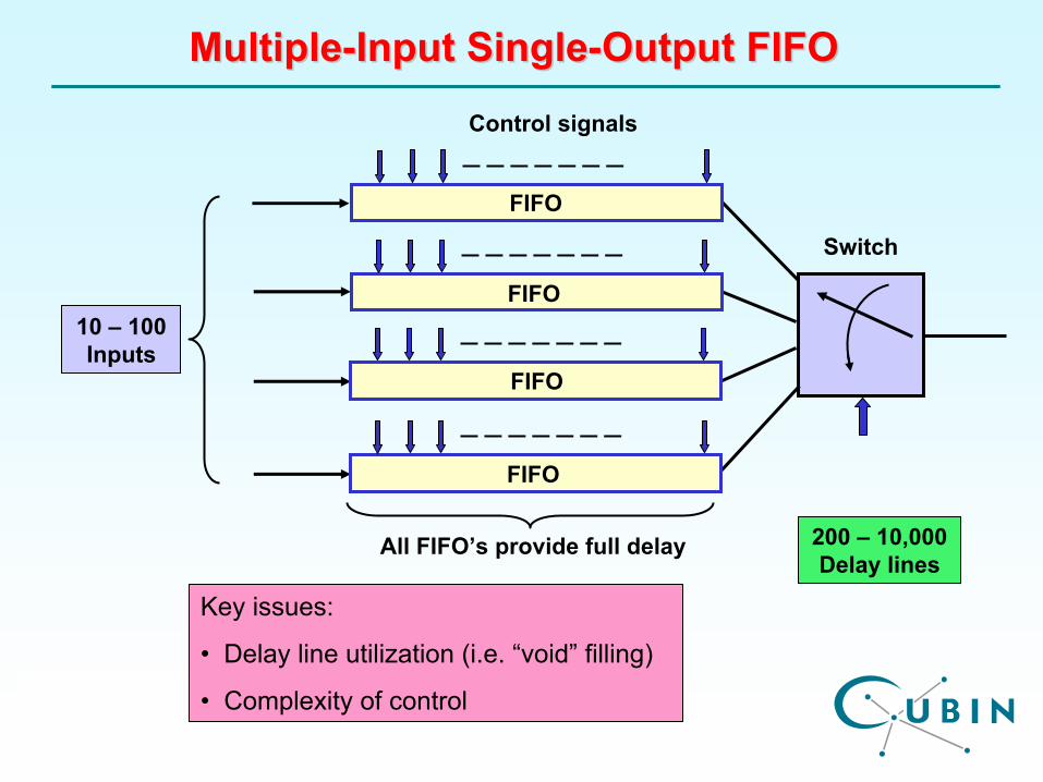
MultipleMultiple--Input SingleInput Single--Output FIFOOutput FIFO
Switch
All FIFO’s
provide full delay
FIFO
FIFO
FIFO
FIFO
Control signals
Key issues:
• Delay line utilization (i.e. “void”
filling)
• Complexity of control
10 –
100 Inputs
200 –
10,000 Delay lines
x
vg
Gro
up V
eloc
ity P
rofil
e
Field
vg1
vg2
Input Region
Slow Light Region
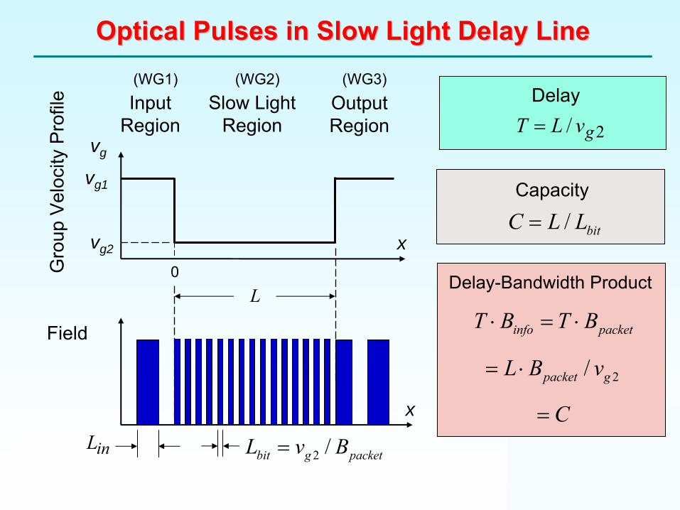
Optical Pulses in Slow Light Delay LineOptical Pulses in Slow Light Delay Line
L
2/ gvLT =Delay
inL2 /bit g packetL v B=
/ bitC L L=Capacity
Output Region
info packetT B T B⋅ = ⋅
Delay-Bandwidth Product0
(WG1) (WG3)(WG2)
2/packet gL B v= ⋅
C=x
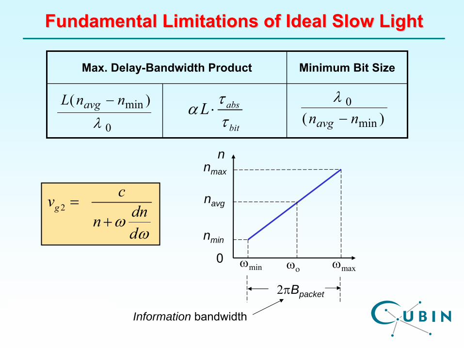
Max. Delay-Bandwidth Product Minimum Bit Size
0
min )(λ
nnL avg −)( min
0nnavg −
λabs
bit
L τατ⋅
Fundamental Limitations of Ideal Slow LightFundamental Limitations of Ideal Slow Light
navg
ωο
2πBpacket
0
nmin
ωmin ωmax
nmax
2gcv dnn
dω
ω
=+
n
Information bandwidth
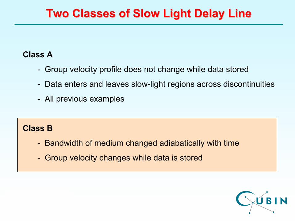
Two Classes of Slow Light Delay LineTwo Classes of Slow Light Delay Line
Class A
- Group velocity profile does not change while data stored
- Data enters and leaves slow-light regions across discontinuities
- All previous examples
Class B
- Bandwidth of medium changed adiabatically with time
- Group velocity changes while data is stored
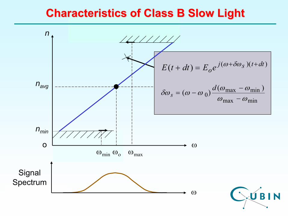
n
navg
ω
nmin
ωmax
))(()( dttsjoeEdttE ++=+ δωω
minmax
minmax0
)()(ωωωωωωδω
−−
−=d
s
ωο
oωmin
ω
Signal Spectrum
Characteristics of Class B Slow LightCharacteristics of Class B Slow Light
x
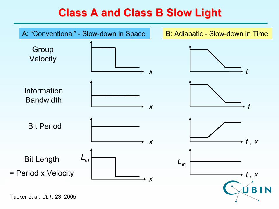
Class A and Class B Slow LightClass A and Class B Slow Light
Bit Period
LinBit Length
= Period x Velocityx
x
Group Velocity
x
Lin
t
t
A: “Conventional”
-
Slow-down in Space B: Adiabatic -
Slow-down in Time
t , x
t , x
Tucker et al., JLT, 23, 2005
Information Bandwidth
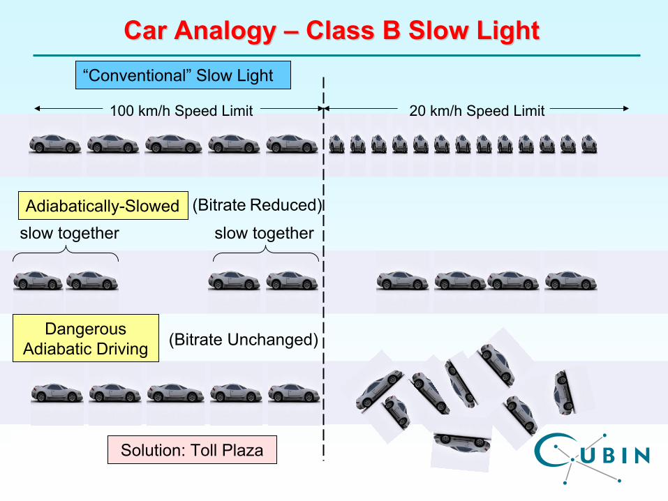
Car Analogy Car Analogy ––
Class B Slow LightClass B Slow Light“Conventional”
Slow Light
Adiabatically-Slowed
Dangerous Adiabatic Driving
20 km/h Speed Limit100 km/h Speed Limit
slow togetherslow together
Solution: Toll Plaza
(Bitrate
Reduced)
(Bitrate Unchanged)
t
vg
x
vg1
vg2
bitL
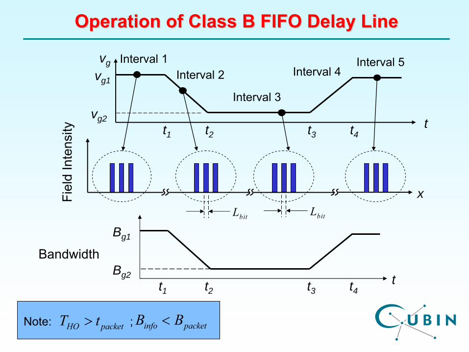
Interval 1Interval 2
Bandwidth
t
Bg1
Bg2
t1 t2 t4t3
t1 t2 t3 t4
Interval 4
Interval 3
Interval 5Fi
eld
Inte
nsity
Operation of Class B FIFO Delay LineOperation of Class B FIFO Delay Line
HO packetT t>Note: ; info packetB B<
bitL
x
vg
vg1
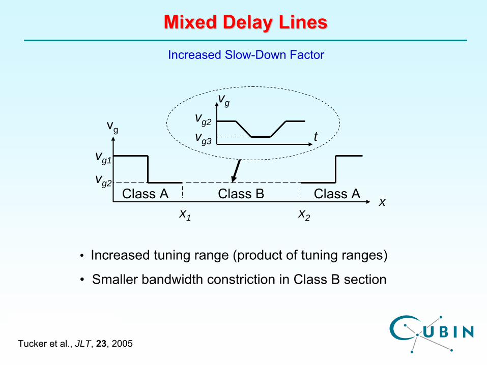
vg2Class A Class B Class A
x1 x2
t
vg
vg2
vg3
Increased Slow-Down Factor
Mixed Delay LinesMixed Delay Lines
• Increased tuning range (product of tuning ranges)
• Smaller bandwidth constriction in Class B section
Tucker et al., JLT, 23, 2005
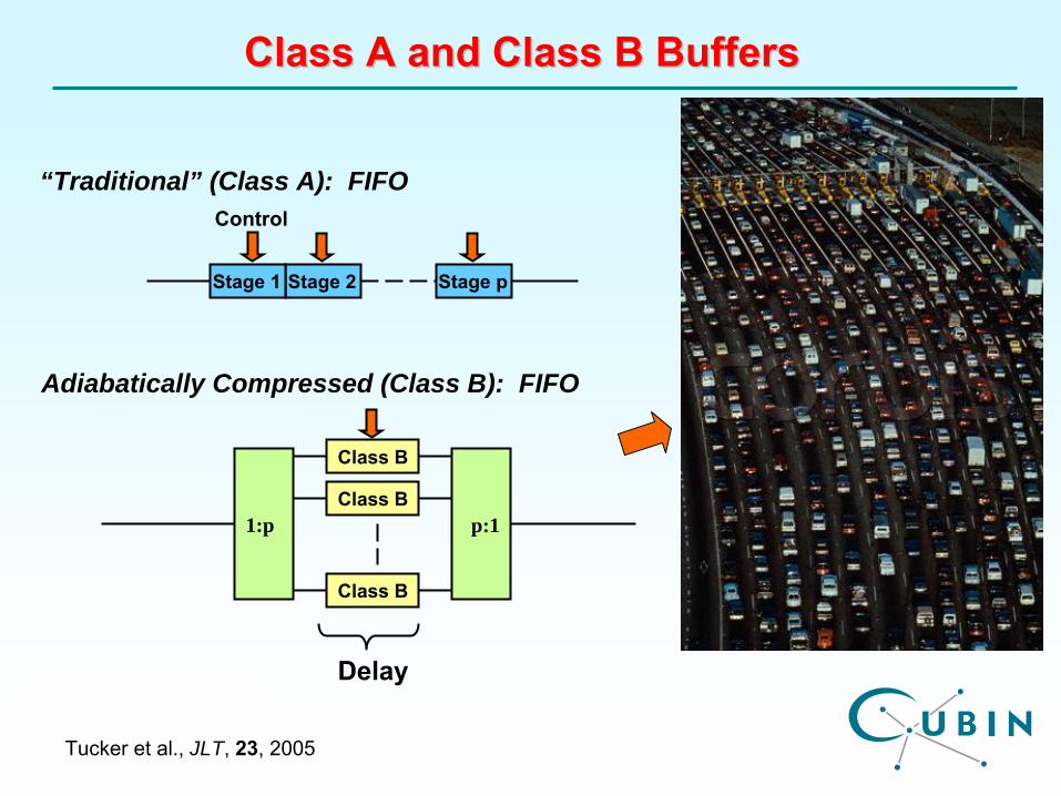
Class A and Class B BuffersClass A and Class B Buffers
1:p p:1
Class B
Stage pStage 2Stage 1
“Traditional” (Class A): FIFO
Adiabatically Compressed (Class B): FIFO
Delay
Tucker et al., JLT, 23, 2005
Class B
Class B
Scaling
SizeEnergy/bit
Cap
acity
Capacity 2
p
Capacity 2
Control
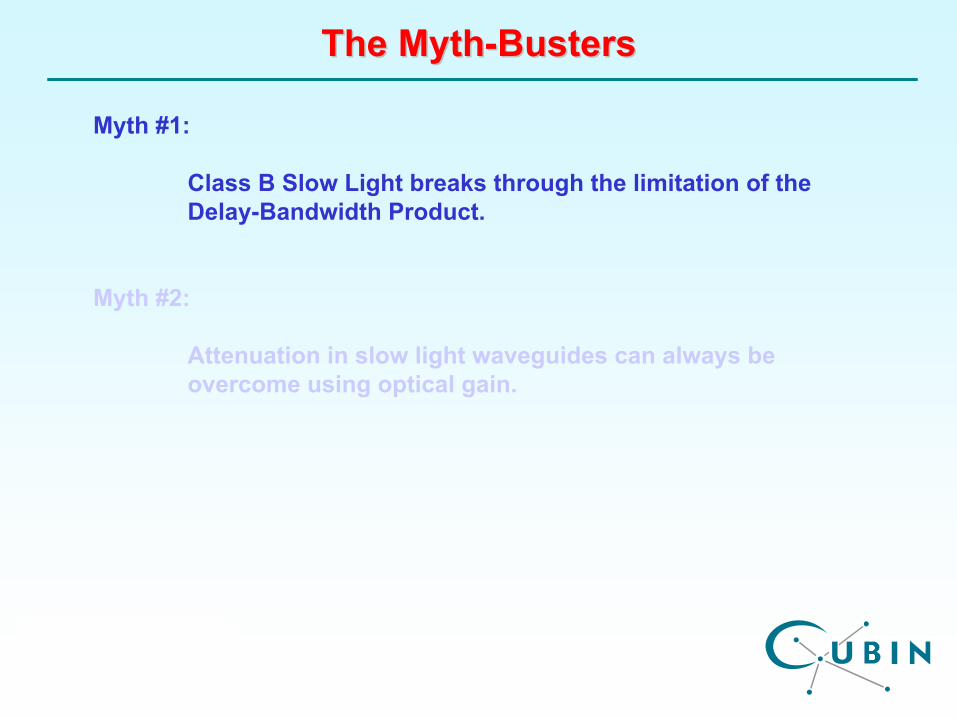
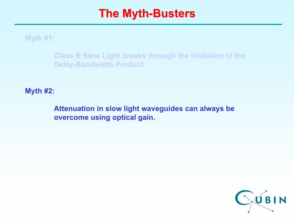
The MythThe Myth--BustersBusters
Myth #1:
Class B Slow Light breaks through the limitation of the Delay-Bandwidth Product.
Myth #2:
Attenuation in slow light waveguides can always be overcome using optical gain.
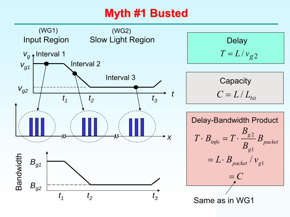
Input Region Slow Light Region
Myth #1 BustedMyth #1 Busted
2/ gvLT =Delay
/ bitC L L=Capacity
2
1
ginfo packet
g
BT B T B
B⋅ = ⋅
Delay-Bandwidth Product
(WG1) (WG2)
1/packet gL B v= ⋅
C=
Same as in WG1
vg
vg1
vg2
Interval 1Interval 2
Ban
dwid
th Bg1
Bg2
t1 t2 t3
t1 t2 t3
Interval 3
t
x
.
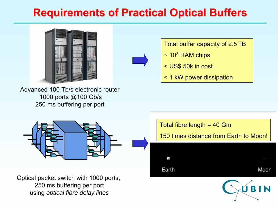
Requirements of Practical Optical BuffersRequirements of Practical Optical Buffers
Advanced 100 Tb/s electronic router 1000 ports @100 Gb/s
250 ms buffering per port
Optical packet switch with 1000 ports, 250 ms buffering per port
using optical fibre delay lines
Total buffer capacity of 2.5
TB
~ 103
RAM chips
< US$ 50k in cost
< 1 kW power dissipation
Total fibre length = 40 Gm
150 times distance from Earth to Moon!
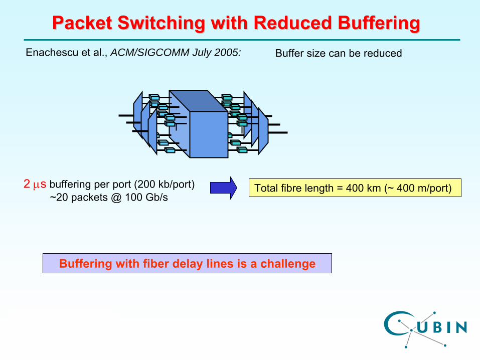
Packet Switching with Reduced BufferingPacket Switching with Reduced BufferingEnachescu
et al., ACM/SIGCOMM July 2005: Buffer size can be reduced
Buffering with fiber delay lines is a challenge
2 μs
buffering per port (200 kb/port) ~20 packets @ 100 Gb/s
Total fibre length = 400 km (~ 400 m/port)
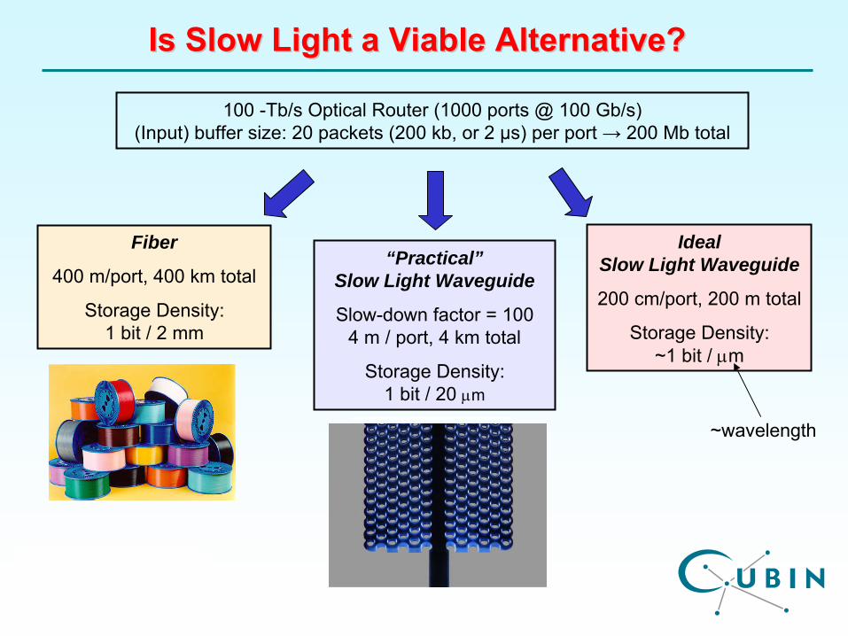
Is Slow Light a Viable Alternative?Is Slow Light a Viable Alternative?
.
100 -Tb/s Optical Router (1000 ports @ 100 Gb/s)(Input) buffer size: 20 packets (200 kb, or 2 μs) per port → 200 Mb total
Fiber
400 m/port, 400 km total
Storage Density: 1 bit / 2 mm
“Practical” Slow Light Waveguide
Slow-down factor = 100 4 m / port, 4 km total
Storage Density: 1 bit / 20 μm
Ideal Slow Light Waveguide
200 cm/port, 200 m total
Storage Density: ~1 bit / μm
~wavelength
λ
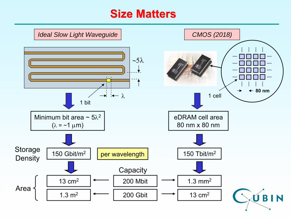
Size MattersSize Matters
Minimum bit area ~ 5λ2
(λ
= ~1 μm)
150 Gbit/m2
∼5λ
1 bit
Ideal Slow Light Waveguide CMOS (2018)
80 nm1 cell
eDRAM
cell area 80 nm x 80 nm
150 Tbit/m2
1.3 mm2
13 cm2
13 cm2 200 Mbit
1.3 m2 200 Gbit
Capacity
Area
Storage Density per wavelength
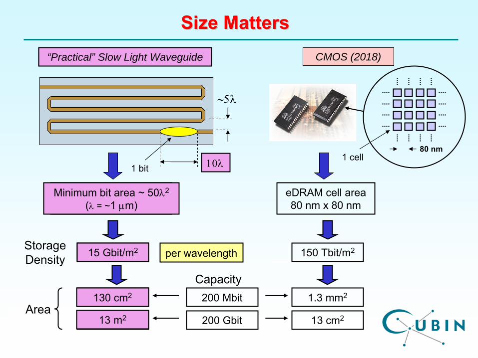
Size MattersSize Matters
Minimum bit area ~ 5λ2
(λ
= ~1 μm)
150 Gbit/m2
∼5λ
1 bit
Ideal Slow Light Waveguide CMOS (2018)
80 nm1 cell
eDRAM
cell area 80 nm x 80 nm
150 Tbit/m2
1.3 mm2
13 cm2
13 cm2 200 Mbit
1.3 m2 200 Gbit
Capacity
Area
Storage Density per wavelength
Minimum bit area ~ 50λ2
(λ
= ~1 μm)
15 Gbit/m2
10λ
“Practical” Slow Light Waveguide
130 cm2
13 m2
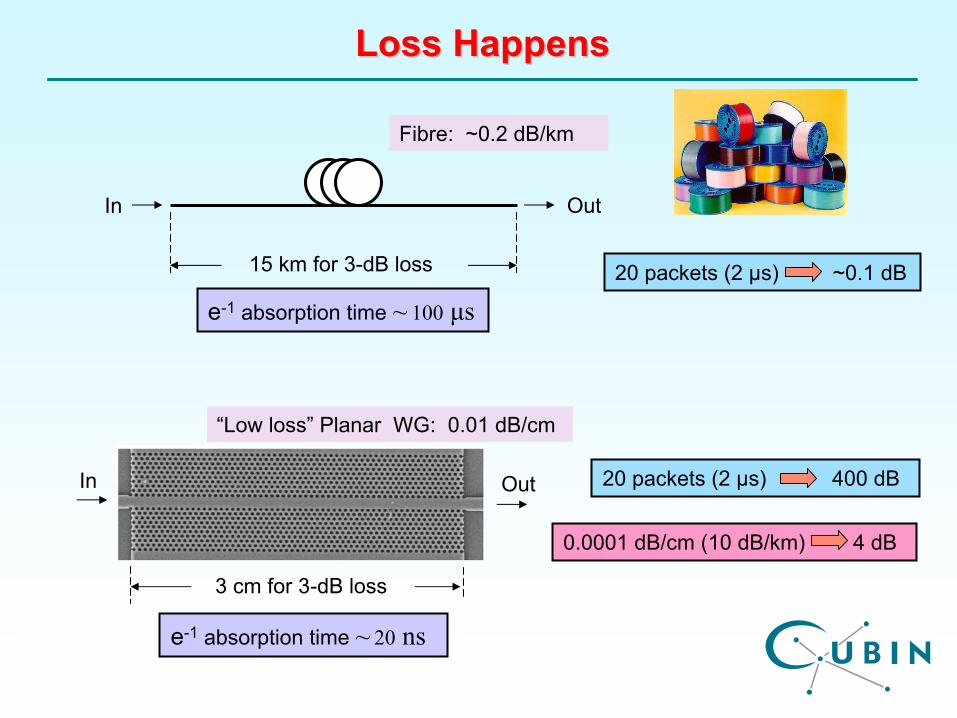
Loss HappensLoss Happens
Fibre: ~0.2 dB/km
In Out
15 km for 3-dB loss
“Low loss”
Planar WG: 0.01 dB/cm
InOut
3 cm for 3-dB loss
20 packets (2 μs) ~0.1 dB
e-1
absorption time ~ 100
μs
In
e-1
absorption time ~ 20
ns
20 packets (2 μs) 400 dB
0.0001 dB/cm (10 dB/km) 4 dB
The MythThe Myth--BustersBusters
Myth #1:
Class B Slow Light breaks through the limitation of the Delay-Bandwidth Product.
Myth #2:
Attenuation in slow light waveguides can always be overcome using optical gain.
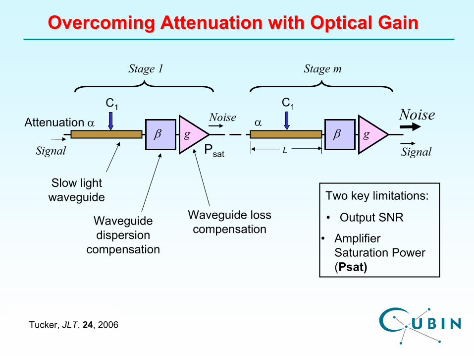
Overcoming Attenuation with Optical GainOvercoming Attenuation with Optical Gain
Signal
Stage 1
g g
Stage m
β β
Slow light waveguide
Waveguide dispersion
compensation
Waveguide loss compensation
SignalPsat
Noise
Two key limitations:
• Output SNR
•
Amplifier Saturation Power (Psat)
Attenuation α α
L
NoiseC1 C1
Tucker, JLT, 24, 2006
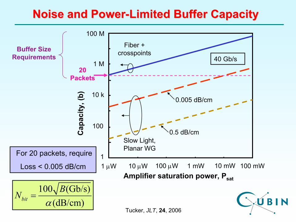
Noise and PowerNoise and Power--Limited Buffer CapacityLimited Buffer Capacity
For 20 packets, require
Loss < 0.005 dB/cm
Tucker, JLT, 24, 2006
Amplifier saturation power, Psat
100 mW10 mW1 mW100 μW10 μW1 μW
Cap
acity
, (b)
1
100
10 k
1 M
100 M
Slow Light, Planar WG
Fiber + crosspoints
0.005 dB/cm
0.5 dB/cm
Buffer Size Requirements
20 Packets
40 Gb/s
100 (Gb/s)(dB/cm)bit
BN
α=
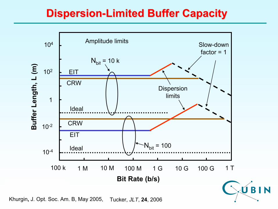
DispersionDispersion--Limited Buffer CapacityLimited Buffer Capacity
Tucker, JLT, 24, 2006
EIT
EIT
Nbit
= 10 k
Nbit
= 100
Slow-down factor = 1
Dispersion limits
Bit Rate (b/s)100 k 1 M 10 M 100 M 1 G 10 G 100 G 1 T
10-4
10-2
1
102
104
Buf
fer L
engt
h, L
(m)
Ideal
Ideal
CRW
CRW
Khurgin, J. Opt. Soc. Am. B, May 2005,
Amplitude limits
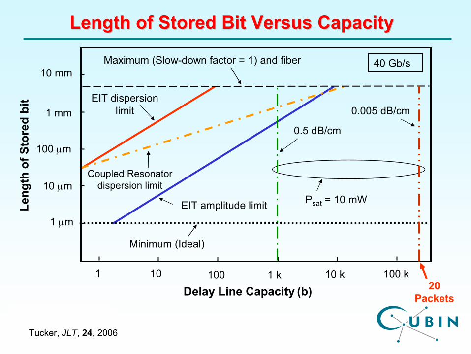
Length of Stored Bit Versus CapacityLength of Stored Bit Versus Capacity
Delay Line Capacity
(b)
Leng
th o
f Sto
red
bit
1 μm
1 10 100 1 k 10 k
10 μm
100 μm
1 mm
10 mm
Minimum (Ideal)
Maximum (Slow-down factor = 1) and fiber
Coupled Resonator dispersion limit
EIT dispersion limit
EIT amplitude limit
40 Gb/s
100 k
0.5 dB/cm
0.005 dB/cm
Psat
= 10 mW
20 Packets
Tucker, JLT, 24, 2006
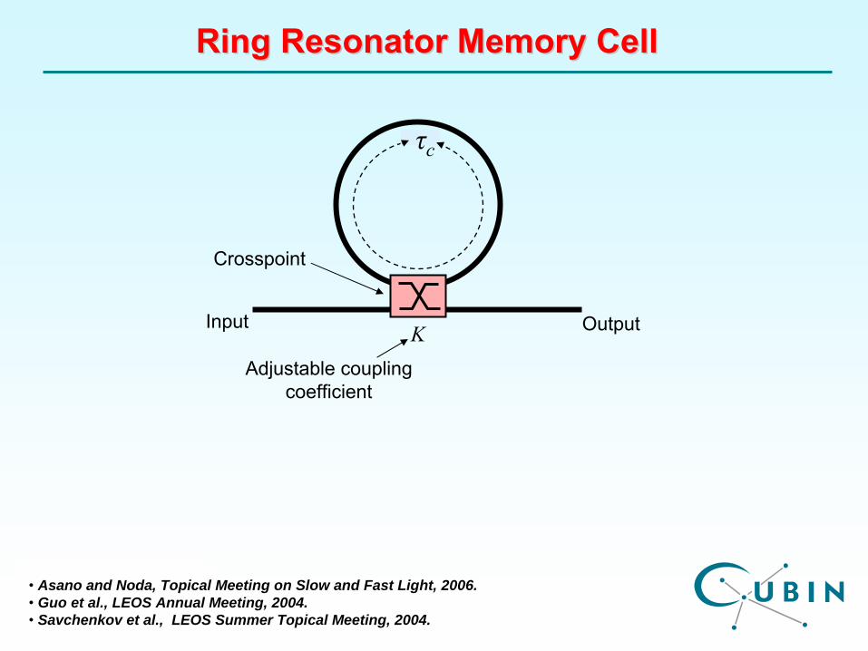
τc
KInput Output
Ring Resonator Memory CellRing Resonator Memory Cell
Adjustable coupling coefficient
Crosspoint
• Asano and Noda, Topical Meeting on Slow and Fast Light, 2006.• Guo et al., LEOS Annual Meeting, 2004.• Savchenkov et al., LEOS Summer Topical Meeting, 2004.
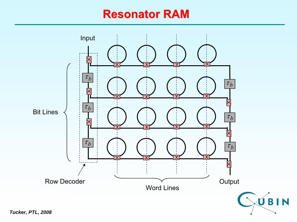
Resonator RAMResonator RAM
bτ
bτ
bτbτ
bτ
bτ
Word Lines
Bit Lines
Row Decoder
Input
Output
Tucker, PTL, 2008
Cou
plin
g C
oeffi
cien
t K
0.0001
0.001
0.01
0.1
1.0
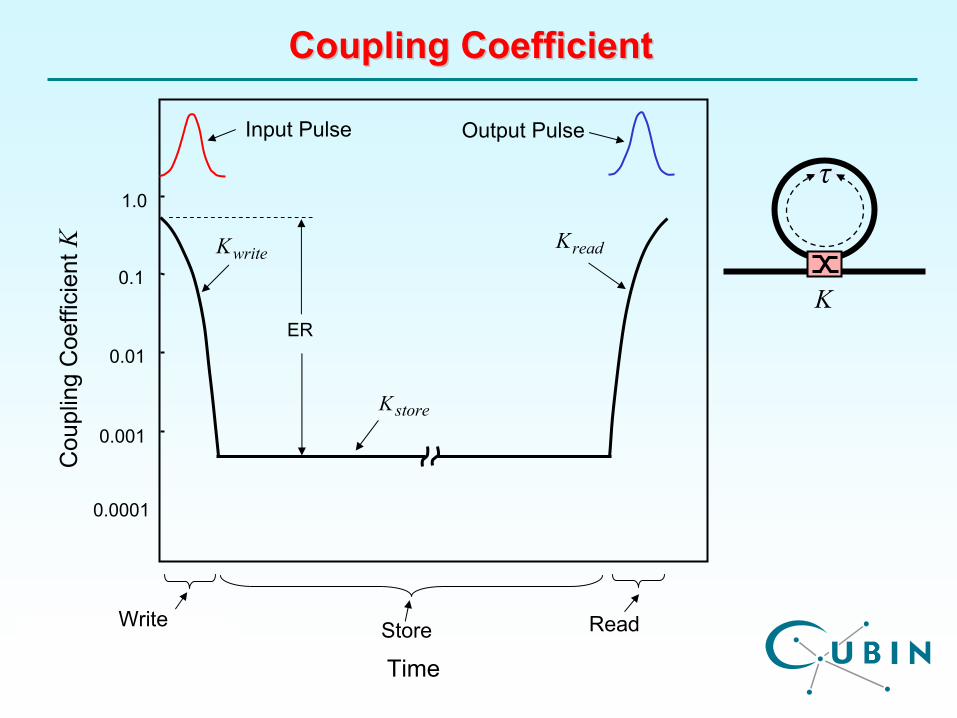
TimeStoreWrite Read
ER
storeK
writeK readK
Coupling CoefficientCoupling Coefficient
Input Pulse Output Pulse
τ
K
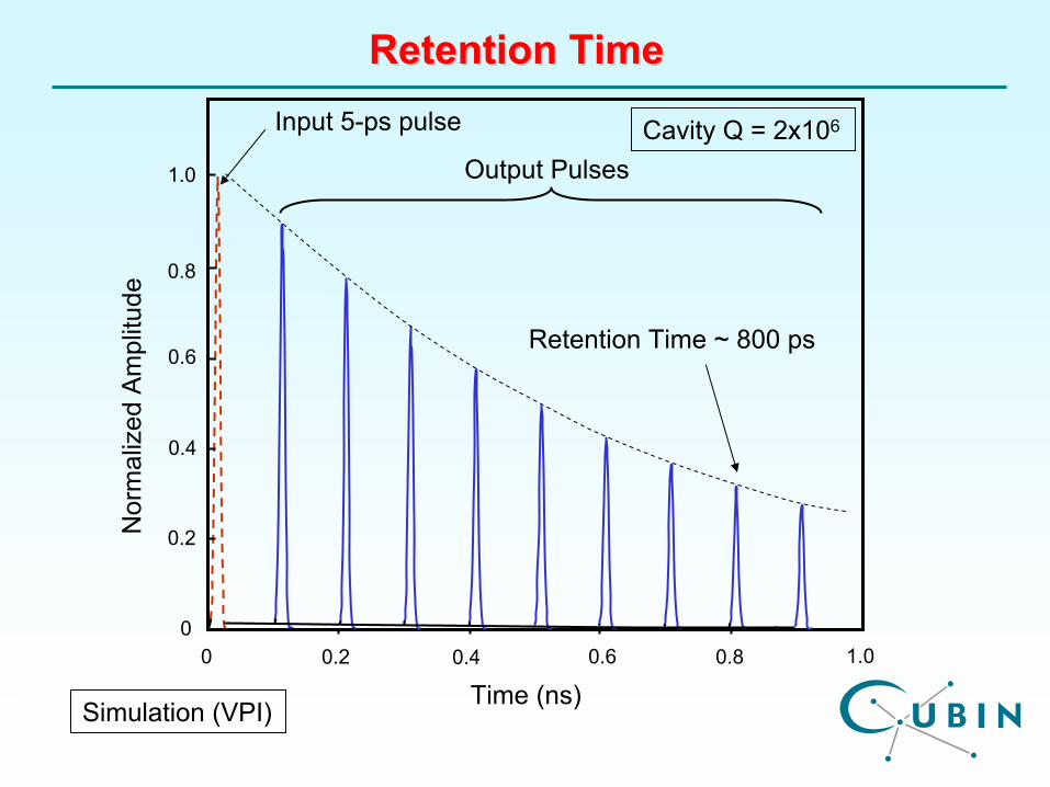
Retention TimeRetention Time
Nor
mal
ized
Am
plitu
de1.0
0.2
0
0.6
0.8
0.4
Time (ns)0 1.00.80.60.40.2
Input 5-ps pulse
Retention Time ~ 800 ps
Cavity Q = 2x10⁶
Output Pulses
Simulation (VPI)
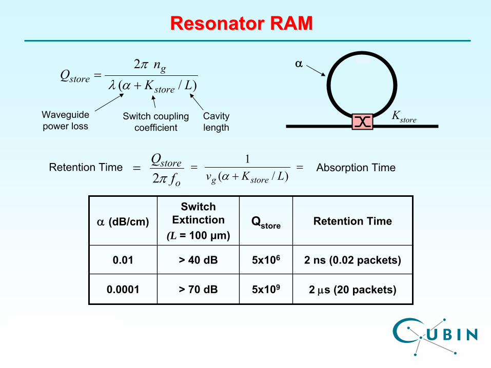
KstoreWaveguide power loss
Switch coupling coefficient
α
(dB/cm)Switch
Extinction(L = 100 μm)
Qstore Retention Time
0.01 > 40 dB 5x10⁶ 2 ns (0.02 packets)
0.0001 > 70 dB 5x10⁹ 2 μs (20 packets)
)/(2
LKn
Qstore
gstore +
=αλ
π
Resonator RAMResonator RAM
o
storef
Qπ2
= =+
=)/(
1LKv storeg α
Retention Time Absorption Time
Cavity length
α
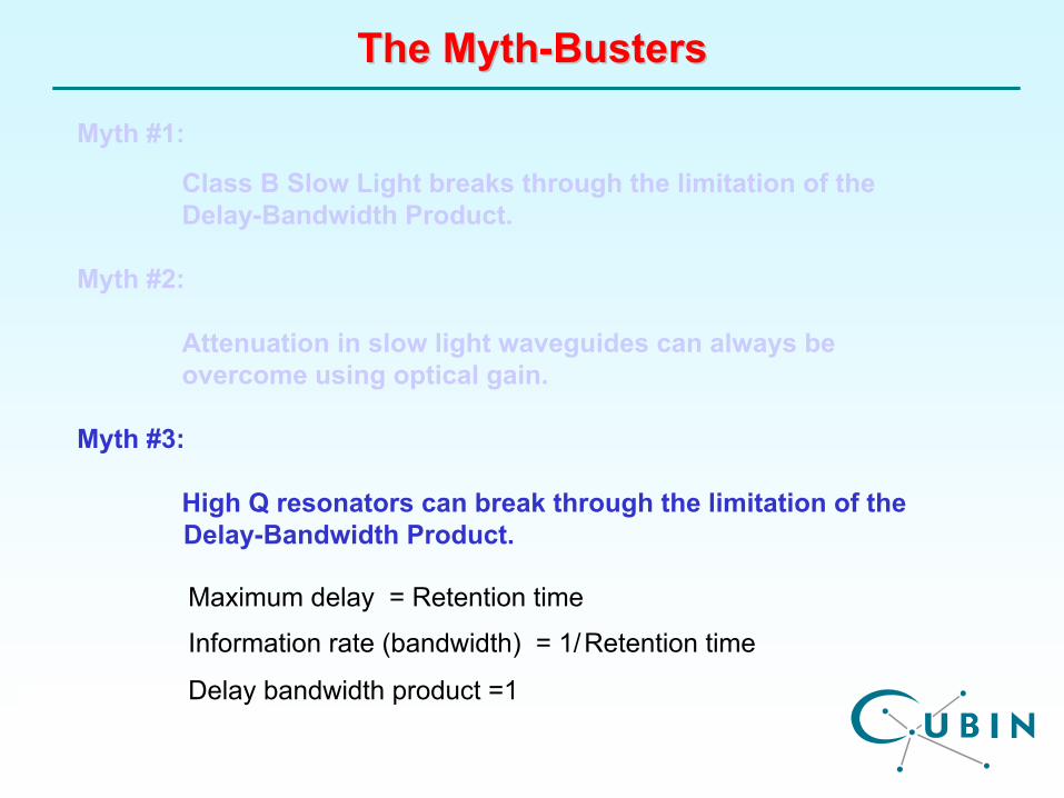
The MythThe Myth--BustersBusters
Myth #1:
Class B Slow Light breaks through the limitation of the Delay-Bandwidth Product.
Myth #2:
Attenuation in slow light waveguides can always be overcome using optical gain.
Myth #3:
High Q resonators can break through the limitation of the Delay-Bandwidth Product.
Maximum delay = Retention time
Information rate (bandwidth) = 1/Retention time
Delay bandwidth product =1
Show stopper
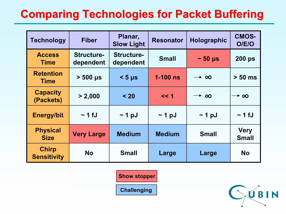
Comparing Technologies for Packet BufferingComparing Technologies for Packet Buffering
Challenging
Technology Fiber Planar, Slow Light Resonator Holographic CMOS-
O/E/O
Access Time
Structure-
dependent
Structure-
dependent Small ~ 50 μs 200 ps
Retention Time > 500 μs < 5 μs 1-100 ns ∞ > 50 ms
Capacity (Packets) > 2,000 < 20 << 1 ∞ ∞Energy/bit ~ 1 fJ ~ 1 pJ ~ 1 pJ ~ 1 pJ ~ 1 fJ
Physical Size Very Large Medium Medium Small Very
Small
Chirp Sensitivity No Small Large Large No
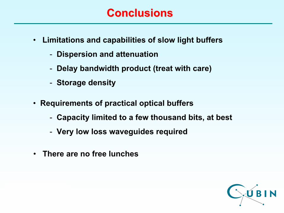
• Limitations and capabilities of slow light buffers
- Dispersion and attenuation
- Delay bandwidth product (treat with care)
- Storage density
• Requirements of practical optical buffers
- Capacity limited to a few thousand bits, at best
- Very low loss waveguides required
ConclusionsConclusions
• There are no free lunches


![[Pgday.Seoul 2017] 3. PostgreSQL WAL Buffers, Clog Buffers Deep Dive - 이근오](https://img.pdfslide.net/doc/110x75/5a65da547f8b9aaf638b5143/pgdayseoul-2017-3-postgresql-wal-buffers-clog-buffers-deep-dive-.jpg)