Embed Size (px)
Citation preview

5-TONE Z V E I E NCO D E R A N A L Y S E R
BRIAN GEORGE WILSON
Thesis submitted in part fulfilment of the requirements
for the Master's Diploma in Technology in the School of
Electrical Engineering at the Cape Technikon.
CAPE TOWN
JANUARY 1993
i

DECLARATION
I declare that the contents of this thesis represents my
own work and the opinions contained herein are my own and
not necessarily those of the Technikon. This thesis has
not been submitted before for any examination at this or
any other institute.
BRlAN GEORGE WILSON
(Name of candidate)
ii
(Signature of candidate)

DEDICATION
This thesis is dedicated to the memory of my dear parents
the late Leonard Raymond Wilson and Dorothy Antoinette
Wilson (nee Vollenhoven) who throughout their lives
provided me with constant support and encouragement in
obtaining a high level of education. It is also dedicated
to my dear wife Lurinda and son Dylan for their patient,
understanding
enjoy.
and supportive manner which I continue to
iii

ACKNOWLEDGEMENT
I would like to thank Mr M.J. van Rensburg, Assistant City
Electrical Engineer, Test and Metering Branch, Cape Town
City Council and Mr Z. Bawolski from the Computer Section
for making this project possible.
iv

SUMMARY
This thesis describes the development of a 5-Tone Zentral
Verband Electrotechische Industrie eZVEI) Encoder
Analyser. The 5-Tone ZVEI Encoder Analyser is used by the
Radio Section of the Test and Metering Branch, which falls
under the Electricity Department of the Cape Town City
Council.
It assists the Quality Assurance Technician in determining
whether the 5 tone ZVEI encoder, of the radio under test,
is operating within the manufacturers specifications.
Various manufacturers of radio equipment tender for the
supply of mobile radios fitted with ZVEI tone
The Radio Section are now capable of testing
encoders.
all the
various radios and comparing the analysed ZVEI
specifications of each manufacturer's radio. The results
can be used to assist management in deciding which radio
would be the most suitable for purchasing.
The development of the 5-Tone ZVEI Encoder Analyser
involved the design and development of hardware and
software. It was designed to be housed in a compact
enclosure and to interface to a Motorola Communications
System Analyser Model R-2001C. The RF output, from the
radio under test, connects to the RF input of the
Communications System Analyser. The demodulated output of
the Communications System Analyser connects to the input
of the 5-Tone ZVEI Encoder Analyser.
v

The softwa~e was designed using PLM-51 high level language
to p~ovide ~eal-time analysis of va~ious selective-calls
(selcalls) ~eceived f~om the demodulated output of the
Communications System Analyser. Once all 5 tones of the
ZVEI selcall have been analysed the software background
task is flagged and the analysed results a~e displayed as
various MODES of display on a 16 cha~acte~ by 4 line dot
matrix display.
The following parameters of the ZVEI selcall a~e analysed:
i) Frequency Digits.
ii) Frequency fo~ each of the 5 tones.
iii) Tone Duration for each of the 5 tones.
iv) Frequency Error for the 5 tones.
v) Tone Duration Er~or for the 5 tones.
The design and development of the 5-Tone ZVEI Encode~
Analyser was conducted at the Computer Section of the
Electricity Depa~tment, Cape Town City Council.
vi

OPSOMMING
Hierdie skripsie beskryf die ontwerp en ontwikkeling van
n 5-Sein Zentral Verband Electrotechische Industrie
(ZVEI) Enkodeerder Ontleedtoestel. Die Toets en Meet
Afdeling van die Elektrisiteits Afdeling van die
Kaapstadse Stadsraad het n 5-Sein ZVEI Enkodeerder
Ontleedtoestel benodig vir gebruik in hul Radio Afdeling.
Die Kwalititeitsversekeringstegnici moet die toestel
gebruik om te verseker dat die 5 Sein ZVEI enkodeerders,
van die radios wat getoets word, aan die vervaardiger se
spesifikasies voldoen.
Verskeie radio vervaardigers doen aansoek om mobiele
radios, toegerus met ZVEI sein enkodeerders, aan die
Kaapstadse Stadsraad te verskaf. Die Radio Afdeling is nou
in staat om die verskillende radio ZVEI spesifikasies te
analiseer en te vergelyk met die van verskillende
vervaardigers. Die ontledings word op bestuursvlak gebruik
om die geskikte radio te keur, wat aangekoop moet word.
Die ontwikkeling van die 5-Sein ZVEI Enkodeerder Ontleed
toestel het die ontwerp en ontwikkeling van apparatuur
sowel as programmatuur behels. Die apparatuur is ontwerp
om in n kompakte verpakking te pas, en dien as koppelvlak
na die " Motorola Communications System Analyser
R-2~~1C.
vii
., Model

Die toets-radio se RF uittree-poort word gekoppel aan die
" Communications System Analyser .. se RF toevoer-poort.
Die ., Communications System Analyser "se gedemoduleerde
uittree-poort dien as toevoer vir die 5-Sein ZVEI
Enkodeerder Ontleed-toestel.
Die programmatuur is met behulp van die PLM-51 hoe vlak
taal geskryf vir intydse ontleding van verskillende
selektiewe oproepe ontvang, vanaf die "Communications
System Analyser se gedemoduleerde uittree-poort. Na
die ontleding van al 5 seine van die ZVEI oproep word die
stadium van program, wat op die agtergrond loop, gemerk en
gestaak. Die ontlede resultate word vertoon as
verskillende MODUSSE op
matriks vertoonkonsole.
'n 16 karakter by 4 lyn punt-
Die volgende parameters van die ZVEI selektiewe oproep
word ontleed:
i) Frekwensie Syfers.
ii) Frekwensie van afsonderlike 5 seine.
iii) Sein Lengte van afsonderlike 5 seine.
iv) Fout in Frekwensie van die 5 seine.
v) Fout in Sein Lengte van die 5 seine.
Die 5-Sein ZVEI Enkodeerder Ontleed-toestel is ont.... ikkel
en ont....erp in die Rekenaar Afdeling van die Elektrisiteits
Afdeling van die Kaapstadse Stadsraad.
viii
OBJECTIVES
The objectives of this ~esea~ch was to accomplish the
following:
il To develop a 5-Tone ZVEI Encode~ Analyse~.
ii) To interface the 5-Tone ZVEI Encode~ Analyse~ to an
existing Communications System Analyse~.
iiil To analyse a 5-tone ZVEI encoded signal as ~egards:
* The decoding of the encoded 5-Tone ZVEI Signal.
* The F~equency fo~ each of the five tones.
* The F~equency E~ro~ fo~ each of the five tones.
* The Tone Du~ation fo~ each of the five tones.
* The Tone Du~ation E~~o~ fo~ each of the five
tones.
ivl To apply the PLM-51 Compile~ as a development tool.
vl To decide on which Mic~op~ocesso~ would be the most
suitable.
ix

CONTENTS
DESCRIPTION PAGE
ACKNOWLEDGEMENT
DECLARATION
DEDICATION . iii
.iv
. ii
.i
.. . . . . . .. . . . . . . . . . . . . . . . .. . . . . . .. . . . .. . . .. .. . . . . . . . . . .. . . . . . . . . . . . . . . ... . ... .. . . . . ..PAGETITLE
SUMMARY: ENGL I SH ••••••••.••••.•••••••••••••.••••••••• v
. . . . . . . .... . . . . . . .... . . . . .. . . .. . . . .. . .. . . .AFRIKAANS
OBJECTIVES
.vii
.ix
LIST OF DIAGRAMS ..... . . . . . . . . . . . . .... .... ... . ... . . ..xiv
LIST OF TABLES ••••••••••••••••••••••.•••••••.••.••••. xv
CHAPTER 1 I N T ROD U C T ION
1.1 General •••••••••.••••••••••••.••.•• 1-1
1.2
1.2.1
1.2.2
Discussion of Signalling Systems ••• 1-2
Selective-Calling Systems •••••••••• 1-2
The ZVEI Choice •••••••••••••.•••••• 1-4
1.3 Motivation •.••.••••••••••••.••••••• 1-5
1.4
1.4.1
1.4.2
1.4.3
1.4.4
1.4.5
Design Approach •••••••.••••••.••.•• 1-5
Choice of Microprocessor ••..••••.•• 1-5
Peripheral Hardware Selection .•••.• 1-6
Need for Emulation •.••.••..•••••••• 1-6
Emulator ••••.•.••.•••.•••.••••••••• 1-7
5-Tone ZVEI Encoder Analyser •.••••• 1-7
x

CHAPTER 2 5-TONE ZVEI ENCODER ANALYSER PAGE
2.1
2.1.1
2.1.2
2.1.3
2.1.4
2.2
2.2.1
2.2.2
2.3
2.3.1
2.3.2
2.3.2.1
2.3.2.2
2.4
2.4.1
2.4.2
2.4.2.1
2.4.2.2
2.4.2.3
2.4.2.4
2.5
2.5.1
2.6
Initial Concepts .•••••••••.••••••••2-1
The ZVEI Standard Frequencies •••••• 2-1
Preliminary Hardware andSoftware Research •••••••••••••••••• 2-2
Initial Design Philosophy ••••••••• 2-12
Final Design Technique ••••.••••••• 2-14
System Integration ••••••••••.••••• 2-16
Interface to CommunicationsSystem Analyser ••••••••••••••••••• 2-16
Communications SystemAnalyser Settings ••••••••••••••••• 2-18
Theory of Operation ••••••••.•••••• 2-19
Hardware •....•.................... 2-19
Sof tware 2-23
Keypad 2-26
Display 2-27
Operating Instructions •••••••••••• 2-27
Precautions 2-27
5-Tone ZVEI Encoder Analyser •••••• 2-28
Powering Up ••••••••.•.••••..•••••• 2-28
Keypad Functions •••••••••••••••••• 2-28
Display Format •.•••.•••••••••••••• 2-28
Display MODE Operation •••••••••••• 2-29
Maintenance ••••••••••••••••••••••• 2-32
Cal ibration ••••••••••••••••••••••• 2-32
5-Tone ZVEl Encoder AnalyserSpecifications .....•.....•••••.••. 2-33
xi
CHAPTER 3 RES U L T S PAGE
3.1
3.1.1
3.1.2
3.2
CHAPTER 4
CHAPTER 5
APPENDIX A
APPENDIX B
APPENDIX C
APPENDIX D
APPENDIX E
APPENDIX F
APPENDIX G
APPENDIX H
APPENDIX I
Functional Tests Using HPMultifunction Synthesizer ••••.••••• 3-1
Table of Test Results •••••••••••••• 3-1
Interpretation of TestResu 1 ts .••.....•...•...•.•••..•••..3-2
Mobile Radio ZVEI TestResul ts •••.•••••••••••••••••••••••• 3-3
Improvements on the 5-ToneZVEI Encoder Analyser •••••••••••••• 4-1
CON C L U S ION •••••••••••••••• 5-1
BIBLIOGRAPHY / LIST OF REFERENCES •• 6-1
A P PEN D I X E S
5-Tone ZVEI Encoder AnalyserCircuit Diagram •...•.•..•...••..•.. 7-1
5-Tone ZVEI Encoder AnalyserSoftware Description ••••••••••••••• 8-1
5-Tone ZVEI Encoder AnalyserFlow Charts •••••••••••••••••••••••• 9-1
5-Tone ZVEI Encoder AnalyserSoftware Listing •••••••••••••••••• 1~-1
Simulated data change signalFlow Charts •••••.•••••••.••••••••. 11-1
Simulated data change signalSoftware Listing ••••.••.•••••.•••. 12-1
Simulated data change signalrepresentation •••••••••••••••.•••• 13-1
MODE ~ to MODE 8 DisplayFormat •...•...•..........••.....•. 14-1
Waveforms of Tone DigitFrequencies •••••••••.••••••••••••• 15-1
xii

ANN E X U RES PAGE
ANNEXURE 1
ANNEXURE 2
Data Sheets on Selective-CallTone Encoders / Decoders .••.•••••• 16-1
5-Tone ZVEI Encoder AnalyserDisplay Documentation ••••••••.•••• 17-1
xiii

LIST OF DIAGRAMS
DESCRIPTION
PAGE
Figure 2.1
Figure 2.2
Figure 2.3
Figure 2.4
Figure 2-5
Figure 2.6
Figure 2.7
Waveform showing all five tones of theencoded 5-Tone ZVEI selcall ••••••••.•••• 2-6
Frequency Change between two of thetones shown in Figure 2.1 ••••••••••••••• 2-7
Data Change Signals output by theFX202QZK •••••••••••••••••••••••••••••••• 2-9
Real-time relationship between ToneFrequencies and Data Change Signalsusing a FX102LG and FX202QZK •••••••••••2-11
Block Diagram showing initial designphilosophy •••••••••••••••••••••••••••••2-12
Diagram Showing Interface Connectionsto Motorola Communications SystemAnalyser (Model R-2001CI ••••••••••••••• 2-17
Block Diagram of the 5-Tone ZVEIEncoder Analyser ••••••••••••••••••••••• 2-20
><iv

LIST OF TABLES
DESCRIPTION
PAGE
Table 1.1
Table 1.2
Table 2.1
Table 2.2
Table 2.3
Table 2.4
Table 2.5
Table 2.6
Table 2.7
Table 3.1
Table 3.2
Table 3.3
Tone Signalling Systems Specifications ••• 1-2
Tone Signalling Systems Specifications ••• 1-2
ZVEI tone frequencies as 4-bitbinary codes •••••••••••••••••••••.••••••• 2-1
Features & Dynamic Characteristics ofthe FX5~7~A •••••••••••••••••••••••••••••• 2-3
Features & Dynamic Characteristics ofthe FX2~3~Z ••••••••••••••••••••••.••••••• 2-3
Features & Dynamic Characteristics ofthe FX~1ll3QZ •••••••••••••••••••••••••••••• 2-3
Desired total Tone Duration for all fivetones and measured values received fromthe FX51ll7~A ••••.••••••••••••••••••••••••• 2-8
5-Tone ZVEI Encoder Analyser KeypadFunctions .•......•....•...•.....•.....•. 2-28
5-Tone ZVEI Encoder Analyser DisplayMades 2-29
Test results of Multifunction Synthesizeras analysed by the 5-Tone ZVEI EncoderAnalyser. Modes 4, 6 and 8 shown ••••.•••• 3-1
Analysed results of a MIDLAND radio,Model 7~-144~. Modes 4, 6 and 8 shown •••• 3-3
Analysed results of a Motorola SYNTRXradio. Modes 4, 6 and 8 shown •••••••••••• 3-4
xv

1. INTRODUCTION
1.1 General
Tone signalling methods and their performance
recommendations have, as with the radio frequency channel
specifications, grown around known device characteristics.
The high cost of introducing digital transmission
techniques in the past have resulted in the establishment
of a number of tone signalling systems which were
specified around the performance of known analog circuit
elements, i.e coils and reeds.
Three companies, Motorola, GEC and Phillips, have signed
an Intellectual Property Rights Agreement concerning the
manufacture of tone signalling equipment which complies
with the UK standard(l) for trunked private mobile radio
of which the South African standard(6) forms a part.
The Zentral Verband Electrotechische Industrie (ZVEI) tone
signalling system is currently being used by the Cape Town
City Council. The characteristics of this tone signalling
system includes the transmission of 5 sequential tones,
each tone having a unique frequency representing a decimal
digit. The duration for each of the 5 tones is 7~ milli-
seconds. This type of system enables selective calling,
which is the transmission of a signal train enabling a
predetermined station or a group of stations to be called
exclusively.
1-1

1.2 Discussion of Signalling Systems
1.2.1 Selective-Calling Systems
Sequential tone signalling was implemented to give the
mobile user a selective-call (selcall) facility and an
automatic form of identification. Selective-calling has
been most useful to remove the burden of continuous
channel monitoring for otherwise occupied personnel.
Various sequential tone signalling methods have been
introduced over the years to perform selective-calling
functions. The specifications for some of these
systems are shown in Table 1.1 and Table 1.2 below.
System CCIR DIVEI ZVEI EEA EIA
Frequency range Hz 1124-2111ZJ 950-24IZJIZJ llZJ60-261ZJ12l 11ZJ55-2111ZJ 459-1869Frequencies defined 11 11 11 12 11Frequency separation 6"1. U'-I. 11ZJ"1. 6"1. 4511HzTones transmitted(sequentially) 5 5 5 5 5Address capacity 1IZJs 1IZJs 1IZJs 11ZJ; 10"Call duration 5IZJIZJms 351ZJms 351ZJms 200ms 165msMax calling rate/min 43 122 122 2IZJIZJ 286Frequency stability =4Hz ! 1. 5"1. :!: 1.5f. ±1Y. ±lHzModulation index 71ZJ"1. 71ZJ"1. 71ZJ"1. 50-9IZJ"1. 71ZJ"1.
TABLE 1.1 Tone Signalling Systems Specifications(5)
Euro Pyecall CTCSS DT!"FSystem Signal (EIA) (EIA) Swedish Tones
Frequency range Hz 313.3 - 33IZJ.5 - 67.1ZJ - 1124-2111ZJ 697-16331153.1 928.1 251ZJ.3
Frequencies defined 17 4IZJ 33 11 8Frequency separation 8.5"1. 2.8"1. 3.5"1. 6Y. llZJ"l.Tones transmitted No limit(sequentially) 7 2 1 7 2 simul.Address capacity 7x11ZJt. 96IZJ 33 10tJ- N/ACall duration 8lZ0ns 40Zms Cant. 1.3s Dial tm.Max calling rate/min 75 llZJ1ZJ N/A 4IZJ <6Frequency stability ±1ZJ.1y' ±1ZJ.357. ±IZJ. 57. :!: IZJ. 57. ±1.8"1.Modulation index 9IZJ"1. 51ZJ-61ZJ"1. 11ZJ-2IZJ"1. 71ZJ-11ZJ1ZJ"1. 357.
TABLE 1.2 Tone Signalling Systems Specifications(5)
1-2

The first of these tone systems was the two tone Pyecall
type based on the Electronic Industries Association(S)
(EIA) geometric progression of frequencies. Two
different tones are selected from a group of 40
frequencies (in some systems 90 frequencies are
available) and these are transmitted sequentially.
Frequency separation is 2.8% and thus high '0' decoding
circuits are used and tone bursts of more than 200ms are
employed. Reliability of signalling is achieved under
poor propagational conditions. Two tone signalling is
very common for city-wide radio paging.
The five-tone systems have 11 frequencies to choose from
(10 plus repeat tone). There is a 6% to 10% spacing
between frequencies. Lower '0' circuits can be used so
that a trade-off is made between signal to noise
performance and signalling rate with
relaxation of frequency stability(S).
a resulting
The International Radio Consultative Committee (CCIR)
and (EIA) systems(S) were not intended for encoding by
commercial mobile and portable equipment, but were
defined for maritime and paging applications
respectively.
The Electronic Engineering Association (EEA) approach(S)
has an acceptable frequency stability specification and
a short call duration. This makes it suitable as a rapid
tone transmission system.
1-3
ToneDual
standard
Multi-Frequency (DTMFI is compatible with
telephone signalling specifications. However,
its performance under the relatively noisy mobile radio
channel(51 is limited by the need to transmit two
simultaneous tones, each with a 6dB reduced deviation.
The potential for intermodulation is also a hazard
although its dialling capability is achieved at very low
cost. It has no advantage for polling and interrogation
applications.
1.2.2 The ZVEI Choice
Zentral Verband Electrotechische Industrie (ZVEI) chose
a signalling system with wider frequency separation,
thus reducing the stability specification and achieving
a shorter signalling time. Although this is ideal for
mobile to local controlled base equipment or mobile to
mobile, the higher frequencies make it unsuitable for
remotely controlled schemes(51.
The repeat tone of 2600Hz is too high for 12,5kHz radio
frequency channelling and conflicts with control tones
used for switching and voting purposes. The ease with
which the 5-tone (decimal digit) ZVEI system can be
given an
address
choice.
address change and the flexibility which a high
5capacity (10) provides, makes it a popular
1-4
1.3 Motivation
A cost effective method of enhancing the functions of the
Motorola Communications System Analyser Model R-2001C was
the prime motivating factor for the need to develop a
5-Tone ZVEI Encoder Analyser. The Motorola Communications
System Analyser is used extensively during the QA testing
of the radio transmitter and receiver stages.
An inadequacy of this model's transmitter-stage testing
was verifying the specifications of the 5-Tone ZVEI
Encoder installed in the Radio. This inadequacy lead to
the proposal for the design and development of a 5-Tone
ZVEI Encoder Analyser.
The 5 Tone ZVEI Encoder Analyser had to fulfil the
following general specifications:
i) It had to be accurate ..
ii) It had to be relatively cheap.
iii) It had to be menu driven and easy to operate.
iv) It had to be portable and compact so as to
blend in with the QA workstation where it
would be used.
1.4 Design Approach
1.4.1 Choice of Microprocessor
The Intel 87C51FA microcontroller was selected as the
most suitable controlling device for the 5-Tone ZVEI
Encoder Analyser for the following reasons:
i) The 87C51FA is a single chip control
orientated microcontroller.
ii) Provides a reduction in the overall chip count.
1-5

iii) Being a CMOS device, its nominal current
consumption is typically 15mA @ 12MHz, thus
complementing the requirements for a small,
compact power supply.
iv) Hardware and software development tools were
available with the Intel In-Circuit Emulator
(ICE-51~~), to emulate the 8~51 family of
microcontrollers.
1.4.2 Peripheral Hardware Selection
The peripheral hardware was researched to enable
effective interfacing to the 87C51FA microcontroller. Of
conditioners,
the range of displays, keyboard encoders, signal
tone decoders and buffers available, the
components selected were best suited in terms of:
i) Functionality.
ii) Sophistication.
iii) Cost.
iv) Ease of interfacing.
v) Power requirements.
1.4.3 Need for Emulation
An In-Circuit Emulator (ICE) consists of hardware and
software tools which are used during the design and
development of microprocessor applications.
1-6

The featu~es of the ICE-5100 was utilized to assist with
the following:
i) D~de~ly and efficient debugging of ta~get
system ha~dwa~e and softwa~e.
ii) lmp~oved development time in te~ms of editing
sou~ce code, compiling, linking, p~oducing a
Intel hex file and t~ansfe~~ing cont~ol to the
emulato~ p~ocesso~ module fo~ testing.
1.4.4 Emulator
A complete wo~king knowledge of the ICE-5100 was
~esea~ched to assist with the ha~dwa~e and softwa~e
development fo~ the 5-Tone ZVEI Encode~ Analyse~. The
se~ial port of an IBM PC, XT o~ AT, is connected to a
Cont~olle~ Pod which in tu~n is linked to a P~ocesso~
Module via a twisted pai~ ~ibbon cable. Du~ing emulation
the Ta~get Adapto~ of the P~ocesso~ Module ~eplaces the
mic~ocont~olle~ of the system cu~rently unde~
development.
1.4.5 5-Tone ZVEI Encoder Analyser
The following app~oach was used in the final design and
development of the 5-Tone ZVEI Encode~ Analyse~:
i) Suitable ha~dwa~e was ~esea~ched and a
schematic diag~am was d~awn using DRCAD.
ii) A wi~e-w~ap p~ototype was built.
iii) The softwa~e was modula~ly designed using
va~ious algo~ithms and flowcha~ts.
1-7

iv) The hardware and software was debugged with
the aid of the ICE-5100.
v) The prototype was interfaced to the Motorola
Communications System Analyser and the ZVEI
specifications of various mobile radios were
analysed.
vi) A Printed Circuit Board (P.C.B.) was
manufactured and together with keypad and
display, housed in a confined enclosure.
1-8

2. 5-TONE ZVEI ENCODER ANALYSER
2.1 Initial Concepts
2.1.1 The ZVEI Standard Frequencies
Table 2.1 represents a table of the ZVEI tone
frequencies, together with their corresponding 4-bit
binary codes and hexadecimal characters.
ZVEI Tc:ne Frequency (Hz) 03 Q2 01 QI2J t-exadecimal Character
24lll1l I1l I1l I1l I1l III
11Z1612l I1l I1l Ql 1 1
1160 I1l I1l 1 I1l 2
1270 I2l I1l 1 1 3
14lll1l I2l 1 Ql I1l 4
15312l I2l 1 I1l 1 5
1670 I1l 1 1 I2l 6
18312l I2l 1 1 1 7
2QlIZII2l 1 III I2l 0 8
2200 1 I2l 0 1 9
28IZlll 1 I2l 1 0 A
8112l 1 I2l 1 1 8
970 1 1 I2l I1l C
886 1 1 I1l 1 D
2CflJlJ 1 1 1 III E
I\b-Tone 1 1 1 1 F
Table 2.1 ZVEI tone frequencies as 4-bit binary codes(4)
2-1

Referring to Table 2.1 on page 2-1, fifteen tone
frequencies are defined for the 5-Tone ZVEI sequential
tone signalling system. The tone frequency separation is
10%. The number 12345 is represented by a sequential
transmission of tone frequencies 1060 Hz, 1160 Hz,
1270 Hz, 1400 Hz and 1530 Hz by mobile user number 1234~
Hexadecimal character A represents a group call. This is
implemented as a train of transmitted frequencies
representing the numbers A, 2, 3, 4 and 5. This results
in units / mobile units 02345 to 92345 being called.
Hexadecimal characters B, C and D represent address
suffix tones. Tone E is a repeat tone and transmission
of tones representing hexadecimal characters 1,2, 3, E
and 5 results in an identification code for mobile user
no. 12335. (Refer to ANNEXURE 1)
2.1.2 Preliminary Hardware and Software Research
Prior to any complex software coding, the 5-Tone ZVEI
signal received from various ZVEI selective-call tone
encoders / decoders was evaluated with the aid of an HP
digital oscilloscope. The dynamic characteristics of the
FX5070A, FX2030Z, FX003QZ, FX102LG and FX202QZK were
examined.(Refer to ANNEXURE 1)
2-2
Tables 2.2 to 2.4 show the differences between some of
the features and dynamic characteristics of the ZVEI
selective-call tone encoders I decoders.
Device FX5071ZlA
Type ZVEI Tone Encoder I Decoder
Tone Duration 63ms (min) 70ms (typ) 77ITS (max)
Logic Sig. Q.1tp.lt I\k:Jt Available
1\k:J. of Pins 32
Oscillator Uses External RC Conponents
Table 2.2 Features & Dynamic Characteristics of the FX5IZl71ZlA(2)
Device FX203lZIZ
Type ZVEI Tone Encoder I Decoder
Tone Duration 68ms (min) 70ms (typ) 72ms (max)
Logic Sig. Q.1tput I\k:Jt Available
No. of Pins 42
Oscillator Uses External 560kHz Resonator
Table 2.3 Features & Dynamic Characteristics of the FX2030Z(2)
Device FXOO3QZ ( FXl02LG &FX~ZK )
Type ZVEI Tone Decoder
Tone Duratien Dependant en Encoder Specifications
Logic Sig. Q.1tp.lt Available
No. of Pins 16 ( 24 : 28 )
Oscillator Uses External 560khz Resonator
Table 2.4 Features & Dynamic Characteristics of the FX~Z(2)
2-3

A thorough investigation and comparison of the dynamic
characteristics and variations between the devices
resulted in the selection of the FX1~2LG and FX2~2QZK
for the signal
Encoder Analyser.
front-end stage of the 5-Tone ZVEI
This selection was made for the following reasons:
i) The FX5~7~A consists of a tone encoder and
decoder in a single hybrid package. Hardware
was only required for decoding the 5-Tone ZVEI
signal.
ii) The FX2~3~Z is a very expensive 42 pin hybrid
device incorporating a ZVEI tone encoder and
decoder. The dynamic characteristics of the
tone decoder(2) are superior to those of the
FX5~7~A, however, only the FX~~3QZ decoder
section was of importance for this particular
application.
iii) The FX~~3QZ consists of the FX1~2LG and
FX202QZK devices. At first the FX~03QZ
selective-call tone decoder appeared to meet
all the requirements for the front-end stage.
This was indeed so, except that there was no
pin connection available on this package as a
node for frequency measurement. This led to
the use of the discrete, surface mount,
devices of the FX1~2LG and FX2~2QZK.
2-4

Figure 2.1 on page 2-6 is a waveform showing all five
tones of the encoded 5-Tone ZVEI selcall. The signal was
received from a test unit utilizing a FX5070A tone
encoder I decoder. Figure 2.2 on page 2-7 represents the
frequency change between two of the tones included in
the encoded 5-Tone ZVEI selcall as shown in Figure 2.1.
In addition, the waveform shows how the tones were
modulated about a sine wave.
The waveforms obtained revealed the following important
characteristics:
i) The duration obtained for all 5 tones,
realized after conducting numerous tests,
actually ranged from 374ms to 390ms in
practice. This is outside the typical
specification of 350ms(2).
ii) Table 2.5 on page 2-8 represents the desired
total tone duration for all five tones and the
measured durations received from the FX5070A.
2-5

;1
~f- :; tup ii'Lo5;ckei- 1
i 1 &4IJ!2ijEa*H;f~=;i@ I'j ! j
--~
i! 00000-_.---_.
' •• t •
o!
::
i l
;!
..... -
500. 000 iil~
100 mS/GII;'
: +--; :
.-.--~---.--.,.--r--_.
'=. t "n ~arke!:- • - l'"~... ,-_. = ... _~.,~.-- ••::> \"Ui .. IOlUI h>::: •
7 ~ 4. ::'(;Om s3~G.OC0liiS
tiei Ta t:Tldefta-t:
374. :'J00ms2.67380 Hz
Figure 2.1 Waveform showing all five tones of theencoded 5-Tone ZVEI selcall
2-6

'_._--'--. ,..--'-60.0000 ms
positioni!¥@.\,,#(jH1M~'i¥1~
Figure 2.2 Frequency Change between two of the tonesshown in Figure 2.1
2-7

Test No. Desired Tcne Iluraticn Tale IJuraticn Measured
1 351<Jms 379ms
2 351<Jms 385ms
3 351<Jms 37Bms
4 351<Jms 384ms
5 351<Jms 391ZJms
6 351<Jms 389ms
7 351<Jms 38l2lms
8 351<Jms 374ms
9 351<Jms 376ms
112l 351<Jms 382ms
Table 2.5 Desired total Tcne IJuratiITl for all five tITles andfT'easured values received fr011 the FX5I2l712lA.
A decoded repeatable tone duration of typically 712lms for
each of the five tones would be most desirable, however,
the specifications for the FX512l712lA encoder allows for
the generation of tones having tone durations ranging
from 63ms to 77ms(2).
Figure 2.3 on page 2-9 shows the data change signals
which are output by the FX212l2QZK when a new ZVEI tone
is detected. Data change signals 1 and 6 are of
significant importance.
2-8

Iv> stopped
~t markers __,,·,f" _!.... I.. , I
,- :N merkers: --,___,.-__.,-__.,-__• __-.:-__-,__-,_,__,-,---,,__---.1 SW.iZIZa on Ii 'l -.. 1
iIB.ta~ ( ) (2) (] (4) ,( (6)
, . I~--'-i-~~ih;-.--r-.+-I--r--+I~-+---+i---'lli-tbne l Tone 1 ! Tode 2 iI Tone ~ l T~ 4i :Tone '5 I
: H 11 Pill !, ~I,-,-::::::,::._~_,_!tll·_=,=:;=~·!!::;·==~lt-II.::·==-:31 ...-
7" - --'---, ~I .~.
I :j;-.--;---L...---,--'--,__--;-:-,---.,..------t-----..-,.I
1\t ::,--...,7...,4-fO-'-.;--:''};.-....~.-;.,--,... -7-3-~'-·i -,--\j-'!S"C.-...., , ,
I : i. i , ~I- s t.~rt _~e~i::er -,'t n ""__,_\',\..='t-1 i
f--......:---l-----:..---'----'----'----'---+-'---_-'--_~., .J
Tone d'.lrat~on =ae it.' t:l/deita t:
s 250.00G IUS
::lO.!) msJOlvo::t lin- • - r-
sturt --_I~ .... - .1Il1.J1 fo,.':'l '
95. liOOuta s10.2041 H!
stup ~alk~1 t
M .!;!'§il'lj1iM4i Ij
Figure 2.3 Data Change Signals output by the FX202QZK.Tone Durati'on 5 includes the "no-tone" period
2-9

Data change signals 1 and 6 are generated after the
decoder detects a change from "no-tone" to tone (data
change signal 1) and from tone to "no-tone" (data change
signal 6). The "no-tone" period is the time taken by the
decoder to "recognise" the presence (Tone 1) or absence
(Tone 5) of a valid ZVEI tone. Only once this condition
has been established is a data change signal generated.
Figure 2.4 on page 2-11 shows the real-time relationship
between tone frequencies 1 to 5 as output by the FX102LG
and the generation of the data change signal for each
change in tone frequency. The data change signal is
generated by the FX202QZK.
The important practical characteristics of this waveform
are:
i) The tone frequencies measured at the output of
the FX102LG are four times that of the input
frequency. (Refer to APPENDIX I for Waveforms
of Tone Digit Frequencies).
ii) Data change signals 1 to 5 are activated 17ms
to 19ms after each successive change in the
tone frequency. An average "no-tone" period of
25ms was measured at the end of tone 5 before
data change signal 6 was generated.
2-1121

U~€ • ?HlLIPS FLUKE .. PHILlPS FLUKE & PHILIPS F;",UKE & ?HILI?S
-----~----i_---~---~~--~~---~---~---~----l----~---~--------~---~--~~---l----i i ! ,~ at 1---'· , , ; : : ; i ~ dt: ---. I I ---:---- i----;----:----~---:~--~-~--:--- , ----;-~-i_--- i----,----~---,----~~-dt-~: ---~---,----:----
I I I I I I
! I ill in~"~~~~ITn~~mrr~~n~n~r.~~,
Ill! IrllliIIIIIU!!llli~il!~:1 h:!;11 I·lii i liilPlilliWilil«iliili !:iqii:11111 IWllil!iiHilllll~iliillli!liill,
,.
Tonk.~\ I 3 I P. I Tone 4ii J , ~ ;
'I ; 11 I~! 1
., ,.,
il, . 3[
,;
iDatalChan~e,
" 4, , Data Challlge-, -,., \ i , i I
I, Ii;1 ! r,r
,I "
i, .-I ~
iTon~ 2
ldi:,ll!lll ,jllli! diii 1ll.lljl!i~11!11
I!lillllilll [,llili !!ill [I iiiiiiliniiiilHHiiti!;! ",r!lii Piji i r HfPHlij!l!ii
lilt!! IlliUl! !11 i i .111 f1! Ii ii i i i I i ii ii i
ata han e 2 'n!ll
11 i! !! !!l1 1I Cl IElllllllllillHIiliiiiiiiiiiHli..'I!!
,Tone
r: :Data! ChangeI1 ' ' ,
: i, I; ,
i I, I: 1
, .; ,
i :: No-hone! !
:! : I !" 'r . ;'-jl--- -'-_~ '___ __'__.....:.__.....:._~_ _:__.L_....l_ __...! Ji --'-_-"__-'- -'-__-'-_-'-__'-- --:1_· -'-' -'-__'--_-l
(- cl -) <- RE~-) cl -) R:;'JRN (- c -) (- cl -> RroT0RN
I I II I \ I I !
:1
,Td,ne 51
!
I I IINo-ione I I
--r--r--i-t---t--i---t---t---t---l----t---T---t---t---t---t--t--t---t-- \---1--- I ---1----'\ I !j i :I I I I ! i \ I I I I i I I I I I I
Real-tlme relatlonshlp between Tone Frequencies and Data Change SlgnalsuSlng a FX102LG and FX2020ZK
(- -- -):"':~:-
- -:'e 2 4
(- ci -) RETURN <- (- d -> <- REF -)
2-11

A program to test the fundamental operating features of
the 5-Tone ZVEI Encoder Analyser was compiled,
incorporating software to test the following:
i) A routine to initialize, address and write a
character to the dot-matrix display.
ii) Read a key pressed on the keypad and store its
value into memory.
iii) Measure the tone duration received from a 8031
data change simulator board. See APPENDIX E, F
and G for the flow charts, software listing
and data change signal generated by the 8031
data change signal simulator board.
2~1.3 Initial Design Philosophy
Figure 2.5 represents a block diagram of the initial
design philosophy for the 5-Tone ZVEI Encoder Analyser.
Dot-Matrix Display
Input FXI02LG llitput
Signal Signal Signal 87C51FA(Fin) Conditioner (4xFin)
Micro-
Controller
Keypad
Interface
Figure 2.5 8lock Diagram showing initial design philosophy
2-12
The initial design philosophy entailed the use of the
FX111l2LG as the sole hardware device for signal
conditioning, prior to being interfaced to the 87C51FA
microcontroller. The FX111l2LG strips the noise from and
11 squar-es 11 any incoming tone without adjustment. It can
program any ZVEI tone with a signal to noise ratio of
I1ldB or better(2).
The functions performed by a FX211l2QZK Tone Decoder were
to be implemented by the control hardware and software
of the microcontroller. The selcall tones, as received
in real-time (see Figure 2.4 on page
input to the external 1/0 pin of
Programmable Counter Array (PCA) port.
2-11), would be
the 87C51FA's
The initial design algorithm included:
i) The utilization of the 87C51FA's PCA Compare I
Capture Register to compare the respective
input frequencies to frequencies programmed in
the on-board EPROM of the microcontroller.
ii) Software determination of the change in tone
frequency, eliminating the need for a data
change signal input to the microcontroller.
iii) Software determination of the 4-bit binary
code representing the hexadecimal characters.
2-13
2.1.4 Final Design Technique
The final design technique utilized in the design of the
5-Tone ZVEI Encoder Analyser is largely similar to the
initial design algorithm as discussed in 2.1.3 except
that a FX202QZK peripheral hardware device was used to
supplement the hardware to provide effective analysis of
the 5-Tone ZVEI signal.
The reasons for incorporating this device are as follows:
i) The measurement of a unique frequency proved
effective when utilizing the algorithm in
2.1.3, however, practical implementation
of the software algorithm proved very
difficult where multiple valid frequencies
were to be measured and analysed.
ii) False data change signals were flagged by the
software implementing the algorithm in 2.1.3.
This was due to slight frequency variations
being interpreted as the next tone in the
selcall sequence. Software filtering,
incorporating frequency change window timers,
proved extremely complex for the range of
frequencies to be analysed.
2-14

iii) The FX202QZK served to provide a suitable
hardware device to complement the FX102LG's
functionality and simplified the design of
already complex software procedures without
any detriment to the effective analysis of the
5-Tone ZVEI sequence. The peripheral circuitry
completing the circuit diagram of the 5-Tone
ZVEI Encoder Analyser was selected for reasons
as discussed in Section 1.4 on page 1-5.
2-15
2.2 System Integration
2.2.1 Interface to Communications System Analyser
A subminiature earphone socket is located on the rear
of the 5-Tone ZVEI Encoder Analyser. One end of a
scr-eened interface cable is terminated with a
subminiature earphone plug which is inserted into the
socket on the 5-Tone ZVEI Encoder Analyser. The other
end of the interface cable is terminated with a BNC
connector which gets connected to the "DEMOD OUT" of the
Communications System Analyser.
The RF output of the radio under test is connected to
the "RF IN/OUT" connector of the Communications System
Analyser via a screened test cable. An interface diagram
showing these connections can be found in Figure 2.6 on
page 2-17.
Although suitable RF shielding has been provided in the
5-Tone ZVEI Encoder Analyser, the unit should not be
placed too close to the radio under test. For ease of
use and operator comfort, the radio and 5-Tone ZVEI
Encoder Analyser are best located at a 30 degree angle,
at opposite ends to the Communications System Analyser.
2-16

.. cabl@'
A 1 ~e ...Co" .
b-
o ora d ITlft'IUn.3,.C3 _ ". ~m na y
CJ CJ CJ CJ 0 0Cl 0 CJCJ 0 0
0 00Cl 0 CJ o CJ CJ CJ
CJ c::::J CJ ODD 0 0 0 0CJ D 0 0
RF t:;:(0u't O.rnocl OutCJ CJ CJ Q CJ CJ CJ
~~ /Scr......ed ~n't.rT~cL.-
Po",.,.. Supp 1 wSubnu..na-rut"'e' .....,.hon. SOCk..<t ....... .r.., on/of'f",---,
!/5cr••ned t ..~t: cable I O.i$pla..., I"'a.-l~,...
K.yp.d"'I:lbi!~
c::::::J I iCJ 0 CJ CJCJ CJ CJ CJCJ CJ CJ CJ
Rf' O=PU"t o CJ 0 Clc::::::J 9
S-Ton. ~VEZ EnCOde... An~L~s~
Figure 2.6 Dlagram Showing Interface Connections to Motorola CommunlcatlonsSystem Analyser (Model R-2001Cl
2-17

2.2.2 Communications System Analyser Settings
The Communications System Analyser is set-up to operate
in the "Monitor Mode". After all interface connections
have been made, as discussed in Section 2.2.1 ( page 2-
16) , the Communications System Analyser is set-up as
follows:
i) Power up the Communications Systems Analyser.
ii) Set-up the transmit frequency, via keypad, to
Monitor FM 146,1500 Mhz ( CCC Forestry
Channel ).
iii) Adjust the step attenuator of the RF Section
to - 40dB.
iv) Set the Image/Dplx switch to "high".
v) Set the BW Switch to "Narrow".
vi) Turn the volume potentiometer to the mid
position.
vii) Set BFO potentiometer "off/on" to "off".
viii) Set the Display LED to select "Gen / Mon
Mtr".
ix) Adjust the squelch potentiometer to open the
squelch.
2-18

x) Set the Function LED to "FM (made)".
xi) Set the Function Switch to select "Pwr Man".
The radio may now be keyed and as the five
tones are received, the signal level
sequential
LED flashes
indicating goad reception of the 5-Tone ZVEI signal.
2.3 Theory of Operation
2.3.1 Hardware
Figure 2.7 on page 2-20 represents a block diagram of
the 5-Tone ZVEI Encoder Analyser. The complete circuit
diagram can be found in APPENDIX A page 7-1. As shown in
the block diagram, the 5-Tone ZVEI Encoder Analyser
consists of 4 main blocks, namely:
i) 87C51FA Microcontroller.
ii) FX102LG and FX202QZK.
iii) Dot Matrix Display.
iv) Keyboard Encoder.
The core of the 5-Tone ZVEI Encoder Analyser is the
87C51FA microcontroller. In operation, the demodulated
signal from the Communications Systems Analyser is
applied to the signal input of the FX102LG. Figure 2.1
on page 2-6 shows the waveform of a typical input
signal.
2-19

.
l'to-rorol.aCQlIIWalni.ca"t1.on'5
$~~~.m An.l~~~r
...sv Po""..,..Supply
~003 Ton~ O.cod.~
$-Ton. ZVEI S< QnaZ l-----=:~~:~---------------·-----·---····----~~::::-----.---:I-~----------=-';";:"-'=-=:":=-'=;::'::::"::::'-"" Co,....,...la"tQ,.. Ton. C..c::od.r
eT'-- --' . . ...L-•.__~_--__.-__-•••_-._-__-••__...I_._ _'
O~"t .. /Acc:lres'S1------1 Por"t 2
-;>-----------; RS-ZZ2 L..i."_O"~'oI'~"
- UART
87CSJ.F"AT"Ii.crocon"tl""oll.r
Por"t 1. 1-...:4~_"",~<~.,-~o~a~.~.~
r--------l ~o~a~.~a!....~ Por"t 3"
INT 1.
F~gure 2.7. Block Dlagram of the 5-Tone ZVEI Encoder Analyser
2-20

The output of the FX102LG has two destinations namely:
i) Logic signal input to the FX202QZK Tone
Decoder.
ii) Buffered input signal to the peA port of the
microcontroller.
The FX202QZK, detects an input frequency falling within
any of the fifteen tone channels programmed on chip and
outputs the hexadecimal character in 4-bit binary code.
A data change signal is also generated, indicating
that a new 4-bit binary code has been latched at the
data outputs of the FX202QZK (Table 2.1 page 2-1). The
data change signal is also used to serve as an
indication for the change in tone frequency. This
indication is imperative for tone duration measurement
(Figure 2.4 page 2-11).
The data change signals strobe the microcontroller which
performs real-time analysis of the tone duration. The
data change signal is interfaced to the first interrupt
lINT 0) of the microcontroller.
The signal from the FX102LG to the microcontroller is
gated to measure the frequency of each tone as it is
processed during the real-time analysis of selcalls. The
real-time relationship of tone-frequency change to
generation of data change signal is shown in Figure 2.4
on page 2-11.
2-21
Once all the relevant parameters have been analysed by
the real-time interrupts, the results are ready for
displaying. An intelligent display is connected directly
to the I/O ports of the microcontroller. The
contains all the necessary hardware to control
character by 4-line dot matrix display.
display
the 16-
Having initialized the display, the microcontroller sets
up the Display Data ( DD ) address and then writes the
data to the display (Refer to ANNEXURE 2 on page 17-1).
When a key on the keypad is pressed, its code is encoded
by the keyboard encoder and applied, via buffers, to the
I/O port pins of the microcontroller. The keyboard
encoder eliminates key roll-over and also provides a
debounced code at the output. This debounced code is
indicated by the data available output which is buffered
and interfaced to the second interrupt (INT 1) of the
microcontroller.
If the interrupt has not been masked by the software,
the microcontroller will read the encoded keypad data
and perform the necessary display operations.
2-22

Although the uploading of the data has not been a
requirement of this study, hardware for RS-232 operation
has been provided for any possible software enhancements
incorporating the uploading of data. An on-board power
supply consisting of a mains transfo~mer, bridge
rectifier, regulator and transient voltage suppressor
has been included to supply +5V to the unit. The
complete P.C.B has been screened with a
grounded radio frequency shield.
suitably
2.3.2 Software
The control program for the 5-Tone ZVEI Encoder Analyser
is contained in the 8k EPROM on board the 87C51FA. The
EA pin of the microcontroller is connected to Vcc,
forcing progr~m execution from internal memory range
0000H through lFFFH. The 87C51FA implements 256 bytes of
on chip data RAM, used to store stack (upper 128 bytes,
80H to FFH) and variable values. Each of the four ports
of the 87C51FA may be configured, by the software, to be
used as I/O ports.
Port 3 may be configured not only as port pins, but may
also serve the functions of various special
features(3). This is achieved by writing a "1" into the
corresponding bit
Register(3).
latch in the port Special Function
2-23

The control program occupies 5,2k of on-board Program
Memory. This is quite a large portion of the available
memory space and is mainly due to the many modes of
display operation (Table 2.7 page 2-29).
The main software modules to execute are implemented as:
i) A Background Task.
ii) Real-Time Analysis of the 5-Tone ZVEI signal.
iii) Timer 0, tone duration timer.
iv) Timer 1, interrupt to gate frequency.
v) Computation of various parameters based on
data analysed during the real-time interrupts.
vi) Displaying of the analysed and computed data.
The program commences by initializing Ports, RAM,
Display, Constants and Special Function Registers
(SFR's). A "DO FOREVER" loop (the main program loop) is
executed. The background task is executed and MODE 0
(Table 2.7 page 2-29) is displayed. The background task
continues to execute until an external interrupt is
received by INT 0 (Refer to APPENDIX B and C).
2-24

The following sequence of events occurs after an
interrupt request is received by INT ~:
i) The current program status is saved.
ii) The microcontroller vectors to INT ~ interrupt
procedure.
iii) The interrupt procedure is executed.
iv) Normal program execution.continues on
termination of the interrupt procedure.
The real-time analysis for each of the five tones, by
INT ~ interrupt procedure, includes:
i) Software to ensure that a data change signal
has been flagged.
ii) Re-initialization of Timer 1 with a 5~ms
gating period to measure the new tone
frequency.
iii) Disabling Timer 0.
iv) Re-initialization of Timer ~ to enable
correct measurement of the tone duration on
the next interrupt.
v) Saving tone duration magnitudes.
vi) Starting tone duration Timer ~.
vii) Starting gating period for particular
frequency in the sequence (Timer 1).
viii) Running PCA counter to count zero crossings.
ix) Checking for a repeat tone.
xl Saving the tones hexadecimal character.
2-25

v) PCA.
vi) Serial Port.
vii) Timer 2.
When the 5~ms gating period for each tone frequency
elapses, the frequency count for that tone is stored. An
interrupt may be serviced at any time during the
background task. This task is not dependent on time as
compared to the real-time INT ~,Timer ~ and Timer 1.
The interrupts are serviced in the following order of
priority:
i) INT ~.
ii) Timer ~.
iii) INT 1.
iv) Timer 1.
On completion of the real-time analysis for the complete
5-Tone ZVEI sequence, the background task is flagged and
all external interrupts are masked. The software
computes values for the frequency error and tone
duration error and converts the results to ASCII, ready
for displaying.
2.3.2.1 Keypad
A data available output from the keyboard encoder
triggers INT 1 of the microcontroller when any key is
activated on the keypad. The interrupt procedure,
INTRPT 1, causes the microcontroller to input one byte
of information. The function of each key is shown in
Table 2.6 on page 2-28.
2-26

2.3.2.2 Display
The selection of procedures controlling various modes
of display depends on the hex value stored in the
keyboard buffer. Refreshing and updating of the
display is executed by the selected modes' procedure.
Once all parameters have been viewed, the display is
cleared and returns to MODE 0. On returning to MODE 0,
all variables are re-initialized and the 5-Tone ZVEI
Encoder Analyser is ready to analyse further selcalls
(Refer to APPENDIX B, C and D).
2.4 Operating Instructions
2.4.1 Precautions
i) Handle the unit with care. Malfunctioning
would occur if the unit is dropped.
ii) Ensure that the Communications System Analyser
has been properly set-up (Section 2.2.2 on
page 2-18) to prevent damage to the input
stage of the 5-Tone ZVEI Encoder Analyser.
iii) Ensure that the unit is located in a safe
position at the QA Workstation (Section 2.2.1
on page 2-16).
iv) Do not use excessive force when pressing the
keys on the keypad.
2-27

2.4.2 5-Tone ZVEI Encoder Analyser
2.4.2.1 Powering Up
Power is applied to the 5-Tone ZVEI Encoder Analyser
via the illuminated rocker switch located on the rear
panel of the unit.
2.4.2.2 Keypad Functions
The function of each key is shown in Table 2.6 below.
Key Function
1 to 5 I'Lmbers 1 to 5
A QJit I Abandon Readings
C Next I Previous Options Menu
D Display MODE Options
Table 2.6 5--Tone ZVEI Encoder Analyser Keypad Functions
2.4.2.3 Display Format
The measured I calculated parameters are displayed as
a screen of information. Each screen represents a
different mode of operation. There are 9 different
screens of information, i.e. MODE 0 to MODE 8. Table
2.7 on page 2-29 represents the various modes of
operation. APPENDIX H represents the typical display
formats for MODE 0 to MODE 8.
2-28

MJIlE Message / Data Displayed
12I Ready for A"lalysis
1 Ready to View Resul ts
2 1st Options Menu
3 2nd Options Menu
4 Decoded Digits
5 Tone Frequencies
6 ToneFr~uencyErrors
7 Tone Durations
8 Tone Duration Errors
Table 2.7 5--Tone ZIIEI Encoder A"lalyser Display Modes
2.4.2.4 Display MODE Operation
On power-up, the 5-Tone ZVEI Encoder Analyser displays
the MODE 12I message. After the radio's transmitter has
been keyed and all 5 tones have been received, the
display will automatically change to MODE 1.
All the parameters analysed by the real-time interrupt
are now ready to be displayed. Selecting the D-key on
the key pad results in the display changing to MODE 2.
MODE 2 represents the first of two option menus. In
this mode the display modes for MODE 4 to MODE 6 are
selectable. By selecting the C-key on the keypad, the
second option menu, MODE 3, will be displayed. Display
modes 7, 8 and 12I are thus selectable.
2-29

MODE 2 to MODE 8 may be selected any number of times
If the A on thewithout
key pad
losing the analysed data.
is pressed while in MODE 3, the memory
variables storing the analysed data will be re-
initialized and the display automatically reverts to
MODE 0. The 5-Tone ZVEI Encoder Analyser will thus be
ready to analyse a further selcall.
The descriptions of the various modes follow:
i) Display MODE 0.
MODE 0 displays a message indicating that
the unit is ready to analyse a 5-Tone ZVEI
selcall.
ii) Display MODE 1.
This mode displays a message to the
operator indicating that a selcall has been
analysed and its parameters are ready for
displaying.
iii) Display MODE 2 and MODE 3.
Display MODE 2 and MODE 3 are two similar
option menus, each enabling controlled
access to further modes of display.
iv) Display MODE 4.
This mode displays the decoded frequency
digits for each of the 5 tones.
2-30

v) Display MODE 5.
Selecting MODE 5 enables the frequency for
each of the 5-tones, measured during the
real-time interrupt, to be displayed.
vi) Display MODE 6.
Displays the frequency error for each of
the 5-tones. The error is calculated by the
software as a percentage of the frequency
measured by the real-time interrupt over
the standard frequency for the particular
tone digit.
vii) Display MODE 7.
Displays the tone duration for each of the
5-tones as measured by the real-time
interrupt.
viii) Display MODE 8.
Displays the tone duration error for each
of the 5-tones. The error is calculated as
a percentage of the tone duration over the
standard tone duration (70ms for each tone).
2-31

2.5 MaintEnance
2.5.1 Calibration
The only ~autine maintenance required an the 5-Tone
ZVEI Encoder Analyser is the verification of the
23,333kHz output frequency of the FXIIZl2LG.
TPl (APPENDIX A page 7-1) represents the test point
to measure this frequency. C7, the trimming capacitor,
is adjusted to preset the frequency.
The calibration procedure for the 23,333kHz output
frequency is as follows:
i) Switch the 5-Tone ZVEI Encoder Analyser off.
ii) The 5-Tone ZVEI Encoder Analyser housing is
made up of a top and a bottom half. The
key pad and display are both attached to the
top half and both connect, via ribbon cable,
onto separate plugs of the P.C.B, mounted on
the bottom half of the housing.
iii) Open the 5-Tone ZVEI Encoder Analyser by
carefully lifting the top half, which clips
off, and unplug the connectors for the key pad
and display.
2-32

iv) TP1 and the tuning capacitor, C7, are both
accessible through two small holes in the
radio frequency shield.
v) Connect a frequency counter to TP1. Switch on
the 5-Tone ZVEI Encoder Analyser and adjust
C7 with a suitable tuning tool until a
frequency of 23,333kHz is obtained on the
frequency counter.
vi) Disconnect the frequency counter and switch
off the 5-Tone ZVEI Encoder Analyser.
vii) Plug the connectors for the keypad and
display into their respective sockets and fit
the top cover of the housing into place.
Press firmly to secure the retaining clips.
viii) Thereafter follow the Operating Instructions
as discussed in Section 2.4 ( page 2-27 ).
2.6 5-Tone ZVEI Encoder Analyser Specifications
System Components
Supply Voltage
Operating Temperature
Relative Humidity
2-33
5-Tone ZVEI Encoder Analyser.
221ZlV~ to 25IZlV~.
IZl to 55 Degrees Celsius.
32 to 131 Degrees Fahrenheit.
To 81Zl percent without
condensation.

Dimensions
Mass
Worst Case Frequency Error
Tone Duration Accuracy
Software features provides
real-time Analysis of
Computed Parameters
:
5-Tone ZVEI Encoder Analyser
length 188mm.
width 110mm.
max. height 90mm.
min. height 46mm.
482 grams.
:!:2,2 % for 1060Hz to 2600Hz.
:!:3ms, 4 % for 70ms tones and
1060Hz to 2600Hz.
i) Decoded 5-Tone ZVEI
frequency digits.
ii) Frequency for each of
the 5 ZVEI tones.
iii) Tone Duration for each
of the 5 ZVEI tones.
i) Frequency error for each
of the 5 ZVEI tones.
ii) Tone Duration Error for
each of the 5 ZVEI tones.
2-34

3. RESULTS
3.1 Functional Tests Using HP Multifunction Synthesizer
3.1.1 Table of Test Results
Table 3.1 represents a set of practical results for a
5-tone ZVEI sequence received from an HP Multifunction
Synthesizer as analysed
Analyser.
by the 5-Tone ZVEI Encoder
1 2 3 4 5Tone Sequence AnalYSed : 11Zl61ZHz 1161ZHz 1270-fz 14!2XZHz 1~z
Test No. Frequency Error ('l.) Tone Duration Error ('l.)
1 ~,4 +Ill, 4 lZl,lZl +Ill,7 ~,9 +3 -4 +4 -4 -3
2 lZl,lZl lZl,lZl lZl,lZl +Ill, 7 ~,3 +3 -4 +4 -4 -1
3 lZl,lZl +Ill, 4 +Ill, 3 +Ill, 3 ~,3 +4 -4 +4 -4 -1
4 lZl,lZl +Ill,S lZl,lZl +Ill, 7 lZl,lZl +4 -4 +4 -4 -1
5 lZl,lZl +Ill, 4 +0,3 +0,3 lZl,lZl +4 -3 +3 -4 -1
6 lZl,lZl +0,4 +0,3 +1,lZl -2,2 +1 -3 +4 -4 -3
7 0,0 +Ill, 4 +0,3 +lZl,3 0,lZl +3 -1 +3 -4 -1
S lZl,lZl lZl,lZl lZl,lZl +lZl,7 -2,0 +1 -1 +4 -4 -3
9 lZl,lZl +Ill, 4 +Ill, 3 +Ill, 7 ~,3 +4 -4 +4 -4 -1
1lZl 0,lZl lZl,0 lZl,0 +Ill, 7 -2,2 +1 -4 +4 -4 -1
11 ~,4 0,lZl +Ill, 3 +1,lZl -2,lZl +3 -4 +4 -4 -4
12 lZl,lZl lZl,lZl +lZl,3 +IIl,7 lZl,lZl +4 -4 +4 -4 -1
13 lZl,lZl lZl,lZl lZl,lZl +1,lZl ~,7 +3 -4 +4 -4 -1
Table 3.1 Test results of M..1ltifunction Synthesizer as analysed bythe 5-Tone ZVEI Encoder Analyser. Modes 4, 6 and S sh:w1.
3-1

3.1.2 Interpretation of Test Results
Table 3.1 on page 3-1 represents a portion of the many
functional tests performed on the 5-Tone ZVEI Encoder
Analyser. For each of the tests, the following results
were obtained:
i) The 5-Tone ZVEI Encoder Analyser performed
successful tone decoding for each of the tests
conducted.
ii) The frequency and hence frequency error for
tones 1 to 4 were very accurately measured /
computed when compared to the frequency
specifications. Tone 5 yielded a most
interesting result. The frequency deviation
from the standard freque~cy and, hence,
frequency error was, sometimes, slightly
greater when compared to the other tones.
iii) The tone duration error for each of the 5
tones was found to be within the
specifications.
iv) The tone duration error and frequency error
computation algorithm proved to function
accurately for each of the many tests
conducted on the 5-Tone ZVEI Encoder Analyser.
3-2

3.2 Mobile Radio ZVEI Test Results
The results obtained by the 5-Tone ZVEI Encoder Analyser,
having analysed the 5-Tone ZVEI signals from a Midland
radio Model 70-1440 and a Motorola SYNTRX radio, are shown
in Table 3.2 and Table 3.3 respectively. The results are
discussed on pages 3-4 and 3-5.
0 3 1 5 8Tone Sequence Analysed : 241ZXLHz 1271lHz 112!60-1z 1530-lz 2I202l-lz
Test No. Frequency Error Cr.) Tone LUration Error (%)
1 --0,8 0,0 --0,5 --0,9 0,0 -5 +4 +1 0 +3
2 --0,2 0,0 0,0 +0,3 --0,3 -4 0 +3 0 +3
3 0,0 0,0 0,0 0,0 --0,3 +3 +1 +1 +1 +5
4 --0,4 0,0 --0,5 0,0 --0,3 -4 +1 0 +1 +3
i I5 IZI,IZI 1ZI,0 0,1ZI +0,3 0,1ZI -4 +1 +1 +1 0
6 0,0 0,0 0,0 --0,3 0,O -6 +1 +3 ° +4
7 -1,6 +0,4 0,0 +0,3 --0,3 -6 +1 +1 +1 +1
8 --0,6 0,0 0,1ZI --0,9 IZI,IZI -7 +3 +1 +1 +1
9 -1,6 +0,4 0,1ZI +0,6 --0,3 -7 +1 +1 +1 °1O +0,2 0,0 0,1ZI 0,1ZI 0,1ZI -6 +3 ° +3 0
11 -1,6 0,O O,0 0,1ZI 0,1ZI -7 +3 +3 +1 +1
Table 3.2 Analysed results of a MIDLAND radio, Model 71Z1-1440.Modes 4, 6 and 8 sh::w-l.
3-3

1 2 1 4 4Tone Sequence Analysed : l~z 116QJ-iz l~z 141ZXZl-fz 26M-fz
Test No. Fr-equency Er-r-or- (%) Tcne Dur-aticn Er-r-or- (%)
1 -tjzJ,9 -0,4 1Zl,1Zl +1,1Zl -0,5 -4 -3 +1 -3 +3
2 1Zl,1Zl -0,4 -0,5 -tjzJ,4 -0,7 IZl -4 +1 -3 +1
3 1Zl,1Zl -0,4 1Zl,1Zl +1,4 -1,1 IZl -6 +1 -3 +1
4 1Zl,1Zl -0,4 1Zl,1Zl +2,8 1Zl,1Zl +1 -3 +1 -6 +3
5 1Zl,1Zl -0,4 -tjzJ,5 -tjzJ,4 -tjzJ,2 -1 -1 IZl -3 +1
6 -0,5 1Zl,1Zl -0,5 +2,8 -Ill,2 +1 -3 +1 -4 +1
7 1Zl,1Zl -0,4 -0,5 +1,7 1Zl,1Zl -1 -4 +1 -3 +1
8 -0,5 -0,4 -0,5 -tjzJ,7 1Zl,1Zl IZl -4 +1 -4 +1
9 1Zl,1Zl 1Zl,1Zl 1Zl,1Zl +1,7 -Ill, 7 -4 -4 +4 -4 +1
11Zl 1Zl,1Zl -0,4 1Zl,1Zl +3,2 1Zl,1Zl IZl -4 +3 -6 +1
11 IZI,IZI -IZl,4 -0,5 +2,5 -1,5 IZl -1 +1 -3 +1
Table 3.3 Analysed r-esults of a Motor-ola SYNfRX r-adio.Modes 4, 6 and 8 shc:w1.
An explanation of the r-esults obtained is as follows:
i) Eleven tests wer-e per-for-med on each of the
r-adios.
ii) The fr-equency digits of the selcalls r-eceived
fr-om each r-adio wer-e successfully decoded for-
each of the eleven tests per-for-med.
iii) The selcall fr-equency / fr-equency-er-r-or-, for-
each of the eleven tests per-for-med on the
Midland r-adio confor-med to the manufactur-es'
specifications.
3-4

iv) The first tone-duration / duration-error for
each of the tests performed on the Midland radio
was found to be, generally, greater than that of
the Motorola radio. This phenomenon is due to a
larger variation in the f'no-tone'· period (refer
to 2.1.2, page 2-10) prior to tone 1 being
received.
v) The frequency / frequency-error for each of the
eleven tests performed on the Motorola radio
yielded a most interesting result. The frequency
errors for the forth tone was generally greater
than the frequency errors for the other tones in
the particular selcall sequence. Although the
frequency / frequency-error for the fourth tone
was generally greater, all the tone frequencies
were within the frequency specifications.
vi) The tone-duration / tone-duration-error for each
of the eleven tests performed on the Motorola
radio conformed to the manufactures'
specifications.
3-5

The results verify that differences between analysed
parameters not only exists between various makes of
radios, but also within the 5-Tone sequence of the selcall
for the particular radio.
The software algorithms, used to obtain these effective
practical results, shall be used to assist during the
design of software to upgrade the Front End Processor
(FEP) of the Cleansing and Traffic Departments' Radio
Dispatch Systems.
3-6

4. IMPROVEMENTS ON THE 5-TONE ZVEI ENCODER ANALYSER
The 5-Tone ZVEI Encoder Analyser software could be enhanced to
enable the unit to operate with selcalls received "off the
air".
The software of the 5-Tone ZVEI Encoder Analyser could be re
structured to enable uploading of selcall results to a Radio
Database operating on an IBM XT/AT Personal Computer. These
results could then be used for further analysis and also for
statistical purposes.
The program could be re-written in Franklin C, whereby a
floating point library, unavailable with PLM-51, could be used
for all arithmetic computations.
4-1
5. CONCLUSION
i) A 5-Tone ZVEI Encoder Analyser was successfully developed.
ii) The 5-Tone ZVEI Encoder Analyser can be interfaced to the
existing Communications System Analyser and the high cost
of a new Communications System Analyser facilitating ZVEI
analysis was avoided.
iii) The 5-Tone ZVEI Encoder Analyser fulfils the requirements
for analysing the encoded ZVEI signal.
* A display of the 5-Tone ZVEI frequency digits, tone
frequencies and tone durations is obtained.
* The maximum frequency error and tone duration error
obtained was +3,2% and -7% respectively.
iv) The PLM-51 Compiler was successfully applied as a
development tool.
v) The 87C51FA microcontroller was found to be most suitable.
5-1

BIBLIOGRAPHY / LIST OF REFERENCES
Articles in Magazines
Ciarcia, S. 19B8. Why Microcontrollers Part 1 & 2. Byte
Magazine. August & September. Pages 239 - 247, 3~3 - 312.
Manuals
Hewlett-Packard. 1987. HP Multifunction Synthesizer
Basic Operation and Application. Hewlett-Packard
Company, July, Pages 3-1 to 3-19.
Intel. 1982. PL/M-51 User·s Guide. Intel Corporation.
Pages 1-1 to 16-5.
Optrex Corporation. 1989. DMC Series Liquid Crystal
Displays. Optrex Corporation. Pages 43 - 64.
Data Books
Intel. 199~. MCS-51 Embedded Applications. Intel
Corporation. Pages 2-1 to 2-76.
National Semiconductor. 1984. Logic data book. Volume 1
and 2. California. National Semiconductor Corp.
Product Information (ANNEXURE 1 and 2)
Selective-call Tone Encoder / Decoder information
reproduced courtesy of UNIPLAN, official agents for
Consumer Microcircuits Limited.
Display information reproduced courtesy of H.Kopp
Electronics, official agents for Optrex Corporation.
6-1

References Quoted
1. British Standard. 1989. Radio Equipment used in mobile
services. British Standard. Parts 1 & 6.
2. Consumer Microcircuits. 1990. Product Information for
Tone Encoders I Decoders. Consumer Microcircuits
Limited.
3. Intel. 1990. Intel 8-Bit Embedded Controllers. Intel
Corporation. Pages 8-40 to 8-74.
4. Motorola. Inc. 1982. Motorola Communications System
Analyser Service Manual (R-2001C I R-20~2C). Motorola
Incorporated. Pages 5-13 to 5-14.
5. Sharpe, T. Signalling Systems Today and Tomorrow.
6. South African Standard. 1989. S.A.B.S Specifications
for Communication Signalling for use in tnunked band
mobile radio systems. South African Standards.
6-2

A P PEN D I X A
5 - TON E Z V E I E NCO D ERA N A L V S E R
C IRe U I T D I A G R A M
7-1

v c
v c U.F'Xl02L~
Co"''''.l~to'''
VCU3
F"X202QZI<Ton. O.c:od..,..
':+--.}j VEE
~--,,!? vaa!R4!10k
:Vi.\.l: ."9·....-~'lvSS
Pl.7 CCEX4) aAPl.6 <CEX3)
Pl.$ <C£X:2) Q-1Pl.4 (CEX1) • /pl .. 3 (CEXO)Pl.' (Eel)
"Pl • .l (T2£X)Pl.Q CT2> -l.....
P3.$ (H)1~ e
p3.4
~'• A
P3.3 ( ) •P3.Z (IN )
RSR..... SIP
4k7
U7C
o
Cit~ of C.pe ro~n : tl.c~,..ic~t~ O.p.,..t~nt
.I. ze fCC:u~"'t" f'CurN:t.,... r~2'\VB' S-TQn.. ZV£I Encod.,.. AnahllS." I :ii:
at.-: un. 1 ""•• t
r-{?')o.-!S,-'!:v~74CC4
~E 7'4C04r-------------k .L.UJ ..........10 S

A P PEN D I X B
5 - TON E Z V E I
S 0 F T WAR E
E NCO D ERA N A L Y S E R
DES CRI P T ION

APPENDIX B
8. 5-TONE ZVEI ENCODER ANALYSER SOFTWARE DESCRIPTION
This section contains a detailed description for each of
the software procedures of the 5-Tone ZVEI
Analyser.
Encoder
8.1 Line Numbers
Module Name
Procedure
Description
577 to 785
ZVEI
Hardware reset (cold-start).
Main DO FOREVER loop. RAM, I/O, display
and SFR's are first initialized and then
the DD FOREVER loop is entered. This loop
consists of a background task which
executes
task is
to display MODE 0. The background
interrupted by the real-time
interrupts, INT0, timer ~ & timer 1 which
analyse the incoming selcall. Once the
complete selcall has been analysed, the
tone duration errors and frequency errors
are computed. At this point in the program,
all the results are ready for displaying.
The analysed and computed results are
displayed as various modes of display.
These modes of display include modes for
decoded Frequency Digits, Tone Frequency,
Tone Frequency Error, Tone Duration and
Tone Duration Error. Once all the results
have been viewed, the 5-Tone ZVEI Encoder
Analyser returns to MODE 0.
8-1

8.2 Line Numbers
Module Name
Procedure
24 to 136
INTRPTIII
: External interrupt Ill, performs real-time
Description
analysis of selcalls.
: This interrupt is the core of the 5-Tone
ZVEI Encoder Analyser. It is activated by
the data change signal from the FX21ll2QZK
tone decoder. The interrupt procedure
ensures that a valid data change signal has
been received and then processes the
parameters for the particular tone in the 5
tone sequence. The gating window for the
frequency counter is initialized for each
interrupt and the PCA counter is cleared to
ensure correct counts.
On the first activation of the interrupt
initialized and(tone 11, timer III is
enabled. The frequency gating window,
timer 1, and the PCA counter are enabled.
The tone frequency digit is read at the
port pins and stored. Interrupts generated
by tones 2 to 5 have similar algorithms.
The instructions include stopping and re
initializing of the tone duration timer,
saving
tone,
the tone duration of the particular
clearing the variable storing the
8-2

tone duration, starting the tone duration
timer for the next tone and enabling the
peA counter. The tone frequency digit is
read at the port pins and stored. If the
a repeat flag is set. On the 6th
frequency
previous,
digit is the same as the
and final interrupt, the duration timer is
stopped, its value is stored and the
8.3 Line Numbers
Module Name
Procedure
Description
variable is cleared.
Once all 5 tones have been analysed, a flag
is set to enable the background task to
prepare for the displaying of the results.
148 to 152
TIMER 0
Real-time tone duration timer interrupt.
: Timer 0 is enabled by the main real-time
interrupt, external interrupt 0. Its
function is to set up a 1 ms interrupt and
increment a du~ation timer variable every
milli-second. This timer is also disabled
and cleared by INTRPT0.
8-3

8.4 Line Numbers : 153 to 182
Module Name : TIMER 1
Procedure
Description
Real-time frequency counts for each of the
five frequency digits.
The gating window and PCA counter (CR) are
in the main real-time interrupt,enabled
external interrupt 0. Once the gating
period (50 ms) elapses, an interrupt is
generated and the timer 1 interrupt routine
is executed. The timer and counter are both
disabled and the frequency count for the
particular tone in the 5 tone sequence is
stored for further processing by the
background task.
8.5 Line Numbers: 137 to 147
Module Name
Procedure
Description
: INTRPT1
: Keyboard interrupt, stores key pressed on
the keypad.
This interrupt is enabled only when the
analysed results are ready to be displayed.
By pressing a key on the keypad, a data
available signal from the keyboard encoder
triggers external interrupt 1 of the
microcontroller. The port for the keyboard
bits is read and stored into a keypad
buffer. This keypad buffer is read during
execution of the main program.
8-4

183 to 189
DISPLAV$SETUP
8.6 Line Numbers
Module Name
Procedure Power-up initialization of display (also
Description
executed by main program).
: The display is initialized according to the
initialization instruction passed via INST.
A 10 ms delay is incorporated as a dummy
read of the display busy flag. The display
is enabled and the initializing instruction
is then written to the display. Having
completed
disabled.
these operations, the display is
8.7 Line Numbers: 190 to 196
f"1odule Name
Procedure
Description
DlSPLAV$ADDR
Locates address where character is to be
written on the display.
The instruction to enable the display and
the address where data is to be written on
the display is passed to this procedure. A
10 ms delay is incorporated as a dummy read
flag. The displayof the display busy
enabled and the DD RAM address
is
is
initialized. The display is then disabled.
8-5

197 to 206
: DISPLAY$CHAR
B.B Line Numbers
Module Name
Procedure : Displays a character at a previously
Description
initialized display address.
The instruction to enable the display and
the character to display are passed to this
procedure. The display is enabled and the
character is written to the DD RAM. 10 ms
delays have been incorporated as a dummy
read of the display busy flag. After
writing the data to the display, the
display is disabled.
8.9 Line Numbers : 207 to 238
Module Name CALC$TDUR$ERR
Procedure : Calculates the Tone Duration Error for each
of the 5 tones.
Description : The tone duration is passed to this
procedure and the resultant tone duration
error is calculated. This procedure is
executed for each of the 5 tones. The
procedure is called by the main program
immediately after real-time analysis of the
selcall has been completed. The resultant
error is rounded off and may be zero,
positive or negative. The error for each of
the 5 tones is shown as a percentage
deviation from the standard tone duration.
8-6

8.10 Line Numbers: 247 to 253
This procedure clears the display and
calls the procedure, D$KEY which performs
the actual writing of characters to the
SELECT$D$KEY$MSGModule Name
Procedure
Description
Initiates the displaying of MODE 1.
display
locations.
at different start address
8.11 Line Numbers : 239 to 246
Module Name
Procedure
Description
: D$KEY
Writes display MODE 1 to
The display address and
the display.
arrays final
element, of the characters to display, are
passed to the procedure. The array start
address is initialized in the SELECT$D$KEY
$MSG procedure. A do while loop writes
MODE 1 to the display at the address set
up by the DISPLAY$ADDR procedure until the
array pointer reaches the final element of
the characters to display for MODE 1.
8-7

8.12 Line Numbe~s : 262 to 269
: The display is clea~ed and the start
element of the array for display MODE 2 is
Module Name
Procedure
Desc~iption
: OPTION$DISPLAY$l
: Initiates the displaying of MODE 2.
initialized. The address and ar~ays final
element, of the characters to display, are
passed to OPTIOIN$DONATION$l. This
p~ocedure performs the actual writing of
the characte~s fo~ MODE 2 to the display.
8.13 Line Numbe~s : 254 to 261
Module Name : OPTION$DONATION$l
Procedure Writes display MODE 2 to the display.
Desc~iption The display add~ess and ar~ays final
element, of the characters to display, are
passed to the procedure. The display
add~ess is
DISPLAY$ADDR.
initialized by calling
Once the address is located
on the display, a do while loop w~ites
MODE 2 to the display until the array
pointe~ ~eaches the final element of the
characters to display for MODE 2.
8-8
8.14 Line Numbers: 278 to 298
Module Name
Procedure
Description
: DECODED$TONE
: Displays the frequency digits for each of
the 5 tones.
This procedure clears the display, writes
the heading for MODE 4 and then proceeds
to write the 'A-Quit' message to enable
this particular mode to be exited. The
display address is initialized and the
frequency digits are written to the
display at the relevant addresses.
8.15 Line Numbers: 270 to 277
Module Name
Procedure
Description
QUIT$MSG
: Displays 'A-Quit' message for the various
modes of display.
: The display address is initialized. The
position of the first character, of the
array to display, is initialized. A do
while loop writes the characters to the
display,
address.
starting at the
This continues until
initialized
the array
pointer reaches the final element of the
characters to display.
8-9
8.16 Line Numbers: 307 to 321
Module Name
Procedure
Description
: FRE(]$HEADING
: Writes MODE 5 heading, "Tone Freq.(Hz)"
and initiates the displaying of the
frequency numbers for MODE 5.
: The display is cleared and the address
for the heading of MODE 5 is initialized.
A do while loop performs the writing of
the heading for MODE 5. The address,
together with the final element of the
characters to display, is passed to
FREQ$DONATION. This procedure performs the
actual writing of the frequency numbers to
the display.
299 to 306
: FRE(]$DONATION
8.17 Line Numbers
Module Name
Procedure : This procedure writes the frequency
numbers to the display.
Description : The address of the frequency number
together with the final array element, to
write to the display, is passed to this
procedure. The initial array element is
initialized in FREQ$HEADING. The address
to write the characters is located on the
display and a do while loop writes the
frequency numbers for MODES 5 & 6.
8-10

8.18 Line Numbers : 322 to 334
Module Name
Procedure
Description
: FRE(}$CALC
: Calculates the frequency from the number
of gated counts received during the real
time analysis of the 5-tone sequence.
The gated counts held in the PCA counter
are passed to this procedure. The counts
are computed to produce a frequency. The
resultant frequencies have to be divided
by 4 as the FX102LG outputs a frequency 4x
that of the input frequency. The
frequencies are converted to ASCII and
each frequency element, F$DIGl to 4, is
stored in a variable, ready for displaying.
frequencies
8.19 Line Numbers
Module Name
Procedure
335 to 342
: DI5PLAY$FRE(}
: Displays at the correct
Description
location on the display for MODE 5.
: The address where each frequency is to be
displayed together with the ASCII elements
comprising the frequency are passed to
this procedure. DISPLAY$ADDR is called to
initialize the display address for the
particular frequency. DISPLAY$CHAR is
called to write each ASCII frequency
element, F$DIGl to 4, to the display
starting at the initialized address.
8-11

8.2~ Line Numbers : 35~ to 369
Module Name
Procedure
FREQ$ERR$HEADING
: Writes MODE 6 heading, 'Frequency Error'
and initiates the displaying of the
Description
frequency numbers for MODE 6.
: The display is cleared and the address
of the heading for MODE 6 is initialized.
A do while loop writes the heading for
MODE 6, starting at the initialized
address. The address, together with the
final element of the characters to display
is passed to FREQ$DONATION. In addition,
the procedure writes the frequency numbers
to the display at the initialized address.
8.21 Line Numbers : 37~ to 415
Module Name : CALC$FREQ$ERR
Procedure : Calculates the frequency errOr for each of
the tones in the 5-tone sequence.
with the
Description The gated
during the
procedure
frequency
RTI, are
together
counts,
passed
measured
to this
decoded
frequency digit. The gated counts held in
the PCA counter are computed to produce a
frequency.
8-12
The standard frequency's magnitude is
obtained by using the received frequency
digit and then accessing the frequency
from the standard frequency array. The
computed frequency is compared to the
corresponding array frequency. The
calculated error may be zero, positive or
negative and is calculated to one decimal
place. The error for each of the 5 tones
is shown as a percentage deviation from
the standard ZVEI frequency.
8.22 Line Numbers : 416 to 424
Module Name
Procedure
Description
: SHOW$FREQ$ERR
Writes computed parameters for MODE 6 to
the display.
: The address where the particular frequency
error is to be written, the polarity of
the frequency error and the magnitude of
the frequency error is passed to this
procedure. DISPLAY$ADDR is called to
locate the address on the display and
DISPLAY$CHAR is called to write the
relevant data to the display at the
initialized address. After the frequency
erro..... has been wr-itten, the procedure
calls PERC$DISPLAY to display the units.
8-13
8.23 Line Numbers
Module Name
Procedure
Description
343 to 349
PERC$DISPLAY
: Writes ''lo' character, used in MODES 6 & 8
to the display.
The position of the ''lo' character within
the array, MESSAGE$4, is passed to this
procedure. A do while loop is executed
which calls DISPLAY$CHAR to write this
single character to the display.
The display is cleared and the start
433 to 44!il
: OPTION$DISPLAY$2
8.24 Line Numbers
Module Name
Procedure
Description
Initiates the displaying of MODE 3.
element of the array for display MODE 3
is initialized. The start address and
arrays final element, of the characters to
display, are passed to OPTION$DONATION$2
which performs the actual writing of the
characters for MODE 3 to the display.
8-14

8.25 Line Numbers : 425 to 432
Module Name
Procedure
Description
: OPTIONSDONATIONS2
Writes display MODE 3 to
: The display address and
the display.
arrays final
element, of the characters to display, are
passed to the procedure. The array start
address is initialized by OPTIONSDISPLAY$2.
The display address is initialized by
calling DISPLAY$ADDR. Once the address is
located on the display, a do while loop
writes MODE 3 to the display until the
array pointer reaches the final element of
the characters to display.
8.26 Line Numbers : 456 to 485
Module Name : TONESDURATIONS
Procedure
Description
: Controls the displaying of the heading
and analysed parameters for MODE 7.
: The display is cleared and TONE$OURAT$MSG
is initialized with the display address
and the arrays final element, of the
characters to display. TONE$DURAT$MSG is
called to write the heading for MODE 7.
The tone durations, as analysed for each
of the tones in the 5-tone sequence, are
written to the display by passing their
values to DISPLAY$CHAR.
8-15

Once the tone du~ation magnitudes have
been displayed the units, ms, a~e w~itten
to the display. Finally the
message is w~itten to the display.
8.27 Line Numbe~s : 441 to 448
'A-Quit'
display add~ess
: TONE$DURAT$MSG
and a~~ays final
Module Name
P~ocedu~e
Desc~iption
: Displays
: The
the heading fo~ MODE 7.
element, of the cha~acte~s to display, a~e
passed to the p~ocedu~e. The a~~ays sta~t
add~ess is initialized in TONE$DURATIONS.
The display add~ess is initialized and a
do while loop w~ites the heading fo~
~IODE 7 to the display until the a~~ay
pointe~ ~eaches the final element of the
cha~acte~s to display.
8.28 Line Numbe~s : 449 to 455
Module Name : ms$DISPLAY
P~ocedu~e
Desc~iption
: Displays the 'ms' units fo~ display MODE h
The position of the 'ms' cha~acte~s within
the a~~ay, MESSAGE$4, is passed to this
p~ocedu~e. A do while loop is ente~ed
which calls DISPLAY$CHAR to w~ite these
cha~acte~s to the display.
8-16

8.29 Line Numbers : 486 to 530
Module Name
Procedure
Description
: TONE$DURATION$ERR
Writes display MODE 8 to the display.
The display is cleared and the heading for
MODE 8 is written to the display at the
desired address. The displaying of the
computed tone duration errors, the
polarity of the errors and the units are
all processed by this procedure. Once all
the computed parameters have been written
to the display, the
displayed.
8-17
'A-Quit' message is

5 - TON E
A P PEN D I X C
Z V ErE NCO D ERA N A L Y 5 E R
F LOW C H ART 5
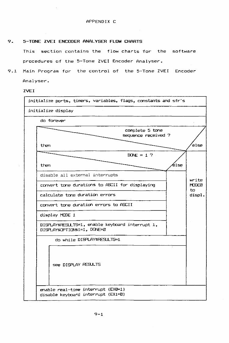
APPENDIX C
9. 5-TONE ZVEI ENCODER ANALYSER FLOW CHARTS
This section contains the flow charts for the software
procedures of the 5-Tone ZVEI Encoder Analyser.
9.1 Main Program for the control of the 5-Tone ZVEI Encoder
Analyser.
ZVEI
initialize ports, timers, variables, flags, constants and sfr's
initialize display
do forever
complete 5 tone
Lsequence received ?
then
IXJ\E 1 ?
~then
disable all external interruptswrite
convert tone durations to ASCII for displaying I'1JDEeJto
calculate tone duration errors displ.
convert tone duration errors to ASCII
display I'1JDE 1
DISPLAY$RESlLTS=1, enable keyboard interrupt 1,DISPLAY$CPTI0\l$1=1, IXJ\E=0
do while DISPLAY$RESlLTS=1
see DISPLAY RESlLTS
enable real-time interrupt (EXeJ=1 )disable keyboard interrupt (EX1=0)
9-1

DISPLAY RESULTS
D--key p..-essed ?
~(display MODE 2 ?)
then
do while DISPLAY$OPTION$l=l
DISPLAY$CPTION$2=l
display MODE 2
do while no option for MODE 2 selected
display MODE 2
IF 1 I 2 I 3
--- display MODE 3 ;z(N - next ?)
then ---------do while DISPLAY$OPTION$2=l
display MODE 3
do while no optic:n for MOOC 3 selected
display MODE 3
IF 4 I 5 I 6 I 7
IF 1
then
display freq. digit?(MODE 4 ?)
else
call DECODEIJ$TCJ\E
do while MODE 4 ..-equi..-ed
display I'1JDE 4
clea..- keypad va..-iable and exit
9-2
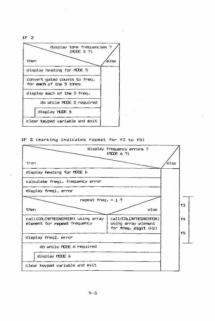
IF 2
~c~(MJIlE 5 ?)
t~ el~
display heading for MJIlE 5
convert gated counts to freq.for each of the 5 tones
display each of the 5 freq.
do while I"1JIlE 5 required
Idisplay I"1JIlE 5
clear keypad variable and exit
IF 3 (marking indicates repeat for f3 to f5)
display frequency errors ? j(I"1JIlE 6 ?)
then
display heading for MJIlE 6
calculate freq1. frequency errOr-
display freq1. error
eq.
~t~
call (CPLC$FREQ$ERR(R) using array call (CPLC$FREQ$ERRCf{)
element for repeat frequency using array elementfor f~. digit (Hz)
display freq2. e ....ror
do While I"1JIlE 6 required
I display I"1JIlE 6
clear keypad variable and exit
9-3
f3
f4
f5

IF 4
then
tone durations ?(mIlE 7 ?)
else
display tone durations
do while mIlE 7 required
display mIlE 7
clear keypad variable and exit
IF 5
display tone duraticn Errors
do while I"lJDE 8 required
display I"lJDE 8
clear keypad variable and exit
9-4
?
else
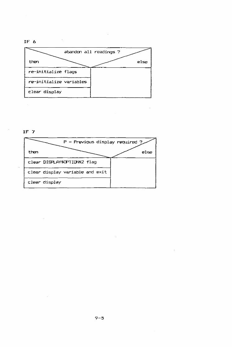
abandon all readings ?
else
IF 6
then
re-initialize flags
re-initialize variables
clear display
IF 7
clear DISPLAY$OPTI0N$2 flag
clear display variable and exit
clear display
9-5

9.2 External interrupt ~, performs real-time selcall analysis.
INTRPTfII
disable any further IN"l"RPT~ interrupts
disable keypad interrupts
data change flagged ? Athen
delay for 1ms
read port, store in TRlE$FREQ1
delay for 1ms
read port, store in TRlE$FREQ
TRlE$FREQ1TRlE$FREQ;L
then else-increment frequency order
init. timer 1 for 5lZIms frequency gating period
ensure frequency counter CH=Q..=0
case digit ~ 1 2 3 4 5 6order skip
enable further INTRPT~ interrupts (EX~)
enable keypad interrupt (EX1)
retum from interrupt
CASE 1
init. timer ~ for 1ms interrupt (1st duration)
enable timer ~
enable timer 1 - gating period for freq. 1
enable CR to measure freq. 1
save value of freq. digit 1 in FREQ$DIG1
9-6

CASE 2
stop timer '"
init. timer '" far 1ms interrupt (2nd duration)
save 1st tane duratian value
clear tane duration variable (E1...FPSED=0 )
enable timer 121
start gating period for freq. 2
enable PCA counter to measure freq. 2
:--------=:::e r::=--------::then else
FREQ$DIG2 = FREQ$DIG1 save freq. digit in FREQ$DIG2
repeat freq. 1 in error calc.
CASE 3
stop timer '"
init. timer '" far 1ms interrupt (3rd duration)
save 2nd tone duration value
clear tone duration variable (E1...FPSED=0 )
enable timer 121
start gating period for freq. 3
enable PCA counter to measure freq. 3
:--------=:::e~then else
FREQ$DIG3 = FREQ$DIG2 save freq. digit in FREQ$DIG3
repeat freq. 2 in error calc.
9-7

CASE 4
s top timer III
init. timer III for lms interrupt (4th duration)
save 3r-d tone duration value
clear tone duration variable (ELAPSED=lIl )
enable timer III
start gating period for freq. 4
enable PCA counter to measure fr-eq. 4
~one r-ec:::----------::then else
FREQ$DIG4 = FREQ$DIG3 save fr-eq. digit in FREQ$DIG4
repeat freq. 3 in error calc.
CASE 5
stop timer III
init. timer IZl for 1ms interrupt (5th duration)
save 4th tone duration value
clear tone duration variable ( ELAPSED=lIl)
enable timer III
start gating period for freq. 5
enable PCA counter to measure freq. 5
::---------:::er~then else
FREQ$DIG5 = FREQ$DlG4 save freq. digit in FREQ$DIG5
repeat fr-eq. 4 in error calc.
9-8

CASE b
stop timer I2l
save 5th tone duration value
clear- tone duration variable ( El.AF'SED=I2l)
reset frequency no. pointer
reset received digit order flag
set DalE = 1, to display results
9.3 Real-time duration timer interrupt.
TIMERIII
1F1ZI cleared on interrupt veetoring
increment tone duration counter
initialize timer reload value
return from interrupt
9.4 Real-time frequency count for each frequency digit.
TIMER 1
stop Capture Register counter
stop timer 1
increment order of received frequency
case 1ZI skip
case 1 store counter value in 1st freq. variables
case 2 store counter value in 2nd freq. variables
case 3 store counter value in 3rd freq. variables
case 4 store counter value in 4th freq. variables
case 5 store counter value in 5th freq. variables
clear Capture Register counter (D-l=CL=lZII2l)
return from interrupt
9-9

9.5 Keypad interrupt, stores key pressed on keypad.
INTRPT1
delay far 1ms
read key--<:ode fram keyboard encoder and store
delay to allow hardware to settle
read key--<:ode fram keyboard encoder and stare
~~then else
save key--<:ode inKEY variable
retum fram interrupt
9.6 Initialization of display an power-up.
DISPLAY$SETUP
delay for display busy flag
enable display
write initialization instruction
remove enable
9.7 Locate address where character is to be displayed.
DISPLAY$ADDR
delay far display busy flag
enable display
write display data address
remove enable
9-1121

9.8 Display a cha~acter at previously defined display address.
DISPLAY$CHAR
write to display data register
delay for display b..1sy flag
enable display
delay for display b..1sy flag
write ASCII byte to display
delay for display b..1sy flag
remove enable & ~egiste~ select
9.9 Calculate tone du~ation er~o~ fo~ each of the 5 tones.
CALC$TDUR$ERR
~tone du~ation - 7fZlms ?
then else---~ati~then else
sto~ 121 to FI/IJ$ERR sto~ + to sign sto~ - to sign
sto~e 2I1lh to sign calc. +ve I. er~~ calc. -ve'l.. error
compute remainde~ compute ~inde~
~ound off remainde~ ~d off remainde~
store in FIN'PERR sto~ in FlmERR.
9-11

9.1~ Initiate the displaying of MODE 1.
SELECTSDSKEYSMSG
clear display
initialize display start address
initialize no. of chars. to write to display
call D$KEY to execute function
9.11 Write display MODE 1 to the display.
DSKEY
initialize display address
write I'1JDE 1 to the display starting at
the initialized address
9.12 Initiate the displaying of MODE 2.
OPTIONSDISPLAYSl
clear display
initialize display start address
initialize no. of chars. to write to display
call OPTICN$rx:NATICNH to execute function
9.13 Write display MODE 2 to the display.
OPT I ONSDONAT IONSl
initialize display address
write MODE 2 to the display starting at
the initialized address
9-12

9.14 Display the f~equency digits fo~ each of the 5 tones.
DECODED$TONE
clea~ display
initialize display address
w~ite MODE 4 heading to the display
w~ite QUIT$MSG to the display
init. display address fo~ freq. digits 1 - 5
w~ite each ASCII keq. digit to the display
9.15 'A-Quit' message fo~ various MODES of displa~
QUIT$MSG
initialize add~s on display
w~ite 'A--a.lit' message to the display
9.16 W~ite MODE 5 heading and initiate display of f~eq. no.'s.
FREQ$HEADING
clea~ display
initialize display address
w~ite MODE 5's heading to the display
call FREQ$IX::N'\nCN to w~ite freq. no. 's
write QUIT$MSG to the display
9-13
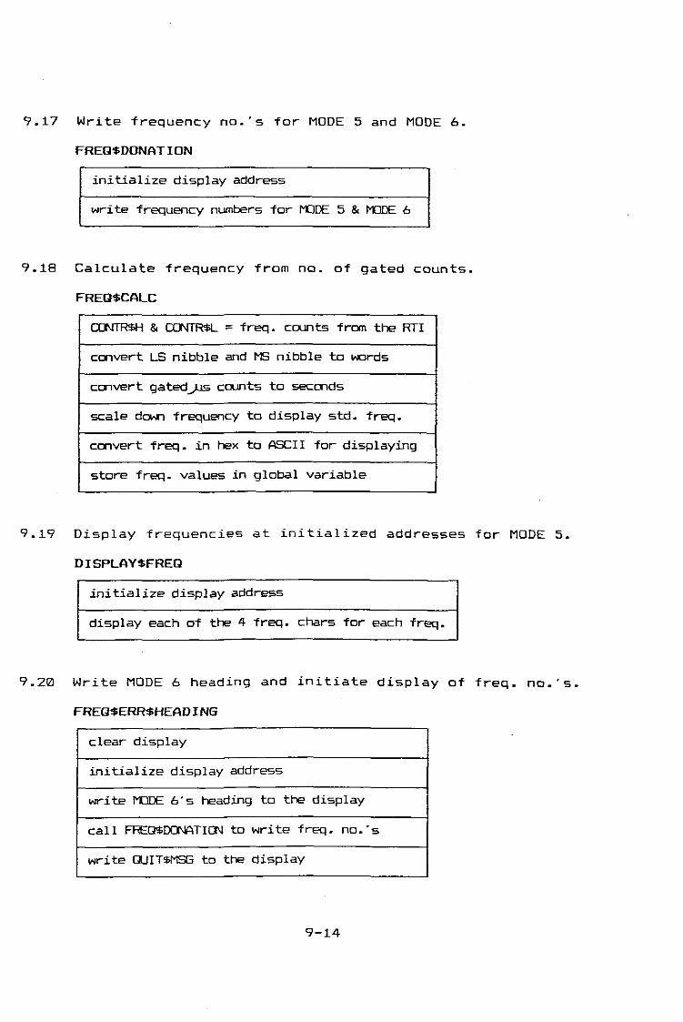
9.17 Write frequency no.'s for MODE 5 and MODE 6.
FREll$DONATION
initialize display address
write frequency numbers for I'1JDE 5 & I'1JDE 6
9.18 Calculate frequency from no. of gated counts.
FREll$CALC
CCNTR$H & CCNTR$L : freq. counts from the RTI
calve-rt LS nibble and MS nibble to words
ccnvert gatedJlS counts to seccnds
scale down frequency to display std. freq.
ccnvert freq. in hex to ASCII for displaying
store freq. values in global variable
9.19 Display frequencies at initialized addresses for MODE 5.
DISPLAY$FREll
initialize display address
display each of the 4 freq. chars for each freq.
9.20 Write MODE 6 heading and initiate display of freq. no.'s.
FREll$ERR$HEADING
clear display
initialize display address
write I'1JIJE 6's heading to the display
call FREQ$IJCN'\TI(J\1 to write freq. no. .s
write QUIT$MSG to the display
9-14

9.21 Calculate f~equency e~~o~ fo~ each of the 5 tones.
CALC$FREQ$ERR
(X]\fffi$H & CCNTR$L = f~eq. counts from the RTI
COlvert LS nibble and MS nibble to wo~ds
Ccr1vert gated.fJS counts to 5eC01ds
obtain standa~d f~eq. of F$DIGIT from a~~ay
~meaSU~edf~. std. f~. ?
then else
~>~then else
sto~ OOh to F$DIG1 sign = +ve e~~~ sign = -ye e~~~
sto~ OOh to F$DIG2 e~~o~ = meas. f~eq. error = stand~ f~eq.
sto~e 2Qlh to sign - standam f~. - meas. f~.
~<~then else
~OOXthen lse
calc. 'l.. error error >= 1%
sto~e in F$DIG1 sto~e in F$DIG1
error < 1% canpute r-emainde~
compute remainde~ sto~e in F$DIG2
sto~e in F$DIG2
9-15

9.22 Display the computed parameters for MODE 6.
SHOW$FREQ$ERR
initialize display address
display +/- error
write F$DIGl to display
write decimal point to display
write F$DIG2 to display
call F'ERC$DISPLAY (write 'l. sign to display)
9.23 Display ''l.' character used in MODE 6 and MODE 8.
PERC$DISPLAY
L = 31
do while L < 32
write ' 'l. . character to display
L = L + 1
9.24 Initiates the displaying of MODE 3.
OPTION$DISPLAY$2
clear display
initialize display start address
initialize no. of chars. to write to display
call CPTIQ\I$!XJ'i"lTIQ\I$2 to execute function
9-16

9.25 W~ite display MODE 3 to the display.
OPTION$DONATION$2
initialize display add~ess
w~ite MODE 3 to the display sta~ting at
the initialized add~s
9.26 Display MODE 7 heading and analysed pa~amete~s.
TONE$DURATIONS
clea~ the display
initialize a~~ay pointe~ to display I'lJDE 7
call T(JIE$DlRAT$MSG
w~ite ·t1=· to display
call DISPLAY$O-M
call msi'.DISPLAY
re-initialize a~~ay pointe~ and display
tcne du~aticns 2, 3, 4 and 5
w~ite . A--O.lit· to the display
9.27 MODE 7 heading.
TONE$DURAT$MSG
initialize display add~ess
do while MODE 7 heading not complete
I w~ite MODE Ts heading to the display
9-17
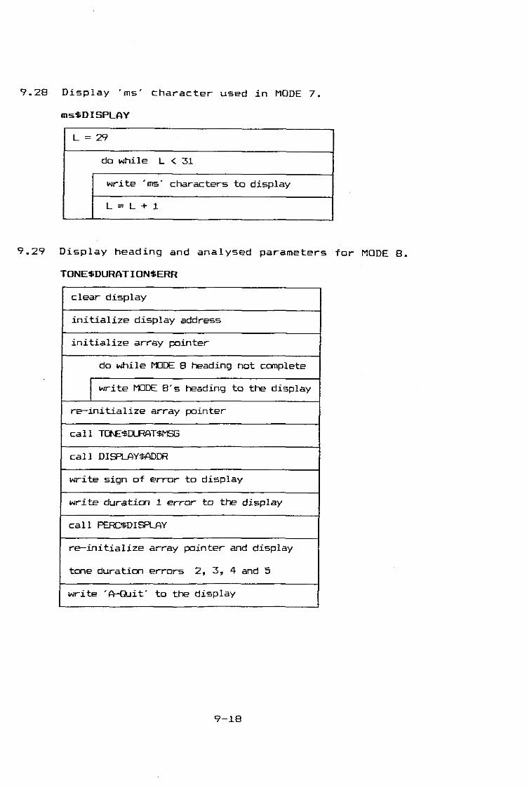
9.28 Display 'ms' character used in MODE 7.
ms$DISPLAY
L = 29
do while L < 31
write 'ms' characters to display
L = L + 1
9.29 Display heading and analysed parameters for MODE 8.
TONE$DURATI ON$ERR
clear display
initialize display address
initialize array pointer
do while MODE 8 heading not complete
Iwrite MODE 8's heading to the display
re-initialize array pointer
call TCl\E$IJl..RAT$MSG
call DISPLAY$AI)DR
write sign of error to display
write duration 1 error to the display
call PERC$DISPLAY
re-initialize array pointer and display
tone duration errors 2, 3, 4 and 5
write 'A--Q..lit' to the display
9-18
A P PEN D I X D
5 - TON E Z V E I E NCO D ERA N A L Y S E R
5 0 F T WAR ELl S TIN G

APPENDIX D
10. 5-TONE ZVEI ENCODER ANALYSER SOFTWARE LISTING
The following pages represents the software listing of the
5-Tone ZVEI Encoder Analyser PLM-51 program.
1~-1

DOS 3.30 f038-N) h/Yi-51 V1..2COMPILER INVOKE] BY: C:\PLM\PL~:l.EXE \PL~\PRDJECTS\ZVEI.PL~ rEBUG RGX{LARSEi
lVET aa
06/16/92 PAGE
SGFTwAR£ZYE I
ct~clafe eq literally 'literally'
$nu1istSincluce{RE6252.DCLitlist
LISTINGEriCuDER
FuR THEAN~LYSER
PR06RAl; VARIABLES
declare { L, DI6$GRDER J FREu$DI61, FREU$uIEt, FREG$UI63, FREg$DIS4,fREi1$fJIoJ, T_uLiRi, iJfU,~2, T_fUR3, TJHJR4, TJfUR5, TJnJRHT1,T_UURHT2, T_GURHT3 J I_DURAT4} T_llURHTJ, ELAPSED, KEY)
c2claf2 DUR$ERRsMSB1, DUR$ERR$LSB1, DUR$ERR$~SB2, DURiERR$LSB2,UUR$ERR$~SB3, DURtERR$LSB3, DUR$ERRiMSB4, DURiERR$LSB4,
10
declarE CQNTR1$H, CO~TR1$L, CCNTR2$H, CDNTR2iL, CDNTR3iH,CDNTR3$L, CDNTR4$H, CCNTR4$L, LUNTRJ$~, CONTRS$L )
ceclare DQ~E~ DISPLAYiRESULTS, DISPLAY$OPTION$l, DISPLAY$8PTIGN$t,REPEAT$FRE]$l, REPEAT$FR:]52~ REPEHTiFREQ$3, REPE~T$FREa$4
nyte !!;~in
de[13r~ DUR$~SB1, DURsLSB1, DUR~~SB2, DUR$LSB2, DUR5XSB3, DUR$LSB3,UUR$~SB4, DUR$LSB4, DUR$~SB5, ilCR$LSB5, SrSN, FIN$ERR,T$DUR4Tl$ERR, T$DURAT2iERR, TSDURAT3$ERR, T$DURAT~!ERR,
T~JjRAT5$ERR, PGS$NESl, PuS;~E62, PGS$NES3, POS~~E~4! PGS$NE65 j tit: ictat~
It ZVEl std. freq.declaf~ STDFREQHABLE (11) \lfGrd cCH1:;tnt \2~OOn, 10M}, 1160D, 1270D, l-t:J0J,
l5:jOj, 16701, IB2iJD, eOOOG, E200J,260(;D!
It dati! change flag it
E~ 'I) CN e;~ •, , ,;:;:,,! '0 :;=-r eq 1-, ,
/J display inst:-uctiGns
if
iflHSP$ON$GFF eq 'GCM' J LCDHNSr eq '2GH' ,LCE$DATA eq 'OROH',
FOREVER E~ 'whil~ 1E
10-2

FL!~-51 CO~PILER IVEl
:t DISF'LAYJ
lMESSAEES I
06/16/92 PA8E 2
15 declarE! MESSA6E$1 {45} tlyt2 ccn":;tant {'REady To R~[ei\[2ZVEr 5iqndl •• ,Key Tnn:;:aitter') ;lb declare MES3RGE$2 f4bJ nyte [Qn5ta~t i'Signal KEceivedSelEct D-Key fDrDis~lay BptiDflS')17 declare MESSAGEi3 (20} byte constant ('Decoded DigitsA-!hit'l ;18 de::1are XESSASE$4 (33) byte [onst-~[!t {'Tone nliratianstl=t2=t3=t4=tJ=ffis~ '} ;19 declarE ~ESSA3E$5 {141 hyte (Qnsta~t {'Duration Error'} ;20 declare ~ESSHEE~6 {49j byte constant ('Select:- C-Nextl-Tone Digits2-Freq.3-Freq. trrof" ;21 declare ~ESSH6E$7 {64} byte constant {'Select:- C-Prev.4-TonE DuratiansS-Duraticn Error6-Guit Readings');22 declare MESSAGE$8 (29i byte constant ('Tone Freq.{HzlF!=F2=F3=F4=F5=')23 dEcla.re filESSASa9 (is) byte constant ('Frequenc'f Error') i
REAL-T ME iNTERRUPT PROCEDURES
24 2 INTRPTO: prQcedure interrupt 0 lising 2. j
declare{TRUE$FREG 1 TRUE$FREG1} byteIt ext. interrupt to process each'* of the ::i-teines
26 227 2
2830 331 3
no = offEH :: eff
[all time{1!]} ;TRUHFREGl = shr ({PI ~nd iSH) ,3 j
It disable all 2Xt. interrupts
11
39 4
37
411....'tC
43444546
49
51
4
•,
,o
6t6,o,o
,Q
66t6
THl = 3CH ;TLl = UAFHCH = O!}HCL = f)l)H
DIS$ORDER = DISsORrER +do case DI5iORDER
THO :: OF CH j
ILl) :: 17HiRe: = 1 ;!Ri = 1 j
eR = 1 :FREG$GI81 = TRUE$FREG
TRG = U
TU) = PH ;T_uURl = ELAPSEDELAPSED = COH,RO = 1 ;
10-3
Ii 5!)~"; ti:lin,; windowIt for freq. gatinqJ* reset freq. cG~nter
It case I)
n caSE 1
It far 1st ton2 duratio1It s t~r t to;;e tUiaticr; ti:i\erIf start g:lti~q peri;J1 far freq1.It enable PC~ etr. ta ~Eas, fre~l.
If save fr2q. digit
n fur cnd tGne du;-atioTIli save l~t tDne cur-aUrin Hlu2It clear tQn~ duratiG~ variableH start tone dlir~tiDn tiiliEr
t!I111
I1
I1t!I1I1I1I1I1J!
1111liIfI1I111

PLfM-51 CGMPILER
,,0 6.,i'.J.
59 iu
M'; "62 7
63 "b4 "65 7
66 0,
'" 7'::11
68,0
69 i
70 671 672
,0
73 674 675 676 6"" 6: I
on "10 ,B(} 7n. 701l"!'"i 7DC
83 "I8~ 7''j:=
06 6
l"!"'! t0 ,B8 6r-. .. 507
9:) !:.91 0
?2,CS
ti,., 6;~
" 67'1'
!}~ 6
96 798 "99 "
lGu101 '1i(J2 "103 "104
,Q
l,'\~ L.i.t.}-...! '-'
106,c
107 .j
108 6lf1=1 6110
,!:'
111 6
IVEI
Ht ;eR =
if TRUE$FREu :: QEH thefi do]FREGDIG2 = FREG$DIGl ;REFEAT~FREQ$l :: set ;eflC! ;
else dc ;FREGtDISc :: TRUEtFREu
do j
TRO = GrHO:: OFCH J
TUj=17H;T_UUR2 = ELAPSEDELAPSEL~ :: OOHIRQ ; 1 ;TRl :: 1 ;eR = 1 ;
FREQJI83 = FREG$DIG2 iREPEAT$FREQ$2 :: setEriC j
eIs-~ d'J :;FREQ$DI53 :: TRUE$FREG
end
ca. iTRO = 0THO :: eFCH :;TLO :: PH ;T_DiJF:3 :: EL~PSEn
ELAPSED :: OOH ;IRe; :: 1TRl :: 1eR :: 1 j
i f TRU::FP~J :: /)EH then dQFREGDIS4 :: FREQ$DIG3 ;RE;E~T$FRE]$3 :: set ;
end
do.IRO :: 0 ;
TU) :: PH ;T_uUR4 :: EL~PSETI
ELAPSED :: 00HTRG :: :
10-4
fJb/16i92
It St.Ft g!ti.r\g ?Fi.act far fre;ic,It e~~blE peA ctr. to sedS. freq2.
n rep-eat tone received?It save previous freq. digit/, cautrol flag used during freq.It error calculatiains
It Sin~ freq. digit
If case 3Il stop tone- duraticHl ti~er
It tiler reload v~lue
n filr 3rd tGll~ dura tiOit
fl save 2nd tone duration ',a-lueIt clear tmi2 duration variableii start tone dura Uon tiillerIt start gating period for freq3.!* enab le peA ctr. to seas. freq3.
It repeat tDn~ received?It save ~rE¥iotis freq. digit(f contral fiag used during freq.It error cl1culatioins
It c.:Ei~ 4H stGp tone duraticm ti~er
1* ti~er reload valueIt for 4th tone durationit SaYE 3rd tone duntion valueIt clear tan!? dura tio!i v;r i~b leIf start tone duntiol! ti!!~r
/, stlrt g~tiITg peried for freq4.!i enable F'L~ etr. to meas. freq!r.
If r2~;1t tJ~= r€:eiy~d ?/. s~y€ preiiclis fr2q. oiqitIt cantra! fl=g uS2d during freq.It ErrDr !:al:ulati;Jins
It n::e 5" 5 tr!~ tQ!!2 dun ticn tLiei
It tiier reload vali12It for 5th tone GUi2tiofJIt. save 4th tm!2 GijratiDn 'iaheft clear tone 1~iration variable'* start tonE durdtian tim.er
PAGE "0
t!1/
1/IIl!tf
1I
1/1/IIl!1Il!l!1/I1
I11Il!1/
II
t!1Il!IIIII1IIII1I
l!II1Il/
1I
1Il!l/l/1Il!l!

F'Lft!-51 CC:1FILER
i12 61~ 1 6
114 7116 7117 7118 '1
119 7
121 ~
122 6
T'!~T
LE.!.
TRl :: 1 ieR :: 1 ;
if TRUE$FREQ ::: uEH thEn duFREGDIG5 :: FREGiDI64 j
REPEATtFREQ$4 ::: setend ;
els2 da ;FR£G.53 [S5 ::: TRU[fFREtlend
end ;
06/16/92
Jj start qating periud fur treq5.It enab le peA [tr. to ilIeas. freq5.
!l r~jJ=a.t tone receiv"ed ?1* save previolis fleq. digitIf cantral flag used during freq.1* error calculations
It save freq. digit
PAGE 4
1/1/
Ift!1111
t/
135 2 HO ::: Qfl
124125126127128129pt'!
131
133
66bb6666<•
3 end;EH::: Oli
end
do iTRO ::: 0 j
TJWR5 ::: ELAPSEDELAPSED ::: Omi j
CURRENT$FREQ ::: OHDI6$CRDER ::: [)DONE ::: 1 j
end
If case 61* stop tone duration tilHefIt save 5th tone dura UDn HIue/i c1e~r tone duration variableIl reset fleq. no. pointerIt reset digit order flagH flag tac~ground task,n ready ta disp lay rest! 1ts
1/111/11111/1111
11
136 end INTRPTO ;
137 2'! - - :
142 2-143 3145 3
[all ti>TIE(10) ;KEYIN ::: rEi UP3 and OFijn j ;
{;~1l ti~2fli)! ;KEYINl :: ntrt(P3 and OFOH j ;
if KEYIN ::: KEY 1Nl then do
ii allcr# nard~.:re to SEttle/i and ;ask aff bits
1* key :: key pressed en keypad
11
l!1/
1/
14b 3 end147 End INTRPT1
148 2149 ::150 2151 2-
153 2
155 2156 2~.:-r: r-U! ,j:
158 3159 4.160 4161 4162 4-
163 4.
TlrERO: proc2dui2 interrupt GSlr.] 2ELriPSED ::: £LHPSED f 1 ;THO :: 1}FCH ;TLO = 17H
TI~ER1: pro:::e,:ure 1\1 tern!~ t 3 liS in;eR=!);El :: C; ;CURRENT$FREQ = CURRENT$FREG +
do CdS~ CURRENT$FREG
CUNTRl$L ::: CLend ;
da ,[DNTR2$H :: CH
10-5
fl iil.!ratiaTI ti~er interrupt/t hs ca'J:rr teTf* tiffiEf r210;1 v;lueIt for lfS interrupt
il int"2rrupt ta sto,E gatedfi freq. CDun t
!* freq. [DUn t far each af t~e
It 5 fre>:;. digitsl* case (i
li Easelft freql high counter valliefj freql la" (Gun t~f value
H ca.se2It freq2 high cQunter value
1/U1111
11111/
1111If1111
1111

Ft/M-51 IVEI 06/16/92 P~GE
165 c,
166 4
167 416S 4169 4170 4
.... , 4ill
1'"1." 4I<
173 4174 4
."'!~ 41 i..J
i76 4~ ... .., ,if! ,J "!,, 41 IQ
1"0 3I,
180 2181 2''''':Jl!j....
CONTR2$L :: CL
GD J
CmHR3$H :: CHCONTR3$L :: CL
end ;
do ;CGNTRtt$!i :: CHCUNTRtt$-L ;:: Cl..
end j
CfifiTR5iH = CHCnNTR5$L ;:: CL
endend
CH=Q1JHjCL ;:: OOH ;end TIMER!
{i fr~q2 lo~ CQUTIt~r value
If case3H fl~q3 hig~ countEr value{i freq3 IOIt [Gun ter value
n fraq!t high GH.m t2r \fi!lue/. treqf ID~ CDUiiI2r value
It caseSn. freq5 higil cm.m ter value/* freq5 low counte. value
Ii clear peA cmm ter
i/
1/1/1/
If1/If
tt1111
If
I BEN ERA L P RDe EDURES I183 2184- 2185 2136 2'M 2~OJ
fl""" 2lOQ
189
190 2191 2192 2193 2<1;1. ,11"! 0
J I'!l: 2i 'L!
196
197 0
198 2,91 2200 0
201,0
202 2203 2204 t.
205 :i
"206
'"'~-_ ... EClj!
2fJB 2209 2
DISPlAY$SETuP : prucedure{LCD,INSTjttEclare {LeD) INST} byte;call tilli2HCOi j
PO ;:: PO: or LeD j
P2 :;; INST ;PO ;:: PO alid ODFH
end DISPL~¥$SETUP ;
DrSPLAY$ADDR : prGcedure(LCD,ADDR}decldfe (LeD, ~DDR) byteC-:i 11 tiili2 t1 OO} ,Pi) : PO m" LCfl ;P2 = ~DDR ;P!) ;:: PO ana nc UlCiH
end DISPLAY$ADDR ;
DIS?LA¥!CHAR : prGc~dure{LCD.DATA)
declare (LeD, DATAl oytePO ;:: PO Of BOH ;call ti~::(10j ;Pr) ;:: PO Of LeD ;
call tii2(1O) ;PO = pr} and 1FH
~TId OI5PLAY!CHAR ;
CALC$TTIUR$ERR : proc2durE tT_DURAT; ;declare [T_DURAT, SC~L~ j =,te ;c2clare iERR, Q~EF, ~~;~~=~~;) ~crd
10-6
If display init. on power-up
If enable displayn instr. to initialize/t re~a¥e enaoie
iI allo. LeD to ."ttl.It en~ble displayIt. DD addressIf re~Gve errajIE
It displ cnH. at a:dr.
t: enable Gispl~y
/l allow (EspIal ti~e t:l -settleIt nrit~ ascii biteIf aIla\ot dis~lay ti:ii~ tu settleJ~ fe~aV2 2TIaJle ;nd RS
!I1/
t!
1/tfIf
*1
If1/1/t!It1/!I
1/

PUM-51 CO~PIL£R lVEI 06/16/92 PAGE 6
1I1I1I
1I
11
1It!
1Iif
1I
IfI './
II11
1I
111IIf
IIII
IIIfIf1/11
ifit
n any tune .duration errDr 'J
'* flO ~!if liu sign required
11 yes "it +'i~ errorIt cal[til;t~ Xerror
Il round off remainder
It display ~ODEl
It round off re~ainder
If -ye error{; calCI! late ~ eirur
It initiate cisplaying OT MOrE 1If clear dispI~l
It display nODE 1n iUessage l'iritte!'! tu display/; setup display ~ddTess
it start ~·jM. t nJ. of,; chars. tiJ ~r ite ta disp la'(
/t start add!. ! no. ofn etars. to ljrit~ tn displ~y
it display r.QDE 2It clear di;;la1
Il writes chars. to displayIt based an para~eters passedIl illit. display ;:dress!J jlfr ite ch;.;s. ta di.s) Idf
It MODE 2
iLlJ.\.il
29)
CLR$I.HSP j
15 i
FINERR :: OHSIGN:: 20H
ERR:: (T_DURA; - 46Hi;100FINtERR :: ERR ! 46H ;OVER ~ FIN$ERR * 46H iwuRKiDvER :: (ERR - OVER) i OAH ;SCALE :: WGRKiQVER ! 46H ;if SC~LE ):: 5 then FIN$ERR :: FINtERR+lend ;
else do j
SI6~: ~ 2.DHERR:: (46H - T_OURATJll00FIN$ERR :: ERR ! 46H ;GvER :: F[N$ERR J 46H ;WGRK$QVER :: (ERR - OVER) t OAH ;SCALE :: ~uRK$aVER I 46H ;if SCALE )= :I theli fIN$ERR ::: FIN$ERR+l
end;else aD ;
if T DURAT ) 46H the\'! do .:
l ::: I) ;
Gill n$~·.EY { SOH,
L = 0 ;call OPTrON$DG~ATION$l{ SOH,call OprIGN$1l~N4TIDN$!{0[OHJ
end LHlC$TDURiERR
l=L+l ;
D$KEY : prccedufe{ADDRS J E$PRA~j ;declare{ADDRS J E$PRAM) byte;call DISPLHY$ADDRiLCniINST I ADDRBjdo ~hile L -( E$PRP.ff ;
call DISPLHY$CHARfLCD$DATA, MES5ASE2S(L})L :: L + 1 ;
end
SELECHD$KEHMSc : prGCE<"1Ure ;call rrISPLAY$SETuP(LGD$INST, CLR$JfSPi
DPTION$DDNATIQ~$l : prG[~jufe(ADDRSl E$PRA~)
aecla,e{ADDR.s J £$PRA~) byt':: ;call DISPL~Y$AnDR{LCD$I~ST,A[DRSi ;de ~hi!~ L < E$PRHn ;
call DISPLAY$CHAR{LCD$DAT~, rESSAGE6i(Ll}
ende;:d OPTIDN$DGNATIGN$l
GPTION$DISPLR¥$l : procedurecall DISPLAV$SETUP{LCD$INST,
210 0~
212 00
213 3214 "00'" 3,-.!.,J
216 4218 4219 4-cc>] it221 4222 4'" 4cc~
224 4'" 4c.eo
227 4,,28 4229 4230 4231 4232 4"'':1'' 4I:... ,;j-
234 4236 4c37 0
0
""'QC""'>t
,·Pt". 2C~7
240 ,"
241 2242 ..,
""'1/." 3C"'!'J
244,0
245,,;i
"'Il.lc'tO
""_~ 2C"'ti
248 0c249 2."'I.~," 2.c,i'1
2.-=:1 "252 22Ji
254 2'-'I;""l:' 2c.,J,.,
256 2257 :1'"'-=,'1 .,C,JQ ,259 ::;260 3"",.COL
,,' 2CelC
26-3,c
""ff. 2cc't
265 2~i.L
"l...~"'"
10-7

IVEI Nu'lb/92. PAGE 7
267 2268 2269
call aPTIQN$Da~HTION$l{ 9GH, 36}(ell DPTIDN$VDNATIDNl!lODOH, 49'
end GPiIGN$DiSPLAYsl
Il passed tJ proc. il
270271272
274
GUIT$MSG ; procedurecal! DI8PL~Y$ADnR{LCn$rN5T,OVRH]
L = 14;do llihi Le l <2C i
call DI5PL~¥$CHRR(LCD$DHTA, ~ESSA6E$3{L))
/i display ~-auit
It write chars. tD displ,~1<
11
il275 3276 32.77 1
L = L + Iend ;
end GUITiMSB
278
280
DECGDEDHONE procedure;
call DISPLAYfSETUP{LCD$INST, CLR$DISP)call DISPLAY$ADDR{LCU$INST,SlH)
It display decoded tones'It fnq. digits/l clear displayli init. display' ~ddiess
ilifilil
2B3 3
231 ~
282 3if
if11if'Iififif
ilf/if
Ii write freq. digit "<It irri t. cii5~12Y addressti #T~t~ fr2q. di~ it 3It init. display address/I write freq. digit ,.,It iuiL displ,y ad-dress11 ;jrite freq. digit r
J
It init. display addressJj write fr2q. digit 1It alIa. display ti;e to settle
li display ~CDE 4
L = 0 ;do 8hile L { 14 j
call DISPlAY$CHAR{LCDiDATA J ~ESSASE$3(L})
l = L + 1end ,call a1lIHXSS ;call lliSPLAY$~DllR{LCn$INST ,93Hlcall DISPlAY$GHARlLCDsVATA J (FREG$DI61 Of ZOH))nil ti;eUO} ;call DISPLAr$AnDR{LGntrNST}9JP.~
call DISPLAY$CHAR{lCD$DATA, (FREG$DIB2 Of 30H))call DI5PL~Yta.~DR(LC~!rNST,97H) iL~ll DISPL~~$CHAR{LCD$nAT~, {FR~G$nl~3 Of ~OHi~
call nISPLAr$~aDR(LCDirNSTJ99HJ j
call DISPLAYiCHAR(LCD$DATA, (FREG$DIS4 or 30H)!call D[SPl~Y$ADaR{LCD$IN5TJqBHJ j
call DI5PLAHCHMULCD$DATA, {FREQ$Di65 Of 3DHDend DECODETI$T8NE ;
222
22
291
28S28b
"H·I1~
C7~
289
216297
299
303
2
FREG$DuNATIGN procedure{~DDRS, E$PRA~i
declareiATIDRS! EiPRAN ) bytecall DtSPLAY$AllDR{LCD$!NST ,ADGRSicia ¥thile L { aPRA!'l ;
call DISPLAY$CHA.R{LCD$DATH, ~ESSA6E8$(L)J
t =L + 1End
fi wr He freq. no. for MODE' 5 :; &6!l tu displayIt iiii t. ~i-;?la't ~djr~s.;
If display Fx= ~essage
i/ili!
il
3.07 2308 :J
... ,.., .,~lC .J
313 3
FREu$H£~DINB : pfDceduiE ;call llISPLAyiSETUP{LCD$INST, CLR~DrSPJ
Cell DI5PL~¥$~rDR(L[D$INSTf81H}
L = Q ;
;fa if~iI2 L <14 ;call DISPLHYtCHAR(LCD$DATA, [;ESS~GE$8{L))
L = L t 1 i
Ij ~rit? t2ading fo, MODE 5li clear ~i~~lay
If displ,;y tG~e fr€tf.tHz}
It write tonE freq,(Hz}It tu diSjj1ar
1/1/1/
314 3315 2316
318
2
end
c~ll FREG$DuN~TIQN{90H,
call FREQ$DCNATICN{ODOH,call FREatDGNATIuN(UC9H,
20123i
/l dispI~l '''''-'r"l-
iI 4ispl~y 'F2='11 disp [3Y 'F3='li display 'F4='
t'./il1/il
10-8

PL/N-51 COMPILER NEI 06116192 PAGE B
319 2:320 2321
call FREQ$DGNATION{99H, 29)call QUIT$1'tSS ;
end FREa$~EADING j
It display 'F5:' tl
'"''''''·lee
323324325326..., •.,"'1';'Ci
329
"p..,;,.:J-:J\J
333334
2
""""""""o•
FREGsCALC : prDcedure (CuNTR$H, CGNTR$L ) j
dEclar~ {CGNTR$H, CGNTR$L, FREQ$IN, NEW$DI61,CiJNTRK = doublE(CJNTRiU ;CONTR$H =dOuble{CGNTR$H} ;CGNTR$H = shl(CUNTR~H,8) j
FREG$IN = {CuNTRiH or CGNTRiL} j 05H
F$D!61 ={FREQ$INI3E8H } or 3GHNEWiDI61 =FREG$IN mod 3EBH ;
F$DIS2 =( NEWfDI61/64H ) or 30HNE~$DI62 = NEWiDlfil ~od 64H ;
FiDI53 =( NEW$nr82fOAH ) or 30H ;
FfDIS4 ={NEWiDIS2 lod OAH } or 30Hend FREI]$CAlC j
1* eale. freq. froii no. of ga tedNEWtDI62 ) ward j
It nibble to byte conversion
It bit ianipulatirmIf NB!! V.I.? COUNT t 20/4n 20 :- (DrIVer ts to sec.It 4:- freq ••tilt. by 4 so weIt lust scale down for carrectIl dispiay af std. input freq.It hex to ascii cony. for displ,
It he. to ascii cony. for displ.
It hex to ascii cony. for dispI.
caunts tl
tf
tltlIItltltftf
tl
tl
335 2336 2337 2333 2339 2340 2341 2342
DISPLAY$FREH : procedure{FREG$ADDR, F$DIS1, F$DIS2, F$DI63, FSDI64) ;d;clare (FREa$~DDRJ FtD!61, FiDloc, FtDI63, F$DIB41 byte;[all DISPLAHADDR(LCHHiST, FREG$ADORI It display freq. at correctcall lHSPLAnCHAR{LC!1$DATA, HDI8U If pasitiorr ail the display·call DISPLAYiCHAR{LCll$OATA, F$DIS2i It for MUDE 5call llISPLAY$CHARfLCD$DATA, F$DIG3icall DISPLAY$CHAR{lCD!DATA, fiDI84)
end DISPLAYsFREQ ;
tltltI
343344
346
2
"33
PERG$nI5PL~Y : praceaure{L}declare U.; byte ;do while L <32 ;
call DI5FLHY$CHAR(LCD~DATA, MESSASEi4(L)}
It display 'X' for xaDE 6
It write 'X' to display
tl
tl347 3 L = L + 1 ;348 3 end349 2~d PERC$DISPLAY
350 2351 2352 2
r;~;;; .,';:0..' ,.j
356 3357 3358 2359 2360 2361 2362 2363 2364 2365 2366 2367 2
FRE~$ERR$HEADINS prGc~1ure j
c~ll DISPLAY$SETUP{LCD$IN5T, CLR$JISP}call DI5PLA¥$HDDR{LCu$INST,80HlL = i) ,;
dD ~hile L { 15 icall DISPL~Y$CHHR(~CD$DAT~, nESS~G~$9{L))
L=L+ljendL = 14
l = 17 ,;call FREG$DONATImH9GH, 19)L = 20 ;cdll FREGSDCNATIDN{ODOH, 22)L :: 23 ;call FREQ$DGNATIONfOC9H, 25Jl = cb j
call FREIT!DGNATIDN{99H, 2H)
10-9
/i ~rite heading for MODE 6/; clear di~pl~f
/l init. display acdiess
It writ~ 'FrEquency Error'Il heading to display
/t display 'F1::''* i!Jit. display addressIf display 'F2='
II display 'F3='
It display 'F4:'
It display 'F5='
tltltl
tltl
tltltf
tl
tl
tf

STD$FREG =STD$FREQiTABLE{F$DiGITJ It g~t std. freq frG~ array
SHG~$FREG$ERR procedure (FREQ;ADDR, SIGN, F$uIG1, Ftnr62J ;decl~re {FREQ$ADDR, SrG~, F$nIG1~ FtDI621 tytE il ctispl~y ~QDE 6
c~ll DI.5PUWiADDR{LCD$INST, FREQ$ADDRi II init. display ajjr~ss
CALCiFREtUERR : proc~dlire {CGNTR$H, CDNTRiL J F$:a rGIn ; If ca le • freq. errordeclare (CONTRlH, CGNTR$L, FREGSIN, STD$FREa, ERR ) word ;declare (F$DIGIT, SCALE) byte
CGNTR$L = dUlih12{~ONTR$L) It nibble to byte conversionCQNTRiH =dauole{CGNTR$Hl ;CaNTR$H = s~UcaNTtHH,B1 ; /f hit sanipulatiOITFREG$IN = (CONTR$H or CONTRsLi i Q5H It convert to seconds
it
/1I './
11
11
11
11fI11
11111I
11/1
1Iil/1It/1
PAGE 9
11
f!
11
1I/1
1I
/11I/1
06116/92
between 10 and 100 ?)= U
It qllit ~essag~ for MGuE b
If freq. leas. = std. IVEI11 frEq. digit?fj error::: 0
It error <a
It - error
11 frEq. ;Eas. } std. ZVEI frEq. ?It + error
" error <10 ?If cale. enuf11 use FinIS1 as variables li;itedIt storeIf use FREG$IN as variables li;ited
It dl~plal signI; display e,ror/; display Ce[ilal pointIt dis~laf rElainderIt display units
End
end ;else do ;
if ERR )= OAH and ERR {= 64H then da It errorERR = (ERJU64H l j It errorFtDIGl =ERR1STD$FREG ; It storefREG$IN={ERR-{F$nISlfSTll~fR£~J;tO~H j
FUH62 = FREGHNfSTD$FF:EQ ; It stare
if SCALE )= 05H theTI F$DI62 = F$uIS2 + 1 iSCALE = FREGiIN1STD$FRE9 ;
F$DrS2 = (ERRiOAHJ/STu$FREaFREu$IN = 5Tn~FREQtF$DIS2 ;fREG$IN =({ERRiOAHJ - FREQ$INjtOAH
if £RR <OAH then CD ;ERR = {ERRio;H l ;F~DrGl = ERRISTDtFREG
end ;els2 do ;
SIGN:: 2DH j
ERR:: STD$FREG - FREG$INEnd;
S!6N =if FREllHN ~ STll$FREtl then do
FiUISI =DOHFiDIS2 = OOHend ;
else do ;if FREQ$IN ) STDiFREG then do j
SISN :: 2BH ;ERR =FREGiIN - STD$FREQ
end
zvn
(all llUIT$~SiJ j
end FREG$ERR$HEADING
c~ll VI5PLHY!CHrlR(LCll$r;'T~~ 5I8N~ j
call DISPLAY$CHAR(LCu$DATA, {FfDI61 or 30H)}call nISPLAY$CHAR{LCD$uATA J 2CHl ;call UISPLAY$CHRR{LCil$DATA, {FirrrS2 Of 30H})call PERC$nISPL~Y(31)
erri SHa~$FREa$ERR ;
""P'1 2.,)/jC)
369
370 2"'I':'; ....if l- r:'7" ..,),r;. r:
373 ..r:374 ..
r:
375' 2.... , 2~iQ
377 2
..... 3,,3/Q
380 ,,381 ..,382 3383 3384 ,,..no 4"'D..;
3B7 ,•
385 4'1"l"I 4J:01
390 ,.,..... 4.l1l
3n ,•
393',•
394 4",;!,'<i ,.·.nQ •397 4398 4399 ,
•40u ,.•401 ,.•402 4404 ,.•40S 4406 5408 0
0
409 541f} 0
"411 0
0
412 5413
,•
414 ..,:-
41:1
416 ..,=417 2413 ..
r:
419 2q.£{] 2421 ..
r:I."'''' ..'tc-e r:
4.23 ,r:
424 1
F'L/1't-51 COMPILER

PL!N-51 CG~PIL£R ZI'tI 06/16/92 PAGE H
call nISPLAY$CHARtLCO$DATA, DUR$MSB2)
end j
end ilsillISPLM
L = 17 j
call TaNE$rURAT$~5S(9aH, ca] j
if
ifi/
ififif
11ifif
Ififififif
f!i/
iff!
ifif
11H
11
i/
if
It dis~lai units
1* display units
It. display li~its
If writ2 'tt::'n display 1st tCfi2 GUfatiaTI
/t re-init. array pointerfj ~rit~ It3:: 1
If display 3rd tone duration
ti rE~-init. array painterIi Ii,ite '(2='
/i display 2nd taTIe duratioTI
'* heading for MODE 7
If. display 'is' far HflflE 7
If dispIa), MQDE 7It clear display
If write 'Tane Dura~ions'
fj ta dis~lay
If start addr. l no. efIi chars. to write to displayfi passed to prac.
It display MOnE 3It cledf display
It display tone dlira:tion/i heading for XUD£ 7
If writes chars. to dis~lar
1* based On p~ra~et2rs passedIt init. display acrcrressIt write chars. bJ disphyIl MOD£ 3
'* write ';5 tu display
48163)
call TDNE$DURAT$~S81 aCON f 17; ;call DI8?LHr$CHAR(LCn~DHT;, DUR$~SBt}
call VrjPLfi't$CHARlLrD$D,4TH, DURKSP1Jcall ~s$DISPL~Y(29)
ca 11 DISPLA'{$CH~R (lCNDHT~ J DUR$lSE'2 j
call ;stGISFLAY{29i
L :: 20 j
call TOtJ_aQijR~HMS6U)DOH,231 ;call DISPl~Y$CHAR(LCD$DATA, DUR$~SB3)
call DISPLAY$CHAR{lCD$nAi~, DURtLSE3)call is$DISPLAH29} ;
QPrraN$DaN~TrQN$c : placedure(~DaRS~ E$PR~~l
decIare{ADTIRS, BPRAni byte;c~Ir DISPLAY$AODR{LCO$fN5T,ADGRSldo "hi le L { E$PRArf ;
call OISPLAY$CHARfLCD$UATA, nESS~GE7t(LJf
L=Ltl;
UPTIDNiDISPLAYi2 : procedure ;call DI5PLAYfSETUP{LCD$INST,L = 0 ;call DPTION$DONATIDNi2{ SOH,call OPTIDN!DaN~TIUN$2{QCOH,
call OPTIDN$DGNATIDNi2( 90H,call GPTIDN$DDNATIDNi2{OnOH,
end OPTIGN$DISPLAY$2 ;
end OPTION$DONhTION$2
TONEiDURATIGNS pracadure;call DISPLAYiSETUP{LCD$!NST, CLR$DISPiL = 0 ;call TONE$llURAT$~SS{81H, Iq} ;
Is$llISPL~Y : prQcecturefLjdeclar~ (U byte j
do ~hile L <31 ;call DISPLAY$CHHRtLCll$DATA, MESSAGE$4fL)}L = L t 1
10~E$DURAT$~S6 : prG[erl~re{~DnRS, E$PR~tt}
declare(~DDRS, E$PRH~} byte;call DISPLAY$ADDR(LCD$INST,ADDRSl ;cia whilt! l <. E$PRAt1 ;
c;11 DIS?LAY$CHAR(LCD$D~TA, ~E3SAEE4$(L)}
l=L+ljend;
end TU~E$DUR~r$~gS
425,c
426 2427 ,
c
42B 34"0 ".c, 0
430 "0431 3432
433 0•434 "c435 C436 "c437 2438 2439 2440 1
441 244e 2443 2444 3445 "0446 3447
,0
44~ 1
449 "c450 "c451 3452 ",453 "0454 3455
456 2457 2458. 2459 2
1.1'·' 2'to'"461 2/.r::, 2'tCI...
463 "c
464 246;; 24b6 "0467 "0468 2
469 "c47J} 241 ' 2,1
472 "c/,"''''1 2'tJ,J
10-11

PL/:1-51 CD~PILER ZVEI 06/16!'i2 PAGE 11
!t7ft,c
475 2476 2477
,c
4?B 2
4Ti ,c
4BO,c
481,c
482,c
433 2484
,c
485
486,c
487 2488 2489 2490 3491
,0
lL":'l 3,7~
493 ,0
494 21."<:' 2't1'J
496 0
"m ,c
498 2499
,c
:it)!} 2
<" 2,J!! ;..
<:"i'" 0,,}'.·C "503 2504 2505 2J()6 ,
c50!
,C
r/1" 2<!v!:!
509 2Sir; 2<j! 2..1.1..1.
Jt2 £<="t':l 2JJ""/:.1. e",il"!"
515 2516 0
"517
,c
s=,n 2,1 ...~
519,c
520,c
~~1 2'..';.... 1.
r"'" C·..le£:.
I _:;'\ •L - C.2 ,
call TUNE$TIURAT$~SG{OC9H, 2b} ;call ilISPLAY$CHARiLCU$DATA, ilUR$nSB4jcall OISPL~Y$CHAR{LCD$~~TA!nUR$LSB4)cllI isfliI5PLAY{ct}
L ~ 26 ;call iDNE$DURAI$MS3{99H, 29} ;call DISPL~r$CH~R{L[D$D~TR, DUR$~SBJl
call DISFLAY~CHAR{LCD$DATA, DUR$LSB5l[all iis$DI5PLAH29jcaIl UUIT$I1S6 ;
end TONEiDURATluNS ;
TDNESDURATluNtERR : procedure ;call OISPLAY$5ETUP{LCD$INST, CLRiDISPlcall DISPLAY$ADDR{LCD$INST, 81H) ;l = 0 ;do while L ( 14 ;
call llISPLAYiCHAR{LCD$DATH, ~ESSAGE$5{L}1
l = L + 1 ;end ;
1. = 14 icall TONE$DURAT$~SS(OCOH, 17) ;call DISPLAY$ADDRiLCD$INST, OC3HJcall DIS?LAY$CH~RtLCD$DRi~J PliSiNEG1) ;call DISPL~Y$CHRR(L[DiV~TR! DUR$ERR$~SB1}
call DISPLAY$CHARiLCD$DATA, DUR$ERR$LSBllcail FERC$DISPlAYl31}
L = 17 ;call TDNE$DUR~T$MSG{90H, to} ;call DrSPLHt$ADDR(lCDiINST, 93Hicall DISFLAY$CHAR{LCD$DATA, POS$~EG2)
call DISPLAY$CHAR{LCu$DHfA, uUR$ERR$~5B~1
call DISPLAY$CHAR(LCDSDATA, DUR$ERR$LSB2lcall PERC$uISPl~Yi311
L : 20 ;call TGNEiDURAT$XSS{ODOH, 23} j
call DI5PL~Y$AUDRiLCO$rNST, OD3Hjcall DISPLAY$CHAR{LCD$D~TA, PGSSNEG3lc~ll Dlj~LAY$CHAR{LCD$DAT~J DUR$ERR$MSB3)call DrSPLHY$CHAR(LCD$D~TA~ DUR$ERR$LSB3icall ?ER~~DISPLAY(31)
L ~ 23 ;call TONE$DURAT$nSafOC9H, 26; i[~ll DrSPLA.¥$~DDR(LCDiINST! uLeN!call uI5PLRrtCHARlLCD$DHTA, PDS$NE54)call DrSPL~Y$CHAR{LLD$nATA,DURiERRSMSS4)call DISPL~¥~CHhR{LCD$up.T~, ilUR$ERR$LSB4)call PERC$DISPLA¥(31)
L : 26
10-12
if re-init. arra, painteril .rite 't4='It display 4th tune duration
II displa, ",its
It f~-init. array paiuterIt writ~ . t5='If displdy ~th tufie dardtiGIT
1I display unitsIt quit cessage far MODE 7
It display MODE eIt clear display1I iniL display address
It write 'Duration Error'n to display
It ioU. array paintern write 'tt:' to display1I init. display address11 display sign f·)f t1If display 1st tDne duratiDJ error
It display units
/i re-init. array pointErIt write 't2=' to displayIt foft. display addressIi display sign for t2/t display 2rra tcn~ duration error
It re-init. array painterf1, write 't3:' to displayIt lait. display a'!dre-3sIt display sign far t3It displ~y 3r1 tone duration errer
I. display llilits
It re-init. array painterit wiite 't4:' tn displayIt intt. diSpLay addressIf displ~y sign for t41* display 4th tune duration error
It display units
It fe-in it. array pointer
fIIfIf
/1I1if
I1If
11I1If
iffI
I1I1/1IftI
t!
t!I1II*ttI
/1
I1I1IfI1It
I1
I1I1I1t!I1
It

PL!~-51 COMPILER IVEI 06116/92 PAGE lE
~"",
..lC>.! 0
524 Cc;"'.e Co"lC,J
52,5 E!i"l"l ,""Cl C
5ca c529 t530
call TGNE$nURAT$~SS{99H, 291 ;call DISPLAY$ADDR{lCD$INST, 9CHJcall DISPLAYSCHARfLCDtDATA, PQS$NEG5icall nI5PL~Y$CH~R{LCDtD~TAJ rUR$ERR$~585j
call DISPLAY$CHAR(LCDiDATA, DUR$ERR$L5B51call PERC$DISPLAY(31lcall atHHMSG ;
~nd TGNE$nUR~TluN$ERR
/i write 'tS::' ta display t!H hit. displa1· address if1I disel.y sign for t5 I1If displdy 5th tone duration error If
It display units HIf quit ;2ssage for ManEat!
N TAL SAT I DN
If wdag off, external cGunt ifp enab. CF::C ifIt rlin aff, (a~~. capt. flags cl~ar il'* disabled t!It disabled l!
I; display:: alp, loijer nibble spare t!H ref. freq ! sig i/p set to ilp H1I port t all alp far disp a.jdr. I data HIt HHu ~ niB ait. func, 3.4 -} 3.7 ~eybd 'f
l/
1/
I1If
I1If
If
Iftl
trig. HHIfI1I1
It 50~s g~ting window
it iuit. tane du:aticns
!J order ef tone sequenceIt repeat freq. flags
It current frEQ. being ieasure~
It in it. [Dun t reg for fn:q. leas.
If init. freq! high CDunter valueIf init. freql 11J~ counter nlu2
It tiler 0, t eode 2, auto reloadIl Eoer 0, 1 Off, INTO l lNTl leve1It no serial ca~ls. implelented1I glooal, TO, H, £la l EH int's. en.ol.If INTO higher priority TO, INTl, Tt lONerIf pQ~er down, idle made inhibited
Cm~TR2$L =
niUD :: 000l0001BTCON :: OOOOONlOBsemi:: 0 ;IE :: 10001111BIF = 01HPCGN :: 0
THt _ .,r-u •Iru - ,jl."ll ,
TU :: OAFH j
CURRENTiFREti :: ~rl
C~uD :: 000001103ceaN :: f)OH j
CC~FM2 = OOOOOOOOBCCAPM4 :: 01001000B
TJi!JR4 :: OHT)JJR5 :: OH
[ONTRUl = QOHCGNTR2$H :: DOH
PI) :: OOH ;Pl :: GFFH;P2 :: OOHF3 :: QCH
T_uURl :; OHTJUR2 :: OHT IiUR3 :: OH
CH :: QOHCL :: OOH
CGNT~'3$L = fjrjHCmHR4$H = OOHemHRt.$L = 0011CQiiTRS$H :: OOH
DI6SQRDER :: er ,
REPL~T$FRE~$l =0REPEAT$FREG$2 :: 0REPEAHFREG$3 :: 0
531 1<"...!.:le.
533534
535<" 1'"'~o
537 1538 1539540
541 1S42· 1543544
545 15"46 1547 1548 1549 1
550£;:I:;"!,-,,",,,,
552r::-l:;"')o"l,J-"
554&;!;"l:;"•.!o,,!>o/
556r:,.~7
558t=l::1"\...!o,,!7
56;}5~1
562-563564
<-< 1;,JQ;,J
<- , 1~lJQ
56756-8
10-13

0\/16/92
,•
., -:>•
:, t:~E ti~E ~uratl:R ::JnterI1 :."li2I,zo 2,1 Ilag.
iiI;
,. 11itialize PDWer-U~ Cnnditi3n Ot ri5~laY.~ _ r
:74 !1/
/l .jis~lay en~ble::i~ :~str. iRS = ~), :2 lines f 518 Dets! 8 bIt i/call DI5PLp.Y1SETUP(LSD$INST~ FUNC$SET; ;
576
f!
!
l!
1/
I!
i; se1:a11 ree. ! re~dy for dis:lavfl init. cisplav a:dr2ss
is :~5 d2bcE~ce pe;:~1 2fro~ ::5p,(!~~~; lIt l1e;: to ;'5::'i CG!'l"i':fS1Cl1 If
n far tane duntiJ!1 2 jj
If display 5CD£ @
L=L+l;end !
~~ ~ril2 L 4~:
:a11 Jr:?_ArsC~AR(LC~ij;~;, ~ESS~BE$l\L.
[ill Dl5F~~Y$;nDR;~CD$rNST! SlH: ;'- ::: ~ ;10 MhilE L ( 16 ;
:alI DrSPl~V$CHAR(LCD$J~rA, r.ESSF.SE$l{Lj}
call DISPLAY'ADDR(LCD$INS~, 0C1H)do ~hile L ( 3~ ;
~alI nrSPLAY$CH~R{LCDfnATA, ~£SSteE$~tlJ!
L=L+l:
T_DUE~Tl = i~}L_R:+~)-~4H f:UPirSSl = n-_jjRAL;'J;1-; Jr 3~h
rUR;_SE~ = :~_JJR~T: ~G: ~2t! QT Si~
T_jL~~:2 ='_DUR2+3 ;DUR;~SE2 = tT_DURATZ!2A~; or 3~K ;
da FJREVER ;:77 2
57B ,0
520 3591 3582 l
583 4564 4585 4586 ,
v
587 :,
588 4589 !
=.:,,'- ,"-.:·~2 ~
~~.~ ;er, l":~5 l
59t .,
=:;7
5~'~.,
:tU .,
6~i.,
6~Z 3t~3
tZ4 .,__,
6i5 3616 .,
6~7T
"
10-14
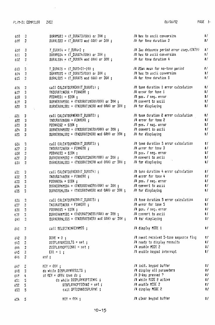
PL/n-5i CQMPILER ZVEl 06/lbf92 PAGE 1;.
DUR$MSB3 = {T_DURAT3/0AHi Ut 30H ;DURtLSB3 = (T_llURAT3 lad O~N} or 30H
TJWRHT4 = f_uIJR4+3 ;DUR$nSB4 = (T_DURAT4/CAH} Of 30H j
DURiLSB4 = (r_DUR~r4 mad GAHJ or SaH
T_DURAT5 ={T_DURJ+3J-19HDUR$MSB5 = {T_DURAT5/0~Hi or 30H j
DUR$L5B5 = (T_DURAT5 ffiGd OAHi or 30H
call CALC$TDUR$ERRIT_DURAT21T$flURAT2$ERR : FIN$ERR ;PDSSNE62 =SIGN ;DUHSERR$nSB2 =CTtDURAT2$ERR/OAH) Of 30H ;DUR$ERR$LSB2 = IT$DURAT2$ERR !od CAHI or 30H
If:rififif
ififififif
ififilIfif
uUilU11if
if
ifififif
II
ifififHil
r/IIH
ilifififII
It res~t receiv~d 5-tane sequ~nc~ fl~g
It ready to display ressultsIt enable MODE 2It enable keypad intErrupt
It display ~CDE 1
Jf iait. keypad bufferli display all para!etersIt D-<ey pressed ?
It while MODE 2 activeIt en~t!e ~GDE 3li display MODE 2
If eSiS mean tor no-tone periodli hex ta ascii conversionIt for tone duration ~
It tone duration 2 error calculationIt error for tone 2Ii pos. I neg. errorli convert to asciiIi for displaying
It 3i5 debaunce period error ([j;j'jp. larO) t!It hex to l1scii conversion ifIf for tone duration ~ tI
li clear key pad Duffer
1* hex to ascii conversion if/j far tane duration :1 fl
It tonE duration 5 error calculationIt error for tone :iIt pas. f neg. error1* convert to asciiIl for displaying
lJ tone duratinn it error calculationIf error far torre 4li pos. I neg. errorIf convert to asciiIi for displaying
It tone duration 3 error calculationIt error tDr ton~ 3It pus. I neg. errorIf tanvert to eS[iili for displaying
It tone duration 1 error calculationli error for tone 1li pos. I neg. errorIt convert to asciiIt for displaying
,30H
call CALC$TDUR$ERR{T_DURAT1)T$DURAT1$ERR =FINiERR j
PGS$NEBl =SIGN j
DUR$ERR$MSBl = fT$DURAT1$ERR10AH) or 3QH ;DUR$ERR$LSBl =fTiDURAT1$ERR lad OAHJ or 30H
KEY = OQH
call SELECT$D$KEYiMS8
[all CRLC$TuUR$ERR{T_uURAT5iT$DURP,T5$ERR ~ FINiERR ;POS$NEG5 =SIGN j
DUR$ERR$~SBS = {T$DURAT5$ERRIOAHl or 30HDUR$ERR$LSB5 = {T$DURAT5tERR mad O~H} or
call LHLC$TDUR$ERR{T_DUR~T3)
l$rURAr3~ERR =FIN$ERR ;POSiNE83 =SIGN ;liURfERRtHSB3 = (T$DUR~T3$ERR!OAH} or 30HDUR$S~R$LSB3 = (TtDURAT3$ERR @od OAH) or 30H
DDNE=O;DISPLAY$RESULT5 = SEt ;
PISPLAY$DPTIDN$! =SEt
call CALC$TDUR$ERRtT_DURAT41T$DUR~T4$£RR ~ fINtERR ;POSiNES4 ~ SIGN ;DUR$ERR$MSB4 =(r$DUR~T4$ERR/OAHJ or 30H j
nURiERRlLSB4 = fl$TIURAT4$ERR mad QAH) or 3CH
KEY = {)OH j
da while DISPlAYiRE5ULTSif KEY = GFfH thEn da ;
ca while nISPLAY$OPTlnN$l j
nrSPLAY$GPTrONfc =set;call GPTIONiDISPLAYil
Ell = 1Err1 ;
b08 31'" ,.... '17 "610 0
~
611,", 4 ''I ,
Oli: 0
613 :3614 36'· 3lJ
616,"
617,"
618,"
619,"620 3
<0' ,QC.!. "b2~ 3'" 300':-:>
h24 3625
,"
6~6 362? ,
"bea ,"
62~ "-
"630 3
631,,
l"i"i 30';;;:'
J"i"1 ~,
U':!.J ,634 3635
,•
1",
~J!:!,
637,J
638,,::
639 3040 3
641 0
"
H·E 0
"643 :::644 3645
,,646 {;
647 E:648 3tA9 4651 •J,,;, <u",c J
053 •"654 5
10-15

da while (KEY () OFH and KEY () IFH and KEY () cFH and KEV () OBFHI j
KEY = OOH I1 clear key pad buffer 11end ;
If freq3 error, ~GDE b 11
It (ale. freq2 error %1
It freq2 errur, rODE 6 it
11
1111
If1111
PAGE 1~
If freql, gated cQunts HIf disp. fregl. nODE 5 11
11 A-Quit ?
It r~p!?lt tune? flIt error using 2600hz fI
It repea t tone? jj
It error t!-5iTI'~ 2600hz H
It -freq5, ga ted CQun ts t IIf disp. freqS. MODE 5 II
If clear Key pad buffer if
11 display rODE 6' 11n 'Frequene'( Error' tIIt cale. freql. Error l'ft freql error) nDDE 6 lr
It eale. freq3 Error il
11 freq3, gated caunts fl11 disp. freq3. ~ODE 5 11
11 display ~DDE 5 ?I1 'Tone Freg.(H:)'
It display ~ODE 4 ~
It yes !!11 A-Quit ?
11 freq4, ga ted CDun ts 1111 disp. freq4. ~ODE 5 11
11 freqc, gated calints 1111 disp. freqc. ~ODE 5 11
It clear key pad buffer II
06116/92
call FREG$CALCfCGNTR4$H, (DNTR4$L) j
call DISPLp,Y$FREG (OGCH, FiDIS1, F$DI62, F!DIG3, F$DIS4i
call fREGiCALCfCGNTR3$H, CQNTR3fLl j
call DISPLAYiFREG (Oll3H, fiDIS1, FfOIS2, F$DI63, F$DI64~
call FREufCALCICDNTR1$H, CflNTR1SL) ;call nr5PL~f$FR£a (OG3H, FtDI5!, FfDI62, ffDIS3, F$DI541
raIl FREO$CALC{CGNTR2iH, CGNTR2iL) j
call DI5PLAY$FRE~ {93H, FiDISl, F$DI62, F$DIS3, F$Dr64l
end ;
call FREQ$CALC~CDNTR5$H, rONTRS$LI j
call DISFLAY$FREg f9CH, FiDIG1, F$OIS2, FiDI63, FiDIS4)
KEY :; OOH ;
if REPEAT$FREGil :; set then dotall CALCSFREQiERR{CGNTR2$n, CQNTR2~L, 10nlend;
els~ cr,] ;call C~LC$FREG$ERR{CGNTR2$H, CONTR2$L, FRE~tnIG2)
end j
call SHG~$FREG$ERR{92H, SIEN, FtDIS1, FSDIB2) ;
if REPEAnFREG$~ :; set then do ;call CALC$rREGtERR{CONTR3$H, CCNTR.3$L, lOD)end ;.
else dQ ;call CALC$FREG1ERR{CGNTR31H, CQNTR3SL, FREQtDI53Jend;
call 5HC~$FREG$ERFHC1J2H, SIGN, FiDIal, nDIS2l ;
end ;KEY:; (H}H
du while KEY {) 3FH
if KEY:; QfH then do ;tall DECOOED$TONE
if KEY = IFH then do j
call FR£USHEADIN6 ;
if KEY = 2FH th~fj do ;call FREG$ERR$HEADIN6 ;call CALCiFREQ$ERRtCGNTRlfH, CCNTRliL, FREGiDIS1)call SHOW$FREG$ERR{QC2H, Si6N, F$DIS1, F$nrS2l j
do fthile KEY {> 3FHKEY = DOH
end j
KEY " OOHend ;
PL!~-51 COMPILER IVEI
65:i 6656 6657 L
"
6SB 666lj 6661 7
662 "I6'" ,
Q, ,6&4 666S 6
666,0
hMi 6
669 6670 6
6"' 6"672 6
673 6674 6
675 6,.,;
6CiQ
A"" 6_if
J~i"i 6Olll
679 7680 76Bl 7682 6683 6
684 66!.:!L 6';.Ii.'
687 6688 6
6B9 "IJ". 7Q71.
692 "I693 7694-
,,69J "I696 6
m 7'"" 701"1
700 "I7(,1 7702 7703 77fJ4 b
10-16

It clear keypad buffer *1() 4FH and KEY {} srn and KEY 0 OBFH and KEY G 6tH) ;
It clear keyp~d buffer t/End ;
KEY :: (jOH
tIt!If
iftlIf
11
PAGE I,
/i [le;, key pad buffer *1
It display ~QDE 8 ?
it rOES : ~
Ii A-Qui t
/l A-Guit ?
It aaandon rEadings? tfIt clear all variables t!
/l clear keypad buffer il
It return to MODE c? tlIt disao 12 ~aDE 3 tlit clear k~y~ad buffer tf
It display MODE 7 ?It yes !!It A-Oui t ?
/l freq4 error, MODE b 11
1* freqS error, MOnE b if
11 MODE 3 IfIt ~hile nODE 3 active *1It display MODE 3 il
/l repeat tone 1/It error using 2600hz *1
11 caIe. freq5 error 11
If repeat tone ilIt error using 2600hz tl
11 ca le • freq4 error *J
C6/16192
:: COH j1:',....",..~l
if KEY = 4FH then aD ;
do ~hile KEY <) 3FHKEY :: fJOH
call TGNE$DURATIONSdJ while KEY {} 3FH
if KEY =5FH then do ;cdll TDNE$DURA.TIDNiERR
end ;
CGNTR2$L = OH
end;rEY = COH
KEY = OOH ;dC! while (KEY
KEY = OOH
if KEY = OBFH then rla ;VISPLHTfGPrraU$E :: 0
end ;
if KEY = 6FH then doCGNTRl$H = OHCO~TR1$L :: OHCONTR2$H ::: OH
endKEY = DOH ;
end ;
call uPTlu~$DISPL~Y$2
do .hiIe KEY () 3FHKEY = COH
end;KEY = OOH
if REPE~T$FREG$3 = set thEn do ;call CALC$~REQ$ERR{LG~TR4$H, CONTR4$L, lOOlend ;
elsE do ;call CALCiFREG$ERR(CONTR4iH, CG~TR4$l, FREQiDIS4)enD;
call SHU~$FREG$ERR(OCBHJ SIGN, F$DI61, FiDI821
if REPEATiFREG$4 =set then do ;call CRLC$FREG$ERRlCDNTR5$H, CDNTRS$l, 10V)end ;
else da ;call C~LC$FREG$ERR(CGNTR5$H, CONTR5$L, FREQSOlfi51errd ;
call SHD~$FREG$ERR(9BH, SIGN, FtuIG1, FtDI62}
if KEY = OBFH then do ;do while DISPLAYiOPTIGNt2
end ;
PLtM-51 CQXPILER ZVEI
70S707708709 7710· 7"'I'~ 7ill
712 6
713 70'" 7110
716 7717
,I
718,I
7!9 7720 6
'0' 0lel I
722 7723 7724 67"'~ 6u
7'26,c
723 7'7"" 01C-7 I
730 700' 8I~l
732 8.., ...... 8j~,)
734 a"1"1 n/,)0 C
737 90;"'''' 'iJJQ..",n 9t.:J1
740 0c741 a
742 a744 13745 9746 9747 9748 8749 a
"'Il:'!'l nI L!~~ C
"'1:'''' aJ.JC
753 B7}4 a
"-" n{.JJ 0
757 a758 8759 8,.,/A n'0') C
10-17
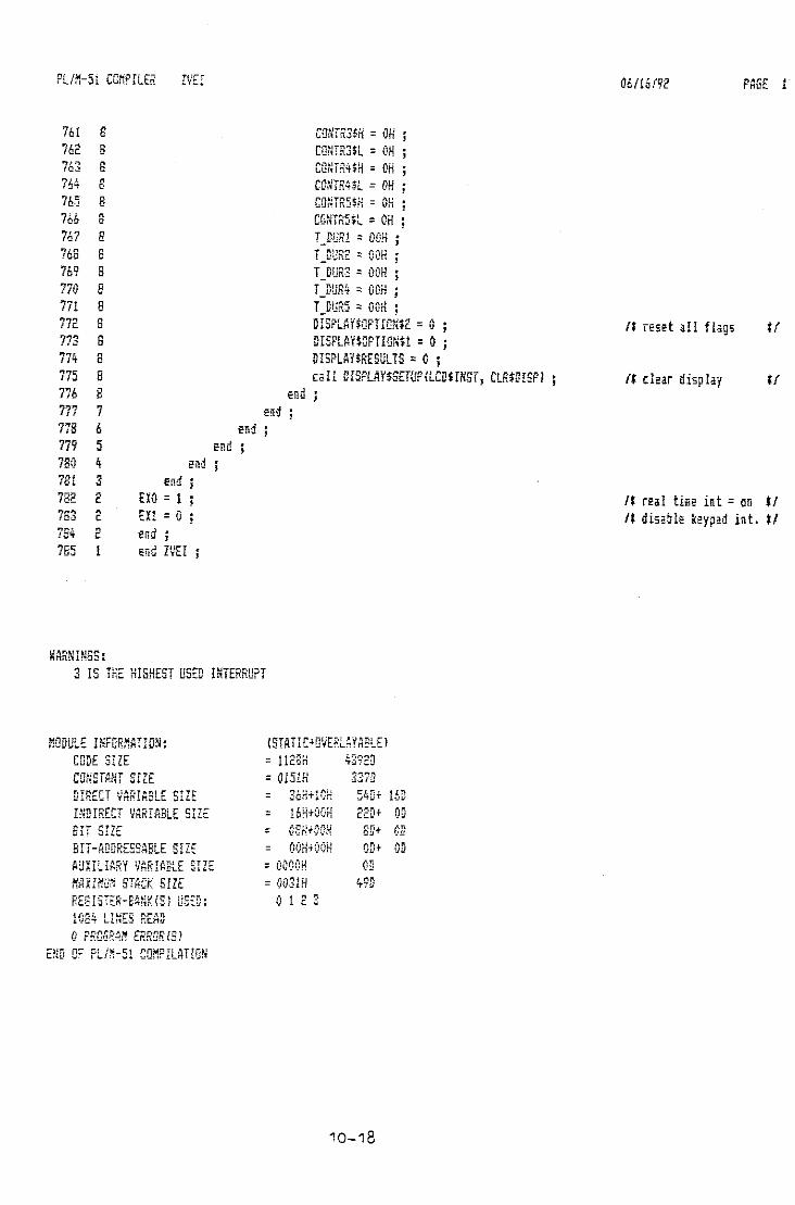
11 real time int = on HI1 disab le keypad in t. If
PL/I1-51 CuHPILfR [VEl
761 8762 B763 8764 n
0
7b5 B766 n
0
767 8768 B7f/1 n
0
?IQ 8771 Bnnn BI le
773 B774 n
0
775 B776 8 end777 7 e!ld778 6 end779 5 end780 4 end781 3 en,j782 n nQ =c783 n m = 0c784 n end ;c785 I end ZVEI j
CfWTR3$H = CHCONTR3K = OHCuNTR4iH = OHCGNTR4$L =OHCGNTR5H; = OHCONTR5K = OHT))iJR1 .: DOH
T_DUR3 .: OOHTJH.lR4 ;: (iOHT)ilJR5 ::: Out{ ,DISPLAY$QPTIG~$2 =0DISPlAYiOPTIGNil =0 ;DlSPLH¥$RESULTS ;: 0 ;call nISPLAYfS£TUP{LCDffNST J ClR~arSPJ
06116(~2
If reset all flags
II clear display
PAGE 1-
If
if
WARNINGS:3 IS THE HIGHEST USED INTERRUPT
(STATICtDVERLAYABLE)= i i28H 4392D
MuDULE INFDR~AIION:
CanE SIZECUNSTMiT SIlEDIRECT ~ARIHELE SIZEINDIRECT VARIABLE SIlEHT SIZEBIT-ADDRESSABLE SIZEAUlILIARY VARI~BLE SIZE~AXrnUH STHCK SIZEREGISTER-B;NK{Si USED:1084 LINES READo PRaG2A~ ERRGR{SI
END DF PLiM-51 COMPILATION
= 0151H.: 36H+IOH;: 16H+OOH
= (J(iH+OOH= OOOGH= (;i).31N
() 12':'
"'l'''P''!1\·l·~ /J.i
54D+ 16D22D+ ODBil+ ODOD+ ODOD
49D
10-18

A P PEN D I X E
5 I M U L ATE D D A T A C H A N G E
F LOW C H ART 5
5 I G N A L

APPENDIX E
11. SIMULATED DATA CHANGE SIGNAL FLOW CHARTS
Flow diagrams for simulator software generating the data
change signals on a 8~31 simulator board.
11.1 Timer interrupt to produce 7~ms time delay.
TIMERlII
then
first interrupt ?(PASS = ~ ?)
else
11.2
init. timer ~ to interrupt
after 4.465 ms
set PASS flag = 1
Main program flow.
MAIN
set STROEE flag
clear PASS flag
init. timer ~ to interrupt
after 65.535 ms
init. ports, timer ~, variables, flags & SFR's
~~then
debounce switch
do while I (= 6
initialize timer ~
start timer ~ running
cutput 1 ms pulse
do while STROBE = 0
wait for 7f2l ms interrupt
clear STROEE flag
11-1

A P PEN D I X F
S I M U L ATE D D A T A
S 0 F T WAR E
C H A N G E S I G N A L
LIS TIN G

APPENDIX F
12. SIMULATED DATA CHANGE SIGNAL SOFTWARE LISTING
The following pages represents the software listing of the
simulated 1ms data change pulse generated every 7~ms.
12-1
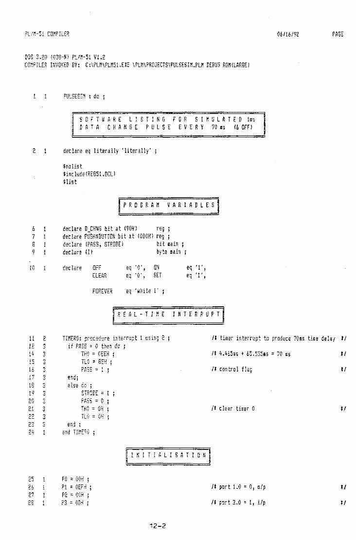
?L!~-5i CQ~PILER 06/16/92 FAGE
DGS 3.20 !038-N! PL!M-51 Vl.2CGHPILER INVOKED BY~ C:\PL~\PLn51tEXE \PLM\PRGJECTS\PULSESIM.PLM DEBUG ROM{L~R6E}
PULSESIM ; da
LIS TIN 6i S Q; T ~ ARE, nATA CHAN6 E P U l S E
F GR S! MU L ATE n 105
EVE R Y 70 IS (6 OFF)
2 1 dEclare eq literally 'litErally-'
$nGlist$inclurle{REfi51.DCLJ$list
Ipo""" ••I n I.' t; r. Ii 1I VARI ABL ESIb declare u_CHNG bit at {90Hl reg ;7 declare PUSH$BUTTu~ bit at (OBOHi reg j
E declare (PASS, STROBEl bit Ilain ;9 decla.re (!) byte ma.in
10 declare OFF eq .{) , aN eq 'I ,CLEAR 2q '0' OrT eq ", ;J=.: 1 ,
FOREVER eq 'while 1 i
I NTERR UP TI
end;elsE IT;:; ;
STROBE: ::: t
/; timer interru~t tu produce 70:15 tiE2 delay tI
11
11
I1
H contral flag
1* 4.465iS + b3.535iS =70 ~s
It c: lEi!f tLf:1Ef 0THO = OH ;T~ (, _ I'.ll •!,-''- - '.1:, )
PASS = 0 j
THG = OEEH ;TLO =8EH j
PASS = 1
End
11 "c12 ::;; t. 3; 0 31":
16 21
.,Z,
18 319 32(; 0
21 .,0
22 3,..,., .,C-1 ~
"',1.e'!
• .. ·"'LI"ATI"·'!lalllh'J l.Il4i,
26 Pi : OEFn ; /i part 1.0 = 0, nlp27 P2 =OGH ;28 Il part 3.0 = 1, tIp 11
12-2

PLlM-5;' CQMP ILER PULSESIM 06/16/92 PAGE
2930"1u,00')i:.
00.:.,:,
34
35 tro;,,:\a
'".:.:
380".:.-:
41 243 244 346 347 448 4
50 45i Er
52 453 4
56 4~7 453
3
61
ICON : OOOOOCOOBSCON:!);lE : 10000010BIF' = OOHPCuN : 0 ;
nw :: OOHTLO : ODH
PASS: () ;STROBE:: [)I = 0 ;
M~ I N PRO fi RAr.
da FOREVER ;if PUSHiBUTTON :: 0 then
ca 11 tilile f250} ;if PUSHiBUTTON :: Q then da
I :: (I j
do while I <:: 0THO :: OH ;TLO :: OH ;IRO = 1 j
D_CHNS :: 1
ltCtmS :: 0 ;do while STROBE:: 0encr ;STRDBE : (!
1=1+1;end
~n:1 PULSESI~
1* tiffier (I iUode 2 au to re load/f timEr 0 initially offit no serial CG]~S. i~ple~ented
It global, TO interrupts enabledn iiQfllHl priority af interruptsIf pORer dilWTI, idle zede inhibited
li Hili!?: f I~g!! flag to initiate data change pulseIf data change pUlSE counter
If denounce switchIt iriitiat2 start of sequencEIf ~hen pushcuttail is pressedI; ~en. five 70~s periodsIl ensure tillle! l) is rese t
It shrt timer Ij
It ~Hit far tiIiEr in t.
/t reset flag far interruptIt prEp~ir for nExt data change
Ifl!l!1/l/tf
l/l/tf
if1/l/l/J/
1/l/
l/1/
1 IS THE HIGHEST USED INTERRUPT
CCTIE SIZECONSTMH SIZEDIRECT vARIRBLE SrZEINUIRECT VARIABLE SIZEBIT SIZEBIT-ADDRESSHBLE SIZE
188 LINES READo PRuGR~~ ERRGR(S;
END uF PL/~-5i CQ~PILATrQ~
:: 007AH:: 00;)0)-1:: 01H+OOH= (jOH+OOH: 02H+OOH:: OOH+OOH:: OOOOH: OOltH
i) 2
12f:u
ID+ ODant ODcD+ ODOD+ ODOD
17D
12-3

A P PEN D I X G
S I M U L ATE D D A T A C H A N G E
REP RES ENT A T ION
S I G N A L

APPENDIX G
13. SIMULATED DATA CHANGE SIGNAL REPRESENTATION
The following page ..-ep..-esents the data change signals
gene..-ated by a simulato..- boa..-d using a 8~31 mic..-o
cont..-olle..-.
13-1

hp 3 topped
1
- t.V fharJ.:ers -~-----~--~---,------.,.---..,----...,..--.....,.--~. 5'1#;0 .on I
:rata cier,ge {.
( 2) (3)~I
(5 ) (6I
Tone 1i
Tone: 2 Tone 3 :Tone Tohe 5
b:::::::::~;;!.~!:.. =::;::::::::~~:::;::==, ::;"~j~:::::-::::;::::Jl:::::;_::':::::::±;:;:::::::::::±::::::::::= _ "" t m5 r k e r 3 __
'---'---.;.-i.---~;:~,---"---"'".,.---'----;---:,----'----iloff ;a.oM Ill.t ,
'---'--L-.c---i1----+---'--'---'----7---'-----'----ir- start Iilarl,er -,I "",! ·1:- s:~gs~;·:,d~1,J; I
'-_--'---.;-'-_-'-,__-'-_--,-_--'-__,--_-'-_-+-_-...;1 !,- Stop mert8r --.
'----"---'---i----"---:--c-'----'-----'-----'-----'----:-----'t' ~ll;;;iA..!~j1e=-@ I,-25('.000 ms 0.00000 s 2:50. OOiJ ms - • ~
50.0 il'iS/tti~l
step mBrKer: -i63.000msstart marKer: -93.0000ms
Tone duration =d8 ~ t;5, t: -70.0000rrr2l/deite t: 14.2857 ~
Data Change sigria!s generated by simulator board usinga 8031 microcontroller
13-2

A P PEN D I X H
MOD E IZl T 0 MOD E 8 D I S P LAY FOR M A T
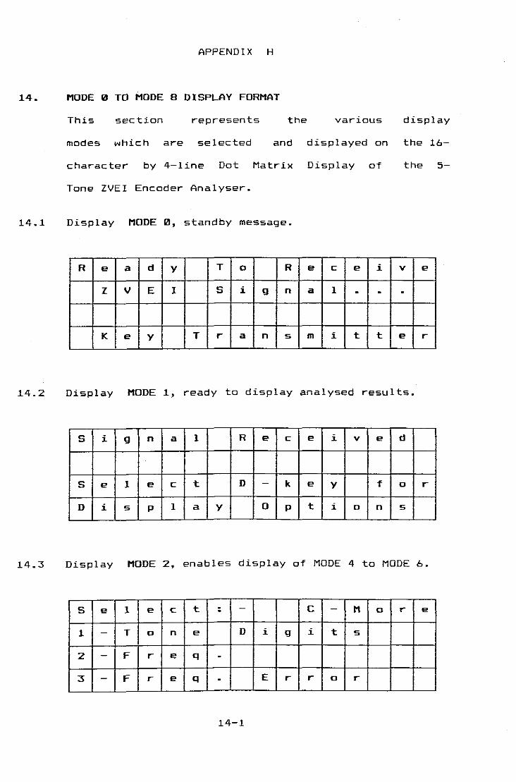
APPENDIX H
14. MODE 0 TO MODE 8 DISPLAY FORMAT
This section represents the various display
modes which are selected and displayed on the 16-
14.1
character by 4-line Dot Matrix Display of
Tone ZVEI Encoder Analyser.
Display MODE 0, stand by message.
the 5-
14.2
14.3
R e a d y T 0 R e c: e i v e
Z V E I S i 9 n a 1 . . .
K e y T r a n s m i t t e r
Display MODE 1, ready to display analysed results.
S i 9 n a 1 R e c: e i v e d
S e 1 e c t D - k e y f 0 r
D i 5 P 1 a y 0 P t i 0 n s
Display MODE 2, enables display of MODE 4 to MODE 6.
S e 1 e c: t : - C - M 0 r e
1 - T 0 n e D i 9 i t 5
2 - F r e q .
3 - F r e q . E r r 0 r
14-1

14.4
14.5
14.6
Display MODE 3, enables display of MODE 7, 8 and MODE 1/1.
5 e 1 e c t : - C - P r e v -4 - T 0 n e D u r a t i D n s
5 - D u r a t i D n E r r 0 r
A - Il u i t R e a d i n 9 s
Display MODE 4, showing typical decoded digits.
D e c D d e d D i 9 i t s
1 2 3 4 5
A - Il u i t
Display MODE 5, showing typical tone frequencies.
T 0 n e F r e q . ( H z )
F 1 = 1 III 6 III F 4 = 1 4 III III
F 2 = 1 1 6 III F 5 = 1 5 3 III
F 3 = 1 2 7 III A - Il u i t
14-2

14.7
14.8
14.9
Display MODE 6, showing typical frequency errors.
F r e q u e n c y E r r 0 r
F 1 + III , 1 7- F 4 - 1 , 2 7-
F 2 III , III 7- F 5 + III , 1 7-
F 3 - III • 5 7- A - (} u .i t:
Display MODE 7, showing typical tone durations.
T 0 n e D u r a t: .i 0 n s
t: 1 = 7 III m s t: 4 = 6 9 m s
t: 2 = 6 8 m s t: 5 = 7 III m s
t: 3 = 7 1 m s A - (} u .i t:
Display MODE e, showing typical tone duration errors.
D u r a t: .i 0 n E r r 0 r
t: 1 = + III 3 7- t: 4 = - III 4 7-
t: 2 = - III 1 7- t: 5 = + III 2 7-
t: 3 = III III 7- A - (} u .i t:
14-3

A P PEN D I X I
W A V E FOR M 5 0 F TON E
F R E QUE N C I E 5
DIG I T

APPENDIX I
15. WAVEFORMS OF TONE DIGIT FREQUENCIES
The following pages ~ep~esents the wavefo~ms of the Tone
Digit F~equencies fo~ digits ~ to 9 and the ~epeat tone.
The wavefo~ms we~e measu~ed at the output of a FXl~2LG.
15-1

,r.=-'-...·:.,';~~_~··,."'7':":,:,:..-..: ...:J",·"t----:----:--
.Jr....:...,y.;...,.,;.:'.~_.~.- ....._~~t..._,o.:-;:_..J
.::.t markers --',., f f tu!",";.. I_. . I
·_...:.....---iir-:!
'--'. ;
~"+--:-"""""-¥-:---;'''''-+-~:-'.'~'3-",-+-:--:-;.~-:..~.~~.-:--;-~:.r-~: :-_:_:_._.-J: I : . -'- _
.~
r----'--.-"---.---=-------.;..--------'-~.-.-
qn jiJ:!
-jOG,OCtG~ -~ - .-. -. ".
l.)". V'_.".)!,)l)- :::.
'.1..1) • u US"":11 v
)(- S t;J.p ti=.:ii-kei- --,
.; i if ··~.jb~!'~"j!:.;:; i ,
ae ita t·1/(181 ta t: 9. 32536kH:
Waveform representint; a Tone Dit;it of "0"
,";_'_' ._.,._._ ..__.. 1- :t._-----~ !
....~._--_. __.._..:..+..._-----.-;..-._-_._.;
:1
i ;-------.~,.... -·-·---:-.--·-·-··-··,-1·-----·---·--···----·,··-··--·
'1
,,_-,-,_._--:_.':'..,._.....,.._ ,-"_.c-_:..._' ~ ...:.__'-_:.. .c_._.•• _ ..",•._:-._~ ••:•••.c._~-:_.'-:.._._. _'.-.-- ~_•.----~--"-~---,.
'-"-"-'---' :.__._._--,,--.~---_.,.
.._._...._--_._ .._-_.._,. .,.....---- ...- .._-,
, ,
.'
-. - -..- ... --.--.-' .. --,::- .. •.. 1 '. ''''.. , "_0;:", ' t ,~.~ .-,.~.,'-._.~""; , ._.... -_.....:;,
dei ttl' f.: -.235.I)t)tJU£
Tide} ta t: ~.2S532kfu
Waveform representint; a Tone Dit;it of "1"
15-2

•
•,,• ,,••
, ,,, ..
\.' OO,)OG ~
; ._._._-'-__..;.i..__'-__....i.....
, ~V markers ---,
11 ·~--...,;.;.t M.iiJ& on :
-......;.---.c,'1'-----!L.....-..1.---rir,..~:->~·:+~~>i : I"'~~~'~+""-'~i: r,.!..
. .,..'
;~J-,~~.~-~~c....H_L'_'~H~'~-;-~ i : ..~-,-,-......;.-,-,l~~,~ i' ,,- fit iflorkers ---
.-:---~-.--.,;_t.--.....,----..:..--~j} off £D.i ..ssi.; t ;1•• =__.._._-__.!; I .
;: : - '3t.~rt. MArko::r
__-'~.;,~_._,'-_-..:..--_;l.i,' ~~~~i~.~t;~·_~-~·,~.~~·;~$~·~2'~?~'I,1•1-;; I: l
delta t: -lj6.000u81/d8! ta t: ,:;;. 6Z963kH:::
WaYeform representint; a Tone Di/';it of "2"
"
._._._. ~_ _._ _._._._. .__._.. _.._~ .._--..--.-_.-----.--,..........- ._ _.. -:.r~; ·~%,r: r ~n---"j" -
..__.._..,.. ..~-_.---s.~ .. __._-- .._~_'-._
dd
.._.~_-'._. --i I.
. ,-.,
,;It
,.
",.
.~ .... -~ ".-~~'~'. \} ".] LI'::'
"
~- .-:':::==t---- ..~ ::::=:::J["-"f:::-" __ .~ ..__..__...... _ ,... __. . •__1 _
____I L_.__ ---~.--- f
.----_..,..;._.__._....:..__.._-'_.._--_...._._.._.- .~.- '--'-~-_.-~'---
i:.---~--...-,-~--:-.--~.-.---., ....--..-.. ---------------------.-... ;f
•
del le t, -,20)..000U5
l/IJeJtij~: .J,926II~'~
WaTeform represent in,; a Tone Di~it of "3"
15-3

>
A.t m~rker~;
.-:.
If- start m~r~:er ~
n ,>5;'*$;=1{"--------1(- ; t·)P mai-~~cl- --
'---'--_--::--5-c.-·-,";,:)-c.-·c-,--'"! l. "i·t4illlifm§!"'" l. _
L:I
---;----i---~--=--H ------
i·
-250.000 U~ 0,00000 ~
5u.'J US/Cii'l
St0P m~r¥er: -162.000us
t----;-:---t-----·-;·-·-----r------·i·f
ft
,,.i I
1 t~.-+_:-.~"'"..~.~:.-+.._l....:-.,...-;_..:--.i._- .,,-.-:,_;,-1..._._:..::_+~l..-_._:_:_.,!- . . -----.-.-..-.--i-,
~ ..---:-.-"1".----~-- ..---i
r ~V Markers -----1:~--:--"'---:---'---"'---'fl_.ia I)!,!
1" ,'.f-......---!:~;--i---i- ---j:i--...----i---i---'_---!
~~L-. 1 .~:"""._-.-_-~~,-.r---,-!:---:'-'-'~-"---""'-':--~'+-.--+----1-:-_----~-----I-i---.....;-_~(_.-~~ :·...·~.....:·...·t
,--_._.----.:..-----_.._. -"---_:_-_.
delta t: -iBl.000usiide, ta t: 5. 49..J51kHz
Waveform representin~ /l Tone Di~it of ''It''
.--.--..•....- ---~.--_._.----
- ~v ~~rKe;:3 ---,-!..%!~Q
0 ••__._ ..'- ---_.._._ ..__.:--.._..__.~ _--_ .._._ . ...,...._..._....._...'--_._-
.....,.----.. .
-------ci-------
"--_.~
'-r~~··--,-j----_._-_._.,--[--_.- ..,_._----!------~--
I
..._.. -..---._ .._--_..-'---_._._..._-
ij- '~r::srt r!!:!~\.-:'21'""
:t §i'5SR,~,1'S1:rt.;;.=g
.- .......-...-.....-.--'--.-..--------..'---....-...--..i---
,;q0H.lili.d~§1 i:5
:1'
'ii.:::' \-------::U.!) l.l-Si(il'l
-. ~.' ,- ~- ,•..__._..-._.__.- ..._--'._--- -....-:.-:.:~:.. ~;. ----- --------- _='~-', '.,l()'.) ;_i":::::. .'.' , '-_"-}~)\.~'\) ':,
~top m~r~~r: -I61.000US::'.·... 1 '. ;ii;J":~.2-j: ::'.·-~:G:~::<· ~
\1ei T.e: t, -;Oi .~ju('U:3
l/,jei t.a t: 6.211 !:'~H::
Waveform representin~ a Tone Di~it ef "5"
15-4

'.'- ._..,_.._ +-.__._.._--~_.
r 4....) fRElrker-s ----,....- ..~-_.'!".- ..-- -_ -: -.-..- ...,.. ..------.l-.--.~ ..'!"-.---~-.-.- ..-.----..~l !iiiii:hhSfa i] n :
I· •, •
....~"-..._-. __..- .+ ...._--~-_.-- ._.__.~--_._-~---.
-,..." - . - :·T····1,.- Lit ,"arker~. ~
.~ .~~ , .."; -;- C.•..•__..-! I,-__o_f_'_:__-_~_._.,_._Z!ii_.__t
,.-.__.__.-'-_._._.._-~ -_.•.._ -_ .•..._.
stop m~~ker: -150.000us3tcrt ~Gr~er; O.CCOOC 3
G2i ta t: -i5!~i.:':l{)(1J.':3
5.66667kH:
waveform representint; a Tone Dit;it ef "6"
~t ;:;.~(k:e~-·:. --."
'!,
- :: t;3:~t m;srt-:;:-r""':
~_, ..•.1.
--.--~~ ~~-.~ .. ~--.- '. "... , '. ". ''''' ~_ 0:; I •
+
·········-i-·-
_.._._---_ .•.,--- -.._._- ..-.,._.•..._--_•.. ~~ ..•.._." ,._--_._.__ .."
"-,:",:,-",-,,_:_,,,,-.Lc-'-.."""'......-~
':1.;;; i I_.s. r.: - i ~i,). 1»I=q.!7~
!crelta t l 7. lJ286~~
Waveform representint; a Tone Dit;it of "7"
15-5

.._..!"._._--_.--:--..- ~v fnarkers ----..,
··;·-···-··-·-··-T·-··---·--·-··:-----·-!"·--··---..,.·~-·-..----.~- ..._..~ ..;[Wnaasa 1J n II· ,. . , ,
L.·.········-'·············_··I···_··· -.i-.--!---.._--'-- - '- - ,
......•......., .....- ..,•...- ....•.....•." ...•.••..... ·;-·--·····f
~t marker.s ---,....-.._.."'.._--~!- ?- .__:....__._ ..--.. ~ I! __~0~f~!~'_~L,~&~'::::¥S~.=~_!I
"-
-250.0(:,0 u::::,-------~._-~_.
....-:--..- .__.• -._..- ...,..._....-_.,-,_..._......•.j.
__ _._" ,~.~_l.~_,
.:l ._· 1 "_ lilUi r'_~l '
7 . 75194~:H;:
Waveform representin~ a Tone Di~it of "8"
-..-···i·_ .. ·
,,- ... ',,- ff'Rr~'.::;r·-' ---.i 2:i~iA:! ,~. ;;n i--_-'- .1
...._._-----;_.._.. ----_._."---_.
,.•.. - .._~..•..•..... "............ .- .
i::.t r;Hj.rr.~8rs --•.
""1 i ~ ~eH.'-';:= i'ucrw
':;'), ,) ;j·:'/G~··;
- '-'-,.. ,-.•-!. - .- •jiJ'''! f·,·-::;i '
fIe I ta t;:,):.):,.::;:,-,: .=.
Waveform repre6entin~ a Tone Di~it of "9"

(- ~V 1Iftzrkers ~. ._ I M.lames Qn I·t'>O'-"'-"'r--"-: -'---'T ---"'-"--r-"---"'--'j! !
......j.. ....._....i. ...__:.._ """_"'''''''''__ ....._._.,.~ __._ ...._._ .....1
.............-._....-,.-
i .'- __ ~_._ •. _',! . - Cl I,.Up iQ.:]1 '""C\
......--'--.-.>.-...- ....:.....::-.-::.::.-.~::-.....-:..-.-......_-:---.-..-~-.:-=:::.:~..._.~-:--:;- ...--j I r- 4!!mIill1!mfd 1,.) • •J{.l'-.'IJl-J :;:; '::::;)l}. 'p..JI) IJ::; i I
5u,I) ll'S/dl\··
'.- ::t~rt. rfl"Art~r -~ I _..:~--~.._. ~. !~ I Pi2rnfj.'!,-··J'jr-}l'''·li§1· I
•••• _ .••. - _ •.•'1 __ •• _ ••.-,-._ _ •. _ •. -_.! _ ~.- ··4-·.·-_·_.....i......_ ..__ ; .._._ __ _' ' Zt ~,
- 250 ,(h)i) !j::;
;.'" ..' __ 1.. _.._._.__ ":1' _.. - ••_.-- •• _.;-.
. . ) .. , .:1' <lot ",~n:er" --," ~:! f f 51§i.... LiCiI i,------.....-;..--...-~----:-. ·-·-----~I···- ....-.-....,......--... ·-··t..-··----·..t--· _._._;-._._-.. ~.;- ····_·-_··tt 2 • I"j. ----------il 'r'
;
!-_.....
stup ~~rke!'; -98.000(~u~--. .j. .-._;' ~_.•- •• ~--. .~. , •.• , ••••, ••••••.- ..:;.,_ .... , ._ IiP.!1 r'-~l' "'~,V·~"..·,... , ... ·;:I
d2 i- t5 t; -9iJ, t)(=(,::tU3
lii}~! ta t iO.2041VH::Waveform representint; a Tone Di~it "E" (Repeat Tone)
15-7

ANN E X U R E 1
D A T ASH E E T SON S E LEe T I V E - C ALL
TON E E NCO D E R S I D E COD E R S
16-1
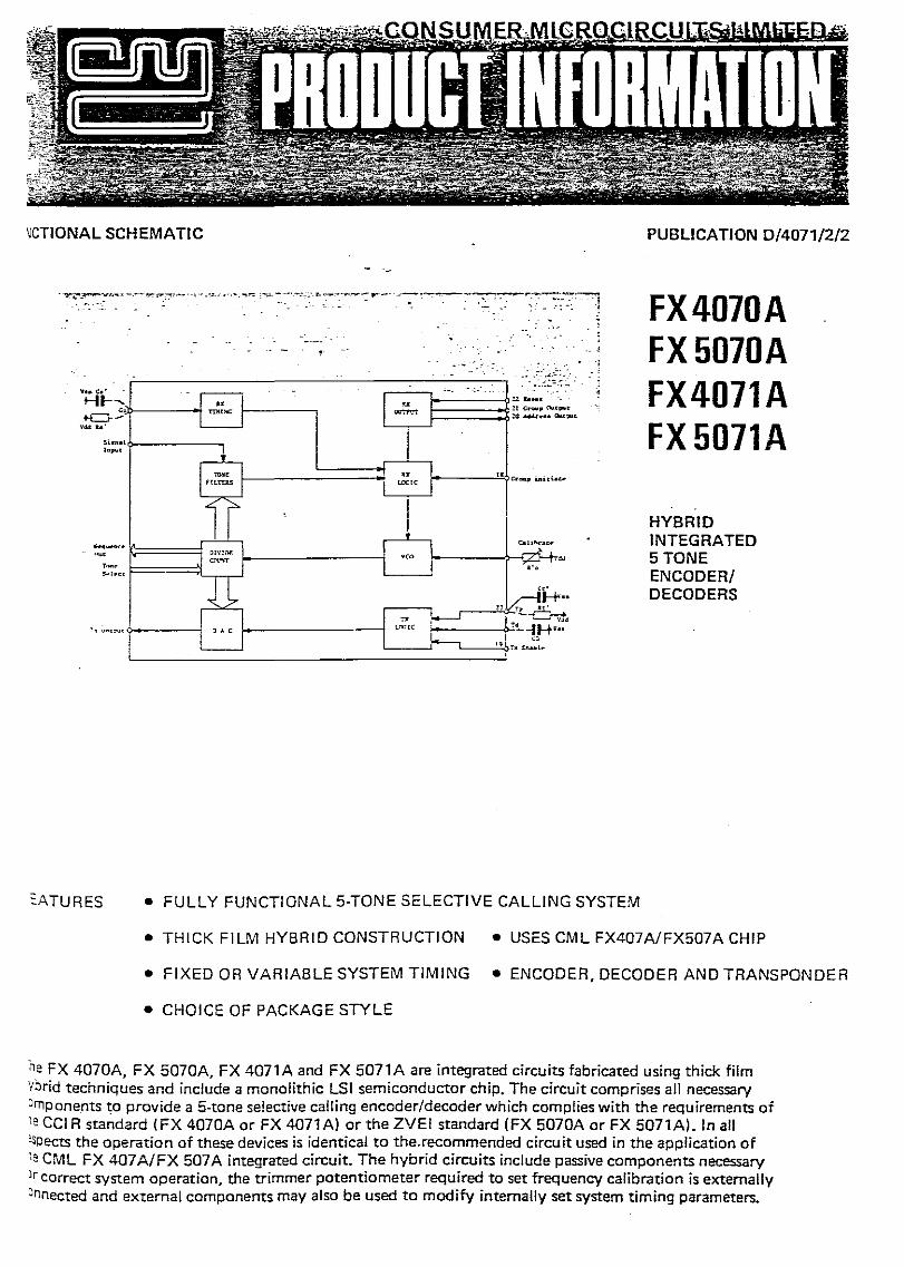
~CTIONAL SCHEMATIC PUBLICATION D/4071/2/2
.. J
.-..;
HYBRIDINTEGRATED5 TONEENCODER/DECODERS
FX4070AFX5070AFX4071AFX5071A
H-..
. - -~ .. ~ ....-- '-. .'
.~
u lllb__
I U ~t Cr<»op <;!ut. mn~ r ~ :C-..U_
,1_, l Iu "fU.tu.S r 'I t,DC1C I Cr_ i...itia
I ,
.! ~lnllol'l I I l:o.li";.n..
1 =~ r I,,"
I "'I·~
1T I~"r l-J
!l T!.. U·
~
", " t.."l;tC . -JH'! ~ ", !, r. ~I..,
-~-"""--::''''''--'',
Si.....,.."".
::ATURES • FULLY FUNCTIONAL 5-TONE SELECTIVE CALLING SYSTEM
• THICK FILM HYBRID CONSTRUCTION • USES CML FX407A/FX507A CHIP
• FIXED OR VARIABLE SYSTEM TIMING • ENCODER, DECODER AND TRANSPONDER
• CHOICE OF PACKAGE STYLE
he FX 4070A, FX 5070A, FX 4071A and FX 5071A are integrated circuits fabricated using thick film'Ibrid techniques and include a monolithic LSl semiconductor chip. The circuit comprises all necessaryJrnponents to provide a 5-tone selective calling encoder/decoder which complies with the requirements ofle CCI R standard (FX 4070A or FX 4071 A) or the ZVEI standard (FX 5070A or FX 5071Al. In all'sPects the operation of these devices is identical to the. recommended circuit used in the application ofle CML FX 407A/FX 507A integrated circuit. The hybrid circuits include passive components necessarylr correct system operation, the trimmer potentiometer required to set frequency calibration is externallyJnnected and external components may also be used to modify internally set system timing parameters.

CIRCUIT DIAGRAM INTERNAl CIRCUIT QIAGRAH Of HYBRIDS••• -j
-. - - ,-, ·'71
• _._ ~ _....... :::: I
.
:IS 24 23 22
,T
-•o
DIGIT SEauENCE ()JTPUTS," _- - _-. I
c_,a
'" ,.
VOO
-1-- ,_vss TX SIG GATE TX TONE RESETGFlP ADO ne GRP
Off' liP PER 100 DELAY PERIOD OJP OiP lIP
HYBRID COMPONENT LIST (This information can be read in conjunction with Production Informationon FX 407A)
RESISTORS CAPACITORS
CIRCUIT DIAGRAM VALUE TOLERANCE CIRCUIT DIAGRAM VALUE TC TOLERANCEREF. REF.
Rl lOOK 5% Cl O.022/Lf X7R 10%R2 lOOK 5% C2A=C2B 470pf X7R 10%R3 22K 5% C3A=C3B O.Ol/Lf X7R 10%R'O lOOK 5% C4 0.22/Lf X7R 10%R'in 330K 10% C5 O.01/Lf X7R 20%RD 680K 10% C6 68pf NPO 5%RS(FX4070AlFX4071 A) 1.22M 2% C'O O.Ol/Lf NPO 5%RS(FX5070AlFX5071A) 857K 2% C'in O.Ol/Lf X7R 20%RT 355K 2% Cs 0.22/Lf X7R 20%Rl 600n 10%R'b 330K 10%
CALIBRATION PROCEDURE
Conditions: VDD = 12.5V, TA = 200 ± 50, no input signals.
1) Programme code 6XXXX(FX4070A/FX4071A) or 5XXXX(FX5070AlFX5071A), where 'X' is anyconvenient digit.
2) Apply VDD. Wait several seconds, then connect a shorting link between pins 23 and VSS.
3) Press the TX Enable button and read the frequency at the TX output. The signal is a continuous tone.
4) Adjust the R' 0 calibration potentiorneter until the frequency is exactly 1541 Hz (FX4070AlFX4071 A)or 1530Hz (FX5070A/FX5071AI.
5) Remove the shorting link between pins 23 and VSS. Calibration is now completed for all channels forboth RX and TX.
2

EXTERNAL COMPONENT CONNECTIONS
1. The address and group outputs are open drain MOS transistors. This allows the outputs to be linked togive a wire - OR if required. Load resistors (10Kn nom.) are required for these outputs from pin 20and pin 21 to -Ve supply.
2. A 22 Kn trimmer potentiometer with a temperature coefficient <100ppm must be connected from R'0to -Ve supply (pin 32). This is used to calibrate frequency as described above.
3. The Output Reset input has an on-chip 1Mn (nominal) resistor to VDD and a 3Kn M.O.S. transistor toVSS which is disabled when the outputs are activated. With this input held at VSS the outputs will tumon at power-up. To reset the outputs and ta.en.sure they are off at power-up the pin must bemomentarily taken to VDD. An automatic time-out commencing from when the outputs are activatedis provided with a resistor in parallel with a capacitor between pins 22 and 32. The interval Ton "'0.65RC seconds, and should be longerthan one tone period.
4. A capacitor (CT) must be provided between pin 23 and the positive supply (VSS) to set the transmittedtone period.
The period is given by:Tp = 0.355K CT seconds.
where CT is measured in p-FK = 0.6 ± 0.03 typ. (a constant of the monolithic chip)
For CCI R tone period = 100 mS (FX4070A or FX4071A) then CT = O.4htFFor ZVEI tone period = 70 mS (FX5070A or FX5071A) then CT = 0.33p-F
5. Optionally:
i) A capacitor (CD) can be connected between the TX Delay pin and the positive supply (VSS) toprovide a delay prior to the start of transmission.
TX delay period = 0.68K CD seconds *
ii) The RX gate period (internally set to 1.75 Tp) can be varied by external components connected inparallel to RS and CS.
RX gate period = K RS' CS' seconds ** where K = 0.65 ± 0.033 typ. RS' and CS' are resultant values of internal and external components,
CD and CS' are measured in p-FRS' is measured in Megohms
PACKAGE DETAILS
,. 1'1l......u
11 vc
u Si
1lI 0"0
"'JOof=
u "
~'~'""'E" ;.".--, ,-. .r_, ~'-..':':l.'C't "
".. 0 .Q
_. i",,-'" ,:
SI lJ
s:e \4
SJ "
"8'"In ~ "'f'>'t.~ '."'1
, "" qn~~._
17 qSlco..L l~"'"
_, ~UQn~,~:, '"" :!C.Ar ~nl""Z4 lOO ~l.
II ~~.l""
n .u.... ,.....,.,..,..,.
~ ".1 I~
n "
" "
u "
_._.
3

FX 4070A and FX 5070A PACKAGE
'fl'CNII1lUtG~ATUII' JlAJIIIOI: ~ t1t ..-entllU4.n-IlATU". IUJltQI.: ..-c.....-c
A
•eD
•FDHI,Kl..N
~ ........t.m .cz..,. "0_31 ...1.01 G.2li1.1 .,o.o:z 0.11G.l 2JO-q 10.'0.1 2.M0.4 10.00.4 10.00.4 10.0O.DIlI 2.,.II.' 2%.'
"
.,~ ~. ,- .... -T. ,., •... - .".-.•. ~_. -
••~---- •--=-'----''''-''-.-'--;.'I I; ,! li!iI!! PUll!!!!!!!!!! lid)) '-' c
f-l,.f I) ,
H
*,.
III-t'1
I.---~.'"FX 4071A and FX 5071A PACKAGE
WO"ICJNGT!M""ATUI'II! II..tJ<tG£: .2lr'CtIt -e:ST'OfIAGE'TEM~AruRE "AHoG£: ...-c .-c
A
•eD
•FGHI
_m~
1.71 •U. 3Da.z ..,om 0..21.1.5 311.1o.az ILIt'-, '-B4,.... usG.' zt.t
eA li!- ,
i D
T --'---Tt
•
I-----L
-LI I_H __
4
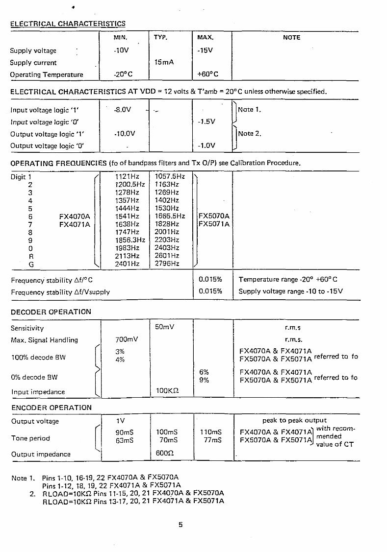
ELECTRICAL CHARACTERISTICS
MIN. TYP. MAl<. NOTE
Supply voltage -10V -15V
Supply current 15mA
Operating Temperature _20°C +60°C
ELECTRICAL CHARACTERISTICS AT VDD = 12 volts & T'amb = 20°C unless otherwise specified.
Input voltage logic '1' -8.0V --' Note 1.
Input voltage logic '0' -1.5V
Output voltage logic '1' -10.0V Note 2.
Output voltage logic '0' -1.0V
OPERATING FREQUENCIES (fo of bandpass filters and Tx O/P) see Calibration Procedure.
Digit 1 1121 Hz 1057.5Hz2 1200.5Hz 1163Hz3 1278Hz 1269Hz4 1357Hz 1402Hz5 1444Hz 1530Hz6 FX4070A 1541Hz 1665.5Hz FX5070A7 FX4071A 1638Hz 1828Hz FX5071A8 1747Hz 2001 Hz9 1856.3Hz 2203Hz0 1983Hz 2403HzR 2113Hz 2601HzG " 2401Hz 2796Hz
Frequency stability 6.f/o C 0.015% Temperature range _20° +60° C
Frequency stability 6.f/Vsupply 0.015% Supply voltage range ·10 to -15V
DECODER OPERATION
Sensitivity 50mV r.m.s
Max. Signal Handling 700mV r.m.s.
3% FX4070A & FX4071A100% decode SW 4°' FX5070A & FX5071A referred to fo,0
> 6% FX4070A & FX4071A0% decode SW 9% FX5070A & FX5071A referred to fa
Input impedance 100KQ
ENCODER OPERATION
Output voltage 1V peak to peak output
[ 90mS lOOmS nOmS FX4070A & FX4071~ with recom-one period 63mS 70mS 77mS FX5070A & FX5071A mended
value of CT
utput impedance 600Q
T
o
Note 1. Pins 1-10,16-19,22 FX4070A & FX5070APins 1-12, 18, 19,22 FX4071A & FX5071A
2. RLOAD=10KQ Pins 11-15,20,21 FX40?OA & FX5070ARLOAD=lOKQ Pins 13-17, 20, 21 FX4071A & FX5071A
5

CODE PROGRAMMING
Programming is achieved by links between the sequence outputs and the digit select inputs. The repeat code(R) is substituted for consecutive identical digits, e.g. 39999 is coded 39R9R. Should the fifth digit becommon to any other digit it must be linked via a diode as shown.
Shortened codes are achieved by linking SS directly to the last digit.
EXAMPLES OF CODING
SEQUENCE OUTPUTS Sl S2 S3 S4 SS Sl S2 S3 S4 S5 Sl S2 S3 S4 S5 Sl S2 S3 S4 S5
tL LLt -t t-L~ L Lt t-tJ Lt • IPROGRAMMING LINKS I
TDIGIT INPUTS 2 o 9 6 4 2 1 R 0 1 5 6 9 3 6 5
PROGRAMMED2 0 2 1 1 0 SADDRESS 9 6 4 1 1 6 9 6 3 6 5
CIRCUIT ARRANGEMENTGROUP CALLING
INPur
COOES
- ---
2. f---SIt>"L FX 401CA I FX SQ7QAINPUT FX4071AI FXS071 A
" r--"
L~vcc
6,.'0Fxt05 9
T ....ltt~
i FX la 5 TUNED TO "Go TONEl
ADDRESS alP
GROUP CIP
','~ IPULSE: INTO PIN 161
. ,,Yl .-
'0' '-----.J .
[
"G"TCNE AECEI'o'EQ ]WAve~OR'" AT PIN 9
OF n:1QS
When an input code contains a 'G' tone, the FX105 switches ON and the 1->0 edge is coupled to the GroupInitiate input (pin 18) of the hybrid. This causes the hybrid to change from the Address code programmed,to an internal Group programme for the remaining digits of the input code. If the Group code is correctlycompleted, the Group output of the hybrid switches ON. The Group Initiate is effective only if the correctfirst two digits of the Address code have been received. The Group Initiate input is disabled during transmitmode, a Group call is transmitted by encoding the 'G' tone via the Digit Select inputs.
EXAMPLES OF GROUP CALLING
INPUT CODE ACTIVATES RECEIVERS CODED: GROUPS OF: I OIP SWITCHED
25784 25784 only 1 ADDRESS
2578G 25780 to 25789 10 GROUP
257GR 25700 to 25799 • 100 GROUP
25GRG 25000 to 25999 1000 GROUP
...CML does not assume any responSibIlity for the use of any CircUItry deSCribed. No CirCUIt patent licencesare implied and CML reserves the right at any time without notice to change said circuitry.

PRODUCT INFORMATION PUBLICATION 0/2030/1MARCH 1983
FX2030CFX2030Z
LOW POWERSELECTIVE
CALLINGENCODER!DECODERHYBRID
T4~1.
T.... n...o<; -ouTJ'ur_l' "'l!"'<1IJt"
21. AlIOItES,>
~"
"I.i I I
(~ Af,LU/.....O-,(, ,- l%caO!'lt
-~ -0(.(I'~ocn
="
{t ,~
"~
AOEWH5IP'<COOC:.', m:::;oQE..t<,I'U~ll
",
[v-,
I,~
r~Irl
1~~,
•-" a'45
, ('-TOl'oIe" ,,--'<Caeelt
~(FxSQll~..
I
"'T1!: ./!iO .. 1O. T.t..
ClOr·lll'"'lT~
TIUoNS_ S~l..t'T
RGURE 1 INTERNAL BLOCK DIAGRAM
FEATURES
• LOW POWER CONSUMPTION
• SMALL PHYSICAL SIZE
• COMPLETE ENCODER/DECODERrrRANSPONDER
• CHOICE OF CCIR OR ZVEI TONE-SETS
• INCLUDES ALERT SLEEP GENERATOR
• INCLUDES GROUP CALL DECODING
• AUDIO SWITCHING
• FEW EXTERNAL COMPONENTS
• SIMPLE INTERFACING
• DATA DECODING
DESCRIPTION DECODER
The FX2030 is a complete selective calling encoder/decoder for 5-tone sequential systems. It offers theadvantages of small size. Iow power consumption,simple interfacing and high performance.
The thick film hybrid combines LSI CMOS chips withdiscrete resistors, capacitors and diodes to minimisethe number of external components required. TheFX2030C is based on the CCI R signalling frequenciesand the FX2030Z is tuned to the ZVEI tone-set
A typical sequence of operation is illustrated in Figure2. The FX2030 decodes a correct selective call andautomatically transponds an' acknowledgement inreply. The hybrid will then switch the Mute output highand generate an alert call to warn of an incomingmessage. Finally the incoming speech signals areswitched through to the output

....._- ..-.~::'rlll;IIIII~1
.- u ._ ''''L --.- ..,." , 'U.... U ...... ' "" ..._.. ,.,.,.,,,~,,.
lIJ'i;:;r -'
FIGURE 2 TYPICAL TRANSPONDER SEQUENCE
ENCODER
The encodersection of the FX2030 is enabled either inresponse to a transmit instruction (Tx) or for automatictranspond (Tp) as illustrated in Figure 2.
EXTERNAL COMPONENTSTo provide a selcall encoder/decoder function theFX2030 requires a few external components as shownin Figure 3.
560kHz Oscillator.
The receiver tone channels, encoderoutput frequenciesand alert patterns together with system timing func·tions are derived from the 560kHz reference. A lowcost ceramic resonator can be directly driven by thecircuit together with a trimmer capacitor to adjust thefrequency as shown. Pin wiring should be kept short.
...-.. ............<l' '".li..u _
FIGURE 3 EXTERNAL COMPONENTS
The 560kHz can be measured by monitoring Pin 14and adjusting the logic level square wave to 23.333kHz.Monitoring Pin 14avoidsdirectly loading the oscillatorwith a frequency counter. All necessary calibration isnow complete.For some applications the small frequency drifts associated with temperature and ageing effects may beunacceptable. In this case a crystal derived clock canbe injected at Pin 2. Under no circumstances shouldpower be applied to the device with no clock presentThis would cause the dynamic logic to malfunction andcould damage the deVice.
Alert Reset
Adding a capacitor to the Alert Reset input (betweenpins 9 and 41) provides an automatic time out of alertsignals. A N/O switch to VDD can be used for manualreset
PIN DESIGNATIONS
Pin1. Osc.l2. Osc. 23. Not connected4. VSS (negative supply)5. Not connected6. Power on reset7. Not connected8. Alert/Audio output9. Alert reset input
10. Data change output11. Data change input12. Transpond select input13. Alert bleep logic output14. 23.333kHz monitor output15. AO memory address output16. A1 memory address output17. A2 memory address output18. A4 memory address output19. Auto repeat input20. Tone output21. Relay output22. DpO(2) memory data input23. DpO(1} memory data input24. Dpl memory data input25. Dp2 memory data input26. Dp3 memory data input27. Transmit enable input28. A3 memory address output29. Mute output30. Mute reset & P.T.L input31. Group digit select input32. Oata flag output33. DjO data jam input34. Djl data jam input35. Dj2 data jam input36. Oj3 data jam input37. Q3 tone data output38. Q2 tone data output39. Ql tone data output40. 00 tone data output41. VOD (positive supply)42. Signal input
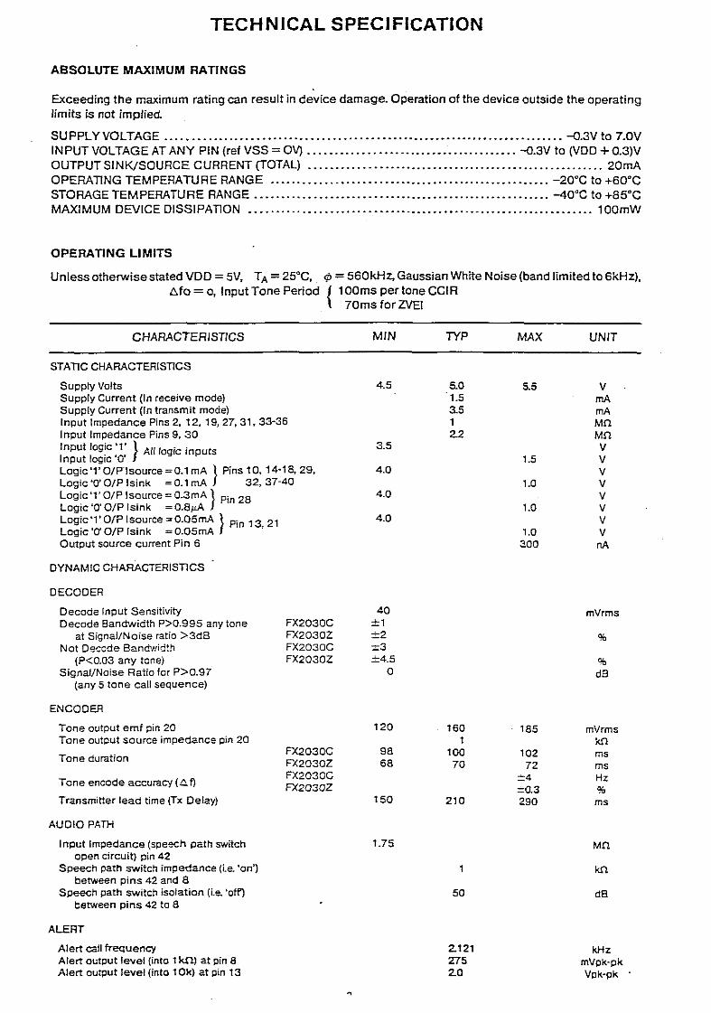
TECHNICAL SPECIFICATION
ABSOLUTE MAXIMUM RATINGS
Exceeding the maximum rating can result in device damage. Operation of the device outside the operatinglimits is not implied
SUPPLY VOLTAGE ....•..•......•.••••.•.•..••.•...•••.•••••.••...••••••••••••..•••••••••••• -<J.3V to 7.0VINPUT VOLTAGE AT ANY PIN (ref VSS = OV) .•..•.•...•..••.•.••.•••••••....•••.••. -<J.3V to (VDD + O.3)VOUTPUT SINK/SOURCE CURRENT (TOTAL) .•....•.....•••.•.•...••••••.•...••.•...•......•...•... 20mAOPERATING TEMPERATURE RANGE •.••....•....•.•...••...•••..••••••.•..••.••••••••.. -20'C to +60'CSTORAGE TEMPERATURE RANGE •.•..•....••••.•.••.•.••.•...•••••.••...••...•••.•...•. -40'C to +85'CMAXIMUM DEVICE DiSSiPATiON .••.......•.••....•...••.••...•••••.••••.••..••••.....•.•..•.... 100mW
OPERATING LIMITS
Unless otherwise stated VDD = 5V, TA = 25°C, </J= 560kHz, Gaussian White Noise (band limited to 6kHz),~fo= 0, Input Tone Period { 1OOms per tone CCIR
70ms for ZVEI
CHARACTERISTICS MIN TVP MAX UNIT
STATIC CHARACTERISTICS
Supply Volts 4.5 5.0 5.5 VSupply Current (In receive mode) 1.5 mASupply Current (In transmit mode) 3.5 mAInput Impedance Pins 2. 12, 19,27,31,33'36 1 MnInput Impedance Pins 9. 30 2.2 MnInput logic '1' } Alllogie inputs 3.5 VInput logic '0' 1.5 Vlogic'l'O/Plsource=O.lmA } Pins 10,14,18, 29, 4.0 Vlogic '0' alP Isink = 0.1 mA 32, 37-40 1.0 Vl09iC'l'O/Plsource=0.3mA} Pin 28 4.0 Vlogic '0' alP Isink = 0.8j<A 1.0 Vl09iC'l'O/Plsource=0.05mA} Pin 1321 4.0 Vlogic '0' alP Isink = 0.05mA ' 1.0 VOutput source current Pin 6 300 nA
DYNAMIC CHARACTERISTICS
DECODER
oeeode Input Sensitivity 40 mVrmsDecode Bandwidth P>0.995 any tone FX2030C ±1
at Signal/Noise ratio >3dB FX2030Z ±2 %Not Decode Bandwid':h FX2030C =3
(P<0.03 any tone) FX2030Z :::4.5 %Signal/Noise Ratio for P>0.97 0 dB
(any 5 tone call sequence)
ENCODER
Tone output emf pin 20 120 160 185 mVrmsTone output source impedance pin 20 1 kn
Tone durationFX2030C 98 100 102 msFX2030Z 68 70 72 ms
Tone encode accuracy (At)FX2030C :::4 HzFX2030Z =0.3 %
Transmitter lead time (Tx Delay) 150 210 290 ms
AUDIO PATH
Input Impedance (speech path switch 1.75 Mnopen circuit) pin 42
Speech path switch impedance (Le. 'on') knbetween pins 42 and 8
Speech path switch isolation (i.e. 'off) 50 dBbetween pins 42 to a
ALERT
Alert call frequency 2.121 kHzAlert output level (into 1kn) at pin 8 275 mVpk-pkAlert output level (into 10k) at pin 13 2.0 Vpk·pk

MIN lYP MAX UNIT
Alert time out using external capacitor C 1.57C 2.1C 2.63C sin p.F on pin 9
Leakage current of capacitor C 0.7 pP.Recommended range of external capacitor C 0.33 4.7 p.FInternal pull-up resistor pin 9 2-09 2-2 2-31 Ml1Swilchover time from Alert to incoming.
speech at pin 8 0.6 s
TIMINGS
Osc. 2 input pulse width (pin 2) 750 893 1000 ns(using external clock)
Power On Reset (pin 6) input pulse width 2 msAlert Reset (pin 9) input pulse width 10 J1SData Change input (pin 11) pulse width 100 J1STransmit Enable (pin 27) input pulse width 100 J1STransmit Enable pulse rise time 10 J1SMute Reset & P.T.L (pin 30) input pulse width 90 J1S
SIGNALLING FREQUENCIES (in Hertz)
Tone o 1 2 3 4 5 6 7 8 9 A B C D E
FX2030CFX2030Z
1981 112411971275135814461540 1640174718602400 9302247 991 21102400106011601270140015301670 1830200022002800 810 970 8862600
Table 2 shows the response of the FX2030 under various input conditions.
TABLE 2TRANSMITTED TRANSPOND TRANSPOND ALERT ALERT AUDIO
TONES SELECT OUTPUT OUTPUT AUTO SWITCH(Note 1) {Note 2) (Note 3) TIME OUT (Note 4) COMMENTS
12345 1 Yes Address Yes On Address call.call Transpond selected.
12345 0 No Address No Not Address call No auto time-outcall applicable Transpcnd not selected.
1234Aor X No Group Yes On Group call or all-callAEAEA call Transpond automatically inhibited.
12345C No Address Yes On Address call.call Reverses Transpond selection.
12345C 0 Yes Address Yes On Address callcall Reverses Transpond selection.
1234586789 Yes Second No Not Addressed data (6789).address/data applicable No auto time out
1234A8 X No Second No Not Group call using second address.address/data applicable Transpand automatically inhibited.
123450 1 Yes None Not Off 'silent interrogate'/mute and resetapplicable Transpond if programmed.
AEAEAO X No None Not Off Mute and reset all receivers.applicable Transpand automatically inhibited
12345CB No Second No Not Second address calladdress/data applicable Reverses transpand selection
12345CO 1 No None Not Off Individual mute & resetapplicable Reverses transpond selection.
123456 X No None Not Off Incorrect address withapplicable too many digits.
Notes: 1) The address code is 12345. A is group tone, E is repeat tone, S. C and 0 are address suffix tones.
2) Indicates input logic state. X = don't care.
3) Refer to Fig. 5 for alert patterns and timings.
4} Defines condition of audio switch after transpond and alert sequences are completed. 'Not applicable' ariseswhere alert does not automatically time out and must be manually reset

DESIGN INFORMATION
Pin Descriptions
OSC. 1 - Output of a CMOS inverter. Can be used inconjunction with the Osc. 2 input to form the activeelement of a ceramic resonator circuit Passive components are included on the hybrid to complete theoscillator circuit
OSC. 2 - Input of a CMOS inverter. Alternatively a logiclevel 560kHz square wave can be injected at this pinwith Osc. 1 left open circuit.
VSS - Negative supply input.
POWER ON RESET - provides·a positive going pulsewhen power is applied to the hybrid The pulse can beused to automatically initialise external circuits butmust notbe excessively 10aded.The powersupply mustrise to 90% of its final value within 2ms to ensureadequate function. Alternatively an external logic '1'pulse from a low' impedance source can be appliedafter the power supply has stabilised
ALERT/AUDIO OUTPUT - linear output pin. The logic'level alert patterns are output at this pin via an im-.pedance of approximately 15kohms. The transmissiongate between the Signal input and Alert/Audio outputIs disabied when alert patterns are being generated.
When the hybrid is unmuted the analogue signals at theSignal input are available at the Alert/Audio output
ALERT RESET INPUT -Includes internal pull-up resistor. The input has a schmitt 'trigger characteristic topermit the use of siow rising voltages for automatic timeout applications. A discharge transistor normally holdsthe pin close to the negative supply and is disabled forauto time out The alert pattern is reset when the inputvoltage exceeds the schmitt trigger upper Iimit(typically0.66 VDD volts).
A switch connecting to the positive supply can be usedlor manual reset
DATA CHANGE OUTPUT - CMOS logic output. A logic1 pulse is output each time the tone decoder detects achange of tone. Normally connected to:
DATA CHANGE INPUT -logic input. A logic 1 inputpulse causes the address decoder to compare the tonecode with the data held in the external address PROM.
TRANSPOND SELECTINPUT -logic input with pull-upresistor. A logic 1 oropen circuit will cause the FX2030to automatically transpond a reply aftera selective callis decoded, and a logic 0 will inhibit this feature.Address suffix tone C inverts this selection and groupcalls. inhibit transpending.
ALERT SLEEP OUTPUT - CMOS logic output.The alertpatterns are available at this pin from a source impedance of typically 5k ohms. In the quiescent state the
output is at VSS.
5
23.333 kHz MONITOR OUTPUT - CMOS logic output.This pin outputs a square wave frequency of 23.333kHzwhen the input clock is 560kHL Most applicationsrequire a calibration tolerance of ±0.1 %.
AO, A1, A2, A4 MEMORYADDRESS OUTPUTS - CMOSlogic outputs used to address the external memory.
AUTO REPEATINPUT- logic inputwith pull-up resistor.
An open circuit or logic 1 enables the encoder autorepeat circuitry. This detects when the repeat frequency is required in an encode sequence.
Repeateraccess applications may require a continuoustone of two or more tone period durations. This can beencoded by disabling the auto repeat feature with alogic O. The memory address outputs increment asnormal after each tone period.
TONE OUTPUT -linearoutputThe output is held at VSSin the quiescent state.
The ac. tone output signals are generated about amean de. level of typically 0.25 volts.
RELAY OUTPUT - logic output This pin outputs a logic1 dUring a transmit sequence via a typical impedanceof '15k ohms.
OPO (2), OPO (1), DP1, DP2, DP3 MEMORY DATAINPUTS -logic inputs. The 4 bit selcall address codesare input to the hybrid by these pins. The least significant bits are fed separately to the tone encoder OPO (2)and address encoder chip DPO (1). This allows theencoder to be programmed to the repeat frequency(code El if required without causing shut-down of thesystem.
TRANSMIT ENABLE INPUT - applying a logic 1 levelpulse atthis pin acts as a transmit enable request Theinternal components couple a pulse through to theaddress encoder.
A3 MEMORYADDRESS OUTPUT - gives aCMOS logic1 output level when a transmit enabie request isaccepted. The quiescent state is a logic 0 estabiishedby a 1M ohm pull-down resistor.
MUTE OUTPUT - CMOS logic output The mute outputis set to logic 1 at the start of an alert output sequencefollowing receipt ofa selcall It is also forced high whenthe Mute Reset and P.T.L input is activated and resetson the falling edge of the input pulse. Reset of the Muteoutput results when suffix 0 is included in an incomingaddress sequence or when a second address/dataalert is reset at the Alert Reset input
MUTE RESET AND PUSH TO LISTEN INPUT -logicinput with pull down resistor. A logic 1 at the inputactivates the Muteoutput (P.T.L feature) and resets analert output sequence. The negative going input edgeresets the Mute output
GROUP DIGIT SELECT INPUT - logic input with onchip pull-down resistor. The address decoder is programmed to recognise tone A as the group digit by alogic Q or open circuit at this pin. A logic 1 programmestone 0 as the group tone_

scanned by the decoder. These are tuned to detectthetone digits 0 to 9, repeat tone, group tone and threeinstruction tones. The divide/count outputs are furtherprocessed to optimise the performance of the decoder.
The tone data is compared by the address decoderchip with the data stored in an external memory. If anincorrect sequence is detected the decoder abortsand remains in standby until the end of the lonesequence. The decoder includes circuitry to identifywhen the repeat frequency is expected in an addresssequence. It automatically programmes repeat in placeof the code digit held in the address memory.
Group Calling.
Completely flexible group call decoding is provided bythe FX2030, without constraints on the calling structure. The examples show Tone A representing thegroup call frequency and E being a repeat of theprevious tone digit:
If a group tone is included as part of a correct incomingsequence the decoder sets an internal latch. At theend of the sequence the state of the latch is inspectedand transponder operation will be inhibited for groupcalls. This avoids the situation where multiple receiversare simultaneously keyed.
DATA FLAG OUTPUT - CMOS logic output When address suffix B is decoded the Data Flag outputs a logic1 and resets back to a logic 0 at the end of the tonesequence.
DiO, Djl, Dj2, Dj3 DATA JAM INPUTS. These pinsconnect directly to the tone data inputs of the addressdecoder, and 1M ohm resistors feed from the outputsof the tone decoder. Normal operation of the devicerequires these pins to be open circuited. Should it berequired, for example, to abort address decoding datacode F can be forced on these pins from low impedancesources (max. 1Ok ohms). A pulse at the Data Changeinput strobes the data into the device.
00, 01, 02, 03 TONE DATA OUTPUTS - CMOS logicoutputs. The current state of the tone decoder isoutput as a 4 bit word.
VDD - positive supply input
SIGNAL INPUT - analogue input The selective callingand speech signals are input to the hybrid at this pin.
DECODER OPERATIONFigure 4 is a flow diagram for the FX2030 decoder.
The tone decoder in the hybrid detects all valid inputtone sequences.
The decoder limits the input signal and processes it inan autocorrelator. The autocorrelator has the effect ofenhancing the coherence of signalling tones whilerejecting random noise. The periodic signal informationis detected and passed to accurate digital divide/countcircuits where fifteen tone bands are simultaneously
Transmitted Tones
1234A12AEAA2345AEAEA
Units Called
12340-1234912000-1299902345-92345
All units
"i£~c.>u.
=""_tCT ~
!'oo 0''i£<;'~><!
~t>£!
"n ....~""Oo(I'(!)<,I'~~'
"'''',HE'0_"",""
,£QUt><t
FIGURE 4 DECODER FLOW DIAGRAM
Alert
An alert outputwill be generated next in the sequence.It is however inhibited for 'Silent Interrogate' (refer toSuffix Tones seciion) as shown by the 'NO' branch inthe flow diagram of Rgure 4.
= ----j'- --..Jf-
---- --.>2 ,'-'
FIGURE 5 ALERT OUTPUT PATTERNS
lilt::: d.1t:::ll ~IYllell elL LiIC r\ICIL/I"\UUIV VULt-'UL \1 ", ..... , , ...
derived from the logic level square wave at Pin 13.Thealert sourCe impedance at Pin 8 is typically 15k ohms.
The 2.121 kHz clock is chopped as shown in Figure 5.An even mark/space alert signals an address call and acontinuous note indicates detection of a group call Asecond address/data call is announced by the distinctive paltern shown.
The alert can be automatically reset by providing acapacitor 'C' on the Alert Reset input Pin 9. Automatictime out is not available for address calls where atranspond is not selected or for second address/datacalls. These must be reset externally by a logic 1 pulseat Pin 9.
An alert will also be cleared by activating either theMute Reset & P.T.L or Transmit Enable inputs.
Audio Squelch
The FX2030 features an audio switch in the signal path.This transmission gate is controlled by the decoderandis automatically turned on atterthe alert has reset Thespeech signals at the Signal input are now available atthe Alert/Audio output
Pin 30 is the Mute Reset & P.T.L Input and as its nameimplies offers two functions. Manual defeat of the muteis provided with a high level at this pin. The 'Push toListen' action is used to check channel occupancy.
The falling edgeofthe input pulse at Pin 30 is detectedand used to mute the receiver.
The remote mute facility is discussed in theSuffixTonessection.
,u>
.p-.......1 ••~.....,.....,...,...
FIGURE 7 DATA AND MUTE OUTPUTTIMINGRELATIONSHIPS
The Data Flag output relationships are detailed inFigure 7 (0 and the Mute and Mute Resetinput in Figure7 (in.
ENCODER OPERATIONTransmit
The hybrid can be used to transmit a code sequence asa calling or identity signal, as illustrated in the flowdiagram of Figure 8.
" ,oL1U S'oOUe-G'o ""'U.T r-,ULL." 1.0.u s.... I;JO-OOOI!..............O:.OU.. __
I-n~
~::f~ ...J1
Figure 6 (i) gives the timing relationships between theTone Data outputs and the Data Change output TheData Change strobe causes the Memory Addressoutputs to increment and the critical Memory Datainput timings are detailed.
Figure 6(ii) shows the timings of the Mute output, AlertSleep Logic output and the Alert/Audio output following receipt of a correct selcal!.
FIGURE 6 MEMORY AND ALERT OUTPUTTIMING RELATIONSHIPS FIGURE 8 ENCODER FLOW DIAGRAM
7

u
11.-0,DATA _Ill
-~_..A._. OIII'...n ~~_--='--='':'__lIX__=--
i--u-;
1/ ZZ IL \'--__'-t
., ---------i1f------_i--r
lIll....l' OU1',."..,~--------..;L
1'....7".5 ca.'" nf_ TUOCn-C'OU .......1C1, ... 4:l11.S
TVICI<I.S "u>o __ 1__JUTl.. or lllloSN"s.. 'Pl~le ,.
n- ,.
,,
~I
.''1
:~-~. ..-. ..l
FIGURE 9 ENCODER OUTPUT WAVEFORMAND SPECTRAL ANALYSIS
FIGURE 10 TRANSMIT ENABLE AND MEMORYTIMING RELATIONSHIPS
A positive pulse at the Transmit Enable input iscoupled to the control chip (FX403) and will be acceptedunless the decoder is processing an incoming selcalLThe FX403 will enable the encoder chip (FX503) andset the Relay and A3 outputs high.
The Relay line is used to switch from the FX503standby clock of 23.333kHz to a 560kHz clock useddUring encoding. This technique is used to reduce theoverall power consumption to a minimum.
The Relay line is also used to start a delay period oftypically 21 Oms. This transmit delay allows time to keythe transmitter in a transceiver before the start of thefirst tone. Additionally the Tone output is set to a d.c.level of approximately 0.25 volts. The tones aregenerat"d about this mean d.c. level and the delayallows conditions to stabilise before encoding starts.
The tone data is read from the memory "and automatically updated as required by the FX2030. Figure 9(I) illustrates the tone waveform generated by thedevice togetherwith the relative levels of the harmonicsof the tone. the harmonic content can be furtherreduced if necessary by the simple filtenng providedby a 0.1 f-1-F capacitor between the Tone output andVSS. This would yield the waveform and spectralresponse shown in Figure 9 (ii).
Each tone in the sequence is generated for an accurately timed period when the hybrid will automaticallyaccess the next memory location. The new data isinspected forthe end oltransmission instruction (codeEl from the memory which causes the Relay and A3outputs to be reset to logic O. The Tone output willrevert to its quiescent level (VSS) and the encoderchipis returned to the low current standby condition.
Transpond
The transpond feature is used to automatically acknowledge correct decoding of a selective call. The replysignal can be decoded by the calling equipment toverify that contact is established
The FX2030 is programmed into transpond mode by alogic 1 or an open circuit at the Transpond Select input
(pin 12). Logic 0 on this pin will inhibit transponderoperation. The encoder sequence is initiated immediately after the end of an incoming call as illustratedin Figure 2 and Figure 8. DUring the sequ"ence bothA4and the Relay outputs will be at Logic 1 and will resetwhen the FX503 is disabled at the end of transmission.Figure 10 (i) gives the timing relationships between apulse at the Transmit Enable input and the A3 andRelay outputs..ln Rgure 10 (iQ the outputs Aa-A2 areshown addressmg memory location N+ 1.This containscode E which flags the end of an encode sequence.
SUFFIX TONESThe function of the FX2030 can be modified by addingextra tones after a selcall sequence. One or more ofthe three instruction tones B, C and D can be added tothe end of a call.
Tone B.
Tone B can be used in a system in one of two ways.
Data messages can be added to selective calls byusing additional tones to represent the data charac·ters. Address and data sections of the call are separatedby address suffix Tone B. The Data Flag output (pin 32)will be set high for data loading when tone B follows avalid address and remains high until the end of thetone sequence. The data is available as four bit words(hexadecimal) at the Tone Data Outputs (pins 37-40).Figure 14 shows the FX2030 interconnected to anFX313 display driver circuit
The suffix Tone B also causes the circuit to generate adifferent second address/data alert output as illustratedin Figure 5. Automatic time-out of the alert is inhibitedand can be reset by either the Transmit Enable or MuteReset & P.T.L inputs. If a selective call is transmittedwith Tone B suffix but no data it can be used as a'second address' facility.
A second address caB could be used when a positiveresponse such as 'contact the base' is required
Tone Bean be used in conjunctionwithC orD but mustalways be transmitted last in the sequence.
MEMORY CODING
E54321
0001 00100011 0100 0101 0110
Memory location (bin) 0001 0010 0011 0100 0101 0110
RxlTp code (hex) 1 2 3 4 5 E
Memory location (bin) 1001 1010 1011 1100 1101 1110
Tx code (hex) 6 7 8 9 9 E
Memory location (bin)
Rx code (hex)
Example (Q Rx code 12345Tx code 12345Tp code 12345
Example (liQ Rx code 12345Tx code 67899Tp code 12345
Memory locat;on (bin) 1001 1010 1011 1100 1101 1110
TxlTp (hex) 6 7 8 9 9 E
The interconnection pattern in (iiQ utilises A3 output. It isused where the receiver code 12345 is automaticallytransponded but a different number 67899 is neededwhen the Transmit Enable button is pressed
(Iv) Should it be required to transmit (using TransmitEnable) the receive code as an identity, but an alternativecode when transponding then interconnection (iv) is used
Example(iQ Rxcode 12345Tx code 67899Tp code 67899
I ne r X2U;;U lulllllS !ne reqUirements 01 5 tone selcallsystems but is also compatible with other sequencelengths. The hybrid is instructed when the sequence iscomplete by code E in the memory as indicated.Therefore ifforexample fourtones are required the fifthlocation would be programmed with code E as shownin example (v). Codes where two successive digits arethe same do not require special programming. Asillustrated in (iQ 67899 is coded as normal but thehybrid substitutes the repeat tone where necessary.
Illustration (Q is the simplest interconnection pattern.The outputs AO. A1 and A2 will provide indenticalreceive (Rx). transmit(Tx) and transpond (Tp) codes. Anexample of the codes held in the memory to give a callnumber 12345 would be:
Memory focation (binary) 001 010 011 100 101 110
RxlTxlTpcode(hexadecimal) 1 2 3 4 5 E
In (iQ the Relay output is used asan input to the memory.To pro9ramme 12345 as the receive code and 67899 fora calling number. the memory would contain:
~--
.,__ ::1
'uu
Tone G.
A call followed by Tone C will reverse the transpondselection programmed at Pin 12.Therefore a responsecan be inhibited from an equipment which normallyreplies or alternatively it can be requested This featuremay be employed in a system where not all equipmentshave the capability of decoding transponded calls.Including Tone C at the end of a transpond sequencewill prevent the possibilty of transponder lock-up. Thiscan occur where a transponded call is decoded anditself causes a further transpond.
Suffix Tone C is redundant for group calls.
Tone D.
Suffix instruction Tone D can be added to a call andresults in two actions. Firstly it will both reset any alertrunning when thecall was received, and inhibit an alertoutput It will also mute the receiver audio by disablingthe audio switch and reset the Mute output
The mute and reset instruction does not affect thetransponder operation of an address call so it forms a'silent interrogate' instruction. Equally the suffix tonecan be applied to an all-call to reset all the receivers ona system.
The external memory contains the address code forthereceiver, together with the transmit and transpondcodes. The address digits are held as four bit (hexadeciman codes in the memory. Six different outputsfrom the hybrid could be used as address lines to thememory.
AO,A1 and A2 outputs increment in a binary count from001 as shown below. These are used as the three leastsignificant digits of the memory address. The A3 outputgoes high only for the time that a transmit instruction(from the P.T.T. button) is being encoded. Similarly A4 isset to logic 1 during a transpond sequence, while theRelay output is high wheneverthe hybrid is transmitting.
The interconnection chosen from the five options shownin Figure 11 will be governed by the requirements of thesystem.
FIGURE 11 MEMORY INTERCONNECTIONOPTIONS
Example (iv) Rx code 12345Tx code 12345Tp code 67899
Memory location Ibln,l: 0001 0010 0011 0100 0101 0110
RxlTx code (hex) 1 2 3 4 5 E
Memory location (bin) 1001 1010 1011 1100 1101 1110
Tp code (hex) 6 7 8 9 9 E
9

•••~
-"} "a: '·'0'0-_... ~.
,. '-'
I, I" J .... ."'\" '-I ..
:::J~.] .c...~n ,--,.,
" ' '''1. '0._1
'-~ ',;'" ..I" " ., '-J
I
~".'t
,..."""..-.,
,......,,,..-.,
- {"- ..- .,~
FIGURE 12 LOW POWER MEMORYFIGURE 14 ADDITIONAL CIRCUITRY TO ADD
LED DISPLAY DRIVER
(v) Connecting the FX2030 to the memory as (v) willgive independent codes for receive, transmit andtranspond The five lines AO to A4 are used to addressthe memory. Four tone sequential codes are illustrated.
Applications requiring minimum possible -power consumption can utilise a fusible link diode matrix and a 416 line decoderwhere space allows. The arrangementshown in Rgure 12 has two independent five tonecodes programmed into the matrix.
Example (v) Rx code 1234Tx code 6789Tp code 4567
Memory location (bin) 00001 00010 00011 00100 00101
Rx code (hex) 2 3 4 E
Memory location (bin) 01001 01010 01011 01100 01101
Tx code (hex) 6 7 8 9 E
Memory location (bin) 10001 10010 10011 10100 10101
Tp code (hex) 4 5 6 7 E
Suitable memory types are fusible link PROM's or U.V.EPROM's in CMOS technology.
APPLICATIONSThe FX2030 is designed to prOVide selcall encode/decode facilities in application where both space andpower consumption are prime considerations. Batterypowered equipments such as hand-held radios providean obvious example. Figure 13 shows the application ofthe FX2030 in a transceiver. The output from thedemodulator is fed to the setcall signal input and theAlert/Audio output is connected to the audio amplifier.The Mute output can be used as an enable control.
A summing amplifiercombines the microphone signalswith the FX2030 Tone output before passing to themodulator.The transmitter section and aerial switch ingcan be controlled by the Relay output combined withthe P.T.T. button.
__• <:OOOT[",rs.,u_1 2 ~ ., ,
ralr" CllQI! .7 • , , • 'U"nJ$l
_~ LOI:.Iofl'- ,ala) -, "" "" " .. 0101 eno OlU -U c:ooc (..u) , , , • • •_'" UlC.&l'Io. (al.) .- 1010 1011 .... nOl 1110 u.u. ,-nil" CQIilC: ("'b") • , • • • • • •
_nA. :•
.,~ .,"lj~:
, ..~
,';"- .-
FU010
~$([~. ,....us., , _.nll)
'" "", ", , ,
'",. , "CI'OIJ.l , "
Dl"lllll
~~,~ lip,.
iiT! ~"
I' ,"1 IS.C.C1.s... rc..
I C(lOO.
'(
I'_'~.I I~o"~,,,~ AElIl ..... f-.~~......LIFI1;;lI L-J ",toU,""
rUsrc;"""l.
lI€L"· l_ur
c~FXlO1Q
, r~.l"""'l!ll:
."~" ~"
..... €1IT1Al,1OI0
./S ~ O\JT..... r1I.T.L.
er",'. !'.L.
IrQ.II).~ L. -_. ..
-~
". T. rl!lurrOl'l
FIGURE 13 APPLICATION IN A RADIOTRANSCEIVER
FIGURE 15 ENCODING A SINGLE STATUS DIGIT

.. .. 4001
U ... bl H "111 O'IIT " "..
;-' &) ~7
" "~
~154'~
.. . - .'-mOlO , , , , , (re:.. :lea _~.n
. _t411~,
"~ " ,~,
"D"Otll,
qon7 "6. CI"Ot21~ I •
I I~"ii .. if"",11""1••(:.D. 1 '.C.O. ~ IcoPt.
t~.
.lU.. OIOO! U'",'" oa sr"'u......._aT COHTr",Ts. S>tOl'lO 4s. TwO l"f!:I.&OrCI><&l.. Ot....'O'CTra5.
JUccor 1214!n/Tp cooe 1 2 1 UllITC" I) (s-.no. n
lCKIaT l..OCAoTlO" (SUo) COal. 0010 Oell. Oloe elOl ouoall COOl! 11'1 1'"2 1'"1 1'4 l"! Fl!
I'IV!OllT u:te&nOlO (SI'" leOl 1010 1011 noo 1101 l11eTUn> =r. 11'1 1'2 Fl l!I' 01' I'"l!:
FIGURE 16 APPLICATION TO PROVIDE TWOVARIABLE TRANSMIT DIGITS
Figure 14 identifies the interconnection required toadd an FX313 display/driver to a system. The LEDc1isplays data characters transmitted selectively to thehybrid.
The circuit shown in Figure 15 details the changesnecessary to provide encoding of a single status digitA high level at the FX2030 data input will be due to theeffect of the pull-up resistor, while a low level is derivedfrom forward biasing the diode.
The memory in this example has a 4-bit output, andmust give a valid logic level at the FX2030 data inputwhen the forward volt drop ofthe diode is included. Thegate decodes the state during transmit when thememory data is F and enables the status switch. TheDpO-Dp3 data inputs will then be coded via the diodesfrom the switch. Thememoryis programmed to decode12345 as an address call number but to encode ineither transmit or transpond a sequence 678998followed by the status digit. Tone B is used in thisinstance to separate the 5-tone code from the statusinformation tone to avoid aliasing selcall codes.
Figure 16 shows an efficient technique of enablingselector switches during a transmit sequence. ThePROM is organised as an 8-bit output with 4 bits usedto carry the hexadecimal tone codes. The 'common'input of each switch is allocated to oneofthe remainingmemoryoutputs and is pulled low at the correct timebyprogramming logic 0 at that output. These are shownas the hexadecimal codes E and 0 programmed intothe Tx/Tp code sequence.
The circuit schematic shown is used to vary the lasttwo digits of a 5 tone code. All receivers on the networkwould have the same first three digits, in this case123XX. Up to 100 receivers could therefore be directlycalled using two selector switches.
The NOR gate shown in Figure 16 illustratesa techniquefor saving power. The FX2030 only requires to inspectthe PROM data during decoding or encoding. Thepower dissipated at other times can be greatly reducedby disabling the memory. The chip enable or select
11
InPU[ IS rnererore conrrOllea oy comolnlng [ne Helayoutput with the Data Change output from the FX2030.The hybrid must always have logic levels applied at itsinputs and these are provided by the pull-up resistorsduring standby.
INTERFACING AND ELECTROMAGNETIC COMPATIBILITYThe FX2030 requires a clock of 560kHz which isinternally converted to logic level square waves. Consideration should therefore be given to possibleinterference problems with RF or IF circuitry caused by560kHz or to its harmonics. Similarly the performanceof the device could be impaired if high levels ofradiated powerwere present near the high impedanceoffered by the Signal input
During the time that the audio is muted the transmissiongate between the input and output is disabled (pins 42and 8). The impedance offered at the output is thereforevery high. When the mute is lifted the hybrid closes thespeech path with an impedance of typically 1k ohm.The changes in the loading effects On circuitry and anypossible interference pick up from high impedancesshould be considered when interfacing the FX2030into a system.
HANDLING PRECAUTIONSThe FX2030 contains CMOS LSI circuits which includeinput protection circuitry. However, precautions shouldbe taken to prevent static discharges which can causedamage.

"
-I •• !--,.
u,
'"unl---
'1.' ., >on
.t=-
• 1 J ,. Z:!
1 I
,,'
,
11 '~
-,11 ",-oa__" __ lr .--.-.,---.-.;I'%'11I-~-\"'''''''-------
FIGURE 17 INTERNAL SCHEMATIC
MECHANICAL
r ' , 'loo0 OJi--,,. t
The hybrid is constructed on ceramic substrates withthe chips and other discrete components added Thechips are individually protected and thewhole assemblyis then coated to provide both mechanical and environmental protection. The package outline is given inFigure 18.
Pin 1 is identified on the package outline of Figure 18and a'" is printed on the top of the product
,'11111111J11111111JII~-4 ~;... •• - Ul_ -+
coClCl
I,---
FIGURE 18 PACKAGE OUTLINE
NOTE:CML does not assume any reponsibilily for the use ofany circuitry described No circuit patent licences areimplied and CML reserves the right at any time withoutnotice to change said circuitry.
--:,;;00 _, "'. . __~ .' ..~__ "_ ~ .!O;...'.-
:983 Consumer Microcircuits Limited 0483/3000

Features
• 15-Tone Selcall Decoder
=Group Call and Data Capability
.. Excellent Noise Performance
• 4 Bit Data Output
.~ Few External Components
Publication 0/003/4 February 1990
• CCIR, ZVEI, EEA, EIA Tone Sets
• J.l Processor Compatible
• High Dynamic Range
• low Power CMOS
• On-Chip Oscillator Useslow-Cost Resonator
FX003QCFX003QZFX003QEFX003QAFX003QZS
HQCj) liP
POWER UPRESET
°9C-,/P
CLOCK ~= +GENERATOR .,
CLOCK OIPZl.J:.:lJkHz
osc. O/P' Fig. 1 Internal Block Diagram
The FX003 is a CMOS QTC (QuadradecimalTone Coding) tone decoder which may beused to decode Selcall tones in accordancewith CCIR, ZVEI, EEA and EIA internationaltone standards.The FX003 detects an input frequency fallingwithin any of the fifteen tone channelsprogrammed on-chip and outputs thehexadecimal tone number in 4-bit binarycode. When a tone is detected, its 4-bit codeis latched at the data outputs and a DataChange is generated. Failure to qualify anytone for a continuous period of 33 ms causesthe output to be set to 'Notone' (16th logicstate) and a Data Change strobe to begenerated.A DATA CHANGE output signals each changein the output code and can be used with theHOLD/ ACKNOWLEDGE input to establish
handshake routines with microprocessors andother data processing logic.A 'Power Up Reset' (PURS) routine ensuresall internal circuitry is correctly reset whenpower is first applied to the device. Following'PURS' the FX003 generates HEX 'E' (NODATA CHANGE) which in turn is followed bya normal decode sequence.The on-chip inverter may be used with aresonator to provide the 560 kHz masterclock for the device, or an external clock maybe used. A divided down buffered 23.33 kHzclock output is also provided for use withother '03 devices and trimming of the560 kHz resonator.The FX003 is available in a number of pincompatible versions, each versionprogrammed in accordance with thefrequencies and bandwidths of a specifiedQTC toneset.

Pin Description(See Figure 2)
Function
D.I.LFX003*
'~:::;,~~:,::.:~~-:~>.~-:c-:",o-_·_""~",,:~,-,,,~,Chip Carrier ",
FXl02K FX202*K(see !vote A)
-QC, az. QE. QA, azs
1 2 23.333 kHz Clock D/P: A 23.333 kHz buffered squarewave logic outputdirectly derived from the oscillator frequency {nominally 560.0 kHzl. Maybe used for auxiliary functions e.g. 560 kHz resonator trimming,externaltiming of received tone periods and for other '03 family products.
2 4 Xtal: Output from on-chip inverter.
3 6 Xtal/Clock: Input to on-chip inverter may be used in conjunction with XtalDIP and 560 kHz resonator or as a buffered input for an external clock(nominally 560.0 kHz).
4 10 5 VSS: Negative supply.
5 8 Hold liP: Active when at VSS. If hold is taken to VSS when the input tonechanges it latches the next data change pulse at logic 1 until the Hold isreturned to VDD. This facilitates Interrupti Handshake routines for microprocessors when used in conjunction with the Data Change DIP. Tie toVDD if not used.
6 9 Power Up Reset A logic 1 level of at least 1 ms duration is required atthis pin to reset internal circuitry on power-up. For slow-rising powersupplies increase the time constant of the components shown accordingly.
7 & 16 1 3 5 1 2 37 8 9 6 710
11 12 11 131415 14 1516 18 18 2020 21 23 2422 23 26 2825 27
8 16
9101112
22
Internally Connected/Open Circuit Should be left open circuit.
Data Change: A pulse is generated at this pin shortly after detection of atone and new data being presented at the Q o - Q, outputs (see Figure 5Timing Diagram).Q'I Data Outputs: A 4-bit word whichQ, is output after a successful decodeQ, and represents the Hex code for theQo decoded tone frequency.
13 19 25 VDD: Positive Supply.
14 24 Signal Input Audio selcall tones are a.c. coupled to this pin via acapacitor. D.e. bias of the internal high gain limiter is set up by connectingthis pin via a resistor to the bias pin.
15 26 Signal Bias: These pins should not be loaded with any other circuitry.
313
93.333 kHz Osc liP }~ FX102K/FX202-K: Interchip connections.93.333 kHz Osc 0 I P. These pins should not be loaded with any external
27 Logic Signal liP. circuitry.17 I Logic Signal O/P FX0Q3·D.I.L: internally connected.
:1.. ~;:~;=and FX202 4 K are sold as a pair, and represent thesame circuit function as the FXtXJ3· D.I.L. deVIce.
•2

EXTERNAL COMPONENT CONNECTIONS
NAL BIAS
!---SIGNAL liPIn
}
OUTPUTS(Hexadecimal Codel
(23 333 kH )zCLOCK OIP 1 'V' 16 •C XTAL 2 15~SIG
XTALlCLOCK 3 14T2M •
--rvDD 0'
.~ IMO HOLD liP4 FX003 13
5 12 Q.oy, PUR 6 11 Q,lOn • 7 Q,10
DATA CHANGE 8 9 Q,STROBE OIP
VD
VS
See Fig. 4
Fig. 2 Dual-In-Line
* QC, az QE. QA, OZS• No connection. Do not tie.D In recommended value for C, Z. E and ZS versions.
2.2n recommended value for the A version.
INTERCONNECTION OF FXl02K AND FX202*KAND EXTERNAL COMPONENTS
XTAL/CLOCK
IIIIIIII__ .J
I 470
FX003*(FX102Kl
INTERNAL INVERTER
~_56J)_kH'_l470 T
IIIIIII ").().-,-/--~
IL_~~~ -.!~'
IM
HOLD lIP
10"
voa (+ VE SUPPLY)D'"
~~GpNU~l"""hr---,
22M
23.333 kHl-
See Fig. 4CHIP CAnRIERS VIEWED FROM ABOVE
LONG PAD (UNDERSIDEJ DENOTES PAD 1.
Fig. 3 Chip Carrier Fig. 4 560 kHz Resonator Circuit
Tone Frequencies If0) in Hz
003QA 003aC 003aE 003QZ 003QZS Output Code aTCIEIA) ICCIR) (EEA) (ZVEI) (ZVEI-S) a, a, a, a o Format
Character
600 1981 1981 2400 2400 0 0 0 0 0741 1124 1124 1060 1060 0 0 0 1 1882 1197 1197 1160 1160 0 0 1 0 2
1023 1275 1275 1270 1270 0 0 1 1 31164 1358 1358 1400 1400 0 1 0 0 41305 1446 1446 1530 1530 0 1 0 1 51446 1540 1540 1670 1670 0 1 1 0 61587 1640 1640 1830 1830 0 1 1 1 71728 1747 1747 2000 2000 1 0 0 0 81869 1860 1860 2200 2200 1 0 J 1 92151 2400 1055 2800 886 1 0 1 0 A2433 930 930 810 810 1 0 1 1 B2010 2247 2247 970 740 1 1 0 0 C2292 991 991 886 680 1 1 0 1 0
459 2110 2110 2600 970 1 1 1 0 ENOTONE NOTONE NOTONE NOTONE NOTONE 1 1 1 1 F
3

-55°C to 125°C
- 3Q°C to +85°C
-0.3V to 7.0V-0.3V to (VDD + 0.3Vl20mA
}}Storage temperature:
SpecificationAbsolute Maximum RatingsExceeding the maximum rating can result in device damage. Operation of the device outside the operating limits isnot implied.Supply voltageInput voltage at any pin (ref VSS = OV)Output sink/source current (total)Operating temperature range: FXOO3*
FXl02K/FX202K*FXOO3*FX102KI FX202*
Maximum device dissipation*QC,OZ,QE,OA,OZS
l00mW
Operating LimitsVDD = 5V, TA = 25°C, c/J = 560kHz,M~ = O.All characteristics measured using the standard test circuit with the following test parameters, and is valid for alltones unless otherwise stated:-
Characteristic See Note Min Typ Max Unit
Static CharacteristicsSupply voltage (VSS = QVlSupply current
3.3 5.0500
5.5 v/lA
Logic '1' output I source = 0.1 mALogic '0' output I sink = 0.1 mALogic '1' input LevelLogic '0' input level
1122
4.5
3.50.5
1.5
vVVV
Dynamic CharacteristicsSignal input rangeDecode Bandwidth (P:;'0.9951
OAQCQEOZ/OZS
344a4b4c4d
0.1
20112
VDD Vpk-pk
±Hz±%±%±%
Not-decode bandwidth (P';;; 0.031OAQCQEOZ/OZS
5555
6033
4.5
±Hz::::0/0±o/a±%
OAQCQEOZ/OZS
Noise response rate Ihours per F- F- Fsingle character responsewith no input tonel.
Decode response time:Notone to tone (F- F)Tone to notone. Tt (F- FlMin. intertone gap for 'F'
6 0.15 I;our6 40.0 Hour6 40.0 Hour6 1.0 Hour
7 20 25 Tp ms7 33 53 ms8 15 28 ms
Nm~ ~
1. Relates to output pins 1, B, 9-12. 6.
2. Relates to input pins 5 and 6.
3. A.C. coupled, sine/squarewave. Z
4. With minimum tone period (Tpl specifiedfor toneset. P = decode probability: B.
(a), (c) SNR 3dS(b), (d) SNR OdS
All conditions of input SNR and amplitude withmaximum Tp specified for toneset.Gaussian input noise, bandwidth 6kHz, maximumi':!.put level corresponds to I-digit code falsing rate.F = random single character.Delay from change of input (tone applied/removed) tochange at Qo- Q,outputs (see fig. 5).Included in T,. Minimum tone gap requirement for'notone'recognition. Outputs = F after delay.(see fig. 5).
4

DATAZ
T7 •Tt
'-i F ~~T. I--' -- ~j
.
Tp I
*TONE 1 X TONEZ TONEN
>:NOTONE"
I T.I•
DATA
DATA CHANGE
vcc~ ~' ..
~R~···
I :JI;=~~~C=======~=-INPUT .;:t:::OT,:,:C::,N:;~-,-T-CK,- ....)
. I
n.:::::::::=m__Q, __t•
Q 2 :::: T
Q. TI ,I I II I I I I
~I""T:::~-II~~-,T-+I__-,C",A",T,:::A-,t +__~~:'="'__-+ .!!CA"T~A~N~__~
31~~ •T5~ ,
fl=f1=_T•__----'- l...-__--..lirLT
=-----------------i
NOT DRAWN TO SCALE
Fig.5 FXOO3· Timing Diagram (See References) • QC, Q2; QE, QA, azs
T'jpical ?"rfmmar.c~
References:
T, Logic 1, > 2 msT2 >33ms&<50msT2 33 ms fDATA E)T. 20 ms minimum (Tp MAXIMUMIT.O.5ms - 1.0msfDATA CHANGEIT. 1.0 ms fDATA CHANGE PULSE DURA TlON)T7 >50flST. < 120 flS
t Q o - QJ will represent the input frequency presentduring and after PUR (shown as 'F' (Notone) in thisexamplel.
tt After application of HOLD the next Data Change pulsewill stay high until fiOO5 is removed according totiming shown.
5

?3C:{3ge CutHnesThe ceramic dual-in-line package of the FX003is shown in Figure 6 and the chip carrier versionshown in Figure 7. For the D.I.L. package, thepins number counter-clockwise (top view) from 1with reference to a notch as a guidance. Forthe chip carrier package, pins number counterclockwise (viewed from above) from the longpad (pad 1).
Handling rrec3utionsThe FX003 is a CMOS LSI circuit whichincludes input protection. However,precautions should be taken to prevent staticdischarges which can cause damage.
.-:g. 6 F.;{CD3* D.j.!"'. ,~3c/(age ~. 7 r-:""Q'''v !~n""* '/ C'· C . ~ ,rig. r,,"\. J L.f\.; L ....'..:; . i\ /7/.0 arner rDcxage
Inches mm.A 0.80 20.32B 0.59 15.00C 0.77 19.$6o 0.11 2.79E 0.01 0.25F 0.30 7.!i2G 0:70 17.7BH 0.10 254, O.orB OASJ 0.155 3.54
Inche:s mm.A 0.45 11.4B 0.41 10.4C 0.41 10AD 0.45 11AE 0.06 1.5F 0.06 t.5G 0.05 1.3H 0.02 0.051t 0.1 2.54J IDENT
.~'", ~r(0)""'I .. , ,
. ,
nr ~ .r-~ 11 11
1[,,==[~jl, ,
I ro
[,-.
• QC, az. QE. QA, QZS
- -- -
FX003*FX102KFX202*K
16-pin Ceramic D.I.l.28-pad Ceramic Chip Carrier28-pad Ceramic Chip Carrier
* VERSIONSQC : CCIRQZ : ZVEIQE : EEAQA : EIA
QZS : Suppressed ZVEI
Note: FX102K & FX202*K are available in pairs only.
CML does not assume any responsibilitY far the use of any circuitrY described. No circuit' patent licences. ace impliedand CML reserves the right at any time without notice to change the said circuiuy.

PRODUCT INFORMATION PUBLlCATION- D/FX 'OJ-K/1 JANUARY 1912
FX102'KFX202C'14FX202Z-kFX103-KFX313'KFX403-KFX503C-kFX503Z'J(
~..=....~-
q::-..''"~
"-
___ -e--- -.:
n
n'....n.u....u-
-::.."~..-~-
----- ..• __.~._---.-._- _. -- .........---------"~~----~---. --~-- ...., ...,sr-....n-.-~ .-e -.:
I I I
i:1 Jl
FEATURES
* SMALL PHYSICAL SIZE * WIDE TEMPERATURE RANGE
* C SUFFIX DEVICES TUNED TO CCIR TONESET * HE~~TICALLY SEALED PACKAGE
* Z SUFFIX DEVICES TUNED TO ZVEI TONESET * LOW POWER CMOS PROCESS
GENERAL DESCRIPTION
FX003 PRODUCTS PACKAGED IN LEADLESS CHIP CARRIERS.
Products from the FX'03 range are available packaged in leadless chipcarriers. This form of packaging can result in a greatly increased packing density.
The ceramic leadless chip carrier provides a high level of packagehermeticity and wide operating and storage temperature ranges.

DESCRIPTION
The circuit function and electrical specification of leadless chipcarrier products are identical to the dual-in-line product information with thefollowing exceptions:
a) The FX003 tone decoder comprises two discrete Lsr chips whichare each packaged in a chip carrier. Both packages are requiredfor a complete tone decoder, and are available to decode theCCIR or the ZVEr range of signalling tones. The product codesfor a CCIR decoder are an FXI02-K together with an FX202QC-Kand for a ZVEr device are FXI02-K and FX202QZ-K. The interconnection and external components of the -two chip carriersare given in diagram 2.
The supply current taken by the FXI02 and FX202 combined istypically 1200vA at 5 volts supply.
b) All chip carrier products are specified for operation oversupply voltage range 4.5V to 6V.
IN"ITF!C()NNEC':"ro~ O~ FX!02_K AND FX2021C
"'-"10 E-X,ERSAL CO,",PONTII'!"S
2n2
~~~ -11-1,.--,
5-65pF-
VUOhVE SUPPLY)
0
0
}"Q2 D.\TA
0' a<n'P<n'S
FlG.2
~ ---4-VSS('1IE: SUI'I'LY
m:rco- {Tie t.o VDO
if not .requ.1r~d_
CRI? CARlHERS vrooeo FROM ABOVELONG PAD IUSDE:RSr~E:1 D~"IOTES PAD 1.
Leadless chip carriers may be attached by reflow soldering techniques.A typical reflow temperature would be 2100 C and the molten solder tends to alignthe chip carrier over the solder pads on the substrate. The ideal substratematerial is ceramic because it has a coefficient of linear expansion very closelymatched to that of the carrier. Epoxy glass printed circuit boards can be usedbut the unmatched expansion coefficients lead to strain on the solder joints duringcooling.
Care should be taken when handling any C}!OS product to minimise thepossibility of the static electrical discharge into the input pins.
VDD (+VE SUPPLY)
typicalinputcircuit
INPUT o--.......--j
VSS( -VESUPPLY)
During storage the devices should be protected from static charges byoackagin2 in conductive foam or storage in metal trays.

PIN DATA
FX202QC-K I FXlO3-K FX3l3-K FX403-K FX503C-KPAD FXI02-K FX202QZ-K FX503Z-K
1 N/c N/C Data Chng. rl VDD (+) Data Chng.r/p Tone alP
2 Z3.333kHz lip N/c PUR rip DD rip PUR rip Tp Dip
3 N/c 93.333kHz rip Vas (-) Dl riP Vss (-) alp Bias rip
4 Osc. Bias N/c Alert RIs rIp D2 rip Audio Rls rip N/c
5 N/c Vss(-) Dec.Abort riP D3 rip Decode rIp Enable rIP
6 Osc. riP N/c Preamble rip Data Chng.r/p Tp. mode rip N/c
7 N/c N/c Alert alP 23. 333kHz rip Audio alp N/c
8 N/c Hold rIp 23.333kHz rIp PUR rip 23.333kHi rIP Data Chng.r/P
) 9 N/c PUR rIp Qp alP Load En. rIp rnc.Add. lip Auto R riP
10 Vss (- ) N/c Ql alP Display rIP Load alp N/c
11 N/c N/c Q2 alp New Data DiP QO Dip N/c
12 N/C N/C Q3 alP B Invalid riP Ql alp N/c
13 93.333kHz alP N/C Q4 alp Overflow alp QZ alp N/c
14 N/c N/c Q5 alP Vss (-) Q3 OIP XTC/QTC riP
15 N/C N/c I OlD liP Digit 1 Olp DpD riP Vss (-)
16 H/c Data Chng.O/P D11 rip Digit 2 DiP Dpl liP N/c
17 Logic sig.O/P Q3 alp D12 IIp Digit 3 OIP DpZ rip DO rip
18 H/c N/C DU IIp Digit 4 Olp Dp3 riP Dl rip
19 Vdd (+) Q2 alp Group 'o'r/p Digit 5 Olp Ix Relay OIP DZ IIp
20 N/c N/C A.C.L rip Digit 6 OIP Ix Enable IIp D3 IIp
21 H/c Ql alp Nute alp Digit 7 Dip Mute DiP N/c
22 N/C QD alp Mute RIs lip Segment g alp Nute RIs rIp N/c
23 N/c N/c Vdd (+) Segment f alP Vdd (+) N/c
24 Signal rIp N/c Data Flag DIp Segment e alp Data Flag DIP Character rl
25 N/c Vdd (+) DD lIP Segment d alp DO rIp N/C
26 Signal Bias N/C Dl liP Segment c alp Dl riP Clock riP
27 N/C Logic sig.I/P D2 IIp ~egment b alp D2 rIp Clock DIP
28 rnternal Vdd N/C D3 l/P ~egment a alP D3 riP Vdd (+)
CML DOES NOT ASSUME ANY RESPONSIBILITY FOR THE USE OF ANY CIRCUITRY DESCRIBED. NO CIRCUIT PATENTLICENCES ARE IMPLIED AND CML RESERVES THE RIGHT AT ANY TlMEWITHOUT NOTlCETO CHANGE SAID CIRCUITR'

ANN E X U R E 2
5 - TON E Z V E I
D I 5 P LAY
E NCO D ERA N A L Y 5 E R
Doe U MEN TAT ION
17-1

~OMC16433(16charactersX4Iine.) .Display Fonts 5 X 8 Dots .)1" Duty Drive
W.;: .:"_max.: ;:~~fo;
Input "High" Voltage V," 2.2 V" VInputHLow" Voltage V" 0.6 V
OutPut-HighH Voltage V," -1o..=O.205mA i 2.' V
Output "Low" Voltage V" lOL "'1.2mA I ~- 0.4 V
Supply Current Vcc=5.0V i -- 2.4 4.0 rnA;","'cc~5.0v -"'5%. Ta~Z~rC
-20 I +70 I ·C
o I +50 I ·C
Ta"'ZS'C !Vcc-13.5 Vcc+O.3 V
Ta"'2S'C -0.3 !Vec +O.3) V
Ta-2S"C I -0.3 7 v
Tstg
v,TOPf
Vec Vee
::g----------------------------l~------:-t~ ,
.~-.-. ~ ,~ : j'""'"'''' '. :..-'" I :- ,L ~
.'SSOLUTE MAXIMUM RATINGS
:uc Voltage
:,:ply Voltage for Logic
IBlock diagram
:~:piy Voltage for LeD Drive
::eralillg Temperature
I::xternal dimensions
" -_J

INSTRUCTIONS
( Sets the CGRAM address. CGRAM data is sent and received after this setting.
ISets the cursor move direction and specifies or not to shift the display. These operatiThese operations are performed during data write an~ read. . .
Reads Busy flag(FB) indicating internal operation is being performed and readsaddress counter contents.
Writes data into ODRAM or CGRAM.
-:--_._---_.- .
Sets the DDRAM address.. DDRAM data is sent and received after this setting
MOl/es the cursor and shifts the display without changing CORAM contents.
Sets ON/OFF of all display(D) cursor ON/OFF {C). and blink of cursor position charactcharacter(B).
Clears all display and returns the Cursor to the home position(Address 0).
,,--,.... ..;
-:'5\2_':::~:=~~:, ;".;-~!~,,,"-';;,..-:""-~'
Returns the cursor to the home positionlAddress 0). Also returns the display beingshifted to the original position. OORAM contents remain unchar:ged.
ISets interlace data length(DL) number of display Iines(L) and character fontCF).
IReads data from DDRAM or CGRAM.
,;,<;C,_cL; -- Code-' " - .-' --'>~-2" ','~"-Instruction
RS IRiW 08*86 085 084 OB310BZI0811060
Clear DiSIJlay I 0 i 0 I 0 I 0 I 0 I 0 I 0 I 0 I 0 I I, I
Cursor At Home I !I
I I I o I 0 I I0 0 , 0 0 0 0 I *Entry Mode Set
,01 0 0
I II/O i, s0 I 0 0 0 I..Display On/Off
I 0 I 0 0 I 0 0 0 I I 0 I cI 8ControlCursor/Display
! 0 I 0 0 I 0 0 I Is/cl RILl * I *Shift
Function Set I 0 I 0 0I
0 I I DL N I F I * I *,CGRAM Address ,
! o ! ISet 0 , 0 I "<.IOORAM Address
0 ! 0 I I AooSetBusy Flag}
0 I I 8FI AC, Address Read
CGRAM/DDRAM , ! IData Write I I I 0 , W"IT£. DATA
CGRAM/DORAM I , ! , ! Roe DATAData Read !
Cad,
1/0= I :lncre-mer.t
I/D=Q:Oecr'tmem
S = I ,With d;scia:/ smft
SiC= I:0;solajl shiftS!C=Q:CLlrsor "'oveme~t
R/L= I: Shift to the rt!r"t
R/L=Q:Shift to me left
Ol= I :8-bit
OL=O:<!.·bit
N=I:I!leiOuty
N=O: i/aO",ty. I!II Duty
~=1:5o(IOcors
t:=0:5.·'.7aots8F= \ :intemal operaoon is being oe~o,mea
8F=Q: Instruction acce;:table
DDRAM:Oisplay Data RAM
CGRAM :Character Generator fUUl
ACG : CGRAM Address
ADO :OORAM A'ldress Corn.·spOnd$ to
cursor address.
AC :Address Coumer. u5eCl tor I:lcllil
DORAM and CGRAM
§ :tmralid
;.;cy,e-oer. ";'en frequency changes.
e~~tJon lime ijl$ll changes
'-Mlen k:;l or 19~=27IJl1Hl.
4o..s", 250 =3Mi
'"
~CGRAM:Character pattern area can berewritten by program.
EB!;~::. t)!~
!.3(.il
:.:: .~,: ,:,:-:".i_-:-,·,;;.~",·:;,"~_' :.:::::... •.' : :::::--:1'. .: .: :-.::. "'""11
- ... 0Il0D IOllIG : 11II11 tal. i tlal ,9\19 em IOlt 1011 11;(1 lItl 1I1a nil
• ~ • ~1lOOlI
.-.''_,' ,n,,~' ..:::::. :_'•••• i t-.,
,= :: I ' ' !'.,..• ;,=-,':,.,',.,••••• ,:: :: :,' .·..:-i '1:::·'~ '.'.', ."' , ",'.. .-- ':j i .'"
1.• :+:: ~ i.Ji ..... )j i .··1:-' ~:i"!: l.·~ .11~!
OPTREX 48

TIMING CHART4
'.'. ':"·c ....' '::,'j:' c : . ..'0" .' ........0 .- ~'. . Standard Value '::~:-:..,~ ~,-.. .
Item .' .Symbo~ -
Measuring':_Unit.- - --. ,".-.- ~:.,,>,;:- .. "·'Condition.- - c' . ... . min. typ. ..' :'max.. '-'.. . . ..--
I Enable Cycle Time I TcycE I Figs. I. 2 I 1000 -- -- nS ,Enable Pulse Width. High Level PWEH Figs. I. 2 450 -- -- nS
Enable Rise and Decay Time tEr. 4, Frgs.I.2 -- I -- 25 nS
Address Setup Time. RS. R/W-E t" I Figs. I ~ 2 I 140 -- -- nS
Data Delay Time too. Fig.2 I -- -- 320 nS
Data Setup Time tos~ I Fig. I I 195 -- I -- I nS
I Data Hold Time t" I Fig. I I 10 -- I -- nSI
i Data Hold Time tOHA' Fig.2 I 20 -- I -- nS
Address Hold Time t...H Figs. I. 2 I 10 -- -- nS
Ji:Vc:c~.OV±I!l%. GND=OV. Ta..--ZO--+7S'C On case control LSI IS HD44780)
RG.1 WRITE OPERATION RG.2 READ OPERATION
~-__---'fVILI
f-''''''''--I
fo-----,...>'--------:
E
080-087 ~::: OBo-D81 ~~: ~::----+---'-"'-',,------""""---~- ---+-----'-= '-------'<""'"---+--
{Write Data fram MPU ~a MODULE) (Read Datif fram MODULE TO M?lJ1
OPTREX
PIN ASSIGNMENT
S Symbol I Level
I I V"
2 V-:c.
3 'lee
4 RS H/L
5 RtN H/L
6 E H. H-L
7 080 H/L
8 081 H/L
9 082 H/L
IQ 083 H/l
11 DB4 H/l
12 DB5 H/L
13 085 H/L
14 OB7 H/L
45
Function
OV(GND)
~5'1
for- Liquid Crystal Drl'Jt~
Register H: Data Input
Select L:lnstruction Input
H:Oata Read(Module-MPU)
L:Data Write(Moduie-MPU)
Enable Signal (No pull-up Resistor)
Data Bus Line
.In the data bus line, data transfer is performed two timesby the 4-bit or one time by the a-bit in order to interfacewith 4-bit or 8-bit MPU.
• 'n case interlace data length is 4-bit. the data is transferredby using only four buses of 084- DB7 and the buses ofDBO-DB3 are not used. -The data transfer to MPU iscompleted by transferring the data of 4-bits twice. Transferof upperfour bits and low four bits is performed in sequence.
• In case interface data length is 8-bit, data transfer isperformed by using eight buses of DBO-DB7.
Note:Please refer p. 63-64 for pin assignment of OMC4Q457
and DMC40401N.

pPOWER SUPPLY RESET *: In case control LSI is HD447BO
The internal reset circuit will not be correct!y operated.when the following power supply condition is not satisfied.In this case, please perform initial setting according tothe instruction.
.Initializing by InstructionIf the power supply conditions for correct1y operating the internalreset circuit are not met, initialization by instruction is required.Use the followjng proct=dure for Initialization.
Item SymbolMeasuring I Standard Value
UnitCondition I min.l tyP. !max.
Power Supply Rise Time trcc I -- I 0.1 I -I 10 I mS II I
...~ ,....~ "'""'~~... Vczo..-s to .,W,
IiiS iiiW 06. O6e 06<, os. ca. ~1 06, 060In~oo,,~·""
6Fa<YUt:.l;I>eCl<e<:I_.. ..-s~F...-. .... llhtett_ >S a <>1$ ....It)
Power Supply OFF Time I toff LI -'--_-'-�_-_~I_-_~I_m_sI
OFeatl<IOI:>OOC/'lO>Q<... ~','IoS~,""",...... ~ ......'ace _. ! Do'" ""'K.,
6FC3IYIOl'tw~_ .. P'Io$~,.....,..". .... "..'V,..,., .. ! ""~ .... I
I'i5 "_"W os, e;tl. C-8~ 0';' ~1 G6~ oa, esol'~~O"~"~"
IfiS ", .... ca, os. C6,;:;a. aa. oo~ cs, cOoI11 tl 11 0 J j ~ .. ~ .~
o.zv
toff
toff ~ 1 mS
0.2V l"-----_/]
4.SVVcc
O.2V/Vss------1
I~
a.lrnS~t rcc~ 10mS
Note: The item toff defi,,1!'S the time when the power suoolY is off. when the l:l(lWel'
SIXIpl'l' shuts down mementariJy or repeats on-off state.
8FcaI'::.e~_lI'eto~~
"'"- ~ "'''''"c>eo;ea."...~",.._
~·.'<><>o;e""""'lr...~~or>""""- ....... ~~4a)
RESET FUNCTION
• Initializing by Internal Reset CircuitThe HD44780 automatically initializes (resets) when power is turnedon using the intemal reset circuit. The following instructions areexecutect in initialization. The busy flag (SF) is kept in busy stateuntil initialization ends. (BF= I) The busy state is 10ms after Vccrises to 4.5V.
.(1) Display clear(2)Function ser
OL=l : 8bit long interface dataOL=O:4bit F=O: 5X7dot character font
N=1:1I16Duty
N=O:1/8Duty, 1/11 Duty(3}Display ON/OFF control
0=:.0: Display OFF C=O: Cursor OFF 8=0: Slink OFF(4) Entry mode set
1/0=1: +t(increment) 5=0: No shift
;:;S ;:; •..., 00, wc.,~ CP' :i>, :;8~ ca. ;:80J 0 0 'l ', ,
" ,
...-."""'e ......
~~,Q' ~,.-: -,~.~~" #:-Is """ ~" ''''''''''''''','eo""",•.~""'.-QQ""""'".~"'.' r... ".~...... "'~,..........~ ,-.·",'e' .... , ean~o,:. C-,,",,;e<: .~~....
::...".. ,~"
9"~ """ ~"""'""'" _ .............""""""'..r<.'.' h-',"" ."" •• -.;,
¥ e.......,. =-=- Q~"'-:: ~......$ .......""''''''
• .....',~ .~. . ~I"", ..•."
.~?Jo' '-8=' :.,. 0'--.'''' "",'''''' ...., ,~,,,,,,,V'
• ~<.
~s ..;; .. :d. ca., :~, :6.,
¥~""':-...-""""'._"""'O'~....~_¥ ,""'crecA"', __ ~""",,,,,,,",-,
.~..,., '.~ 1"'IMl "'" .,.8CU/Ior> onsln,O:!>(ln_ ....,:;.o.e41lJ
_.;f'C:V s.c.~ r,..'k~ ". ~ ~"""'''''I'~
• ,,,·s...,.,.._J'C::.f/ ~ -,e-'a<;e '" .""• .",. ~ ,.,....._ ,_. ~''''' ......, ~ O~,....,."'" ,,~
,:""", ",,-c<e' • z~, ""0 e~... a<;' ... ''-'''1 CM"""
Note . When conaibons ,n 'Powef SuPply COIl(l,tiotIs U~ng Infernal l'leset Ci<c;u,t"are not met. tr.e .nternal reser OlCUIt w,th not ooe<dle r;onnally and ,n.tializanon.....11 not be perlormed. In rnis Ca5& initialize by MPU acaJId,ng to il1ltializ1l'l9 byInstrueeon·.
, ,, ".
~ ..._~~,~ .., <~"'"
OPTREX 46
EXAMPLE OF POWER SUPPLY
In case of extended temperature version0 0
I 11413 •• 0 ••• - J Z I
o ~~ 0
•>GND
uu>
• +5V•>
1V
DMC Module (Stand"ds)
0 0
( )o~~~
······3 2 I/(61 0
~>
ONOu .--" v,
+sv•u VR: IO;';Q-2OkQ>
_Examples of Temperature Compensation Circuits for Extended Temp Type.(Only for reference)
V"
R~}
'"
'""v,Fog.'
CA) l/aouty~1/4Bias
,,,~---r--r--.---4e----,
flg.2
(B) 1!160ury-1/5Bias
~or:Rth(ZIT)=15[k-ohm]. B-.l200[K]J<e,,<s<.crs ;R",,"l.Or~-<>hm;. Rs-5.~[k·oIuni. Rm:oJ . .1[k-ohmiTr.lJl5'$tor :P:"? T)Ige\.'c<:; ...5". "''1$,0" i(.o,o:c 5"pl1l,iVz :-3[11.1 (-7.a to -L?::VJIVee<Vzlvl. R::= (~·.-Veili:;Ik·ahmj
T!>=nislor:R!hIt5"CJ -ls[lr.-oIlmL B-4lOO[K]R~ ;Rp-~W[k'OlunJ. Rs-a.t\Ir...,..".). Rm-3.9tk-ohmjTr;lnSISI.,..:PNPTYIle'"0::-..5". \'Si:O" 'Lo.;n: S<JPciyJYz·-lI[Vj(->l!.7'ZS ... -IL2'7;;"'~l
vee<Vz[vj. R.;-1"'%-VeeJj5~k.j
"-r
':';l=:JO :k-orwnj_"1:0=6.8 :1<_;rim=:l."J : ......,...,i
~1.Z~:C)~T5..i<~;
3-''"200.K.
---I NcnnnaI cuve
==--=-1 ::~1aOle
TaL'C~ '(o:":., ,~
->0 ''''0 ''''" '"., ,~
~ '"'" 5.<;7
'" S."7., '"ro ~ '5
Ro=SlO ,k-orm; ===I::::'::Ta,"C] Vo:vl.......... Fb"!L2 ) ..-oIYnj -., ~~, Rm"'J..g :k.........j ___J_
m ", -m ,&---"'-- 0 "", ........"":::...........
~,,,..... ""'..;: ........
·o'V) ....... ... ........" ,..
• ............. ............~ ",.........................
'" ",..... ,.....
'" mRll'>(25"C}"'15[~_j .....:r a~'"2'Xltl(l
, .,'", ! , ro r=--.J
-'" -" "'.,
'" '"., <0
- 47 OPTREX•