Embed Size (px)
Citation preview
9/22/2010 1
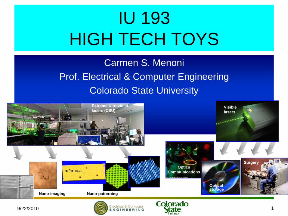
IU 193
HIGH TECH TOYS
Carmen S. Menoni
Prof. Electrical & Computer Engineering
Colorado State University
Optics
Communications
Optical storage
Surgery
Visible
lasers
Extreme Ultraviolet
lasers (CSU)
Nano-imaging
82nm82nm
Nano-patterning

9/22/2010 2
Syllabus
• Course description:
Students are introduced to the major scientific breakthroughs that have
made impact in many areas of science and technology. Emphasis will be
given to technologies that made possible the engineering of communication
networks like the internet. Key concepts of waves, light generation and
detection, optical and wireless communication will be covered. Other
technologies that have revolutionized mankind will also be explored.
• Course credits: 1
• Prerequisites: None
• Course Goals: i) To make students appreciate technology and the science
that makes this technology possible in a way that is simple and intuitive; ii)
to instill curiosity; iii) to develop communication skills through written and
oral presentations; iv) to learn the use of the library and specialized search
engines.
•

9/22/2010 3
• Course Outline:
1. Waves: what are they, how are they generated?
2. Different types of waves: radio, microwave, light signals.
3. Lasers- 50th anniversary
4. Lasers in communication, medicine and industry
5. Silicon technology and its impact.
6. Students turn in their final report and hold their oral presentation
Syllabus

9/22/2010 4
• Homework: Homework will be assigned each week. It will consist of short research papers
related to the class topics. Every Tuesday the New York Times publishes the ‘Science” section.
Students will be required to pick an article of their choice related to advances in science and
technology and write a short review ( 300 words). No late homework will be accepted.
• Research Paper: Students will form teams of up to three and research on a High Tech Toy of
their interest. They will write an essay ( 1000 words) and compose a power-point presentation
that will be presented in class the last week of classes.
• In-class participation: Students will be expected to pro-actively contribute to discussions at the
small group and whole class levels; to keep a notebook with up-to-date class notes; to be
prepared for class with assignments and required class material. Short quizzes will be given.
• Additional Elective Activities: The instructor of this class has a strong appreciation for the arts
and will share these interests with the students by inviting them to concerts organized by the
Music Department, Art exhibitions by the Art Department, and movies that are part of CSU ASAP
Cinema series.
• Grading: 60 % Homework
• 15 % In-class participation – includes quiz grade
• 25 % Research Paper – written and oral presentation
•
Syllabus
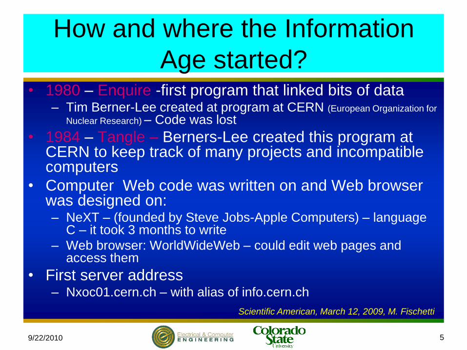
9/22/2010 5
How and where the Information
Age started? • 1980 – Enquire -first program that linked bits of data
– Tim Berner-Lee created at program at CERN (European Organization for
Nuclear Research) – Code was lost
• 1984 – Tangle – Berners-Lee created this program at CERN to keep track of many projects and incompatible computers
• Computer Web code was written on and Web browser was designed on: – NeXT – (founded by Steve Jobs-Apple Computers) – language
C – it took 3 months to write
– Web browser: WorldWideWeb – could edit web pages and access them
• First server address – Nxoc01.cern.ch – with alias of info.cern.ch
Scientific American, March 12, 2009, M. Fischetti

9/22/2010 6
How and where the Information
Age started?
• First full demonstration
– Christmas Day 1990, operating from Berners-Lee
NeXT machine to the NeXT computer of his partner
and now Web-developer Robert Cailliau
• Content of first Web page:
– The CERN phone directory
• Hits on the pages – August 1991: 100 a day- August 1993 –
10,000 a day
• First U.S. Web server
– April 1991, Stanford University Linear Accelerator Lab
Scientific American, March 12, 2009, M. Fischetti

9/22/2010 7
How and where the Information
Age started?
• First Web browsers
– WorldWideWeb – Dec. 1990 – NeXT platform - Berners-Lee –
– Erwise – April 1992 – UNIX platform – students at Helsinki University
– Viola, May 1992 – student Pei Wei, UC Berkeley
– Samba, Summer 1992 – Macintosh by Robert Caillau, CERN
– Netscape, Yahoo, Google and ……… Scientific American, March 12, 2009, M. Fischetti

9/22/2010 8
What are the technologies that make
possible the World Wide Web?
• In class exercise: Students’ input
Satellites Fiber optics and lasers
Cables
Computers
Computer programs
Programming languages and codes
Electrical power

9/22/2010 9
Mapping the internet
Nodes worldwide
• http://www.technologyreview.com/Infotech/
18944/?a=f The shape of the online universe.
This image shows the hierarchical
structure of the Internet, based on the
connections between individual nodes
(such as service providers). Three
distinct regions are apparent: an inner
core of highly connected nodes, an
outer periphery of isolated networks,
and a mantle-like mass of peer-
connected nodes. The bigger the node,
the more connections it has. Those
nodes that are closest to the center are
connected to more well-connected
nodes than are those on the periphery.
Lanet-vi program of I. Alvarez-Hamelin et al.

9/22/2010 10
The core: At the center of the
Internet are about 80 core nodes
through which most traffic flows.
Remove the core, and 70 percent
of the other nodes are still able to
function through peer-to-peer
connections.
Mapping the internet
Nodes worldwide

9/22/2010 11
The periphery: At the very
edge of the Internet are 5,000
or so isolated nodes that are
the most dependent upon the
core and become cut off if the
core is removed or shut
down. Yet those nodes within
this periphery are able to stay
connected because of their
peer-to-peer connections.
Mapping the internet
Nodes worldwide

9/22/2010 12
Providers red
• USA web
http://advice.cio.com/theme
s/CIO.com/cache/Internet_
map_labels_0.pdf

Global internet maps http://www.google.com/imgres?imgurl=http://api.ning.com/files/tkxN4I-yyJH5HfiQkY40TPi9M7UNQSNpyDdqEsAbIJrQK-
nMqXH7Le607NBRdtE0Lt7gqaOrvfG89mj-
Vt8QH48hoPqF7aVJ/globalinternetmaptelegeog.gif&imgrefurl=http://visualthinkmap.ning.com/photo/global-internet-
map&usg=__DR4kglL1Fpopgi1TgwjZmcxxuoo=&h=855&w=1200&sz=172&hl=en&start=0&zoom=1&tbnid=r4O51fwvMo_Z9M:&tb
nh=155&tbnw=218&prev=/images%3Fq%3Dglobal%2Binternet%2Bmap%26um%3D1%26hl%3Den%26client%3Dfirefox-
a%26sa%3DX%26rls%3Dorg.mozilla:en-
US:official%26biw%3D1400%26bih%3D837%26tbs%3Disch:1&um=1&itbs=1&iact=rc&dur=468&ei=gJmHTPrTE4SksQO8j6SMC
g&oei=gJmHTPrTE4SksQO8j6SMCg&esq=1&page=1&ndsp=23&ved=1t:429,r:0,s:0&tx=119&ty=93
9/22/2010 13

9/22/2010 14
Week 2
• Signals – how do one can transmit
information?
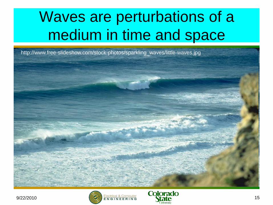
9/22/2010 15
Waves are perturbations of a
medium in time and space http://www.free-slideshow.com/stock-photos/sparkling_waves/little-waves.jpg
9/22/2010 16
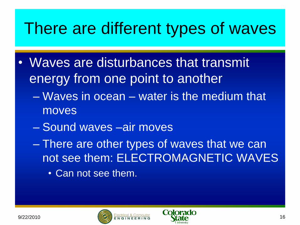
There are different types of waves
• Waves are disturbances that transmit
energy from one point to another
– Waves in ocean – water is the medium that
moves
– Sound waves –air moves
– There are other types of waves that we can
not see them: ELECTROMAGNETIC WAVES
• Can not see them.

9/22/2010 17
Electromagnetic Waves (the
electromagnetic spectrum)
• These waves originate from moving electrons
• They have been exploited in many applications
Radar
Fiber optics
Welding
Data
storage
X-rays
imaging
CAT scan
imaging Nano-imaging and
patterning (CSU)
Light
9/22/2010 18
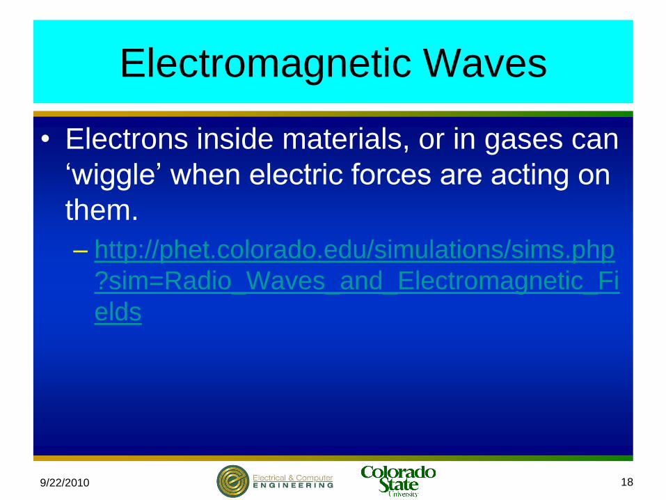
Electromagnetic Waves
• Electrons inside materials, or in gases can
‘wiggle’ when electric forces are acting on
them.
– http://phet.colorado.edu/simulations/sims.php
?sim=Radio_Waves_and_Electromagnetic_Fi
elds
9/22/2010 19
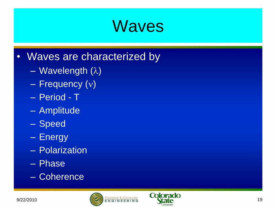
Waves
• Waves are characterized by
– Wavelength ( )
– Frequency ( )
– Period - T
– Amplitude
– Speed
– Energy
– Polarization
– Phase
– Coherence
9/22/2010 20
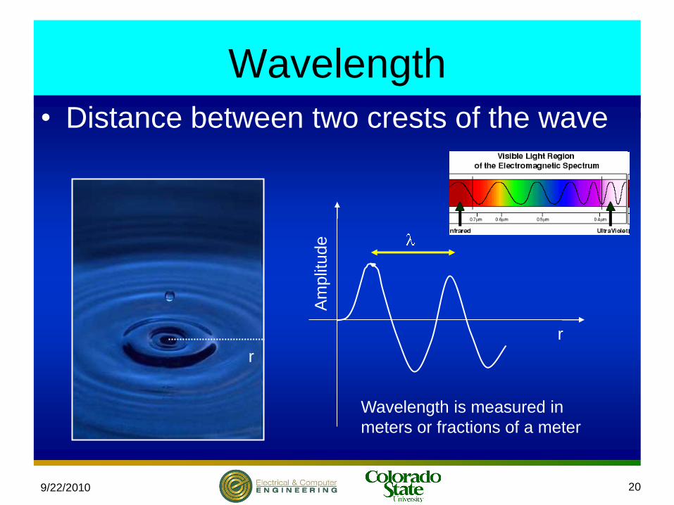
Wavelength
• Distance between two crests of the wave
r
r
Am
plit
ude
Wavelength is measured in
meters or fractions of a meter

9/22/2010 21
Waves can be periodic or aperiodic
Periodic
wave
Aperiodic wave
Periodic wave
space

9/22/2010 22
Period and Frequency
• For periodic waves, we can identify a period, T, by measuring the time taken for a wavelength to pass a given point
• The frequency, , is the inverse of the period i.e.
= 1/T
• and is the number of times per second that an oscillation occurs at any fixed point in space
Am
plit
ude
time
Period is measured in seconds
or fractions of a second
Frequency is inverse of time is
measured in Hertz.
T

9/22/2010 23
Prefixes used in units of
wavelength, Time and Frequency
Prefix Symbol Value Wavelength
(m)
Time (sec) Frequency
(Hz)
Tera T 1012 THz
Giga G 109 GHz
Mega M 106 MHz
kilo k 103 kHz
milli m 10-3 mm ms
micro 10-6 m s
nano n 10-9 nm ns
pico p 10-12 pm ps
femto f 10-15 fs

9/22/2010 24
Comparison of wavelengths across the
electromagnetic spectrum to other objects
http://mc2.gulf-pixels.com/wp-content/uploads/2009/07/Electromagnetic-Spectrum2.jpg

9/22/2010 25
Speed
• The speed of a wave is calculated from
the distance it travels in one period ( )
divided by the period
Am
plit
ude
distance
on off c: speed of
electromagnetic signals in
vacuum is 3x10⁸ m/s
http://phet.colorado.edu/simulations
/sims.php?sim=Wave_Interference

9/22/2010 26
Energy
• Waves carry energy –
– Fluence in Joules per square cm is used to
measure energy density
– Intensity in Watts per square cm is used to
measure power density

9/22/2010 27
Polarization
• In electromagnetic signals the electric field
oscillates in specific directions. This is
called polarization. We exploit this to filter
light for example with sunglasses.
http://www.colorado.edu/physics/2000
/applets/polarized.html

9/22/2010 28
Phase and coherence
ALL SIGNALS REACH
MAXIMUM AT THE
SAME TIME AND
SAME LOCATION IN
SPACE – SIGNALS
HAVE SAME PHASE.
THESE SIGNALS ARE
COHERENT distance
These two signals are
not in phase –
They are INCOHERENT

9/22/2010 29
Light emitters for communication systems
LIGHT EMITTING DIODES AND LASERS
• SOURCES OF MONOCHROMATIC (ONE
COLOR) LIGHT
• POWERED BY ELECTRICITY OR
OTHER LIGHT SOURCES , THEY
GENERATE LIGHT
– LIGHT EMITTING DIODES: INCOHERENT
LIGHT
– LASERS –(Light Amplification by Stimulated
Emission of Radiation): COHERENT LIGHT

9/22/2010 30
LIGHT GENERATION How is light made?
atom
Add
energy
Add
energy
Material –
could be a
gas, solid or
liquid
Material –
could be a
gas, solid or
liquid
After some time
Light is emitted
Atom
electron
nucleus
1Atom
electron
nucleus
1
electron
nucleus
electron
nucleus
1 22
333

9/22/2010 31
LIGHT GENERATION VIA
ELECTRICAL DISCHARGE
http://phet.colorado.edu/simulations/sims.php?sim=Neon_Lights_
and_Other_Discharge_Lamps
Filament
atom electron
Gas
Light out
+ - battery

9/22/2010 32
LIGHT EMITTING DIODES
+ -
battery
Solid
material
current Light out
Solid State Materials:
semiconductors such as GaN, AlGaN

9/22/2010 33
Applications: solid state lightening
http://www.osram-os.com
Roadside illumination Landscape illumination
LEDs
consume
less
electricity
and last
much
longer than
light-bulbs

9/22/2010 34
Applications: solid state lightening
Car designer Fioravanti’s Yak concept
vehicle demonstrates the potential of LED-
style headlamps.
Electronic Design • May 13, 2002
Osram LEDs are prominent in this latest
Ford car.
http://optics.org

9/22/2010 35
LASER: Principle of operation
Energy
mirrors
With mirrors the light emitted is
highly directional and coherent
Light out
http://phet.colorado.edu/simulations/sims.php?sim=Lasers

9/22/2010 36
Laser diodes used for
communications
• They are small and efficient
• They operate in the infrared range (1.3-1.5
m for long haul communications)

9/22/2010 37
• The emission wavelength of the laser is
selected to minimize absorption and
dispersion in the fiber optics that carry the
signal generated by the laser
Laser diodes used for
communications
Attenuation: amplitude
of pulse decreases as it
travels through the fiber length
length
Dispersion: pulse
broadens in wavelengths
as it travels through the
fiber

Fiber optics are glass cables
capable to transmit light
9/22/2010 38
Light is transmitted by the
process of total internal
reflection. That is the light is
reflected from the inner walls
of the fiber.
http://communication.howstuffworks.com/fibe
r-optic-communications/fiber-optic.htm

Fiber optics communication
system
9/22/2010 39
Fiber spool Signal in
Signal out
Laser diode-
output
modulated Receiver
and
amplifier
station
(Er-doped
amplifiers)
Detector
Photodiode Band Description Wavelength Range
O band original 1260 to 1360 nm
E band extended 1360 to 1460 nm
S band short wavelengths 1460 to 1530 nm
C band conventional ("erbium window") 1530 to 1565 nm
L band long wavelengths 1565 to 1625 nm
U band ultralong wavelengths 1625 to 1675 nm

Advantages of fiber optics http://communication.howstuffworks.com/fiber-optic-communications/fiber-optic4.htm
• Less expensive - Several miles of optical cable can be made cheaper than
equivalent lengths of copper wire. This saves your provider (cable TV, Internet) and
you money.
• Thinner - Optical fibers can be drawn to smaller diameters than copper wire.
• Higher carrying capacity - Because optical fibers are thinner than copper wires,
more fibers can be bundled into a given-diameter cable than copper wires. This
allows more phone lines to go over the same cable or more channels to come
through the cable into your cable TV box.
• Less signal degradation - The loss of signal in optical fiber is less than in copper
wire.
• Light signals - Unlike electrical signals in copper wires, light signals from one fiber
do not interfere with those of other fibers in the same cable. This means clearer
phone conversations or TV reception.
• Low power - Because signals in optical fibers degrade less, lower-power transmitters
can be used instead of the high-voltage electrical transmitters needed for copper
wires. Again, this saves your provider and you money.
• Digital signals - Optical fibers are ideally suited for carrying digital information, which
is especially useful in computer networks.
• Non-flammable - Because no electricity is passed through optical fibers, there is no
fire hazard.
• Lightweight - An optical cable weighs less than a comparable copper wire cable.
Fiber-optic cables take up less space in the ground.
9/22/2010 40

Network of fiber optics communications
9/22/2010 41
http://www.eweek.com/c/a/IT-Infrastructure/Google-Helps-Finance-Latest-TransPacific-
Fiber-Optic-Cable-Project-307642/
http://www.eweek.com/c/a/IT-Infrastructure/Google-Helps-Finance-Latest-TransPacific-Fiber-Optic-
Cable-Project-307642/

Other applications of lasers http://www.laserfest.org/lasers/video-life.cfm
• Medicine
– Surgery, dermatology
• Biology
– Imaging/Microscopy
• Optics
– Interferometry, holography, microscopy, spectroscopy
• Atmospheric science
– Ranging and probing, LIDAR (light detection and ranging
• Materials science
– Cutting, welding, engraving, cleaning, lithography
9/22/2010 42
Movie from Laserfest

Lasers in medicine
• Optical Coherence Tomography – http://www.laserfest.org/lasers/innovations.cfm
– Optical Coherence Tomography is like ultrasound. The laser light penetrates below surface
of the human tissue and is reflected back. The laser reflection from the tissue is recorded
back. An image is constructed from the data. Multiple scans over a region yields a 3-D
image.
• Surgery
– Eye surgery – Excimer lasers (UV) sculpt the cornea (LASIK) –
Catarat removal
– Blood-less surgery (green laser cauterizes/ ligates vessels as it
cuts)
9/22/2010 43

Lasers used in material science
Ceramic Process Type of Laser Wavelength
Scribing, Drilling and
Profiling Fired Substrates
(Alumina, AlN, BeO)
CO2 10.9 m -10-100 W
Scribing, Drilling and
Profiling Green Substrates
CO2/UV-
DiodePumpedSolidSt
ate
10.9/0.2 m
Selective Material Removal YAG/Green/UV-DPSS
Marking/Serializing CO2 /YAG/Green/ UV-
DPSS
10.9/1.06/0.52/0.24
m
Lithography Excimer 0.197 m
9/22/2010 44

Lithography- How to make a Silicon
chip
• Photolithography is the technology used to print
semiconductor chips
9/22/2010 45
Samsung Flash Memory 30 Gb-
Prints 30 nm lines
System is like a microscope. It forms
a demagnified image of the mask

Lithography is an ultra-clean
process • In the US, Intel and GlobalFoundries
(previously AMD) fabricate chips
9/22/2010 46
http://wn.com/Silicon_Wafer_Processing_Animation
Cleanroom

What controls size of the small feature
that can be printed?
• UV lithography is reaching its limits
•
where k process dependent constant, NA is the
numerical aperture of the lens that focuses the light into
the wafer and creates the image of the mask
• NA of a lens can not be greater than 1. But it can be
increased using immersion. This is the way that current
chips with critical dimensions CD of 32 nm are preinted
using 196nm wavelength light from an excimer laser.
9/22/2010 47

Moore’s law The number of transistors that can be placed inexpensively on an
integrated circuit has doubled approximately every two years
9/22/2010 48

EUV Lithography will print 16nm features
and below – In production in 2014
• ASML making the printing tools with EUV
sources engineered by CYMER – Print
wavelength: 13.5 nm
9/22/2010 49

Elements of Printing process
• Wafer: Silicon ultrapolished and flat
• Mask: Glass with a pattern of Cr that is
fabricated with electron beam lithography
9/22/2010 50
Mask
Aligner

The lithographic process
• Process to transfer the mask pattern into the wafer
9/22/2010 51

Smallest periodic lines printed
on resist using EUV Lithography • Center of X-Ray Optics, Lawrence
Berkeley lab. - Sematech
9/22/2010 52
Nm period lines
on a mask are
needed to print
the gates of
transistors on a
chip

The transistor
In December 1947 three researchers demonstrated a device that
would change the way humankind works and plays
Scientific American: The Solid-State Century, 1997
9/22/2010 53
INVENTORS Shockley
(seated), Bardeen (left) and
Brattain (right) were the
first to demonstrate a solid-
state amplifier
1947
Late 50’s
Transistor is a device that can:
Control current –(switch)
Amplify current

What transistors have enabled
• Vacuum tube technology Transistor technology
9/22/2010 54
AM/FM readio from 50’s
AM/FM radio 2010

Transistors on a chip
• A transistor is used for switching, relaying, and amplifying electrical signals. In the
hydraulic world, this would be equivalent to a valve that can be opened and closed
with a separate pressure input, with a second one-way check valve on the output side
of the assembly. As more pressure is applied onto the control line, more fluid is
allowed to flow through the valves.
9/22/2010 55
METAL OXIDE FIELD EFFECT
TRANSISTOR
By applying a
voltage to the gate,
it is possible to
control the flow of
electrons from the
source to the drain
This is the
workhorse of data
processing

Microprocessors (CPU)
• A collection of transistors, and other elements, such as resistors,
capacitors diodes make up an electronic circuit or IC.
• A micro-processor is an IC that incorporatesfunctions. There is a
complex architecture design in the IC. The micro-processor or CPU
is the heart of a computer.
9/22/2010 56
IBM RS/6000
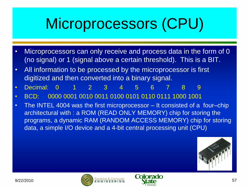
Microprocessors (CPU)
• Microprocessors can only receive and process data in the form of 0
(no signal) or 1 (signal above a certain threshold). This is a BIT.
• All information to be processed by the microprocessor is first
digitized and then converted into a binary signal.
• Decimal: 0 1 2 3 4 5 6 7 8 9
• BCD: 0000 0001 0010 0011 0100 0101 0110 0111 1000 1001
• The INTEL 4004 was the first microprocessor – It consisted of a four–chip
architectural with : a ROM (READ ONLY MEMORY) chip for storing the
programs, a dynamic RAM (RANDOM ACCESS MEMORY) chip for storing
data, a simple I/O device and a 4-bit central processing unit (CPU)
9/22/2010 57

Microprocessor evolution
Name Date Transistors
Microns (width
of transistor
gate)
Clock speed
(maximum rate
chip can be
clocked
Data width
(length of nibs)
MIPS (Millions of
Instructions per
second)
8080 1974 6,000 6 2 MHz 8 bits 0.64
8088 1979 29,000 3 5 MHz 16 bits
8-bit bus 0.33
80286 1982 134,000 1.5 6 MHz 16 bits 1
80386 1985 275,000 1.5 16 MHz 32 bits 5
80486 1989 1,200,000 1 25 MHz 32 bits 20
Pentium 1993 3,100,000 0.8 60 MHz 32 bits
64-bit bus 100
Pentium II 1997 7,500,000 0.35 233 MHz 32 bits
64-bit bus ~300
Pentium III 1999 9,500,000 0.25 450 MHz 32 bits
64-bit bus ~510
Pentium 4 2000 42,000,000 0.18 1.5 GHz 32 bits
64-bit bus ~1,700
Pentium 4
"Prescott" 2004 125,000,000 0.09 3.6 GHz
32 bits
64-bit bus ~7,000
9/22/2010 58
Present technology in
high volume
manufacturing
Gate width: 32 nm

Intel newest technology
9/22/2010 59
Processor Clock
Speed(s)
Intro
Date(s)
Mfg.
Process
Transistor
s
Addressab
le Memory
Cache Bus
Speed
Typical
Use
Intel®
Core™2
Extreme
Q9000
2 GHz Dec-08 45nm 410 million 64 GB 6 MB 1066 MHz Enthusiast
Notebook
Intel®
Core™2
Duo
processor
T9800
2.93 GHz Dec-08 45nm 410 million 64 GB 6 MB 1066 MHz Mobile PC