Embed Size (px)
Citation preview

Cavity Photons as a Probe for Charge Relaxation Resistance and Photon Emissionin a Quantum Dot Coupled to Normal and Superconducting Continua
L. E. Bruhat,1 J. J. Viennot,1,2 M. C. Dartiailh,1 M.M. Desjardins,1 T. Kontos,1 and A. Cottet1,*1Laboratoire Pierre Aigrain, Ecole Normale Supérieure-PSL Research University, CNRS,
Université Pierre et Marie Curie-Sorbonne Universités, Université Paris Diderot-Sorbonne Paris Cité,24 rue Lhomond, F-75231 Paris Cedex 05, France
2JILA and Department of Physics, University of Colorado, Boulder, Colorado 80309, USA(Received 11 November 2015; revised manuscript received 4 March 2016; published 9 May 2016)
Microwave cavities have been widely used to investigate the behavior of closed few-level systems. Here,we show that they also represent a powerful probe for the dynamics of charge transfer between a discreteelectronic level and fermionic continua. We have combined experiment and theory for a carbon nanotubequantum dot coupled to normal metal and superconducting contacts. In equilibrium conditions, where ourdevice behaves as an effective quantum dot-normal metal junction, we approach a universal photondissipation regime governed by a quantum charge relaxation effect. We observe how photon dissipation ismodified when the dot admittance turns from capacitive to inductive. When the fermionic reservoirs arevoltage biased, the dot can even cause photon emission due to inelastic tunneling to/from a Bardeen-Cooper-Schrieffer peak in the density of states of the superconducting contact. We can model thesenumerous effects quantitatively in terms of the charge susceptibility of the quantum dot circuit.This validates an approach that could be used to study a wide class of mesoscopic QED devices.
DOI: 10.1103/PhysRevX.6.021014 Subject Areas: Optics, Quantum Physics,Semiconductor Physics
I. INTRODUCTION
Circuit QED techniques [1] have recently been putforward to investigate the electronic dynamics in quantumdot circuits [2–4] or, more generally, mesoscopic circuits[5]. So far, the interaction between cavity photons andcharges [6–16] or spins [17] confined in quantum dots hasreceived the most experimental attention. This atomiclikelimit is a priori very appealing for quantum informationapplications since it goes, in principle, with long coherencetimes. Nevertheless, mesoscopic circuits are inseparablefrom the existence of electronic reservoirs with Fermi seas.These fermionic reservoirs are not necessarily a drawback.For instance, a strong coupling between a dot and a normalmetal enables one to revisit condensed matter problemssuch as the Kondo effect. Ferromagnetic contacts can beused to design spin quantum bits [17] or to study spin-dependent transport [18]. Superconducting contacts arecrucial for the study of Cooper pair splitting [19,20],Andreev bound states [21–23], and Majorana quasiparticles[24]. In principle, microwave cavities could represent apowerful tool to investigate these features [25–32].
In this context, it is crucial to understand how tunnelingprocesses between a discrete energy level and the con-tinuum of states of a reservoir can affect cavity photons.This situation is epitomized by a single quantum dot circuitcoupled to a cavity, a case that has been studied elusivelyso far [3,8,33]. A recent experiment has revealed that thequantum dot can add an effective capacitance or aninductance to the photon environment, depending on thetransparency of its contacts [8]. However, the cavitydissipation expected, together with this effect, has beenleft unexplored. On the theory side, most experimentscombining quantum dot circuits and microwave resonatorshave been interpreted by disregarding fermionic reservoirsor by using a Lindbladt equation suitable for dot-reservoirtunnel rates much smaller than the temperature of theexperiment. An alternative approach is highly desirable forinvestigating the open contacts limit. Descriptions in termsof the charge susceptibility of the quantum dot circuits haverecently been suggested [5,34–36].In this work, we study experimentally and theoretically
the behavior of a single quantum dot in a carbon nanotube,coupled to normal metal (N) and superconducting (S)reservoirs, and embedded in a high finesse microwavecavity. In a first step, we study a dot with a discrete levelcoupled only to the N reservoir. In this case, the currentresponse of the dot to a direct gate voltage excitation Vrfcan be developed as Irf ¼ iωrfCQð1 − iωrfRacCQÞVrf þoðω2
rfÞ, provided the frequency ωrf of the excitation issmaller than the tunnel rate ΓN of the N-dot junction.
*Corresponding [email protected]
Published by the American Physical Society under the terms ofthe Creative Commons Attribution 3.0 License. Further distri-bution of this work must maintain attribution to the author(s) andthe published article’s title, journal citation, and DOI.
PHYSICAL REVIEW X 6, 021014 (2016)
2160-3308=16=6(2)=021014(16) 021014-1 Published by the American Physical Society
This development maps onto that expected for a RC circuitwith capacitance CQ and resistance Rac. The capacitanceCQ characterizes the ability of the dot to host electrons at dcor low frequencies. The resistance Rac describes thedynamics of charge tunneling through the junction, whichleads to the relaxation of the charge imbalance caused byVrf . For an incoherent device, Rac depends on the detailedproperties of the dot circuit. However, in the coherentnoninteracting limit with ωrf ≪ ΓN , Büttiker and cowork-ers have predicted that Rac should take a universal value,independently of the dot parameters [37,38]. This effect,which reveals the wavy behavior of electrons inside the dot,is of fundamental as well as practical importance in thecontext of the miniaturization of electronic devices. Theonly observation of a universal Rac so far was performed byGabelli et al. with a strongly spin-polarized GaAs quantumdot, using ac conductance measurements [39]. Remarkably,this dot was in a noninteracting regime because of a topgate with an unusually large capacitance [40]. Noticeably,the independence of Rac from the dot orbital energy was nottested by Gabelli and coworkers. In our system, thisproperty appears as a scaling between the dissipationand dispersion induced by the dot on the cavity. We canexperimentally confirm this scaling behavior for intermedi-ate tunnel rates ΓN ∼ 2.5ωrf , where it is already approx-imately valid and well resolvable. Remarkably, this effectoccurs in spite of the presence of strong Coulomb blockadein our sample. The effect of interactions on quantum chargerelaxation has caused intense theoretical activity because,in practice, most quantum dots are subject to strongCoulomb interactions. In this limit, predictions for Racdisplay a rich phenomenology [41–47]. Nevertheless, itwas recently suggested that a universal charge relaxationresistance persists in the spin-degenerate interacting case[45,46]. Our results are consistent with this prediction.Finally, we observe how quantum charge relaxationdepends on the dot orbital energy for smaller tunnel rates,when the dot admittance turns from capacitive to inductive.In a second step, we study the finite bias voltage regime
where the dot level is also coupled to the S reservoir.Contextually, the implementation of mesoscopic QEDexperiments with superconducting hybrid circuits is veryrecent. Atomic contacts between superconductors havebeen used to form a new type of quantum bit based onAndreev bound states [23]. Semiconducting nanowireshave been used for realizing Josephson junctions in super-conducting circuits [48,49]. However, quantum dot circuitswith superconducting reservoirs have been coupled neitherto microwave cavities nor to a direct ac excitation, so far.Despite this lack of experiments, photon-assisted tunnelingbetween a dot and a superconductor has created theoreticalinterest for more than 15 years [50–59]. The couplingbetween superconductor-quantum dot hybrid circuits andmicrowave cavities has also been studied in recent theo-retical works [25–27]. Here, we show experimentally that a
microwave cavity is able to reveal photon-assisted tunnelevents between a dot and the Bardeen-Cooper-Schrieffer(BCS) peaks of a superconductor, not visible in the dotcurrent. In particular, we observe negative photon damping,which reveals photon emission. This result illustrates thatquasiparticle tunneling to a fermionic reservoir does notalways induce photonic dissipation.In order to understand our measurements, we use a
Keldysh Green’s function approach. We can simultane-ously reproduce the quantum dot conductance and themicrowave response of the cavity, versus the dot gate andbias voltages, with an unprecedented accuracy for this typeof hybrid system. We thereby validate the description ofmesoscopic QED experiments in terms of an electroniccharge susceptibility. To illustrate the broad scope of thisapproach, we present its multidot generalization, which canbe used for many different geometries, for instance, Cooperpair splitters and topological hybrid nanocircuits. Our workalso gives wide experimental perspectives since microwavecavities appear as a powerful probe for quantum chargerelaxation, photon-assisted tunneling, and all other effectsinvolving tunneling between a discrete level and fermionicreservoirs.This article is organized as follows. Section II presents
our experimental setup. Sections III and IV analyze ourexperimental data, for the N-dot and N-dot-S limits,respectively. Section V summarizes our results, presentsthe multidot generalization of our approach, and givesvarious perspectives. Appendix A shows experimentaldetails and supplementary data. Appendix B discussesour theoretical approach.
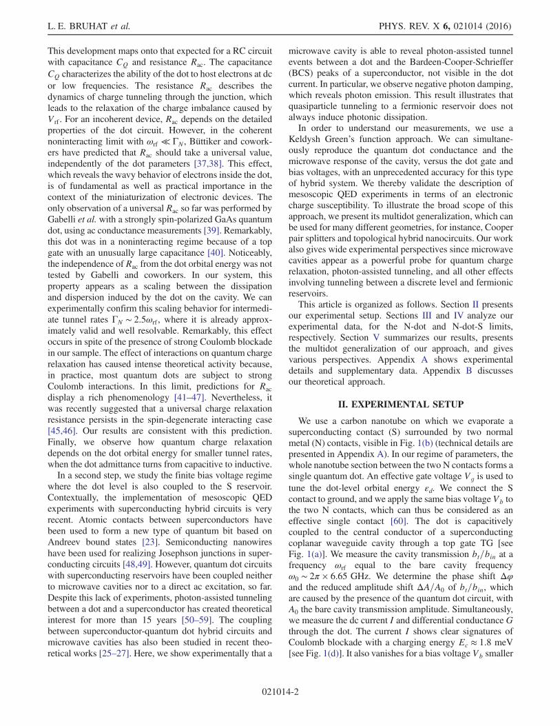
II. EXPERIMENTAL SETUP
We use a carbon nanotube on which we evaporate asuperconducting contact (S) surrounded by two normalmetal (N) contacts, visible in Fig. 1(b) (technical details arepresented in Appendix A). In our regime of parameters, thewhole nanotube section between the two N contacts forms asingle quantum dot. An effective gate voltage Vg is used totune the dot-level orbital energy εd. We connect the Scontact to ground, and we apply the same bias voltage Vb tothe two N contacts, which can thus be considered as aneffective single contact [60]. The dot is capacitivelycoupled to the central conductor of a superconductingcoplanar waveguide cavity through a top gate TG [seeFig. 1(a)]. We measure the cavity transmission bt=bin at afrequency ωrf equal to the bare cavity frequencyω0 ∼ 2π × 6.65 GHz. We determine the phase shift Δφand the reduced amplitude shift ΔA=A0 of bt=bin, whichare caused by the presence of the quantum dot circuit, withA0 the bare cavity transmission amplitude. Simultaneously,we measure the dc current I and differential conductance Gthrough the dot. The current I shows clear signatures ofCoulomb blockade with a charging energy Ec ≈ 1.8 meV[see Fig. 1(d)]. It also vanishes for a bias voltage Vb smaller
L. E. BRUHAT et al. PHYS. REV. X 6, 021014 (2016)
021014-2

than the gap Δ≃ 0.17 meV of the S contact. Therefore, forVb ¼ 0, the effect of the S contact can be disregarded, andthe quantum dot circuit corresponds to an effective N-dotjunction, studied in Sec. III. For ejVbj > Δ, our deviceenables the study of quasiparticle transport in a N-dot-Sbijunction, presented in Sec. IV.
III. PHOTON DISSIPATION IN AN EFFECTIVEN-DOT JUNCTION
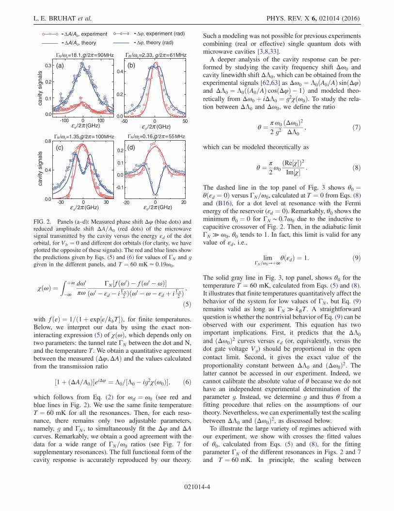
A single dot level coupled to a N reservoir is the mostbasic configuration for studying the light matter interactionin a mesoscopic circuit. Our device realizes such a situationfor Vb ¼ 0 due to the absence of subgap Andreev reflec-tions. Figure 2 shows the cavity signals Δφ (blue dots) andΔA=A0 (red dots) versus the energy εd of the dot orbital, forVb ¼ 0, and decreasing tunnel rates ΓN from left to rightand top to bottom panels. The correspondence between εdand the gate voltage Vg is given in Appendix A for each dotlevel. We observe resonances, although I ¼ 0. This meansthat the cavity is able to reveal quasiparticle tunnelingbetween the dot and the N contact even if it does not lead toa dc current. The phase signal Δφ (blue dots) can bepositive as well as negative, as already observed in Ref. [8],depending on the value of ΓN . This is because, forω0 ≪ ΓN , the quantum dot circuit behaves as an effectivecapacitance. Electrons can very rapidly follow the varia-tions of the dot potential to go in and out of the dot,proportionally to the dot density of states. However, forω0 ≫ ΓN , the charge current lags behind the dot potential,so the dot behavior becomes inductive [37,61]. In contrast,
the signal ΔA (red dots) always remains negative, up toexperimental uncertainty. One could naively expect thatΔA, which reveals photon dissipation, will scale with ΓN ,which is the main dissipation parameter in our problem.However, this intuition is wrong since ΔA becomes smallwhen ΓN tends to large values [see Fig. 2(a)].To understand the behavior of our device, we use the
Hamiltonian
Htot ¼ Hd þ ω0a†aþ gðaþ a†ÞXσ
d†σdσ
þXp
ωpb†pbp þ
Xp
ðτpb†paþ τ�pa†bpÞ; ð1Þ
where Hd describes the quantum dot circuit (seeAppendix B for details), d†σ adds an electron with spin σin the dot level, a† adds a photon in the cavity, and b†pdescribes a bosonic bath that accounts for the cavityintrinsic linewidth Λ0. We assume that cavity photonsmodulate the chemical potential of the quantum dot witha coupling constant g ¼ eϰVrms, with Vrms the cavityroot-mean-square voltage and e the electron charge. Thedimensionless coupling constant ϰ depends on the overlapbetween the electron wave function associated with thedot level and the photonic pseudopotential, which isspatially nonuniform [5]. Therefore, the value of g gen-erally depends on the dot level considered, as we will see inthe experimental data. Using Eq. (1), a semiclassical linearresponse approach leads to the cavity transmission (seeAppendix B):
btbin
¼ t0ωrf − ω0 − iΛ0 − g2χðω0Þ
: ð2Þ
The quantum dot charge susceptibility χðωÞ can be calcu-lated within the Keldysh formalism as
χ�ðωÞ ¼ −iZ
dω2π
Tr½SðωÞGrðωÞΣ<ðωÞGaðωÞ�; ð3Þ
with
SðωÞ ¼ τ½Grðωþ ω0Þ þ Gaðω − ω0Þ�τ: ð4Þ
The retarded and advanced Green’s functions Gr=a of thequantum dot and the lesser self-energy Σ<ðωÞ are definedin Appendix B. The matrix τ ¼ diagð1;−1Þ describes thestructure of the photon-particle coupling in the Nambu(electron-hole) space. Note that this degree of freedom isnot necessary for describing the N-dot junction, but weintroduce it for later use in Sec. IV. In the present section,we disregard the S reservoir and use Ec ¼ 0 so that thesusceptibility χðωÞ can be simplified as Eq. (B16) ofAppendix B at zero temperature and
TG
10 μm
ground
reso
nat
or
IVR
g VbV L
gVb
nanotube
1 μm
TG
tt
Ndot
bin
br
bt
(c)(a)
(b)
Vg (V)
Ec e
V b(m
V)
2Δe
I (nA)
2
-1
0
1
-2 -1
-0.2
0
(d)
S
0.2
0.4
0.6
0.8
FIG. 1. Panels (a) and (b): Scanning electron micrograph of themicrowave resonator and the quantum dot circuit. Panel (c):Principle of our setup. The dot level is tunnel coupled to the Nand S reservoirs and modulated by the cavity electric field. Panel(d): Current through the S contact versus the effective gatevoltage Vg and the bias voltage Vb.
CAVITY PHOTONS AS A PROBE FOR CHARGE … PHYS. REV. X 6, 021014 (2016)
021014-3
χðωÞ ¼Z þ∞
−∞dω0
πω
ΓN ½fðω0Þ − fðω0 − ωÞ�ðω0 − εd − i ΓN
2Þðω0 − ω − εd þ i ΓN
2Þ ;
ð5Þ
with fðεÞ ¼ 1=ð1þ exp½ε=kbT�Þ, for finite temperatures.Below, we interpret our data by using the exact non-interacting expression (5) of χðωÞ, which depends only ontwo parameters: the tunnel rate ΓN between the dot and N,and the temperature T. We obtain a quantitative agreementbetween the measured ðΔφ;ΔAÞ and the values calculatedfrom the transmission ratio
½1þ ðΔA=A0Þ�eiΔφ ¼ Λ0=½Λ0 − ig2χðω0Þ�; ð6Þ
which follows from Eq. (2) for ωrf ¼ ω0 (see red andblue lines in Fig. 2). We use the same finite temperatureT ¼ 60 mK for all the resonances. Then, for each reso-nance, there remains only two adjustable parameters,namely, g and ΓN , to simultaneously fit the Δφ and ΔAcurves. Remarkably, we obtain a good agreement with thedata for a wide range of ΓN=ω0 ratios (see Fig. 7 forsupplementary resonances). The full functional form of thecavity response is accurately reproduced by our theory.
Such a modeling was not possible for previous experimentscombining (real or effective) single quantum dots withmicrowave cavities [3,8,33].A deeper analysis of the cavity response can be per-
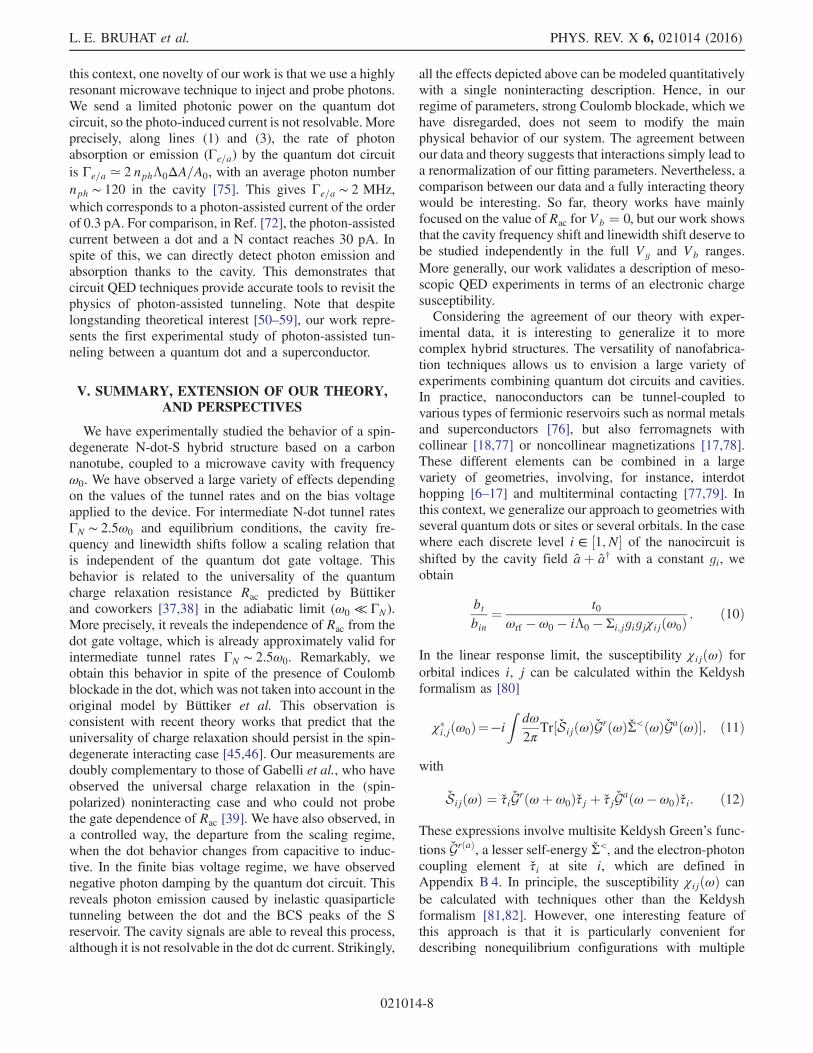
formed by studying the cavity frequency shift Δω0 andcavity linewidth shift ΔΛ0, which can be obtained from theexperimental signals [62,63] as Δω0 ¼ Λ0ðA0=AÞ sinðΔφÞand ΔΛ0 ¼ Λ0ððA0=AÞ cosðΔφÞ − 1Þ and modeled theo-retically from Δω0 þ iΔΛ0 ¼ g2χðω0Þ. To study the rela-tion between ΔΛ0 and Δω0, we define the ratio
θ ¼ π
2
ω0
g2ðΔω0Þ2ΔΛ0
; ð7Þ
which can be modeled theoretically as
θ ¼ π
2ω0
ðRe½χ�Þ2Im½χ� : ð8Þ
The dashed line in the top panel of Fig. 3 shows θ0 ¼θðεd ¼ 0Þ versus ΓN=ω0, calculated at T ¼ 0 from Eqs. (8)and (B16), for a dot level at resonance with the Fermienergy of the reservoir (εd ¼ 0). Remarkably, θ0 shows theminimum θ0 ¼ 0 for ΓN ∼ 0.7ω0 due to the inductive tocapacitive crossover of Fig. 2. Then, in the adiabatic limitΓN ≫ ω0, θ0 tends to 1. In fact, this limit is valid for anyvalue of εd, i.e.,
limΓN=ω0→þ∞
θðεdÞ ¼ 1: ð9Þ
The solid gray line in Fig. 3, top panel, shows θ0 for thetemperature T ¼ 60 mK, calculated from Eqs. (5) and (8).It illustrates that finite temperatures quantitatively affect thebehavior of the system for low values of ΓN , but Eq. (9)remains valid as long as ΓN ≫ kBT. A straightforwardquestion is whether the nontrivial behavior of Eq. (9) can beobserved with our experiment. This equation has twoimportant implications. First, it predicts that the ΔΛ0
and ðΔω0Þ2 curves versus εd (or, equivalently, versus thedot gate voltage Vg) should be proportional in the opencontact limit. Second, it gives the exact value of theproportionality constant between ΔΛ0 and ðΔω0Þ2. Thelatter cannot be accessed in our experiment. Indeed, wecannot calibrate the absolute value of θ because we do nothave an independent experimental determination of theparameter g. Instead, we determine g and thus θ from afitting procedure that relies on the assumptions of ourtheory. Nevertheless, we can experimentally test the scalingbetween ΔΛ0 and ðΔω0Þ2, as discussed below.To illustrate the large variety of regimes achieved with
our experiment, we show with crosses the fitted valuesof θ0, calculated from Eqs. (5) and (8), for the fittingparameter ΓN of the different resonances in Figs. 2 and 7and T ¼ 60 mK. In principle, the scaling between
-50 0 500.0
0.2
0.4
ΓN /ω0=2.33, g /2π=61MHz
εd /2π (GHz)
- ΔA/A0, theory
- Δϕ, experiment (rad)- ΔA/A0, experiment
- Δϕ, theory (rad)
-20 0 20
-0.1
0.0
0.1
0.2
ΓN /ω0=0.16, g /2π=55MHz
εd /2π (GHz)-30 0 30
0.0
0.4
0.8
εd /2π (GHz)
ΓN /ω0=1.35, g /2π=100MHz
-100 0 1000.0
0.1
0.2
0.3
εd /2π (GHz)
ΓN /ω0=18.1, g /2π=90MHz
cavi
ty s
igna
lsca
vity
sig
nals
(a) (b)
(c) (d)
FIG. 2. Panels (a–d): Measured phase shift Δφ (blue dots) andreduced amplitude shift ΔA=A0 (red dots) of the microwavesignal transmitted by the cavity versus the energy εd of the dotorbital, for Vb ¼ 0 and different dot orbitals (for clarity, we haveplotted the opposite of these signals). The red and blue lines showthe predictions given by Eqs. (5) and (6) for values of ΓN and ggiven in the different panels, and T ¼ 60 mK≃ 0.19ω0.
L. E. BRUHAT et al. PHYS. REV. X 6, 021014 (2016)
021014-4

ΔΛ0 and ðΔω0Þ2 should be closely satisfied in the gray areawhere θ0 ≃ 1. However, for the two resonances we havefound in this area (ΓN ¼ 18.1ω0 and ΓN ¼ 14.3ω0), wecannot reliably determine ΔΛ0 from ΔA and Δφ becauseΔA is small and thus affected too much by backgroundvariations. This difficulty arises because in the adiabaticlimit, the dot charge is in phase with the dot gateexcitation, i.e., χðω0 ≪ ΓNÞ ¼ ℏ∂hni=∂εd ∈ R, with hnithe static charge occupation of the dot. This is why,for ΓN ≫ ω0, we find that ΔΛ0 ¼ g2Im½χðω0Þ� ∼8g2ðω0=ΓNÞ2=πω0 vanishes like ðω0=ΓNÞ2. FromRef. [63], ΔA is itself small in this case. Nevertheless,we can interpret the raw cavity signals Δφ and ΔA with thesame theory as our other data, which shows that they areconsistent with the universality of charge relaxation [see
Figs. 2(a) and 7]. To resolve the scaling behavior of thecavity response, we now consider the resonances at ΓN ¼2.40ω0 and ΓN ¼ 2.86ω0. These points belong to the pinkarea 2 ≤ ΓN ≲ 10 of Fig. 3, where, from our theory, thescaling behavior should still hold approximately, althoughθ0 < 1. As visible in Figs. 3(c) and 3(d), we indeed findthat the proportionality between the experimental ΔΛ0 andðΔω0Þ2 is satisfied to a good accuracy, with a scaling factorα ¼ πω0=2θ0g2. Small discrepancies between ΔΛ0 andαðΔω0Þ2 are visible in the theoretical curves (see red andblue lines) but not resolvable experimentally. Such ascaling behavior is observed here for the first time.Finally, we can observe how the scaling behavior breaksdown for smaller tunnel rates. When ΓN decreases, theðΔω0Þ2 peak versus εd first becomes wider than the ΔΛ0
peak (not shown) before becoming strongly nonmonotonic[see Figs. 3(a) and 3(b)].The remarkable scaling between ΔΛ0 and ðΔω0Þ2 is
directly related to the universality of the ac resistance of aquantum dot circuit, which was predicted by M. Büttikeret al. two decades ago [37,38] and recently revisited as aKorringa Shiba relation [43,45,64]. More precisely, for anoninteracting N-dot junction (Ec ¼ 0) excited at a fre-quency ωrf such that ΓN ≫ ωrf , kBT, the ac resistance is setby θðεdÞ, i.e., Rac ¼ h=4e2θðεdÞ, which gives Rac ¼ h=4e2
for our spin-degenerate case, for any gate voltage. Thiseffect can be understood as a quantum charge relaxationeffect, which involves the internal coherent dynamics of thequantum dot. So far, the universality of the quantum chargerelaxation has been observed only with a strongly spin-polarized GaAs two-dimensional electron gas device [39].Here, we present the second example of system, i.e., a spin-degenerate carbon nanotube device, whose behavior isconsistent with this phenomenon. Indeed, the scalingbehavior between ΔΛ0 and ðΔω0Þ2 reveals the independ-ence of Rac from the dot gate voltage Vg (or, equivalently,from the dot orbital energy εd), a property that could not beprobed in Ref. [39] and that is already valid for intermediatetunnel rates.The fact that we model the charge susceptibility of the
quantum dot circuit with a noninteracting model in spite ofCoulomb blockade is nontrivial. This approach is useful tounderstand our data because we are in a deep Coulombblockade regime (ΓN ≪ Ec), where correlation effectsinduced by interactions (e.g., the Kondo effect)are weak. In this limit, one can expect G and χ to showvariations similar to those of the noninteracting case, withonly quantitative modifications. In particular, a reduction ofthe amplitude of the signals is expected because of thereduction of the dot occupation by Coulomb blockade [65].Our results suggest that in our regime of parameters,interactions simply lead to a renormalization of our fittingparameters. In principle, it is possible to generalize ourmodel to the interacting case to quantitatively study theeffects of a finiteEc [65,66]. This is beyond the scope of the
0
θ0= 0.53
20
(c)
10
0.10
0.05
0.15
030
(b)
θ0= 0.140.6
0
0.3
εd /2π (GHz)
θ0= 0.130.04
0.08(a)
0
εd /2π (GHz)
(d)
ΓN /ω0
(b)
(d)
(a)
0.1 1 10
0.0
0.5
1.0
θ0
ΔΛ0
/2π,
α(Δ
ω0)
/2π
(MH
z)2
Uni
vers
al d
issi
patio
n
App
roxi
mat
e sc
alin
g
T = 0
T = 60 mK
fitted values for Figs. 2 & 6
(c)
θ0= 0.640.10
0.05
0.15
00 2010 30
0 10 0 2010
FIG. 3. Top panel: Ratio θ0 ¼ θðεd ¼ 0Þ versus the tunnel rateΓN , calculated from Eqs. (5), (8), and (B16) for T ¼ 0 (blackdashed line) and T ¼ 60 mK (gray solid line). The crossescorrespond to fitted values of θ0, calculated from Eqs. (5) and(8) for the different resonances in Figs. 2 and 7. Bottom panels:Comparison between the experimental ΔΛ0 and ðΔω0Þ2, usingthe scaling factor α ¼ πω0=2θ0g2, with θ0 indicated with arrowsin the top panel. We use ΓN=ω0 ¼ 0.16, 1.23, 2.33, and 2.86 fromleft to right and top to bottom panels. We also show, as blue andred solid lines, the calculated ΔΛ0 and ðΔω0Þ2.
CAVITY PHOTONS AS A PROBE FOR CHARGE … PHYS. REV. X 6, 021014 (2016)
021014-5
present article. Our observation of the scaling betweenΔΛ0
and ðΔω0Þ2 is independent of any theoretical assumptionon the dot interaction regime since the calculation of thesequantities from the raw data only relies on Eq. (2). The factthat we observe the scaling behavior between ΔΛ0 andðΔω0Þ2 in spite of a strong Coulomb blockade is remark-able. This is in agreement with recent theory works thatsuggest that the universality of the charge relaxationresistance Rac persists in the spin-degenerate interactingcase [45,46].
IV. NEGATIVE PHOTON DAMPINGBY A N-DOT-S BIJUNCTION
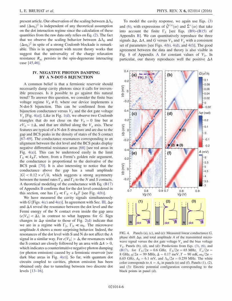
A common belief is that a fermionic reservoir shouldnecessarily damp cavity photons since it calls for irrevers-ible processes. Is it possible to go against this naturaltrend? To answer this question, we consider the finite biasvoltage regime Vb ≠ 0, where our device implements aN-dot-S bijunction. This can be confirmed from thebijunction conductance versus Vb and the dot gate voltageVg [Fig. 4(a)]. Like in Fig. 1(d), we observe two Coulombtriangles that do not close on the Vb ¼ 0 line but ateVb ∼�Δ, and that are shifted along the Vg axis. Thesefeatures are typical of a N-dot-S structure and are due to thegap and BCS peaks in the density of states of the S contact[67–69]. The conductance resonances corresponding to analignment between the dot level and the BCS peaks displaynegative differential resistance areas [68] [see red areas inFig. 4(a)]. This can be understood easily in the limitΓS ≪ kBT, where, from a Fermi’s golden rule argument,the conductance is proportional to the derivative of theBCS peak [70]. It is also interesting to notice that theconductance above the gap has a small amplitudejGj < 0.12 × e2=h, which suggests a strong asymmetrybetween the tunnel rates ΓN and ΓS to the N and S contacts.A theoretical modeling of the conductance with Eq. (B17)of Appendix B confirms that for the dot level considered inthis section, one has ΓS ≪ ΓN < kBT [see Fig. 4(b)].We have measured the cavity signals simultaneously
with G [Figs. 4(c) and 4(e)]. In agreement with Sec. III, Δφand ΔA reveal the resonance between the dot level and theFermi energy of the N contact even inside the gap area(ejVbj < Δ), in contrast to what happens for G. Signchanges in Δφ similar to those of Fig. 2(d) indicate thatwe are in a regime with ΓS, ΓN ≪ ω0. The microwaveamplitude A shows a more surprising behavior. Indeed, theresonances of the dot level with S and N do not affect the Asignal in a similar way. For ejVbj > Δ, the resonances withthe S contact are closely followed by an area with ΔA > 0,which indicates a counterintuitive negative photon damping(or photon emission) caused by a fermionic reservoir [seedark blue areas in Fig. 4(e)]. So far, with quantum dotcircuits coupled to cavities, photon emission has beenobtained only due to tunneling between two discrete dotlevels [13–16].
To model the cavity response, we again use Eqs. (3)and (6), with expressions of Gr=aðωÞ and Σ<ðωÞ that takeinto account the finite ΓS [see Eqs. (B9)–(B15) ofAppendix B]. We can quantitatively reproduce the threesignals Δφ, ΔA, and G versus Vb and Vg with a consistentset of parameters [see Figs. 4(b), 4(d), and 4(f)]. The goodagreement between the data and theory is also visible inFig. 8 of Appendix A for constant values of Vb. Inparticular, our theory reproduces well the positive ΔA
Vg (V)
-0.2
0
0.2
Vb
(mV
)
0.7
0.4(e)
Vg (V)0.7 0.90.9
6
5
4
4.5
3
5.5
3.5
(f)
-0.2
0
0.2V
b (m
V)
Δϕ (rad)0.4
(c)
0.2
0.1
0
-0.1
-0.2
-0.2
0
0.2
Vb
(mV
)
G (e / h)20.4
0
0.08
0.04
(1)
(3)(2)
(a) (b)
(d)
FIG. 5
A (mV)
dotdotNdotN
(1) (2) (3)
S
0.80.8
S SN
0.1
0.06
0.02
- 0.02
FIG. 4. Panels (a), (c), and (e): Measured linear conductance G,phase shift Δφ, and total amplitude A of the transmitted micro-wave signal versus the dot gate voltage Vg and the bias voltageVb. Panels (b), (d), and (d): Predictions from Eqs. (3), (6), and(B17), for ΓN=2π ¼ 0.6 GHz, ΓS=2π ¼ 65 MHz, Γn=2π ¼8 GHz, g=2π ¼ 99 MHz,Δ ¼ 0.17 meV, T ¼ 90 mK, ω0=2π ¼6.65 GHz, A0 ¼ 6.1 mV, and Λ0=2π ¼ 0.259 MHz. The whitecolor corresponds to A ¼ A0 in panels (e) and (f). Panels (1), (2),and (3): Electric potential configuration corresponding to theblack points in panel (d).
L. E. BRUHAT et al. PHYS. REV. X 6, 021014 (2016)
021014-6
areas. We take into account the lever arms determining theshift of the dot and reservoir energy levels with Vb and Vg.We also use the gap value Δ ¼ 0.17 meV given straight-forwardly by the GðVb; VgÞ map [69]. Then, only fiveadjustable parameters remain: ΓN , ΓS, g, T, and thebroadening parameter Γn for the BCS peaks.Simultaneously fitting three two-dimensional plots in theseconditions is nontrivial and possible only because of theadequacy of our model. The agreement with the data isoptimal for ΓN=2π ¼ 0.6 GHz, ΓS=2π ¼ 65 MHz,Γn=2π ¼ 8 GHz, g=2π ¼ 99 MHz, and T ¼ 90 mK.Equation (B17), used to model G, has been obtained inthe absence of the cavity (g ¼ 0). This approximation isrelevant because the cavity brings only small corrections tothis expression, not resolvable in our experiment. Incontrast, Δφ and A are calculated to second order in g.We have again used a noninteracting approach to model thedot behavior. This approximation is relevant to understandour data because we are in the deep Coulomb blockaderegime and because Andreev reflections (which are verysensitive to interactions) are negligible in the small ΓS limit.Therefore, interactions should only induce quantitativemodifications of the dot-lead resonances. Note that atemperature T ¼ 60 mK is optimal to interpret the lowbias voltage data of Sec. III, but we need a highertemperature T ¼ 90 mK to interpret the finite bias voltagedata of Sec. IV. This may be due to heating effects causedby Vb ≠ 0 or to interactions that can modify the dotoccupation and thus the amplitude of dot-lead resonancesin the out-of-equilibrium regime.Are the G < 0 and ΔA > 0 effects related? In order to
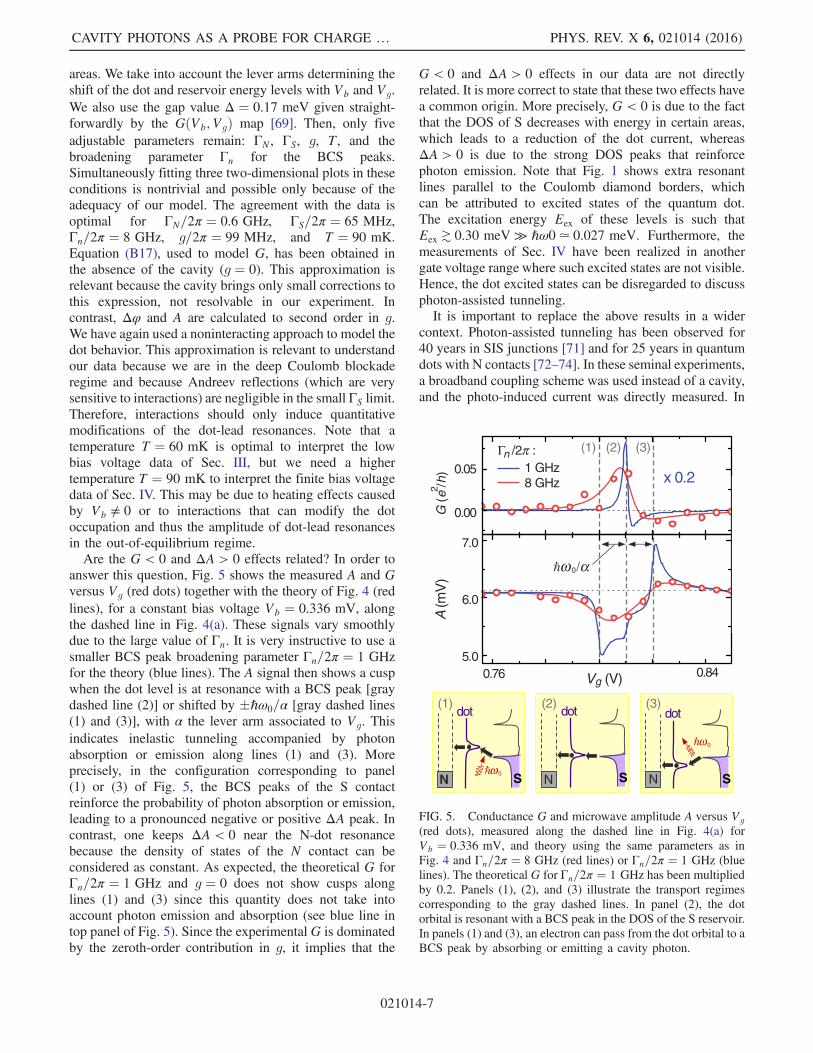
answer this question, Fig. 5 shows the measured A and Gversus Vg (red dots) together with the theory of Fig. 4 (redlines), for a constant bias voltage Vb ¼ 0.336 mV, alongthe dashed line in Fig. 4(a). These signals vary smoothlydue to the large value of Γn. It is very instructive to use asmaller BCS peak broadening parameter Γn=2π ¼ 1 GHzfor the theory (blue lines). The A signal then shows a cuspwhen the dot level is at resonance with a BCS peak [graydashed line (2)] or shifted by �ℏω0=α [gray dashed lines(1) and (3)], with α the lever arm associated to Vg. Thisindicates inelastic tunneling accompanied by photonabsorption or emission along lines (1) and (3). Moreprecisely, in the configuration corresponding to panel(1) or (3) of Fig. 5, the BCS peaks of the S contactreinforce the probability of photon absorption or emission,leading to a pronounced negative or positive ΔA peak. Incontrast, one keeps ΔA < 0 near the N-dot resonancebecause the density of states of the N contact can beconsidered as constant. As expected, the theoretical G forΓn=2π ¼ 1 GHz and g ¼ 0 does not show cusps alonglines (1) and (3) since this quantity does not take intoaccount photon emission and absorption (see blue line intop panel of Fig. 5). Since the experimental G is dominatedby the zeroth-order contribution in g, it implies that the
G < 0 and ΔA > 0 effects in our data are not directlyrelated. It is more correct to state that these two effects havea common origin. More precisely, G < 0 is due to the factthat the DOS of S decreases with energy in certain areas,which leads to a reduction of the dot current, whereasΔA > 0 is due to the strong DOS peaks that reinforcephoton emission. Note that Fig. 1 shows extra resonantlines parallel to the Coulomb diamond borders, whichcan be attributed to excited states of the quantum dot.The excitation energy Eex of these levels is such thatEex ≳ 0.30 meV ≫ ℏω0≃ 0.027 meV. Furthermore, themeasurements of Sec. IV have been realized in anothergate voltage range where such excited states are not visible.Hence, the dot excited states can be disregarded to discussphoton-assisted tunneling.It is important to replace the above results in a wider
context. Photon-assisted tunneling has been observed for40 years in SIS junctions [71] and for 25 years in quantumdots with N contacts [72–74]. In these seminal experiments,a broadband coupling scheme was used instead of a cavity,and the photo-induced current was directly measured. In
x 0.2
(1) (2) (3)
8 GHz1 GHz
Γn /2π :
ω 0/α
0.76 0.845.0
7.0
A (m
V)
Vg (V)
0.00
0.05
G (
e /h
)2
ω0
ω0 S
dotdot dot
NN N
(1) (2) (3)
6.0
S S
FIG. 5. Conductance G and microwave amplitude A versus Vg(red dots), measured along the dashed line in Fig. 4(a) forVb ¼ 0.336 mV, and theory using the same parameters as inFig. 4 and Γn=2π ¼ 8 GHz (red lines) or Γn=2π ¼ 1 GHz (bluelines). The theoretical G for Γn=2π ¼ 1 GHz has been multipliedby 0.2. Panels (1), (2), and (3) illustrate the transport regimescorresponding to the gray dashed lines. In panel (2), the dotorbital is resonant with a BCS peak in the DOS of the S reservoir.In panels (1) and (3), an electron can pass from the dot orbital to aBCS peak by absorbing or emitting a cavity photon.
CAVITY PHOTONS AS A PROBE FOR CHARGE … PHYS. REV. X 6, 021014 (2016)
021014-7
this context, one novelty of our work is that we use a highlyresonant microwave technique to inject and probe photons.We send a limited photonic power on the quantum dotcircuit, so the photo-induced current is not resolvable. Moreprecisely, along lines (1) and (3), the rate of photonabsorption or emission (Γe=a) by the quantum dot circuitis Γe=a ≃ 2 nphΛ0ΔA=A0, with an average photon numbernph ∼ 120 in the cavity [75]. This gives Γe=a ∼ 2 MHz,which corresponds to a photon-assisted current of the orderof 0.3 pA. For comparison, in Ref. [72], the photon-assistedcurrent between a dot and a N contact reaches 30 pA. Inspite of this, we can directly detect photon emission andabsorption thanks to the cavity. This demonstrates thatcircuit QED techniques provide accurate tools to revisit thephysics of photon-assisted tunneling. Note that despitelongstanding theoretical interest [50–59], our work repre-sents the first experimental study of photon-assisted tun-neling between a quantum dot and a superconductor.
V. SUMMARY, EXTENSION OF OUR THEORY,AND PERSPECTIVES
We have experimentally studied the behavior of a spin-degenerate N-dot-S hybrid structure based on a carbonnanotube, coupled to a microwave cavity with frequencyω0. We have observed a large variety of effects dependingon the values of the tunnel rates and on the bias voltageapplied to the device. For intermediate N-dot tunnel ratesΓN ∼ 2.5ω0 and equilibrium conditions, the cavity fre-quency and linewidth shifts follow a scaling relation thatis independent of the quantum dot gate voltage. Thisbehavior is related to the universality of the quantumcharge relaxation resistance Rac predicted by Büttikerand coworkers [37,38] in the adiabatic limit (ω0 ≪ ΓN).More precisely, it reveals the independence of Rac from thedot gate voltage, which is already approximately valid forintermediate tunnel rates ΓN ∼ 2.5ω0. Remarkably, weobtain this behavior in spite of the presence of Coulombblockade in the dot, which was not taken into account in theoriginal model by Büttiker et al. This observation isconsistent with recent theory works that predict that theuniversality of charge relaxation should persist in the spin-degenerate interacting case [45,46]. Our measurements aredoubly complementary to those of Gabelli et al., who haveobserved the universal charge relaxation in the (spin-polarized) noninteracting case and who could not probethe gate dependence of Rac [39]. We have also observed, ina controlled way, the departure from the scaling regime,when the dot behavior changes from capacitive to induc-tive. In the finite bias voltage regime, we have observednegative photon damping by the quantum dot circuit. Thisreveals photon emission caused by inelastic quasiparticletunneling between the dot and the BCS peaks of the Sreservoir. The cavity signals are able to reveal this process,although it is not resolvable in the dot dc current. Strikingly,
all the effects depicted above can be modeled quantitativelywith a single noninteracting description. Hence, in ourregime of parameters, strong Coulomb blockade, which wehave disregarded, does not seem to modify the mainphysical behavior of our system. The agreement betweenour data and theory suggests that interactions simply lead toa renormalization of our fitting parameters. Nevertheless, acomparison between our data and a fully interacting theorywould be interesting. So far, theory works have mainlyfocused on the value of Rac for Vb ¼ 0, but our work showsthat the cavity frequency shift and linewidth shift deserve tobe studied independently in the full Vg and Vb ranges.More generally, our work validates a description of meso-scopic QED experiments in terms of an electronic chargesusceptibility.Considering the agreement of our theory with exper-
imental data, it is interesting to generalize it to morecomplex hybrid structures. The versatility of nanofabrica-tion techniques allows us to envision a large variety ofexperiments combining quantum dot circuits and cavities.In practice, nanoconductors can be tunnel-coupled tovarious types of fermionic reservoirs such as normal metalsand superconductors [76], but also ferromagnets withcollinear [18,77] or noncollinear magnetizations [17,78].These different elements can be combined in a largevariety of geometries, involving, for instance, interdothopping [6–17] and multiterminal contacting [77,79]. Inthis context, we generalize our approach to geometries withseveral quantum dots or sites or several orbitals. In the casewhere each discrete level i ∈ ½1; N� of the nanocircuit isshifted by the cavity field aþ a† with a constant gi, weobtain
btbin
¼ t0ωrf − ω0 − iΛ0 − Σi;jgigjχijðω0Þ
: ð10Þ
In the linear response limit, the susceptibility χijðωÞ fororbital indices i, j can be calculated within the Keldyshformalism as [80]
χ�i;jðω0Þ¼−iZ
dω2π
Tr½SijðωÞGrðωÞΣ<ðωÞGaðωÞ�; ð11Þ
with
SijðωÞ ¼ τiGrðωþ ω0Þτj þ τjG
aðω − ω0Þτi: ð12Þ
These expressions involve multisite Keldysh Green’s func-tions GrðaÞ, a lesser self-energy Σ<, and the electron-photoncoupling element τi at site i, which are defined inAppendix B 4. In principle, the susceptibility χijðωÞ canbe calculated with techniques other than the Keldyshformalism [81,82]. However, one interesting feature ofthis approach is that it is particularly convenient fordescribing nonequilibrium configurations with multiple
L. E. BRUHAT et al. PHYS. REV. X 6, 021014 (2016)
021014-8
quantum dots and multiple reservoirs (normal metals,ferromagnets, and superconductors), as illustrated, forinstance, by Ref. [83]. It goes beyond the sequentialtunneling picture used so far to interpret most mesoscopicQED experiments. In principle, it also enables the descrip-tion of Coulomb interactions [65,66].The above formalism could be instrumental for under-
standing the behavior of complex cavity-nanocircuit hybridstructures. In particular, it is suitable for understanding theinteraction between cavity photons and Cooper pair split-ters, or topological hybrid nanocircuits. Nonlocal entan-glement and self-adjoint Majorana bound states areintensively sought after in these devices, and new inves-tigation tools such as cavity photons could be instrumentalin this quest. More generally, our results show thatmesoscopic QED represents a powerful toolbox to inves-tigate quantum charge relaxation, photon-assisted tunnel-ing, and all other effects involving tunneling between adiscrete level and fermionic reservoirs. This opens manypossibilities. For instance, the dynamics of the many-bodyKondo effect could be explored thanks to circuit QEDtechniques. Quantum dot circuits could also opennew possibilities for the so-called “quantum reservoirengineering" [84,85], which would exploit fermionic res-ervoirs in nonequilibrium configurations to prepare non-trivial photonic and electronic states. Finally, there is adirect analogy between our setup and a quantum dot circuitcoupled to the vibrational modes of a nano-object [86].Hence, our findings could be transposed to understand thedissipation of nano-electromechanical systems.
ACKNOWLEDGMENTS
We acknowledge useful discussions with M. Büttiker,T. Cubaynes, R. Deblock, G. Fève, and F. Mallet. Thiswork was financed by the ERC Starting grant CirQys, theEU FP7 Project No. SE2ND[271554], and theANRNanoQuartet [ANR12BS1000701] (France).
APPENDIX A: EXPERIMENTAL DETAILS
1. Sample fabrication and control
The cavity is a half-wavelength superconducting Nbtransmission line resonator, with a bare frequency ω0=2π ∼6.65 GHz and a quality factor Q ∼ 12800. We measure thecavity transmission bt=bin with a homodynelike detectionscheme. To form the quantum dot circuit, we use a carbonnanotube grown by chemical vapor deposition, which isstamped into the cavity to preserve Q [87]. On the nano-tube, we evaporate two N contacts formed by 70 nm of Pd,and a S contact formed by 4 nm of Pd proximized with100 nm of Al. The nanotube sections on the left and right ofthe S contact are coupled to remote dc gates with voltagesVLg and VR
g [see Fig. 1(a)]. The ac top gate (TG) consists ofa trilayer Al2O3 ð6 nmÞ=Alð50 nmÞ=Pdð20 nmÞ. The dou-ble dot design of our sample was initially developed for a
Cooper pair splitting experiment, which will be reportedelsewhere [88].The sample is placed in a dilution refrigerator with a base
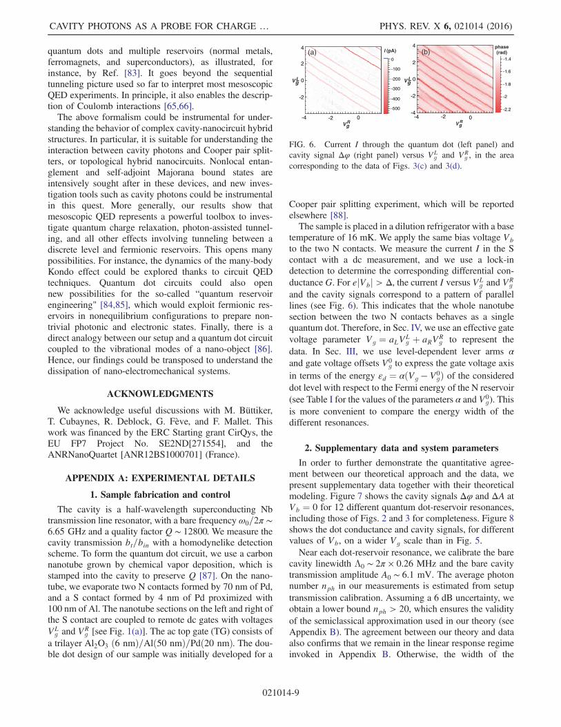
temperature of 16 mK. We apply the same bias voltage Vbto the two N contacts. We measure the current I in the Scontact with a dc measurement, and we use a lock-indetection to determine the corresponding differential con-ductance G. For ejVbj > Δ, the current I versus VL
g and VRg
and the cavity signals correspond to a pattern of parallellines (see Fig. 6). This indicates that the whole nanotubesection between the two N contacts behaves as a singlequantum dot. Therefore, in Sec. IV, we use an effective gatevoltage parameter Vg ¼ aLVL
g þ aRVRg to represent the
data. In Sec. III, we use level-dependent lever arms αand gate voltage offsets V0
g to express the gate voltage axisin terms of the energy εd ¼ αðVg − V0
gÞ of the considereddot level with respect to the Fermi energy of the N reservoir(see Table I for the values of the parameters α and V0
g). Thisis more convenient to compare the energy width of thedifferent resonances.
2. Supplementary data and system parameters
In order to further demonstrate the quantitative agree-ment between our theoretical approach and the data, wepresent supplementary data together with their theoreticalmodeling. Figure 7 shows the cavity signals Δφ and ΔA atVb ¼ 0 for 12 different quantum dot-reservoir resonances,including those of Figs. 2 and 3 for completeness. Figure 8shows the dot conductance and cavity signals, for differentvalues of Vb, on a wider Vg scale than in Fig. 5.Near each dot-reservoir resonance, we calibrate the bare
cavity linewidth Λ0 ∼ 2π × 0.26 MHz and the bare cavitytransmission amplitude A0 ∼ 6.1 mV. The average photonnumber nph in our measurements is estimated from setuptransmission calibration. Assuming a 6 dB uncertainty, weobtain a lower bound nph > 20, which ensures the validityof the semiclassical approximation used in our theory (seeAppendix B). The agreement between our theory and dataalso confirms that we remain in the linear response regimeinvoked in Appendix B. Otherwise, the width of the
-2
0
2
-4 -2-4
-2.2
-2
-1.8
-1.6
-1.4
V Rg
-500
-400
-300
-200
-100
0
-2
0
2
4
-4 -2 0 0
VLg VL
g
V Rg
I (pA)phase (rad)(a) (b)
4
FIG. 6. Current I through the quantum dot (left panel) andcavity signal Δφ (right panel) versus VL
g and VRg , in the area
corresponding to the data of Figs. 3(c) and 3(d).
CAVITY PHOTONS AS A PROBE FOR CHARGE … PHYS. REV. X 6, 021014 (2016)
021014-9

resonances in the cavity response would not match with thetheory [89].The parameters V0
g, α, ΓN , and g for the 12 resonancespresented in Figs. 2 and 7 are given in the bottom tableof Fig. 7. The dot-photon coupling g varies from2π × 55 MHz to 2π × 120 MHz and the tunnel rate ΓNfrom 2π × 0.9 GHz to 2π × 120 GHz. The circuit param-eters may take different values for different measurementshots, probably due to charge reorganizations in the sample,which change the offset V0
g or the potential landscape ofthe quantum dot. Therefore, we have separated Table I intodifferent blocks that correspond to single-shot measure-ments of a given gate voltage range. The tunnel rate ΓNdoes not show a monotonic dependence with Vg on a largescale. Sometimes, we find a locally monotonic dependence,on a scale of about 3 consecutive resonances, as illustrated
by the blocks corresponding to measurements 3 and 6 in theTable I. The nonmonotonic behavior of ΓN with Vg is verycommon in carbon nanotubes and may be attributed toweak disorder. Moreover, the variations of ΓN and g do notseem correlated, probably because ΓN depends on theproperties of the dot interfaces whereas g depends onthe overlap of the whole dot orbital with the cavity photonicpseudopotential [5]. Finally, the value of α for the meas-urement 1 differs significantly from the values used in theother measurements because aL ¼ 1 and aL ¼ 0 were usedfor measurement 1 whereas aL ¼ 0.75 and aR ¼ 0.66 wereused for the other measurements. In Sec. IV, we have used,in the theory, εd ¼ αðVg − V0
gÞ þ γVb with V0g ¼ 0.79 V,
α ¼ 2π × 723 GHz:V−1 and γ ¼ 2π × 87.3 GHz:mV−1.Since we are in the regime ΓN ≫ ΓS, we could expect
that, for each dot orbital considered in Sec. III, a fit of
TABLE I. Parameters corresponding to the different N-dot resonances shown in Fig. 7. We first show the effective gate voltage V0g and
the lever arm α extracted from the experimental data, and the fitting parameters ΓN and g used to model the cavity signals Δφ and ΔA.We also show, when possible, the value of the N-dot tunnel rate fΓN estimated from the conductance data through the S-dot-N structurefor a voltage ~Vb > Δ=e. Each block in the table corresponds to the one shot measurement of a given gate voltage range. The signals Δφ,ΔA, and G were measured simultaneously in each measurement shot.
Measurement shot 1 1 2 3 3 3 4 5 6 6 6 6
V0g (V) −0.88 0.09 0.67 −1.30 −0.65 0.47 0.75 1.16 −2.03 −1.41 −0.72 −0.16
α=2π (GHz:V−1) 200 200 667 629 629 629 657 765 704 704 704 704g=2π (MHz) 69 61 55 100 83 60 66 70 68 120 85 90ΓN=ω0 2.86 2.33 0.16 1.35 1.23 0.14 0.57 0.38 0.45 0.24 14.3 18.1ΓN=2π (GHz) 19 15.5 1.05 9.00 8.20 0.9 3.8 2.5 3 1.6 95 120fΓN=2π (GHz) 21 16 × 12.5 7.5 × × × × × 64 149~Vb (mV) −0.18 −0.37 × 0.42 0.32 × × × × × 0.24 0.24
-30 0 300.0
0.4
0.8
εd /2π (GHz)
ΓN /ω0= /2π=100MHz
-20 0 200.0
0.2
0.4
ΓN /ω0= /2π=69MHz
εd /2π (GHz)-30 0 30
0.0
0.3
0.6
ΓN /ω0= /2π=83MHz
εd /2π (GHz)-50 0 50
0.0
0.2
0.4
ΓN /ω0= /2π=61MHz
εd /2π (GHz)
Figs. 2(b),3(c)
Fig.3(d) Fig.2(c)
- ΔA/A0, exp. - ΔA/A0, theory- Δϕ, exp. (rad) - Δϕ, theory (rad)
-20 0 20
-0.1
0.0
0.1
0.2
ΓN /ω0= /2π=55MHz
εd /2π (GHz)-10 0 10
-0.1
0.0
0.1
0.2
ΓN /ω0= /2π=60MHz
εd /2π (GHz)-20 0 20
0.2
0.4
ΓN /ω0= /2π=66MHz
εd /2π (GHz)
0.0
-100 0 1000.0
0.1
0.2
0.3
εd /2π (GHz)
ΓN /ω0= /2π=90MHz
-20 0 20
0.0
0.3
0.6ΓN /ω0= /2π=70MHz
εd /2π (GHz)-20 0 20
0.2
0.4
εd /2π (GHz)
0.0
ΓN /ω0= /2π=68MHz
cavi
ty s
igna
ls
-20 0 20-0.3
0.0
0.3
0.6
ΓN /ω0= /2π=120MHz
εd /2π (GHz)
cavi
ty s
igna
ls
Fig.2(a)
Figs. 2(d),3(a)
0.0
0.2
0.4
-100 0 100
ΓN /ω0= 1.35, g2.86, g 1.23, g2.33, g
0.16, g 0.14, g0.57, g
18.1, g
0.38, g0.45, g 0.24, g
14.3, g/2π=85MHz
εd /2π (GHz)
FIG. 7. Cavity signalsΔφ (blue dots) andΔA=A0 (red dots) versus εd for Vb ¼ 0 and different dot orbitals with decreasing tunnel ratesΓN from top to bottom and left to right panels. The red and blue lines show the predictions given by Eqs. (5) and (6) for the values of ΓNand g given in the different panels and T ¼ 60 mK. When a dot-reservoir resonance is already shown in the main text, we indicate thecorresponding figure number in pink.
L. E. BRUHAT et al. PHYS. REV. X 6, 021014 (2016)
021014-10
the N-dot conductance peak for a bias voltage ~Vb > Δ=eshould give the value of the N-dot tunnel rate. Then, theonly remaining fitting parameter for Δφ and ΔA should beg. Indeed, for the 6 upper resonances in Fig. 7, a Lorentzianfit of the N-dot conductance peak gives an estimate fΓN ofthe N-dot tunnel rate, which is in rather good agreementwith the value ΓN estimated from the cavity signals (seevalues in Table I). For the highest tunnel rates ΓN=ω0 ¼18.1 and ΓN=ω0 ¼ 14.3, inaccuracies in the estimation of~ΓN stem from cotunneling peaks that appear between theCoulomb diamonds and would require a more completetheory. The conductance data for intermediate tunnel rates1.23 < ΓN=ω0 < 2.86 are more affected by experimentalnoise. One can try to minimize these two difficulties byestimating fΓN for values ~Vb of the bias voltage such that
cotunneling and experimental noise are reduced. However,for smaller tunnel rates comparable to the temperature, thestraightforward estimation of the N-dot tunnel rate from Gis not possible anymore because of temperature broadeningeffects. Therefore, in Sec. III, we preferred to treat ΓNas a fitting parameter for the cavity response, knowingthat since we have to simultaneously fit two 1D curves withtwo parameters ΓN and g, these parameters are stronglyconstrained anyway.
APPENDIX B: THEORETICAL APPROACH
1. Hamiltonian of the quantum dot circuit
To model the behavior of our setup, we use the totalHamiltonian (1) of the main text, with
Hd¼Xσ
εdd†σdσþΔ
Xk
ðcS†k↑cS†−k↓þH:c:Þ
þX
O∈fS;Ng;k;σðεOk cO†
kσ cOkσþðtOd†σ cOkσþH:c:ÞÞ
þXk;k0;σ
ðεnkk0 bn†kk0σbnkk0σþðtnbn†kk0σ cSkσþH:c:ÞÞ; ðB1Þ
the Hamiltonian of a single quantum dot contacted to a Nand a S contact. Above d†σ [c
O†kσ ] is the creation operator for
an electron with spin σ in the orbital with energy ϵd [ϵOk ] ofthe dot [reservoir O ∈ fS;Ng]. To account for the broad-ening of the BCS peaks in the density of states of S, we usean auxiliary reservoir n whose states can be populated bythe operators bn†kk0σ . For simplicity, each level kσ of S iscoupled to an independent set kk0σ of levels in n. Weassume that a bias voltage Vb is applied to the N contact,whereas the S contact is grounded. For simplicity, wedisregard Coulomb interactions in this appendix.Throughout this paper, we use ℏ ¼ 1 and define thequantities ΓN , ΓS, Γn, εd, ω0, ωrf , Δω0, ΔΛ0, and g aspulsations.
2. Calculation of the cavity microwave transmission
The two-port transmission of the cavity can be calculatedwith the input-output formalism for microwave cavities[90]. In this framework, the bosonic modes q in Eq. (1)include propagating modes in the L and R ports of thecavity, and extra modes accounting for internal cavitydamping. The L and R ports cause contributions ΛLðRÞto the bare cavity linewidth Λ0, related to the fQ couplingfactors and the mode density (see Ref. [90] for details).One can explicitly treat the excitation with frequency ωrfimposed on the cavity through the incoming mode Q of theL port (ωrf ¼ ωQ), by adding to the Hamiltonian (1) thecontribution
Hrf ¼ −iðfQa†BQe−iωrfðt−t0Þ − f�QaB�Qe
iωrfðt−t0ÞÞ; ðB2Þ
Vg (V)
-0.2
0
0.2
Vb
(mV
)
0.7
A (
mV
)
0.4
0.9
6
5
4
3
(c)(b)(a)
Δ ϕ(r
ad)
A (m
V)
4
5
6
G (e
/h)
2
0.00
0.04
Vg (V) Vg (V) Vg (V)
Vb = 0.250 mV Vb = 0.303 mV Vb = 0.336 mV
-0.1
0.1
0.2
0.0
0.80 0.86 0.80 0.86 0.80 0.86
(c)(b)(a)
FIG. 8. Top panel: Measured amplitude A versus Vb and Vg,already shown in Fig. 4(c). Bottom panels: Measured conduct-ance G (black dots), and cavity signals Δφ (blue dots) and A (reddots) versus Vg, along the dashed lines in the top panel, forVb ¼ 0.25, 0.303, and 0.336 mV from left to right. The solid red,blue, and black lines show the predictions given by Eqs. (3), (6),and (B17), for the same parameters as in Fig. 4. The areas in thegray rectangles are enlarged in Fig. 5 of the main text.
CAVITY PHOTONS AS A PROBE FOR CHARGE … PHYS. REV. X 6, 021014 (2016)
021014-11

with t0 < t an initial time before the interaction of thepropagating modes with the cavity. The term Hrf corre-sponds to a classical input signal
bin ¼ BQfQe−iωrf ðt−t0Þ=ffiffiffiffiffiffiffiffiffi2ΛL
pðB3Þ
in port L. Disregarding quantum fluctuations in the inputmodes of the cavity, Eqs. (1) and (B2) lead to
ddt
a ¼ −iω0a − ign − Λ0a − ffiffiffiffiffiffiffiffiffi2ΛL
pbin; ðB4Þ
with nðtÞ ¼ Pσd
†σdσ, while the cavity output signal is
written as
bt ¼ffiffiffiffiffiffiffiffiffi2ΛR
pa: ðB5Þ
If the number of photons in the cavity is larger than about10, we can use the semiclassical approximation a≃ hai. Inthe linear response limit and stationary regime, hai has anegligible component in eiωrf t, provided the loaded qualityfactor of the cavity remains good and ωrf ∼ ω0. In theframework of Eq. (B1), one can thus estimate the timevariations of the average number of electrons in the dotfrom the linear response to a≃ ae−iωrf t, as
hniðtÞ ¼ g~χðωrfÞae−iωrf t þ g~χð−ωrfÞa�eiωrf t: ðB6ÞThis expression involves the dot charge susceptibility
~χðtÞ ¼ −iθðtÞhfnðtÞ; nðt ¼ 0Þgig¼0 ðB7Þ
calculated in the absence of the cavity. Throughout thisappendix, we use the quantum mechanics conventionfor the Fourier transform, i.e., ~χðωÞ ¼ Rþ∞−∞ dt~χðtÞeiωt.Injecting Eq. (B6) into the statistical average of Eq. (B4)and disregarding nonresonant terms, we obtain
a ¼ −ifQBQeiωrf t0
ℏωrf − ℏω0 þ iΛ0 − g2 ~χðω0Þ: ðB8Þ
For an agreement with the experimental data, one has tokeep in mind that microwave equipment uses the electricalengineering Fourier transform convention, which is com-plex conjugated to the usual quantum mechanics conven-tion. Hence, combining Eqs. (B3), (B5), and (B8) withbt ¼ hbti and making the substitution i → −i, we obtainEq. (2) of the main text, with χðωÞ ¼ ~χðωÞ�. Note thatRefs. [5,34–36] presented related linear responseapproaches to express the cavity behavior in terms ofthe charge susceptibility of the quantum dot.
3. Keldysh description of the quantum dot circuit
Using the time-dependent Keldysh formalism [91], weobtain the expression (3) of the main text for the dot charge
susceptibility. Interestingly, Refs. [25] and [35] introducedrelated expressions, restricted to the N-dot and Andreevmolecular cases, respectively. Equation (3) involves theretarded, advanced, and lesser Green’s functions Gc of thequantum dot, with c ¼ r, a, and <, respectively, whichhave the structure
Gc ¼"Gcd↑;d
†↑
Gcd↑;d↓
Gcd†↓;d
†↑
Gcd†↓;d
c↓
#ðB9Þ
in Nambu space. For any operators A and B,we use Gr
A;BðtÞ ¼ −iθðtÞhfAðtÞ; Bðt ¼ 0Þgi and G<A;BðtÞ ¼
ihBðt ¼ 0ÞAðtÞi. From Hamiltonian (B1), one obtains[52,92]
GrðωÞ ¼ ðGaðωÞÞ† ¼ ½ω1 − Edot − ΣrðωÞ�−1; ðB10Þ
G<ðωÞ ¼ GrðωÞΣ<ðωÞGaðωÞ; ðB11Þ
with
ΣrðωÞ ¼ −iðΓN=2Þ1 − iðΓS=2ÞCðωÞ; ðB12Þ
Σ<ðωÞ ¼ iΓNfNðωÞ þ iΓSfðωÞRe½CðωÞ�: ðB13Þ
Above, we have introduced the diagonal matrices1 ¼ diagð1; 1Þ, Edot ¼ diagðεd;−εdÞ, and fNðωÞ ¼diagðfðω − eVbÞ; fðωþ eVbÞÞ. The terms ΣcðωÞ, withc ∈ fr; a; <g, describe the effect of the N and S reservoirson the quantum dot Green’s functions in the large band-width approximation. We use tunnel rates Γr ¼ 2πjtrj2ρr,with ρr the density of states per spin direction in reservoirr ∈ fS;N; ng. For describing electronic correlations in thesuperconducting reservoir, we use
CðωÞ ¼�Gω Fω
Fω Gω
�; ðB14Þ
with Gω ¼ −i½ωþ iðΓn=2Þ�=Dω, Fω ¼ iΔ=Dω, and
Dω ¼ffiffiffiffiffiffiffiffiffiffiffiffiffiffiffiffiffiffiffiffiffiffiffiffiffiffiffiffiffiffiffiffiffiffiffiffiffiΔ2 −
�ωþ i
Γn
2
�2
s: ðB15Þ
The parameter Γn is often omitted (see, for instance,Refs. [50–53,56,92,93]), but it is essential to account forthe broadening of the BCS peaks that is observedexperimentally.In the case Vb ¼ 0 and ΓS ≪ ΓN , Δ, the effect of the
superconducting contact can be disregarded, i.e., ΓS ¼ 0.In this limit, Eq. (3) leads to
L. E. BRUHAT et al. PHYS. REV. X 6, 021014 (2016)
021014-12
χðωÞ ¼ ΓN
πωðiΓN − ωÞLog�
4ϵ2d þ Γ2N
4ϵ2d − ð2ω − iΓNÞ2�
ðB16Þ
for T ¼ 0 and Eq. (5) for finite T. In the case ΓS ≠ 0,we evaluate χðωÞ numerically from Eqs. (3), (4), and(B9)–(B15).For completeness, we mention that the dc current
through the spin-degenerate quantum dot can be calculatedfor g ¼ 0 as [92]
I ¼ 2eΓNΓS
h
Zdωðfðω − eVbÞ − fðωÞÞ½GrRe½C�Ga�11
þ 2eΓ2N
h
Zdωðfðω − eVbÞ − fðωþ eVbÞÞjGr
12j2:
ðB17Þ
This expression includes quasiparticle tunneling as well asAndreev processes. With our noninteracting approach,when ΓS increases, subgap Andreev processes appearmuch more quickly than what is expected in Coulombblockade regime because Coulomb interactions forbid 2echarge fluctuations necessary for Andreev reflections[93]. In our case, this is not a problem because we havea low ΓS. In Fig. 4(b), the onset of the noninteractingAndreev current is slightly visible, but this current isbarely above the noise level of the data in the top-leftpanel. For values of ΓS larger than in our experiment, itwould be necessary to use an interacting theory tosatisfactorily reproduce the data.
4. Keldysh description of the multisite case
One can generalize the approach of Appendixes B 2and B 3 to geometries with several quantum dots or sites orseveral orbitals, denoted with an index i. In the case whereeach discrete level i ∈ ½1; N� of the nanocircuit is shifted bythe cavity field aþ a† with a constant gi, a semiclassicallinear-response description leads to Eqs. (10), (11), and(12) of the main text. These equations involve generalizedadvanced and retarded Green’s functions Ga=rðωÞ, whichencloseN × N site/orbital sub-blocks. The element Ga=r
ij ðωÞhas a Nambu structure:
Ga=rij ¼
"Ga=rdi↑;d
†j↑
Ga=rdi↑;dj↓
Ga=rd†i↓;d
†j↑
Gcd†i↓;d
cj↓
#; ðB18Þ
with Ga=rA;B scalar Green’s functions defined in Appendix B,
and Σ< the lesser self-energy of the discrete levels. Aboved†iσ is the creation operator for an electron with spin σ in theorbital level i. The matrix τi is a diagonal matrix thatcorresponds to τ in the orbital block ði; iÞ and is zerootherwise.
Note that our formalism assumes that the cavity electricfield only shifts the discrete energy levels i. This can beobtained by using ac top gates to reinforce the couplingbetween cavity photons and the quantum dot. If one uses adifferent fabrication technology with, e.g., remote ac gates,it may be necessary to assume that the cavity field alsoshifts, by a different amount, the potentials of the differentreservoirs coupled to the dot. In such a case, one can obtainsupplementary effects such as a direct influence of thequantum dot circuit conductance on the cavity linewidthshift [3,33,36,94]. A modulation of tunnel couplings by thephotonic fields could also be relevant for very high tunnelrates [5]. These cases are beyond the scope of the presentarticle.
[1] A. Wallraff, D. I. Schuster, A. Blais, L. Frunzio, R.-S.Huang, J. Majer, S. Kumar, S. M. Girvin, and R. J.Schoelkopf, Strong Coupling of a Single Photon to aSuperconducting Qubit Using Circuit Quantum Electrody-namics, Nature (London) 431, 162 (2004).
[2] L. Childress, A. S. Sørensen, and M. D. Lukin, MesoscopicCavity Quantum Electrodynamics with Quantum Dots,Phys. Rev. A 69, 042302 (2004).
[3] M. R. Delbecq, V. Schmitt, F. D. Parmentier, N. Roch, J. J.Viennot, G. Fève, B. Huard, C. Mora, A. Cottet, and T.Kontos, Coupling a Quantum Dot, Fermionic Leads, and aMicrowave Cavity on a Chip, Phys. Rev. Lett. 107, 256804(2011).
[4] T. Frey, P. J. Leek, M. Beck, A. Blais, T. Ihn, K. Ensslin, andA. Wallraff, Dipole Coupling of a Double Quantum Dot to aMicrowave Resonator, Phys. Rev. Lett. 108, 046807 (2012).
[5] A. Cottet, T. Kontos, and B. Douçot, Electron-PhotonCoupling in Mesoscopic Quantum Electrodynamics, Phys.Rev. B 91, 205417 (2015).
[6] K. D. Petersson, L.W. McFaul, M. D. Schroer, M. Jung, J.M.Taylor, A. A. Houck, and J. R. Petta, Circuit QuantumElectrodynamics with a Spin Qubit, Nature (London) 490,380 (2012).
[7] M. D. Schroer, M. Jung, K. D. Petersson, and J. R. Petta,Radio Frequency Charge Parity Meter, Phys. Rev. Lett.109, 166804 (2012).
[8] T. Frey, P. J. Leek, M. Beck, J. Faist, A. Wallraff, K. Ensslin,T. Ihn, and M. Büttiker,Quantum Dot Admittance Probed atMicrowave Frequencies with an On-Chip Resonator, Phys.Rev. B 86, 115303 (2012).
[9] H. Toida, T. Nakajima, and S. Komiyama, Vacuum RabiSplitting in a Semiconductor Circuit QED System, Phys.Rev. Lett. 110, 066802 (2013).
[10] J. Basset, D.-D. Jarausch, A. Stockklauser, T. Frey, C.Reichl, W. Wegscheider, T. M. Ihn, K. Ensslin, and A.Wallraff, Single-Electron Double Quantum Dot Dipole-Coupled to a Single Photonic Mode, Phys. Rev. B 88,125312 (2013).
[11] M.-L. Zhang, D. Wei, G.-W. Deng, S.-X. Li, H.-O. Li, G.Cao, T. Tu, M. Xiao, G.-C. Guo, H.-W. Jiang, and G.-P.Guo, Measuring the Complex Admittance of a Nearly
CAVITY PHOTONS AS A PROBE FOR CHARGE … PHYS. REV. X 6, 021014 (2016)
021014-13
Isolated Graphene Quantum Dot, Appl. Phys. Lett. 105,073510 (2014).
[12] J. J. Viennot, M. R. Delbecq, M. C. Dartiailh, A. Cottet, andT. Kontos, Out-of-Equilibrium Charge Dynamics in aHybrid Circuit Quantum Electrodynamics Architecture,Phys. Rev. B 89, 165404 (2014).
[13] Y. Y. Liu, K. D. Petersson, J. Stehlik, J. M. Taylor, and J. R.Petta, Photon Emission from a Cavity-Coupled DoubleQuantum Dot, Phys. Rev. Lett. 113, 036801 (2014).
[14] Y.-Y. Liu, J. Stehlik, C. Eichler, M. J. Gullans, J. M. Taylor,and J. R. Petta, Semiconductor Double Quantum DotMicromaser, Science 347, 285 (2015).
[15] A. Stockklauser, V. F. Maisi, J. Basset, K. Cujia, C. Reichl,W. Wegscheider, T. Ihn, A. Wallraff, and K. Ensslin, Micro-wave Emission from Hybridized States in a SemiconductorCharge Qubit, Phys. Rev. Lett. 115, 046802 (2015).
[16] Y.-Y. Liu, J. Stehlik, M. J. Gullans, J. M. Taylor, and J. R.Petta, Injection Locking of a Semiconductor Double Quan-tum Dot Micromaser, Phys. Rev. A 92, 053802 (2015).
[17] J. J. Viennot, M. C. Dartiailh, A. Cottet, and T. Kontos,Coherent Coupling of a Single Spin to Microwave CavityPhotons, Science 349, 408 (2015).
[18] A. Cottet, T. Kontos, S. Sahoo, H. T. Man, M.-S. Choi, W.Belzig, C. Bruder, A. F. Morpurgo, and C. Schönenberger,Nanospintronics with Carbon Nanotubes, Semicond. Sci.Technol. 21, S78 (2006).
[19] L. Hofstetter, S. Csonka, J. Nygard, and C. Schönenberger,Cooper Pair Splitter Realized in a Two-Quantum-DotY-Junction, Nature (London) 461, 960 (2009).
[20] L. G. Herrmann, F. Portier, P. Roche, A. L. Yeyati, T. Kontos,and C. Strunk, Carbon Nanotubes as Cooper-Pair BeamSplitters, Phys. Rev. Lett. 104, 026801 (2010).
[21] J.-D. Pillet, C. Quay, P. Morfin, C. Bena, A. Levy Yeyati,and P. Joyez, Andreev Bound States in Supercurrent-Carrying Carbon Nanotubes Revealed, Nat. Phys. 6, 965(2010).
[22] T. Dirks, T. L. Hughes, S. Lal, B. Uchoa, Y.-F. Chen, C.Chialvo, P. M. Goldbart, and N. Mason, Transport throughAndreev Bound States in a Graphene Quantum Dot, Nat.Phys. 7, 386 (2011).
[23] C. Janvier, L. Tosi, L. Bretheau, Ç. Ö. Girit, M. Stern, P.Bertet, P. Joyez, D. Vion, D. Esteve, M. F. Goffman, H.Pothier, and C. Urbina, Coherent Manipulation of AndreevStates in Superconducting Atomic Contacts, Science 349,1199 (2015).
[24] V. Mourik, K. Zuo, S. M. Frolov, S. R. Plissard, E. P. A. M.Bakkers, and L. P. Kouwenhoven, Signatures of MajoranaFermions in Hybrid Superconductor-SemiconductorNanowire Devices, Science 336, 1003 (2012).
[25] J. Sköldberg, T. Löfwander, V. S. Shumeiko, and M.Fogelström, Spectrum of Andreev Bound States in aMolecule Embedded Inside a Microwave-Excited Super-conducting Junction, Phys. Rev. Lett. 101, 087002 (2008).
[26] A. Cottet, T. Kontos, and A. Levy Yeyati, Subradiant SplitCooper Pairs, Phys. Rev. Lett. 108, 166803 (2012).
[27] A. Cottet, Probing Coherent Cooper Pair Splitting withCavity Photons, Phys. Rev. B 90, 125139 (2014).
[28] M. Trif and Y. Tserkovnyak, Resonantly Tunable MajoranaPolariton in a Microwave Cavity, Phys. Rev. Lett. 109,257002 (2012).
[29] T. L. Schmidt, A. Nunnenkamp, and C. Bruder, MajoranaQubit Rotations in Microwave Cavities, Phys. Rev. Lett.110, 107006 (2013).
[30] A. Cottet, T. Kontos, and B. Douçot, Squeezing Light withMajorana Fermions, Phys. Rev. B 88, 195415 (2013).
[31] O. Dmytruk, M. Trif, and P. Simon, Cavity QuantumElectrodynamics with Mesoscopic Topological Supercon-ductors, Phys. Rev. B 92, 245432 (2015).
[32] R. Chirla, A. Manolescu, and C. P. Moca, Transmission of aMicrowave Cavity Coupled to Localized Shiba States, Phys.Rev. B 93, 155110 (2016).
[33] M. R. Delbecq, L. E. Bruhat, J. J. Viennot, S. Datta, A.Cottet, and T. Kontos, Photon-Mediated Interactionbetween Distant Quantum Dot Circuits, Nat. Commun. 4,1400 (2013).
[34] A. Cottet, C. Mora, and T. Kontos, Mesoscopic Admittanceof a Double Quantum Dot, Phys. Rev. B 83, 121311(R)(2011).
[35] M. Schiró and K. Le Hur, Tunable Hybrid QuantumElectrodynamics from Nonlinear Electron Transport, Phys.Rev. B 89, 195127 (2014).
[36] O. Dmytruk, M. Trif, C. Mora, and P. Simon, CavityQuantum Electrodynamics with an Out-of-EquilibriumQuantum Dot, Phys. Rev. B 93, 075425 (2016).
[37] M. Büttiker, H. Thomas, and A. Prêtre, MesoscopicCapacitors, Phys. Lett. A 180, 364 (1993).
[38] A. Prêtre, H. Thomas, and M. Büttiker, Dynamic Admit-tance of Mesoscopic Conductors: Discrete-Potential Model,Phys. Rev. B 54, 8130 (1996).
[39] J. Gabelli, G. Fève, J.-M. Berroir, B. Plaçais, A. Cavanna, B.Etienne, Y. Jin, and D. C. Glattli, Violation of Kirchhoff’sLaws for a Coherent RC Circuit, Science 313, 499 (2006).
[40] G. Fève, A. Mahé, J.-M. Berroir, T. Kontos, B. Plaçais, C.Glattli, A. Cavanna, B. Etienne, and Y. Jin, An On-DemandCoherent Single Electron Source, Science 316, 1169 (2007).
[41] S. Nigg, R. Lopez, and M. Büttiker, Mesoscopic ChargeRelaxation, Phys. Rev. Lett. 97, 206804 (2006).
[42] Ya. I. Rodionov, I. S. Burmistrov, and A. S. Ioselevich,Charge Relaxation Resistance in the Coulomb BlockadeProblem, Phys. Rev. B 80, 035332 (2009).
[43] C. Mora and K. Le Hur, Universal Resistances of theQuantum RC Circuit, Nat. Phys. 6, 697 (2010).
[44] Y. Hamamoto, T. Jonckheere, T. Kato, and T. Martin,Dynamic Response of a Mesoscopic Capacitor in thePresence of Strong Electron Interactions, Phys. Rev. B81, 153305 (2010).
[45] M. Filippone, K. Le Hur, and C. Mora, Giant ChargeRelaxation Resistance in the Anderson Model, Phys. Rev.Lett. 107, 176601 (2011).
[46] M. Lee, R. Lopez, M.-S. Choi, T. Jonckheere, and T. Martin,Many-Body Correlation Effect on Mesoscopic ChargeRelaxation, Phys. Rev. B 83, 201304 (2011).
[47] I. S. Burmistrov and Ya. I. Rodionov, Charge RelaxationResistance in the Cotunneling Regime of Multi-ChannelCoulomb Blockade: Violation of Korringa-Shiba Relation,Phys. Rev. B 92, 195412 (2015).
[48] T. W. Larsen, K. D. Petersson, F. Kuemmeth, T. S. Jespersen,P. Krogstrup, J. Nygard, and C. M.Marcus,A SemiconductorNanowire-Based Superconducting Qubit, Phys. Rev. Lett.115, 127001 (2015).
L. E. BRUHAT et al. PHYS. REV. X 6, 021014 (2016)
021014-14
[49] G. de Lange, B. van Heck, A. Bruno, D. J. vanWoerkom, A.Geresdi, S. R. Plissard, E. P. A. M. Bakkers, A. R.Akhmerov, and L. DiCarlo, Realization of MicrowaveQuantum Circuits Using Hybrid Superconducting-Semiconducting Nanowire Josephson Elements, Phys.Rev. Lett. 115, 127002 (2015).
[50] C. B. Whan and T. P. Orlando, Transport Properties of aQuantum Dot with Superconducting Leads, Phys. Rev. B54, R5255(R) (1996).
[51] H.-K. Zhao and G. v. Gehlen, Mesoscopic Transportthrough a Normal-Metal-Quantum-Dot-SuperconductorSystem with ac Responses, Phys. Rev. B 58, 13660 (1998).
[52] Q.-f. Sun, J. Wang, and T.-h. Lin, Photon-Assisted AndreevTunneling through a Mesoscopic Hybrid System, Phys. Rev.B 59, 13126 (1999).
[53] S. Y. Cho, K. Kang, and C.-M. Ryu, Photon-AssistedQuasiparticle Transport and Andreev Transport throughan Interacting Quantum Dot, Phys. Rev. B 60, 16874(1999).
[54] Y. Zhu, W. Li, T.-h. Lin, and Q.-f. Sun,Microwave-Inducedπ-Junction Transition in a Superconductor/QuantumDot/Superconductor Structure, Phys. Rev. B 66, 134507(2002).
[55] T. K. T. Nguyen, T. Jonckheere, A. Crépieux, A. V. Nguyen,and T. Martin, Photoassisted Andreev Reflection as a Probeof Quantum Noise, Phys. Rev. B 76, 035421 (2007).
[56] A. Nurbawono, Y. P. Feng, and C. Zhang, Electron Tunnel-ing through a Hybrid Superconducting-Normal MesoscopicJunction under Microwave Radiation, Phys. Rev. B 82,014535 (2010).
[57] A. G. Moghaddam, M. Governale, and J. König, DrivenSuperconducting Proximity Effect in Interacting QuantumDots, Phys. Rev. B 85, 094518 (2012).
[58] R. Avriller and F. Pistolesi, Andreev Bound-State Dynamicsin Quantum-Dot Josephson Junctions: A Washing Out ofthe 0-π Transition, Phys. Rev. Lett. 114, 037003 (2015).
[59] J. Baranski and T. Domanski, Enhancements of the AndreevConductance due to Emission/Absorption of BosonicQuanta, J. Phys. Condens. Matter 27, 305302 (2015).
[60] If one uses two N contacts with a similar structure and thesame bias voltage, this only increases the effective density ofstates ρN of the normal continuum seen by the quantum dot.In this picture, the effective tunnel rate ΓN ¼ 2πjtN j2ρNcorresponds to the sum of the tunnel rates of the two real Ncontacts.
[61] J. Wang, B. Wang, and H. Guo, Quantum Inductance andNegative Electrochemical Capacitance at Finite Frequencyin a Two-Plate Quantum Capacitor, Phys. Rev. B 75,155336 (2007).
[62] This mapping is valid as long as the cavity resonance iswell described by a Lorentzian, which is the case we areconcerned with [see Eq. (10)]. In particular, the prefactor t0,which characterizes our setup transmission, is assumed tobe frequency independent in the explored range, and bydefinition, it is not changed by the nanocircuit.
[63] In the linear limit where Δφ and ΔA are small, one hasΔω0 ≃ Λ0Δφ and ΔΛ0 ≃−Λ0ΔA=A0 so that Δω0 and ΔΛ0
reveal the cavity frequency and linewidth shifts, respec-tively. However, since we have strong signals, it is moreaccurate to use the nonlinear relations of the main text.
[64] H. Shiba, The Korringa Relation for the Impurity NuclearSpin Lattice Relaxation in Dilute Kondo Alloys, Prog.Theor. Phys. 54, 967 (1975).
[65] Y. Meir, N. S. Wingreen, and P. A. Lee, Transport through aStrongly Interacting Electron System: Theory of PeriodicConductance Oscillations, Phys. Rev. Lett. 66, 3048 (1991).
[66] A. Martin-Rodero, A. Levy Yeyati, F. Flores, and R. C.Monreal, Interpolative Approach for Electron and Electron-Phonon Interactions: From the Kondo to the PolaronicRegime, Phys. Rev. B 78, 235112 (2008).
[67] T. Dirks, Y.-F. Chen, N. O. Birge, and N. Mason, Super-conducting Tunneling Spectroscopy of a Carbon NanotubeQuantum Dot, Appl. Phys. Lett. 95, 192103 (2009).
[68] S. Pfaller, A. Donarini, and M. Grifoni, SubgapFeatures Due to Quasiparticle Tunneling in Quantum DotsCoupled to Superconducting Leads, Phys. Rev. B 87,155439 (2013).
[69] J. Gramich, A. Baumgartner, and C. Schönenberger,Resonantand Inelastic Andreev Tunneling Observed on a CarbonNanotube Quantum Dot, Phys. Rev. Lett. 115, 216801(2015).
[70] D. C. Ralph, C. T. Black, M. Tinkham, D. C. Ralph, C. T.Black, and M. Tinkham, Spectroscopic Measurements ofDiscrete Electronic States in Single Metal Particles, Phys.Rev. Lett. 74, 3241 (1995).
[71] P. K. Tien and J. P. Gordon, Multiphoton Process Observedin the Interaction of Microwave Fields with the Tunnelingbetween Superconductor Films, Phys. Rev. 129, 647 (1963).
[72] L. P. Kouwenhoven, S. Jauhar, J. Orenstein, P. L. McEuen,Y.Nagamune, J. Motohisa, and H. Sakaki, Observation ofPhoton-Assisted Tunneling through a Quantum Dot, Phys.Rev. Lett. 73, 3443 (1994).
[73] L. P. Kouwenhoven, S. Jauhar, K. McCormick, D.Dixon,P. L. McEuen, Yu. V. Nazarov, N. C. van der Vaart,and C. T. Foxon, Photon-Assisted Tunneling througha Quantum Dot, Phys. Rev. B 50, 2019 (1994).
[74] R. H. Blick, R. J. Haug, D. W. van der Weide, K.von Klitzing, and K. Eberl, Photon-Assisted Tunnelingthrough a Quantum Dot at High Microwave Frequencies,Appl. Phys. Lett. 67, 3924 (1995).
[75] In the semiclassical limit, by combining Eqs. (B4) and (B6)with χð−ω0Þ ¼ χðω0Þ�, one obtains a photon emission/absorption rate Γe=a ¼ −2g2Im½χðω0Þ�nph. Then, fromRef. [63], for linear cavity signals, one has ΔΛ0¼g2Im½χðω0Þ�≃−Λ0ΔA=A0. This givesΓe=a≃2nphΛ0ΔA=A0.
[76] S. DeFranceschi, L. Kouwenhoven, C. Schönenberger,and W. Wernsdorfer, Hybrid Superconductor-QuantumDot Devices, Nat. Nanotechnol. 5, 703 (2010).
[77] C. Feuillet-Palma, T. Delattre, P. Morfin, J.-M. Berroir, G.Fève, D. C. Glattli, B. Plaçais, A. Cottet, and T. Kontos,Conserved Spin and Orbital Phase along Carbon Nano-tubes Connected with Multiple Ferromagnetic Contacts,Phys. Rev. B 81, 115414 (2010).
[78] A. D. Crisan, S. Datta, J. J. Viennot, M. R. Delbecq, A.Cottet, and T. Kontos, Harnessing Spin Precession withDissipation, Nat. Commun. 7, 10451 (2016).
[79] R. Leturcq, D. Graf, T. Ihn, K. Ensslin, D. D. Driscoll, andA. C. Gossard, Multi-Terminal Transport through a Quan-tum Dot in the Coulomb-Blockade Regime, Europhys. Lett.67, 439 (2004).
CAVITY PHOTONS AS A PROBE FOR CHARGE … PHYS. REV. X 6, 021014 (2016)
021014-15
[80] As a first test, we have checked that the multisite Eq. (11)agrees with the expressions given in Ref. [34] for anoninteracting equilibrium double quantum dot with Nreservoirs.
[81] In the multidot case, we define χijðtÞ ¼ −iθðtÞhfniðtÞ;njðt ¼ 0Þgi0, where ni is the quantum operator for thenumber of electrons in site i and hi0 denotes the statisticalaveraging with gi ¼ 0 for i ∈ ½1; N�.
[82] For instance, in the case of a noninteracting single quantumdot in equilibrium with N reservoirs, Eq. (5) can berecovered from the Landauer Büttiker scattering descriptionused in Ref. [8].
[83] P. Trocha and J. Barnaś, Spin-Polarized Andreev TransportInfluenced by Coulomb Repulsion through a Two-Quantum-Dot System, Phys. Rev. B 89, 245418 (2014).
[84] A. Sarlette, J. M. Raimond, M. Brune, and P. Rouchon,Stabilization of Nonclassical States of the Radiation Field ina Cavity by Reservoir Engineering, Phys. Rev. Lett. 107,010402 (2011).
[85] E. T. Holland, B. Vlastakis, R.W. Heeres, M. J. Reagor, U.Vool, Z. Leghtas, L. Frunzio, G. Kirchmair, M. H. Devoret,M. Mirrahimi, and R. J. Schoelkopf, Single-Photon ResolvedCross-Kerr Interaction for Autonomous Stabilization ofPhoton-Number States, Phys. Rev. Lett. 115, 180501 (2015).
[86] G. A. Steele, A. K. Hüttel, B. Witkamp, M. Poot, H. B.Meerwaldt, L. P. Kouwenhoven, and H. S. J. van der Zant,
Strong Coupling between Single-Electron Tunneling andNanomechanical Motion, Science 325, 1103 (2009).
[87] J. J. Viennot, J. Palomo, and T. Kontos, Stamping SingleWall Nanotubes for Circuit Quantum Electrodynamics,Appl. Phys. Lett. 104, 113108 (2014).
[88] L. E. Bruhat et al. (in preparation).[89] To be published elsewhere.[90] A. A. Clerk, M. H. Devoret, S. M. Girvin, F. Marquardt, and
R. J. Schoelkopf, Introduction to Quantum Noise, Meas-urement and Amplification, Rev. Mod. Phys. 82, 1155(2010).
[91] A.-P. Jauho, N. S. Wingreen, and Y. Meir, Time-DependentTransport in Interacting and Noninteracting Resonant-Tunneling Systems, Phys. Rev. B 50, 5528 (1994).
[92] Qing-feng Sun, Jian Wang, and Tsung-han Lin, ResonantAndreev Reflection in a Normal-Metal-Quantum-Dot–Superconductor System, Phys. Rev. B 59, 3831 (1999).
[93] K. Kang, Multiple Andreev Reflections through anInteracting Quantum Dot, Physica (Amsterdam) 5E, 36(1999).
[94] N. Ares, F. J. Schupp, A. Mavalankar, G. Rogers, J.Griffiths, G. A. C. Jones, I. Farrer, D. A. Ritchie, C. G.Smith, A. Cottet, G. A. D. Briggs, and E. A. Laird, SensitiveRadio-Frequency Measurements of a Quantum Dot byTuning to Perfect Impedance Matching, Phys. Rev. Applied5, 034011 (2016).
L. E. BRUHAT et al. PHYS. REV. X 6, 021014 (2016)
021014-16