Embed Size (px)
Citation preview
Cavity State Reservoir Engineering inCircuit Quantum Electrodynamics
A DissertationPresented to the Faculty of the Graduate School
ofYale University
in Candidacy for the Degree ofDoctor of Philosophy
byEric T. Holland
Dissertation Director: Robert J. Schoelkopf
August 2015

©2015 – Eric T. Hollandall rights reserved.

Thesis advisor: Professor Robert J. Schoelkopf Eric T. Holland
Cavity State Reservoir Engineering in Circuit QuantumElectrodynamics
Abstract
Engineered quantum systems are poised to revolutionize information science inthe near future. A persistent challenge in applied quantum technology is creat-ing controllable, quantum interactions while preventing information loss to theenvironment, decoherence. In this thesis, we realize mesoscopic superconductingcircuits whose macroscopic collective degrees of freedom, such as voltages andcurrents, behave quantum mechanically. We couple these mesoscopic devices tomicrowave cavities forming a cavity quantum electrodynamics (QED) architec-ture comprising entirely of circuit elements. This application of cavity QED isdubbed Circuit QED and is an interdisciplinary field seated at the intersectionof electrical engineering, superconductivity, quantum optics, and quantum infor-mation science. Two popular methods for taming active quantum systems in thepresence of decoherence are discrete feedback conditioned on an ancillary sys-tem or quantum reservoir engineering. Quantum reservoir engineering maintainsa desired quantum state through a combination of drives and designed entropyevacuation. Circuit QED provides a favorable platform for investigating quan-tum reservoir engineering proposals. A major advancement of this thesis is thedevelopment of a quantum reservoir engineering protocol which maintains thequantum state of a microwave cavity in the presence of decoherence. This thesissynthesizes of strongly coupled, coherent devices whose solutions to its driven,dissipative Hamiltonian are predicted a priori. This work lays the foundationfor future advancements in cavity centered quantum reservoir engineering pro-tocols that have potential to realize hardware efficient protocols to protect moreelaborate quantum states.
iii
Contents
List of Figures viii
List of Tables x
Publication List xi
Acknowledgements xii
1 Introduction 11.1 Thesis Overview . . . . . . . . . . . . . . . . . . . . . . . . . . . . 5
2 Resonator Theory 72.1 LC Circuit . . . . . . . . . . . . . . . . . . . . . . . . . . . . . . . 92.2 LCR Circuit . . . . . . . . . . . . . . . . . . . . . . . . . . . . . . 112.3 Quality factors . . . . . . . . . . . . . . . . . . . . . . . . . . . . 12
2.3.1 Quality Factor Parallel LCR Circuit . . . . . . . . . . . . . 132.4 Coupling to LC Oscillator . . . . . . . . . . . . . . . . . . . . . . 152.5 Participation Ratios . . . . . . . . . . . . . . . . . . . . . . . . . 18
2.5.1 Lossy Capacitor . . . . . . . . . . . . . . . . . . . . . . . . 182.5.2 Partially Filled Lossy Capacitor-Parallel . . . . . . . . . . 202.5.3 Partially Filled Lossy Capacitor-Series . . . . . . . . . . . 252.5.4 Lossy Inductor . . . . . . . . . . . . . . . . . . . . . . . . 272.5.5 Partially Filled Lossy Inductor-Series . . . . . . . . . . . . 282.5.6 Partially Filled Lossy Inductor-Parallel . . . . . . . . . . . 30
2.6 Final Thoughts . . . . . . . . . . . . . . . . . . . . . . . . . . . . 33
3 Transmission Line Resonators 343.1 Historical Development . . . . . . . . . . . . . . . . . . . . . . . . 353.2 Characteristic Impedance . . . . . . . . . . . . . . . . . . . . . . . 36
iv

3.3 Design Consideration . . . . . . . . . . . . . . . . . . . . . . . . . 383.4 First Design . . . . . . . . . . . . . . . . . . . . . . . . . . . . . . 413.5 Participation Ratios . . . . . . . . . . . . . . . . . . . . . . . . . 43
3.5.1 Surface Dielectric Loss . . . . . . . . . . . . . . . . . . . . 443.5.2 Bulk Dielectric Loss . . . . . . . . . . . . . . . . . . . . . 473.5.3 Inductive losses and Kinetic Inductance Ratio . . . . . . . 49
3.6 Evanescent Coupling . . . . . . . . . . . . . . . . . . . . . . . . . 523.6.1 Asymmetry and Coupling Through TE01 Mode . . . . . . 57
3.7 Quality Factor Measurements . . . . . . . . . . . . . . . . . . . . 583.8 Kinetic Inductance Ratio Measurements . . . . . . . . . . . . . . 613.9 Limitations . . . . . . . . . . . . . . . . . . . . . . . . . . . . . . 62
3.9.1 Coupling . . . . . . . . . . . . . . . . . . . . . . . . . . . . 643.9.2 Frequency Stability . . . . . . . . . . . . . . . . . . . . . . 643.9.3 Issue Resolution . . . . . . . . . . . . . . . . . . . . . . . . 65
3.10 Future Outlook . . . . . . . . . . . . . . . . . . . . . . . . . . . . 67
4 Circuit Quantum Electrodynamics 684.1 Cavity Quantum Electrodynamics . . . . . . . . . . . . . . . . . . 714.2 Josephson Junction as a Circuit Element . . . . . . . . . . . . . . 734.3 Circuit Quantization . . . . . . . . . . . . . . . . . . . . . . . . . 76
4.3.1 LC Oscillator . . . . . . . . . . . . . . . . . . . . . . . . . 764.3.2 Anharmonic Oscillator: The Transmon . . . . . . . . . . . 77
4.4 Transmon Coupled to Harmonic Oscillator . . . . . . . . . . . . . 794.4.1 Strong Dispersive Regime . . . . . . . . . . . . . . . . . . 82
4.5 Black box quantization . . . . . . . . . . . . . . . . . . . . . . . . 84
5 Experimental Techniques 895.1 Fabrication . . . . . . . . . . . . . . . . . . . . . . . . . . . . . . 90
5.1.1 Substrates . . . . . . . . . . . . . . . . . . . . . . . . . . . 905.1.2 Lithography . . . . . . . . . . . . . . . . . . . . . . . . . . 915.1.3 Deposition and Dicing . . . . . . . . . . . . . . . . . . . . 94
5.2 Sample Holders . . . . . . . . . . . . . . . . . . . . . . . . . . . . 955.2.1 Striplines . . . . . . . . . . . . . . . . . . . . . . . . . . . 955.2.2 Cavities . . . . . . . . . . . . . . . . . . . . . . . . . . . . 96
5.3 Experimental Setup . . . . . . . . . . . . . . . . . . . . . . . . . . 965.3.1 Dilution Refrigerator . . . . . . . . . . . . . . . . . . . . . 965.3.2 Vericold Wiring and Filtering . . . . . . . . . . . . . . . . 975.3.3 Cavity Filtering . . . . . . . . . . . . . . . . . . . . . . . . 97
v

5.3.4 Heterodyne Measurement Setup . . . . . . . . . . . . . . . 1015.4 Cavity Measurement Techniques . . . . . . . . . . . . . . . . . . . 103
5.4.1 Transmission . . . . . . . . . . . . . . . . . . . . . . . . . 1035.5 Qubit Measurement Techniques . . . . . . . . . . . . . . . . . . . 105
5.5.1 Dispersive Readout . . . . . . . . . . . . . . . . . . . . . . 1075.5.2 Jaynes-Cummings Readout . . . . . . . . . . . . . . . . . 108
6 Cavity State Reservoir Engineering 1116.1 Introduction . . . . . . . . . . . . . . . . . . . . . . . . . . . . . . 111
6.1.1 Measurement with External Feedback . . . . . . . . . . . . 1126.1.2 Quantum Reservoir Engineering . . . . . . . . . . . . . . . 116
6.2 Fock State Stabilization Protocol . . . . . . . . . . . . . . . . . . 1186.2.1 Four State Model . . . . . . . . . . . . . . . . . . . . . . . 121
6.3 Linblad Master Equation and Simulation . . . . . . . . . . . . . . 1246.4 Photon Number Calibration via the AC stark effect . . . . . . . . 1256.5 Hamiltonian Parameters . . . . . . . . . . . . . . . . . . . . . . . 129
6.5.1 Anharmonicities . . . . . . . . . . . . . . . . . . . . . . . . 1316.5.2 Cavity-Cavity Cross-Kerr . . . . . . . . . . . . . . . . . . 133
6.6 Photon Number Selective π Pulse Calibration . . . . . . . . . . . 1356.6.1 π Pulse Selectivity . . . . . . . . . . . . . . . . . . . . . . 137
6.7 Fock State Stabilization Protocol . . . . . . . . . . . . . . . . . . 1376.7.1 Comparison DDROP and FSSP . . . . . . . . . . . . . . . 1406.7.2 Steady State Wigner Function for Stabilized N=1 Fock State1426.7.3 Interpreting Results as a Spin System . . . . . . . . . . . . 144
6.8 Future Improvements . . . . . . . . . . . . . . . . . . . . . . . . . 1476.8.1 Final Comment . . . . . . . . . . . . . . . . . . . . . . . . 151
7 Conclusion & Outlook 1527.1 Conclusion . . . . . . . . . . . . . . . . . . . . . . . . . . . . . . . 1527.2 Future Experiments . . . . . . . . . . . . . . . . . . . . . . . . . . 153
7.2.1 Extension to Fock State Stabilization . . . . . . . . . . . . 1537.2.2 N00N State Stabilization . . . . . . . . . . . . . . . . . . . 154
7.3 Future Outlook . . . . . . . . . . . . . . . . . . . . . . . . . . . . 156
Appendix A Recipes 158A.1 Cavity Photolithography . . . . . . . . . . . . . . . . . . . . . . . 158
A.1.1 Resist . . . . . . . . . . . . . . . . . . . . . . . . . . . . . 158A.1.2 Development . . . . . . . . . . . . . . . . . . . . . . . . . 159
A.2 Cavity Etching . . . . . . . . . . . . . . . . . . . . . . . . . . . . 160
vi

A.2.1 Tools Required . . . . . . . . . . . . . . . . . . . . . . . . 160A.2.2 Setting Up . . . . . . . . . . . . . . . . . . . . . . . . . . . 161A.2.3 Acid change at two hour mark . . . . . . . . . . . . . . . . 161A.2.4 Finish . . . . . . . . . . . . . . . . . . . . . . . . . . . . . 162
A.3 Dolan Bridge Josephson Junction Recipe . . . . . . . . . . . . . . 163A.3.1 Wafer Cleaning (15 minutes) . . . . . . . . . . . . . . . . . 163A.3.2 Resist spinning (45 minutes) . . . . . . . . . . . . . . . . . 164A.3.3 Anti-charging Layer (1 hour) . . . . . . . . . . . . . . . . . 164A.3.4 Electron beam writing (2-4 hours depending area to be writ-
ten) . . . . . . . . . . . . . . . . . . . . . . . . . . . . . . 165A.3.5 Development (15 minutes) . . . . . . . . . . . . . . . . . . 165A.3.6 Deposition (4 hours) . . . . . . . . . . . . . . . . . . . . . 166A.3.7 Liftoff (2+hours) . . . . . . . . . . . . . . . . . . . . . . . 166A.3.8 Dicing (4 hours) . . . . . . . . . . . . . . . . . . . . . . . . 167A.3.9 After dicing (2 hours) . . . . . . . . . . . . . . . . . . . . 167
Appendix B QuTiP Code 169B.1 Fock State Stabilization . . . . . . . . . . . . . . . . . . . . . . . 169
B.1.1 Time Dependent Solver . . . . . . . . . . . . . . . . . . . . 169B.1.2 Steady State Solver . . . . . . . . . . . . . . . . . . . . . . 173
Bibliography 189
vii

List of Figures
2.1 LC Circuit Diagram . . . . . . . . . . . . . . . . . . . . . . . . . 92.2 LCR Circuit Diagram . . . . . . . . . . . . . . . . . . . . . . . . . 112.3 Coupling to LC Oscillator . . . . . . . . . . . . . . . . . . . . . . 152.4 Lossy Capacitor . . . . . . . . . . . . . . . . . . . . . . . . . . . . 182.5 Lossy Capacitor-Partially Filled Parallel . . . . . . . . . . . . . . 212.6 Lossy Capacitor-Partially Filled Series . . . . . . . . . . . . . . . 242.7 Lossy Inductor . . . . . . . . . . . . . . . . . . . . . . . . . . . . 272.8 Lossy Inductor-Partially Filled Series . . . . . . . . . . . . . . . . 292.9 Lossy Inductor-Partially Filled Parallel . . . . . . . . . . . . . . . 31
3.1 Microstrip Tri-Plate and Stripline . . . . . . . . . . . . . . . . . . 373.2 Prototypical Stripline . . . . . . . . . . . . . . . . . . . . . . . . . 383.3 Rectangular Waveguide Cavity . . . . . . . . . . . . . . . . . . . . 403.4 Stripline First Design . . . . . . . . . . . . . . . . . . . . . . . . . 423.5 Center Conductor Surface Participation Ratio . . . . . . . . . . . 483.6 Kinetic Inductance Calculation . . . . . . . . . . . . . . . . . . . 513.7 Evanescent Coupling to 3D Cavity and Stripline . . . . . . . . . . 563.8 Total Quality Factor versus Temperature . . . . . . . . . . . . . . 593.9 Measured Kinetic Inductance of Stripline Resonator and Holder . 623.10 Stripline Second Design . . . . . . . . . . . . . . . . . . . . . . . . 633.11 Coaxline . . . . . . . . . . . . . . . . . . . . . . . . . . . . . . . . 66
4.1 Jaynes-Cummings Model . . . . . . . . . . . . . . . . . . . . . . . 704.2 CQED Realization . . . . . . . . . . . . . . . . . . . . . . . . . . 724.3 Josephson Junction Schematic and Circuit Equivalent . . . . . . . 734.4 Circuit Representation of Transmon . . . . . . . . . . . . . . . . . 784.5 Circuit Representation of Transmon Coupled to LC Oscillator . . 814.6 Charge Based Superconducting Qubits . . . . . . . . . . . . . . . 834.7 Black Box Quantization HFSS Simulation . . . . . . . . . . . . . 86
viii

5.1 Double Angle Dolan Bridge Deposition . . . . . . . . . . . . . . . 935.2 Vericold Dilution Refrigerator Wiring . . . . . . . . . . . . . . . . 985.3 Room Temperature Microwave Control and Data Acquisition . . . 1025.4 Dispersive Readout . . . . . . . . . . . . . . . . . . . . . . . . . . 1065.5 Jaynes-Cummings Readout . . . . . . . . . . . . . . . . . . . . . . 109
6.1 Conceptual schematic of reservoir engineering . . . . . . . . . . . 1166.2 Fock state stabilization protocol . . . . . . . . . . . . . . . . . . . 1206.3 Four state model . . . . . . . . . . . . . . . . . . . . . . . . . . . 1236.4 AC Stark Photon Number Calibration . . . . . . . . . . . . . . . 1266.5 AC Stark Amplitude . . . . . . . . . . . . . . . . . . . . . . . . . 1296.6 AC Stark Calibration . . . . . . . . . . . . . . . . . . . . . . . . . 1306.7 Storage Cavity Anharmonicity . . . . . . . . . . . . . . . . . . . . 1326.8 Single Photon Cross-Kerr . . . . . . . . . . . . . . . . . . . . . . 1336.9 Photon Number Poisson Distribution . . . . . . . . . . . . . . . . 1386.10 P(0) and P(1) . . . . . . . . . . . . . . . . . . . . . . . . . . . . . 1416.11 Steady State Wigner function . . . . . . . . . . . . . . . . . . . . 1456.12 Steady State Cavity Polarization . . . . . . . . . . . . . . . . . . 1486.13 Expected FSS . . . . . . . . . . . . . . . . . . . . . . . . . . . . . 150
7.1 Historical Progress of Superconducting Circuits . . . . . . . . . . 156
ix

List of Tables
6.1 Fock State Stabilization Parameters . . . . . . . . . . . . . . . . . 1356.2 Comparison FSSP and DDROP . . . . . . . . . . . . . . . . . . . 142
x

Publication List
This thesis is based on the following publications:
1. M. Reagor, W. Pfaff, C. Axline, R. W. Heeres, N. Ofek, K. Sliwa, E. T.Holland, C. Wang, J. Blumoff, K. Chou, M. J. Hatridge, L. Frunzio, M. H.Devoret, L. Jiang, and R. J. Schoelkopf. (2015)
2. E. T. Holland, B. Vlastakis, R. W. Heeres, M. J. Reagor, U. Vool, Z. Legh-tas, L. Frunzio, G. Kirchmair, M. H. Devoret, M. Mirrahimi, and R. J.Schoelkopf. (2015)
3. Reinier W. Heeres, Brian Vlastakis, Eric T. Holland, Stefan Krastanov,Victor Albert, Luigi Frunzio, Liang Jiang, and Robert J. Schoelkopf. (2015)
4. M. J. Reagor, H. Paik, G. Catelani, L. Sun, C. Axline, E. T. Holland, I.M. Pop, N. A. Masluk, T. Brecht, L. Frunzio, et al., Appl. Phys. Lett.102, 192604 (2013)
xi

Acknowledgments
First and foremost I would like to thank my advisor, Robert Schoelkopf, forthe past six years. Much of what I have learned about microwave and quantummeasurement has been through discussions with him. Furthermore, the 4th floorof Becton is a hub of innovative quantum research. Few other places can boastthe intellectual and physical resources that are available there. Next I wouldlike to thank Luigi Frunzio for his unbridled enthusiasm for science coupledwith his meticulous attention to detail. It has been a pleasure working with andlearning from Luigi over the last six years. Michel Devoret has been a seeminglynever ending source for profound pedagogical insight into physics. An underappreciated quality of Michel is his wit. Being funny in your native languageis a skill most people never acquire and it is all the more impressive when it isachieved consistently in another language. Lastly, I would like to thank Maz-yar Mirrahimi for all his discussions where he clearly and succinctly unveiled theunderlying physics.
As a whole I would like to thank present and past RSL and QuLab members.I am forever indebted for their contributions and daily interactions. I would liketo thank Matt Reagor for the past five years. He is a dear friend, a soundingboard for ideas, and generally has great insight into a variety of topics. BrianVlastakis has consistently been a fun and upbeat guy to discuss physics withand for that I thank him. Reinier Heeres was fantastically helpful in regards tothe work done in chapter 6 and I thank him for helping me refining measure-ment techniques. Gerhard Kirchmair was an extremely positive and popularforce in RSL. I am forever indebted to him for teaching me the fundamentals ofquantum measurement. I would like to thank Adam Sears for being the personwho always knew that answer for questions I weren’t sure who to ask. Finally, Iwould like to thank Luyan Sun for all the early work we did in developing whatis presented in chapter 3.
xii

1Introduction
Quantum mechanics is amongst the most visible branches of physics. Yet the
concept of quantization in the real world to a general audience is initially baf-
fling. Discussing the quantization of examples such as currency or integer num-
bers are largely considered straight-forward; however, the quantization of our
natural world requires inherent complications such as the wave-like behavior of
1

matter. This creates abstract physical and philosophical concepts not easily in-
tuited by laymen and experts alike. Fortunately, quantum optics, a subfield of
quantum mechanics, theoretically and experimentally investigates counterintu-
itive quantum phenomena solidifying in experiment what initially seems to be
philosophical.
As an experimentalist, the theoretical development of quantum mechanics
is all the more impressive considering the technological state of the early 20th
century. One cannot help but wonder how a modern day version of the Bohr-
Einstein letters would read if they were able to cite present day work where one
routinely has full quantum control over an atom, artificial atom, or a single pho-
ton. For instance, Schrödinger remarked, “we never experiment with just one
electron or atom or molecule. In thought-experiments we sometimes assume
that we do; this invariably entails ridiculous consequences... we are not exper-
imenting with single particles any more than we can raise Ichthyosauria in the
zoo” [1]. However, at the start of the 21st century a wide range of experimental
platforms exist to investigate single photon or single atom interactions verifying
and expanding early theories.
The 1980’s had truly foundational work in not only quantum computing but
also in the development of mesoscopic systems that would thrive in quantum in-
formation experiments some twenty years later. One may wonder if the rich and
unique physics that occurs with single or small number of atoms can be analo-
gously achieved with a large collection of atoms. This may at first seem a little
far fetched but early in a mechanics course, Newton’s 3rd law is used to explain
2

how an extended object can be treated as a point particle. Anthony Leggett
theoretically undertook the question of whether or not a massively macroscopic
system such as a circuit could exhibit quantum behavior and be faithfully de-
scribed by a few quantum operators [2, 3]. Furthermore, Leggett along with
Caldeira investigated coupling to an infinite sea of harmonic oscillators giving
rise to tunneling [4]. On the experimental front, at the University of California
at Berkeley Michel Devoret, John Martinis, and John Clarke (thirty years later
all are familiar names in the quantum superconducting circuit community) car-
ried out the first demonstration of the quantum mechanical nature of electrical
circuits [5, 6, 7, 8, 9]. Electrical circuits typically have of order Avogadro’s num-
ber of atoms and for quantum mechanical processes to be apparent the degrees
of freedom of the system must be substantially less than the number of atoms
involved which further underscores how impressive and fundamental this work
was. In hindsight, it would seem exploiting these artificial atoms for quantum
computing or quantum optics would be a natural progression. However, in a
sense, these landmark discoveries predated their future applications. Quantum
computing nor quantum optics were the well developed fields that they are to-
day. It wasn’t until the late 90’s that superconducting circuits were explicitly
demonstrated with an outlook towards quantum computing [10, 11].
Towards the end of his life, Richard Feynman was a proponent of developing
quantum machines. Feynman’s insight was that some tasks such as simulat-
ing a quantum system, may be accomplished more naturally with a well con-
trolled quantum system rather than a classical system [12]. The first hard look
3

at quantum computing was by David Deutsch in 1985 [13]. From there theo-
retical investigations in both quantum algorithms and the necessary quantum
error correction to make said quantum algorithms possible in the presence of
noise took off in the 90s [14, 15, 16, 17, 18, 19, 20, 21]. A foundational refer-
ence to quantum computation and information is the textbook by Nielsen and
Chuang [22] whose initial release is temporally closer to the first few quantum
algorithms than present day. At present, experimentalists have the ability to
drive what the next essential reference in quantum computing and quantum
information. In the coming years the first logical qubit will be experimentally
demonstrated which can be thought of as the first quantum transistor–the foun-
dational bit that will comprise a quantum computer.
Looking back historically it is not necessarily the first to demonstrate a given
technique that becomes ubiquitous in the field but rather the demonstration
which can most easily overcome its current obstacles. For instance, an early
leader in experimental demonstrations of quantum computing and quantum
algorithms was NMR [23, 24, 25, 26]. However, progress in NMR based quan-
tum computation has largely been stymied by fundamental obstacles [27]. Since
this is a dissertation focused on quantum phenomena in superconducting cir-
cuits it is inherently biased towards that application. However, other systems
also offer viable platforms for the pursuit of quantum computation. A lead-
ing implementation is ion trapped based systems [28, 29, 30, 31, 32]; however,
other platforms exist such as optical lattices of neutral atoms [33], semiconduc-
tor quantum dots [34, 35, 36, 37, 38], and diamond nitrogen vacancy centers
4

[39, 40, 41, 42, 43].
1.1 Thesis Overview
This thesis contains work that incrementally advances the field of circuit quan-
tum electrodynamics. Chapter 2 lays the foundation and sets the tone of this
thesis by describing common electrical circuits that will be realized. A success-
ful approach to circuit based quantum systems is by attacking the problem as
an RF engineer. Chapter 2 describes circuits as harmonic oscillators and quan-
tifies loss mechanisms of circuits which serves as a guiding principle in designing
experiments.
Chapter 3 is devoted to the early stage development of a scalable technology.
Early designs and experiments of an architecture that combines and leverages
highly coherent 3D structures with the robustness of lithographically defined
features. Great progress has been achieved on this front but fundamental inves-
tigations on design and integration are ongoing.
Chapter 4 serves as a brief introduction to the rich field of circuit quantum
electrodynamics. Some key topics are discussed to give the reader a sense and
a flavor for the field; however, it does not aim to be an exhaustive review of the
field of quantum information with superconducting circuits.
Chapter 5 is devoted to the experimental techniques used to make, measure
and characterize quantum devices at microwave frequencies.
Chapter 6 presents two unique advances in circuit quantum electrodynam-
ics. The first being a single photon resolved cavity-cavity state dependent shift.
5

The state dependent shift enables a demonstration of a protocol that stabilizes
photon number states in one of the microwave cavities.
Finally, the dissertation ends in chapter 7 with concluding remarks and a
warranted positive outlook for the field of quantum information with supercon-
ducting circuits.
6

2Resonator Theory
This chapter lays the foundation upon which the rest of this thesis is built. We
begin with a classical description of resonators in terms of their circuit compo-
nents: capacitors, inductors, and resistors. We do this because we will under-
stand the constituents of our superconducting systems, artificial atoms and cavi-
ties, in terms of circuit elements. Additionally, we will use these circuit elements
7

to understand coupling between artificial atoms and cavities as well as the cou-
pling to the external environment. In later chapters, using only circuit compo-
nents a cavity quantum electrodynamics analogue will be achieved. The circuit
analogue to cavity quantum electrodynamics is realized with circuit elements
comprising both the cavities and the artificial atoms dubbed circuit quantum
electrodynamics or simply cQED.
Furthermore, resonators provide a means to investigate the loss mechanism
of our cQED systems. Since our circuit systems are designed and fabricated
by the scientist it is unclear which superconductors, if any, are more suitable
building blocks for resonators and artificial atoms. The final part of this chap-
ter is devoted to developing the concept of participation ratios which provides
a means to make “apples” to “apples” comparisons between the wide variety of
resonators and artificial atoms in the 5-10 GHz regime. Having the concept of
participation ratios is of paramount importance for progress to continue at the
historically accustomed rate [44] in the superconducting circuit community.
8

2.1 LC Circuit
C
L
Figure 2.1: LC Circuit Diagram. An ideal capacitor, C, is connected in serieswith an ideal inductor, L. We will describe the harmonic motion of either thecharge on the capacitor, Q(t), or its conjugate variable the flux in the inductor,Φ(t).
We will begin with a simple series inductor-capacitor (L,C) system that is iso-
lated from the environment (Fig. 2.1). Looking at the voltage drop around this
circuit, we can derive the equations of motion for the charge on the capacitor,
Q(t):
VC + VL = 0
Q(t)
C+ L
d2Q(t)
dt2= 0
d2Q(t)
dt2+
Q(t)
LC= 0 (2.1)
d2Q(t)
dt2+ ω2
0Q(t) = 0 (2.2)
We notice that the solution to our equation in terms of the charge on the ca-
pacitor, Q(t), satisfies a harmonic oscillator equation with ω20 = 1
LC. In later
9

chapters, we will rely on the fact that an LC circuit is a harmonic oscillator
when electrical circuits are quantized. For completeness we demonstrate that
the flux in the inductor also satisfies the harmonic oscillator equation and begin
again with the voltage:
VL + VC = 0
dΦ(t)
dt+
Q(t)
C= 0
d2Φ(t)
dt2+
1
C
dQ(t)
dt= 0
d2Φ(t)
dt2+
1
CI(t) = 0
d2Φ(t)
dt2+
Φ(t)
LC= 0 (2.3)
d2Φ(t)
dt2+ ω2
0Φ(t) = 0 (2.4)
As expected the flux in the inductor, Φ(t), also satisfies the harmonic oscil-
lator equation with the same resonance frequency found in equation 2.2 (ω20 =
1LC
). Conceptually one could think of the charge sloshing back and forth from
the different sides of the capacitor through the inductor versus the time dynam-
ics of the flux. However, in chapter 4 we will find that it is easier to describe
our systems in terms of the flux because the nonlinearities introduced by the
Josephson junction perturb the potential when described in the flux basis rather
than when describing the charge and distorting the ‘mass’. Regardless, as we
have shown either variable satisfactorily describes an LC circuit as a harmonic
oscillator which we will make use of later in cQED systems.
10

C
L
R
Figure 2.2: LCR Circuit Diagram. An ideal capacitor, C, is connected in serieswith an ideal inductor, L, and an dissipative resistor, R. This LCR circuit willbe described as a damped harmonic motion in terms of the charge on the capac-itor, Q(t).
2.2 LCR Circuit
It is useful to expand the work in the previous section to include dissipation.
Practically speaking, there will always be some form of dissipation in any circuit
whether it be in the form of resistive heating, residual coupling to the environ-
ment, or intended coupling to the 50 Ω world. One consequence of dissipation
is that our resonances will have a nonzero bandwidth. A finite, or even large
bandwidth, is desirable for amplifiers, as well as fast readout resonators which
are needed for repeated quantum non-demolition measurements [45, 46]. Dis-
sipation in the form of information removal from the quantum system under
study to the physicist is advantageous and necessary.
In figure 2.2 dissipation is take into account by including a resistor, R. In-
cluding resistance modifies eq. 2.1 by including the voltage term for the resistor,
11

VR = dQ(t)dt
R, so that we now have:
d2Q(t)
dt2+
dQ(t)
dt
R
L+
Q(t)
LC= 0 (2.5)
d2Q(t)
dt2+ 2α
dQ(t)
dt+ ω2
0Q(t) = 0 (2.6)
The LCR circuit takes the form of a damped harmonic oscillator with damp-
ing attenuation α = R2L, resonance frequency of ω2
0 = 1LC
, and damping factor, ζ
defined as:
ζ =α
ω0
=R
2
√L
C=
R
2ω0C(2.7)
Since our LCR circuits will be relatively low loss, superconductors at giga-
hertz frequencies, we can ignore corrections to the resonance frequency of the
oscillator due to damping.
2.3 Quality factors
The quality factor, Q, of a resonator is defined as:
Q = ω0average energy stored
dissipated power (2.8)
Q is an important quantity not only because it defines the bandwidth of the
resonance (BW = 1Q) but also because it quantifies the different loss mechanisms
of our RF circuits.
12

2.3.1 Quality Factor Parallel LCR Circuit
To determine the quality factor of a parallel LCR circuit we begin by looking at
the power dissipated by the resistor, Pd:
Pd =V 2
2R(2.9)
The average stored energy in the electric field by the capacitor, Ec, will be:
Ec =1
4V 2C (2.10)
Also, the average stored energy in the magnetic field by the inductor, Ei, will
be:
Ei =1
4
V 2
ω20L
(2.11)
If we now use equations, 2.9, 2.10, and 2.11 in equation 2.8 we get:
Q LCR = ω0
14V 2C + 1
4V 2/(ω2
0L)V 2
2R
Q LCR =1
2ω0RC +
1
2ω0
R
ω20L
Q LCR =1
2ω0RC +
1
2ω0
RLC
L
Q LCR =1
2ω0RC +
1
2ω0RC
Q LCR = ω0RC (2.12)
Q LCR = ω0τ (2.13)
13

In the case of a parallel LCR circuit we see that the bandwidth will be set by
the resonance frequency of the oscillator as well as its “RC” time which is de-
fined in the usual way as τ . From equation 2.13 we notice that for a fixed total
quality factor the total lifetime of the circuit can be increased simply by low-
ering the resonance frequency and not at all altering the dissipation. This is a
reason why discussing the quality factor of a resonance is preferred to discussing
the lifetime of a resonance. It must be noted that one cannot make the reso-
nance frequency of the artificial atom or resonator arbitrarily low just to have a
long lifetime. One reason is that lowering the frequency makes is easier for the
thermal bath to provide excitations. For instance 1 GHz corresponds to roughly
50 mK. Other considerations when lowering the frequency of artificial atoms
are, for charge based designs such as the transmon, that charge dispersion (de-
phasing) grows exponentially as the frequency of the device is lowered [47].
For completeness we note that for an oscillator its quality factor can always
be written in the form of equation 2.13 as well as being written as [48]:
Q =ω0
∆ω0
=f0∆f0
(2.14)
Additionally, for circuit elements we can define the quality factor of an element
in terms of its impedance, Z, or admittance, Y , as:
Q =Im[Z]
Re[Z]=
Im[Y ]
Re[Y ](2.15)
14

Cc
C LZ0
Figure 2.3: Coupling to LC Oscillator. We model coupling to an LC oscillator asa series coupling capacitor, Cc, to the Z0 of the environment.
2.4 Coupling to LC Oscillator
We begin with the case of an LC oscillator capacitively coupled to the Z0 (50 Ω)
environment by a coupling capacitor, Cc, as shown in figure 2.3. The coupling
capacitor and the Z0 (50 Ω) line can be described as a shunt admittance Ys:
Ys = Z0 +1
jωCc
Ys =1 + jωZ0Cc
jωCc
Ys = jωCc1− jq
1 + q2(2.16)
15
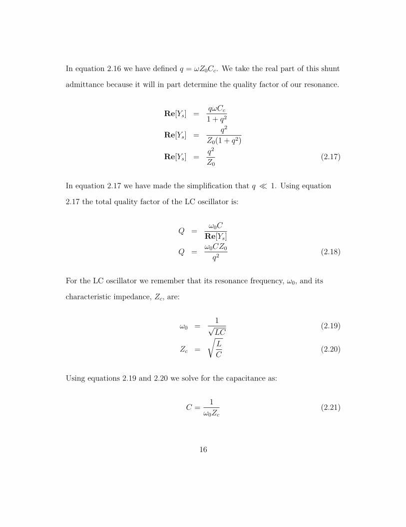
In equation 2.16 we have defined q = ωZ0Cc. We take the real part of this shunt
admittance because it will in part determine the quality factor of our resonance.
Re[Ys] =qωCc
1 + q2
Re[Ys] =q2
Z0(1 + q2)
Re[Ys] =q2
Z0
(2.17)
In equation 2.17 we have made the simplification that q ≪ 1. Using equation
2.17 the total quality factor of the LC oscillator is:
Q =ω0C
Re[Ys]
Q =ω0CZ0
q2(2.18)
For the LC oscillator we remember that its resonance frequency, ω0, and its
characteristic impedance, Zc, are:
ω0 =1√LC
(2.19)
Zc =
√L
C(2.20)
Using equations 2.19 and 2.20 we solve for the capacitance as:
C =1
ω0Zc
(2.21)
16

Now we simplify equation 2.18 by using equation 2.21:
Q =ω0CZ0
q2
Q =ω0(
1ω0Zc
)Z0
q2
Q =1
q2Z0
Zc
(2.22)
Q ≈ 1
q2(2.23)
q =1√Q
ω0Z0Cc =1√Q
Cc =1
ω0Z0
√Q
(2.24)
To go from 2.22 to equation 2.23 we make the approximation that the char-
acteristic impedance of the transmission line normalized by the characteristic
impedance of the LC oscillator is of order unity. From equation 2.24 we can
now estimate the strength of the capacitor needed to have a total quality fac-
tor of no worse than a million. If we assume a resonance at 8 GHz and a char-
acteristic impedance of 50 Ω then our coupling capacitor is 400 aF. For a total
quality factor of 1010 this would require a net coupling capacitor of 4 aF which
is incredibly small! This is why the evanescent coupling, which allows exponen-
tial suppression to the external environment, that we will explain in the next
chapter is so essential.
17

! = ! r + i! i Cr Gshunt
Ad
Figure 2.4: Lossy Parallel Plate Capacitor. To frame the discussion of participa-tion ratios a lossy parallel plate capacitor will be considered. The results fordescribing the lossy parallel plate capacitor will be quite general and not specificto this geometry. We decompose the lossy capacitor into an idealized capacitor,Cr shunted by a lossy element Gshunt.
2.5 Participation Ratios
In this final section, quality factors are used to develop the concept of participa-
tion ratios giving an implementation independent means to describe dissipation
in a RF circuit.
2.5.1 Lossy Capacitor
We begin our investigation into participation ratios by looking at a capacitor
whose loss originates from having a material with a complex dielectric constant,
ϵ = ϵr + iϵi (i =√−1). As a simple example we will look at a parallel plate
capacitor (Fig. 2.4) which we acknowledge for all frequencies is not a capacitor
[49] but nevertheless gives insight into the problem of handling a lossy capaci-
tor. In general, the admittance for a capacitor is simply:
Yc = jωC (2.25)
18

Where C is the capacitance of the object, ω is the angular frequency, and j is
in the standard electrical engineer definition (j = −i). In the case of a paral-
lel plate capacitor filled with a material with a complex dielectric constant the
capacitance for this parallel plate is:
Cpp = ϵA
d(2.26)
Where ϵ is the complex permittivity, A is the area of the plates, and d is the
distance for the plates (Fig. 2.4). If we use equation 2.26 in equation 2.25 then
the admittance for this lossy capacitor is:
Ycpp = jωϵA
d(2.27)
Explicitly writing out the complex permittivity equation 2.27 becomes:
Ycpp = jω(ϵr + iϵi)A
d
Ycpp = jωϵrA
d+ jiωϵi
A
d
Ycpp = jωϵrA
d+ ωϵi
A
d(2.28)
Ycpp = jωCr +Gshunt (2.29)
We rewrite our result in equation 2.28 as two terms in equation 2.29. The first
term in equation 2.29 stores energy in the E or D fields and acts as an idealized
capacitor. The second term in equation 2.29 is a dissipative term which shunts
the idealized capacitor. This shunt resistance, Gshunt, is not ohmic and has zero
19
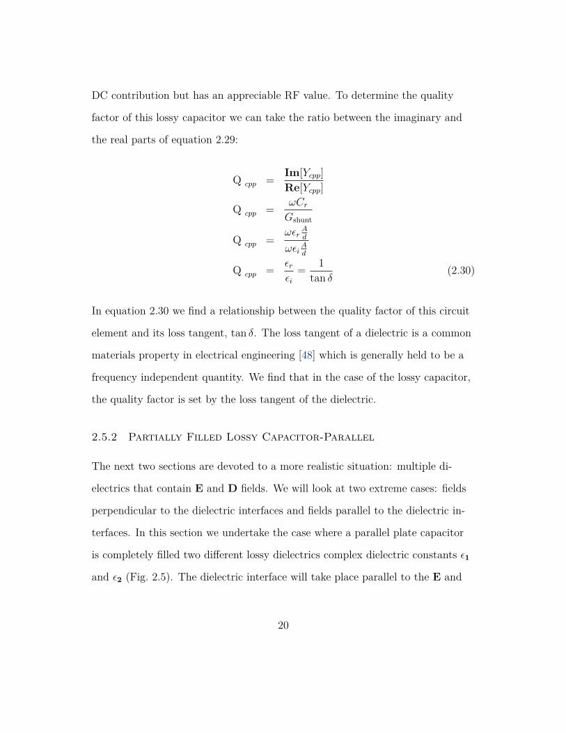
DC contribution but has an appreciable RF value. To determine the quality
factor of this lossy capacitor we can take the ratio between the imaginary and
the real parts of equation 2.29:
Q cpp =Im[Ycpp]
Re[Ycpp]
Q cpp =ωCr
Gshunt
Q cpp =ωϵr
Ad
ωϵiAd
Q cpp =ϵrϵi
=1
tan δ(2.30)
In equation 2.30 we find a relationship between the quality factor of this circuit
element and its loss tangent, tan δ. The loss tangent of a dielectric is a common
materials property in electrical engineering [48] which is generally held to be a
frequency independent quantity. We find that in the case of the lossy capacitor,
the quality factor is set by the loss tangent of the dielectric.
2.5.2 Partially Filled Lossy Capacitor-Parallel
The next two sections are devoted to a more realistic situation: multiple di-
electrics that contain E and D fields. We will look at two extreme cases: fields
perpendicular to the dielectric interfaces and fields parallel to the dielectric in-
terfaces. In this section we undertake the case where a parallel plate capacitor
is completely filled two different lossy dielectrics complex dielectric constants ϵ1
and ϵ2 (Fig. 2.5). The dielectric interface will take place parallel to the E and
20

d!1 = !1r + i!1i
!2 = !2r + i!2i
A1 A2C1 C2G1 G2
Figure 2.5: Lossy Capacitor-Two Dielectrics: Parallel. Parallel plate capacitorwith lossy dielectrics whose surface interface is parallel to E or D fields is con-sidered. The above case of a parallel plate capacitor filled with two differentcomplex dielectrics ϵ1,2 is presented. The two different regions can be modeledas an idealized capacitor C1,2 shunted by G1,2 with each region circuit equiva-lent being in parallel with the other regions circuit equivalent.
D fields. Since each section of dielectric has the same voltage across it, these
two lossy capacitors are in parallel. Following a similar formalism as in section
2.5.1 we can describe each region as a capacitor shunted by a resistor. If we as-
sume that for each dielectric there is a corresponding area, A1 , A2 then for the
capacitors in region 1 and 2 we have:
C1 = ϵ1rA1
d(2.31)
G1 = tan δ1C1ω (2.32)
C2 = ϵ2rA2
d(2.33)
G2 = tan δ2C2ω (2.34)
These circuit elements are all in parallel and it is straight forward to calculate
21
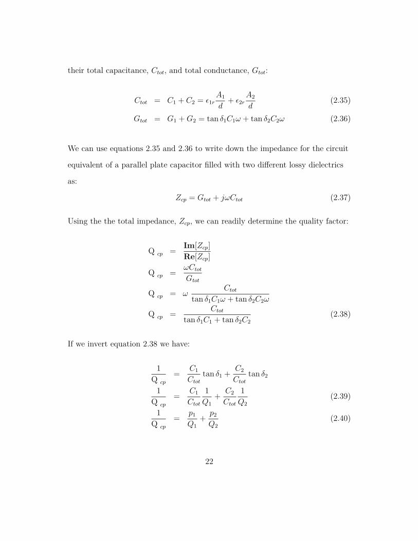
their total capacitance, Ctot, and total conductance, Gtot:
Ctot = C1 + C2 = ϵ1rA1
d+ ϵ2r
A2
d(2.35)
Gtot = G1 +G2 = tan δ1C1ω + tan δ2C2ω (2.36)
We can use equations 2.35 and 2.36 to write down the impedance for the circuit
equivalent of a parallel plate capacitor filled with two different lossy dielectrics
as:
Zcp = Gtot + jωCtot (2.37)
Using the the total impedance, Zcp, we can readily determine the quality factor:
Q cp =Im[Zcp]
Re[Zcp]
Q cp =ωCtot
Gtot
Q cp = ωCtot
tan δ1C1ω + tan δ2C2ω
Q cp =Ctot
tan δ1C1 + tan δ2C2
(2.38)
If we invert equation 2.38 we have:
1
Q cp
=C1
Ctot
tan δ1 +C2
Ctot
tan δ2
1
Q cp
=C1
Ctot
1
Q1
+C2
Ctot
1
Q2
(2.39)
1
Q cp
=p1Q1
+p2Q2
(2.40)
22
Equations 2.39 and 2.40 define the capacitive participation ratio in the case
where the field lines are parallel to the interface–explicitly pi =Ci
Ctot. Conceptu-
ally we understand this participation ratio to be the electric field energy stored
in the given region normalized by the entire electric field energy. The sum of
all participation ratios multiplied by their respective loss rate results in the to-
tal loss rate of the resonance and is inverse to the total quality factor. We gain
the intuition that if we must include lossy components then our circuit design
should be such that the lossiest part has the smallest participation ratio, mini-
mally spoiling the total quality factor.
For example, 3D resonators coupled to qubits with lifetimes of order 1 ms in
the 5-10 GHz [50, 51, 52] regime give total quality factors in excess of 107. If
we have a dielectric with a loss tangent of 10−5 in the quantum regime, then
no more than 1% of the total electric field energy can be stored in the lossy
dielectric. Furthermore, we can also consider manipulations on the quantum
state of a cavity that require conditional qubit rotations which take of order
1 µs [53, 54]. For qubit decay to be less than a percent during the cavity manip-
ulation, qubit lifetimes must also be of order 100 µs leading to the conclusion
that no more than 10% of the total electric field energy can be stored in a rel-
atively low loss dielectric. The major point is that the physicist must carefully
design the resonant circuit or artificial atom with participation ratios in mind so
to minimally spoil the coherence of the quantum system.
23

!1 = !1r + i!1i
!2 = !2r + i!2i
C1
C2
G1
G2
A
d1
d2
Figure 2.6: Lossy Capacitor-Partially Filled Series. To gain insight for how lossydielectrics which are parallel to E or D fields contribute to the total quality fac-tor, the above case of a parallel plate capacitor filled with two different complexdielectrics ϵ1,2 is presented. The two different regions can be modeled as an ide-alized capacitor C1,2 shunted by G1,2 with each region circuit equivalent being inseries with the other regions circuit equivalent.
24

2.5.3 Partially Filled Lossy Capacitor-Series
The other key case for a lossy capacitor is when it is filled with two different di-
electrics ϵ1 and ϵ2 whose interfaces are perpendicular to the E and D field lines
(Fig. 2.6). This partially filled capacitor can be modeled as two lossy capacitors
in series. Each lossy capacitor’s admittance is:
Ycs1 = jωC1 + ωC1 tan δ1 = G1 + jωC1 (2.41)
Ycs2 = jωC2 + ωC2 tan δ2 = G2 + jωC2 (2.42)
Where C1,2 = ϵ1,2rA
d1,2. We now combine these two series lossy capacitors to
determine the total impedance, Ztot:
Ztot =1
Ycs1
+1
Ycs2
Ztot =Ycs1 + Ycs2
Ycs1Ycs2
Ztot =jωC1 + ωC1 tan δ1 + jωC2 + ωC2 tan δ2(jωC1 + ωC1 tan δ1)(jωC2 + ωC2 tan δ2)
Ztot =jC1 + C1 tan δ1 + jC2 + C2 tan δ2
(jC1 + C1 tan δ1)(jωC2 + ωC2 tan δ2)
Ztot =jC1 + C1 tan δ1 + jC2 + C2 tan δ2
(jωC1C2 tan δ1 + ωC1C2 tan δ1 tan δ2 − ωC1C2 + jωC1C2 tan δ2)
Ztot =jC1 + C1 tan δ1 + jC2 + C2 tan δ2
(−ωC1C2(1− tan δ1 tan δ2) + jωC1C2(tan δ1 + tan δ2))
Ztot ≈ C2 tan δ1 + C1 tan δ2 + j(C1 + C2)
ωC1C2
(2.43)
25

We define Ctot =C1C2
C1+C2so that we can now determine the total quality factor:
1
Q tots
=Re[Ztot]
Im[Ztot]
1
Q tots
=
(tan δ1ωC1
+tan δ2ωC2
)(ωCtot)
1
Q tots
= p1 tan δ1 + p2 tan δ2 (2.44)
We arrive at similar result again. The total quality factor will be set by the
loss tangent of each item scaled by its participation ratio which in the case for
field lines perpendicular to the interface is pi = Ctot
Ci. If we use the parallel plate
capacitor as an example and look at one of the participation ratios we have:
p1 =Ctot
C1
=C2
C1 + C2
=ϵ2rA/d2
ϵ1rA/d1 + ϵ2rA/d2=
(1 +
ϵ1rϵ2r
d2d1
)−1
(2.45)
As one would expect the participation ratio for a given layer increases with
increasing relative thickness of the layer under investigation. A counter intu-
itive result is that by increasing the dielectric constant of a given layer actually
reduces the participation ratio! In planar resonators a method that has been
shown to increase the quality factor of the resonator is removing the dielectric
near the edges, trenching [55, 56, 57]. A possible method to improve on trench-
ing would be to use a material with a very large dielectric constant that can be
thinly deposited underneath the resonator. This could allow for more aggres-
sive trenching and structural support resulting in more energy stored in lossless
vacuum. The idea of trenching could also prove useful for superconducting ar-
26

A
l
µ = µr + iµi
L'
R
Figure 2.7: Lossy Inductor. To understand how lossy permeable material affectthe quality factor of an inductor we will analyze the case of a solenoid of lengthl, cross sectional area A, complex permeability µ, and whose number of termsper unit length is n. This lossy solenoid will be described as an idealized induc-tor L′ in series with a resistor R.
tificial atoms in the GHz frequency range, which unequivocally must be fabri-
cated through lithographic processes and metal deposition in contrast to cavities
which can be machined out of high purity superconductors.
2.5.4 Lossy Inductor
Up until this point all the discussion of participation ratios has been in terms of
the E and D fields. However, we can and will produce analogous results for B
and H fields. In a similar fashion to the lossy parallel plate capacitor we begin
with a solenoid filled with a lossy material. The solenoid consists of n turns per
unit length, is filled with a lossy material with a complex permeability µ, has an
cross sectional area A, and length l. The inductance for the lossy solenoid is:
L = µn2Al (2.46)
27
Using equation 2.46 the impedance of a lossy solenoid is:
Zsolenoid = jωL = jωµn2Al = jω(µr+iµi)n2Al = ωµin
2Al+jωµrn2Al = R+jωL′
(2.47)
From the solenoid impedance the quality factor can be calculated as:
Q solenoid =Im[Zsolenoid]
Re[Zsolenoid]
Q solenoid =µrωn
2Al
µiωn2Al
Q solenoid =µr
µi
(2.48)
Q solenoid =1
tan δl(2.49)
Where in equation 2.49 we have defined an analogous loss tangent for perme-
able materials as tan δl =µi
µr. In the same manner as with the lossy capacitor, in
the case of the lossy inductor its quality factor will be set by its inductive loss
tangent.
2.5.5 Partially Filled Lossy Inductor-Series
Now we begin our treatment of inductors that have two different lossy per-
meable cores. In this section, we undertake the situation where the B and H
fields are perpendicular to the surface interface of the two permeable materials
(Fig. 2.8). The inductance for either region is:
L1,2 = µr 1,2n2Al1,2 (2.50)
28

A L1R1L2R2
l1
l2
µ1 = µ1r + iµ1i
µ2 = µ2r + iµ2i
Figure 2.8: Lossy Inductor-Partially Filled Series. In the above, a solenoid is filledwith two different permeable materials with complex permeabilities µ1,2 whoseinterface is perpendicular to the B and H fields in the solenoid. By rewrit-ing this as idealized inductors L1,2 and resistors R1,2 we gain insight as to howthese permeable materials affect the total quality factor. It is also worth notingthat the resistance we discuss here is non-ohmic and has zero DC resistance butnonzero resistance at RF frequencies.
We can also use equation 2.50 to readily write down the resistance in either re-
gion as:
R1,2 = ω tan δl 1,2L1,2 (2.51)
Using equations 2.50, 2.51, and that these idealized circuit elements are in series
the total inductance and resistance are:
Ltot = n2A(µr 1l1 + µr 2l2) (2.52)
Rtot = ωn2A(tan δl 1µr 1l1 + tan δl 2µr 2l2) (2.53)
29

From equations 2.52 and 2.53 the quality factor of the lossy solenoid is:
1
Q tots
=Re[Ztot]
Im[Ztot]
1
Q tots
=Rtot
ωLtot
1
Q tots
=ωn2A(tan δl 1µr 1l1 + tan δl 2µr 2l2)
ωn2A(µr 1l1 + µr 2l2)
1
Q tots
=tan δl 1µr 1l1 + tan δl 2µr 2l2
µr 1l1 + µr 2l2(2.54)
1
Q tots
= p1 tan δl 1 + p2 tan δl 2 (2.55)
Where we have defined the participation ratios for the B and H fields when the
permeable materials are in series as pi = µr ili/(Σµr jlj). As expected the sec-
tions with longest length and highest permeability contribute most to the total
quality factor.
2.5.6 Partially Filled Lossy Inductor-Parallel
In this final section, we under take the case that a solenoid is entirely filled with
permeable material but that the interface between two distinct regions is per-
pendicular to the B and H fields (Fig. 2.9). Each section will have an induc-
tance and resistance of:
L1,2 = µr 1,2n2A1,2l (2.56)
R1,2 = ω tan δ1,2L1,2 (2.57)
30

L1R1
L2R2
µ1 = µ1r + iµ1i
µ2 = µ2r + iµ2i
l
A1
A2
Figure 2.9: Lossy Inductor-Partially Filled Series. In the above, a solenoid is filledwith two different permeable materials with complex permeabilities µ1,2 whoseinterface is parallel to the B and H fields in the solenoid. By rewriting this asidealized inductors L1,2 and resistors R1,2 we gain insight as to how these per-meable materials affect the total quality factor.
The impedance for either region can be written as:
Z1,2 = R1,2 + jωL1,2 (2.58)
Since these two regions are in parallel we combine them to find their total impedance:
Znet =Z1Z2
Z1 + Z2
Znet =(R1 + jωL1)(R2 + jωL2)
R1 +R2 + jω(L1 + L2)
Znet =(R1 + jωL1)(R2 + jωL2)(R1 +R2 − jω(L1 + L2))
(R1 +R2)2 + ω2(L1 + L2)2
Znet ≈ ω2L21R2 + ω2L2
2R1 + jω3L1L2(L1 + L2)
ω2(L1 + L2)2(2.59)
31

Now to determine the quality factor of this solenoid we again take the ratio of
the imaginary part of the net impedance to the real part:
1
Q totp
=Re[Ztot]
Im[Ztot]
1
Q totp
=ω2L2
1R2 + ω2L22R1
ω3L1L2(L1 + L2)
1
Q totp
=L2
1R2 + L22R1
ωL1L2(L1 + L2)
1
Q totp
=L21ω tan δl 2L2 + L2
2ω tan δl 1L1
ωL1L2(L1 + L2)
1
Q totp
=L1 tan δl 2 + L2 tan δl 1
L1 + L2
1
Q totp
=Ltot
L2
tan δl 2 +Ltot
L1
tan δl 1 (2.60)
1
Q totp
= p2 tan δl 2 + p1 tan δl 1 (2.61)
Where we have used that the total inductance is Ltot = L1L2
L1+L2. We use the
total inductance to define the participation ratio for each element as pi = Ltot
Li.
In the case of a solenoid we can find the participation ratio to be:
p1 =Ltot
L1
p1 =L2
L1 + L2
p1 =µr 2n
2A2l
µr 1n2A1l + µr 2n2A2l
p1 =
(µr 1
µr 2
A1
A2
+ 1
)−1
(2.62)
32

From this we find two surprising results. That the participation ratio increases
for smaller areas and for smaller permeabilities! Once again we find a scenario
where a small bit of vacuum could substantially improve the quality factor of a
resonator. It is not too surprising that this case would be the one with a bene-
ficial outcome since an electromagnetic wave in free space has the electric and
magnetic fields perpendicular to each other. From the results of section 2.5.3
for the electric field participation ratios we could have naively guessed that the
orthogonal magnetic field would scale similarly; however, it is quite nice that it
did work out to be the case.
2.6 Final Thoughts
The major ideas we have developed in this chapter, quality factors and partic-
ipation ratios, will be used extensively in the next two chapters which are on
the physical implementation of microwave cavities and resonators. Quality fac-
tors give a frequency independent way to quantify the loss of a resonant mode.
Although two cavities or qubits could have the same quality factor for their res-
onance those with lower frequencies have longer lifetimes from equation 2.13.
Also, participation ratios give a means to quantify resonances with similar qual-
ity factors by being able to break down the contributing loss mechanisms to see
if results are consistent or inconsistent.
33

3Transmission Line Resonators
The main goal of this chapter is to describe and adapt a microwave geometry
for circuit quantum electrodynamics. Cavities with lifetimes in excess of 1 ms in
the quantum regime [58, 50, 51, 52] can be constructed from bulk superconduc-
tors materials. However, to access the rich physics of cQED it is necessary to
have an atomic like object [59]. In cQED the atomic like object relies originates
34

from the Josephson junction. Incorporating a Josephson junction to realize res-
onances in the 5-10 GHz range requires fabrication with lithography and deposi-
tion making fabrication nano-fabrication an essential part of cQED. Thoughtful
integration is required to build more complex structures while maintaing the
coherence found in waveguide cavities. To fulfill this demand, we seek to imple-
ment a novel, lithographically defined transmission line geometry. As we will
see, the transmission line structure can realize a resonant cavity. This resonant
cavity in principle can be used for: state readout of the ‘artificial atom’, pro-
tecting the ‘artificial atom’ from radiating into the environment, and serving as
a test bed for different superconducting materials, dielectrics, and lithographic
procedures.
3.1 Historical Development
Microwave circuits are by no means a new development as their use date back
to the 1930s. Although waveguide structures were quite successful in the 1940s,
the desire for an increased bandwidth as well as complexity and integration
spurred the development of two new geometries: stripline and microstrip [60]
(Fig. 3.1). The invention of the stripline architecture is credited to Robert M.
Barrett in the 1950s at the Air Force Cambridge Research Center [60]. The
original development by Barrett used dielectric materials only to support the
center conductor between the two ground planes (Fig. 3.1 C). Although now
any structure with a flat conductor between two ground planes is referred to as
a stripline, in the 1950s if the device was mostly filled by vacuum then it was
35

called a stripline and if the device was filled entirely with a dielectric material it
was referred to as “tri-plate” (Fig. 3.1 B). Striplines were an attractive geome-
try for microwave engineers in part because it is a TEM structure with no cut
off frequency. At the same time the stripline was being developed so too was
the microstrip geometry (Fig. 3.1 A). The microstrip relies on the fields being
concentrated between the center conductor and a sole ground plane. Issues with
the microstrip geometry are radiative losses as well as a greatly distorted phase
velocity due to the large difference in dielectrics. For improved performance mi-
crostrips typically need an enclosure and for this reason we elect to develop a
stripline structure.
3.2 Characteristic Impedance
Figure 3.2 shows the prototypical stripline. The ground planes are separated
by a distance, H, filled with a dielectric with relative dielectric ϵr, and with the
center conductor placed symmetrically between the ground planes. The center
conductor has a width, W , and thickness, t. Since there are two conductors this
is a TEM structure [48]. Closed form solutions to the characteristic impedance,
Zc, of this transmission line exist [61]; however, a more simplified form that does
not deviate by more than 1% [48] of the true value is:
Zc =60√ϵr
ln
(4H
.67πW (.8 + tW)
)(3.1)
In our particular case the thickness will be 200 nm or less and the widths will
36

A B C
Figure 3.1: In all sketches, a conducting strip (blue) is deposited on a substrate(yellow) and then kept a distance away from another conductor, ground, (grey).In all cases, electric field lines are drawn in red and magnetic field lines aredrawn as green dashed lines. A a cartoon figure of a microstrip geometry whichhas only one ground plane and is quasi-TEM transmission line [48]. B A car-toon schematic of a tri-plate structure which is a center conductor fully sur-rounded by a dielectric substrate with a top and bottom ground plane. C Acartoon schematic of the original stripline design where the center conductor isdeposited on a substrate only thick enough to provide mechanical support andis mostly vacuum (air). As we saw in chapter 2, the electric field energy den-sity will be greater in the region with the lower dielectric constant if the electricfield is perpendicular at the interface so in the original stripline design the ma-jority of the electric field energy will reside in vacuum (air). The substrate sitsbetween two conducting ground planes and is a TEM transmission line [48]. Allsketches of microstrip, tri-plate, and striplines with electric and magnetic fieldsbased on Ref. [60].
37

! r
tW H
2
H2
Figure 3.2: Prototypical stripline. The ground planes (grey) are separated by adistance, H, filled with a dielectric with relative dielectric ϵr (yellow), and withthe center conductor (blue) placed symmetrically between the ground planes.The center conductor has a width, W , and thickness, t.
be 300 microns or more so we can neglect the tW
contribution and simplify eq.
3.1 to:
Zc =60√ϵr
ln
(4H
.54πW
)(3.2)
We can use the above to gain some intuition as to the relative sizes our phys-
ical structure requires. For this structure to have a characteristic impedance of
50 Ω, assuming ϵr = 10, the height to width ratio is roughly a factor of 5. In
this thesis, a height to width ratio of 3 was used. The smaller height to width
ratio is a consequence of the dielectric being roughly half vacuum.
3.3 Design Consideration
In this section, we undertake the design of a stripline structure that will be
readily compatible with the standard cQED environment. We seek to minimize
fabrication steps required and elect to construct the grounding structure out of
38
bulk superconductor so different chips can be readily swapped in and out. The
thought process was to minimize the ambiguity in future results that depend on
complicated fabrication and deposition procedures. A substrate inserted into the
superconducting structure will have a deposited thin film which acts as the cen-
ter pin for the stripline structure. By having a finite length of the center con-
ductor we can realize a half wave length resonator with respect to the voltage
on the center pin.
Since we will be building an enclosed stripline to minimize radiative and en-
vironmental losses we must acknowledge that the enclosure is really a rectangu-
lar waveguide. We will design this rectangular waveguide to have a high cutoff
frequency (> 20 GHz) to avoid any extraneous modes coupling to our supercon-
ducting structures. The cutoff frequency, fc,mn, of the rectangular waveguide,
with sides of length a and b, is [48]:
fc,mn =c
2π√µrϵr
√(mπ
a
)2
+(nπ
b
)2
(3.3)
In equation 3.3, c is the speed of light in vacuum, µr and ϵr are the relative per-
meability and permitivity respectfully, and m,n are the different transverse
mode indices. Rectangular waveguides are analyzed as a single conductor and
consequently cannot support TEM wave propagation. For this reason, the rect-
angular waveguide can only support TEmn or TMmn modes. Equation 3.3 gives
the cut off frequency for either TEmn or TMmn modes. In our design we care
only about the frequency that the first mode of the structure that propagates
rather than higher modes. The lowest mode will be the TE10 defined by the
39

a
b
c
Figure 3.3: Rectangular Waveguide Cavity. A rectangular waveguide with di-mensions a (red), b (blue), and c (green). Shown in blue and green arrows arethe amplitude of the electric field along either the b, c directions which due toboundary conditions must be zero at the walls of the rectangular waveguide cav-ity.
longest side of the rectangle [48]:
fc,10 =c
2a√µrϵr
(3.4)
The longest length that can be tolerated for a cutoff frequency of 20 GHz is
roughly 5mm assuming that the waveguide is fully filled with a relative dielec-
tric of 10. Decreasing the relative dielectric will increase the cutoff frequency
and consequently increase the relevant length scale.
A similar consideration to investigate is the consequence of having a finite
length rectangular waveguide. The sample box itself is rectangular (figure 3.3),
40

with sides a, b, and c, and will have resonance frequencies given by [48]:
fmnl =c
2π√µrϵr
√(mπ
a
)2
+(nπ
b
)2
+
(lπ
c
)2
(3.5)
In equation 3.5 c is the speed of light in vacuum, µr and ϵr are the relative per-
meability and permitivity respectfully, and m,n are the different transverse
mode indices and l is the longitudinal index. Once again the dominant mode,
lowest frequency, will be the TE101. This assumes that c > a > b which means
that the external conductor will be longer than either of the sides making up
the cross-sectional rectangle. From equation 3.5 we gain the insight that the
longer we make the structure the less it depends on the length. For a TE101
mode, in the limit that c ≫ a equation 3.5 reduces to equation 3.4 but has the
interpretation of being a resonance frequency rather than the cutoff frequency.
3.4 First Design
In the first design we choose the width of our rectangular cross section to be
1.2 mm, the height to be 1mm, and the length of the structure to be 25mm. If
the structure were entirely filled with ϵr = 10 then the cutoff frequency from
equation 3.4 is 40 GHz. If the relative dielectric is smaller than that only in-
creases the cutoff frequency. The resonant mode of this holder will also be ap-
proximately 40 GHz because of the extreme length to width ratio.
Figure 3.10a, b contain diagrams with cross sections of the enclosed stripline
that will be the focus of this chapter. We have chosen to have a very narrow
41

1.2mm
1mm
a 25mm
1mm
b
c
25mm
Sapphire
Al/Nb
Vacuum
Al
Sapphire
Al/Nb
Al
Al/Nb Al/Nb
λ/2
Al
Al
Sapphire
SMASMA
Wire bonds
Wire bonds
Figure 3.4: First generation stripline design. a) Cross section of design. In grey is the outerconductor whose internal dimensions are 1 mm by 1.2 mm. In yellow is the substrate for thedeposited film (blue). The substrate primarily used is sapphire; however, any dielectric can beused. This structure is flexible enough to accommodate many different dielectrics and conduc-tors to measure their loss. b) Side cut lengthwise down holder. In grey is the outer conductorwhose total length is 25 mm and height is 1mm. In yellow is the dielectric material with de-posited superconducting material (blue and green). Although different colors are used thesuperconducting material is the same. In green are the superconducting leads which are gapcoupled to the superconducting half wave length resonator, blue. c) Photo of actual sample.The external structure has two symmetric halves that close into each other. One half has thesapphire substrate with the deposited superconductor. SMA connectors are wire-bonded tothe superconducting leads to allow measurement of the resonator.
42

structure to force all undesired modes to be quite high in frequency. All though
most of the discussion up until this point has discussed the stripline with a uni-
formly filled dielectric we have elected to only partially fill the structure. The
main reason for this decision is for frequency stability. In preliminary tests it
was found that adding in dielectric on top would cause fluctuations in the fre-
quency of the resonator. As we will see later even with half filled dielectric it
accounts for roughly 90% of the electric participation ratio so adding dielectric
on top was an unnecessary complication in the early development.
3.5 Participation Ratios
In this section we undertake analytically calculating participation ratios for
both the surface loss of a lossy dielectric and the bulk loss of a dielectric in a
stripline geometry. To achieve these calculations one must make some approxi-
mations that are not exact in real experiments. The goal with these analytical
calculations is not to accurately calculate participation ratios to arbitrary preci-
sion but rather to give the experimentalist intuition for the order of magnitude
of loss and what to expect when a given geometry is changed.
To accurately calculate a participation ratio is is essential for one to use a fi-
nite elemental solver. The software of choice in this thesis is Ansys’ HFSS (High
Frequency Structural Simulator). HFSS allows one to draw all structures in a
CAD environment and solve for the scattering, impedance, or admittance ma-
trices. HFSS partitions the drawn structure into many small tetrahedrals and
solves Maxwell’s equations inside each tetrahedral. Since HFSS solves for the
43
electric and magnetic fields it is relatively straight forward to use their fields
calculator to sum the electric or magnetic field energy in a given region or vol-
ume. One can setup the field calculation ahead of time to calculate a participa-
tion ratio and then use the participation ratio as the numerical quantity that is
used to determine whether or not a solution converged. Additionally, HFSS can
be used to simulate Hamiltonian parameters which is discussed in chapter 4.
3.5.1 Surface Dielectric Loss
We now undertake calculating dielectric losses to know how loss will determine
our quality factors as well as give insight into which knobs we have available
to change as an experimental parameter. First we will calculate the loss from
dielectric surfaces. The total energy per unit length stored in the electric field of
a stripline of length L, with capacitance per unit length, c, and voltage, V , is:
Utot
L=
1
2cV 2 (3.6)
To calculate the energy per unit length stored in the lossy dielectric of thick-
ness t and length L we must calculate the following integral:
Usurf =1
2Lt
∫ϵ|Esurf |2dw
(3.7)
To evaluate equation 3.7 we must determine Esurf . Assuming a uniform charge
44

per unit area, σ, on the center conductor the electric field is:
Esurf =σ
ϵ0ϵr(3.8)
We can rewrite Esurf in terms of the total charge, Q, and the length, L, and
width, W , of the center conductor equation 3.8 becomes:
Esurf =σ
ϵ0ϵr=
Q
LWϵ0ϵr(3.9)
We can rewrite equation 3.9 by using the capacitance relation between the charge
per unit length, the capacitance per unit length, and the voltage:
Q
L= cV (3.10)
With equations 3.9 and 3.10 we can find the surface electric field is:
Esurf =cV
Wϵ0ϵr(3.11)
Using equation 3.11 in equation 3.7 we can determine the energy per unit length
stored in the lossy surface dielectric:
Usurf =1
2Lt
∫ϵ|Esurf |2dW
Usurf =1
2LtWϵ0ϵr
(cV
Wϵ0ϵr
)2
Usurf
L=
1
2
t
Wϵ0ϵr(cV )2
45

We can now calculate the participation ratio for a lossy surface dielectric for the
stripline using equations 3.6 and 3.10 is:
psurf =
(Usurf
L
)(Utot
L
)−1
psurf =
(1
2
t
Wϵ0ϵr(cV )2
)(1
2cV 2
)−1
psurf =tc
Wϵ0ϵr
We find that the surface participation ratio is dependent mostly on well defined
quantities such as the thickness of the lossy dielectric, t, its width, w, and the
relative dielectric constant, ϵr. The only unknown quantity we need to deter-
mine is the capacitance per unit length, c. We remember that for a transmission
line its characteristic impedance in terms of its inductance per unit length l and
capacitance per unit length c is:
Zc =
√l
c(3.12)
Also, the speed of light in the transmission line is:
v =1√lc
(3.13)
Using equations 3.12 and 3.13 we can solve for the capacitance per unit length
as:
c =1
Zcv(3.14)
46

Now we can rewrite the surface participation ratio using equation 3.14 as:
psurf =t
Wϵ0ϵrZcv(3.15)
We can further simplify this by using that velocity of light in the transmission
line in terms of the speed of light c and the relative dielectric constant ϵr is
v =c
√ϵr:
psurf =t
Wϵ0√ϵrZcc
(3.16)
Plotted in figure 3.5 is equation 3.16 as a function of center trace width for real-
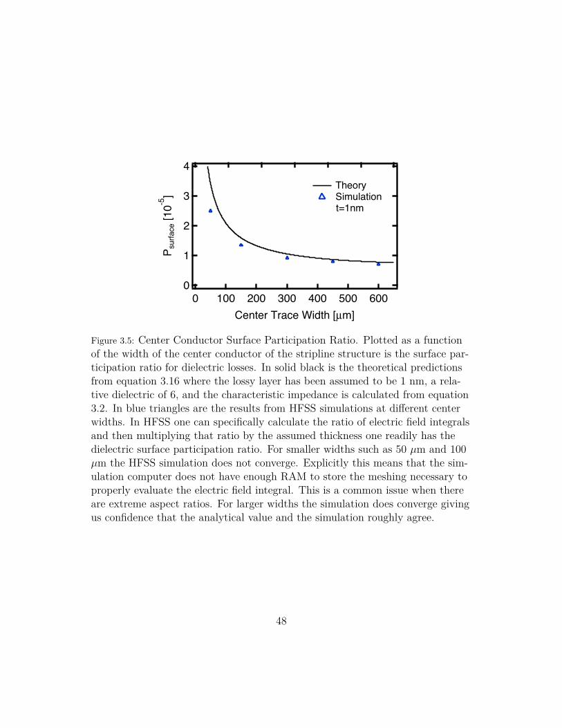
istic parameters. As an example, we can use equation 3.16 for a typical stripline
geometry. For a lossy surface layer with thickness of 3 nm, a center conductor
width of 300 µm, relative dielectric of 6, and Zc = 50 Ω from equation 3.2, we
get a surface participation ratio of order ∼ 10−5. From this we learn that to
have a total quality factor in excess of a million the lossy surface layer need only
have a quality factor of ten. However, at the writing of this thesis the state of
the art cavity lifetime when coupled to a qubit is of order 1 ms which if realized
in a stripline geometry requires the lossy layer to have a quality factor no worse
than a few hundred.
3.5.2 Bulk Dielectric Loss
The bulk dielectric loss will be a more straight forward calculation than the
surface dielectric loss. We assume that the center conductor is symmetrically
placed between the ground planes. To determine the energy stored in the dielec-
47
4
3
2
1
0
P sur
face
[10-5
]
6005004003002001000Center Trace Width [µm]
Theory Simulation
t=1nm
Figure 3.5: Center Conductor Surface Participation Ratio. Plotted as a functionof the width of the center conductor of the stripline structure is the surface par-ticipation ratio for dielectric losses. In solid black is the theoretical predictionsfrom equation 3.16 where the lossy layer has been assumed to be 1 nm, a rela-tive dielectric of 6, and the characteristic impedance is calculated from equation3.2. In blue triangles are the results from HFSS simulations at different centerwidths. In HFSS one can specifically calculate the ratio of electric field integralsand then multiplying that ratio by the assumed thickness one readily has thedielectric surface participation ratio. For smaller widths such as 50 µm and 100µm the HFSS simulation does not converge. Explicitly this means that the sim-ulation computer does not have enough RAM to store the meshing necessary toproperly evaluate the electric field integral. This is a common issue when thereare extreme aspect ratios. For larger widths the simulation does converge givingus confidence that the analytical value and the simulation roughly agree.
48

tric substrate we need only compare the energy stored in the dielectric to the
total energy stored. Therefore the electric field energy stored in the dielectric is:
Ubulk =1
2
∫ϵ0ϵr|E|2dV (3.17)
The energy stored in vacuum will be:
Uvac =1
2
∫ϵ0|E|2dV (3.18)
The bulk participation ratio pE is then:
pE =Ubulk
Uvac + Ubulk
pE =12
∫ϵ0ϵr|E|2dV
12
∫ϵ0|E|2dV + 1
2
∫ϵ0ϵr|E|2dV
pE =ϵr
1 + ϵr(3.19)
For sapphire we can take ϵr = 10 and then pE = .91 which agrees with an HFSS
simulation giving the bulk dielectric participation ratio as pE = .92.
3.5.3 Inductive losses and Kinetic Inductance Ratio
To calculate the kinetic inductance ratio, α, between the center pin and the to-
tal geometric inductance we begin with the reactance associated with the ki-
netic inductance of a superconductor with uniform current density:
Xk = ωµ0λ0 = ωLk (3.20)
49

In equation 3.20, ω is frequency, µ0 is the free space permeability, and λ0 is the
London penetration depth of the superconductor, and we have defined the prod-
uct µ0λ0 as the kinetic inductance, Lk. We now say that the superconducting
strip has a width, w, which we divide by to get the kinetic inductance per unit
length:
lk =Lk
w=
µ0λ0
w(3.21)
Now the kinetic inductance ratio can be formally defined in terms of the kinetic
inductance per unit length, lk, and the geometric inductance per unit length, lg,
as:
α =lklg
(3.22)
To determine lg we use the characteristic impedance of the transmission line its
propagation velocity v =1√
lgcg.
Z0 =
√lgcg
lg =Z0
√ϵr
c(3.23)
Using equations 3.21 and 3.23 in equation 3.22 yields:
αsl =lklg
=µ0λ0c
wZ0√ϵr
(3.24)
Equation 3.24 depends mostly on fundamental or materials properties and the
only external knob we have as an experimentalist is the width of the center
50

1.6
1.2
0.8
0.4
0.0
Kine
tic In
duct
ance
Rat
io [1
0-3]
600500400300200100Center Trace Width [µm]
Theory Simulation
λ0=50nm
Figure 3.6: Kinetic Inductance Calculation. Kinetic inductance ratio is plottedas a function of the center conductor width of the stripline. The solid line isequation 3.24 with λ0 = 50nm, ϵr = 6, and Z0 calculated from equation 3.2.In blue triangles are the results from HFSS simulations done where the mag-netic field integrals are specifically evaluated. This once again gives the benefitof only needing to scale the simulation result by the London penetration length.As in figure 3.5, for smaller widths the simulation is unable to converge on avalue. An additional discrepancy is that for equation 3.24 a uniform current dis-tribution is assumed whereas in simulation a non-uniform current distributionis observed. Regardless, both simulation and analytical values are still within afactor of two so our intuition and order of magnitude estimate are correct.
trace. Although the characteristic impedance will also change dependent on
the width of the center strip as in equation 3.2 the dependence is weak (log-
arithmic). Plotted in figure 3.6 is a plot of the kinetic inductance fraction for
realistic values of the stripline structure.
51
3.6 Evanescent Coupling
In this section we will describe the coupling between stripline structures under
the umbrella of evanescent coupling. The conceptual idea is that we will send
a wave at a barrier that does not allow propagation at the intended frequency;
however, on the other side of the barrier is another region where the wave can
propagate. It has long been known for electromagnetic waves that evanescent
coupling is possible and is well described by Feynman [49]. Evanescent coupling
has been successfully leveraged for measurements in the quantum regime with
3D cavities [58, 62, 63, 64]. In the case of the stripline we will have the scenario
where the incoming signal is propagating down the transmission line structure,
it will then encounter a rectangular cavity with a signal frequency below the
cutoff of the wave guide exponentially reflecting the signal based on the length
of the waveguide. Finally, the signal in the waveguide below cutoff is met with a
half wavelength resonator formed in the stripline. At each boundary the overlap
between the electric and magnetic fields of the different modes will determine
which modes participate and control the coupling. Although closed form solu-
tions do not exist for TEM wave propagating down the stripline, from the field
lines in 3.1 we can approximate the transverse electric and magnetic fields as
52

[65]:
Ex,TEM(x, y, z) = −E0x cos(πx
a
)sin
(πyb
)e j(βz−ωt) (3.25)
Ey,TEM(x, y, z) = −E0y sin(πx
a
)cos
(πyb
)e j(βz−ωt) (3.26)
Hx,TEM(x, y, z) = H0x sin(πx
a
)cos
(πyb
)e j(βz−ωt) (3.27)
Hy,TEM(x, y, z) = −H0y cos(πx
a
)sin
(πyb
)e j(βz−ωt) (3.28)
Since this is a TEM structure the propagation constant, β, is equal to the wave
number–explicitly, β = k =2π
λ. We must determine the overlap between this
mode and the possible modes of the rectangular waveguide which cannot sup-
port TEM waves but can support either transverse electric, TEmn, or transverse
magnetic, TMmn, modes. The TEmn modes are [48]:
Ex,TE(x, y, z) =jωµnπ
k2cb
Amn cos(mπx
a
)sin
(nπyb
)e j(βz−ωt) (3.29)
Ey,TE(x, y, z) = −jωµnπ
k2ca
Amn sin(mπx
a
)cos
(nπyb
)e j(βz−ωt) (3.30)
Hx,TE(x, y, z) =jβmπ
k2ca
Amn sin(mπx
a
)cos
(nπyb
)e j(βz−ωt) (3.31)
Hy,TE(x, y, z) =jβmπ
k2cb
Amn cos(mπx
a
)sin
(nπyb
)e j(βz−ωt) (3.32)
53

Likewise the TMmn modes of the rectangular waveguide are [48]:
Ex,TM(x, y, z) = −jβmπ
k2ca
Bmn cos(mπx
a
)sin
(nπyb
)e j(βz−ωt) (3.33)
Ey,TM(x, y, z) = −jβnπ
k2cb
Bmn sin(mπx
a
)cos
(nπyb
)e j(βz−ωt) (3.34)
Hx,TM(x, y, z) =jωϵmπ
k2cb
Bmn sin(mπx
a
)cos
(nπyb
)e j(βz−ωt) (3.35)
Hy,TM(x, y, z) = −jωϵmπ
k2ca
Bmn cos(mπx
a
)sin
(nπyb
)e j(βz−ωt) (3.36)
The propagation constant in the waveguide will be determined by the wave
number k and the cutoff wave number kc. Explicitly:
β =√
k2 − k2c (3.37)
If k < kc we get some neat physics. The propagation constant becomes imag-
inary and instead of a propagating wave an exponentially reflected wave is the
solution in the given region. From equation 3.37 we see that higher cutoff wave
numbers, higher frequencies, will reflect more of the signal. This means we are
concerned most with the first rectangular waveguide mode that has a nonzero
overlap with the incoming TEM wave because that will be the dominant trans-
fer of electromagnetic waves. By computing the overlap:
O =
∫ a
0
∫ b
0
ETEM · ETE/TMdxdy (3.38)
54
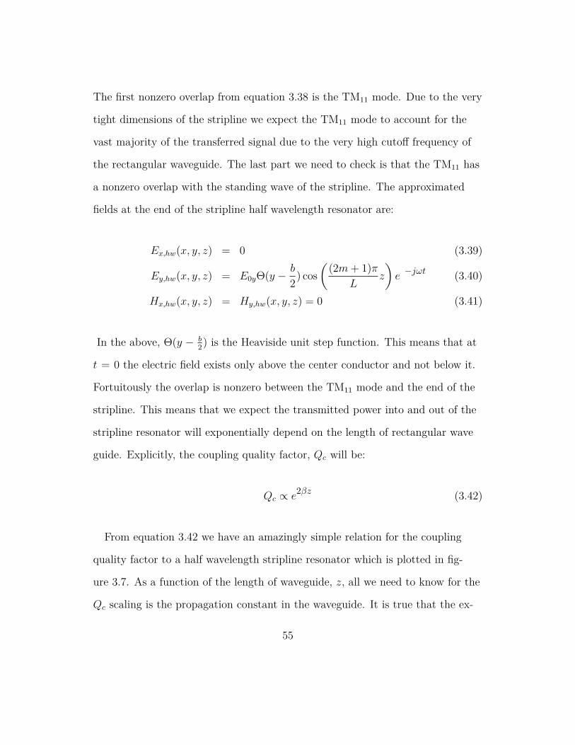
The first nonzero overlap from equation 3.38 is the TM11 mode. Due to the very
tight dimensions of the stripline we expect the TM11 mode to account for the
vast majority of the transferred signal due to the very high cutoff frequency of
the rectangular waveguide. The last part we need to check is that the TM11 has
a nonzero overlap with the standing wave of the stripline. The approximated
fields at the end of the stripline half wavelength resonator are:
Ex,hw(x, y, z) = 0 (3.39)
Ey,hw(x, y, z) = E0yΘ(y − b
2) cos
((2m+ 1)π
Lz
)e −jωt (3.40)
Hx,hw(x, y, z) = Hy,hw(x, y, z) = 0 (3.41)
In the above, Θ(y − b2) is the Heaviside unit step function. This means that at
t = 0 the electric field exists only above the center conductor and not below it.
Fortuitously the overlap is nonzero between the TM11 mode and the end of the
stripline. This means that we expect the transmitted power into and out of the
stripline resonator will exponentially depend on the length of rectangular wave
guide. Explicitly, the coupling quality factor, Qc will be:
Qc ∝ e2βz (3.42)
From equation 3.42 we have an amazingly simple relation for the coupling
quality factor to a half wavelength stripline resonator which is plotted in fig-
ure 3.7. As a function of the length of waveguide, z, all we need to know for the
Qc scaling is the propagation constant in the waveguide. It is true that the ex-
55

100
102
104
106
108Q
coup
le
806040200Distance [mils]
Room Temperature Data Simulation Evanescent Coupling TM11
a b
101
103
105
107
109
Qco
uple
16001200800400Gap [microns]
Evanescent coupling TM11 Evanescent coupling TE01 Simulation First generation stripline
Figure 3.7: Evanescent Coupling to 3D Cavity and Stripline. In both figures thecoupling quality factor is obtained through room temperature measurementsof |S21|2 using the formula derived in section 5.4.1. a) Evanescent coupling toa rectangular waveguide cavity. Plotted as a blue dashed line are results froman HFSS simulation where one varies the distance between a rectangular waveguide cavity and the distance to the coupler pin. As the pin is retracted ex-ponential growth of the coupling quality factor is observed. Plotted as a solidblack line is an analytical prediction for the rectangular waveguide cavity basedon the same principles used in section 3.6. The procedure used only gives thescaling (slope in the above plot). The first value of the analytical result is nor-malized to have the same value as the simulation and then plotted based on the‘2β’ value which is the slope. As points is data measured at room temperaturein incremental steps. Excellent agreement is found between all three. b) Evanes-cent coupling to a stripline resonator. The dashing blue line is the results forcoupling quality factor from an HFSS measurement as the distance between theresonator and incoming leads is increased. In solid black, is a line normalized tothe first coupling quality factor found from simulation and whose slope is deter-mined from the ‘2β’ value calculated for the stripline. In green, is a line predict-ing the coupling quality factor if the stripline was coupled to the lowest modeallowed to propagate in the rectangular waveguide which has a 2β = 5.2mm−1.In red are measurements performed at room temperature of the stripline setup.The slope of the measurements, 2β = 2.7mm−1, is substantially different thantheoretical, 2β = 8.2mm−1 and simulated predictions, 2β = 8.3mm−1. It seemsthat no matter how long the gap is between the resonator and the leads a resid-ual coupling remains. In green are measurements of coupling quality factor car-ried out in an indium coated stripline holder that is then welded together. Theslope from this data seems to be better in line with what is expected.
56

act propagation constant for a rectangular waveguide cavity partially filled with
dielectric requires solving a transcendental equation corresponding to the ex-
act mode in the waveguide [48]. However, due to the small cross section of the
rectangular waveguide (1mm by 1.2mm) the propagation constant is changed
by less than a .5% between vacuum or filled entirely with sapphire (ϵr = 10).
For these reasons we will use the relative dielectric constant of 6 and not worry
about the sub percent precision. In our case 2β ≈ 8.2mm−1. This means that
for every 85 microns of rectangular waveguide added between the stripline res-
onator and the incoming leads we expect the coupling quality factor to double.
3.6.1 Asymmetry and Coupling Through TE01 Mode
A potential caveat to the previous section was that largely the asymmetry be-
tween the top half of the stripline with vacuum as the dielectric and the bottom
half with sapphire as the dielectric (ϵr ≈ 10) was only handled in the waveguide
portion. Two methods to approach this problem is to make further approxima-
tions to the previous sections to introduce asymmetries to see what effect asym-
metries have on the coupling. The second option is to fully assume the worst
case scenario–that the stripline resonator couples exclusively through the lowest
mode of the rectangular waveguide. If the stripline were to couple exclusively
through the lowest mode which is the TE01 (1 for the longest side of the rectan-
gular cross section), then 2β = 5.2mm−1. In figure 3.7 (b) the green line is the
trend one would expect if the coupling to the stripline was exclusively through
the lowest mode. As one can see this still does not fit the data. If one fits the
57

data the extracted value is 2βmeas = 2.7mm−1. From this we conclude that
evanescent coupling through a rectangular waveguide cavity cannot faithfully
describe what is observed. The suspected culprit for the broken symmetry is the
longitudinal cut. In section 3.9.3 two different paths to remedying the pervasive
coupling are described. In hindsight, one could be suspicious about a longitudi-
nal cut for a rectangular waveguide since it is typical for rectangular waveguides
to be joined transverse to the direction of propagation rather than longitudi-
nally.
3.7 Quality Factor Measurements
In general the total quality factor of a resonator will be an inverse sum to all
methods of dissipation:1
Qtot
=∞∑k
pkQk
(3.43)
This means that the simple measurement of a quality factor is an inverse some
of many different forms of dissipation. A necessary form of dissipation is cou-
pling to the external environment. For the striplines measured we elected to de-
sign and measure them for transmission measurements. The major reason being
that transmission measurements allow one to easily observe a broad frequency
response to the sample. Furthermore, to simplify the problem we elect to per-
form measurements on symmetrically coupled striplines. Using symmetric cou-
pling we can separate equation 3.43 into intended dissipation, coupling to the 50
Ω line, and unintended dissipation which we will call the internal quality factor,
58

3.0
2.5
2.0
1.5
1.0
0.5
0.0Tota
l Qua
lity F
acto
r [10
5 ]
1.00.80.60.40.20.0Temperature [K]
Figure 3.8: Total Quality Factor versus Temperature. Plotted above is the totalquality factor of a stripline resonator with a 1200 µm gap on either side of theresonator. At low temperatures the quality factor saturates to about 265, 000.At room temperature the coupling quality factor was measured to be of order500, 000 which suggests that the stripline resonator’s internal quality factor is inexcess of 1million. These measurements were done in transmission which with-out a reliable “through” calibration makes it difficult to determine the couplingquality factor at cryogenic temperatures.
59

Qi :1
Qtot
=2
Qc
+1
Qi
(3.44)
Solving for Qi we get:
Qi =
(2
Qc
− 1
Qtot
)−1
(3.45)
The internal quality factor contains all the information desired related to loss
mechanisms and it is this quality factor multiplied by the participation ratio
which sets the bound one can place on the quality factor of an individual con-
stituent. From equation 3.45 it should be apparent that knowing ones coupling
quality factor is essential for determining the internal quality factor. Figure
3.10, shows the total quality factor of a stripline structure as a function of tem-
perature at the base plate of the dilution refrigerator. The total quality factor is
nearly half the coupling quality factor measured at room temperature making it
difficult to precisely state the internal quality factor of this device. In fact, the
inability to make the coupling arbitrarily small hampered our ability to state
definitively the coupling quality factor. Several other devices with similar cou-
pling quality factors were measured and all roughly had 2Qc
≈ 1Qtot
. However,
since the total quality factor seems to be predominately limited by the coupling
quality factor that gives us reason to suspect that the stripline structures are
relatively low loss and that internal quality factors in excess of a million are
possible.
60

3.8 Kinetic Inductance Ratio Measurements
In this section we describe measurements done to determine the kinetic induc-
tance ratio of our enclosed stripline resonators. The inverse quality factor and
fractional frequency shift can be related to the surface resistance, Rs and sur-
face admittance Xs as follows [58, 66]:
1
Qtot
+ 2jdf
f=
α
ωµλ0
(Rs + jδXs) (3.46)
Although a great deal of literature exists that investigates the AC conductiv-
ity of superconductors a full and exhaustive treatment is beyond the scope of
this dissertation [67, 68, 69, 70, 71, 72]. In equation 3.46, α is the kinetic in-
ductance ratio, ω is the angular frequency, λ0 is the London penetration length,
and δ is the anomalous skin depth which in the superconducting case becomes
the London length. In figure 3.9, the fractional frequency change of the stripline
resonator is tracked as the dilution refrigerator temperature is changed. This
data is fitted to a numerical integration of Mattis and Bardeen’s formulas for
the full AC conductivity of a BCS superconductor [66]. We are able to extract
the total kinetic inductance ratio for the stripline which includes the deposited
film (center conductor) and the aluminum housing (ground). Since we would
like to separately discuss the quality factors of the deposited films as well as the
bulk aluminum ground in figure 3.9 b we separately measure the kinetic induc-
tance fraction of the bulk aluminum ground. Simply by subtracting the bulk
aluminum kinetic inductance fraction from the total kinetic inductance fraction
61

90180270360450
[ppm
]
10008006004002000Temperature [mK]
0df f
[ppm
]df f
020406080
100120
10008006004002000Temperature [mK]
a b
Figure 3.9: Measured Kinetic Inductance of Stripline Resonator and Holder. a)The fractional frequency change of a stripline resonator whose center conductoris aluminum as well as the outer holder being aluminum. The measured kineticinductance fraction, αtotal = 1.06 · 10−3, encompasses the kinetic inductancenot only for the center conductor but also the outer conductor. In b) we re-place the center conductor with niobium, which should not vary much over thistemperature range, to measure the outer conductor kinetic inductance ratio,αouter = 2.4 · 10−4. This gives a kinetic inductance fraction of αcenter = .82 · 10−4
for the center conductor when its width is 300 µm which is very close to thesimulated value of .8 · 10−3 and the predicted value of .6 · 10−3.
we readily get the kinetic inductance fraction of the deposited film. For the 300
µm wide deposited aluminum center conductor we find its kinetic inductance
fraction to be αc ≈ .8 · 10−3.
3.9 Limitations
In the first few designs of the striplines there were worrisome issues holding
back the development of this architecture. In the following sections we will de-
scribe issues with persistent coupling to the environment that cannot be turned
off and the frequency stability issues.
62

50mm
Figure 3.10: Second generation stripline design. In the second generation of thestripline holders the major issues to address were the coupling to the resonatorsas well as the frequency stability of the resonators. To address the coupling in-dium grooves were added to improve contact between the two halves. Also, thecut was now place at the top of the rectangular structure rather than at themiddle. To address frequency stability the microwave launchers were designedto be over the chip so that indium as well as pogo pins (beryllium-copper cen-ter) could clamp the edges of the chip. Unfortunately, all of these changes didnot improve the coupling nor the frequency stability. From this we concludethat having a true RF short is necessary for high quality factor resonators and atrue RF short is quite hard to make.
63

3.9.1 Coupling
As described in section 3.6 the coupling to the stripline should be in princi-
ple able to made as arbitrarily small as desired. Yet in Fig. 3.7 b, room tem-
perature measurements that extract coupling quality factors according to sec-
tion 5.4.1 strongly contradict this claim. As can be seen the room temperature
measurements disagree both with theoretical calculations and from simulation.
What is even more troubling is that it does not seem that there exists a gap dis-
tance that can even reliably produce a coupling quality factor in excess of a mil-
lion. This issue with persistent coupling to the environment around a coupling
quality factor of a million is quite suspicious. At the very least, a take home
message should be that to achieve quality factors in excess of a million the RF
environment of the structures must be not only well designed but also well im-
plemented.
The primary explanation for the persistent coupling in the stripline geome-
try is attributed to the two halves of the ground plane not making perfect RF
contact. This is despite using an indium seal around all edges. By not having a
perfect RF contact at all frequencies a parallel plate waveguide between the ex-
ternal shielding allows transmission regardless of the gap between the leads and
the center pin of the resonator.
3.9.2 Frequency Stability
Aside from issues in coupling there are also issues with frequency stability of the
higher quality factor striplines. The striplines are sensitive to vibrations causing
64

changes of order the linewidth or larger. By shutting off the pulse tube of the
dilution refrigerator the vibrations decrease and allow a higher quality factor
measurement. Furthermore, the vibrations can easily be made worse by knock-
ing on the support structure of the dilution refrigerator causing the resonance to
change frequency substantially.
3.9.3 Issue Resolution
The explanation for the uncontrolled weak coupling is that our ground is really
two different grounds that are not well connected. The two options for fixing
this are to either find a way to weld the two grounds together to make a great
RF short or machining everything so that the ground truly is one continuous
piece of metal. Both of these options have been pursued with encouraging re-
sults. Since I personally have not carried out the measurements I will only give
highlights on material that has been presented. By making a single continu-
ous structure for the ground of the stripline has allowed not only carefully con-
trolled coupling but also high quality factor striplines. In the enclosed, single
ground geometry quality factors routinely above five million are measured up
to nearly nine million [73]. Additionally, indium welding of the ground enclo-
sures seems to improve the coupling as well though more work is needed [74].
The methods used to stabilize the striplines in this geometry make it seem that
producing qubits with lifetimes in excess of 100 µs should be possible.
65

Figure 3.11: Above is a cartoon schematic of an architecture that has resolvedmany of the issues that plagued the original stripline. In purple is a substratethat supports the deposited superconductor (blue). In yellow are center pinsfrom an SMA connector that allow evanescent coupling to the stripline res-onator similarly to the standard coupling to a rectangular waveguide resonator.A hole is machined into an aluminum block which allows the stripline chip tobe slide inside the holder. The drilled hole gives a uniform, single ground planefor the stripline. In this design coupling quality factors in excess for 3 billionhave been measured repeatably whereas in previous devices the largest couplingquality factor measured was of order one million. In this design the placementof the stripline affects the coupling quality factor and a misplacement can re-sult in coupling quality factors too large to make single photon measurementsplausible.
66

3.10 Future Outlook
In this chapter the ground work for using enclosed striplines in quantum in-
formation science was laid. The issues that plagued the development of the
stripline are issues that must be addressed by all groups going forward. In scal-
ing up for a logical qubit or a quantum computer dense circuitry must be made
to allow sufficient control of these quantum devices. Integration of complex cir-
cuitry will require the ability to make high quality RF shorts to tie together
different ground planes. Truly single ground planes will allow for better elec-
tromagnetic isolation as well as well controlled coupling. Furthermore, having
a single ground conductor improves the frequency performance of devices that
rely on external geometry. Going forward all of these issues need be addressed.
Fortuitously, the Yale group has been working on this explicitly through micro-
machining and indium welding [74].
67
4Circuit Quantum Electrodynamics
In this chapter we describe the light-matter interactions between supercon-
ducting circuits and microwave photons. Quantum optics is the general field
of physics devoted to the study of light-matter interactions. A full and compre-
hensive description of quantum optics is beyond the scope of this thesis; how-
ever, many references exist and is covered wonderfully as an advanced under-
68
graduate text book in reference [75] and given further treatment in the stan-
dard graduate references [76, 77]. Cavity Quantum Electrodynamics (CQED)
[78] is a regime of quantum optics where the coupling between atoms and cav-
ities occur much faster than dissipative channels, unveiling beautiful physics
that deservedly, in this author’s opinion, shared the 2012 Nobel prize in physics.
Inspired by CQED, circuit Quantum Electrodynamics (cQED) is a similar con-
ceptual framework that makes use of mesoscopic, microwave circuits to play the
analogous role of atoms coupled to microwave cavities.
A starting point for CQED is a single two level system (atom) coupled to a
cavity which can affectively be modeled by the Jaynes-Cummings Hamiltonian[79,
80]:
HJC = ℏωca†a+ ℏωa
σz
2+ ℏg(aσ+ + a†σ−) (4.1)
In equation 4.1 ωc is the angular frequency of the cavity mode, and a†, a are
the raising and lowering operators of the cavity. Also in 4.1, the idealized two
level system has an angular resonance frequency ωa, and inversion operator σz
(eq.4.2), and raising and lowering operators of the two level system σ+ (eq.4.3)
or σ− (eq.4.4) respectively. We define the two level system operators in terms of
its two states, |g⟩ , |e⟩, as:
σz = |e⟩ ⟨e| − |g⟩ ⟨g| (4.2)
σ+ = |e⟩ ⟨g| (4.3)
σ− = |g⟩ ⟨e| (4.4)
69

Figure 4.1: Jaynes-Cummings Model. From Ref. [81] and described therein as,”Schematic representation of a cavity quantum electrodynamics (QED) sys-tem, consisting of an atom with two energy levels interacting with a single pho-ton mode (pink) trapped by mirrors (blue) to form a cavity. The blue dot isan electron occupying one of the energy levels. The strong coupling regime isreached when the interaction rate of the atom and a single photon (g) is largerthan the dissipation arising from the loss of photons (at rate κ) or from emis-sion from the atom into other modes at rate γ; in other words, when g ≫ κ, γ.”
70

In the Jaynes-Cummings Hamiltonian, when the two level system is brought
onto resonance with the cavity the avoided crossing of the energy splitting is 2g
[82]. However, the splitting will be dependent on the number of photons in cav-
ity (√n dependence). The photon number dependent splitting was beautifully
observed in Ref. [83].
4.1 Cavity Quantum Electrodynamics
In a letter to Robert Hooke, Sir Isaac Newton humbly writes, “If I have seen
further, it is by standing on the shoulders of giants.” Similarly, it is hard to dis-
cuss circuit QED without paying homage to CQED. The pioneering work by
Nobel Laurette Serge Haroche and Jean-Michel Raimond is a textbook unto
itself [84]. In CQED, Rydberg atoms are sent through a high quality factor mi-
crowave cavity and couple off resonantly to the cavity [85] (Fig. 4.2). By ob-
serving the quantum state change of the incoming and out going Rydberg atoms
one can make, monitor, and manipulate the quantum state of the high quality
factor cavity. A fun video to show those unfamiliar with physics was made by
Minute Physics after the 2012 Nobel Prize in physics announcement and can
be found here [86]. A distinguishing feature of CQED is that the device under
study is the cavity rather than the atoms used. To reveal the rich, quantum
features of a cavity one needs an atom or atomic like structure [59]. Haroche’s
work is very well complimented by Dave Wineland, the other recipient of the
2012 Nobel Prize in physics, who also used cavities and atoms but instead fo-
cused on the quantum nature of atoms.
71

Figure 4.2: CQED Realization. Figure and description from Ref. [87], ”Samplesof circular Rydberg atoms are prepared in the circular state g in box B, out ofa thermal beam of rubidium atoms, velocity-selected by laser optical pumping.The atoms cross the cavity C sandwiched between the Ramsey cavities R1 andR2 fed by the classical microwave source S, before being detected in the state se-lective field ionization detector D. The R1 - C - R2 interferometric arrangement,represented here cut by a vertical plane containing the atomic beam, is enclosedin a box at 0.8 K (not shown) that shields it from thermal radiation and staticmagnetic fields.”
72
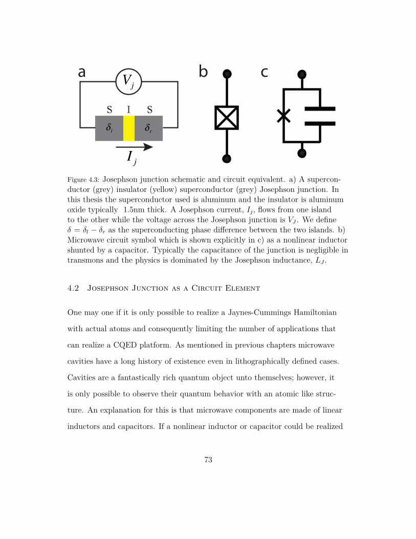
s sI
! l ! r
I j
Vja b c
Figure 4.3: Josephson junction schematic and circuit equivalent. a) A supercon-ductor (grey) insulator (yellow) superconductor (grey) Josephson junction. Inthis thesis the superconductor used is aluminum and the insulator is aluminumoxide typically 1.5nm thick. A Josephson current, Ij, flows from one islandto the other while the voltage across the Josephson junction is VJ . We defineδ = δl − δr as the superconducting phase difference between the two islands. b)Microwave circuit symbol which is shown explicitly in c) as a nonlinear inductorshunted by a capacitor. Typically the capacitance of the junction is negligible intransmons and the physics is dominated by the Josephson inductance, LJ .
4.2 Josephson Junction as a Circuit Element
One may one if it is only possible to realize a Jaynes-Cummings Hamiltonian
with actual atoms and consequently limiting the number of applications that
can realize a CQED platform. As mentioned in previous chapters microwave
cavities have a long history of existence even in lithographically defined cases.
Cavities are a fantastically rich quantum object unto themselves; however, it
is only possible to observe their quantum behavior with an atomic like struc-
ture. An explanation for this is that microwave components are made of linear
inductors and capacitors. If a nonlinear inductor or capacitor could be realized
73

then rich physics in alternative platforms could be developed. Fortuitously, such
a device exists. We begin by looking at the Josephson equations for the current
through, IJ , and voltage across, VJ , a superconducting-insulating-superconducting
barrier:
IJ = I0 sin δ(t) (4.5)
VJ =ℏ2e
δ(t) (4.6)
In equation 4.5, I0 is the critical current of the Josephson junction and δ(t) =
δl − δr is the time dependent phase difference between the two superconducting
sides of the junction. The voltage across the junction, Eq. 4.6, is expressed in
terms of the reduced Planck constant, ℏ, the electron charge, e, and the time
derivative of the phase difference between the two superconducting leads δ(t).
By taking the time derivative of equation 4.5 we express δ(t) as:
IJ = I0 cos δ(t)δ(t) ⇒ δ(t) =IJ
I0 cos δ(t)(4.7)
Using the result for δ(t) the voltage across the junction is:
VJ =ℏ2e
δ(t) =ℏ
2eI0 cos δ(t)IJ (4.8)
We now recognize that equation 4.8 is in the form of an inductance relationship
(Vj ∝ IJ). We will describe the proportionality as the Josephson inductance, Lj,
74

and define this nonlinear inductance as:
LJ =ℏ
2eI0 cos δ(t)(4.9)
A nonlinear inductor is exciting because this could potentially have an an-
harmonic spectrum. Furthermore we note that this inductance is not associated
with a magnetic field. The inductance is due to the kinetic energy of the Cooper
pairs tunneling through the junction. Explicitly this means that the Joseph-
son junction’s inductance is purely kinetic inductance. For this reason, typical
transmon qubits have kinetic inductance fraction of order unity since the induc-
tance of the transmon is primarily due to the Josephson junction.
It is fair to ask at what frequency the Josephson junction self resonates. For
Al-AlOx-Al junctions that have an overlap area of 100nm by 100nm, typical
Josephson inductance values are of order 10nH and from a simple parallel plate
calculation a capacitance of roughly 1fF. This order of magnitude for Joseph-
son inductance and capacitance sets the self resonance of the junction at nearly
50 GHz. To lower the fundamental frequency to the 5-10 GHz range a sim-
ple solution would be to either inductively or capacitively shunt the Joseph-
son junction. A shunting capacitance of 50 fF or shunting inductance of 1.5
µH would bring the resonance of the combined circuit to frequencies in the 5-
10 GHz range. Designing a microwave circuit with 50 fF of shunting capacitance
is easy to achieve; however, 1.5 µH of inductance is a challenging task. Concep-
tually, a single junction shunted by a large capacitor is described as a transmon
[88, 89, 90], and a single junction shunted by a so called super-inductance is de-
75
scribed as a fluxonium [91, 92]. Also, it is worth noting that the transmon and
the fluxonium are both descendants of the original charge qubit–the cooper pair
box [93].
4.3 Circuit Quantization
4.3.1 LC Oscillator
The rules of circuit quantization are treated fantastically well in references [94,
90, 95, 96] and will not be reproduced in full here. For an LC oscillator we can
write its Hamiltonian in terms of the charge on the capacitor, q, and flux through
the inductor, ϕ, as:
HLC =q2
2C+
ϕ2
2L(4.10)
To quantize equation 4.10 the charge now becomes the charge operator, q,
and similarly the flux becomes the flux operator, ϕ which allows one to define
creation, a†, and annihilation, a, operators to realize a quantum harmonic oscil-
lator:
HLC = ℏω(a†a+ 1/2) (4.11)
Where we define the creation, a†, and annihilation, a, of the LC oscillator as:
[a, a†] = 1 (4.12)
ϕ = ΦZPF (a+ a†) (4.13)
q = −iQZPF (a− a†) (4.14)
76
And the zero point fluctuations of the flux and charge are:
ΦZPF =
√ℏZ2
(4.15)
QZPF =
√ℏ
2 Z(4.16)
Finally, the angular frequency, ω, and impedance, Z, are defined in the usual
way as:
ω =1√
LC(4.17)
Z =
√L
C(4.18)
4.3.2 Anharmonic Oscillator: The Transmon
To treat the case of a single Josephson junction shunted by a capacitor we will
modify equation 4.11 by including the Josephson energy and removing the lin-
ear inductance:
HT = ℏωa (a†a+ 1/2)− EJ(cos(ϕ) +ϕ2
2) (4.19)
Where we have defined EJ =I0Φ0
2πas the Josephson energy where I0 is the
critical current of the junction and Φ0 =h
2eis the flux quantum. Expanding
cosϕ and only keep terms related to energy differences gives:
HT = ℏωa a†a− EJ
24ϕ4 +O(ϕ6) (4.20)
77

CLJ
q! !
EJ cos!
a) b)
Figure 4.4: Circuit representation of a transmon. a) The transmon consists of aJosephson junction (square with x) with nonlinear inductance LJ shunted bya capacitor, C. b.)Analogy can be made between a transmon and a quantumrotator [88] and for ϕ ≪ 1 this system realizes an anharmonic oscillator.
Using the definition for ϕ as in equation 4.13 with the caveat that L → LJ
equation 4.20 becomes:
HT ≈ ℏωa a†a− EJ
24Φ4
ZPF (a+ a†)4 (4.21)
Finally by taking only counter rotating terms we realize the simplest form of the
transmon Hamiltonian:
HT ≈ ℏωa a†a− ℏα2a†2a2 (4.22)
In equation 4.22 we have defined ωa = ωa − α and α = EJ
12Φ4
ZPF . The coeffi-
cient α is commonly referred to as the anharmonicity of the transmon with typ-
ical values in the hundreds of MHz. The most faithful description of the anhar-
78

monicity is that it is proportional to the energy difference of the ground state
of the anharmonic oscillator and its first excitation, ℏα = E0 − E1. The ap-
proximation we made in expanding the cosine term of the Josephson junction
is most accurate for a small number of excitations of the transmon. Equation
4.22 can be thought of in terms of a mass spring system with ϕ playing the role
of position and q the role of momentum. The choice of which electrical variable
corresponds to which mechanical variable is arbitrary. However, chosen as such,
the nonlinearity of the junction can be thought of as altering the potential en-
ergy of the system (nonlinear spring constant) rather than the nonlinearity of
the junction serving as a relativistic correction to the mass. In cQED, typically
only the first two energy levels of the transmon are used so equation 4.22 can be
rewritten as a faux two level system with energy levels |g⟩ , |e⟩ as:
HTr = ℏωa |e⟩ ⟨e| (4.23)
Written as a two level system, equation 4.23 suggests that a capacitively shunted
Josephson junction could fulfill the role of a two level system in a Jaynes-Cummings
Hamiltonian.
4.4 Transmon Coupled to Harmonic Oscillator
The previous two sections individually arrived at the quantum Hamiltonians for
electrical circuits. The culmination of that effort is this section where a quan-
tum LC oscillator is coupled to an anharmonic LC oscillator allowing one to
79

create a CQED system with purely electrical circuit elements [97, 98]. For the
case of a transmon coupled to an LC oscillator we can say the total Hamilto-
nian will be a combination of the transmon Hamiltonian, HT , the LC oscillator
Hamiltonian, HLC , and an interaction Hamiltonian, HO:
Htot = HT +HLC +HO (4.24)
To remind the reader, HT is:
HT ≈ ℏωT a†a− ℏα2a†2a2 (4.25)
Likewise, HLC is:
HLC = ℏωr(b†b+ 1/2) (4.26)
The major work of this section is determining the interaction Hamiltonian
which we will initially write in terms of the charge operators for the transmons,
qT , and the charge operator for the LC oscillator, qLC :
HO =qTqLC
Cnet
(4.27)
Where the net coupling capacitance, Cnet is:
Cnet =CCΣ + CΣCC + CCC
CC
(4.28)
80

CLJ C!
2Cc
2Cc
L
Figure 4.5: Circuit representation of transmon coupled to LC oscillator. Thetransmon consists of a Josephson junction (square with x) with nonlinear in-ductance LJ shunted by a capacitor, CΣ is capacitively coupled,CC , to an LCoscillator.
We now rewrite the interaction Hamiltonian in terms of the quantum zero point
fluctuations and raising and lowering operators of each charge operator as:
HO =(−iQT,ZPF (a− a†)
) (−iQr,ZPF (b− b†)
) 1
Cnet
HO =QT,ZPFQr,ZPF
Cnet
(a†b+ ab† − (ab+ a†b†))
HO,rwa =QT,ZPFQr,ZPF
Cnet
(a†b+ ab†) (4.29)
To arrive at equation 4.29 we have taken the rotating wave approximation. We
can rewrite equation 4.29 in an even more suggestive form:
HO,rwa = ℏg(a†b+ ab†) (4.30)
81

With g defined as:
g =1
2√ZTZLCCnet
(4.31)
Now the full Hamiltonian of the coupled transmon and resonator system is:
Htot ≈ ℏωr(b†b+ 1/2) + ℏωT a†a− ℏα
2a†2a2 + ℏg(a†b+ ab†) (4.32)
The above Hamiltonian is a Jaynes-Cummings Hamiltonian provided that we
restrict the transmon to only single photon excitations which is a requirement
routinely met in quantum superconducting circuits. We see all the characteris-
tics necessary. A Hamiltonian term corresponding to cavity excitations, terms
corresponding to an anharmonic oscillator (the most anharmonic oscillator is
a two level system) and finally an interaction term that lets excitations in the
cavity or transmon under go a unitary evolution at rate g where the excitation
is created in one and destroyed in the other. The ‘strong coupling’ regime is en-
tered when interaction strengths are larger than decoherence mechanisms. Ex-
plicitly when g ≫ γT , κr where γT is the decay rate of the artificial atom and κr
is the decay rate of the cavity.
4.4.1 Strong Dispersive Regime
The Jaynes-Cummings like Hamiltonian derived in equation 4.32 can be rewrit-
ten when the detuning between the resonator and the transmon is large com-
pared to the interaction strength (∆ = |ωr − ωT | ≫ g) as (full details of deriva-
82

a
b c
ed
Figure 4.6: Charge based superconducting qubits. a) The original charge basedsuperconducting qubit: the Cooper pair box. b) The offspring of the Cooperpair box are the capacitively shunted Josephson junction, transmon, and c) theinductively shunted Josephson junction, fluxonium. d) and e) are the 3D ver-sions of the transmon and fluxonium which due to their well defined electro-magnetic environment have, at the writing of this thesis, the best coherence andenergy relaxation times of any superconducting qubit.
83

tion see Ref. [99]):
Htot ≈ ℏω′T (A†A+1/2)+ℏω′
r(B†B+1/2)− ℏαT
2A†2A2− ℏαr
2B†2B2−ℏχA†AB†B
(4.33)
In the dispersive limit χ → 2g2
∆, αT → Ec, αr → 0. Equation 4.33 has be-
come a frequent form to represent the coupled resonator and transmon system
which treats the transmon’s modest anharmonicity as a perturbation. A reason
for equation 4.33 being a common form is the reliably long coherence times of
single junction transmons [62]. We can generalize equation 4.33 for an arbitrary
number of modes and to fourth order in the junction flux, ϕ, the general Hamil-
tonian is:
H4 = ℏ∑i
(ωia†a− αi
2a†2a2)− ℏ
∑i,j =i
χija†ab†b (4.34)
Where ωi is the dressed frequency of the mode, αi is the mode anharmonicity,
and χij is the state dependent shift between mode i and mode j.
4.5 Black box quantization
In this final section we will go over a major advancement for single junction
devices, the so called black-box quantization (BBQ) [100] method. Where the
BBQ theory and general approach truly shine is not relying on lumped ele-
ment approximations to predict Hamiltonian parameters such as the anhar-
monicities of modes, their state dependent shift, and higher order corrections
to those terms. For a single junction system in BBQ by knowing the admit-
tance across the junction, Y (ω), one can fully determine the Hamiltonian pa-
84

rameters. The information needed are the poles, Y (ωi) = 0, which correspond
to undressed frequencies and the characteristic impedance at the resonance fre-
quency, Zc,i =√
Li
Ci. The characteristic impedance of the modes can be deter-
mined by using the admittance for a parallel LCR circuit:
Y (ω) = jωCi +1
jωLi
+1
Ri
(4.35)
Taking the derivative of the admittance with respect to angular frequency yields:
Y ′(ω) = j(Ci +1
ω2Li
) (4.36)
We are concerned with the characteristic impedance of the mode on resonance
so we can use ω2i =
1
LiCi
:
Y ′(ω) = 2jC (4.37)
Using Li =1
ω2iCi
the characteristic impedance of the mode on resonance is:
Zc,i =1
ωiCi
(4.38)
Realizing that from equation 4.37 we can write the capacitance Ci on resonance
as:
C =Im[Y ′(ω)]
2(4.39)
85

a b
cω
)] (m
S)
1 2 3
Figure 4.7: Black-box quantization HFSS simulation. a) CAD drawing of two 3Drectangular cavities coupled to a ‘vertical’ transmon. b) Zoom in on faux junc-tion area. In red is a lumped element set to be Lj. In green is the wave portthat allows us to produce c) which is the frequency dependent imaginary part ofthe admittance seen by the junction. Points 1, 2, and 3 correspond to the dif-ferent modes in our system corresponding to the transmon, the low frequencycavity, and the high frequency cavity. By inspection one can clearly see that thehigh frequency cavity will be more linear than the lower frequency cavity andcorrespondingly have a smaller state dependent shift to the transmon.
Finally the characteristic impedance of the mode on resonance in terms of the
poles of the admittance and the slopes of the poles is:
Zc,i =2
ωiIm[Y ′(ωi)](4.40)
Which is fantastic because now by knowing the admittance across the junction
as a function of frequency the Hamiltonian parameters can be fully determined.
86

In practice, one obtains Y (ω) through an electromagnetic simulation (ANSYS’
HFSS was used in this thesis). By using a 2D drawing of the deposited super-
conductor, the junction can be simulated as an imposed boundary condition
with a series inductance of LJ (and if one desires a Cj or Rj). In parallel with
the junction is a port that allows one to measure the imaginary part of the ad-
mittance as a function of frequency as seen by the junction. By knowing the
location of the poles in frequency, the slopes at the poles, and the junction in-
ductance one can readily obtain the Hamiltonian parameters to arbitrary order.
As coherence increases for qubits and cavities, knowing their anharmonicities,
state dependent shifts, and higher order corrections will be crucial for successful
implementations. For each mode we can write its contribution to fourth order in
ϕ as:
Hm = ℏωma†a− ℏαma
†2a2 (4.41)
Where ωm and αm are:
ωm = ω0 − αm (4.42)
αm =e2Z2
c
ℏLj
(4.43)
The above equations are only approximations as found in Ref. [100]. A com-
mon practice is to use QuTIP [101] to diagonalize the full system Hamiltonian.
The circuit designer need only provide the zero crossings of the admittance, the
slope at the zero crossings, and the junction inductance to extract Hamiltonian
parameters from the electromagnetic simulation. Since QuTIP is open source it
87

is quite conceivable that in the near future a function can be added to the ex-
isting database much in the same way there are built in functions for Wigner
functions or Husimi Q functions. The advantage here is it would allow BBQ
to become the industry standard for simulating quantum systems much as the
transmon has become ubiquitous.
A nice observation is that anharmonic modes such as the transmon will have
much smaller slopes than cavity like modes with a very large slope. By know-
ing this coupled with the fact that the state dependent shift between modes is
χij ≈ 2√αiαj, one can quickly look at a plot and have a good sense for what
the order of strength the Hamiltonian parameters are as well as when changing
physical dimensions how that affects Hamiltonian parameters.
88
5Experimental Techniques
This chapter is devoted to the details of the materials, equipment and proce-
dures used in all the experiments in this dissertation. The general framework for
experimental pursuits in the Schoelkopf group is circuit quantum electrodynam-
ics (cQED). In this thesis a cQED experiment is realized with two rectangular
waveguide cavities which have “box” mode resonances coupled to a transmon
89

qubit. These modes are pervasive even in planar structures where these modes
are ignored and hopefully avoided as they potentially serve as another mecha-
nism for decoherence. As the size and complexity of the quantum circuits used
increases so to will the care and design required to preserve coherence.
5.1 Fabrication
5.1.1 Substrates
All fabrication in this thesis is performed on 50mm diameter, c-plane sapphire
substrates. Sapphire is an anisotropic material and the c-plane version specifies
the plane in which wafers are cut from the sapphire ingot. C-plane sapphire has
a uniform dielectric constant along the large surface of the wafer (ϵr,∥ ≈ 9.3) and
a larger dielectric constant perpendicular to the the large surface (ϵr, ⊥ ≈ 11.5).
The early work with stripline resonators was predominately on single side pol-
ished, 480 µm thick sapphire. Eventually, the Schoelkopf group began to only
purchase double side polished, 430 µm sapphire and the stripline experiments
migrated over accordingly. No appreciable changes in device performance were
observed. All transmon fabrication performed in this dissertation was on 50mm
diameter, 430 µm thick, c-plane, double side polished sapphire.
90

5.1.2 Lithography
Striplines
For the fabrication of the stripline resonators a bilayer resist is used for optical
lithography. The bilayer of resist consists of a bottom layer of MicroChem LOR
5A (∼ 480nm thick) and a top layer of MicroChem photoresist S1805 (∼ 500nm
thick). Details on the full procedure are available in appendix A. One thing to
explicitly point out is that adhesion between the sapphire substrate and the first
resist, LOR5A, was found to be inconsistent. After exposing and developing, the
bilayer resist a common occurrence was for the the entire bilayer to be removed
by the development process. To remedy the adhesion issue in subsequent ex-
periments, the sapphire substrate was pretreated with HMDS and adhesion was
no longer an issue. All the optical processing was done using the Heidelberg di-
rect writer. This tool enabled fast turn around of devices and designs since the
“mask” was a file produced by the experimentalist. For the standard configu-
ration, the direct writer can reliably make feature sizes down to a few microns
which is not an issue considering the smallest feature size for the stripline was
of order a few hundred microns. By changing the laser head on the direct writer
features down to ∼ .5 µm can be written but this project did not evolve to the
point of requiring such small features.
91
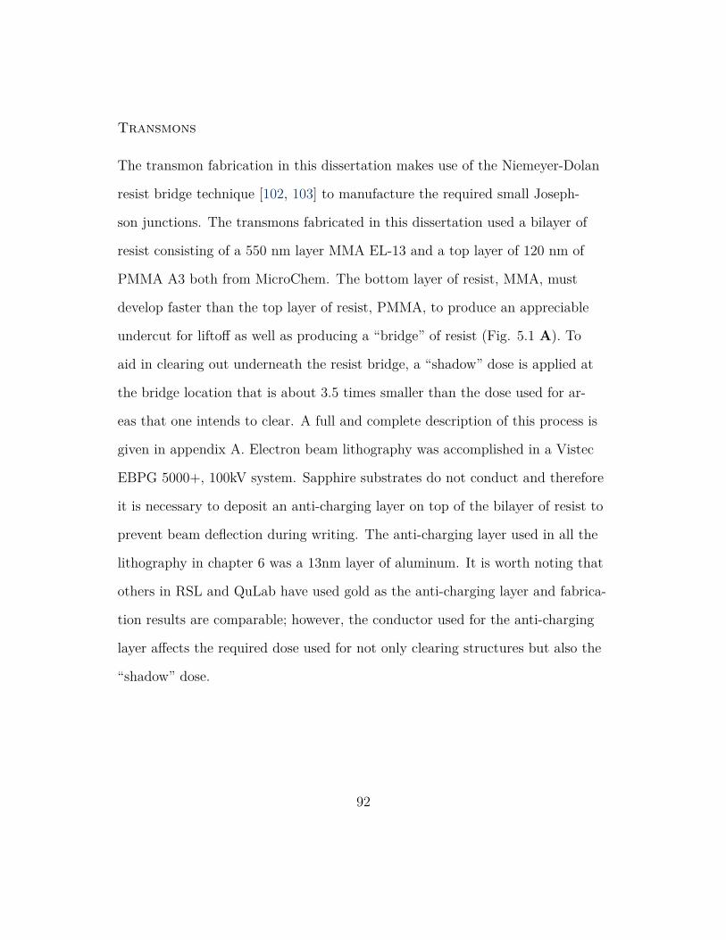
Transmons
The transmon fabrication in this dissertation makes use of the Niemeyer-Dolan
resist bridge technique [102, 103] to manufacture the required small Joseph-
son junctions. The transmons fabricated in this dissertation used a bilayer of
resist consisting of a 550 nm layer MMA EL-13 and a top layer of 120 nm of
PMMA A3 both from MicroChem. The bottom layer of resist, MMA, must
develop faster than the top layer of resist, PMMA, to produce an appreciable
undercut for liftoff as well as producing a “bridge” of resist (Fig. 5.1 A). To
aid in clearing out underneath the resist bridge, a “shadow” dose is applied at
the bridge location that is about 3.5 times smaller than the dose used for ar-
eas that one intends to clear. A full and complete description of this process is
given in appendix A. Electron beam lithography was accomplished in a Vistec
EBPG 5000+, 100kV system. Sapphire substrates do not conduct and therefore
it is necessary to deposit an anti-charging layer on top of the bilayer of resist to
prevent beam deflection during writing. The anti-charging layer used in all the
lithography in chapter 6 was a 13nm layer of aluminum. It is worth noting that
others in RSL and QuLab have used gold as the anti-charging layer and fabrica-
tion results are comparable; however, the conductor used for the anti-charging
layer affects the required dose used for not only clearing structures but also the
“shadow” dose.
92

A B
DC
“bridge”
substrate
substrate
substrate
substrate
Figure 5.1: Double Angle Dolan Bridge Deposition. In all cartoons, green trape-zoids are previously deposited superconducting material that forms the planarresonator or capacitive pads of the transmon. In brown is the MMA resist whilethe top yellow layer is the PMMA that forms the “bridge”. A Aluminum, navy,deposition at first angle. B Oxidation, orange, of deposited aluminum. C Alu-minum, navy, deposition at a second angle producing an overlap which formsthe Josephson junction. D Final oxidation of the Josephson junction in a con-trolled environment.
93

5.1.3 Deposition and Dicing
Striplines
All deposition for aluminum stripline resonators were done in the Plassys elec-
tron beam evaporator. Depositions were done at a 0 degree angle with respect
to the normal at a rate of 1 nm/s for a thickness of roughly 200nm. Full wafer
liftoff was done with the sample side facing down in acetone at 75 C for at least
an hour (covered), or in NMP at 90 C for at least an hour (covered). Once com-
plete the wafer was coated with S1827 as a protective layer for dicing. It was
found, that chips diced to a width of 1 mm were not robust and prone to break-
ing. However, chips were substantially more robust when diced to widths of 1.2
mm or larger. This minimum width was the driving force behind the stripline
chip widths used in chapter 3.
Transmons
All Josephson junction depositions done in this dissertation were in the Plassys
electron beam evaporator. For the shadow evaporation process two angles are
used and for electrodes of different widths the layering order will alter the Joseph-
son inductance of the device. That is why it is necessary to align the wafer to
the deposition system as well as possible before beginning deposition. Once
fully setup the Plassys will pump down to the 10−8 Torr range before deposi-
tion. The first step is a brief titanium sweep to further lower the pressure. A
critical first step for depositions done on sapphire is an ion- beam cleaning step
94

with an Anatech argon ion gun operating at 250 V for 30 s. The first angle de-
posited is 25 nm of aluminum at a 0 angle with respect to the normal, followed
by an oxidation step of 15 Torr of oxygen for 12 minutes (aluminum has a self
limiting oxide layer so the time duration need not be exact to 12 minutes), a
second deposition of 60nm of aluminum at an angle of 35, and finally another
oxidation at 3 Torr for ten minutes so the final aluminum oxide can be grown
under controlled conditions.
Once finished all handling of the wafer and future devices must be done when
fully grounded and all wafers and devices in a static dissipative container. Joseph-
son junctions are susceptible to static shock which will ruin the junction and
undermine all the work done in creating it. The next step is to lift off the junc-
tions in either acetone at 75 C (covered) for at least an hour or in NMP at 90 C
for at least an hour. Once fully lifted off and cleaned, the wafer must be coated
with S1827 as a protective layer for dicing.
5.2 Sample Holders
5.2.1 Striplines
The first generation stripline holder in chapter 3 were machined in 6061 alu-
minum which is roughly 95% aluminum. However, the second generation stripline
holders were machined from extruded bars (ingots tend to have air pockets
that ruin mill bits and cause the machine shop to be unhappy) of 4N aluminum
(99.99% aluminum) purchased through Laurand Associates. The holders were
etched according to the process described in appendix A which in Ref. [58] was
95

shown to improve the internal quality factor of aluminum waveguide cavities.
5.2.2 Cavities
In chapter 6 a two rectangular waveguide cavity sample, which was antenna
coupled to a transmon, was machined from high purity (4N) aluminum. The
cavities were then etched following the procedure in appendix A which was
shown in Ref. [58] to improve internal dissipation of aluminum cavities.
5.3 Experimental Setup
5.3.1 Dilution Refrigerator
The heart of the experiments done in quantum computing and information with
superconducting circuits is the dilution refrigerator. Further solidifying that
analogy is the distinctive 1 Hz beat of the pulse tube which when stopped (even
intentionally) draws a concerned look from all experimentalists in the room. All
experiments done in chapter 3 and chapter 6 were performed in cryogen free di-
lution refrigerators which only require electricity, cooling water, and compressed
air for normal operation (with the hidden caveat of requiring liquid nitrogen
to refill the external cold trap once a week). In chapter 3 all experiments were
performed in an Oxford Triton 200 with a base temperature of 20 mK. All ex-
periments performed in chapter 6 were performed in a Vericold (acquired by
Oxford) dilution refrigerator with a base temperature of 20 mK. The Vericold
is a bit unusual in that its helium 3 and 4 mixture is over 1 bar where as the
Oxford systems typically have their mixture in the .6-.7 bar range.
96

5.3.2 Vericold Wiring and Filtering
This section is devoted to the description and explanation of the experimental
setup used in chapter 6.
5.3.3 Cavity Filtering
The general goal with our filtering is to prevent unwanted and unintended pho-
tons from entering in our device and ruining performance. On the input side
we attenuate at the “4 K” stage with -20 dB cryogenic safe attenuators and
at the base plate with -30 dB attenuators. For most applications we only need
a few photons in the 5-10 GHz range— a noteworthy exception is the Jaynes-
Cummings high power readout discussed in section 5.5.2 — so the attenuation
on the input side is fine as long as the dilution refrigerator has enough cooling
power to handle the microwave power dissipated by the attenuators on the base
plate. Where things are a bit trickier is on the output side because the signal
carrying precious quantum information will also only be a few photons for a dis-
persive readout (section 5.5.1).
Circulators and Isolators
On the output side between the HEMT at “4 K” and the sample are two PAMTECH/Quinstar
3-12 GHz isolators. These isolators provide -20 dB of directionality to our mi-
crowave signals, so two isolators in series, as in figure 5.2 gives -40 dB of isola-
tion from the HEMT at the “4 K” stage. It has been postulated that -40 dB of
isolation is inadequate and one of the newer Schoelkopf lab fridges was outfitted
97
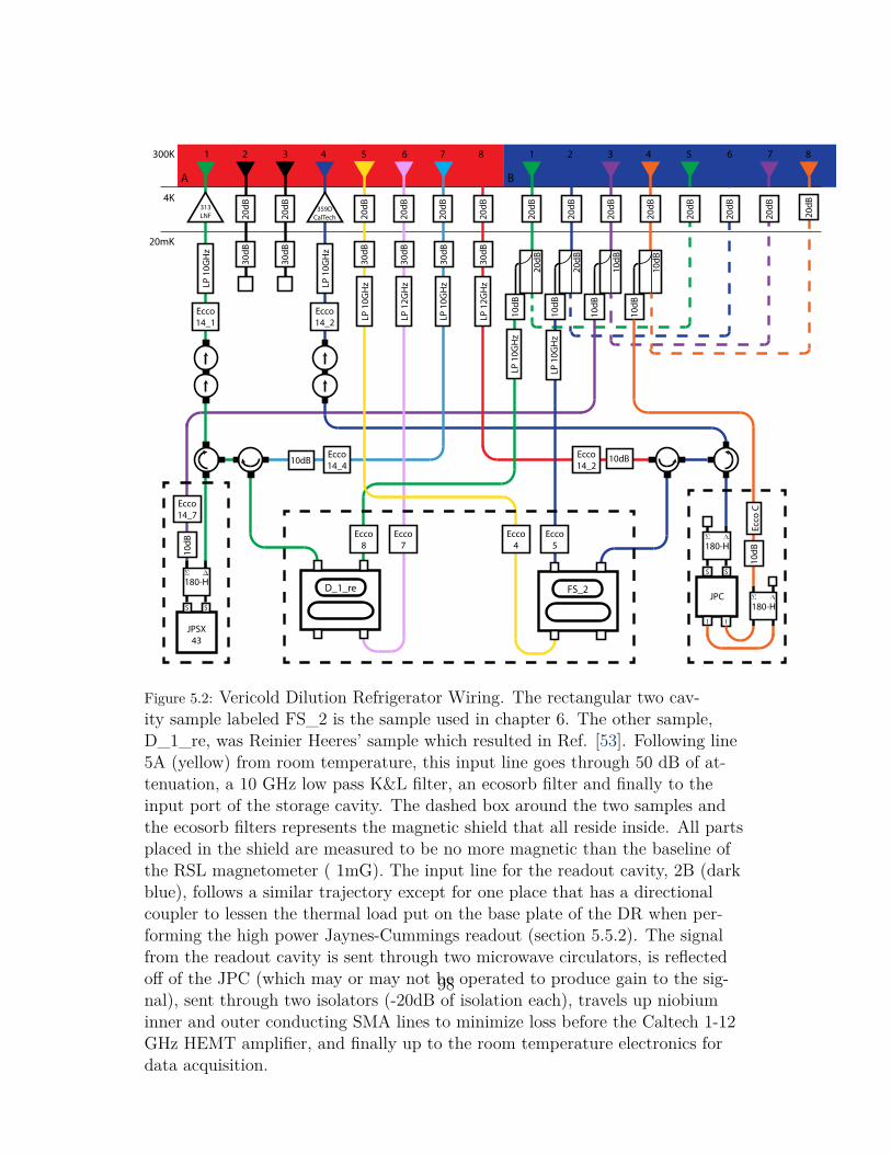
300K
4K
20mK
1 2 3 4 5 6 7 8 1 2 3 4 5 6 7 8
20dB
20dB
20dB
20dB
20dB
20dB
20dB
20dB
20dB
20dB
20dB
20dB
20dB
20dB359D
CalTech
30dB
30dB
30dB
30dB
30dB
30dB
10dB
10dB
10dB
LP 1
2GH
z
LP 1
0GH
z
Ecco5
A B
LP 1
0GH
z
LP 1
0GH
z
LP 1
0GH
z
20dB
10dB
20dB
10dB
10dB
LP 1
2GH
z
LP 1
0GH
z
Ecco8
D_1_re
Ecco7
10dB 10dB
Ecco4
FS_2
313LNF
LP 1
0GH
z
JPSX43
180-H
S S
10dB
Ecco14_7
Ecco14_2
JPC
180-H
180-H
Ecco
C10
dB
S S
I I
Ecco14_1
Ecco14_2
Ecco14_4
Figure 5.2: Vericold Dilution Refrigerator Wiring. The rectangular two cav-ity sample labeled FS_2 is the sample used in chapter 6. The other sample,D_1_re, was Reinier Heeres’ sample which resulted in Ref. [53]. Following line5A (yellow) from room temperature, this input line goes through 50 dB of at-tenuation, a 10 GHz low pass K&L filter, an ecosorb filter and finally to theinput port of the storage cavity. The dashed box around the two samples andthe ecosorb filters represents the magnetic shield that all reside inside. All partsplaced in the shield are measured to be no more magnetic than the baseline ofthe RSL magnetometer ( 1mG). The input line for the readout cavity, 2B (darkblue), follows a similar trajectory except for one place that has a directionalcoupler to lessen the thermal load put on the base plate of the DR when per-forming the high power Jaynes-Cummings readout (section 5.5.2). The signalfrom the readout cavity is sent through two microwave circulators, is reflectedoff of the JPC (which may or may not be operated to produce gain to the sig-nal), sent through two isolators (-20dB of isolation each), travels up niobiuminner and outer conducting SMA lines to minimize loss before the Caltech 1-12GHz HEMT amplifier, and finally up to the room temperature electronics fordata acquisition.
98
with three isolators in series for -60 dB of isolation. No definitive answer exists
for whether or not -60 dB of isolation is necessary though an argument can be
made in its favor.
In figure 5.2 two PAMTECH/Quinstar 8-12 GHz circulators are used with a
Josephson parametric converter (JPC). The two circulators allow for reflection
to occur off of the JPC (with or without gain). One port on the first circula-
tor isn’t essential and this circulator could be replaced with an isolator. How-
ever, the superfluous port is diagnostically useful for measuring and characteriz-
ing the JPC independent of the sample. For a circulator to operate effectively,
all incoming ports must be matched. In figure 5.2, the -10 dB attenuator is at-
tached to one circulator to fix the mismatch in impedance between the ecosorb
filter and the circulator. Without the attenuator the circulator does not main-
tain its reverse isolation.
Ecosorb Filters
The ecosorb filters in this thesis serve the purpose of attenuating signals above
20 GHz. The idea behind these filters is to make a transmission line that is
filled with a dielectric that is not very lossy in the 5-10 GHz range but whose
loss increases as a function of frequency and is very lossy at high frequencies.
In this thesis ecosorb filters filled with CR-110 were used to produce the mi-
crostrip version of ecosorb filters. A thorough investigation into the different
types of ecosorb was undertaken by Geerlings and is available in his thesis [104].
It would seem that the coaxial version of the ecosorb filters is preferable due to
99

its ability to better impedance match to the SMA lines.
K&L Cavity Filters
The K&L cavity filters serve the purpose of rejecting signals from roughly 10-
20 GHz. Any resonator will have multiple higher modes and 3D rectangular
cavities in particular have a multitude higher modes. Typically the fundamen-
tal mode of the readout cavity is designed to be around 9 GHz and any higher
mode is above 10 GHz. K&L filters prevent noise at the higher mode frequen-
cies from entering the cavity and hopefully minimize the amount of photon shot
noise dephasing experienced by the qubit [63].
Nonmagnetic Components
A more recent point of emphasis in the Schoelkopf group is using measurably
nonmagnetic components. The room temperature magnetometer used for all
measurements is a 3 axis Bartington Mag-03 (basic model) that can reliably
measure down to ≲ 1 mG. Fully enclosed copper SMA cables are used on the
input and output of the sample with hand formable cables being reserved for
room temperature setup. All wiring, SMA connectors, and other components
are nonmagnetic to the level that can be measured. All components are mea-
sured in a room temperature and are only used inside the sample magnetic
shield if the component is not measurably magnetic. Although somewhat te-
dious to spend an afternoon measuring everything that will be used near the
sample the payoff was that devices in the Vericold seemed to have a substan-
100

tially smaller excited state population after this change.
Magnetic Shielding and Infrared
The magnetic shielding used in the experiments of chapter 6 was initially de-
sign by Gerhard Kirchmair. The design is a cylinder made of cryoperm shielding
that is then capped with another cryoperm shield. The shield and cap lock into
one another and both are thermally heat sunk. Slight variations in size have
progressed over the years. The Vericold dilution refrigerator has the smallest
usable sample space and its magnetic shield is small compared to what is used
in other Triton systems especially the newer Triton systems which have a large
volume that can be connected to the base plate. In the Vericold, both samples
were at the very bottom of the magnetic shield and the space above the samples
was used for ecosorb filters. Also, inside the magnetic shield is a copper sheet
that has been covered with ecosorb and is thermally heat sunk to the baseplate.
The copper sheet is to be an absorber of any stray infrared photons that make
it into the magnetic shield.
5.3.4 Heterodyne Measurement Setup
All of the quantum measurements performed in chapter 6 used a microwave,
heterodyne interferometer (Fig. 5.3). By expanding previous implementations
of heterodyne detection in the Schoelkopf group the microwave interferometer is
less susceptible to drifts in the experimental setup.
The pulse generation was accomplished with a Tektronix AWG 5014C with
101
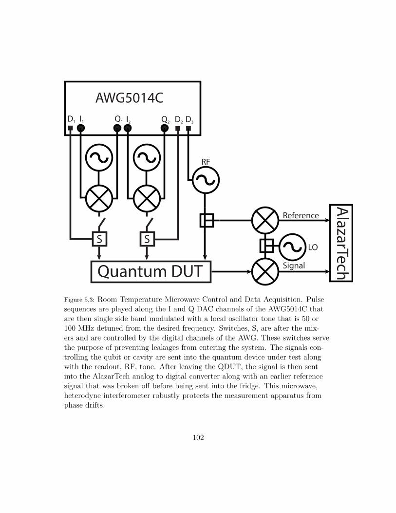
I1 Q1 I2 Q2
AWG5014C
S S
D1 D2 D3
Quantum DUT
AlazarTech
Reference
Signal
LO
RF
Figure 5.3: Room Temperature Microwave Control and Data Acquisition. Pulsesequences are played along the I and Q DAC channels of the AWG5014C thatare then single side band modulated with a local oscillator tone that is 50 or100 MHz detuned from the desired frequency. Switches, S, are after the mix-ers and are controlled by the digital channels of the AWG. These switches servethe purpose of preventing leakages from entering the system. The signals con-trolling the qubit or cavity are sent into the quantum device under test alongwith the readout, RF, tone. After leaving the QDUT, the signal is then sentinto the AlazarTech analog to digital converter along with an earlier referencesignal that was broken off before being sent into the fridge. This microwave,heterodyne interferometer robustly protects the measurement apparatus fromphase drifts.
102
a 1 GS/s digital to analogue converter. The signal, typically modulated at 50
or 100 MHz, is then fed into a microwave mixer along with a 5-10 GHz local
oscillator tone which is single sideband modulated to achieve the desired pulse
shape at the desired frequency. The typical local oscillator used in chapter 6
was a Vaunix LMS-802 generator. For frequency sweeps an Agilent MSG series
microwave generator was used. Measurements are recorded with an analog-to-
digital converter using the AlazarTech. A full schematic of the setup used in
chapter 6 is in figure 5.3.
5.4 Cavity Measurement Techniques
5.4.1 Transmission
All cavity measurements performed in chapter 3 measured the magnitude squared
of S21 in transmission with a vector network analyzer (VNA) where ports 1 and
2 are the input and output ports of the cavity. For the stripline measurements
the two ports were designed to be symmetric so it is arbitrary which port is la-
beled 1 versus 2. A key relation used in chapter 3 was the extraction of the cou-
pling quality factor based on room temperature measurements of the stripline
resonators. The following is a derivation that relates the coupling quality factor
to the total quality factor assuming symmetric coupling. Another assumption is
that the coupling quality factor is much larger than the internal quality factor.
For room temperature measurements of aluminum stripline resonators the inter-
nal quality factors were ∼ 20 whereas coupling quality factors were investigated
all above 103.
103

Transmission Coupling Quality Factor–Symmetric
We define the power applied to port 1 as compared to the powered received to
port 2 in terms of the scattering matrix element as:
|S21|2 =P2
P1
(5.1)
On resonance |S21|2 is defined as the insertion loss of the device. We will say
that the the resonator will have the standard voltage and current relation:
I = V Gtot (5.2)
We can calculate the input power as:
P1 =I2
4G1
(5.3)
The output power will like wise be:
P2 =I2
G2tot
G2 (5.4)
104
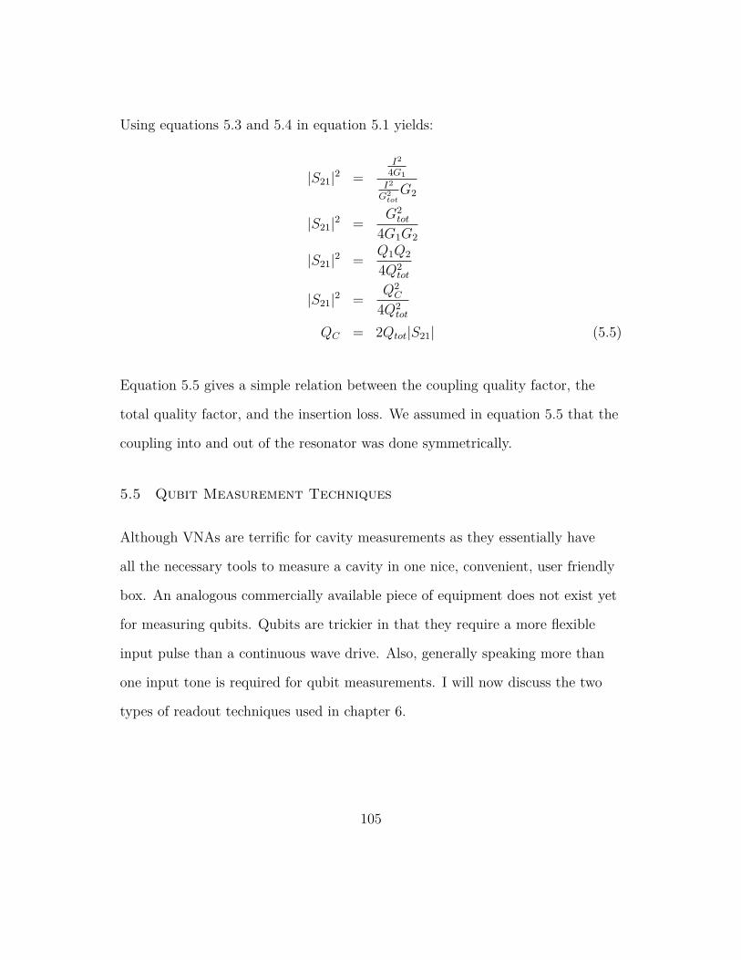
Using equations 5.3 and 5.4 in equation 5.1 yields:
|S21|2 =I2
4G1
I2
G2totG2
|S21|2 =G2
tot
4G1G2
|S21|2 =Q1Q2
4Q2tot
|S21|2 =Q2
C
4Q2tot
QC = 2Qtot|S21| (5.5)
Equation 5.5 gives a simple relation between the coupling quality factor, the
total quality factor, and the insertion loss. We assumed in equation 5.5 that the
coupling into and out of the resonator was done symmetrically.
5.5 Qubit Measurement Techniques
Although VNAs are terrific for cavity measurements as they essentially have
all the necessary tools to measure a cavity in one nice, convenient, user friendly
box. An analogous commercially available piece of equipment does not exist yet
for measuring qubits. Qubits are trickier in that they require a more flexible
input pulse than a continuous wave drive. Also, generally speaking more than
one input tone is required for qubit measurements. I will now discuss the two
types of readout techniques used in chapter 6.
105

a b
χ
Readout spectrum Dispersive readoutqubit spectrum
fCe fC
g
Frequency
Am
plitu
de
Figure 5.4: Dispersive Readout. A conceptual cartoon depiction of the underlyingprinciples of the dispersive readout. By having a strong, dispersive interactionbetween the qubit and cavity the frequency of the cavity is dependent on thestate of the qubit. a The frequency of the cavity is resolvablely different whenthe qubit is in the ground state, blue, or in the excited state, red. b Having thereadout tone applied to the cavity frequency corresponding to the qubit in theground state, double arrow in a, allows transmission through the cavity whenthe spectroscopic tone is not resonant with the qubit. When the spectroscopictone is applied on resonance with the qubit, the cavity frequency changes andthe observed transmitted signal drops.
106
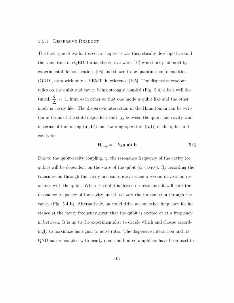
5.5.1 Dispersive Readout
The first type of readout used in chapter 6 was theoretically developed around
the same time of cQED. Initial theoretical work [97] was shortly followed by
experimental demonstrations [98] and shown to be quantum non-demolition
(QND), even with only a HEMT, in reference [105]. The dispersive readout
relies on the qubit and cavity being strongly coupled (Fig. 5.4) albeit well de-
tuned, g
∆< 1, from each other so that one mode is qubit like and the other
mode is cavity like. The dispersive interaction in the Hamiltonian can be writ-
ten in terms of the state dependent shift, χ, between the qubit and cavity, and
in terms of the raising (a†,b†) and lowering operators (a,b) of the qubit and
cavity is:
Hdisp = −ℏχa†ab†b (5.6)
Due to the qubit-cavity coupling, χ, the resonance frequency of the cavity (or
qubit) will be dependent on the state of the qubit (or cavity). By recording the
transmission through the cavity one can observe when a second drive is on res-
onance with the qubit. When the qubit is driven on resonance it will shift the
resonance frequency of the cavity and thus lower the transmission through the
cavity (Fig. 5.4 b). Alternatively, on could drive at any other frequency for in-
stance at the cavity frequency given that the qubit is excited or at a frequency
in between. It is up to the experimentalist to decide which and choose accord-
ingly to maximize his signal to noise ratio. The dispersive interaction and its
QND nature coupled with nearly quantum limited amplifiers have been used to
107

demonstrate a variety of novel quantum phenomena [106, 107, 46, 108, 109, 110,
111, 112, 113, 114].
5.5.2 Jaynes-Cummings Readout
An alternative mechanism to readout the state of a qubit was discovered in 2010
using the Jaynes-Cummings interaction between an anharmonic oscillator and
a cavity [115]. The unique observation is as follows, by driving very hard at the
bare cavity frequency the cavity can fully decouple from the qubit and its high
power peak can be resolved. The unique observation is that by having the qubit
excited less power is required to drive the cavity to its bright state. This gives
a very non-QND method to measure the state of the qubit. The trade off for
non-QND measurements is the robust, high fidelity single shot readout for this
method.
We begin by describing the observed cavity frequency as a function of power.
At low powers which correspond to n ≈ 1 one would observe the cavity at its
dressed frequency due to the quantum coupling to the qubit as is described
in chapter 4. However, as the drive power applied to the readout cavity is in-
creased the frequency of the cavity will begin to lower due to the inherited Kerr
nonlinearity from the qubit. At some point when the applied power to the cav-
ity is large enough no longer will one have a cavity response. To put things col-
loquially the cavity spectroscopically disappears. The innovation by Reed was
to not be dismayed by the lost cavity response and to continue to increase the
applied power to the cavity. At some very high power the cavity resonance will
108

Qubit ground state
100
80
60
40
20
0
Sign
al (m
V)
86420-2-4Readout power (dBm)
Qubit excited state
Figure 5.5: Jaynes-Cummings Readout. The observation of Ref. [115] was thatfor different qubit states, when the readout cavity is driven at its undressed res-onance the cavity will decouple from the qubit at different drive powers. In blueis the digitized readout signal as a function of drive power applied to the read-out cavity at a fixed frequency when the qubit is in the ground state. In red isthe digitized signal for the case when the qubit is in the excited state. When inthe excited state the qubit requires less power to make the readout cavity “gobright”. By using a power between 1 and 3 dBm a relatively large signal willresult from the measurement.
109

reappear. This frequency can be thought of as the uncoupled cavity frequency
and it occurs much lower in frequency that the low power resonance. The cavity
response at high powers is very strong and is why it is occasionally referred to
as a bright state.
A further unique observation by Reed, was that one can use this unique bright
state as a readout mechanism. By projecting a quantum state on to a classi-
cal output this readout scheme has a robust, high single shot fidelity for a wide
array of parameters. To readout the qubit state as in Fig. 5.5, one finds that
the power required to cause the cavity to go bright when the qubit is in the ex-
cited state is less than the power required to make the cavity go bright when
the qubit is in the ground state. The disadvantages to this readout mechanism
is that it is not QND and requires long dead time to reset the system. Typically
for a cavity with a lifetime of a few microseconds one would need to set the rep-
etition rate of the experiment to a few milliseconds. The optimal choice for a
repetition rate is one that does not negatively impact the coherence nor the per-
formance of the quantum device under test.
110

6Cavity State Reservoir Engineering
6.1 Introduction
In this chapter we undertake the challenge of taming active quantum systems.
In the absence of drives a quantum system will naturally decay to thermal equi-
librium with its environment. Regardless of the physical system, the thermal
equilibrium state is singular and, at best, serves to initialize the quantum sys-
111

tem to its ground state. A major obstacle for quantum information and quan-
tum computation is that the quantum states used are non-equilibrium states.
These non-equilibrium states persistently dissipate entropy to the environment,
losing their information. Two well developed methods in combating entropy loss
from a quantum system are measurement with external feedback or through
reservoir engineering.
6.1.1 Measurement with External Feedback
In this section we introduce a well studied method for controlling active systems–
measurement with external feedback. Theoretical ideas for sequential unitary
operations to control open quantum systems predate quantum computing [116];
however, quantum information did inspire further development [117, 118]. Early
experimental work lacked the ability for real-time external feedback [119, 120,
121, 122] yet still showed great promise. Proposals for cavity QED protocols
that stabilize photon number states, Fock states, required external feedback
[123, 124]. Advances in technology allowed a series of experiments by the Haroche
group [125, 126, 127] to stabilize Fock states in a microwave cavity through re-
peated measurement and real-time feedback. Other fields have also made use of
measurement with real-time feedback by stabilizing a mixed state of two cesium
atoms [128], or steering a nuclear spin to a target state through ancilla measure-
ments [129].
The superconducting quantum circuit community has been quite active in
implementing real-time feedback on quantum systems. Much work has been de-
112

veloped in stabilizing Rabi oscillations of a qubit [107, 130, 131]. In ref. [131]
Rabi oscillations were stabilized by suppressing measurement induced dephasing
on the qubit whose approach was inspired by worked in trapped ions [132]. In
addition, weak measurements and feedback enabled teams to design arbitrary
quantum trajectories [133]. The ground state of a qubit was stabilized through
a series of weak measurements and feedback [110]. Finally, much work has been
invested in the generation [134] and stabilization [111, 112] of an entangled sys-
tems.
Quantum computation and quantum information in particular is interested
in the control and stabilization of quantum systems [135, 20, 22]. In the mea-
surement with real-time external feedback approach high fidelity gates of one
and two qubit rotations are required on the physical qubits so that they may be
concatenated to form a logical qubit [22]. A well known example is the seven
qubit Steane code [20]. In the Steane code the state of a single qubit can be
protected through a series of ancilla measurements that identify bit flip errors
as well as phase errors. The Steane code is attractive because it can be con-
catenated to other seven qubit Steane codes increasing the redundancy so as
to achieve a fault tolerant quantum state. The Steane code serves as a proof of
principle that quantum errors can not only be measured and corrected but also
that these codes can be concatenated to lessen the demands on the individual
physical qubits. Measurement and feedback has been expounded on in great de-
tail in for instance [22]. A major draw back to the aforementioned methods for
the stabilization of logical qubits is the exponentially increasing requirements
113
for physical qubits to serve as an ancilla system to stabilize a logical qubit state.
Since the aforementioned quantum error correcting codes have tremendous
resource demands on the experimentalist two distinct approaches with more fa-
vorable requirements for the control of open quantum systems with supercon-
ducting circuits have come into favor. The first approach by the Yale group, is
a cavity centered architecture for quantum computing with ‘cat’ states of cavi-
ties [136]. This approach seeks to use coherent devices with vast Hilbert spaces,
cavities [58, 137], to realize logical qubit states for fault tolerant computation.
On the experimental front repeated quantum non-demolition allowed real-time
monitoring of the error syndrome [108] which is photon number parity switch-
ing. Repeated measurements with feedback were used in the same setup to pro-
duce an entanglement between a discrete variable system, artificial atom, and a
continuous variable system, cavity, [113]. Additionally, proof of principle cavity
manipulations have been demonstrated [53] which have theoretically been shown
theoretically to serve as a universal set of unitary operations [54]. Future work
is needed in demonstrating high fidelity cavity manipulations. For instance, it
has yet to be experimentally demonstrated that a high fidelity gate can be per-
formed on a cavity transforming it from one logical state to another or putting
it into an arbitrary superposition of both states.
A second proposal to control active quantum systems is a so called surface
code[138, 139, 140, 141, 142] which has potentially more favorable requirements
for the number of physical qubits per logical qubits than concatenating Steane
codes. A fraction of the superconducting quantum circuit community has grav-
114

itated towards this particular implementation of measurement and feedback
scheme in part due to it being a cast as 2D code which, at least conceptually,
has the feel of a planar architecture. The surface code requires nearest neighbor
only interactions between physical qubits. In the 2D fabric of physical qubits
some qubits are data qubits and other qubits serve the purpose of detecting er-
ror syndromes. Through a series of amplitude and phase rotations of the phys-
ical syndrome qubits, a logical qubit state can be prepared from the underlying
physical data qubits. Pursuits are underway at Google (formerly University of
California at Santa Barbara) [143, 109], and IBM [144, 114]. The number of
physical qubits required for a logical qubit is still large (102 − 104) [142] and de-
pends strongly on the underlying coherence properties of each physical qubit.
With increased coherence the number of physical qubits required per logical
qubit decreases. Major advances in the coherence of superconducting qubits are
still required for this codes to be realized with a reasonable number of qubits
and the accompanying fast electronics to control this large quantum system.
Furthermore a fault tolerant quantum computer requires many logical qubits
which just serves to underscore the necessity for continued advances in qubit
coherence for this scheme to be feasible. In terms of implementation, each phys-
ical qubit as well as each logical qubit requires high fidelity single and two qubit
gates.
Any approach that involves conditioning on an ancillary system for external
feedback must overcome any latency. For instance, issues associated with con-
verting quantum information into classical bits, performing state estimate cal-
115

Reservoir
DrivenSystem
! target
Time EvolutionEngineeredInteraction
Figure 6.1: Conceptual schematic of reservoir engineering. The driven system (ei-ther CW or pulse) must have an engineered, intentional coupling to the environ-ment such that as it evolves in time it reaches the target state.
culations on classical information, and then implementing the necessary gates
to correct bit flip and phase errors of the many body quantum state are all out-
standing challenges. All of these concerns must be minimized for protocols re-
quiring measurement and real-time feedback to be successfully implemented.
6.1.2 Quantum Reservoir Engineering
An alternative approach to active quantum systems is quantum-reservoir engi-
neering (QRE) [145, 146, 147, 148, 149] which harnesses persistent, intentional
coupling to the environment as a resource. Although it is common for QRE
proposals to involve continuous wave drives, proposals [150] as well as experi-
mental implementations [151] that use pulsed or stroboscopic drives exist. Both
measurement with external real-time feedback as well as QRE require entropy
removal yet only QRE employs environmental losses as a crucial part of their
protocols. QRE does not require an external feedback with calculation since
the Hamiltonian interactions are designed a priori to determine the final state
116

avoiding uncertainty in the quantum-classical interface. In addition, QRE is less
susceptible to experimental noise [152] and in some cases thrives in a noisy envi-
ronment [153].
QRE is not as well known as other schemes to undermine persistent entropy
loss yet a few implementations exist in superconducting circuits. Qlab demon-
strated a QRE protocol in a cQED environment using a single qubit coupled
to a fast cavity [99]. The protocol of choice was the double drive reset of pop-
ulation, DDROP. DDROP was used to cool a qubit that without DDROP in
steady state had a residual excited state population of about 10%. DDROP
was able to reduce the excited qubit population to ≲ 1% thus offering substan-
tial cooling to the anomalous heat source as well as providing a reset for the
qubit. A second example from Qlab was based on a recent proposal [154] that
stabilized a Bell state between two superconducting artificial atoms [155]. The
aforementioned experimental work was published in tandem with work from the
Wineland group at NIST [156] that also used QRE to stabilize a Bell state but
did it in a trapped ion setup. Autonomously stabilizing a Bell state between
two qubits is impressive in it of itself. What makes this all the more impressive
is the relatively small number of parts required to produced a stabilized Bell
state in contrast to a parity measurement based protocol [111]. A final example
from Qlab is recent work [157] that stabilizes a manifold of a cavity. Other pro-
posals exist from the Yale group to stabilize the even ‘two cat’ state of a cavity
through a QRE protocol [158], implement a 3 qubit bit flip error correction code
[159], or to realize a cat code based computation [160].
117
Other examples of QRE in superconducting circuits include work from UC
Berkley where an arbitrary superposition between the ground and excited states
of the qubit was stabilized [161]. Theoretical work from McGill uses QRE to
create a quantum limited amplifier that does not have a gain-bandwidth prod-
uct [162]. This work has recently been expanded [163] to include directionality
so that an experimental implementation would not require lossy components
connecting to circulators. Additionally, theoretical work from Princeton ex-
ists in the remote entanglement of spatially separated qubits [164]. The last
QRE proposal to mention is one that stabilized a one phonon Fock state of an
optomechanical system [165]. Although, the protocol in ref. [165] results in a
exactly one excitation the QRE protocol is achieved through vastly different
means than the protocol that will be presented in this chapter.
It has been shown theoretically that QRE is in principle not a limited to
what state one can stabilize in that theoretical work exists that proves any pure
quantum state can be arrived at through a QRE protocol [147]. Additionally,
theoretical work exists [166] that demonstrates that a scheme based on mea-
surements and feedback on an ancillary system can be transformed to a QRE
protocol. It is for these reasons that QRE is a beneficial approach to controlling
active quantum systems as well as being useful for quantum computing.
6.2 Fock State Stabilization Protocol
We now introduce the major focus of this chapter–stabilizing Fock states of a
microwave cavity through quantum reservoir engineering. We intend to have
118

this investigation in QRE be a fruitful endeavor in understanding driven dissi-
pative systems, specifically as applied to cavity modes since the quantum com-
puting paradigm of the Yale group is the cavity centric Cat Code architecture
[136]. We view stabilizing Fock states as a proof of principle for specific cavity
state stabilization through QRE. Stabilizing Fock states appears to be concep-
tually, theoretically, as well as less resource intensive than the stabilization of
a superposition states in a cavity or the stabilization of entangled cavity modes
such as entangled cat states.
Shown in Fig. 6.2(b) is a QRE protocol that stabilizes Fock states in a mi-
crowave cavity that for the remainder of this chapter we will refer to as the stor-
age cavity. Fig 6.2 is drawn with the drives applied so as to stabilize a one pho-
ton Fock state in the storage cavity. This protocol which we will refer to as the
Fock State Stabilization Protocol (FSSP) is conceptually similar to DDROP
[99]. Later in the chapter we will present results demonstrating that we stabilize
the vacuum state of the storage cavity as well as the first Fock state.
Due to the anharmonicity of the storage cavity, a CW drive, ΩS, can be ap-
plied to the fs,0→1 transition (Fig. 6.2(a) left). This drive is an induced Rabi
rate between vacuum and a one photon Fock state. Concurrently, with ΩS, a
drive with strength ΩC is applied detuned by a cross-Kerr from the cooling cav-
ity (Fig. 6.2 (a) right). This drive is resonant provided that there is exactly one
photon in the storage cavity (Fig. 6.2(b)). Once resonant, the conditional drive
displaces the cooling cavity to a coherent state determined by the amplitude of
the drive. When a photon decays from the storage cavity ΩC, is no longer reso-
119

(n +1)!!scn!!sc(n !1)!!sc
a
b
κc
Cooling cavity Cooling cavity Storage cavityStorage cavity
1,0
. . .
0,0
ΩS
0,10,n-1
0,n 0,n+1
fs,1→2 fc 0 fc
1
κsAs χsc
fs,0→1
ΩS ΩC
!!sc . . .ΩC
Figure 6.2: Ideal cavity spectrum and Fock state stabilization protocol. (a) Left:sketch of idealized storage cavity spectrum. The storage cavity must have un-equal energy levels spacing (ℏAs), inherited from the coupled qubit, to selec-tively drive storage cavity transitions. On the right is the idealized cooling cav-ity spectrum. The frequency shift of the cooling cavity due to photons in thestorage cavity, the cross-Kerr (χsc), must be larger than either cavity linewidthto selectively drive this transition. (b) Energy level diagram for the coupledcavity-cavity system tracing over the qubit state. Ascending vertically are ex-citations in the storage cavity while to the right is increasing number of exci-tations in the cooling cavity. A microwave drive, ΩS, is applied on the storagecavity so that population only oscillates between vacuum and the first Fockstate of the storage cavity. Simultaneously a drive, ΩC, is applied on the cool-ing cavity such that it is resonant provided there is exactly one excitation in thestorage cavity. Once resonant, the cooling cavity is pumped to a mean photonnumber set by the strength of the drive. The autonomous loop of this protocolis closed by cavity decays, decaying arrows, returning the population to |0, 0⟩allowing the preparation to be repeated.120
nant and the cooling cavity quickly decays to vacuum. Once back to the ground
state, the storage cavity is resonant with the drive ΩS. This protocol reaches its
steady state solution in a time governed by the decay rate of the cooling cav-
ity. The steady state population in the one photon Fock state of the storage
cavity will be determined by the storage cavity decay rate, κs, and the stabiliza-
tion rate, κ↑. The stabilization rate is defined as the rate at which the system
is returned to the target state when a photon decays from the storage cavity.
To gain a qualitative understanding of the FSSP potential performance we will
investigate a simple four state system to develop physical intuition.
6.2.1 Four State Model
To develop intuition for the expected fidelity of Fock state produced by the
FSSP should work we investigate at simplified case: a four state system. Start-
ing with the state in bottom left as state A we will label states clockwise as B,
C, and D. Our intention is to stabilize state C. To determine how well state C
can stabilized we must determine one rate needed is the rate that state C de-
cays to state D which we will call κ↓. We will treat κ↓ as an external parameter
of this system. Specifically we mean that we will use this decay rate as an inde-
pendent variable over which to analyze the FSSP. The other rate that we must
determine is the rate at which our system corrects the C to D decay process and
returns the driven system to state C. We will call this the stabilization rate and
refer to it as κ↑. This rate will be a combination of the decay rate from D to A,
κDA, the rate to be driven from state A to state B, ΩAB, and the rate at which
121

state B is driven to state C, κBC. Since states C and D serve as a proxy of an
oscillator, we will have the rate at which the oscillator decays simply being κ.
For an oscillator, κBC is the rate at which a coherent state will grow at C when
driven from B in steady state with n ≈ 1. This rate is also κ. To recap:
κDA = κBC = κ (6.1)
Now we must determine how κ and ΩAB combine to produce κ↑. We identify
that if either κ or ΩAB are zero then κ↑ should also be zero regardless of the
value of the other rate. For this reason we add the rates in inverse:
κ↑ =
(1
κ+
1
κ+
1
ΩAB
)−1
(6.2)
The optimal choice is for ΩAB ≈ κ found through an eigenvalue calculation of
the matrix modeling for the four state model. With this simplification we find:
κ↑ ≈κ
3(6.3)
It is at this point that we realize that the decay of our fast cavity is propor-
tional to the rate at which errors are corrected:
κ↑ ≈κ
n(6.4)
In steady state we have:
κ↓P (1) = κ↑P (0) (6.5)
122
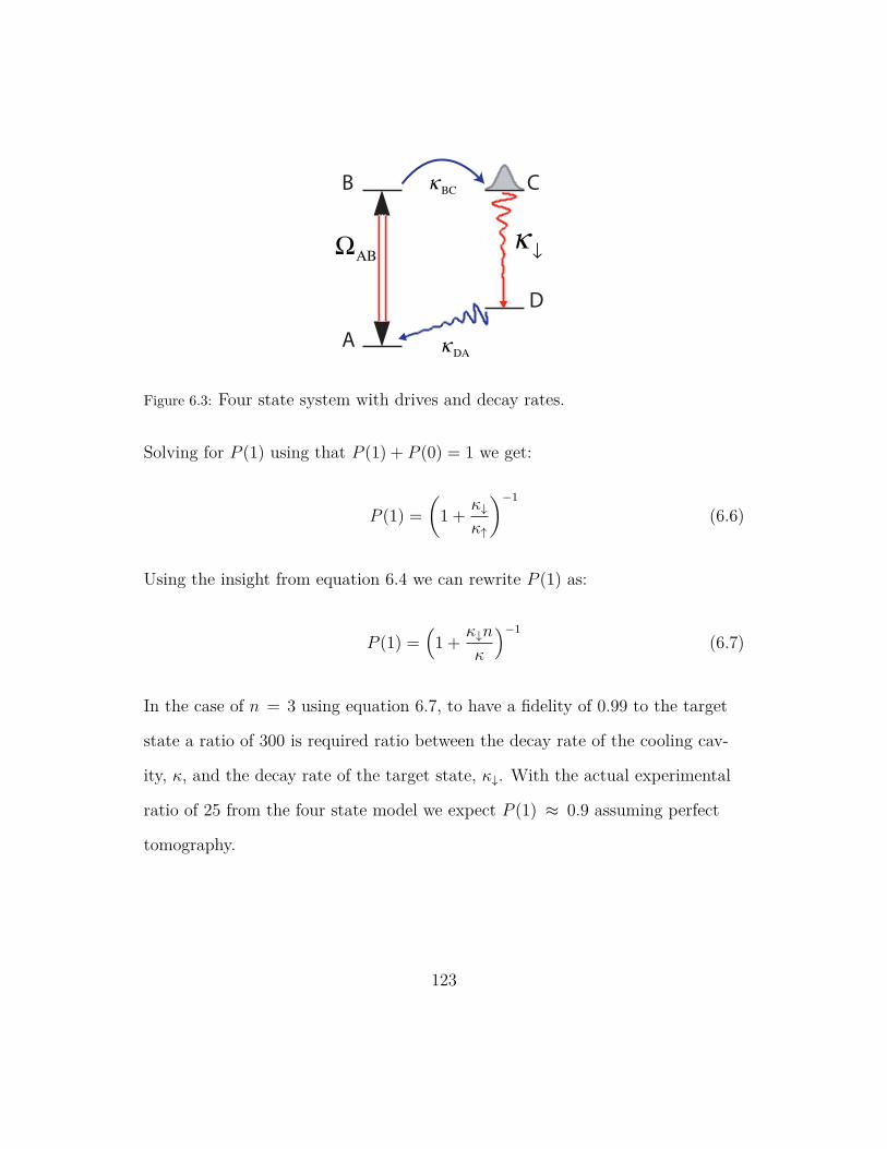
A
C
D
B
! !
! DA
!AB
! BC
Figure 6.3: Four state system with drives and decay rates.
Solving for P (1) using that P (1) + P (0) = 1 we get:
P (1) =
(1 +
κ↓
κ↑
)−1
(6.6)
Using the insight from equation 6.4 we can rewrite P (1) as:
P (1) =(1 +
κ↓n
κ
)−1
(6.7)
In the case of n = 3 using equation 6.7, to have a fidelity of 0.99 to the target
state a ratio of 300 is required ratio between the decay rate of the cooling cav-
ity, κ, and the decay rate of the target state, κ↓. With the actual experimental
ratio of 25 from the four state model we expect P (1) ≈ 0.9 assuming perfect
tomography.
123

6.3 Linblad Master Equation and Simulation
To improve upon the four state model we will run a simulation of the Linblad
equation for our driven, dissipative system. Our Hamiltonian including only
cavity terms is:
H/ℏ = ωsb†b+ ωcc
†c− As
2b†2b2 − Ac
2c†2c2 − χscb
†bc†c (6.8)
In terms of these Hamiltonian parameters the FSSP will work best for χsc >
κc ≫ κs and As ≫ κs. To incorporate continuous wave drives into our Hamilto-
nian we begin by adding stiff drives of the form ΩS(b†+b) for the storage cavity
drive and ΩC(c† + c) for the cooling cavity drive. Where ΩS and ΩC are complex
drive amplitudes. By including these drives and entering the rotating frame of
both cavities Us = exp(ib†bωdst) and Us = exp(ic†cωdct) we result in detunings
of ∆s = ωs − ωds for the storage cavity and ∆c = ωc − ωdc for the cooling cavity.
We note that ωds and ωdc are the frequencies of the drives on the storage and
cooling cavity respectively. Our driven Hamiltonian is now:
H/ℏ = ∆sb†b+∆cc
†c− As
2b†2b2 − Ac
2c†2c2
−χscb†bc†c+ ΩS(b
† + b) + ΩC(c† + c) (6.9)
With this driven Hamiltonian we can write the master equation for our system
as:
ρ = −i[H, ρ] + κsD[b]ρ+ κcD[c]ρ (6.10)
124
The above master equation is used in QuTIP 2.2 [101] with the steady state
solver and the time dependent solver to produce the simulation results that ap-
pear in Fig. 6.12(b),(c),(d) and Fig. 6.11(b),(c). The code used for the simula-
tions is found in appendix B. From simulation we find the stabilization rate to
be κ↑ ≈ κ/9.
6.4 Photon Number Calibration via the AC stark effect
In this section we develop a method for determining the average photon number
in a fast cavity. Fast cavities, relative to the quantum object they are measur-
ing, are crucial for repeated quantum measurements [106, 108]. The goal in this
procedure is to use the AC stark effect on the qubit as a method of determin-
ing the average photon number in a fast cavity given some room temperature
drive strength or in the actual experimental setup the drive power. If the drive
is place at ωd = (ωgc + ωe
c)/2 then our measurement efficiency which is the aver-
age I quadrature measured value, Im , divided by its standard deviation, σ, is:
Imσ
=1
Tm
∫ Tm
0
√ηκTm|αg(t)− αe(t)|2dt ≈
√2ηκTmn sin
(θ
2
)(6.11)
Where Tm is the measurement time , η is the quantum efficiency, κ is the de-
cay rate of our fast cavity, and αe,g(t) is the amplitude of our cavity displace-
ment for either the excited or ground state of the qubit. This integral can be
approximately evaluated to give the right hand side which has the average pho-
ton number in the fast cavity n as well as the sine of half the angular separation
between the two coherent states. Since the actual measurement will be average
125

Figure 6.4: AC Stark Photon Number Calibration. (Top) Different points on thequbit Bloch sphere are shown. For an arbitrary superposition of these valueswe can measure the projection along the I and Q quadratures. We will say thateach ’g’ or ’e’ distribution has an associated cavity displacement of αg, αe . Wewill say that the full angular separation between the two distributions is θ andthat each distribution has a width of 2σ.
126

photon number we square the above result to get:
(Im2
)2
≈ 2ηκTmn sin2
(θ
2
)≡ Γϕ (6.12)
In equation 6.12 we define this quantity as our dephasing rate. We can now
use equation 6.12 to express the amplitude of our AC stark measurement, where
T is the time between our qubit rotations, as:
A = exp (ΓϕT )
A = exp
(−2ηκTmn sin2
(θ
2
)T
)A = = exp (ΓT ) exp
(−2κTmn sin2
(θ
2
))(6.13)
Since we will be operating in the regime that χ ≈ κ we can take the simplifi-
cation of:
sin2
(θ
2
)≈ χ2
χ2 + κ2(6.14)
We recognize that the amplitude of our response is written in the form of
Ae−Bn. We further make the observation that the average photon number in
the cavity will be proportional to the drive power we use, Pd. So we analogously
expect that the amplitude of our response in terms of the drive power, Pd, will
be of the form De−CPd . By relating the arguments of the exponentials the aver-
age photon number in the cavity can be related to the room temperature drive
power as:
n =
(2κTm
χ2
χ2 + κ2
)−1
CPd (6.15)
127

From this expression the only unknown is the constant, C. This constant,
along with other measurement parameters, converts room temperature drive
power to the average photon number in the cavity. It is quite remarkable that
one constant can take into account all the attenuation, intended or otherwise,
as well as reflections in the lines. To determine this constant, we perform the
procedure in Fig. 6.5a. The first step is a π2 qubit rotation around the x axis,
a drive on the cavity at ωd that is long enough so that steady state is reached
in the cavity, a wait time which is five times the cavity decay time allowing the
cavity to be fully evacuated, and finally a second π2 qubit rotation at various an-
gles around the x axis creating oscillations in the measured signal. We fit the
measured oscillation to a sine wave to extract the amplitude (6.5b ). By repeat-
ing this protocol several times for different drive powers applied to the cavity,
the decay of the amplitude versus the cavity drive power (6.6) can be plotted.
By plotting the amplitude of the response versus the amplitude power an ex-
ponential can be fit to the data so that the constant, C, can be extracted. By
driving at ωd = (ωgc + ωe
c)/2 all of the dephasing information is in the ampli-
tude and not the phase of the oscillation. In our particular setup we found that
roughly .24 mW of room temperature drive power was required per average pho-
ton in the cooling cavity.
128

300
250
200
150Rea
dout
Sig
nal (
µV)
0
Rotation Angle (radians)
3!2
5!2
7!2
9!2
11!2
a
b
R x (!2 )
500 ns2µs
MeasurementR x (! )Cavity Drive
Figure 6.5: Representative data from performing the measurement in Fig. 6.6a.In red circles are the result of a measurement with a weak drive strength and inred diamonds are the result of a measurement with larger drive strength. Theamplitude for these as well as others are plotted as a function of room tempera-ture drive power in Fig. 6.6b.
6.5 Hamiltonian Parameters
From the previous sections we gained the insight that the requirements for the
FSSP are: that the ratio of lifetimes between the cooling cavity and storage cav-
ity must be large, that the storage cavity must be anharmonic enough such that
129

70605040302010
0Ram
sey
Ampl
itude
(uV)
10-7 10-6 10-5 10-4
Power (Watts)
Figure 6.6: AC Stark calibration. (a) A rotation of π/2 is performed around thex axis of the qubit’s Bloch sphere. A cavity drive at (ωg
c + ωec)/2 is applied for
a duration of two microseconds allowing the cavity to reach steady state. Thedrive is then turned off, the cavity fully evacuates and a final π/2 is performedat various angles with respect to the x axis. This allows for oscillations of thequbit state between ‘g’ and ‘e’. (b) The amplitude of oscillation is then plottedas a function of drive power. From this an exponential can be fit and the decayof that exponential is used to calibrate the average photon number in the fastreadout cavity.
130
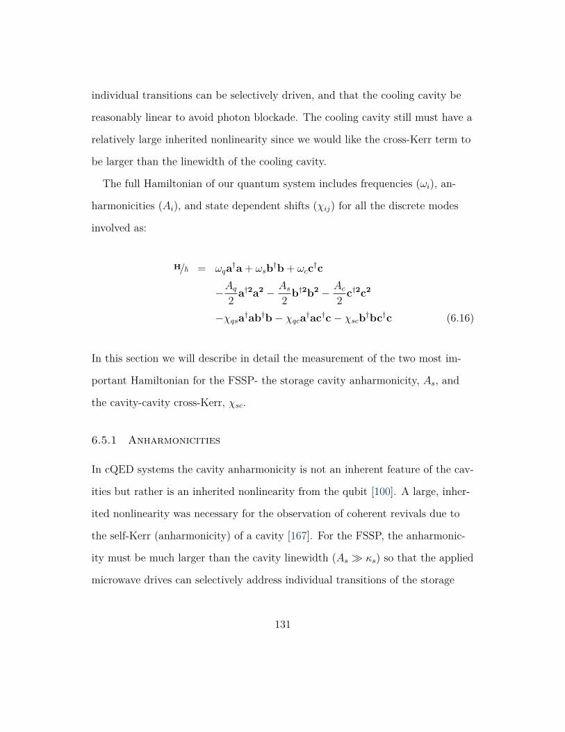
individual transitions can be selectively driven, and that the cooling cavity be
reasonably linear to avoid photon blockade. The cooling cavity still must have a
relatively large inherited nonlinearity since we would like the cross-Kerr term to
be larger than the linewidth of the cooling cavity.
The full Hamiltonian of our quantum system includes frequencies (ωi), an-
harmonicities (Ai), and state dependent shifts (χij) for all the discrete modes
involved as:
H/ℏ = ωqa†a+ ωsb
†b+ ωcc†c
−Aq
2a†2a2 − As
2b†2b2 − Ac
2c†2c2
−χqsa†ab†b− χqca
†ac†c− χscb†bc†c (6.16)
In this section we will describe in detail the measurement of the two most im-
portant Hamiltonian for the FSSP- the storage cavity anharmonicity, As, and
the cavity-cavity cross-Kerr, χsc.
6.5.1 Anharmonicities
In cQED systems the cavity anharmonicity is not an inherent feature of the cav-
ities but rather is an inherited nonlinearity from the qubit [100]. A large, inher-
ited nonlinearity was necessary for the observation of coherent revivals due to
the self-Kerr (anharmonicity) of a cavity [167]. For the FSSP, the anharmonic-
ity must be much larger than the cavity linewidth (As ≫ κs) so that the applied
microwave drives can selectively address individual transitions of the storage
131
400380360340320300280
8.5008.4958.4908.4858.480
Data Model
fs,0→1fs,1→2
Read
out (
µV)
Frequency (GHz)
fs,0→2
2
Figure 6.7: Storage cavity spectra. Spectroscopy is performed on the storage cav-ity with a single CW drive. With a large amplitude drive, we observe the twophoton transition, fs,0→2
2. From this measurement we infer the location of the
fs,1→2 transition (black line) and determine its detuning from the fs,0→1 tran-sition as 4.0 MHz which we define as the anharmonicity of the storage cavity.
cavity. Large or measurable anharmonicities are not universally desirable. For
instance, in the case of cat states an anharmonicity is a method of decoherence
ruining the quantum state. Efforts in correcting evolution due to inherited cav-
ity anharmonicity show promise [53, 51, 50].
To measure the storage cavity anharmonicity, we use a single CW drive to
perform spectroscopy (Fig. 6.7) which was performed using a dispersive mea-
surement with the measurement tone applied at the cooling cavity low power
peak. Explicitly this means that when the spectroscopy tone is applied to a
frequency that has a negligible contribution to a resonance we get full trans-
mission through the cooling cavity and when the spectroscopic tone excites the
mode under investigation it shifts the resonance frequency of the measurement
tone reducing the transmission through the cooling cavity. Using a large ampli-
tude drive on the storage cavity which power broadens the fs,0→1 fi = (ωi/2π)
132

6
4
2
0
9.3209.3169.312Re
adou
t (µV
)Frequency (GHz)
fc1
fc2
fc3 fc
0
Data Fit
χsc
Figure 6.8: Cooling cavity spectra. A 5 ns displacement pulse, whose amplitudegives n ≈ 1.5 in the storage cavity, enables the observation of a single photonresolved cross-Kerr between the two cavities, χsc(2π)
−1 = 2.59± .06 MHz.
transition, we observe the two photon transition with frequency fs,0→2
2. The de-
tuning corresponds to half the anharmonicity, Ai =Ai/2π, of the storage cav-
ity and we infer an inherited cavity anharmonicity As = 4.0 MHz. Following
the same method, we determine that the cooling cavity anharmonicity to be
Ac = 300 kHz and the qubit anharmonicity to be Aq = 26.1 MHz. The cooling
cavity anharmonicity was measured in this fashion when it was weakly coupled
to the 50 ω environment. During the FSSP when its linewidth was large (1.7
MHz) we verified this anharmonicity by knowing the drive power correspond-
ing to one photon in the cooling cavity and by varying the drive power we could
extract the anharmonicity from the frequency shift of the cooling cavity.
6.5.2 Cavity-Cavity Cross-Kerr
In this section measurements of the state dependent shift between the storage,
cooling, qubit modes are undertaken. The state dependent shift between two
coupled cavities was predicted to be be measurable [168] and this state depen-
133

dent shift is the unique measurement in this section. Excitations for each mode
is performed sequentially, rather than concurrently since off resonant drives re-
sult in larger than actual state dependent shifts [169]. To measure the state
dependent shift between the two cavities we first perform a 5 ns square pulse
which displaces the state of the storage cavity, then a 2 µs square pulse on the
cooling cavity, and finally high-power readout on the cooling cavity which relies
on the anharmonicity of the cooling cavity for signal [115]. Shown in Fig. 6.8 is
a spectroscopy measurement of the cooling cavity for a displacement n ≈ 1.5
of the storage cavity. Discrete spectral peaks for up to three photons in the
storage cavity are visible. From this we infer a state dependent shift χsc/2π =
2.59± .06 MHz and observe the first single photon resolved cavity-cavity cross-
Kerr.
A similar method is used to measure the state dependent shift, χqs between
the qubit and the storage cavity. We apply a 5ns square pulse which displaces
the state of the storage cavity, a 2 µs square pulse on the qubit, and perform
high-power readout on the cooling cavity which relies on the anharmonicity of
the transmon for a readout signal. To measure the state dependent shift, χqc
between the qubit and the cooling cavity we use a slightly different approach
because of the weak readout signal 6.8. Instead we perform a π/2 on the qubit,
then a 2 µs square pulse on the cooling cavity, and finally high power read-
out on the cooling cavity. In summary we find our Hamiltonian parameters
(χij =χij/2π, Ai = Ai/2π) to be:
134

Term Measured Value Simulation Prediction Units
fq 7249.46± .01 7221 MHz
fs 8493.73± .02 8564 MHz
fc 9320.11± .02 9346 MHz
Aq 26.1± .3 25.9 MHz
As 4.0± .1 3.7 MHz
Ac 300± 80 240 kHz
χqs 21.1± .1 19.8 MHz
χqc 4.9± .1 4.2 MHz
χsc 2.59± .06 2.2 MHz
κs 65± 5 — kHz
κc 1.7± .1 — MHz
Table 6.1: FSSP Hamiltonian parameters as well as the predicted parametersfrom a BBQ simulation. The predicted values are quite close to the measuredvalues and the major sources of error are machining tolerances, and placementof the vertical transmon.
6.6 Photon Number Selective π Pulse Calibration
From table 6.1 we see that the necessary relations for the FSSP are satisfied
(χsc > κc ≫ κs and As ≫ κs). However, we must develop the tools nec-
essary for cavity state tomography to measure the target state of the FSSP.
First we require photon number selective π pulses on the different resonance
frequencies of the qubit which are dependent on the number of excitations in
135

the storage cavity (f nq ≈ f 0
q − nχqs). To do calibrate these π pulses multiple
cavity displacements are performed allowing the measurement of Rabi oscilla-
tions for each of the different photon number peaks of the qubit. Due to the
large state dependent shift between peaks (21 MHz), each qubit transition will
require a different drive amplitude for a full π pulse. We find that each subse-
quent transition requires roughly 10% larger amplitude than the previous tran-
sition. Once the π pulses for each photon number peak are calibrated a good
check is to perform cavity displacements on the storage cavity and measure the
photon number distribution (Fig. 6.9). For each displacement, the photon num-
ber distribution will be Poissonian. From this set of measurements we have a
collection of background subtracted raw data that in Fig. 6.9 is plotted versus
AWG DAC amplitude for the 5 ns displacement pulse. With these five traces
we perform a global fit on the traces which gives not only the y scaling, photon
number probability, but also x scaling, root photon number. We can see from
Fig. 6.9 that for larger cavity displacements (n ≳ 2) will have appreciable un-
certainty in our results. However, for smaller average photon numbers (n ≲ 2)
in the storage cavity we can reliably measure the photon number distribution.
We attribute difficulties in measuring larger photon number distributions to the
large cross-Kerr saturating the readout mechanism.
136

6.6.1 π Pulse Selectivity
To estimate the selectivity, S, of our π we use the following [137]:
S =(1 +
π
8exp
(−(χqs/σw)
2))−1
(6.17)
Here we assume a gaussian pulse with spectral width σw and with peak spacing
χqs. In our particular case, χqs is the state dependent shift between the qubit
and the storage cavity but in general this is just the spacing between the dif-
ferent photon number peaks. From eq. 6.17 the estimated selectivity of our π
pulses (χqs = 21.1 MHz and σw = 4 MHz) for the different photon number
peaks is no worse than .999. We experimentally investigate the contribution to
π pulse selectivity by applying a gaussian π pulse on the N = 0 and measuring
the population in the N = 1 photon peak and find that our induced transition is
no worse than .3%, a bound limited by averaging.
6.7 Fock State Stabilization Protocol
Shown in Fig. 6.2(b) is the QRE protocol we will use to stabilize Fock states in
the storage cavity. This protocol is conceptually similar to the protocol used in
Ref. [99] which stabilized the ground state of a qubit tensor product with a co-
herent state of a cavity. The FSSP in some sense generalizes DDROP allowing
the physicist to not only stabilize the vacuum state but also any exact excita-
tion number. In this section we will present results stabilizing not only the zero
photon Fock state of the storage cavity but also the first Fock state of the stor-
137

16
12
8
4
0
Rea
dout
(mV)
80006000400020000Amplitude (DAC)
N0 N1 N2 N3 N4
Figure 6.9: Photon number selective π pulse response versus room temperaturedisplacement amplitude. Measurement of the different photon number peaks ofthe qubit as a function of displacement amplitude. Photon number peaks of thetransmon qubit due to the storage cavity are measured up to N=4. This is datais background subtracted and plotted as a function of AWG DAC value for theamplitude of the 5 ns displacement pulse. From this a global fit is performed onthe entire set of measurements determining the x scaling, root photon number,and y scaling, probability. We attribute the difficulty in measuring higher pho-ton numbers to the saturation of our readout mechanism due to the large directcross-Kerr readout.
138
age cavity.
To implement the FSSP the frequencies of the two microwave drives and their
amplitudes must be chosen judiciously. For the drive applied to the storage
cavity we find optimum performance both experimentally and simulation for a
drive strength ΩS ≈ κc. In figure 6.10 the storage cavity drive is placed at fs,0→1
with drive strength ΩS ≈ κc. Since the cooling cavity is weakly anharmonic we
expect that its frequency will change dependent on its average photon number.
In figure 6.10 (a) is the pulse scheme used to implement the FSSP. Contin-
uous wave drives are applied to the storage cavity and the cooling cavity for a
duration that is two hundred times longer than κc which is the rate at which
steady state will be reached. Furthermore, this pulse duration is roughly ten
times longer than the decay time of the storage cavity meaning that any steady
state achieved through the FSSP has overcome the internal decays of either cav-
ities. Next a wait time of 300ns wait time follows the long CW pulses so that
fast photons can leak out of the cooling cavity. Finally photon number selective
π pulses (σt = 40 ns) are applied to measure the photon number probability
distribution. In figure 6.10(b,c) the frequency of the storage drive is held fixed
at the fs,0→1 transition with a drive strength roughly equal to κc. The parame-
ters swept in figure 6.10 are the drive strength of the cooling drive, which alters
the size of the coherent state the cooling cavity is conditionally displaced to,
as well as the drive frequency of the cooling cavity which determines whether
the zero or one photon Fock state of the storage cavity is stabilized. The drive
strength applied to the cooling cavity is calibrated via the AC Stark dephasing
139

method described in section 6.4. The drive frequency is plotted as a detuning,
∆ = ω0c − ωdc, and normalized by the cross-Kerr, χsc. The drive frequency on
the cooling cavity is normalized by the cross-Kerr to illustrate that at about
one cross-Kerr, with a sufficiently strong drive, a one photon Fock state is sta-
bilized. Since the cooling cavity is weakly anharmonic maximum stabilization of
the first Fock state of the storage cavity will not happen for ∆ = χsc but will
happen at a lower frequency and therefore a larger detuning. From simulation,
we expect on average four photons will be in the cooling cavity for maximum
stabilization of the first Fock state of the storage cavity. Four photons in the
cooling cavity with an anharmonicity of 300 kHz corresponds to the extra half
cross-Kerr observed in figure 6.10. This explains why maximum stabilization for
the first Fock state occurs for ∆ ≈ 1.5χsc. From the linecuts in figure 6.10 we
see that for a sufficiently strong drive strength on the cooling cavity that we can
either stabilize a zero or one photon Fock state of the storage cavity solely as a
function on the placement of the cooling cavity drive. We define the probability
of getting exactly N photons in the storage cavity as P (N). We measure proba-
bilities for N = 0 to N = 3. At the optimum parameter selection for the cooling
cavity drive we stabilize vacuum of the storage cavity with P (0) = 0.96 ± 0.03
and stabilize the one photon Fock state with P (1) = 0.63± 0.02.
6.7.1 Comparison DDROP and FSSP
In table 6.2 a direct comparison is made between the results of DDROP and the
FSSP when stabilizing the ground state of a qubit or in the case for the FSSP
140

b
c
1.00.80.60.40.20.0
Prob
abilit
y
-10
-5
0
5
P driv
e (d
B)
1.0
0.5
0.0Prob
abilit
y
3210-1Drive frequency ( sc)
-1.5dB -8.5dB
-10
-5
0
5
P driv
e (d
B)
1.0
0.5
0.0Prob
abilit
y3210-1
Drive frequency ( sc)
a Stabilization drives ON
300 nsStabilization time (Ts)
detect N in storage
MeasurementR x,!N
-1.5dB -8.5dB
N=0 N=1
Figure 6.10: Photon number probabilities of the zero and one photon Fockstates from the FSSP. (a) The Fock state stabilization protocol described inFig. 6.2(b) is applied for a duration, Ts, followed by a 300 ns wait to evacuateexcitations from the cooling cavity, a photon selective π pulse is then performedon the qubit determining the probability of each photon state of the storagecavity up to three photons. (b) Storage cavity photon number probability (N=0left and N=1 right) as a function of drive amplitude and frequency. The fre-quency of the cooling cavity drive is plotted as ∆ = ω0
c − ωdc, and normalized bythe cross-Kerr, χsc. As the frequency of the drive applied to the cooling cavity isbrought in resonance with the first photon peak of the storage cavity ∆/χsc ≈ 1the protocol stabilizes the first Fock state of the storage cavity. The inset is asimulation plot with the same axis and color scale as the experimental result.(c) Linecuts (dashed lines in part b) for a weak drive power and a drive powerresulting in stabilization.
141

DDROP FSSP
Vacuum Stabilization 0.993± 0.005 0.96± 0.03
κc/κ(q,s) ≈ 700 25A(q,s)/Ac ≈ 3000 15χ(q,s)c/κc ≈ 2.3 1.5
Table 6.2: FSSP Hamiltonian parameters as well as the predicted parametersfrom a BBQ simulation. The predicted values are quite close to the measuredvalues and the major sources of error are machining tolerances, and placementof the vertical transmon.
a microwave cavity. Although the FSSP did not outperform DDROP it is not
a truly ‘apples’ to ‘apples’ comparison which is shown in the remaining lines in
table 6.2. The predominant reason for DDROP out performing the FSSP is due
to the larger ratio of lifetimes in the DDROP experiment. Other parameters,
such as the linearity of the cooling cavity as well as the separation of photon
number peaks matter weakly in this comparison. Although for if higher photon
numbers were stabilized these parameters would matter more.
6.7.2 Steady State Wigner Function for Stabilized N=1 Fock State
To demonstrate the oscillator nature of the storage cavity in Fig. 6.11 (a) we
perform cavity tomography after the FSSP measuring generalized Husimi Q
functions [167] defined as:
QN(α) =1
π| ⟨N |D−α |Ψ⟩ |2 (6.18)
142

D−α is the displacement operator, and |Ψ⟩ is the final state. In our case |Ψ⟩
will be the steady state to the FSSP. Although the zeroth Husimi Q function
entirely describes the state of the oscillator we measure generalized Husimi Q
functions up to N = 3 Fock state of the storage cavity so that we can infer
the Wigner function. By adding and subtracting the even and odd measured Q
functions the Wigner function is:
W (α) =2
π
∞∑n=0
(−1)nQn(α) (6.19)
The Wigner function is measured in this manner because of the large state de-
pendent shift, χqs, between the qubit and the storage cavity. The preferred
method to measure a Wigner function directly measures photon number par-
ity. To measure photon number parity requires π pulses which are not photon
number selective. For instance, a π pulse with σt = 5ns gives a spectral width
of roughly 32 MHz which for a qubit-cavity state dependent shift of 21 MHz is
insufficient. In cases with large state dependent shifts, it is necessary to measure
the generalized Husimi Q functions. Since it is not practical to measure all the
Husimi Q functions a truncation must be made. This truncation could result in
a halo effect in the Wigner function. Although a small effect, one can see that
in figure 6.11 (b) that on the corners of the Wigner function the measurements
are skewed towards negativity (red). Furthermore, by constructing the Wigner
function through a series of generalized Husimi Q measurements rules out the
possibility of QND measurements of photon number parity. By comparing the
measured Wigner function to a simulation of the steady state solution to the
143

FSSP when stabilizing a one photon Fock state we are confident that the neg-
ativity at the origin in our Wigner function is a real result and not due to the
slight bias in our measurement. As can be seen in figure 6.11(b,c) the harmonic
oscillator picture describes the steady state of the storage cavity as a statistical
mixture of P (0) = 0.37 ± 0.03 and P (1) = 0.63 ± 0.02 with no statistically
significant population in the N = 2, 3 states. In Fig. 6.11 c statistically signif-
icant negativity in the Wigner function is observed. With harmonic oscillators
Wigner functions are often shown since negativity in the Wigner function indi-
cates a quantum state. What is quite special here is that we observe negativity
in the Wigner function for arbitrarily long stabilization times. In this case the
stabilization protocol was run for ten times the storage cavity lifetime. Without
the FSSP the storage cavity would have fully decayed in that amount of time.
6.7.3 Interpreting Results as a Spin System
Since the results of the FSSP have the storage cavity limited to its first two
Fock states, we can recast our results in a way analogous to a spin system. The
figure of merit will be the polarization, p defined by p = P (0)−P (1)P (0)+P (1)
. In a spin
system with many spins in thermal equilibrium with their bath and there ex-
ists and external magnetic field, B, than it makes sense to discuss the net po-
larization of the spin ensemble. At zero Kelvin we expect the spin system to
overwhelmingly be aligned with the external magnetic field since the bath can-
not provide the energy necessary to align against the magnetic field. However,
as the temperature of the bath is increased thermal fluctuations provide indi-
144

b
c
a Stabilization drives ON
300 nsStabilization time (Ts)
Wigner Tomography
MeasurementR x,!N
αα
α
α αPa
rity
Parit
y
0.0
0.3
-0.3
D!!†
Figure 6.11: Wigner tomography of stabilized steady state of the storage cavity.(a) The previously described stabilization protocol is used to reach the desiredsteady state. Then Wigner tomography is performed on the state of the storagecavity. (b) Left: Measured Wigner function for the steady state of the storagecavity which is a statistical mixture of an N = 1 and N = 0 Fock state. Right:Simulated steady state of the protocol. (c) Linecuts along Im(α) and Re(α) forthe measured Wigner function and the simulated steady state Wigner function.Although not a pure N = 1 Fock state of the storage cavity our long term solu-tion does have negativity in the Wigner function indicative of a quantum state.
145

vidual spins with the necessary energy to align against the magnetic field. As
infinite temperature is approached, the spin ensemble will not have a net polar-
ization since as a whole the spin ensemble will have as many spins aligned with
the magnetic field as those that are anti-aligned. In the case of a discrete, quan-
tum system, by continuing to add energy to the bath paradoxically the spin sys-
tem will become predominately anti-aligned to the magnetic field making this
system more ordered and decreasing its entropy. This process is how a polariza-
tion inversion can be created. For the net spin system to be fully anti-aligned
to the external magnetic field a tremendous amount of energy must be available
from the environment. Oddly enough, we see that as we increase the available
energy in the bath the spin system becomes more ordered. The entropy of the
spin system has decreased. With this in mind we may now define temperature
in terms of the polarization as [170]:
T =hfs,0→1
2kB tanh−1 (p)(6.20)
Where h is Planck’s constant and kB is Boltzmann’s constant. From this we
infer that our steady state solution corresponds to an effective negative temper-
ature of −0.77± 0.06 K in equilibrium with the storage cavity.
We plot the steady state polarization, p, of the storage cavity after running
the FSSP in Fig. 6.12(b). When ΩC is driven at the zero photon peak of the
cooling cavity we observe p = 0.95 ± .04 demonstrating that storage cavity is
overwhelming in the zero photon Fock state despite the induced Rabi drive on
the storage cavity. However, as the drive power and frequency applied to the
146

cooling cavity are varied, steady state stabilization of a polarization inversion
occurs corresponding to a predominantly one photon Fock state in the storage
cavity. The ability to realize a population inversion is a purely quantum effect.
In Fig. 6.12(d) we see the time dynamics of this protocol where the initial
polarization is unity then changing as a function of time to its steady state
value of p = −0.26 ± 0.04. Plotted on top of the data is a full simulation of
our driven dissipative system where we find excellent agreement in our time
dynamics [101]. From the four state model, we would expect a polarization of
p = −0.47. This value is within a factor of two of both what is measured experi-
mentally and extracted from a full simulation of the Linblad equation. Through
simulation of the full Linblad master equation we find that the limitation in po-
larization inversion is the finite ratio of lifetimes. Physically realized two cav-
ity systems exist with a ratio of lifetimes being a factor of one thousand [108].
With that ratio we expect that in steady state P (1) > 0.99.
6.8 Future Improvements
The major limitation of this implementation of the FSSP was our modest ra-
tio of lifetimes between the storage cavity and the cooling cavity, κc/κs ≈ 25.
This ratio is most likely set by the Purcell effect between the two cavities. To
mitigate the Purcell effect between the cavities, we could improve the design
of the qubit and increasing its anharmonicity. In this sample the transmon an-
harmonicity was 26 MHz. This small anharmonicity is in part a consequence of
the geometrical capacitance overwhelming the qubit design which has a total
147

b
c
a Stabilization drives ON
300 nsStabilization time (Ts)
detect N in storage
-10
-5
0
5
P driv
e (d
B) 0.0
1.0
-1.0
-1.0
0.0
1.0
Pola
rizat
ion -1.5 dB
-8.5 dB
Pola
rizat
ion
Pola
rizat
ion
3210-1Normalized detuning ( sc)
d
Stabilization time (µs)
region of T<0
-1.0
0.01.0
20016012080401.00.50.0
MeasurementR x,!N
Figure 6.12: Storage cavity polarization. (a) The Fock state stabilization protocoldescribed in Fig. 6.2(b) is applied for a duration, Ts, followed by a 300 ns waitto evacuate excitations from the cooling cavity, a photon selective π pulse isthen performed on the qubit determining the probability of each photon state ofthe storage cavity up to three photons. (b) Storage cavity state polarization asa function of drive amplitude and frequency. The frequency of the cooling cav-ity drive is plotted as ∆ = ω0
c − ωdc, and normalized by the cross-Kerr, χsc. Asthe frequency of the drive applied to the cooling cavity is brought in resonancewith the first photon peak of the storage cavity ∆/χsc ≈ 1 the protocol stabilizesthe first Fock state of the storage cavity. The inset is a simulation plot with thesame axis and color scale as the experimental result. (c) Linecuts for a weakdrive power and a drive power resulting in a polarization inversion. (d) As theduration of the stabilization protocol is varied the polarization of the storagecavity alters and for infinite time reaches its steady state solution.
148
length of 5mm. In addition, the strong coupling between the transmon and the
storage cavity has the storage cavity inherit a large fraction of the transmon’s
nonlinearity. To improve the transmon’s anharmonicity a gap capacitor could
be implemented on one or both sides of the junction to decrease its geometrical
capacitance. To get a sense for how an increased transmon anharmonicity would
help the FSSP results we look at a simple Purcell calculation which gives:
κS ≈ g 2S∆2
S
g 2C
∆2CκC ≈ χSC
2αqκC (6.21)
For this simple estimation we would expected a ratio of lifetimes to be of or-
der 20 and in experiment we see a ratio of 25. However, if our transmon an-
harmonicity were increased by a factor of ten then we would expect a simple
Purcell limitation resulting in a ratio of lifetimes between the storage and cool-
ing cavity in excess of 250. From this we would expect to stabilize a one pho-
ton Fock state with P (1) > .87 and a polarization of p < −.74. To further
improve the ratio of lifetimes between the storage cavity and cooling cavity a
Purcell filter such as the waveguide Purcell filters made in Qlab is necessary.
An outstanding issue in superconducting circuits is coupling long lived elements
such as cavities to less coherent elements such as qubits or readout cavities. For
successful integration, without comprising coherence, work must continue in de-
veloping novel approaches to merge highly coherent devices with intentionally
short lived quantum objects.
149
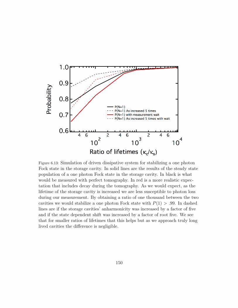
Figure 6.13: Simulation of driven dissipative system for stabilizing a one photonFock state in the storage cavity. In solid lines are the results of the steady statepopulation of a one photon Fock state in the storage cavity. In black is whatwould be measured with perfect tomography. In red is a more realistic expec-tation that includes decay during the tomography. As we would expect, as thelifetime of the storage cavity is increased we are less susceptible to photon lossduring our measurement. By obtaining a ratio of one thousand between the twocavities we would stabilize a one photon Fock state with P (1) > .99. In dashedlines are if the storage cavities’ anharmonicity was increased by a factor of fiveand if the state dependent shift was increased by a factor of root five. We seethat for smaller ratios of lifetimes that this helps but as we approach truly longlived cavities the difference is negligible.
150

6.8.1 Final Comment
In this chapter the first single photon cavity-cavity cross-Kerr is presented. This
large cavity-cavity state dependent shift was developed so that we could imple-
ment the FSSP. Future applications of the cross-Kerr are in a QRE scheme that
stabilizes an even two ‘cat’ state of a cavity [158], as well as, serving as a direct
cavity-cavity entangling operation. A one photon Fock state, as well as, the vac-
uum state of the storage cavity were stabilized. To achieve this stabilization, we
demonstrated a considerable level of mastery and conceptual understanding was
required over a driven, dissipative cavity centric protocol adding to the general
knowledge base of the cQED community. Going forward it is unclear what role
QRE will play in the pursuit of a quantum computer. It may be the case that
QRE protocols are most useful in stabilizing either a logical state, or a subset
of logical states. The advantage of QRE is that the feedback loop is built into
the Hamiltonian whose latency is most likely less than protocols that require
measurements of ancillary systems with external feedback.
151

7Conclusion & Outlook
7.1 Conclusion
In the past six years the amount of progress and growth of the superconducting
community has been to say the least impressive. Year over year improvements
in quantum device coherence times (Fig. 7.1) coupled with an increasing num-
ber of experimental and theoretical groups bringing a diversity of ideas to the
152

field position the quantum circuit community for continued success. Indicative
of this growth is a long standing memory I will have from the 2014 APS March
Meeting in Denver, CO where fire regulations prevented many physicists from
attending talks and one person in particular was only able to enter for her pre-
sentation through polite and persistent discourse [74]. This thesis is part of the
progress in the last six years. Some parts will pay large dividends in the future
as quantum systems increase in size and complexity as 3D integration becomes
necessary. Other parts are reflective of great advances in classical and quantum
simulation capabilities. The ability to predict purely quantum effects through
classical electromagnetic simulation is an under appreciated development. Fur-
thermore, the ubiquity of open source quantum simulation capabilities such as
QuTIP enable deeper synthesis between theory and experiment.
7.2 Future Experiments
In this section future work will be discussed based on accomplishments from
previous chapters. This list is not exhaustive nor does it include applications for
existing theoretical proposals. For instance, Ref. [158] relies on a large cavity-
cavity state dependent shift, along with parametric processes, to stabilize the
even two component Schrödinger cat state of a cavity.
7.2.1 Extension to Fock State Stabilization
The first possible experiment is applying the Fock state stabilization protocol
discussed in chapter 6 to stabilize higher Fock states of a microwave cavity. The
153

setup would be very similar to chapter 6 where a storage cavity is strongly cou-
pled to a cooling cavity. The decay rate of the cooling cavity must be fast com-
pared to the storage cavity. To alter the protocol in chapter 6, it would require
adding Rabi drives between adjacent Fock states of the storage cavity up to the
desired Fock state for stabilization. In a sense this can be thought of creating a
“Rabi ladder” between vacuum and the desired Fock state to be stabilized. The
final drive needed would be applied at the cooling cavity but detuned by the
number of cross-Kerrs (ωNC = ω0
C − NχSC) corresponding to the N such Fock
state to be stabilized.
On an experimental front, realizing a highly coherent cavity strongly cou-
pled (enough to inherit ∼ 1 MHz of anharmonicity) to a transmon stands as a
formidable challenge. Ideally, one would use a cavity with coherence times of or-
der 1 ms so that a variety of Fock states could be stabilized with high fidelity.
Accomplishing this is nontrivial and requires a fair amount of development.
However, the payoff could be realized in the next section.
7.2.2 N00N State Stabilization
References [155] and [156] both leveraged quantum reservoir engineering pro-
tocols to stabilize a Bell state of two qubits. One could recast these results as
the stabilization of a N00N state where e → N = 1, and g → N = 0. With
this observation there are two possible options to stabilize N00N states with
N > 1. One possibility would be to have two weakly anharmonic transmons
coupled to a cooling cavity. The other possibility uses two storage cavities that
154
are strongly coupled to transmons to inherit nonlinearity as well as a cooling
cavity which acts as an entropy dump. The second approach has the advantage
of one being able to claim that the cavities have no innate nonlinearity at the
expense of requiring more ‘hardware’.
For the remainder of the discussion we will gloss over which exact hardware is
chosen and simply refer to the entangled system we are stabilizing as two stor-
age cavities that have a strong dispersive interaction to a cooling cavity and
that the state dependent shifts between either storage cavity and the cooling
cavity are equal. The first pair of drives are applied to the cooling cavity at ω00c
and ωNNc which are only resonant, and therefore displace the state of the cooling
cavity, provided that two storage cavity states are both in vacuum or maximally
excited. The next type of drives applied are to the storage cavities and are Rabi
drives—the same “Rabi ladders” discussed in the previous section. In total four
“Rabi ladders” would need to be applied to the system. The first pair of “Rabi
ladders” are applied to the storage cavities, coherently swapping excitations be-
tween vacuum and the Nth Fock state of that storage cavity provided that the
cooling cavity is in its ground state. The second pair of Rabi ladders would be
applied to the storage cavities in the same manner as previously described; how-
ever, for the case of the cooling cavity being in some optimal coherent state.
The phase difference between the two pairs of “Rabi ladders” would set the
phase of the observed N00N state. This experiment would be highly demand-
ing of the coherence required, the coupling strengths needed between cavities as
well as the microwave drives needed for the system.
155

Figure 7.1: Historical Progress of Superconducting Circuits. From Ref. [44] as anillustrative figure showing the impressive progress of superconducting circuits.
7.3 Future Outlook
In some sense the outlook given in this thesis is not dramatically different than
that given in other dissertations. Superconducting circuits continue to show
great progress for the realization of a quantum computer as well as a test bed
for quantum information and quantum optics experiments. However, a unique
observation is that as of the writing of this thesis superconducting circuits are
at a unique point in their history. Over the past twenty years superconducting
circuits have grown from an academic curiosity to as serious of an option for a
quantum computer as trapped ions. In general, experimental efforts in quan-
tum computing have advanced to the point of guiding the direction of theoreti-
cal inquiry. Superconducting circuits in particular are unique in that the physi-
cist has the freedom to design his or her Hamiltonian. Hopefully, in the coming
156

years this flexibility is adequately leveraged. Conventional approaches to quan-
tum computing were guided in part by existing technology. Now superconduct-
ing circuits are, as a community, positioning themselves to become a trail blazer
for new and innovative approaches. The next decade is poised to have unprece-
dented control of multi-particle quantum systems enabling breakthroughs in
quantum technologies.
157

ARecipes
A.1 Cavity Photolithography
A.1.1 Resist
To improve the LOR5A to sapphire adhesion the following is performed before
the resist is spun:
158

1. 5 minute bake at 195 C
2. 1 minute cooling at room temperature on heat sink
3. O2 Ash 3 minutes
4. Spin HMDS
Spin the bilayer resist:
1. LOR 5A @4000 RPM for 60 seconds.
2. Bake 195 C for 5 minutes.
3. Let cool for 2 minutes on aluminum block.
4. S1805 @4000 RPM for 60 seconds
5. 115 C for 1 minute.
6. Run in Heidelberg.
A.1.2 Development
1. MF-319 for 80 seconds.
2. Dunk in DI water for 15 seconds.
3. Hold under running DI water 10 seconds.
4. Blow dry.
159

A.2 Cavity Etching
This recipe was shown [58] to improve the quality factor of high purity alu-
minum microwave cavities. At Yale we do all etching in the cleanroom since this
is an acid etch.
A.2.1 Tools Required
1. At a minimum two beakers. One beaker will hold the cavity being etched
as well as the acid being poured in. Since the acid must fully cover the
cavity one needs a beaker deep enough so that a cavity can be placed in
the beaker and fully covered with acid we use a beaker which is roughly
four times larger than the volume of the cavity we are etching. The sec-
ond beaker must be larger than the first one and is there to catch any acid
that overflows. Having two sets of beakers will make your life easier since
the acid must be replaced half way through the etch.
2. Two petri dishes capable of covering the smaller nested beaker.
4. Teflon stirring bean
5. Protective gear suitable for working with acid. In the Yale cleanroom on
top of the normal attire this includes: face shield, apron and green gloves
suitable for handling acid.
6. Tweezers though if cleanroom approved tongs (possibly rubber ends) are
found then these would be preferred.
160

A.2.2 Setting Up
The most important step in this process is checking that the external thermome-
ter is NOT plugged into the hot plate. If you leave this in, you will cause open
loop heating of a volatile acid. We begin with:
1. With protective gear on, place the nested beakers on the hot plate in the
acid hood.
2. Add cavities with the critical surfaces (the inside of the cavity versus out-
side) facing each other and stirring bean.
3. Fill the inner beaker about 80% full with Aluminum Etch A - located in
the bottom right cabinet of the acid hood. The maximum acid to alu-
minum volume ratio is 4:1
4. Cover with petri dish.
5. Set the hot plate to 50 C and the stirring rate at 175 RPM.
6. Leave a note with the description of the setup and your phone number.
A.2.3 Acid change at two hour mark
1. The red gas floating about your now green beaker is expected. If your acid
is clear and boiling rapidly youve likely passed the saturation point of the
acid and your etch rate will have been much higher than typical.
2. With protective gear on, remove the nested beakers from the hot plate.
161

3. Move them to the back of the acid hood.
4. Tip the Petri dish to remove the Nitrogen Oxide (holding breath not re-
quired).
5. Clean the Petri dish with water and set on a wipe
6. Fill the second beaker with fresh Alum Etch A enough to cover your cavi-
ties.
7. With the tweezers, move the cavities and stirring bean to the fresh acid.
8. Remove the waste acid beaker from the nested configuration (somewhat
tricky) and place on a wipe in the acid hood. Cover this beaker with a
Petri dish, and slide to the back with a note describing the acid as Cool-
ing from 50 deg C, Waste Alum Etch A with your contact info.
9. Put the fresh acid beaker into the larger beaker for spillage protection,
cover and place on the hot plate.
A.2.4 Finish
1. Repeat steps (1-5) from the previous section. You should be wearing pro-
tective gear throughout this process.
2. Empty the now-cooled waste beaker into the acid waste bottle labeled for
Alum Etch/Phosphoric and Nitric Acid, wash thoroughly with water, and
fill with water.
162
3. Move the cavities and stirring bean from the acid into the water beaker,
giving them a quick shake in the acid before moving.
4. In the solvent hood, open the unhalogenated waste bottle and mount a
funnel in it.
5. Remove from the water with tweezers the first aluminum piece to be cleaned,
run the water gun in the acid hood over the critical surfaces for 1 min
with high pressure in the sink, follow with a quick rinse with methanol in
the solvent hood, and blow dry with Nitrogen gas. Repeat for each piece.
6. Clean the stirring bean, water beaker, and tweezers in the acid sink.
7. If 30 min have passed you may dump the waste acid into the waste con-
tainer. If not allow the acid to cool off or else it will react with the bottle
comprising its integrity. Finally, clean the last few beakers and wipe down
any water that may have accumulated on the acid hood.
A.3 Dolan Bridge Josephson Junction Recipe
A.3.1 Wafer Cleaning (15 minutes)
1. Later we will need the hot plate to have a surface temperature of 175C.
Since the time response of the cleanroom thermometers are slow it is ad-
vised you check it now and make any adjustments necessary now.
2. 3min NMP ultrasonic
3. 3min Aceton ultrasonic
163

4. 3min Methanol ultrasonic
5. N2 blow dry
6. Optionally you could bake the wafer for a few minutes if you are con-
cerned about moisture.
A.3.2 Resist spinning (45 minutes)
Check to make sure that all resist is not expired.
1. MMA EL13, 90 sec, 5000 rpm, acceleration code 17.
2. Bake for 1min @ 175 C surface temperature.
3. Let it cool off on Al block for 1min.
4. PMMA A3, 90 sec, 4000 rpm, acceleration code 17.
5. Bake for 30 min @ 175C surface temperature.
6. Let it cool off on aluminum block for 1min.
7. Put the sample in a vacuum container with desiccant.
A.3.3 Anti-charging Layer (1 hour)
If using the ‘old’ Plassys, put 13nm of aluminum on top of the bilayer resist. It
is strongly recommended to use the electron beam to write your sample within
24 hours.
164

A.3.4 Electron beam writing (2-4 hours depending area to be writ-
ten)
1. Before e-beam make sure temperature of MIBK:IPA bath is 25 C.
2. Transport sample to and from EBPG in vacuum container with desiccant.
3. Dose for big structures 680µ Ccm2 @ 50 nA
4. Dose for small structures (junctions) 220µ Ccm2 @ 5nA
A.3.5 Development (15 minutes)
1. Remove aluminum anti-charging layer with MF-312 for 90 seconds.
2. COMPLETELY blow dry the wafer, your tweezers and the holder for the
wafer. The reason this must be completely blown dry is that MF-312 con-
tains H2O and H2O combined with IPA is a developer of our resist. This
means your sample will develop much faster than it is supposed to and
lead to unreliable results.
3. Fill MIBK:IPA beaker after MF-312, Temperature: 25 C and fill up a sec-
ond beaker with IPA.
4. Develop for 55 seconds in MIBK:IPA.
5. Immediately (1sec) put into IPA for 10 seconds.
6. Blow dry.
165

A.3.6 Deposition (4 hours)
1. Mount correctly so that the “hammer” is on the appropriate side. Older
styles of vertical transmons (circa 2012/2013) have the flat of the wafer
being perpendicular to the gun and as far as possible to the gun. Current
styles have the wafer perpendicular to the gun with the flat as close as
possible to the gun.
2. Line up sample with stage as precisely as possible.
3. Line up stage with arrow and screw.
4. Run deposition.
5. Remove wafer while being grounded with a wrist strap and put it in a
conducting wafer carrier.
A.3.7 Liftoff (2+hours)
1. Always Handle wafer wearing a grounded wrist strap.
2. Either put the wafer into acetone @ 75C face down for 90 minutes with a
lid on it because acetone evaporates. Or, put wafer into NMP @ 90 C face
down for 90min with lid.
3. Use syringe or squirt bottle to remove left over aluminum.
4. Clean wafer by submersing in Acetone (unless lifted off in Acetone) and
then Methanol. NMP can leave a residue unless properly cleaned off.
166

5. Blow dry.
6. Check resistances of the junctions to verify this process worked.
7. Put back into conducting wafer carrier.
A.3.8 Dicing (4 hours)
1. We need to spin photo resist on waver before dicing.
2. Always be grounded when handling wafer.
3. Spin SC1827 for 2min at 1500rpm.
4. Let it dry (!!no!! hot plate) for 5 min. It should be dry enough to pick up
and put into the conductive wafer carrier.
5. Wait for 2h before dicing to completely dry it
6. Dicing (1-3h depending on number of cuts)
7. Always handle wafer with grounded wrist strap
8. For dicing you must be trained so ask the master.
A.3.9 After dicing (2 hours)
1. Clean the pieces in acetone for 30 seconds and then methanol for 30 sec-
onds.
2. Blow dry.
167

3. Put in container
168

BQuTiP Code
B.1 Fock State Stabilization
B.1.1 Time Dependent Solver
import numpy as np
import qutip as qutip
import pylab as pylab
169

import math
Define the number of excitations in the storage cavity, s, and cool-
ing cavity, c. Also, define their decay rates.
Nc = 60
Ns=4
kappa_s = 2*math. pi*.072 storage decay
kappa_c = 2*math. pi*1.7 cooling decay
Define the Hamiltonian parameter
Kerr_s = -2*math.pi*4.4 storage anharmonicity
Kerr_c = -2*math.pi*.3 cooling cavity anharmonicity
x_sc = -2*math.pi*2.5 cross kerr
detune_s = .5*Kerr_s detuning
detune_c = -x_sr*1.45 detune one cross kerr away
E_d_s = 2*math.pi*1.85 storage drive strength
E_d_c = 2*math.pi*3.25 cooling (conditional measurement) drive strength
Define operators in Hamiltonian
a = qutip.tensor(qutip.destroy(Ns), qutip.qeye(Nc)) destroy a photon in the
storage cavity
c = qutip.tensor(qutip.qeye(Ns), qutip.destroy(Nc)) destroy a photon in the
readout cavity
170

Ncav_s = a.dag()*a cavity number operator storage
Ncav_c =c.dag()*c cavity number operator cooling
Define the Hamiltonian
H = detune_s*Ncav_s+detune_c*Ncav_c
+.5*Kerr_s*a.dag()*a.dag()*a*a+.5*Kerr_c*c.dag()*c.dag()*c*c
+x_sc*a.dag()*a*b.dag()*b+E_d_s*(a.dag()+a)+E_d_c*(c.dag()+c)
Define an initial state in this Hilbert space
psi0=qutip.tensor(qutip.basis(Ns,0),qutip.basis(Nr,0))
Define the collapse operator
c_ops = [] collapse operator
c_ops.append(math.sqrt(kappa_s)*a) storage cavity decay
c_ops.append(math.sqrt(kappa_c)*c) cooling cavity decay
Define the number of time steps as well as set the options on the ODE
so that this will converge
tlist = np.linspace(0.0, 10.0, 1000.0)
opts=qutip.Odeoptions()
opts.nsteps=1000
171

Linblad equation
medata = qutip.mesolve(H, psi0, tlist, c_ops, [],options=opts)
expect = False
print medata.states
Time behavior of the 1 photon Fock state of the storage cavity
results1=[0]*1000;
for ix in range(1000):
print ”We’re on time %d” % (ix)
results1[ix]=qutip.expect(qutip.fock_dm(Ns,1),qutip.ptrace(medata.states[ix],0))
print ”Results N=1”
print results1
Time behavior of the 0 photon Fock state of the storage cavity
results0=[0]*1000;
for ix in range(1000):
print ”We’re on time %d” % (ix)
results0[ix]=qutip.expect(qutip.fock_dm(Ns,0),qutip.ptrace(medata.states[ix],0))
print ”Results N=0”
print results0
Plot results
pylab.plot(tlist,results1)
172

pylab.plot(tlist,results0)
pylab.xlabel(”Time”)
pylab.ylabel(”Probability”)
pylab.legend((”N1”,”N0”))
pylab.show()
B.1.2 Steady State Solver
import numpy as np
import qutip as qutip
import pylab as pylab
import math
Define the number of excitations in the storage cavity, s, and cool-
ing cavity, c. Also, define their decay rates.
Nc = 60
Ns=4
kappa_s = 2*math. pi*.072 storage decay
kappa_c = 2*math. pi*1.7 cooling decay
Define the Hamiltonian parameter
Kerr_s = -2*math.pi*4.4 storage anharmonicity
Kerr_c = -2*math.pi*.3 cooling cavity anharmonicity
x_sc = -2*math.pi*2.5 cross kerr
173
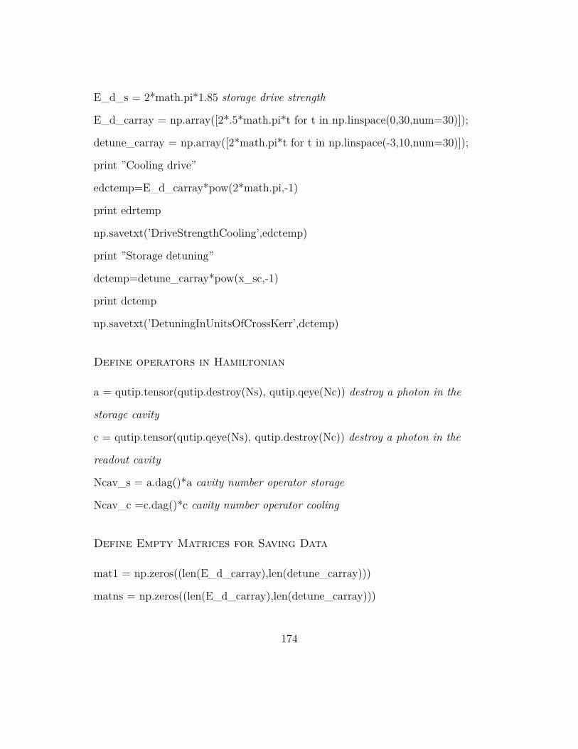
E_d_s = 2*math.pi*1.85 storage drive strength
E_d_carray = np.array([2*.5*math.pi*t for t in np.linspace(0,30,num=30)]);
detune_carray = np.array([2*math.pi*t for t in np.linspace(-3,10,num=30)]);
print ”Cooling drive”
edctemp=E_d_carray*pow(2*math.pi,-1)
print edrtemp
np.savetxt(’DriveStrengthCooling’,edctemp)
print ”Storage detuning”
dctemp=detune_carray*pow(x_sc,-1)
print dctemp
np.savetxt(’DetuningInUnitsOfCrossKerr’,dctemp)
Define operators in Hamiltonian
a = qutip.tensor(qutip.destroy(Ns), qutip.qeye(Nc)) destroy a photon in the
storage cavity
c = qutip.tensor(qutip.qeye(Ns), qutip.destroy(Nc)) destroy a photon in the
readout cavity
Ncav_s = a.dag()*a cavity number operator storage
Ncav_c =c.dag()*c cavity number operator cooling
Define Empty Matrices for Saving Data
mat1 = np.zeros((len(E_d_carray),len(detune_carray)))
matns = np.zeros((len(E_d_carray),len(detune_carray)))
174

matnc = np.zeros((len(E_d_carray),len(detune_carray)))
mat0 = np.zeros((len(E_d_carray),len(detune_carray)))
mat2 = np.zeros((len(E_d_carray),len(detune_carray)))
mat3 = np.zeros((len(E_d_carray),len(detune_carray)))
for ix in range(len(E_d_carray)):
print ’ix = %d’ % ix
for iy in range(len(detune_carray)):
H = detune_s*Ncav_s+detune_carray[iy]*Ncav_r+.5*Kerr_s*a.dag()*a.dag()*a*a+.5*Kerr_r*b.dag()*b.dag()*b*b
+x_sr*a.dag()*a*b.dag()*b+E_d_s*(a.dag()+a)+E_d_carray[ix]*(b.dag()+b)
final_state = qutip.steadystate(H, c_ops)
val1 = qutip.expect(qutip.fock_dm(Ns,1),qutip.ptrace(final_state,0))
val0 = qutip.expect(qutip.fock_dm(Ns,0),qutip.ptrace(final_state,0))
val2 = qutip.expect(qutip.fock_dm(Ns,2),qutip.ptrace(final_state,0))
val3 = qutip.expect(qutip.fock_dm(Ns,3),qutip.ptrace(final_state,0))
valns = qutip.expect(Ncav_s,final_state)
valnc = qutip.expect(Ncav_c,final_state)
mat1[ix,iy] = round(val1,4)
mat0[ix,iy] = round(val0,4)
mat2[ix,iy] = round(val2,4)
mat3[ix,iy] = round(val3,4)
matns[ix,iy] = round(valns,4)
matnc[ix,iy] = round(valnc,4)
print ”Probability 1fock”
175

print mat1
np.savetxt(’PopN1’,mat1)
print ”Probability 0fock”
print mat0
np.savetxt(’PopN0’,mat0)
print ”Probability 2fock”
print mat2
np.savetxt(’PopN2’,mat2)
print ”Probability 3fock”
print mat3
np.savetxt(’PopN3’,mat3)
print ”Nbar in storage”
print matns
np.savetxt(’NbarStorage’,matns)
print ”Nbar in cooling”
print matnc
np.savetxt(’NbarCooling’,matnc)
176

Bibliography
[1] E. Schrödinger, Brit. J. Phil. Sci. 3, 233 (1952).
[2] A. J. Leggett, Le Journal de Physique Colloques 39, C6 (1978).
[3] A. J. Leggett, Prog. of Theor. Phys. (Suppl.) 69, 80 (1980).
[4] A. O. Caldeira and A. J. Leggett, Ann. Phys. 149, 374 (1983).
[5] M. H. Devoret, J. M. Martinis, D. Esteve, and J. Clarke, Phys. Rev. Lett.53, 1260 (1984).
[6] M. H. Devoret, J. M. Martinis, and J. Clarke, Phys. Rev. Lett. 55, 1908(1985).
[7] D. Esteve, M. H. Devoret, and J. M. Martinis, Phys. Rev. B 34, 158(1986).
[8] J. M. Martinis, M. H. Devoret, and J. Clarke, Phys. Rev. Lett. 55, 1543(1985).
[9] J. M. Martinis, M. H. Devoret, and J. Clarke, Phys. Rev. B 35, 4682(1987).
[10] Y. Nakamura, Y. A. Pashkin, and J. S. Tsai, Nature 398, 786 (1999).
[11] J. E. Mooij, T. P. Orlando, L. Levitov, L. Tian, C. H. Van der Wal, andS. Lloyd, Science 285, 1036 (1999).
[12] R. P. Feynman, International Journal of Theoretical Physics 21, 467(1982).
[13] D. Deutsch, in Proceedings of the Royal Society of London A: Mathemati-cal, Physical and Engineering Sciences, Vol. 400 (The Royal Society, 1985)pp. 97–117.
177

[14] D. Deutsch and R. Jozsa, in Proceedings of the Royal Society of LondonA: Mathematical, Physical and Engineering Sciences, Vol. 439 (The RoyalSociety, 1992) pp. 553–558.
[15] P. W. Shor, in Foundations of Computer Science, 1994 Proceedings., 35thAnnual Symposium on (IEEE, 1994) pp. 124–134.
[16] P. W. Shor, Phys. Rev. A 52, R2493 (1995).
[17] P. W. Shor, in Foundations of Computer Science, 1996. Proceedings., 37thAnnual Symposium on (IEEE, 1996) pp. 56–65.
[18] P. W. Shor, SIAM Journal on Computing 26, 1484 (1997).
[19] A. Steane, in Proceedings of the Royal Society of London A: Mathematical,Physical and Engineering Sciences, Vol. 452 (The Royal Society, 1996) pp.2551–2577.
[20] A. M. Steane, Phys. Rev. Lett. 78, 2252 (1997).
[21] R. Laflamme, C. Miquel, J. P. Paz, and W. H. Zurek, Phys. Rev. Lett.77, 198 (1996).
[22] M. A. Nielsen and I. L. Chuang, Quantum computation and quantum in-formation (Cambridge university press, 2010).
[23] I. L. Chuang, L. M. Vandersypen, X. Zhou, D. W. Leung, and S. Lloyd,Nature 393, 143 (1998).
[24] I. L. Chuang, N. Gershenfeld, and M. Kubinec, Phys. Rev. Lett. 80, 3408(1998).
[25] J. A. Jones, M. Mosca, and R. H. Hansen, Nature 393, 344 (1998).
[26] L. M. K. Vandersypen, M. Steffen, G. Breyta, C. S. Yannoni, M. H. Sher-wood, and I. L. Chuang, Nature 414, 883 (2001).
[27] W. S. Warren, Science 277, 1688 (1997).
[28] J. I. Cirac and P. Zoller, Phys. Rev. Lett. 74, 4091 (1995).
[29] D. Leibfried, R. Blatt, C. Monroe, and D. Wineland, Reviews of ModernPhysics 75, 281 (2003).
178

[30] D. Leibfried, B. DeMarco, V. Meyer, D. Lucas, M. Barrett, J. Britton,W. M. Itano, B. Jelenković, C. Langer, T. Rosenband, et al., Nature 422,412 (2003).
[31] D. Kielpinski, C. Monroe, and D. J. Wineland, Nature 417, 709 (2002).
[32] T. Monz, P. Schindler, J. T. Barreiro, M. Chwalla, D. Nigg, W. A. Coish,M. Harlander, W. Hänsel, M. Hennrich, and R. Blatt, Phys. Rev. Lett.106, 130506 (2011).
[33] H.-J. Briegel, T. Calarco, D. Jaksch, J. I. Cirac, and P. Zoller, Journal ofmodern optics 47, 415 (2000).
[34] D. Loss and D. P. DiVincenzo, Physical Review A 57, 120 (1998).
[35] R. Hanson, L. Kouwenhoven, J. Petta, S. Tarucha, and L. Vandersypen,Rev. Mod. Phys. 79, 1217 (2007).
[36] B. M. Maune, M. G. Borselli, B. Huang, T. D. Ladd, P. W. Deelman,K. S. Holabird, A. A. Kiselev, I. Alvarado-Rodriguez, R. S. Ross, A. E.Schmitz, et al., Nature 481, 344 (2012).
[37] M. D. Shulman, O. E. Dial, S. P. Harvey, H. Bluhm, V. Umansky, andA. Yacoby, Science 336, 202 (2012).
[38] D. D. Awschalom, L. C. Bassett, A. S. Dzurak, E. L. Hu, and J. R. Petta,Science 339, 1174 (2013).
[39] F. Jelezko and J. Wrachtrup, PHYSICA STATUS SOLIDI A APPLICA-TIONS AND MATERIALS SCIENCE 203, 3207 (2006).
[40] M. V. G. Dutt, L. Childress, L. Jiang, E. Togan, J. Maze, F. Jelezko,A. S. Zibrov, P. R. Hemmer, and M. D. Lukin, Science 316, 1312 (2007).
[41] P. C. Maurer, G. Kucsko, C. Latta, L. Jiang, N. Y. Yao, S. D. Bennett,F. Pastawski, D. Hunger, N. Chisholm, M. Markham, et al., Science 336,1283 (2012).
[42] W. Pfaff, T. H. Taminiau, L. Robledo, H. Bernien, M. Markham, D. J.Twitchen, and R. Hanson, Nature Physics 9, 29 (2013).
179
[43] W. Pfaff, B. Hensen, H. Bernien, S. B. van Dam, M. S. Blok, T. H.Taminiau, M. J. Tiggelman, R. N. Schouten, M. Markham, D. J.Twitchen, et al., Science 345, 532 (2014).
[44] M. H. Devoret and R. J. Schoelkopf, Science 339, 1169 (2013).
[45] B. R. Johnson, M. D. Reed, A. A. Houck, D. I. Schuster, L. S. Bishop,E. Ginossar, J. M. Gambetta, L. DiCarlo, L. Frunzio, S. M. Girvin, et al.,Nature Phys. 6, 663 (2010).
[46] M. Hatridge, S. Shankar, M. Mirrahimi, F. Schackert, K. Geerlings,T. Brecht, K. M. Sliwa, B. Abdo, L. Frunzio, S. M. Girvin, et al., Science339, 178 (2013).
[47] A. A. Houck, J. Koch, M. H. Devoret, S. M. Girvin, and R. J. Schoelkopf,Quantum Information Processing 8, 105 (2009).
[48] D. M. Pozar, Microwave Engineering, 3rd ed. (John Wiley & Sons, Inc.,2005).
[49] R. P. Feynman, R. B. Leighton, and M. Sands, The Feynman Lectures onPhysics, Vol. 2 (Basic Books, 2013).
[50] M. Reagor, W. Pfaff, R. Heeres, N. Ofek, K. Chou, J. Blumoff, Z. Legh-tas, S. Touzard, K. Sliwa, E. T. Holland, et al., Bulletin of the AmericanPhysical Society 60 (2015).
[51] W. Pfaff, M. Reagor, R. Heeres, N. Ofek, K. Chou, J. Blumoff, Z. Legh-tas, S. Touzard, K. Sliwa, E. T. Holland, et al., Bulletin of the AmericanPhysical Society 60 (2015).
[52] M. Reagor, W. Pfaff, C. Axline, R. W. Heeres, N. Ofek, K. Sliwa, E. T.Holland, C. Wang, J. Blumoff, K. Chou, M. J. Hatridge, L. Frunzio, M. H.Devoret, L. Jiang, and R. J. Schoelkopf, (2015), 1508.05882 .
[53] R. W. Heeres, B. Vlastakis, E. T. Holland, S. Krastanov, V. V. Al-bert, L. Frunzio, L. Jiang, and R. J. Schoelkopf, arXiv preprintarXiv:1503.01496 (2015).
[54] S. Krastanov, V. V. Albert, C. Shen, C.-L. Zou, R. W. Heeres, B. Vlas-takis, R. J. Schoelkopf, and L. Jiang, arXiv preprint arXiv:1502.08015(2015), 1502.08015 .
180

[55] R. Barends, N. Vercruyssen, A. Endo, P. J. de Visser, T. Zijlstra, T. M.Klapwijk, P. Diener, S. J. C. Yates, and J. J. A. Baselmans, Appl. Phys.Lett. 97, 023508 (2010).
[56] M. R. Vissers, J. S. Kline, J. Gao, D. S. Wisbey, and D. P. Pappas, Appl.Phys. Lett. 100, 082602 (2012).
[57] A. Bruno, G. de Lange, S. Asaad, K. L. van der Enden, N. K. Langford,and L. DiCarlo, Appl. Phys. Lett. 106, 182601 (2015).
[58] M. J. Reagor, H. Paik, G. Catelani, L. Sun, C. Axline, E. T. Holland,I. M. Pop, N. A. Masluk, T. Brecht, L. Frunzio, et al., Appl. Phys. Lett.102, 192604 (2013).
[59] J. M. Raimond, T. Meunier, P. Bertet, S. Gleyzes, P. Maioli, A. Auffeves,G. Nogues, M. Brune, and S. Haroche, J. Phys. B: At. Mol. Opt. Phys.38, S535 (2005).
[60] T. K. Sarkar, R. Mailloux, A. A. Oliner, M. Salazar-Palma, and D. L.Sengupta, History of Wireless, Vol. 177 (John Wiley & Sons, 2006).
[61] H. H. Howe, Stripline Circuit Design (Artech House Dedham, MA, 1974).
[62] H. Paik, D. I. Schuster, L. S. Bishop, G. Kirchmair, G. Catelani, A. P.Sears, B. R. Johnson, M. J. Reagor, L. Frunzio, L. I. Glazman, et al.,Phys. Rev. Lett. 107, 240501 (2011).
[63] A. P. Sears, A. Petrenko, G. Catelani, L. Sun, H. Paik, G. Kirchmair,L. Frunzio, L. I. Glazman, S. M. Girvin, and R. J. Schoelkopf, Phys. Rev.B 86, 180504 (2012).
[64] A. P. Sears, Extending Coherence in Superconducting Qubits: From mi-croseconds to milliseconds, Ph.D. thesis, Yale University (2013).
[65] B. Bhat and S. K. Koul, Stripline-like transmission lines for microwaveintegrated circuits (New Age International, 1989).
[66] G. Catelani, Private Communications.
[67] S. B. Nam, Phys. Rev. 156, 470 (1967).
[68] S. B. Nam, Phys. Rev. 156, 487 (1967).
181

[69] J. P. Turneaure and I. Weissman, J. Appl. Phys. 39, 4417 (1968).
[70] J. P. Turneaure, J. Halbritter, and H. A. Schwettman, JOSC 4, 341(1991).
[71] L. D. Landau and E. M. Lifshitz, Course of theoretical physics, Vol. 10(Elsevier, 2013).
[72] M. Tinkham, Introduction to Superconductivity (Courier Corporation,2012).
[73] C. Axline, M. J. Reagor, K. Shain, P. Reinhold, T. Brecht, E. T. Hol-land, C. Wang, R. Heeres, L. Frunzio, and R. J. Schoelkopf, Bulletin ofthe American Physical Society 60 (2015).
[74] T. Brecht, C. Wang, C. Axline, M. J. Reagor, M. Hatridge, P. Reinhold,L. Frunzio, and R. J. Schoelkopf, Bulletin of the American Physical Soci-ety 59 (2014).
[75] M. Fox, Quantum Optics: An Introduction (Oxford University Press,2006).
[76] C. Gerry and P. Knight, Introductory Quantum Optics (Cambridge Uni-versity Press, 2005).
[77] D. F. Walls and G. J. Milburn, Quantum Optics (Springer Science & Busi-ness Media, 2007).
[78] H. Mabuchi and A. C. Doherty, Science 298, 1372 (2002).
[79] E. T. Jaynes and F. W. Cummings, Proceedings of the IEEE 51, 89(1963).
[80] F. W. Cummings, Phys. Rev. 140, A1051 (1965).
[81] R. J. Schoelkopf and S. M. Girvin, Nature 451, 664 (2008).
[82] R. J. Thompson, G. Rempe, and H. J. Kimble, Physical Review Letters68, 1132 (1992).
[83] L. S. Bishop, J. M. Chow, J. Koch, A. A. Houck, M. H. Devoret,E. Thuneberg, S. M. Girvin, and R. J. Schoelkopf, Nature Physics 5, 105(2009).
182

[84] S. Haroche and J. M. Raimond, Exploring the Quantum (Oxford Univ.Press, 2006).
[85] J.-M. Raimond, M. Brune, and S. Haroche, Reviews of Modern Physics73, 565 (2001).
[86] MinutePhysics, “2012 noble prize physics,” .
[87] S. Gleyzes, S. Kuhr, C. Guerlin, J. Bernu, S. Deleglise, U. B. Hoff,M. Brune, J.-M. Raimond, and S. Haroche, Nature 446, 297 (2007).
[88] J. Koch, M. Y. Terri, J. Gambetta, A. A. Houck, D. I. Schuster, J. Majer,A. Blais, M. H. Devoret, S. M. Girvin, and R. J. Schoelkopf, Phys. Rev.A 76, 042319 (2007).
[89] J. Schreier, A. A. Houck, J. Koch, D. I. Schuster, B. Johnson, J. Chow,J. M. Gambetta, J. Majer, L. Frunzio, M. H. Devoret, et al., Physical Re-view B 77, 180502 (2008).
[90] D. I. Schuster, Circuit Quantum Electrodynamics, Ph.D. thesis, Yale Uni-versity (2007).
[91] V. E. Manucharyan, J. Koch, L. I. Glazman, and M. H. Devoret, Science326, 113 (2009).
[92] V. E. Manucharyan, Superinductance, Ph.D. thesis, Yale University(2012).
[93] V. Bouchiat, D. Vion, P. Joyez, D. Esteve, and M. H. Devoret, PhysicaScripta 1998, 165 (1998).
[94] M. H. Devoret, Les Houches, Session LXIII (1995).
[95] L. S. Bishop, Circuit Quantum Electrodynamics, Ph.D. thesis, Yale Uni-versity (2010).
[96] S. M. Girvin, Circuit QED: Superconducting Qubits Coupled to MicrowavePhotons (Oxford University Press, 2012).
[97] A. Blais, R.-S. Huang, A. Wallraff, S. M. Girvin, and R. J. Schoelkopf,Physical Review A 69, 062320 (2004).
183

[98] A. Wallraff, D. I. Schuster, A. Blais, L. Frunzio, R.-S. Huang, J. Majer,S. Kumar, S. M. Girvin, and R. J. Schoelkopf, Nature 431, 162 (2004).
[99] K. Geerlings, Z. Leghtas, I. M. Pop, S. Shankar, L. Frunzio, R. J.Schoelkopf, M. Mirrahimi, and M. H. Devoret, Phys. Rev. Lett. 110,120501 (2013).
[100] S. E. Nigg, H. Paik, B. Vlastakis, G. Kirchmair, S. Shankar, L. Frunzio,M. H. Devoret, R. J. Schoelkopf, and S. M. Girvin, Phys. Rev. Lett. 108,240502 (2012).
[101] J. Johansson, P. Nation, and F. Nori, Comput. Phys. Commun. 184,1234 (2013).
[102] J. Niemeyer and V. Kose, Appl. Phys. Lett. 29, 380 (1976).
[103] G. J. Dolan, Appl. Phys. Lett. 31, 337 (1977).
[104] K. L. Geerlings, Improving Coherence of Superconducting Qubits and Res-onators, Ph.D. thesis, Yale University (2013).
[105] A. Wallraff, D. I. Schuster, A. Blais, L. Frunzio, J. Majer, M. H. Devoret,S. M. Girvin, and R. J. Schoelkopf, Phys. Rev. Lett. 95, 060501 (2005).
[106] R. Vijay, D. H. Slichter, and I. Siddiqi, Phys. Rev. Lett. 106, 110502(2011).
[107] R. Vijay, C. Macklin, D. H. Slichter, S. J. Weber, K. Murch, R. Naik,A. N. Korotkov, and I. Siddiqi, Nature 490, 77 (2012).
[108] L. Sun, A. Petrenko, Z. Leghtas, B. Vlastakis, G. Kirchmair, K. M. Sliwa,A. Narla, M. Hatridge, S. Shankar, J. Blumoff, L. Frunzio, M. Mirrahimi,M. H. Devoret, and R. J. Schoelkopf, Nature 511, 444 (2014).
[109] J. Kelly, R. Barends, A. G. Fowler, A. Megrant, E. Jeffrey, T. C. White,D. Sank, J. Y. Mutus, B. Campbell, Y. Chen, Z. Chen, B. Chiaro,A. Dunsworth, I. C. Hoi, C. Neill, P. J. J. O’Malley, C. Quintana,P. Roushan, A. Vainsencher, J. Wenner, A. N. Cleland, and J. M. Mar-tinis, Nature 519, 66 (2015).
[110] D. Ristè, C. C. Bultink, K. W. Lehnert, and L. DiCarlo, Phys. Rev. Lett.109, 240502 (2012).
184

[111] D. Ristè, M. Dukalski, C. A. Watson, G. de Lange, M. J. Tiggelman,Y. M. Blanter, K. W. Lehnert, R. N. Schouten, and L. DiCarlo, Nature502, 350 (2013).
[112] D. Riste, S. Poletto, M. Z. Huang, A. Bruno, V. Vesterinen, O. P. Saira,and L. DiCarlo, Nat. Commun. 6 (2015).
[113] B. Vlastakis, A. Petrenko, N. Ofek, L. Sun, Z. Leghtas, K. Sliwa,Y. Liu, M. Hatridge, J. Blumoff, L. Frunzio, et al., arXiv preprintarXiv:1504.02512 (2015).
[114] A. D. Córcoles, E. Magesan, S. J. Srinivasan, A. W. Cross, M. Steffen,J. M. Gambetta, and J. M. Chow, Nat. Commun. 6 (2015).
[115] M. D. Reed, L. DiCarlo, B. R. Johnson, L. Sun, D. I. Schuster, L. Frunzio,and R. J. Schoelkopf, Phys. Rev. Lett. 105, 173601 (2010).
[116] H. Wiseman, Phys. Rev. A 49, 2133 (1994).
[117] A. C. Doherty, S. Habib, K. Jacobs, H. Mabuchi, and S. M. Tan, Phys.Rev. A 62, 012105 (2000).
[118] H. M. Wiseman and G. J. Milburn, Quantum Measurement and Control(Cambridge University Press, 2009).
[119] R. J. Nelson, Y. Weinstein, D. Cory, and S. Lloyd, Phys. Rev. Lett. 85,3045 (2000).
[120] W. P. Smith, J. E. Reiner, L. A. Orozco, S. Kuhr, and H. M. Wiseman,Phys. Rev. Lett. 89, 133601 (2002).
[121] R. L. Cook, P. J. Martin, and J. M. Geremia, Nature 446, 774 (2007).
[122] G. Gillett, R. Dalton, B. Lanyon, M. Almeida, M. Barbieri, G. J. Pryde,J. O’brien, K. Resch, S. Bartlett, and A. White, Phys. Rev. Lett. 104,080503 (2010).
[123] J. M. Geremia, Phys. Rev. Lett. 97, 073601 (2006).
[124] I. Dotsenko, M. Mirrahimi, M. Brune, S. Haroche, J.-M. Raimond, andP. Rouchon, Physical Review A 80, 013805 (2009).
185

[125] C. Sayrin, I. Dotsenko, X. Zhou, B. Peaudecerf, T. Rybarczyk, S. Gleyzes,P. Rouchon, M. Mirrahimi, H. Amini, M. Brune, et al., Nature 477, 73(2011).
[126] X. Zhou, I. Dotsenko, B. Peaudecerf, T. Rybarczyk, C. Sayrin, S. Gleyzes,J. M. Raimond, M. Brune, and S. Haroche, Phys. Rev. Lett. 108, 243602(2012).
[127] B. Peaudecerf, C. Sayrin, X. Zhou, T. Rybarczyk, S. Gleyzes, I. Dotsenko,J. Raimond, M. Brune, and S. Haroche, Phys. Rev. A 87, 042320 (2013).
[128] S. Brakhane, W. Alt, T. Kampschulte, M. Martinez-Dorantes,R. Reimann, S. Yoon, A. Widera, and D. Meschede, Phys. Rev. Lett.109, 173601 (2012).
[129] M. Blok, C. Bonato, M. Markham, D. Twitchen, V. Dobrovitski, andR. Hanson, Nature Physics 10, 189 (2014).
[130] W. Cui and F. Nori, Physical Review A 88, 063823 (2013).
[131] G. De Lange, D. Riste, M. Tiggelman, C. Eichler, L. Tornberg, G. Jo-hansson, A. Wallraff, R. Schouten, and L. DiCarlo, Phys. Rev. Lett. 112,080501 (2014).
[132] P. Schindler, T. Monz, D. Nigg, J. T. Barreiro, E. A. Martinez, M. F.Brandl, M. Chwalla, M. Hennrich, and R. Blatt, Phys. Rev. Lett. 110,070403 (2013).
[133] P. Campagne-Ibarcq, E. Flurin, N. Roch, D. Darson, P. Morfin, M. Mir-rahimi, M. H. Devoret, F. Mallet, and B. Huard, Phys. Rev. X 3, 021008(2013).
[134] N. Roch, M. E. Schwartz, F. Motzoi, C. Macklin, R. Vijay, A. W. Eddins,A. N. Korotkov, K. B. Whaley, M. Sarovar, and I. Siddiqi, Phys. Rev.Lett. 112, 170501 (2014).
[135] A. R. Calderbank and P. W. Shor, Phys. Rev. A 54, 1098 (1996).
[136] M. Mirrahimi, Z. Leghtas, V. V. Albert, S. Touzard, R. J. Schoelkopf,L. Jiang, and M. H. Devoret, New J. Phys. 16, 045014 (2014).
186

[137] B. Vlastakis, G. Kirchmair, Z. Leghtas, S. E. Nigg, L. Frunzio, S. M.Girvin, M. Mirrahimi, M. H. Devoret, and R. J. Schoelkopf, Science 342,607 (2013).
[138] S. B. Bravyi and A. Y. Kitaev, arXiv preprint quant-ph/9811052 (1998).
[139] A. Y. Kitaev, Ann. Phys. 303, 2 (2003).
[140] R. Raussendorf and J. Harrington, Phys. Rev. Lett. 98, 190504 (2007).
[141] A. G. Fowler, A. M. Stephens, and P. Groszkowski, Phys. Rev. A 80,052312 (2009).
[142] A. G. Fowler, M. Mariantoni, J. M. Martinis, and A. N. Cleland, Phys.Rev. A 86, 032324 (2012).
[143] R. Barends, J. Kelly, A. Megrant, A. Veitia, D. Sank, E. Jeffrey, T. White,J. Mutus, A. Fowler, B. Campbell, et al., Nature 508, 500 (2014).
[144] J. M. Chow, J. M. Gambetta, E. Magesan, D. W. Abraham, A. W. Cross,B. R. Johnson, N. A. Masluk, C. A. Ryan, J. A. Smolin, S. J. Srinivasan,et al., Nat. Commun. 5 (2014).
[145] J. F. Poyatos, J. I. Cirac, and P. Zoller, Phys. Rev. Lett. 77, 4728 (1996).
[146] S. Diehl, A. Micheli, A. Kantian, B. Kraus, H. Büchler, and P. Zoller,Nature Phys. 4, 878 (2008).
[147] B. Kraus, H. P. Büchler, S. Diehl, A. Kantian, A. Micheli, and P. Zoller,Phys. Rev. A 78, 042307 (2008).
[148] C. A. Muschik, E. S. Polzik, and J. I. Cirac, Phys. Rev. A 83, 052312(2011).
[149] H. Krauter, C. A. Muschik, K. Jensen, W. Wasilewski, J. M. Petersen,J. I. Cirac, and E. S. Polzik, Phys. Rev. Lett. 107, 080503 (2011).
[150] A. Sarlette, J.-M. Raimond, M. Brune, and P. Rouchon, Phys. Rev. Lett.107, 010402 (2011).
[151] J. T. Barreiro, M. Müller, P. Schindler, D. Nigg, T. Monz, M. Chwalla,M. Hennrich, C. F. Roos, P. Zoller, and R. Blatt, Nature 470, 486(2011).
187
[152] C. A. Muschik, H. Krauter, K. Jensen, J. M. Petersen, J. I. Cirac, andE. S. Polzik, J. Phys. B: At. Mol. Opt. Phys. 45, 124021 (2012).
[153] K. Vollbrecht, C. A. Muschik, and J. I. Cirac, Phys. Rev. Lett. 107,120502 (2011).
[154] Z. Leghtas, U. Vool, S. Shankar, M. Hatridge, S. M. Girvin, M. H. De-voret, and M. Mirrahimi, Phys. Rev. A 88, 023849 (2013).
[155] S. Shankar, M. Hatridge, Z. Leghtas, K. Sliwa, A. Narla, U. Vool, S. M.Girvin, L. Frunzio, M. Mirrahimi, and M. H. Devoret, Nature 504, 419(2013).
[156] Y. Lin, J. P. Gaebler, F. Reiter, T. R. Tan, R. Bowler, A. S. Sørensen,D. Leibfried, and D. J. Wineland, Nature 504, 415 (2013).
[157] Z. Leghtas, S. Touzard, I. M. Pop, A. Kou, B. Vlastakis, A. Petrenko,K. M. Sliwa, A. Narla, S. Shankar, M. J. Hatridge, M. Reagor, L. Frun-zio, R. J. Schoelkopf, M. Mirrahimi, and M. H. Devoret, Science 347, 853(2015).
[158] A. Roy, Z. Leghtas, A. D. Stone, M. H. Devoret, and M. Mirrahimi, Phys.Rev. A 91, 013810 (2015).
[159] J. Cohen and M. Mirrahimi, Phys. Rev. A 90, 062344 (2014).
[160] V. V. Albert, S. Krastanov, C. Shen, R.-B. Liu, R. J. Schoelkopf, M. Mir-rahimi, M. H. Devoret, and L. Jiang, arXiv preprint arXiv:1503.00194(2015), 1503.00194 .
[161] K. W. Murch, U. Vool, D. Zhou, S. J. Weber, S. M. Girvin, and I. Sid-diqi, Phys. Rev. Lett. 109, 183602 (2012).
[162] A. Metelmann and A. A. Clerk, Phys. Rev. Lett. 112, 133904 (2014).
[163] A. Metelmann and A. A. Clerk, arXiv preprint arXiv:1502.07274 (2015).
[164] C. Aron, M. Kulkarni, and H. E. Türeci, Phys. Rev. A 90, 062305 (2014).
[165] K. Børkje, Phys. Rev. A 90, 023806 (2014).
[166] M. J. Kastoryano, M. M. Wolf, and J. Eisert, Phys. Rev. Lett. 110,110501 (2013).
188

[167] G. Kirchmair, B. Vlastakis, Z. Leghtas, S. E. Nigg, H. Paik, E. Ginossar,M. Mirrahimi, L. Frunzio, S. M. Girvin, and R. J. Schoelkopf, Nature495, 205 (2013).
[168] Y. Hu, G.-Q. Ge, S. Chen, X.-F. Yang, and Y.-L. Chen, Phys. Rev. A 84,012329 (2011).
[169] J. Gambetta, A. Blais, D. I. Schuster, A. Wallraff, L. Frunzio, J. Majer,M. H. Devoret, S. M. Girvin, and R. J. Schoelkopf, Phys. Rev. A 74,042318 (2006).
[170] A. A. Clerk, M. H. Devoret, S. M. Girvin, F. Marquardt, and R. J.Schoelkopf, Rev. Mod. Phys. 82, 1155 (2010).
189