Embed Size (px)
Citation preview
SCHS279D − DECEMBER 1998 − REVISED OCTOBER 2003
1POST OFFICE BOX 655303 • DALLAS, TEXAS 75265
2-V to 6-V VCC Operation (’HC4511)
4.5-V to 5.5-V VCC Operation(CD74HCT4511)
High-Output Sourcing Capability− 7.5 mA at 4.5 V (CD74HCT4511)− 10 mA at 6 V (’HC4511)
Input Latches for BCD Code Storage
Lamp Test and Blanking Capability
Balanced Propagation Delays andTransition Times
Significant Power Reduction Compared toLSTTL Logic ICs
’HC4511− High Noise Immunity,
NIL or NIH = 30% of VCC at VCC = 5 V
CD74HCT4511− Direct LSTTL Input Logic Compatibility,
VIL = 0.8 V Maximum, V IH = 2 V Minimum− CMOS Input Compatibility, I I ≤ 1 µA
at VOL, VOH
description/ordering information
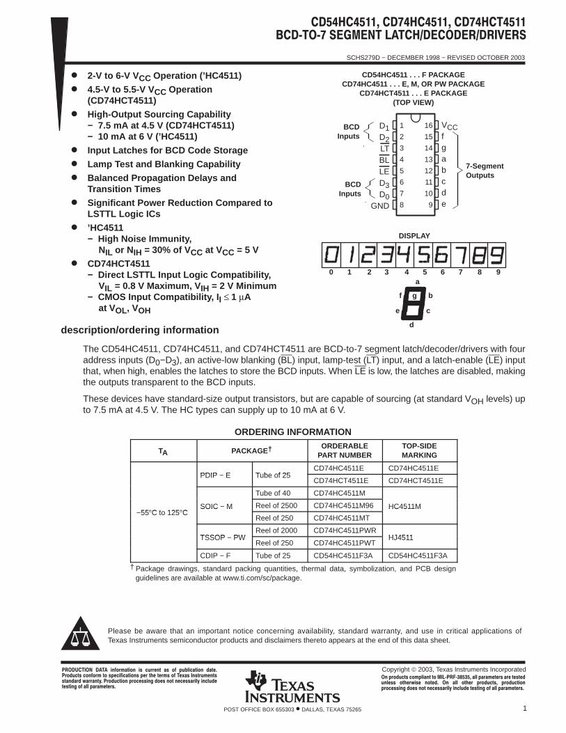
The CD54HC4511, CD74HC4511, and CD74HCT4511 are BCD-to-7 segment latch/decoder/drivers with fouraddress inputs (D0−D3), an active-low blanking (BL) input, lamp-test (LT) input, and a latch-enable (LE) inputthat, when high, enables the latches to store the BCD inputs. When LE is low, the latches are disabled, makingthe outputs transparent to the BCD inputs.
These devices have standard-size output transistors, but are capable of sourcing (at standard VOH levels) upto 7.5 mA at 4.5 V. The HC types can supply up to 10 mA at 6 V.
ORDERING INFORMATION
TA PACKAGE † ORDERABLEPART NUMBER
TOP-SIDEMARKING
PDIP − E Tube of 25CD74HC4511E CD74HC4511E
PDIP − E Tube of 25CD74HCT4511E CD74HCT4511E
Tube of 40 CD74HC4511M
−55°C to 125°CSOIC − M Reel of 2500 CD74HC4511M96 HC4511M
−55°C to 125°CSOIC − M
Reel of 250 CD74HC4511MT
HC4511M
TSSOP − PWReel of 2000 CD74HC4511PWR
HJ4511TSSOP − PWReel of 250 CD74HC4511PWT
HJ4511
CDIP − F Tube of 25 CD54HC4511F3A CD54HC4511F3A
† Package drawings, standard packing quantities, thermal data, symbolization, and PCB designguidelines are available at www.ti.com/sc/package.
Copyright 2003, Texas Instruments Incorporated !" # $%&" !# '%()$!" *!"&+*%$"# $ " #'&$$!"# '& ",& "&# &-!# #"%&"##"!*!* .!!"/+ *%$" '$&##0 *&# " &$&##!)/ $)%*&"&#"0 !)) '!!&"&#+
Please be aware that an important notice concerning availability, standard warranty, and use in critical applications ofTexas Instruments semiconductor products and disclaimers thereto appears at the end of this data sheet.
1
2
3
4
5
6
7
8
16
15
14
13
12
11
10
9
D1D2LTBLLED3D0
GND
VCCfgabcde
BCDInputs
BCDInputs
7-SegmentOutputs
CD54HC4511 . . . F PACKAGECD74HC4511 . . . E, M, OR PW PACKAGE
CD74HCT4511 . . . E PACKAGE(TOP VIEW)
0 1 2 3 4 5 6 7 8 9
DISPLAY
a
b
c
d
e
f g
'*%$"# $')!" " 1232 !)) '!!&"&# !& "&#"&*%)&## ",&.#& "&*+ !)) ",& '*%$"# '*%$"'$&##0 *&# " &$&##!)/ $)%*& "&#"0 !)) '!!&"&#+
SCHS279D − DECEMBER 1998 − REVISED OCTOBER 2003
2 POST OFFICE BOX 655303 • DALLAS, TEXAS 75265
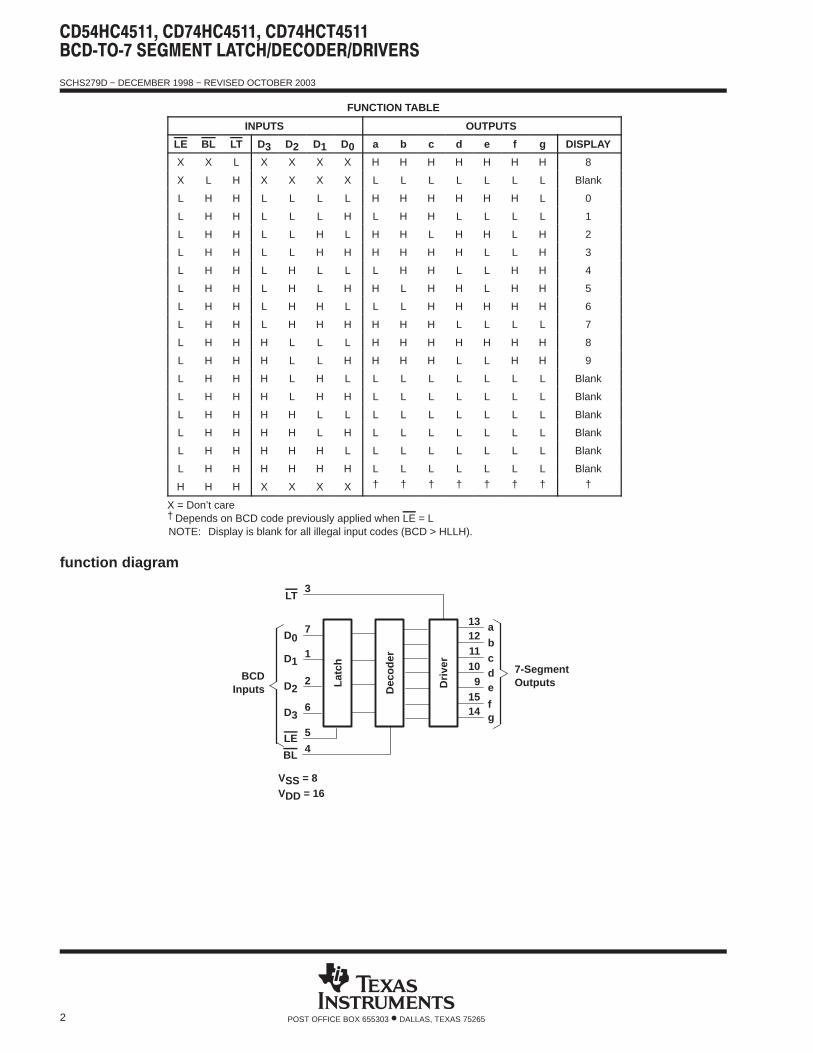
FUNCTION TABLE
INPUTS OUTPUTS
LE BL LT D3 D2 D1 D0 a b c d e f g DISPLAY
X X L X X X X H H H H H H H 8
X L H X X X X L L L L L L L Blank
L H H L L L L H H H H H H L 0
L H H L L L H L H H L L L L 1
L H H L L H L H H L H H L H 2
L H H L L H H H H H H L L H 3
L H H L H L L L H H L L H H 4
L H H L H L H H L H H L H H 5
L H H L H H L L L H H H H H 6
L H H L H H H H H H L L L L 7
L H H H L L L H H H H H H H 8
L H H H L L H H H H L L H H 9
L H H H L H L L L L L L L L Blank
L H H H L H H L L L L L L L Blank
L H H H H L L L L L L L L L Blank
L H H H H L H L L L L L L L Blank
L H H H H H L L L L L L L L Blank
L H H H H H H L L L L L L L Blank
H H H X X X X † † † † † † † †
X = Don’t care† Depends on BCD code previously applied when LE = LNOTE: Display is blank for all illegal input codes (BCD > HLLH).
function diagram
7
1
2
6
5
4
D0
D1
D2
D3
LE
BL
LT3
VSS = 8VDD = 16
13121110
91514
abcde
fg
Latc
h
Dec
oder
Driv
er 7-SegmentOutputs
BCDInputs
SCHS279D − DECEMBER 1998 − REVISED OCTOBER 2003
3POST OFFICE BOX 655303 • DALLAS, TEXAS 75265
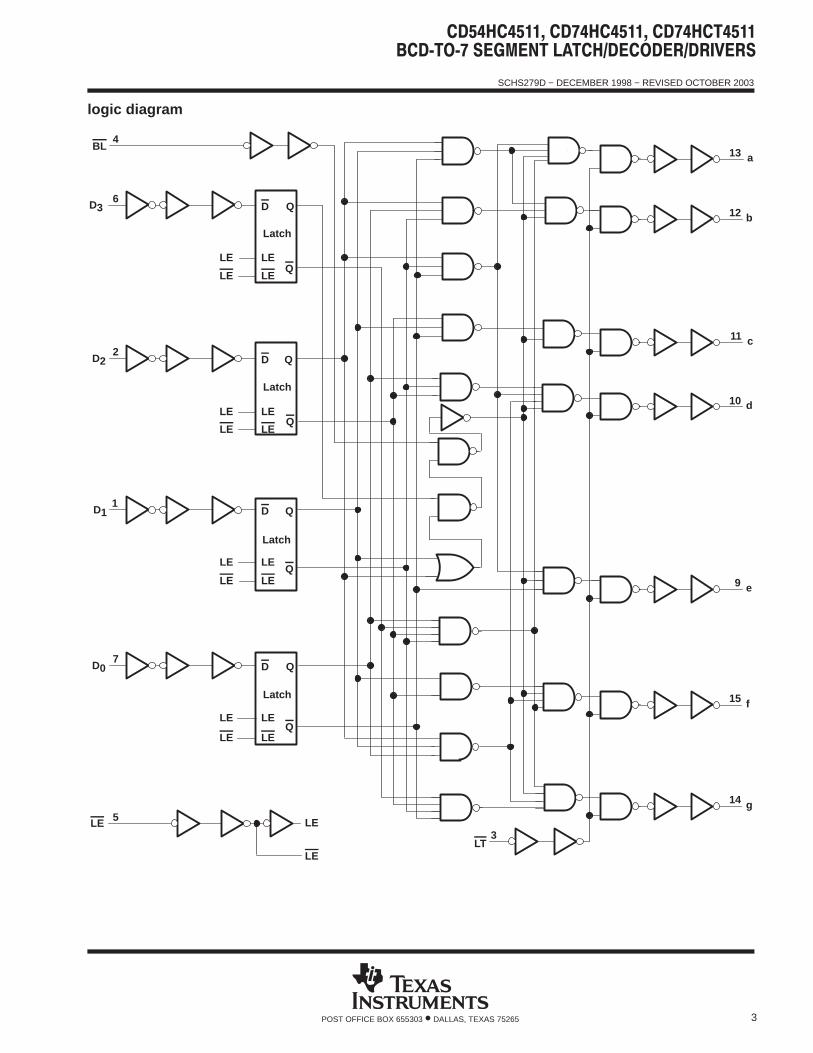
logic diagram
15 f
BL4
6
2
1
7
5
14
9
11
12
13 a
b
c
e
g
3LT
D3
D2
D1
D0
LE
LE
LE
LE
LE
LE
LE
LE
LE
LE
LE
LE
LE
LE
LE
LE
LE
D
D
D
D
Q
Q
Q
Q
Q
Q
Q
Q
Latch
Latch
Latch
Latch
LE
LE
10 d
SCHS279D − DECEMBER 1998 − REVISED OCTOBER 2003
4 POST OFFICE BOX 655303 • DALLAS, TEXAS 75265
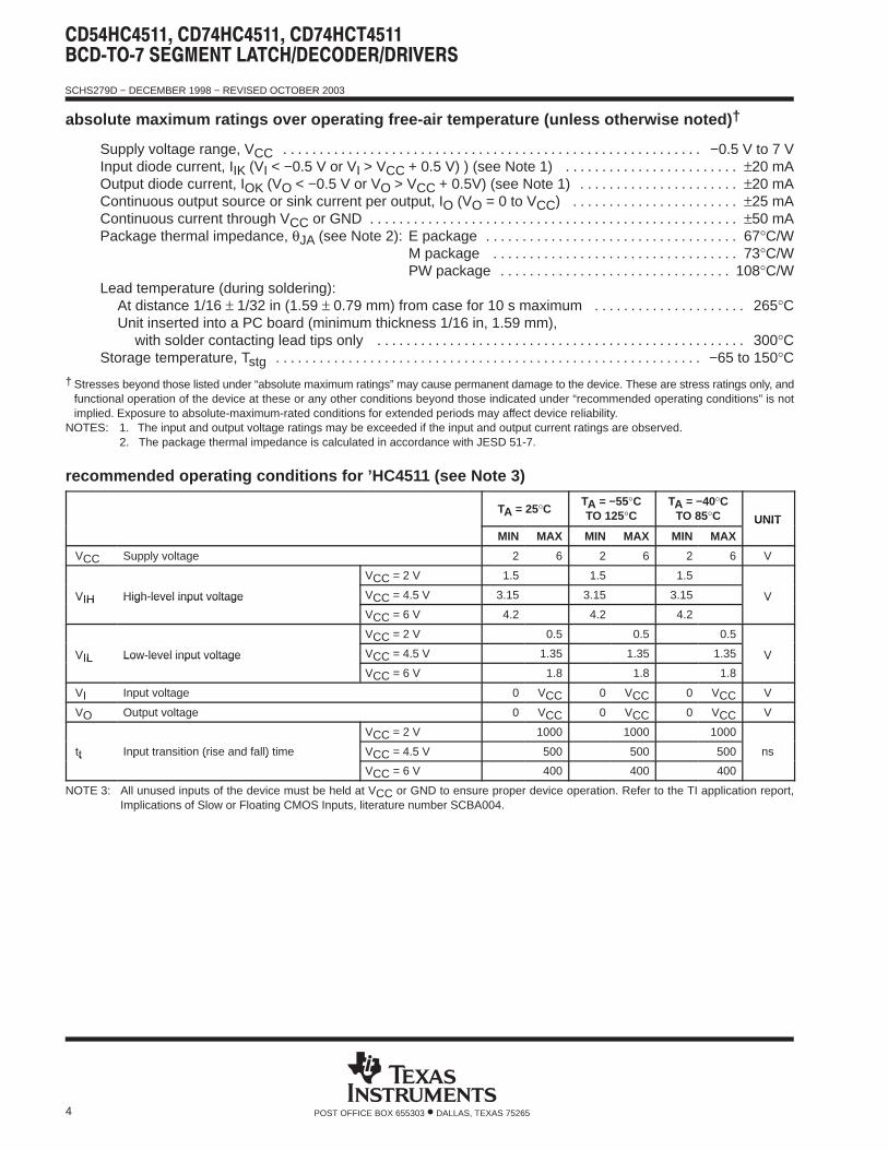
absolute maximum ratings over operating free-air temperature (unless otherwise noted) †
Supply voltage range, VCC −0.5 V to 7 V. . . . . . . . . . . . . . . . . . . . . . . . . . . . . . . . . . . . . . . . . . . . . . . . . . . . . . . . . . Input diode current, IIK (VI < −0.5 V or VI > VCC + 0.5 V) ) (see Note 1) ±20 mA. . . . . . . . . . . . . . . . . . . . . . . . Output diode current, IOK (VO < −0.5 V or VO > VCC + 0.5V) (see Note 1) ±20 mA. . . . . . . . . . . . . . . . . . . . . . Continuous output source or sink current per output, IO (VO = 0 to VCC) ±25 mA. . . . . . . . . . . . . . . . . . . . . . . Continuous current through VCC or GND ±50 mA. . . . . . . . . . . . . . . . . . . . . . . . . . . . . . . . . . . . . . . . . . . . . . . . . . . Package thermal impedance, θJA (see Note 2): E package 67°C/W. . . . . . . . . . . . . . . . . . . . . . . . . . . . . . . . . . .
M package 73°C/W. . . . . . . . . . . . . . . . . . . . . . . . . . . . . . . . . . PW package 108°C/W. . . . . . . . . . . . . . . . . . . . . . . . . . . . . . . .
Lead temperature (during soldering):At distance 1/16 ± 1/32 in (1.59 ± 0.79 mm) from case for 10 s maximum 265°C. . . . . . . . . . . . . . . . . . . . . Unit inserted into a PC board (minimum thickness 1/16 in, 1.59 mm),
with solder contacting lead tips only 300°C. . . . . . . . . . . . . . . . . . . . . . . . . . . . . . . . . . . . . . . . . . . . . . . . . . . Storage temperature, Tstg −65 to 150°C. . . . . . . . . . . . . . . . . . . . . . . . . . . . . . . . . . . . . . . . . . . . . . . . . . . . . . . . . . .
† Stresses beyond those listed under “absolute maximum ratings” may cause permanent damage to the device. These are stress ratings only, andfunctional operation of the device at these or any other conditions beyond those indicated under “recommended operating conditions” is notimplied. Exposure to absolute-maximum-rated conditions for extended periods may affect device reliability.
NOTES: 1. The input and output voltage ratings may be exceeded if the input and output current ratings are observed.2. The package thermal impedance is calculated in accordance with JESD 51-7.
recommended operating conditions for ’HC4511 (see Note 3)
TA = 25°CTA = −55°CTO 125°C
TA = −40°CTO 85°C UNIT
MIN MAX MIN MAX MIN MAXUNIT
VCC Supply voltage 2 6 2 6 2 6 V
VCC = 2 V 1.5 1.5 1.5
VIH High-level input voltage VCC = 4.5 V 3.15 3.15 3.15 VVIH High-level input voltage
VCC = 6 V 4.2 4.2 4.2
V
VCC = 2 V 0.5 0.5 0.5
VIL Low-level input voltage VCC = 4.5 V 1.35 1.35 1.35 VVIL Low-level input voltage
VCC = 6 V 1.8 1.8 1.8
V
VI Input voltage 0 VCC 0 VCC 0 VCC V
VO Output voltage 0 VCC 0 VCC 0 VCC V
VCC = 2 V 1000 1000 1000
tt Input transition (rise and fall) time VCC = 4.5 V 500 500 500 nstt Input transition (rise and fall) time
VCC = 6 V 400 400 400
ns
NOTE 3: All unused inputs of the device must be held at VCC or GND to ensure proper device operation. Refer to the TI application report,Implications of Slow or Floating CMOS Inputs, literature number SCBA004.
SCHS279D − DECEMBER 1998 − REVISED OCTOBER 2003
5POST OFFICE BOX 655303 • DALLAS, TEXAS 75265
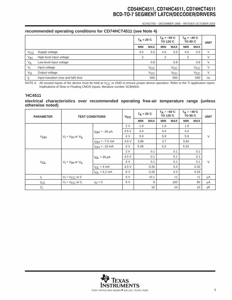
recommended operating conditions for CD74HCT4511 (see Note 4)
TA = 25°CTA = −55°CTO 125°C
TA = −40°CTO 85°C UNIT
MIN MAX MIN MAX MIN MAXUNIT
VCC Supply voltage 4.5 5.5 4.5 5.5 4.5 5.5 V
VIH High-level input voltage 2 2 2 V
VIL Low-level input voltage 0.8 0.8 0.8 V
VI Input voltage VCC VCC VCC V
VO Output voltage VCC VCC VCC V
tt Input transition (rise and fall) time 500 500 500 ns
NOTE 4: All unused inputs of the device must be held at VCC or GND to ensure proper device operation. Refer to the TI application report,Implications of Slow or Floating CMOS Inputs, literature number SCBA004.
’HC4511electrical characteristics over recommended operating free-air temperature range (unlessotherwise noted)
PARAMETER TEST CONDITIONS VCCTA = 25°C
TA = −55°CTO 125°C
TA = −40°CTO 85°C UNITPARAMETER TEST CONDITIONS VCC
MIN MAX MIN MAX MIN MAXUNIT
2 V 1.9 1.9 1.9
IOH = −20 µA 4.5 V 4.4 4.4 4.4
VOH VI = VIH or VIL
IOH = −20 µA
6 V 5.9 5.9 5.9 VVOH VI = VIH or VILIOH = −7.5 mA 4.5 V 3.98 3.7 3.84
V
IOH = −10 mA 6 V 5.48 5.2 5.34
2 V 0.1 0.1 0.1
IOL = 20 µA 4.5 V 0.1 0.1 0.1
VOL VI = VIH or VIL
IOL = 20 µA
6 V 0.1 0.1 0.1 VVOL VI = VIH or VILIOL = 4 mA 4.5 V 0.26 0.4 0.33
V
IOL = 5.2 mA 6 V 0.26 0.4 0.33
II VI = VCC or 0 6 V ±0.1 ±1 ±1 µA
ICC VI = VCC or 0, IO = 0 6 V 8 160 80 µA
Ci 10 10 10 pF
SCHS279D − DECEMBER 1998 − REVISED OCTOBER 2003
6 POST OFFICE BOX 655303 • DALLAS, TEXAS 75265
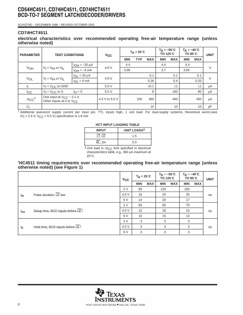
CD74HCT4511electrical characteristics over recommended operating free-air temperature range (unlessotherwise noted)
PARAMETER TEST CONDITIONS VCCTA = 25°C
TA = −55°CTO 125°C
TA = −40°CTO 85°C UNITPARAMETER TEST CONDITIONS VCC
MIN TYP MAX MIN MAX MIN MAXUNIT
VOH VI = VIH or VILIOH = −20 µA
4.5 V4.4 4.4 4.4
VVOH VI = VIH or VIL IOH = −4 mA4.5 V
3.98 3.7 3.84V
VOL VI = VIH or VILIOL = 20 µA
4.5 V0.1 0.1 0.1
VVOL VI = VIH or VIL IOL = 4 mA4.5 V
0.26 0.4 0.33V
II VI = VCC to GND 5.5 V ±0.1 ±1 ±1 µA
ICC VI = VCC or 0, IO = 0 5.5 V 8 160 80 µA
∆ICC† One input at VCC − 2.1 V,Other inputs at 0 or VCC
4.5 V to 5.5 V 100 360 490 450 µA
Ci 10 10 10 pF
† Additional quiescent supply current per input pin, TTL inputs high, 1 unit load. For dual-supply systems, theoretical worst-case(VI = 2.4 V, VCC = 5.5 V) specification is 1.8 mA.
HCT INPUT LOADING TABLE
INPUT UNIT LOADS‡
LT, LE 1.5
BL, Dn 0.3
‡ Unit load is ∆ICC limit specified in electricalcharacteristics table, e.g., 360 µA maximum at25°C.
’HC4511 timing requirements over recommended operating free-air temperature range (unlessotherwise noted) (see Figure 1)
VCCTA = 25°C
TA = −55°CTO 125°C
TA = −40°CTO 85°C UNITVCC
MIN MAX MIN MAX MIN MAXUNIT
2 V 80 120 100
tw Pulse duration, LE low 4.5 V 16 24 20 nstw Pulse duration, LE low
6 V 14 20 17
ns
2 V 60 90 75
tsu Setup time, BCD inputs before LE↑ 4.5 V 12 18 15 nstsu Setup time, BCD inputs before LE↑6 V 10 15 13
ns
2 V 3 3 3
th Hold time, BCD inputs before LE↑ 4.5 V 3 3 3 nsth Hold time, BCD inputs before LE↑6 V 3 3 3
ns
SCHS279D − DECEMBER 1998 − REVISED OCTOBER 2003
7POST OFFICE BOX 655303 • DALLAS, TEXAS 75265
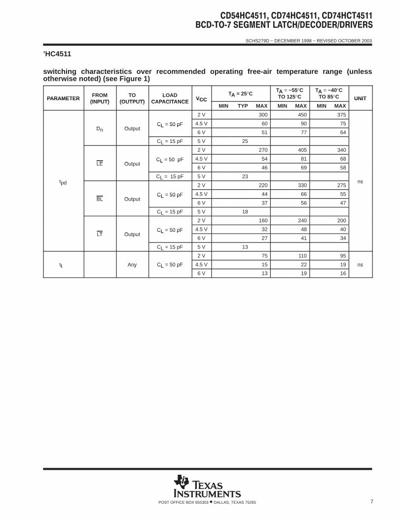
’HC4511
switching characteristics over recommended operating free-air temperature range (unlessotherwise noted) (see Figure 1)
PARAMETERFROM
(INPUT)TO
(OUTPUT)LOAD
CAPACITANCEVCC
TA = 25°CTA = −55°CTO 125°C
TA = −40°CTO 85°C UNITPARAMETER
(INPUT) (OUTPUT) CAPACITANCEVCC
MIN TYP MAX MIN MAX MIN MAXUNIT
2 V 300 450 375
Dn OutputCL = 50 pF 4.5 V 60 90 75
Dn OutputCL = 50 pF
6 V 51 77 64
CL = 15 pF 5 V 25
2 V 270 405 340
LE OutputCL = 50 pF 4.5 V 54 81 68
LE OutputCL = 50 pF
6 V 46 69 58
tpdCL = 15 pF 5 V 23
nstpd 2 V 220 330 275ns
BL OutputCL = 50 pF 4.5 V 44 66 55
BL OutputCL = 50 pF
6 V 37 56 47
CL = 15 pF 5 V 18
2 V 160 240 200
LT OutputCL = 50 pF 4.5 V 32 48 40
LT OutputCL = 50 pF
6 V 27 41 34
CL = 15 pF 5 V 13
2 V 75 110 95
tt Any CL = 50 pF 4.5 V 15 22 19 nstt Any CL = 50 pF
6 V 13 19 16
ns
SCHS279D − DECEMBER 1998 − REVISED OCTOBER 2003
8 POST OFFICE BOX 655303 • DALLAS, TEXAS 75265
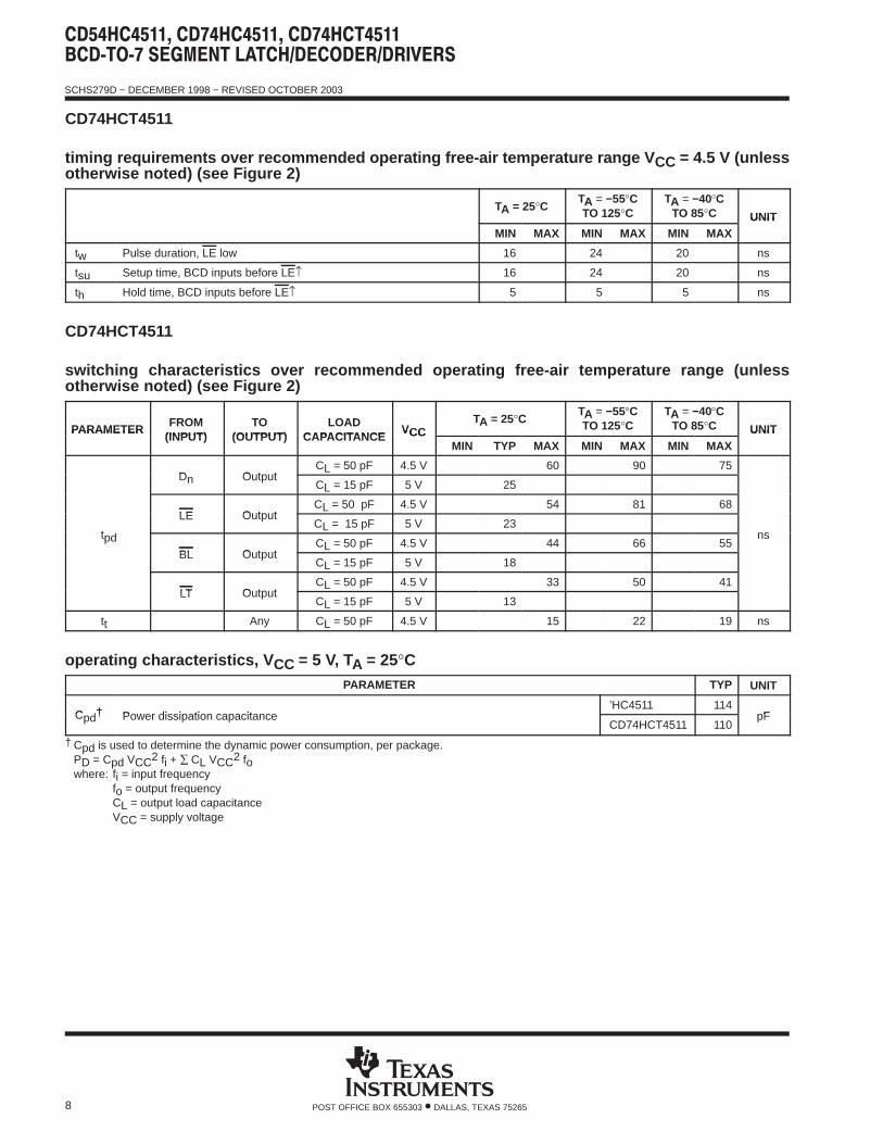
CD74HCT4511
timing requirements over recommended operating free-air temperature range V CC = 4.5 V (unlessotherwise noted) (see Figure 2)
TA = 25°CTA = −55°CTO 125°C
TA = −40°CTO 85°C UNIT
MIN MAX MIN MAX MIN MAXUNIT
tw Pulse duration, LE low 16 24 20 ns
tsu Setup time, BCD inputs before LE↑ 16 24 20 ns
th Hold time, BCD inputs before LE↑ 5 5 5 ns
CD74HCT4511
switching characteristics over recommended operating free-air temperature range (unlessotherwise noted) (see Figure 2)
PARAMETERFROM
(INPUT)TO
(OUTPUT)LOAD
CAPACITANCEVCC
TA = 25°CTA = −55°CTO 125°C
TA = −40°CTO 85°C UNITPARAMETER
(INPUT) (OUTPUT) CAPACITANCEVCC
MIN TYP MAX MIN MAX MIN MAXUNIT
Dn OutputCL = 50 pF 4.5 V 60 90 75
Dn OutputCL = 15 pF 5 V 25
LE OutputCL = 50 pF 4.5 V 54 81 68
tpd
LE OutputCL = 15 pF 5 V 23
nstpd
BL OutputCL = 50 pF 4.5 V 44 66 55
ns
BL OutputCL = 15 pF 5 V 18
LT OutputCL = 50 pF 4.5 V 33 50 41
LT OutputCL = 15 pF 5 V 13
tt Any CL = 50 pF 4.5 V 15 22 19 ns
operating characteristics, V CC = 5 V, TA = 25°CPARAMETER TYP UNIT
Cpd† Power dissipation capacitance’HC4511 114
pFCpd† Power dissipation capacitanceCD74HCT4511 110
pF
† Cpd is used to determine the dynamic power consumption, per package.PD = Cpd VCC2 fi + ∑ CL VCC2 fo where: fi = input frequency
fo = output frequencyCL = output load capacitanceVCC = supply voltage
SCHS279D − DECEMBER 1998 − REVISED OCTOBER 2003
9POST OFFICE BOX 655303 • DALLAS, TEXAS 75265
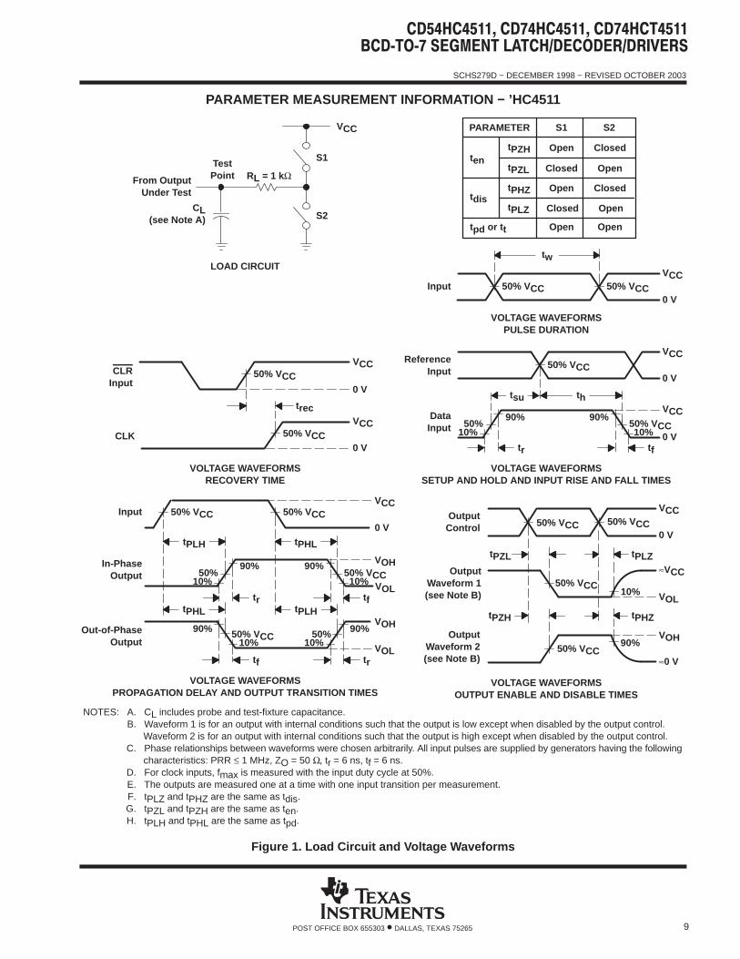
PARAMETER MEASUREMENT INFORMATION − ’HC4511
TestPointFrom Output
Under Test
CL(see Note A)
VCC
S1
S2
LOAD CIRCUIT
PARAMETER
tPZH
tpd or t t
tdis
tentPZL
tPHZ
tPLZ
Open Closed
S1
Closed Open
S2
Open Closed
Closed Open
Open Open
NOTES: A. CL includes probe and test-fixture capacitance.B. Waveform 1 is for an output with internal conditions such that the output is low except when disabled by the output control.
Waveform 2 is for an output with internal conditions such that the output is high except when disabled by the output control.C. Phase relationships between waveforms were chosen arbitrarily. All input pulses are supplied by generators having the following
characteristics: PRR ≤ 1 MHz, ZO = 50 Ω, tr = 6 ns, tf = 6 ns.D. For clock inputs, fmax is measured with the input duty cycle at 50%.E. The outputs are measured one at a time with one input transition per measurement.F. tPLZ and tPHZ are the same as tdis.G. tPZL and tPZH are the same as ten.H. tPLH and tPHL are the same as tpd.
RL = 1 kΩ
VOLTAGE WAVEFORMSSETUP AND HOLD AND INPUT RISE AND FALL TIMES
thtsu
50% VCC
50% VCC50%10%10%
90% 90%
VCC
VCC
0 V
0 V
tr tf
ReferenceInput
DataInput
VOLTAGE WAVEFORMSPROPAGATION DELAY AND OUTPUT TRANSITION TIMES
50% VCC
50% VCC50%10%10%
90% 90%
VCC
VOH
VOL
0 V
tr tf
Input
In-PhaseOutput
50% VCC
tPLH tPHL
50% VCC 50%10% 10%
90%90%VOH
VOLtrtf
tPHL tPLH
Out-of-PhaseOutput
0 V
tw
VOLTAGE WAVEFORMSPULSE DURATION
Input 50% VCC50% VCC
VCC
OutputControl
OutputWaveform 1(see Note B)
OutputWaveform 2(see Note B)
VOL
VOH
tPZL
tPZH
tPLZ
tPHZ
≈VCC
0 V
50% VCC10%
50% VCC≈0 V
VOLTAGE WAVEFORMSOUTPUT ENABLE AND DISABLE TIMES
50% VCC 50% VCC
90%
VCC
VOLTAGE WAVEFORMSRECOVERY TIME
50% VCC
VCC
0 V
CLRInput
CLK 50% VCC
VCC
trec
0 V
Figure 1. Load Circuit and Voltage Waveforms
SCHS279D − DECEMBER 1998 − REVISED OCTOBER 2003
10 POST OFFICE BOX 655303 • DALLAS, TEXAS 75265
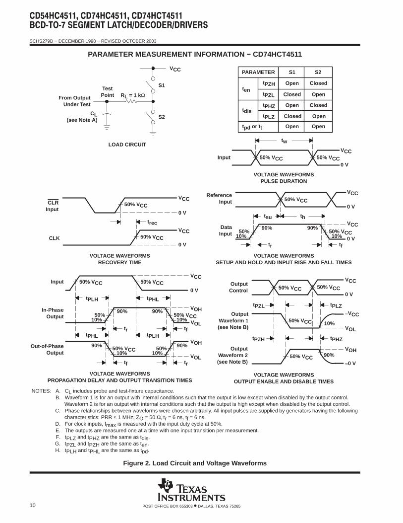
PARAMETER MEASUREMENT INFORMATION − CD74HCT4511
TestPointFrom Output
Under Test
CL(see Note A)
VCC
S1
S2
LOAD CIRCUIT
PARAMETER
tPZH
tpd or t t
tdis
tentPZL
tPHZ
tPLZ
Open Closed
S1
Closed Open
S2
Open Closed
Closed Open
Open Open
NOTES: A. CL includes probe and test-fixture capacitance.B. Waveform 1 is for an output with internal conditions such that the output is low except when disabled by the output control.
Waveform 2 is for an output with internal conditions such that the output is high except when disabled by the output control.C. Phase relationships between waveforms were chosen arbitrarily. All input pulses are supplied by generators having the following
characteristics: PRR ≤ 1 MHz, ZO = 50 Ω, tr = 6 ns, tf = 6 ns.D. For clock inputs, fmax is measured with the input duty cycle at 50%.E. The outputs are measured one at a time with one input transition per measurement.F. tPLZ and tPHZ are the same as tdis.G. tPZL and tPZH are the same as ten.H. tPLH and tPHL are the same as tpd.
RL = 1 kΩ
VOLTAGE WAVEFORMSSETUP AND HOLD AND INPUT RISE AND FALL TIMES
thtsu
50% VCC
50% VCC50%10%10%
90% 90%
VCC
VCC
0 V
0 V
tr tf
ReferenceInput
DataInput
VOLTAGE WAVEFORMSPROPAGATION DELAY AND OUTPUT TRANSITION TIMES
50% VCC
50% VCC50%10%10%
90% 90%
VCC
VOH
VOL
0 V
tr tf
Input
In-PhaseOutput
50% VCC
tPLH tPHL
50% VCC 50%10% 10%
90%90%VOH
VOLtrtf
tPHL tPLH
Out-of-PhaseOutput
0 V
tw
VOLTAGE WAVEFORMSPULSE DURATION
Input 50% VCC50% VCC
VCC
OutputControl
OutputWaveform 1(see Note B)
OutputWaveform 2(see Note B)
VOL
VOH
tPZL
tPZH
tPLZ
tPHZ
≈VCC
0 V
50% VCC 10%
50% VCC≈0 V
VOLTAGE WAVEFORMSOUTPUT ENABLE AND DISABLE TIMES
50% VCC 50% VCC
90%
VCC
VOLTAGE WAVEFORMSRECOVERY TIME
50% VCC
VCC
0 V
CLRInput
CLK 50% VCC
VCC
trec
0 V
Figure 2. Load Circuit and Voltage Waveforms
PACKAGE OPTION ADDENDUM
www.ti.com 10-Jun-2014
Addendum-Page 1
PACKAGING INFORMATION
Orderable Device Status(1)
Package Type PackageDrawing
Pins PackageQty
Eco Plan(2)
Lead/Ball Finish(6)
MSL Peak Temp(3)
Op Temp (°C) Device Marking(4/5)
Samples
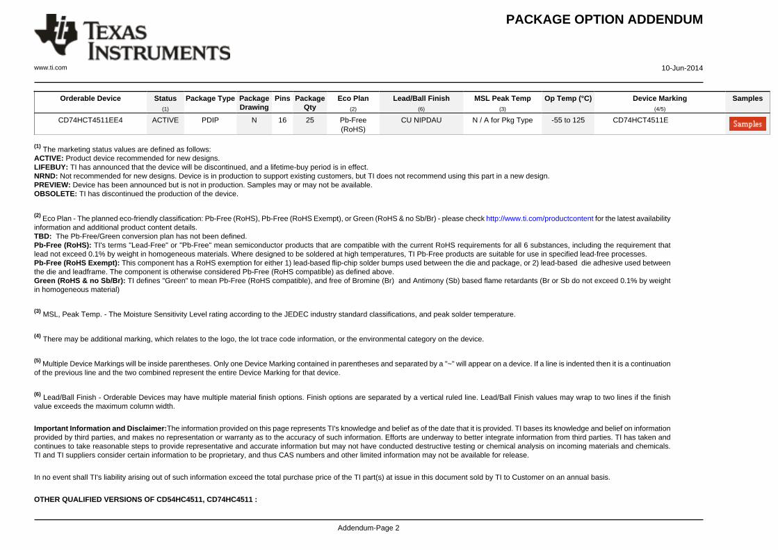
5962-8773301EA ACTIVE CDIP J 16 1 TBD A42 N / A for Pkg Type -55 to 125 5962-8773301EACD54HC4511F3A
CD54HC4511F3A ACTIVE CDIP J 16 1 TBD A42 N / A for Pkg Type -55 to 125 5962-8773301EACD54HC4511F3A
CD74HC4511E ACTIVE PDIP N 16 25 Pb-Free(RoHS)
CU NIPDAU N / A for Pkg Type -55 to 125 CD74HC4511E
CD74HC4511EE4 ACTIVE PDIP N 16 25 Pb-Free(RoHS)
CU NIPDAU N / A for Pkg Type -55 to 125 CD74HC4511E
CD74HC4511M ACTIVE SOIC D 16 40 Green (RoHS& no Sb/Br)
CU NIPDAU Level-1-260C-UNLIM -55 to 125 HC4511M
CD74HC4511M96 ACTIVE SOIC D 16 2500 Green (RoHS& no Sb/Br)
CU NIPDAU Level-1-260C-UNLIM -55 to 125 HC4511M
CD74HC4511M96E4 ACTIVE SOIC D 16 2500 Green (RoHS& no Sb/Br)
CU NIPDAU Level-1-260C-UNLIM -55 to 125 HC4511M
CD74HC4511ME4 ACTIVE SOIC D 16 40 Green (RoHS& no Sb/Br)
CU NIPDAU Level-1-260C-UNLIM -55 to 125 HC4511M
CD74HC4511MG4 ACTIVE SOIC D 16 40 Green (RoHS& no Sb/Br)
CU NIPDAU Level-1-260C-UNLIM -55 to 125 HC4511M
CD74HC4511MT ACTIVE SOIC D 16 250 Green (RoHS& no Sb/Br)
CU NIPDAU Level-1-260C-UNLIM -55 to 125 HC4511M
CD74HC4511PWR ACTIVE TSSOP PW 16 2000 Green (RoHS& no Sb/Br)
CU NIPDAU Level-1-260C-UNLIM -55 to 125 HJ4511
CD74HC4511PWRE4 ACTIVE TSSOP PW 16 2000 Green (RoHS& no Sb/Br)
CU NIPDAU Level-1-260C-UNLIM -55 to 125 HJ4511
CD74HC4511PWRG4 ACTIVE TSSOP PW 16 2000 Green (RoHS& no Sb/Br)
CU NIPDAU Level-1-260C-UNLIM -55 to 125 HJ4511
CD74HC4511PWT ACTIVE TSSOP PW 16 250 Green (RoHS& no Sb/Br)
CU NIPDAU Level-1-260C-UNLIM -55 to 125 HJ4511
CD74HC4511PWTE4 ACTIVE TSSOP PW 16 250 Green (RoHS& no Sb/Br)
CU NIPDAU Level-1-260C-UNLIM -55 to 125 HJ4511
CD74HC4511PWTG4 ACTIVE TSSOP PW 16 250 Green (RoHS& no Sb/Br)
CU NIPDAU Level-1-260C-UNLIM -55 to 125 HJ4511
CD74HCT4511E ACTIVE PDIP N 16 25 Pb-Free(RoHS)
CU NIPDAU N / A for Pkg Type -55 to 125 CD74HCT4511E
PACKAGE OPTION ADDENDUM
www.ti.com 10-Jun-2014
Addendum-Page 2
Orderable Device Status(1)
Package Type PackageDrawing
Pins PackageQty
Eco Plan(2)
Lead/Ball Finish(6)
MSL Peak Temp(3)
Op Temp (°C) Device Marking(4/5)
Samples
CD74HCT4511EE4 ACTIVE PDIP N 16 25 Pb-Free(RoHS)
CU NIPDAU N / A for Pkg Type -55 to 125 CD74HCT4511E
(1) The marketing status values are defined as follows:ACTIVE: Product device recommended for new designs.LIFEBUY: TI has announced that the device will be discontinued, and a lifetime-buy period is in effect.NRND: Not recommended for new designs. Device is in production to support existing customers, but TI does not recommend using this part in a new design.PREVIEW: Device has been announced but is not in production. Samples may or may not be available.OBSOLETE: TI has discontinued the production of the device.
(2) Eco Plan - The planned eco-friendly classification: Pb-Free (RoHS), Pb-Free (RoHS Exempt), or Green (RoHS & no Sb/Br) - please check http://www.ti.com/productcontent for the latest availabilityinformation and additional product content details.TBD: The Pb-Free/Green conversion plan has not been defined.Pb-Free (RoHS): TI's terms "Lead-Free" or "Pb-Free" mean semiconductor products that are compatible with the current RoHS requirements for all 6 substances, including the requirement thatlead not exceed 0.1% by weight in homogeneous materials. Where designed to be soldered at high temperatures, TI Pb-Free products are suitable for use in specified lead-free processes.Pb-Free (RoHS Exempt): This component has a RoHS exemption for either 1) lead-based flip-chip solder bumps used between the die and package, or 2) lead-based die adhesive used betweenthe die and leadframe. The component is otherwise considered Pb-Free (RoHS compatible) as defined above.Green (RoHS & no Sb/Br): TI defines "Green" to mean Pb-Free (RoHS compatible), and free of Bromine (Br) and Antimony (Sb) based flame retardants (Br or Sb do not exceed 0.1% by weightin homogeneous material)
(3) MSL, Peak Temp. - The Moisture Sensitivity Level rating according to the JEDEC industry standard classifications, and peak solder temperature.
(4) There may be additional marking, which relates to the logo, the lot trace code information, or the environmental category on the device.
(5) Multiple Device Markings will be inside parentheses. Only one Device Marking contained in parentheses and separated by a "~" will appear on a device. If a line is indented then it is a continuationof the previous line and the two combined represent the entire Device Marking for that device.
(6) Lead/Ball Finish - Orderable Devices may have multiple material finish options. Finish options are separated by a vertical ruled line. Lead/Ball Finish values may wrap to two lines if the finishvalue exceeds the maximum column width.
Important Information and Disclaimer:The information provided on this page represents TI's knowledge and belief as of the date that it is provided. TI bases its knowledge and belief on informationprovided by third parties, and makes no representation or warranty as to the accuracy of such information. Efforts are underway to better integrate information from third parties. TI has taken andcontinues to take reasonable steps to provide representative and accurate information but may not have conducted destructive testing or chemical analysis on incoming materials and chemicals.TI and TI suppliers consider certain information to be proprietary, and thus CAS numbers and other limited information may not be available for release.
In no event shall TI's liability arising out of such information exceed the total purchase price of the TI part(s) at issue in this document sold by TI to Customer on an annual basis.
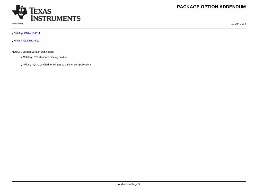
OTHER QUALIFIED VERSIONS OF CD54HC4511, CD74HC4511 :
PACKAGE OPTION ADDENDUM
www.ti.com 10-Jun-2014
Addendum-Page 3
• Catalog: CD74HC4511
• Military: CD54HC4511
NOTE: Qualified Version Definitions:
• Catalog - TI's standard catalog product
• Military - QML certified for Military and Defense Applications
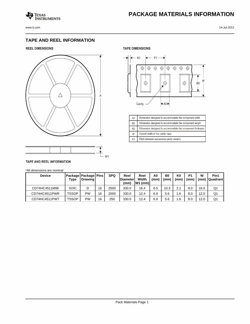
TAPE AND REEL INFORMATION
*All dimensions are nominal
Device PackageType
PackageDrawing
Pins SPQ ReelDiameter
(mm)
ReelWidth
W1 (mm)
A0(mm)
B0(mm)
K0(mm)
P1(mm)
W(mm)
Pin1Quadrant
CD74HC4511M96 SOIC D 16 2500 330.0 16.4 6.5 10.3 2.1 8.0 16.0 Q1
CD74HC4511PWR TSSOP PW 16 2000 330.0 12.4 6.9 5.6 1.6 8.0 12.0 Q1
CD74HC4511PWT TSSOP PW 16 250 330.0 12.4 6.9 5.6 1.6 8.0 12.0 Q1
PACKAGE MATERIALS INFORMATION
www.ti.com 14-Jul-2012
Pack Materials-Page 1
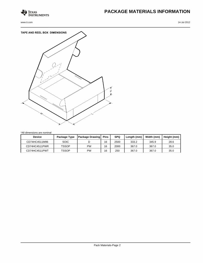
*All dimensions are nominal
Device Package Type Package Drawing Pins SPQ Length (mm) Width (mm) Height (mm)
CD74HC4511M96 SOIC D 16 2500 333.2 345.9 28.6
CD74HC4511PWR TSSOP PW 16 2000 367.0 367.0 35.0
CD74HC4511PWT TSSOP PW 16 250 367.0 367.0 35.0
PACKAGE MATERIALS INFORMATION
www.ti.com 14-Jul-2012
Pack Materials-Page 2
IMPORTANT NOTICE
Texas Instruments Incorporated (TI) reserves the right to make corrections, enhancements, improvements and other changes to itssemiconductor products and services per JESD46, latest issue, and to discontinue any product or service per JESD48, latest issue. Buyersshould obtain the latest relevant information before placing orders and should verify that such information is current and complete.TI’s published terms of sale for semiconductor products (http://www.ti.com/sc/docs/stdterms.htm) apply to the sale of packaged integratedcircuit products that TI has qualified and released to market. Additional terms may apply to the use or sale of other types of TI products andservices.Reproduction of significant portions of TI information in TI data sheets is permissible only if reproduction is without alteration and isaccompanied by all associated warranties, conditions, limitations, and notices. TI is not responsible or liable for such reproduceddocumentation. Information of third parties may be subject to additional restrictions. Resale of TI products or services with statementsdifferent from or beyond the parameters stated by TI for that product or service voids all express and any implied warranties for theassociated TI product or service and is an unfair and deceptive business practice. TI is not responsible or liable for any such statements.Buyers and others who are developing systems that incorporate TI products (collectively, “Designers”) understand and agree that Designersremain responsible for using their independent analysis, evaluation and judgment in designing their applications and that Designers havefull and exclusive responsibility to assure the safety of Designers' applications and compliance of their applications (and of all TI productsused in or for Designers’ applications) with all applicable regulations, laws and other applicable requirements. Designer represents that, withrespect to their applications, Designer has all the necessary expertise to create and implement safeguards that (1) anticipate dangerousconsequences of failures, (2) monitor failures and their consequences, and (3) lessen the likelihood of failures that might cause harm andtake appropriate actions. Designer agrees that prior to using or distributing any applications that include TI products, Designer willthoroughly test such applications and the functionality of such TI products as used in such applications.TI’s provision of technical, application or other design advice, quality characterization, reliability data or other services or information,including, but not limited to, reference designs and materials relating to evaluation modules, (collectively, “TI Resources”) are intended toassist designers who are developing applications that incorporate TI products; by downloading, accessing or using TI Resources in anyway, Designer (individually or, if Designer is acting on behalf of a company, Designer’s company) agrees to use any particular TI Resourcesolely for this purpose and subject to the terms of this Notice.TI’s provision of TI Resources does not expand or otherwise alter TI’s applicable published warranties or warranty disclaimers for TIproducts, and no additional obligations or liabilities arise from TI providing such TI Resources. TI reserves the right to make corrections,enhancements, improvements and other changes to its TI Resources. TI has not conducted any testing other than that specificallydescribed in the published documentation for a particular TI Resource.Designer is authorized to use, copy and modify any individual TI Resource only in connection with the development of applications thatinclude the TI product(s) identified in such TI Resource. NO OTHER LICENSE, EXPRESS OR IMPLIED, BY ESTOPPEL OR OTHERWISETO ANY OTHER TI INTELLECTUAL PROPERTY RIGHT, AND NO LICENSE TO ANY TECHNOLOGY OR INTELLECTUAL PROPERTYRIGHT OF TI OR ANY THIRD PARTY IS GRANTED HEREIN, including but not limited to any patent right, copyright, mask work right, orother intellectual property right relating to any combination, machine, or process in which TI products or services are used. Informationregarding or referencing third-party products or services does not constitute a license to use such products or services, or a warranty orendorsement thereof. Use of TI Resources may require a license from a third party under the patents or other intellectual property of thethird party, or a license from TI under the patents or other intellectual property of TI.TI RESOURCES ARE PROVIDED “AS IS” AND WITH ALL FAULTS. TI DISCLAIMS ALL OTHER WARRANTIES ORREPRESENTATIONS, EXPRESS OR IMPLIED, REGARDING RESOURCES OR USE THEREOF, INCLUDING BUT NOT LIMITED TOACCURACY OR COMPLETENESS, TITLE, ANY EPIDEMIC FAILURE WARRANTY AND ANY IMPLIED WARRANTIES OFMERCHANTABILITY, FITNESS FOR A PARTICULAR PURPOSE, AND NON-INFRINGEMENT OF ANY THIRD PARTY INTELLECTUALPROPERTY RIGHTS. TI SHALL NOT BE LIABLE FOR AND SHALL NOT DEFEND OR INDEMNIFY DESIGNER AGAINST ANY CLAIM,INCLUDING BUT NOT LIMITED TO ANY INFRINGEMENT CLAIM THAT RELATES TO OR IS BASED ON ANY COMBINATION OFPRODUCTS EVEN IF DESCRIBED IN TI RESOURCES OR OTHERWISE. IN NO EVENT SHALL TI BE LIABLE FOR ANY ACTUAL,DIRECT, SPECIAL, COLLATERAL, INDIRECT, PUNITIVE, INCIDENTAL, CONSEQUENTIAL OR EXEMPLARY DAMAGES INCONNECTION WITH OR ARISING OUT OF TI RESOURCES OR USE THEREOF, AND REGARDLESS OF WHETHER TI HAS BEENADVISED OF THE POSSIBILITY OF SUCH DAMAGES.Unless TI has explicitly designated an individual product as meeting the requirements of a particular industry standard (e.g., ISO/TS 16949and ISO 26262), TI is not responsible for any failure to meet such industry standard requirements.Where TI specifically promotes products as facilitating functional safety or as compliant with industry functional safety standards, suchproducts are intended to help enable customers to design and create their own applications that meet applicable functional safety standardsand requirements. Using products in an application does not by itself establish any safety features in the application. Designers mustensure compliance with safety-related requirements and standards applicable to their applications. Designer may not use any TI products inlife-critical medical equipment unless authorized officers of the parties have executed a special contract specifically governing such use.Life-critical medical equipment is medical equipment where failure of such equipment would cause serious bodily injury or death (e.g., lifesupport, pacemakers, defibrillators, heart pumps, neurostimulators, and implantables). Such equipment includes, without limitation, allmedical devices identified by the U.S. Food and Drug Administration as Class III devices and equivalent classifications outside the U.S.TI may expressly designate certain products as completing a particular qualification (e.g., Q100, Military Grade, or Enhanced Product).Designers agree that it has the necessary expertise to select the product with the appropriate qualification designation for their applicationsand that proper product selection is at Designers’ own risk. Designers are solely responsible for compliance with all legal and regulatoryrequirements in connection with such selection.Designer will fully indemnify TI and its representatives against any damages, costs, losses, and/or liabilities arising out of Designer’s non-compliance with the terms and provisions of this Notice.
Mailing Address: Texas Instruments, Post Office Box 655303, Dallas, Texas 75265Copyright © 2017, Texas Instruments Incorporated


![Iƒ{¯fl¤ ¥¢{˙~ƒ ‚h]¯fl¤}ƒ ¥¤pƒ °¡~ · ˘cc†=‘ƒcc£⁄~‚cch ‘cc jƒccfl¤~=i‘‘cc£⁄}¥cc~ ‚xcc˘†cc=‘ƒcc£h‚cc†j˙cc ... ˘†cccc=˙‰cccc](https://img.pdfslide.net/doc/110x75/5b16c8117f8b9a686d8dbb95/if-f-hf-pf-ccfcccch.jpg)