Embed Size (px)
Citation preview

Product
Folder
Sample &Buy
Technical
Documents
Tools &
Software
Support &Community
CC1125SWRS120E –JUNE 2011–REVISED OCTOBER 2014
CC1125 Ultra-High Performance RF Narrowband Transceiver1 Device Overview
1.1 Features1
• High-Performance, Single-Chip Transceiver • Programmable Output Power up to +16 dBm With0.4-dB Step Size– Adjacent Channel Selectivity: 67 dB at
6.25-kHz Offset • Automatic Output Power Ramping– Blocking Performance: 104 dB at 10 MHz • Configurable Data Rates: 0 to 200 kbps– Excellent Receiver Sensitivity • Supported Modulation Formats: 2-FSK,
2-GFSK, 4-FSK, 4-GFSK, MSK, OOK• –129 dBm at 300 bps• WaveMatch: Advanced Digital Signal Processing• –123 dBm at 1.2 kbps
for Improved Sync Detect Performance• –110 dBm at 50 kbps• RoHS-Compliant 5-mm x 5-mm No-Lead QFN– Very Low Phase Noise: –115 dBc/Hz at
32-Pin Package (RHB)10-kHz Offset• Regulations – Suitable for Systems Targeting• Suitable for Systems Targeting ETSI
Compliance WithCategory 1– Europe: ETSI EN 300 220 Category 1, ETSI EN• Separate 128-Byte RX and TX FIFOs
54-25, ETSI EN 300 113, and EN 301 166• Support for Seamless Integration With the CC1190– US: FCC CFR47 Part 15, 24, 90, 101Device for Increased Range Giving up to 3-dB– Japan: ARIB RCR STD-T30, T-67, T-108Improvement in Sensitivity and up to +27-dBm
• Peripherals and Support FunctionsOutput Power– eWOR Functionality for Automatic Low-Power• High Spectral Efficiency (9.6 kbps in 12.5-kHz
Receive PollingChannel in Compliance With FCC NarrowbandingMandate) – Includes Functions for Antenna Diversity
Support• Power Supply– Support for Retransmissions– Wide Supply Voltage Range (2.0 V to 3.6 V)– Support for Auto-Acknowledge of Received– Low Current Consumption:
Packets• RX: 2 mA in RX Sniff Mode– TCXO Support and Control, also in Power• RX: 17 mA Peak Current in Low-Power
ModesMode– Automatic Clear Channel Assessment (CCA) for• RX: 26 mA Peak Current in High-
Listen-Before-Talk (LBT) SystemsPerformance Mode– Built-in Coding Gain Support for Increased• TX: 47 mA at +14 dBm
Range and Robustness– Power Down: 0.12 μA (0.5 μA With Enhanced– Digital RSSI MeasurementWake-On-Radio (eWOR) Timer Running)– Temperature Sensor
1.2 Applications• Social Alarms • IEEE 802.15.4g Systems• Narrowband Ultra-Low-Power Wireless Systems • Home and Building Automation
With Channel Spacing Down to 4 kHz • Wireless Alarm and Security Systems• 169-, 315-, 433-, 868-, 915-, 920-, 950-MHz • Industrial Monitoring and Control
ISM/SRD Band Systems • Wireless Healthcare Applications• Wireless Metering and Wireless Smart Grid (AMR • Wireless Sensor Networks and Active RFID
and AMI)• Private Mobile Radios
1
An IMPORTANT NOTICE at the end of this data sheet addresses availability, warranty, changes, use in safety-critical applications,intellectual property matters and other important disclaimers. PRODUCTION DATA.
CC112X
MARCMain Radio Control UnitUltra low power 16 bit
MCU
256 byteFIFO RAM
buffer
4k byte ROM
RF and DSP frontend
Packet handlerand FIFO control
Configuration andstatus registers
eWOREnhanced ultra low power
Wake On Radio timer
SPI Serial configurationand data interface
Interrupt andIO handler
System bus
PA
LNA_P
LNA_N
90dB dynamic range ADC
90dB dynamic range ADC
High linearityLNA
14dBm highefficiency PA
Cha
nnel
fil
ter
XOSC
Cor
dic
AGCAutomatic Gain Control, 60dB VGA range
RSSI measurements and carrier sense detection
Highly flexible FSK / OOK demodulator
(optional bit clock)
(optional low jitter serial data output for legacy protocols)
Data interface with signal chain access
XOSC_Q1
XOSC_Q2
Ultra low power 32kHz auto-calibrated RC oscillator
(optional 32kHz clock intput)
CSn (chip select)
SI (serial input)
SO (serial output)
SCLK (serial clock)
(optional GPIO0-3)
Mod
ulat
or
Fully integrated Fractional-NFrequency Synthesizer
Output power ramping and OOK / ASK modulation
ifamp
ifamp
(optional autodetectedexternal XOSC / TCXO)
(optional GPIO for antenna diversity)
I
Q
Battery sensor / temp sensor
Power on reset
CC1125SWRS120E –JUNE 2011–REVISED OCTOBER 2014 www.ti.com
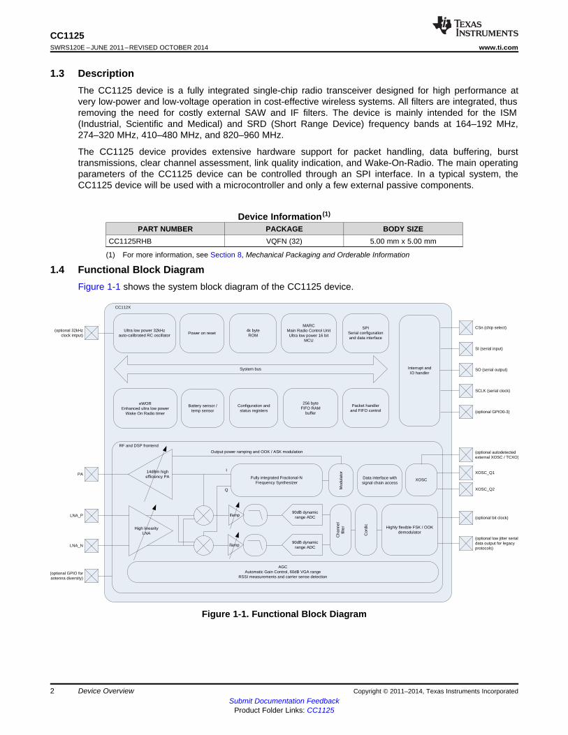
1.3 DescriptionThe CC1125 device is a fully integrated single-chip radio transceiver designed for high performance atvery low-power and low-voltage operation in cost-effective wireless systems. All filters are integrated, thusremoving the need for costly external SAW and IF filters. The device is mainly intended for the ISM(Industrial, Scientific and Medical) and SRD (Short Range Device) frequency bands at 164–192 MHz,274–320 MHz, 410–480 MHz, and 820–960 MHz.
The CC1125 device provides extensive hardware support for packet handling, data buffering, bursttransmissions, clear channel assessment, link quality indication, and Wake-On-Radio. The main operatingparameters of the CC1125 device can be controlled through an SPI interface. In a typical system, theCC1125 device will be used with a microcontroller and only a few external passive components.
Device Information (1)
PART NUMBER PACKAGE BODY SIZECC1125RHB VQFN (32) 5.00 mm x 5.00 mm
(1) For more information, see Section 8, Mechanical Packaging and Orderable Information
1.4 Functional Block DiagramFigure 1-1 shows the system block diagram of the CC1125 device.
Figure 1-1. Functional Block Diagram
2 Device Overview Copyright © 2011–2014, Texas Instruments IncorporatedSubmit Documentation Feedback
Product Folder Links: CC1125
CC1125www.ti.com SWRS120E –JUNE 2011–REVISED OCTOBER 2014
Table of Contents1 Device Overview ......................................... 1 4.15 High-Speed Clock Input (TCXO).................... 19
1.1 Features .............................................. 1 4.16 32-kHz Clock Input .................................. 191.2 Applications........................................... 1 4.17 Low Speed RC Oscillator ........................... 201.3 Description............................................ 2 4.18 I/O and Reset ....................................... 201.4 Functional Block Diagram ............................ 2 4.19 Temperature Sensor ............................... 20
2 Revision History ......................................... 4 4.20 Typical Characteristics .............................. 213 Terminal Configuration and Functions.............. 5 5 Detailed Description ................................... 24
3.1 Pin Diagram .......................................... 5 5.1 Block Diagram....................................... 243.2 Pin Configuration ..................................... 6 5.2 Frequency Synthesizer.............................. 24
4 Specifications ............................................ 7 5.3 Receiver ............................................. 254.1 Absolute Maximum Ratings .......................... 7 5.4 Transmitter .......................................... 254.2 Handling Ratings ..................................... 7 5.5 Radio Control and User Interface ................... 254.3 Recommended Operating Conditions (General 5.6 4.5 Enhanced Wake-On-Radio (eWOR) ............ 25
Characteristics) ....................................... 7 5.7 Sniff Mode........................................... 264.4 Thermal Resistance Characteristics for RHB 5.8 Antenna Diversity ................................... 26
Package .............................................. 75.9 WaveMatch.......................................... 27
4.5 RF Characteristics.................................... 86 Typical Application Circuit ........................... 28
4.6 Regulatory Standards ................................ 87 Device and Documentation Support ............... 29
4.7 Current Consumption, Static Modes ................. 97.1 Device Support ...................................... 29
4.8 Current Consumption, Transmit Modes .............. 97.2 Documentation Support ............................. 30
4.9 Current Consumption, Receive Modes.............. 107.3 Community Resources .............................. 30
4.10 Receive Parameters................................. 117.4 Trademarks.......................................... 30
4.11 Transmit Parameters................................ 177.5 Electrostatic Discharge Caution..................... 30
4.12 PLL Parameters ..................................... 187.6 Glossary ............................................. 30
4.13 Wake-up and Timing ................................ 198 Mechanical Packaging and Orderable
4.14 High-Speed Crystal Oscillator....................... 19 Information .............................................. 31
Copyright © 2011–2014, Texas Instruments Incorporated Table of Contents 3Submit Documentation Feedback
Product Folder Links: CC1125

CC1125SWRS120E –JUNE 2011–REVISED OCTOBER 2014 www.ti.com
2 Revision HistoryNOTE: Page numbers for previous revisions may differ from page numbers in the current version.
This data manual revision history highlights the changes made to the SWRS120D device-specific datamanual to make it an SWRS120E revision.
Changes from Revision D (June 2014) to Revision E Page
• Added Ambient to the temperature range condition and removed Tj from Temperature range ........................... 7• Added data to TCXO table ......................................................................................................... 19
4 Revision History Copyright © 2011–2014, Texas Instruments IncorporatedSubmit Documentation Feedback
Product Folder Links: CC1125
CS
n
SO
(GP
IO1
)
DV
DD
AV
DD
_IF
RB
IAS
AV
DD
_R
F
GP
IO0
RESET_N
GPIO3
GPIO2
DVDD
VDD_GUARD
CC11255
4
3
2
1
LNA_P
LNA_N
DCPL_VCO
AVDD_SYNTH1
TRX_SW
19
20
21
22
23
AV
DD
_P
FD
_C
HP
XO
SC
_Q
2
XO
SC
_Q
1
DC
PL
_P
FD
_C
HP
27
28
29
30
31
DCPL 6
7
PA
18
17
26
25
159 10
11
12
13
14
SI
N.C
.
DC
PL
_X
OS
C
AV
DD
_X
OS
C
8SCLK
16
24E
XT
_X
OS
C3
2
LPF0
LPF1
AV
DD
_S
YN
TH
2
GND
GROUND PAD
CC1125www.ti.com SWRS120E –JUNE 2011–REVISED OCTOBER 2014
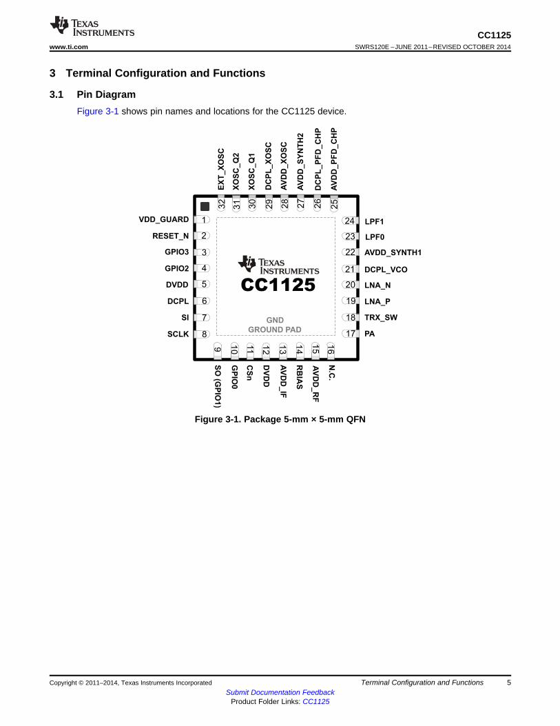
3 Terminal Configuration and Functions
3.1 Pin DiagramFigure 3-1 shows pin names and locations for the CC1125 device.
Figure 3-1. Package 5-mm × 5-mm QFN
Copyright © 2011–2014, Texas Instruments Incorporated Terminal Configuration and Functions 5Submit Documentation Feedback
Product Folder Links: CC1125

CC1125SWRS120E –JUNE 2011–REVISED OCTOBER 2014 www.ti.com
3.2 Pin ConfigurationThe following table lists the pin-out configuration for the CC1125 device.
PIN NO. PIN NAME TYPE / DESCRIPTIONDIRECTION
1 VDD_GUARD Power 2.0–3.6 V VDD2 RESET_N Digital input Asynchronous, active-low digital reset3 GPIO3 Digital I/O General-purpose I/O4 GPIO2 Digital I/O General-purpose I/O5 DVDD Power 2.0–3.6 VDD to internal digital regulator6 DCPL Power Digital regulator output to external decoupling capacitor7 SI Digital input Serial data in8 SCLK Digital input Serial data clock9 SO(GPIO1) Digital I/O Serial data out (general-purpose I/O)10 GPIO0 Digital I/O General-purpose I/O11 CSn Digital input Active-low chip select12 DVDD Power 2.0–3.6 V VDD13 AVDD_IF Power 2.0–3.6 V VDD14 RBIAS Analog External high-precision resistor15 AVDD_RF Power 2.0–3.6 V VDD16 N.C. Not connected17 PA Analog Single-ended TX output (requires DC path to VDD)
TX and RX switch. Connected internally to GND in TX and floating (high-impedance)18 TRX_SW Analog in RX.19 LNA_P Analog Differential RX input (requires DC path to GND)20 LNA_N Analog Differential RX input (requires DC path to GND)21 DCPL_VCO Power Pin for external decoupling of VCO supply regulator22 AVDD_SYNTH1 Power 2.0–3.6 V VDD23 LPF0 Analog External loop filter components24 LPF1 Analog External loop filter components25 AVDD_PFD_CHP Power 2.0–3.6 V VDD26 DCPL_PFD_CHP Power Pin for external decoupling of PFD and CHP regulator27 AVDD_SYNTH2 Power 2.0–3.6 V VDD28 AVDD_XOSC Power 2.0–3.6 V VDD29 DCPL_XOSC Power Pin for external decoupling of XOSC supply regulator
Crystal oscillator pin 1 (must be grounded if a TCXO or other external clock30 XOSC_Q1 Analog connected to EXT_XOSC is used)Crystal oscillator pin 2 (must be left floating if a TCXO or other external clock31 XOSC_Q2 Analog connected to EXT_XOSC is used)Pin for external clock input (must be grounded if a regular crystal connected to32 EXT_XOSC Digital input XOSC_Q1 and XOSC_Q2 is used)
– GND Ground pad The ground pad must be connected to a solid ground plane.
6 Terminal Configuration and Functions Copyright © 2011–2014, Texas Instruments IncorporatedSubmit Documentation Feedback
Product Folder Links: CC1125

CC1125www.ti.com SWRS120E –JUNE 2011–REVISED OCTOBER 2014
4 Specifications
All measurements performed on CC1120EM_868_915 rev.1.0.1, CC1120EM_955 rev.1.2.1,CC1120EM_420_470 rev.1.0.1 or CC1120EM_169 rev.1.2 (fxosc = 32 MHz), and CC1125EM_868_915rev.1.1.0, CC1125EM_420_470 rev.1.1.0, CC1125EM_169 rev.1.1.0, CC1125EM-Cat1-868 (fxosc = 40MHz).
4.1 Absolute Maximum Ratings (1) (2)
PARAMETER MIN MAX UNIT CONDITIONSupply voltage (VDD, AVDD_x) –0.3 3.9 V All supply pins must have the same voltageSolder reflow temperature 260 °C According to IPC/JEDEC J-STD-020Input RF level +10 dBmVoltage on any digital pin –0.3 VDD+0.3 V max 3.9Voltage on analog pins –0.3 2.0 V(including DCPL pins)
(1) Stresses beyond those listed under absolute maximum ratings may cause permanent damage to the device. These are stress ratingsonly, and functional operation of the device at these or any other conditions beyond those indicated under general characteristics is notimplied. Exposure to absolute-maximum-rated conditions for extended periods may affect device reliability.
(2) All voltage values are with respect to VSS, unless otherwise noted.
4.2 Handling RatingsMIN MAX UNIT
Tstg Storage temperature range –40 125 °CHuman body model (HBM), per ANSI/ESDA/JEDEC JS001 (1) –2 2 kVElectrostatic
VESD discharge (ESD) Charged device model (CDM), per JESD22- All pins –500 500 Vperformance: C101 (2)
(1) JEDEC document JEP155 states that 500-V HBM allows safe manufacturing with a standard ESD control process.(2) JEDEC document JEP157 states that 250-V HBM allows safe manufacturing with a standard ESD control process.
4.3 Recommended Operating Conditions (General Characteristics)PARAMETER MIN TYP MAX UNIT CONDITIONVoltage supply range 2.0 3.6 V All supply pins must have the same voltageVoltage on digital inputs 0 VDD VTemperature range –40 85 °C Ambient
4.4 Thermal Resistance Characteristics for RHB Package°C/W (1) AIR FLOW (m/s) (2)
RθJC Junction-to-case (top) 21.1 0.00RθJB Junction-to-board 5.3 0.00RθJA Junction-to-free air 31.3 0.00PsiJT Junction-to-package top 0.2 0.00PsiJB Junction-to-board 5.3 0.00RθJC Junction-to-case (bottom) 0.8 0.00
(1) These values are based on a JEDEC-defined 2S2P system (with the exception of the Theta JC [RΘJC] value, which is based on aJEDEC-defined 1S0P system) and will change based on environment as well as application. For more information, see theseEIA/JEDEC standards:• JESD51-2, Integrated Circuits Thermal Test Method Environmental Conditions - Natural Convection (Still Air)• JESD51-3, Low Effective Thermal Conductivity Test Board for Leaded Surface Mount Packages• JESD51-7, High Effective Thermal Conductivity Test Board for Leaded Surface Mount Packages• JESD51-9, Test Boards for Area Array Surface Mount Package Thermal MeasurementsPower dissipation of 40 mW and an ambient temperature of 25ºC is assumed.
(2) m/s = meters per second
Copyright © 2011–2014, Texas Instruments Incorporated Specifications 7Submit Documentation Feedback
Product Folder Links: CC1125
CC1125SWRS120E –JUNE 2011–REVISED OCTOBER 2014 www.ti.com
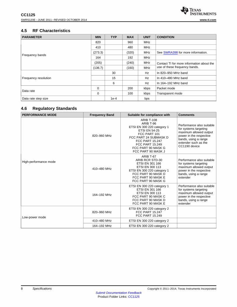
4.5 RF CharacteristicsPARAMETER MIN TYP MAX UNIT CONDITION
820 960 MHz410 480 MHz
(273.3) (320) MHz See SWRA398 for more information.Frequency bands
164 192 MHz(205) (240) MHz Contact TI for more information about the
use of these frequency bands.(136.7) (160) MHz30 Hz In 820–950 MHz band
Frequency resolution 15 Hz In 410–480 MHz band6 Hz In 164–192 MHz band
0 200 kbps Packet modeData rate
0 100 kbps Transparent modeData rate step size 1e-4 bps
4.6 Regulatory StandardsPERFORMANCE MODE Frequency Band Suitable for compliance with Comments
ARIB T-108ARIB T-96 Performance also suitableETSI EN 300 220 category 1 for systems targetingETSI EN 54-25 maximum allowed outputFCC PART 101820–960 MHz power in the respectiveFCC PART 24 SUBMASK D bands, using a rangeFCC PART 15.247 extender such as theFCC PART 15.249 CC1190 deviceFCC PART 90 MASK G
FCC PART 90 MASK JARIB T-67
ARIB RCR STD-30 Performance also suitableHigh-performance mode ETSI EN 301 166 for systems targetingETSI EN 300 113 maximum allowed output410–480 MHz ETSI EN 300 220 category 1 power in the respective
FCC PART 90 MASK D bands, using a rangeFCC PART 90 MASK E extenderFCC PART 90 MASK G
ETSI EN 300 220 category 1 Performance also suitableETSI EN 301 166 for systems targetingETSI EN 300 113 maximum allowed output164–192 MHz FCC PART 90 MASK C power in the respective
FCC PART 90 MASK D bands, using a rangeFCC PART 90 MASK E extender
ETSI EN 300 220 category 2820–960 MHz FCC PART 15.247
FCC PART 15.249Low-power mode410–480 MHz ETSI EN 300 220 category 2164–192 MHz ETSI EN 300 220 category 2
8 Specifications Copyright © 2011–2014, Texas Instruments IncorporatedSubmit Documentation Feedback
Product Folder Links: CC1125

CC1125www.ti.com SWRS120E –JUNE 2011–REVISED OCTOBER 2014
4.7 Current Consumption, Static ModesTA = 25°C, VDD = 3.0 V, fxosc = 32 MHz if nothing else stated.PARAMETER MIN TYP MAX UNIT CONDITION
0.12 1 µAPower down with retention
0.5 µA Low-power RC oscillator runningXOFF mode 170 µA Crystal oscillator / TCXO disabled
Clock running, system waiting with noIDLE mode 1.3 mA radio activity
4.8 Current Consumption, Transmit Modes
4.8.1 950-MHz Band (High-Performance Mode)TA = 25°C, VDD = 3.0 V, fxosc = 32 MHz if nothing else statedPARAMETER MIN TYP MAX UNIT CONDITIONTX current consumption +10 dBm 37 mATX current consumption 0 dBm 26 mA
4.8.2 868-, 915-, and 920-MHz Bands (High-Performance Mode)TA = 25°C, VDD = 3.0 V, fxosc = 40 MHz if nothing else statedPARAMETER MIN TYP MAX UNIT CONDITIONTX current consumption +14 dBm 47 mATX current consumption +10 dBm 38 mA
4.8.3 434-MHz Band (High-Performance Mode)TA = 25°C, VDD = 3.0 V, fxosc = 40 MHz if nothing else statedPARAMETER MIN TYP MAX UNIT CONDITIONTX current consumption +15 dBm 51 mATX current consumption +14 dBm 47 mATX current consumption +10 dBm 36 mA
4.8.4 169-MHz Band (High Performance Mode)TA = 25°C, VDD = 3.0 V, fxosc = 40 MHz if nothing else statedPARAMETER MIN TYP MAX UNIT CONDITIONTX current consumption +15 dBm 56 mATX current consumption +14 dBm 52 mATX current consumption +10 dBm 40 mA
4.8.5 Low-Power ModeTA = 25°C, VDD = 3.0 V, fc = 869.5 MHz, fxosc = 32 MHz if nothing else statedPARAMETER MIN TYP MAX UNIT CONDITIONTX current consumption +10 dBm 32 mA
Copyright © 2011–2014, Texas Instruments Incorporated Specifications 9Submit Documentation Feedback
Product Folder Links: CC1125

CC1125SWRS120E –JUNE 2011–REVISED OCTOBER 2014 www.ti.com
4.9 Current Consumption, Receive Modes
4.9.1 High-Performance ModeTA = 25°C, VDD = 3.0 V, fc = 869.5 MHz, fxosc = 32 MHz if nothing else statedPARAMETER MIN TYP MAX UNIT CONDITIONRX wait for sync Using RX sniff mode, where the receiver1.2 kbps, 4-byte preamble 2 mA wakes up at regular intervals to look for an
incoming packet38.4 kbps, 4-byte preamble 13.4 mARX peak current, fxosc = 40 MHz
Peak current consumption during packet433-, 868-, 915-, and 920-MHz bands 26 mA reception at the sensitivity threshold169-MHz band 27 mAAverage current consumption 50 kbps, 5-byte preamble, 40-kHz RCCheck for data packet every 1 second using 15 µA oscillator used as sleep timerwake on radio
4.9.2 Low-Power ModeTA = 25°C, VDD = 3.0 V, fc = 869.5 MHz, fxosc = 32 MHz if nothing else statedPARAMETER MIN TYP MAX UNIT CONDITIONRX peak current low-power RX mode Peak current consumption during packet17 mA1.2 kbps reception at the sensitivity level
10 Specifications Copyright © 2011–2014, Texas Instruments IncorporatedSubmit Documentation Feedback
Product Folder Links: CC1125

CC1125www.ti.com SWRS120E –JUNE 2011–REVISED OCTOBER 2014
4.10 Receive ParametersAll RX measurements made at the antenna connector, to a bit error rate (BER) limit of 1%.
4.10.1 General Receive Parameters (High-Performance Mode)TA = 25°C, VDD = 3.0 V, fc = 869.5 MHz if nothing else statedPARAMETER MIN TYP MAX UNIT CONDITIONSaturation +10 dBmDigital channel filter programmable bandwidthfxosc = 32 MHz 2.8 200 kHzfxosc = 40 MHz 3.5 250 kHzIIP3, normal mode –14 dBm At maximum gainIIP3, high linearity mode –8 dBm Using 6-dB gain reduction in front end
With carrier sense detection enabled and±12 % assuming 4-byte preambleDatarate offset tolerance±0.2 % With carrier sense detection disabled
Spurious emissionsRadiated emissions measured according to1–13 GHz (VCO leakage at 3.5 GHz) –56 dBm ETSI EN 300 220, fc = 869.5 MHz
30 MHz to 1 GHz < –57 dBmOptimum source impedance868-, 915-, and 920-MHz bands 60 + j60 / 30 + j30 Ω (Differential or single-ended RX
configurations)433-MHz band 100 + j60 / 50+ j30 Ω169-MHz band 140 + j40 / 70 + j20 Ω
Copyright © 2011–2014, Texas Instruments Incorporated Specifications 11Submit Documentation Feedback
Product Folder Links: CC1125

CC1125SWRS120E –JUNE 2011–REVISED OCTOBER 2014 www.ti.com
4.10.2 RX Performance in 950-MHz Band (High-Performance Mode)TA = 25°C, VDD = 3.0 V, fxosc = 32 MHz if nothing else statedPARAMETER MIN TYP MAX UNIT CONDITION
–120 dBm 1.2 kbps, DEV=4 kHz CHF=10 kHz (1)
Sensitivity 50 kbps 2GFSK, DEV=25 kHz, CHF=100–107 dBmNote: Sensitivity can be improved if the TX and kHzRX matching networks are separated. 200 kbps, DEV=83 kHz (outer symbols),–100 dBm CHF=200 kHz, 4GFSK (2)
51 dB ± 12.5 kHz (adjacent channel)52 dB ± 25 kHz (alternate channel)Blocking and Selectivity
1.2 kbps 2-FSK, 12.5-kHz channel separation, 73 dB ± 1 MHz4-kHz deviation, 10-kHz channel filter 76 dB ± 2 MHz
81 dB ± 10 MHz43 dB ± 200 kHz (adjacent channel)
Blocking and Selectivity 51 dB ± 400 kHz (alternate channel)50 kbps 2-GFSK, 200-kHz channel separation,25-kHz deviation, 100-kHz channel filter 62 dB ± 1 MHz(Same modulation format as 802.15.4g 65 dB ± 2 MHzMandatory Mode)
71 dB ± 10 MHz37 dB ± 200 kHz (adjacent channel)44 dB ± 400 kHz (alternate channel)Blocking and Selectivity
200 kbps 4-GFSK, 83-kHz deviation (outer 55 dB ± 1 MHzsymbols), 200-kHz channel filter, zero IF 58 dB ± 2 MHz
64 dB ± 10 MHz
(1) DEV is short for deviation, CHF is short for channel filter bandwidth(2) BT=0.5 is used in all GFSK measurements
12 Specifications Copyright © 2011–2014, Texas Instruments IncorporatedSubmit Documentation Feedback
Product Folder Links: CC1125

CC1125www.ti.com SWRS120E –JUNE 2011–REVISED OCTOBER 2014
4.10.3 RX Performance in 868-, 915-, and 920-MHz Bands (High-Performance Mode)TA = 25°C, VDD = 3.0 V, fxosc = 32 MHz if nothing else stated if nothing else statedPARAMETER MIN TYP MAX UNIT CONDITION
300 bps, DEV=1 kHz CHF=3.8 kHz (1),–129 dBm fxosc = 40 MHz–123 dBm 1.2 kbps, DEV=20 kHz CHF=50 kHz–114 dBm 4.8 kbps OOK
Sensitivity–110 dBm 38.4 kbps, DEV=20 kHz CHF=100 kHz–110 dBm 50 kbps 2GFSK, DEV=25 kHz, CHF=100 kHz
200 kbps, DEV=83 kHz (outer symbols),–103 dBm CHF=200 kHz, 4GFSK62 dB ± 6.25 kHz (adjacent channel)
Blocking and Selectivity 63 dB ± 12.5 kHz (alternate channel)0.3-kbps 2-FSK, 6.25-kHz channelseparation, 1-kHz deviation, 3.8-kHz 83 dB ± 1 MHzchannel filter 87 dB ± 2 MHzfxosc = 40 MHz using TCXO
91 dB ± 10 MHz58 dB + 12.5 kHz (adjacent channel)
Blocking and Selectivity 58 dB ± 25 kHz (alternate channel)1.2-kbps 2-FSK, 12.5-kHz channelseparation, 4-kHz deviation, 10-kHz 78 dB ± 1 MHzchannel filter 82 dB ± 2 MHzfxosc = 40 MHz using TCXO
86 dB ± 10 MHzBlocking and Selectivity 58 dB ± 25 kHz (alternate channel)1.2-kbps 2-GFSK, 25-kHz channel 77 dB ± 1 MHzseparation, 4-kHz deviation, 16-kHz
106 dB ± 2 MHzchannel filterfxosc = 40 MHz using TCXOUsing external SAW filter for 101 dB ± 10 MHzcompliance with ETSI category 1
42 dB ± 100 kHz (adjacent channel)Blocking and Selectivity 43 dB ± 200 kHz (alternate channel)38.4-kbps 2-GFSK, 100-kHz channel 62 dB ± 1 MHzseparation, 20-kHz deviation, 100-
66 dB ± 2 MHzkHz channel filter74 dB ± 10 MHz43 dB ± 200 kHz (adjacent channel)Blocking and Selectivity
50-kbps 2-GFSK, 200-kHz channel 50 dB ± 400 kHz (alternate channel)separation, 25-kHz deviation, 100- 61 dB ± 1 MHzkHz channel filter
65 dB ± 2 MHz(Same modulation format as802.15.4g Mandatory Mode) 74 dB ± 10 MHz
36 dB ± 200 kHz (adjacent channel)Blocking and Selectivity 44 dB ± 400 kHz (alternate channel)200-kbps 4-GFSK, 83-kHz deviation 55 dB ± 1 MHz(outer symbols), 200-kHz channel
59 dB ± 2 MHzfilter, zero IF67 dB ± 10 MHz
Image rejection 1.2 kbps, DEV=4 kHz CHF=10 kHz (1), image at(Image compensation enabled) 58 dB -125 kHzfxosc = 40 MHz using TCXO
(1) DEV is short for deviation, CHF is short for channel filter bandwidth
Copyright © 2011–2014, Texas Instruments Incorporated Specifications 13Submit Documentation Feedback
Product Folder Links: CC1125
CC1125SWRS120E –JUNE 2011–REVISED OCTOBER 2014 www.ti.com
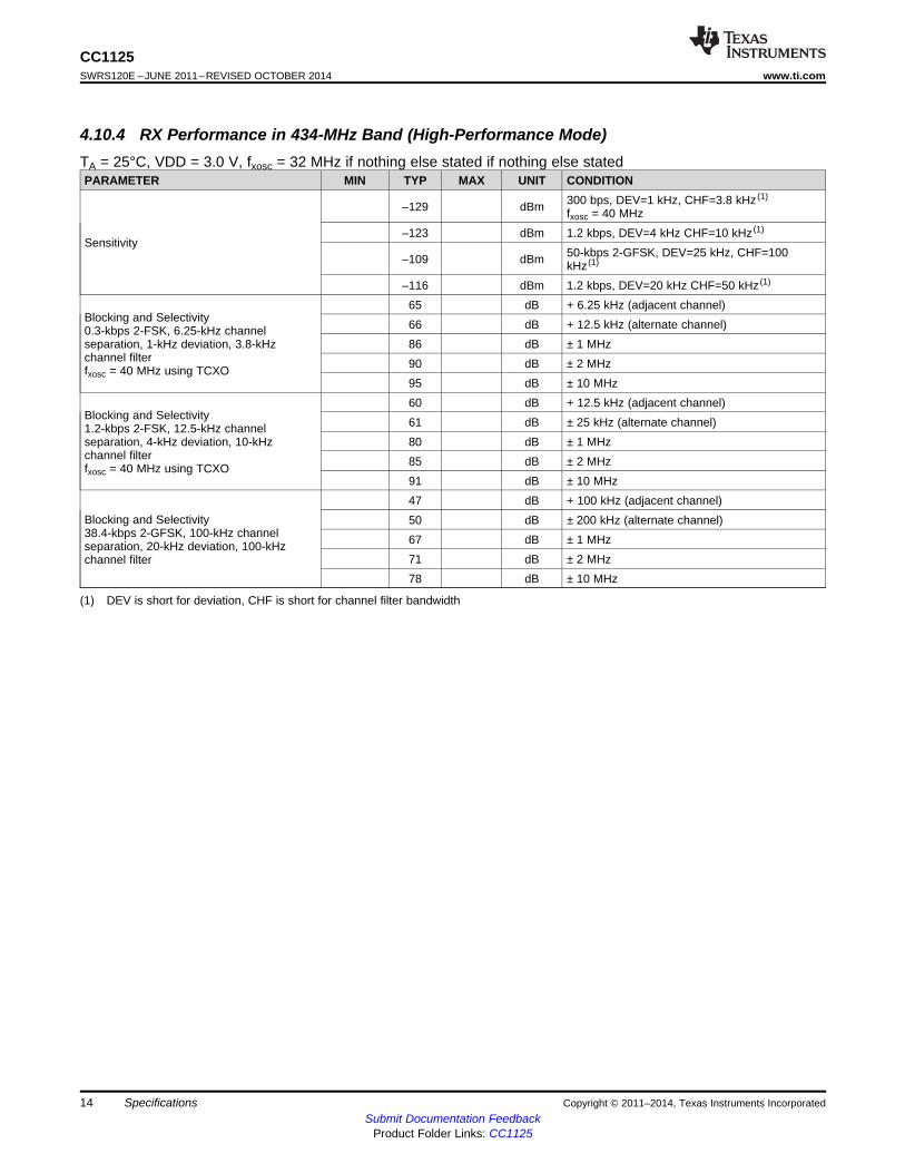
4.10.4 RX Performance in 434-MHz Band (High-Performance Mode)TA = 25°C, VDD = 3.0 V, fxosc = 32 MHz if nothing else stated if nothing else statedPARAMETER MIN TYP MAX UNIT CONDITION
300 bps, DEV=1 kHz, CHF=3.8 kHz (1)–129 dBm fxosc = 40 MHz–123 dBm 1.2 kbps, DEV=4 kHz CHF=10 kHz (1)
Sensitivity50-kbps 2-GFSK, DEV=25 kHz, CHF=100–109 dBm kHz (1)
–116 dBm 1.2 kbps, DEV=20 kHz CHF=50 kHz (1)
65 dB + 6.25 kHz (adjacent channel)Blocking and Selectivity 66 dB + 12.5 kHz (alternate channel)0.3-kbps 2-FSK, 6.25-kHz channelseparation, 1-kHz deviation, 3.8-kHz 86 dB ± 1 MHzchannel filter 90 dB ± 2 MHzfxosc = 40 MHz using TCXO
95 dB ± 10 MHz60 dB + 12.5 kHz (adjacent channel)
Blocking and Selectivity 61 dB ± 25 kHz (alternate channel)1.2-kbps 2-FSK, 12.5-kHz channelseparation, 4-kHz deviation, 10-kHz 80 dB ± 1 MHzchannel filter 85 dB ± 2 MHzfxosc = 40 MHz using TCXO
91 dB ± 10 MHz47 dB + 100 kHz (adjacent channel)
Blocking and Selectivity 50 dB ± 200 kHz (alternate channel)38.4-kbps 2-GFSK, 100-kHz channel 67 dB ± 1 MHzseparation, 20-kHz deviation, 100-kHz
71 dB ± 2 MHzchannel filter78 dB ± 10 MHz
(1) DEV is short for deviation, CHF is short for channel filter bandwidth
14 Specifications Copyright © 2011–2014, Texas Instruments IncorporatedSubmit Documentation Feedback
Product Folder Links: CC1125

CC1125www.ti.com SWRS120E –JUNE 2011–REVISED OCTOBER 2014
4.10.5 RX Performance in 169-MHz Band (High-Performance Mode)TA = 25°C, VDD = 3.0 V, fxosc = 32 MHz if nothing else statedPARAMETER MIN TYP MAX UNIT CONDITION
300 bps, DEV=1 kHz, CHF=3.8 kHz (1)–129 dBm fxosc = 40 MHzSensitivity–123 dBm 1.2 kbps, DEV=4 kHz CHF=10 kHz (1)
67 dB ± 6.25 kHz (adjacent channel)Blocking and Selectivity 67 dB + 12.5 kHz (alternate channel)0.3-kbps 2-FSK, 6.25-kHz channelseparation, 1-kHz deviation, 3.8-kHz 88 dB ± 1 MHzchannel filter 101 dB –2 MHzfxosc = 40 MHz using TCXO
104 dB ± 10 MHz63 dB ± 12.5 kHz (adjacent channel)
Blocking and Selectivity 65 dB ± 25 kHz (alternate channel)1.2-kbps 2-FSK, 12.5-kHz channelseparation, 4-kHz deviation, 10-kHz 82 dB ± 1 MHzchannel filter 86 dB ± 2 MHzfxosc = 40 MHz using TCXO
93 dB –10 MHzSpurious Response Rejection1.2-kbps 2-FSK, 12.5-kHz channel 70 dBseparation, 4-kHz deviation, 10-kHzchannel filterImage Rejection 1.2 kbps, DEV=4 kHz CHF=10 kHz (1), image at66 dB(Image compensation enabled) –125 kHz
(1) DEV is short for deviation, CHF is short for channel filter bandwidth
Copyright © 2011–2014, Texas Instruments Incorporated Specifications 15Submit Documentation Feedback
Product Folder Links: CC1125
CC1125SWRS120E –JUNE 2011–REVISED OCTOBER 2014 www.ti.com
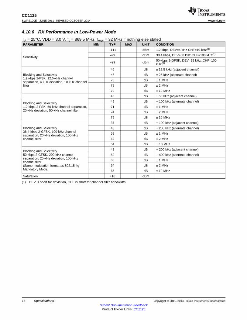
4.10.6 RX Performance in Low-Power ModeTA = 25°C, VDD = 3.0 V, fc = 869.5 MHz, fxosc = 32 MHz if nothing else statedPARAMETER MIN TYP MAX UNIT CONDITION
–111 dBm 1.2 kbps, DEV=4 kHz CHF=10 kHz (1)
–99 dBm 38.4 kbps, DEV=50 kHz CHF=100 kHz (1)Sensitivity
50-kbps 2-GFSK, DEV=25 kHz, CHF=100–99 dBm kHz (1)
46 dB ± 12.5 kHz (adjacent channel)Blocking and Selectivity 46 dB ± 25 kHz (alternate channel)1.2-kbps 2-FSK, 12.5-kHz channel 73 dB ± 1 MHzseparation, 4-kHz deviation, 10-kHz channel
78 dB ± 2 MHzfilter79 dB ± 10 MHz43 dB ± 50 kHz (adjacent channel)45 dB + 100 kHz (alternate channel)Blocking and Selectivity
1.2-kbps 2-FSK, 50-kHz channel separation, 71 dB ± 1 MHz20-kHz deviation, 50-kHz channel filter 74 dB ± 2 MHz
75 dB ± 10 MHz37 dB + 100 kHz (adjacent channel)
Blocking and Selectivity 43 dB + 200 kHz (alternate channel)38.4-kbps 2-GFSK, 100-kHz channel 58 dB ± 1 MHzseparation, 20-kHz deviation, 100-kHz
62 dB ± 2 MHzchannel filter64 dB + 10 MHz43 dB + 200 kHz (adjacent channel)Blocking and Selectivity
50-kbps 2-GFSK, 200-kHz channel 52 dB + 400 kHz (alternate channel)separation, 25-kHz deviation, 100-kHz 60 dB ± 1 MHzchannel filter
64 dB ± 2 MHz(Same modulation format as 802.15.4gMandatory Mode) 65 dB ± 10 MHzSaturation +10 dBm
(1) DEV is short for deviation, CHF is short for channel filter bandwidth
16 Specifications Copyright © 2011–2014, Texas Instruments IncorporatedSubmit Documentation Feedback
Product Folder Links: CC1125

CC1125www.ti.com SWRS120E –JUNE 2011–REVISED OCTOBER 2014
4.11 Transmit ParametersTA = 25°C, VDD = 3.0 V, fc = 869.5 MHz, fxosc = 32 MHz if nothing else statedPARAMETER MIN TYP MAX UNIT CONDITION
+12 dBm At 950 MHz+14 dBm At 915- and 920-MHz+15 dBm At 915- and 920-MHz with VDD = 3.6 V+15 dBm At 868 MHz
Max output power +16 dBm At 868 MHz with VDD = 3.6 V+15 dBm At 433 MHz+16 dBm At 433 MHz with VDD = 3.6 V+15 dBm At 169 MHz+16 dBm At 169 MHz with VDD = 3.6 V–11 dBm Within fine step size range
Min output power–40 dBm Within coarse step size range
Output power step size 0.4 dB Within fine step size range4-GFSK 9.6 kbps in 12.5-kHz channel,
–75 dBc measured in 100-Hz bandwidth at 434 MHz(FCC Part 90 Mask D compliant)4-GFSK 9.6 kbps in 12.5-kHz channel,Adjacent channel power –58 dBc measured in 8.75-kHz bandwidth (ETSI 300 220compliant)2-GFSK 2.4 kbps in 12.5-kHz channel, 1.2-kHz–61 dBc deviation
Spurious emissions <–60 dBm(not including harmonics)HarmonicsSecond Harm, 169 MHz –39 dBmThird Harm, 169 MHz –58 dBmSecond Harm, 433 MHz –56 dBm
Transmission at +14 dBm (or maximum allowedThird Harm, 433 MHz –51 dBm in applicable band where this is less than +14
dBm) using TI reference design.Second Harm, 450 MHz –60 dBmEmissions measured according to ARIB T-96 in
Third Harm, 450 MHz –45 dBm 950-MHz band, ETSI EN 300-220 in 169-, 433-,and 868-MHz bands and FCC part 15.247 inSecond Harm, 868 MHz –40 dBm450- and 915-MHz band.
Third Harm, 868 MHz –42 dBm Fourth harmonic in 915-MHz band will requireextra filtering to meet FCC requirements ifSecond Harm, 915 MHz 56 dBuV/mtransmitting for long intervals (>50-ms periods).
Third Harm, 915 MHz 52 dBuV/mFourth Harm, 915 MHz 60 dBuV/mSecond Harm, 950 MHz –58 dBmThird Harm, 950 MHz –42 dBmOptimum loadImpedance 868-, 915-, and 920-MHz bands 35 + j35 Ω433-MHz band 55 + j25 Ω169-MHz band 80 + j0 Ω
Copyright © 2011–2014, Texas Instruments Incorporated Specifications 17Submit Documentation Feedback
Product Folder Links: CC1125

CC1125SWRS120E –JUNE 2011–REVISED OCTOBER 2014 www.ti.com
4.12 PLL Parameters
4.12.1 High-Performance ModeTA = 25°C, VDD = 3.0 V, fc = 869.5 MHz, fxosc = 40 MHz using TCXO if nothing else statedPARAMETER MIN TYP MAX UNIT CONDITION
–100 dBc/Hz ± 10 kHz offsetPhase noise in 950-MHz band –103 dBc/Hz ± 100 kHz offsetfxosc = 32 MHz
–123 dBc/Hz ± 1 MHz offset–101 dBc/Hz ± 10 kHz offset
Phase noise in 868-, 915-, 920-MHz bands –102 dBc/Hz ± 100 kHz offset–124 dBc/Hz ± 1 MHz offset–107 dBc/Hz ± 10 kHz offset
Phase noise in 433-MHz band –110 dBc/Hz ± 100 kHz offset–130 dBc/Hz ± 1 MHz offset–115 dBc/Hz ± 10 kHz offset
Phase noise in 169-MHz band –115 dBc/Hz ± 100 kHz offset–135 dBc/Hz ± 1 MHz offset
4.12.2 Low-Power ModeTA = 25°C, VDD = 3.0 V, fc = 869.5 MHz, fxosc = 32 MHz if nothing else statedPARAMETER MIN TYP MAX UNIT CONDITION
–90 dBc/Hz ± 10 kHz offsetPhase noise in 950-MHz band –92 dBc/Hz ± 100 kHz offset
–124 dBc/Hz ± 1 MHz offset–95 dBc/Hz ± 10 kHz offset
Phase noise in 868-, 915- , and 920-MHz –95 dBc/Hz ± 100 kHz offsetbands–124 dBc/Hz ± 1 MHz offset–98 dBc/Hz ± 10 kHz offset
Phase noise in 433-MHz band –102 dBc/Hz ± 100 kHz offset–129 dBc/Hz ± 1 MHz offset–106 dBc/Hz ± 10 kHz offset
Phase noise in 169-MHz band –110 dBc/Hz ± 100 kHz offset–136 dBc/Hz ± 1 MHz offset
18 Specifications Copyright © 2011–2014, Texas Instruments IncorporatedSubmit Documentation Feedback
Product Folder Links: CC1125
CC1125www.ti.com SWRS120E –JUNE 2011–REVISED OCTOBER 2014
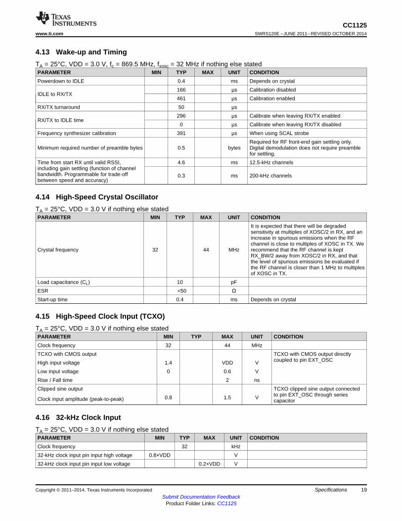
4.13 Wake-up and TimingTA = 25°C, VDD = 3.0 V, fc = 869.5 MHz, fxosc = 32 MHz if nothing else statedPARAMETER MIN TYP MAX UNIT CONDITIONPowerdown to IDLE 0.4 ms Depends on crystal
166 µs Calibration disabledIDLE to RX/TX
461 µs Calibration enabledRX/TX turnaround 50 µs
296 µs Calibrate when leaving RX/TX enabledRX/TX to IDLE time
0 µs Calibrate when leaving RX/TX disabledFrequency synthesizer calibration 391 µs When using SCAL strobe
Required for RF front-end gain settling only.Minimum required number of preamble bytes 0.5 bytes Digital demodulation does not require preamble
for settling.Time from start RX until valid RSSI, 4.6 ms 12.5-kHz channelsincluding gain settling (function of channelbandwidth. Programmable for trade-off 0.3 ms 200-kHz channelsbetween speed and accuracy)
4.14 High-Speed Crystal OscillatorTA = 25°C, VDD = 3.0 V if nothing else statedPARAMETER MIN TYP MAX UNIT CONDITION
It is expected that there will be degradedsensitivity at multiples of XOSC/2 in RX, and anincrease in spurious emissions when the RFchannel is close to multiples of XOSC in TX. We
Crystal frequency 32 44 MHz recommend that the RF channel is keptRX_BW/2 away from XOSC/2 in RX, and thatthe level of spurious emissions be evaluated ifthe RF channel is closer than 1 MHz to multiplesof XOSC in TX.
Load capacitance (CL) 10 pFESR <50 ΩStart-up time 0.4 ms Depends on crystal
4.15 High-Speed Clock Input (TCXO)TA = 25°C, VDD = 3.0 V if nothing else statedPARAMETER MIN TYP MAX UNIT CONDITIONClock frequency 32 44 MHzTCXO with CMOS output TCXO with CMOS output directly
coupled to pin EXT_OSCHigh input voltage 1.4 VDD VLow input voltage 0 0.6 VRise / Fall time 2 nsClipped sine output TCXO clipped sine output connected
to pin EXT_OSC through series0.8 1.5 VClock input amplitude (peak-to-peak) capacitor
4.16 32-kHz Clock InputTA = 25°C, VDD = 3.0 V if nothing else statedPARAMETER MIN TYP MAX UNIT CONDITIONClock frequency 32 kHz32-kHz clock input pin input high voltage 0.8×VDD V32-kHz clock input pin input low voltage 0.2×VDD V
Copyright © 2011–2014, Texas Instruments Incorporated Specifications 19Submit Documentation Feedback
Product Folder Links: CC1125

CC1125SWRS120E –JUNE 2011–REVISED OCTOBER 2014 www.ti.com
4.17 Low Speed RC OscillatorTA = 25°C, VDD = 3.0 V if nothing else statedPARAMETER MIN TYP MAX UNIT CONDITION
After calibration (calibrated against the high-Frequency 32/40 kHz speed XOSC)Relative to frequency reference (for example,Frequency accuracy after calibration ±0.1 % 32-MHz crystal or TCXO)
Initial calibration time 1.6 ms
4.18 I/O and ResetTA = 25°C, VDD = 3.0 V if nothing else statedPARAMETER MIN TYP MAX UNIT CONDITIONLogic input high voltage 0.8×VDD VLogic input low voltage 0.2×VDD VLogic output high voltage 0.8×VDD V
At 4-mA output load or lessLogic output low voltage 0.2×VDD VPower-on reset threshold 1.3 V Voltage on DVDD pin
4.19 Temperature SensorTA = 25°C, VDD = 3.0 V if nothing else statedPARAMETER MIN TYP MAX UNIT CONDITIONTemperature sensor range –40 85 °C
Change in sensor output voltage versusTemperature coefficient 2.66 mV / °C change in temperatureTypical sensor output voltage at TA = 25°C,Typical output voltage 794 mV VDD = 3.0 VChange in sensor output voltage versusVDD coefficient 1.17 mV / V change in VDD
The CC1125 device can be configured to provide a voltage proportional to temperature on GPIO1. Thetemperature can be estimated by measuring this voltage (see Section 4.19, Temperature Sensor). For moreinformation, see the temperature sensor design note (SWRA415).
20 Specifications Copyright © 2011–2014, Texas Instruments IncorporatedSubmit Documentation Feedback
Product Folder Links: CC1125
0
10
20
30
40
50
60
70
80
90
860 862 864 866 868 870 872 874 876 878
Frequency (MHz)
Sele
ctivity (
dB
)
0
10
20
30
40
50
60
70
80
90
868.6 868.8 869 869.2 869.4 869.6 869.8 870
Frequency (MHz)
Sele
ctivity (
dB
)
20.8
21.2
21.6
22
22.4
22.8
23.2
-130 -80 -30 20
Input Level (dBm)
RX
Cu
rren
t(m
A)
-130
-128
-126
-124
-122
-120
-118
-116
-114
3 5 7 9 11 13 15 17
Sync Word Detect Threshold
Sen
sitiv
ity (
dB
m)
-125
-124
-123
-122
-121
-120
-40 0 40 80
Temperature (ºC)
Sen
sitiv
ity (
dB
m)
-124
-123
-122
-121
-120
2 2.5 3 3.5
Supply Voltage (V)
Sen
sitiv
ity (
dB
m)
CC1125www.ti.com SWRS120E –JUNE 2011–REVISED OCTOBER 2014
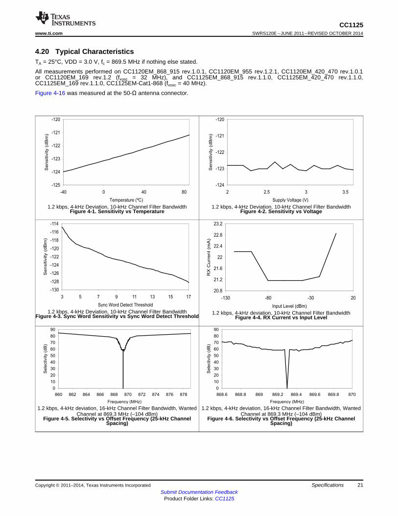
4.20 Typical CharacteristicsTA = 25°C, VDD = 3.0 V, fc = 869.5 MHz if nothing else stated.
All measurements performed on CC1120EM_868_915 rev.1.0.1, CC1120EM_955 rev.1.2.1, CC1120EM_420_470 rev.1.0.1or CC1120EM_169 rev.1.2 (fxosc = 32 MHz), and CC1125EM_868_915 rev.1.1.0, CC1125EM_420_470 rev.1.1.0,CC1125EM_169 rev.1.1.0, CC1125EM-Cat1-868 (fxosc = 40 MHz).
Figure 4-16 was measured at the 50-Ω antenna connector.
1.2 kbps, 4-kHz Deviation, 10-kHz Channel Filter Bandwidth 1.2 kbps, 4-kHz Deviation, 10-kHz Channel Filter BandwidthFigure 4-1. Sensitivity vs Temperature Figure 4-2. Sensitivity vs Voltage
1.2 kbps, 4-kHz Deviation, 10-kHz Channel Filter Bandwidth 1.2 kbps, 4-kHz deviation, 10-kHz Channel Filter BandwidthFigure 4-3. Sync Word Sensitivity vs Sync Word Detect Threshold Figure 4-4. RX Current vs Input Level
1.2 kbps, 4-kHz deviation, 16-kHz Channel Filter Bandwidth, Wanted 1.2 kbps, 4-kHz deviation, 16-kHz Channel Filter Bandwidth, WantedChannel at 869.3 MHz (–104 dBm) Channel at 869.3 MHz (–104 dBm)
Figure 4-5. Selectivity vs Offset Frequency (25-kHz Channel Figure 4-6. Selectivity vs Offset Frequency (25-kHz ChannelSpacing) Spacing)
Copyright © 2011–2014, Texas Instruments Incorporated Specifications 21Submit Documentation Feedback
Product Folder Links: CC1125

15
15.5
16
16.5
17
-40 0 40 80
Temperature (ºC)
Ou
tpu
tP
ow
er
(dB
m)
0
10
20
30
40
50
60
7F 7B 77 73 6F 6B 67 63 5F 5B 57 53 4F 4B 47 43
PA power setting
TX
Cu
rre
nt(m
A)
-50
-40
-30
-20
-10
0
10
20
7F 7B 77 73 6F 6B 67 63 5F 5B 57 53 4F 4B 47 43
PA power setting
Ou
tpu
t P
ow
er
(dB
m)
6
8
10
12
14
16
18
2 2.5 3 3.5
Supply Voltage (V)
Ou
tpu
tP
ow
er
(dB
m)
0
10
20
30
40
50
60
70
869.05 869.1 869.15 869.2 869.25 869.3 869.35
Frequency (MHz)
Sele
ctivity (
dB
)
iqic enabled
iqic disabled
-40
-20
0
20
40
60
80
100
-150 -100 -50 0
Input Level (dBm)
RS
SI
CC1125SWRS120E –JUNE 2011–REVISED OCTOBER 2014 www.ti.com
Typical Characteristics (continued)
Figure 4-7. RSSI vs Input Level Figure 4-8. Automatic Image Cancellation
Figure 4-9. Output Power vs VoltageMax Setting, 170 MHz Figure 4-10. Output Power at 868 MHz
vs PA Power Setting
Figure 4-11. TX Current at 868 MHz Figure 4-12. Output Power vs Temperaturevs PA Power Setting Max Setting, 170 MHz, 3.6 V
22 Specifications Copyright © 2011–2014, Texas Instruments IncorporatedSubmit Documentation Feedback
Product Folder Links: CC1125

1.5
1.7
1.9
2.1
2.3
2.5
2.7
2.9
3.1
0 5 10 15 20 25 30 35
Current (mA)
GP
IOO
utp
utH
igh
Vo
lta
ge
(V)
0
200
400
600
800
1000
1200
1400
0 5 10 15 20 25 30 35
Current (mA)
GP
IOO
utp
utL
ow
Vo
lta
ge
(mV
)
CC1125www.ti.com SWRS120E –JUNE 2011–REVISED OCTOBER 2014
Typical Characteristics (continued)
1.2 kbps 2-FSK, DEV = 4 kHz200 kbps, DEV = 83 kHz (Outer Symbols), 4GFSK Figure 4-14. Eye DiagramFigure 4-13. Eye Diagram
9.6 kbps in 12.5 kHz ChannelFigure 4-15. FCC Part 90 Mask D Figure 4-16. Output Power vs Load Impedance (+14-dBm Setting)
Figure 4-18. GPIO Output Low Voltage vs Current Being SinkedFigure 4-17. GPIO Output High Voltage vs Current Being Sourced
Copyright © 2011–2014, Texas Instruments Incorporated Specifications 23Submit Documentation Feedback
Product Folder Links: CC1125

CC112X
MARCMain Radio Control UnitUltra low power 16 bit
MCU
256 byteFIFO RAM
buffer
4k byte ROM
RF and DSP frontend
Packet handlerand FIFO control
Configuration andstatus registers
eWOREnhanced ultra low power
Wake On Radio timer
SPI Serial configurationand data interface
Interrupt andIO handler
System bus
PA
LNA_P
LNA_N
90dB dynamic range ADC
90dB dynamic range ADC
High linearityLNA
14dBm highefficiency PA
Cha
nnel
fil
ter
XOSC
Cor
dic
AGCAutomatic Gain Control, 60dB VGA range
RSSI measurements and carrier sense detection
Highly flexible FSK / OOK demodulator
(optional bit clock)
(optional low jitter serial data output for legacy protocols)
Data interface with signal chain access
XOSC_Q1
XOSC_Q2
Ultra low power 32kHz auto-calibrated RC oscillator
(optional 32kHz clock intput)
CSn (chip select)
SI (serial input)
SO (serial output)
SCLK (serial clock)
(optional GPIO0-3)
Mod
ulat
or
Fully integrated Fractional-NFrequency Synthesizer
Output power ramping and OOK / ASK modulation
ifamp
ifamp
(optional autodetectedexternal XOSC / TCXO)
(optional GPIO for antenna diversity)
I
Q
Battery sensor / temp sensor
Power on reset
CC1125SWRS120E –JUNE 2011–REVISED OCTOBER 2014 www.ti.com
5 Detailed Description
5.1 Block DiagramFigure 5-1 shows the system block diagram of the CC1125 device.
Figure 5-1. System Block Diagram
5.2 Frequency SynthesizerAt the center of the CC1125 device there is a fully integrated, fractional-N, ultra-high-performancefrequency synthesizer. The frequency synthesizer is designed for excellent phase noise performance,providing very high selectivity and blocking performance. The system is designed to comply with the moststringent regulatory spectral masks at maximum transmit power.
Either a crystal can be connected to XOSC_Q1 and XOSC_Q2, or a TCXO can be connected to theEXT_XOSC input. The oscillator generates the reference frequency for the synthesizer, as well as clocksfor the analog-to-digital converter (ADC) and the digital part. To reduce system cost, CC1125 device hashigh-accuracy frequency estimation and compensation registers to measure and compensate for crystalinaccuracies. This compensation enables the use of lower cost crystals. If a TCXO is used, the CC1125device automatically turns on and off the TCXO when needed to support low-power modes and Wake-On-Radio operation.
24 Detailed Description Copyright © 2011–2014, Texas Instruments IncorporatedSubmit Documentation Feedback
Product Folder Links: CC1125

CC1125www.ti.com SWRS120E –JUNE 2011–REVISED OCTOBER 2014
5.3 ReceiverThe CC1125 device features a highly flexible receiver. The received RF signal is amplified by the low-noise amplifier (LNA) and is down-converted in quadrature (I/Q) to the intermediate frequency (IF). At IF,the I/Q signals are digitized by the high dynamic-range ADCs.
An advanced automatic gain control (AGC) unit adjusts the front-end gain, and enables the CC1125device to receive strong and weak signals, even in the presence of strong interferers. High-attenuationchannels and data filtering enable reception with strong neighbor channel interferers. The I/Q signal isconverted to a phase and magnitude signal to support the FSK and OOK modulation schemes.
NOTEA unique I/Q compensation algorithm removes any problem of I/Q mismatch, thus avoidingtime-consuming and costly I/Q image calibration steps.
5.4 TransmitterThe CC1125 transmitter is based on direct synthesis of the RF frequency (in-loop modulation). To use thespectrum effectively, the CC1125 device has extensive data filtering and shaping in TX mode to supporthigh throughput data communication in narrowband channels. The modulator also controls power rampingto remove issues such as spectral splattering when driving external high-power RF amplifiers.
5.5 Radio Control and User InterfaceThe CC1125 digital control system is built around the main radio control (MARC), which is implementedusing an internal high-performance, 16-bit ultra-low-power processor. MARC handles power modes, radiosequencing, and protocol timing.
A 4-wire SPI serial interface is used for configuration and data buffer access. The digital basebandincludes support for channel configuration, packet handling, and data buffering. The host MCU can stay inpower-down mode until a valid RF packet is received. This greatly reduces power consumption. When thehost MCU receives a valid RF packet, it burst-reads the data. This reduces the required computing power.
The CC1125 radio control and user interface are based on the widely used CC1101 transceiver. Thisrelationship enables an easy transition between the two platforms. The command strobes and the mainradio states are the same for the two platforms.
For legacy formats, the CC1125 device also supports two serial modes.• Synchronous serial mode: The CC1125 device performs bit synchronization and provides the MCU
with a bit clock with associated data.• Transparent mode: The CC1125 device outputs the digital baseband signal using a digital interpolation
filter to eliminate jitter introduced by digital filtering and demodulation.
5.6 4.5 Enhanced Wake-On-Radio (eWOR)eWOR, using a flexible integrated sleep timer, enables automatic receiver polling with no intervention fromthe MCU. When the CC1125 device enters RX mode, it listens and then returns to sleep if a valid RFpacket is not received. The sleep interval and duty cycle can be configured to make a trade-off betweennetwork latency and power consumption. Incoming messages are time-stamped to simplify timer re-synchronization.
The eWOR timer runs off an ultra-low-power 32-kHz RC oscillator. To improve timing accuracy, the RCoscillator can be automatically calibrated to the RF crystal in configurable intervals.
Copyright © 2011–2014, Texas Instruments Incorporated Detailed Description 25Submit Documentation Feedback
Product Folder Links: CC1125

CC1125SWRS120E –JUNE 2011–REVISED OCTOBER 2014 www.ti.com
5.7 Sniff ModeThe CC1125 device supports quick start up times, and requires few preamble bits. Sniff mode uses theseconditions to dramatically reduce the current consumption while the receiver is waiting for data.
Because the CC1125 device can wake up and settle much faster than the duration of most preambles, itis not required to be in RX mode continuously while waiting for a packet to arrive. Instead, the enhancedWake-On-Radio feature can be used to put the device into sleep mode periodically. By setting anappropriate sleep time, the CC1125 device can wake up and receive the packet when it arrives with noperformance loss. This sequence removes the need for accurate timing synchronization betweentransmitter and receiver, and lets the user trade off current consumption between the transmitter andreceiver.
For more information, see the sniff mode design note (SWRA428).
5.8 Antenna DiversityAntenna diversity can increase performance in a multipath environment. An external antenna switch isrequired. The CC1201 device uses one of the GPIO pins to automatically control the switch. This devicealso supports differential output control signals typically used in RF switches.
If antenna diversity is enabled, the GPIO alternates between high and low states until a valid RF inputsignal is detected. An optional acknowledge packet can be transmitted without changing the state of theGPIO.
An incoming RF signal can be validated by received signal strength or by using the automatic preambledetector. Using the automatic preamble detector ensures a more robust system and avoids the need toset a defined signal strength threshold (such a threshold sets the sensitivity limit of the system).
26 Detailed Description Copyright © 2011–2014, Texas Instruments IncorporatedSubmit Documentation Feedback
Product Folder Links: CC1125
CC1125www.ti.com SWRS120E –JUNE 2011–REVISED OCTOBER 2014
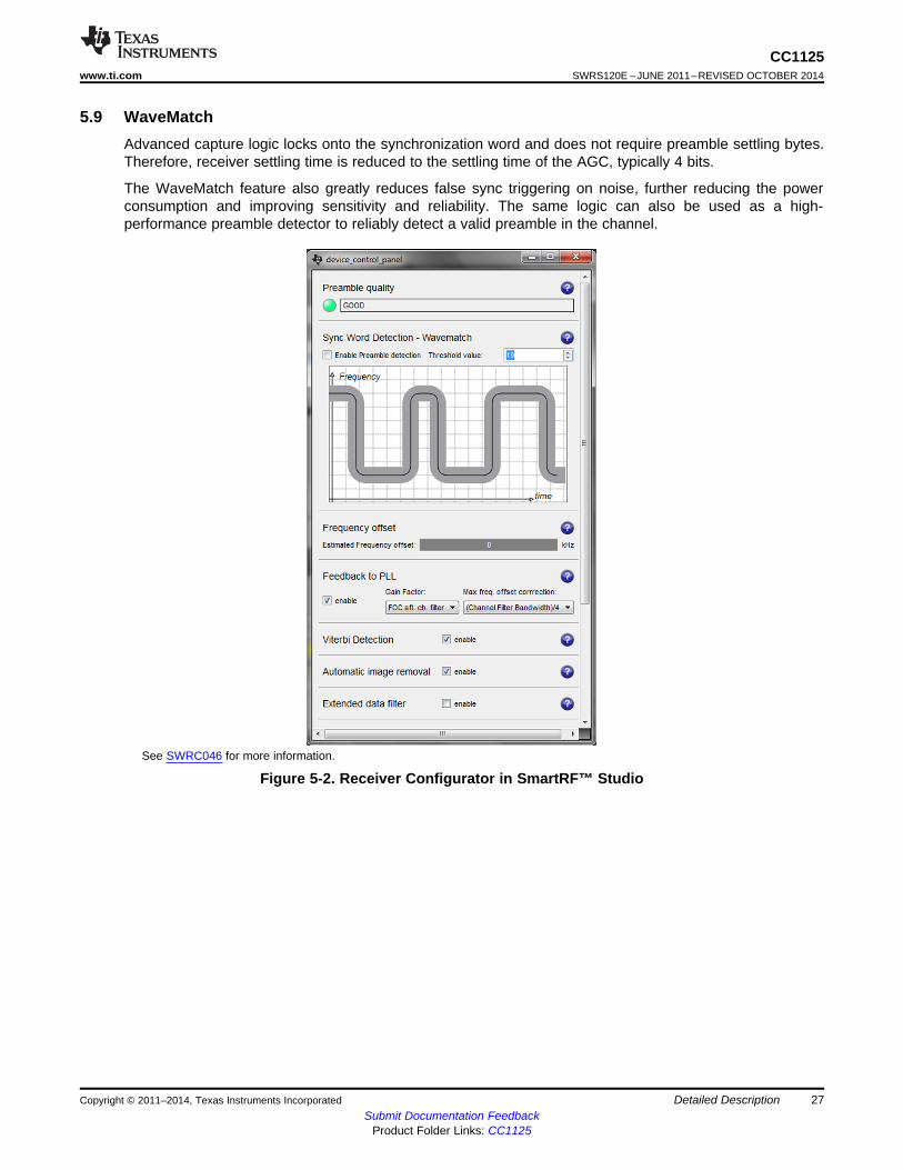
5.9 WaveMatchAdvanced capture logic locks onto the synchronization word and does not require preamble settling bytes.Therefore, receiver settling time is reduced to the settling time of the AGC, typically 4 bits.
The WaveMatch feature also greatly reduces false sync triggering on noise, further reducing the powerconsumption and improving sensitivity and reliability. The same logic can also be used as a high-performance preamble detector to reliably detect a valid preamble in the channel.
See SWRC046 for more information.
Figure 5-2. Receiver Configurator in SmartRF™ Studio
Copyright © 2011–2014, Texas Instruments Incorporated Detailed Description 27Submit Documentation Feedback
Product Folder Links: CC1125

vddext_vdd in out
TPS799xx
Optional Voltage Regulator
for supply noise isolation
(optional control pin
from CC1125)A
VD
D_P
FD
_C
HP
XO
SC
_Q
2
XO
SC
_Q
1
DC
PL
_P
FD
_C
HP
AV
DD
_S
YN
TH
2
DC
PL
_X
OS
C
AV
DD
_X
OS
C
EX
T_X
OS
C
RESET_N
GPIO3
GPIO2
DVDD
VDD_GUARD
DCPL
SI
SCLK
CS
n
SO
(G
PIO
1)
DV
DD
RB
IAS
AV
DD
_IF
AV
DD
_R
F
N.C
.
GP
IO0
LNA_P
LNA_N
DCPL_VCO
AVDD_SYNTH1
PA
TRX_SW
LPF0
LPF1vdd
vd
d
vd
d
vdd
vd
d
CC11255
4
3
2
1
6
7
8
13
12
11
109
14
15
16
20
21
22
23
24
19
18
17
28
29
30
31
32
27
26
25
vdd
40 MHz
crystal
Optional
XOSC/
TCXO
MCU connection
SPI interface and
optional gpio pins
vd
d
vd
d
vd
d
vd
d
CC1125SWRS120E –JUNE 2011–REVISED OCTOBER 2014 www.ti.com
6 Typical Application Circuit
NOTEThis section is intended only as an introduction.
Very few external components are required for the operation of the CC1125 device. Figure 6-1 shows atypical application circuit. The board layout will greatly influence the RF performance of the CC1125device. Figure 6-1 does not show decoupling capacitors for power pins.
Figure 6-1. Typical Application Circuit
For more information, see the reference designs available for the CC1125 device in Section 7.2,Documentation Support.
28 Typical Application Circuit Copyright © 2011–2014, Texas Instruments IncorporatedSubmit Documentation Feedback
Product Folder Links: CC1125
CC1125www.ti.com SWRS120E –JUNE 2011–REVISED OCTOBER 2014
7 Device and Documentation Support
7.1 Device Support
7.1.1 Development Support
7.1.1.1 Configuration Software
The CC1125 device can be configured using the SmartRF Studio software (SWRC046). The SmartRFStudio software is highly recommended for obtaining optimum register settings, and for evaluatingperformance and functionality.
7.1.2 Device and Development-Support Tool NomenclatureTo designate the stages in the product development cycle, TI assigns prefixes to the part numbers of allmicroprocessors (MPUs) and support tools. Each device has one of three prefixes: X, P, or null (no prefix)(for example, CC1125). Texas Instruments recommends two of three possible prefix designators for itssupport tools: TMDX and TMDS. These prefixes represent evolutionary stages of product developmentfrom engineering prototypes (TMDX) through fully qualified production devices and tools (TMDS).
Device development evolutionary flow:
X Experimental device that is not necessarily representative of the final device's electricalspecifications and may not use production assembly flow.
P Prototype device that is not necessarily the final silicon die and may not necessarily meetfinal electrical specifications.
null Production version of the silicon die that is fully qualified.
Support tool development evolutionary flow:
TMDX Development-support product that has not yet completed Texas Instruments internalqualification testing.
TMDS Fully qualified development-support product.
X and P devices and TMDX development-support tools are shipped against the following disclaimer:
"Developmental product is intended for internal evaluation purposes."
Production devices and TMDS development-support tools have been characterized fully, and the qualityand reliability of the device have been demonstrated fully. TI's standard warranty applies.
Predictions show that prototype devices (X or P) have a greater failure rate than the standard productiondevices. Texas Instruments recommends that these devices not be used in any production systembecause their expected end-use failure rate still is undefined. Only qualified production devices are to beused.
TI device nomenclature also includes a suffix with the device family name. This suffix indicates thepackage type (for example, RHB), the temperature range (for example, blank is the default commercialtemperature range), and the device speed range, in megahertz. provides a legend for reading thecomplete device name for any CC1125 device.
For orderable part numbers of CC1125 devices in the QFN package types, see the Package OptionAddendum of this document, the TI website (www.ti.com), or contact your TI sales representative.
Copyright © 2011–2014, Texas Instruments Incorporated Device and Documentation Support 29Submit Documentation Feedback
Product Folder Links: CC1125
CC1125SWRS120E –JUNE 2011–REVISED OCTOBER 2014 www.ti.com
7.2 Documentation SupportThe following documents supplement the CC1125 processor. Copies of these documents are available onthe Internet at www.ti.com. Tip: Enter the literature number in the search box provided at www.ti.com.
SWRR106 CC112x IPC 868- and 915-MHz 2-layer Reference Design
SWRR107 CC112x IPC 868- and 915-MHz 4-layer Reference Design
SWRR100 CC1125EM 169-MHz Reference Design
SWRR101 CC1125EM 420- to 470-MHz Reference Design
SWRR102 CC1121EM 868- to 915-MHz Reference Design
SWRR097 CC1120EM CAT1 868-MHz Reference Design
SWRC046 SmartRF Studio Software
SWRA428 CC112x/CC120x Sniff Mode Application Note
7.3 Community ResourcesThe following links connect to TI community resources. Linked contents are provided "AS IS" by therespective contributors. They do not constitute TI specifications and do not necessarily reflect TI's views;see TI's Terms of Use.
TI E2E™ Online Community TI's Engineer-to-Engineer (E2E) Community. Created to fostercollaboration among engineers. At e2e.ti.com, you can ask questions, share knowledge,explore ideas and help solve problems with fellow engineers.
TI Embedded Processors Wiki Texas Instruments Embedded Processors Wiki. Established to helpdevelopers get started with Embedded Processors from Texas Instruments and to fosterinnovation and growth of general knowledge about the hardware and software surroundingthese devices.
7.4 TrademarksSmartRF, E2E are trademarks of Texas Instruments.
7.5 Electrostatic Discharge CautionThis integrated circuit can be damaged by ESD. Texas Instruments recommends that all integrated circuits be handled withappropriate precautions. Failure to observe proper handling and installation procedures can cause damage.
ESD damage can range from subtle performance degradation to complete device failure. Precision integrated circuits may be moresusceptible to damage because very small parametric changes could cause the device not to meet its published specifications.
7.6 GlossarySLYZ022 — TI Glossary.
This glossary lists and explains terms, acronyms, and definitions.
30 Device and Documentation Support Copyright © 2011–2014, Texas Instruments IncorporatedSubmit Documentation Feedback
Product Folder Links: CC1125

CC1125www.ti.com SWRS120E –JUNE 2011–REVISED OCTOBER 2014
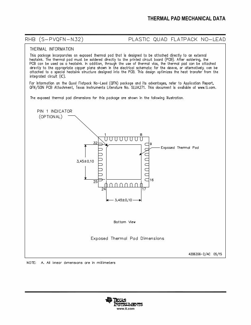
8 Mechanical Packaging and Orderable Information
The following pages include mechanical packaging and orderable information. This information is the mostcurrent data available for the designated devices. This data is subject to change without notice andrevision of this document. For browser-based versions of this data sheet, refer to the left-hand navigation.
Copyright © 2011–2014, Texas Instruments Incorporated Mechanical Packaging and Orderable Information 31Submit Documentation Feedback
Product Folder Links: CC1125
PACKAGE OPTION ADDENDUM
www.ti.com 28-Mar-2018
Addendum-Page 1
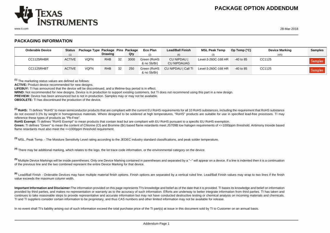
PACKAGING INFORMATION
Orderable Device Status(1)
Package Type PackageDrawing
Pins PackageQty
Eco Plan(2)
Lead/Ball Finish(6)
MSL Peak Temp(3)
Op Temp (°C) Device Marking(4/5)
Samples
CC1125RHBR ACTIVE VQFN RHB 32 3000 Green (RoHS& no Sb/Br)
CU NIPDAU |CU NIPDAUAG
Level-3-260C-168 HR -40 to 85 CC1125
CC1125RHBT ACTIVE VQFN RHB 32 250 Green (RoHS& no Sb/Br)
CU NIPDAU | Call TI Level-3-260C-168 HR -40 to 85 CC1125
(1) The marketing status values are defined as follows:ACTIVE: Product device recommended for new designs.LIFEBUY: TI has announced that the device will be discontinued, and a lifetime-buy period is in effect.NRND: Not recommended for new designs. Device is in production to support existing customers, but TI does not recommend using this part in a new design.PREVIEW: Device has been announced but is not in production. Samples may or may not be available.OBSOLETE: TI has discontinued the production of the device.
(2) RoHS: TI defines "RoHS" to mean semiconductor products that are compliant with the current EU RoHS requirements for all 10 RoHS substances, including the requirement that RoHS substancedo not exceed 0.1% by weight in homogeneous materials. Where designed to be soldered at high temperatures, "RoHS" products are suitable for use in specified lead-free processes. TI mayreference these types of products as "Pb-Free".RoHS Exempt: TI defines "RoHS Exempt" to mean products that contain lead but are compliant with EU RoHS pursuant to a specific EU RoHS exemption.Green: TI defines "Green" to mean the content of Chlorine (Cl) and Bromine (Br) based flame retardants meet JS709B low halogen requirements of <=1000ppm threshold. Antimony trioxide basedflame retardants must also meet the <=1000ppm threshold requirement.
(3) MSL, Peak Temp. - The Moisture Sensitivity Level rating according to the JEDEC industry standard classifications, and peak solder temperature.
(4) There may be additional marking, which relates to the logo, the lot trace code information, or the environmental category on the device.
(5) Multiple Device Markings will be inside parentheses. Only one Device Marking contained in parentheses and separated by a "~" will appear on a device. If a line is indented then it is a continuationof the previous line and the two combined represent the entire Device Marking for that device.
(6) Lead/Ball Finish - Orderable Devices may have multiple material finish options. Finish options are separated by a vertical ruled line. Lead/Ball Finish values may wrap to two lines if the finishvalue exceeds the maximum column width.
Important Information and Disclaimer:The information provided on this page represents TI's knowledge and belief as of the date that it is provided. TI bases its knowledge and belief on informationprovided by third parties, and makes no representation or warranty as to the accuracy of such information. Efforts are underway to better integrate information from third parties. TI has taken andcontinues to take reasonable steps to provide representative and accurate information but may not have conducted destructive testing or chemical analysis on incoming materials and chemicals.TI and TI suppliers consider certain information to be proprietary, and thus CAS numbers and other limited information may not be available for release.
In no event shall TI's liability arising out of such information exceed the total purchase price of the TI part(s) at issue in this document sold by TI to Customer on an annual basis.

PACKAGE OPTION ADDENDUM
www.ti.com 28-Mar-2018
Addendum-Page 2


IMPORTANT NOTICE
Texas Instruments Incorporated (TI) reserves the right to make corrections, enhancements, improvements and other changes to itssemiconductor products and services per JESD46, latest issue, and to discontinue any product or service per JESD48, latest issue. Buyersshould obtain the latest relevant information before placing orders and should verify that such information is current and complete.TI’s published terms of sale for semiconductor products (http://www.ti.com/sc/docs/stdterms.htm) apply to the sale of packaged integratedcircuit products that TI has qualified and released to market. Additional terms may apply to the use or sale of other types of TI products andservices.Reproduction of significant portions of TI information in TI data sheets is permissible only if reproduction is without alteration and isaccompanied by all associated warranties, conditions, limitations, and notices. TI is not responsible or liable for such reproduceddocumentation. Information of third parties may be subject to additional restrictions. Resale of TI products or services with statementsdifferent from or beyond the parameters stated by TI for that product or service voids all express and any implied warranties for theassociated TI product or service and is an unfair and deceptive business practice. TI is not responsible or liable for any such statements.Buyers and others who are developing systems that incorporate TI products (collectively, “Designers”) understand and agree that Designersremain responsible for using their independent analysis, evaluation and judgment in designing their applications and that Designers havefull and exclusive responsibility to assure the safety of Designers' applications and compliance of their applications (and of all TI productsused in or for Designers’ applications) with all applicable regulations, laws and other applicable requirements. Designer represents that, withrespect to their applications, Designer has all the necessary expertise to create and implement safeguards that (1) anticipate dangerousconsequences of failures, (2) monitor failures and their consequences, and (3) lessen the likelihood of failures that might cause harm andtake appropriate actions. Designer agrees that prior to using or distributing any applications that include TI products, Designer willthoroughly test such applications and the functionality of such TI products as used in such applications.TI’s provision of technical, application or other design advice, quality characterization, reliability data or other services or information,including, but not limited to, reference designs and materials relating to evaluation modules, (collectively, “TI Resources”) are intended toassist designers who are developing applications that incorporate TI products; by downloading, accessing or using TI Resources in anyway, Designer (individually or, if Designer is acting on behalf of a company, Designer’s company) agrees to use any particular TI Resourcesolely for this purpose and subject to the terms of this Notice.TI’s provision of TI Resources does not expand or otherwise alter TI’s applicable published warranties or warranty disclaimers for TIproducts, and no additional obligations or liabilities arise from TI providing such TI Resources. TI reserves the right to make corrections,enhancements, improvements and other changes to its TI Resources. TI has not conducted any testing other than that specificallydescribed in the published documentation for a particular TI Resource.Designer is authorized to use, copy and modify any individual TI Resource only in connection with the development of applications thatinclude the TI product(s) identified in such TI Resource. NO OTHER LICENSE, EXPRESS OR IMPLIED, BY ESTOPPEL OR OTHERWISETO ANY OTHER TI INTELLECTUAL PROPERTY RIGHT, AND NO LICENSE TO ANY TECHNOLOGY OR INTELLECTUAL PROPERTYRIGHT OF TI OR ANY THIRD PARTY IS GRANTED HEREIN, including but not limited to any patent right, copyright, mask work right, orother intellectual property right relating to any combination, machine, or process in which TI products or services are used. Informationregarding or referencing third-party products or services does not constitute a license to use such products or services, or a warranty orendorsement thereof. Use of TI Resources may require a license from a third party under the patents or other intellectual property of thethird party, or a license from TI under the patents or other intellectual property of TI.TI RESOURCES ARE PROVIDED “AS IS” AND WITH ALL FAULTS. TI DISCLAIMS ALL OTHER WARRANTIES ORREPRESENTATIONS, EXPRESS OR IMPLIED, REGARDING RESOURCES OR USE THEREOF, INCLUDING BUT NOT LIMITED TOACCURACY OR COMPLETENESS, TITLE, ANY EPIDEMIC FAILURE WARRANTY AND ANY IMPLIED WARRANTIES OFMERCHANTABILITY, FITNESS FOR A PARTICULAR PURPOSE, AND NON-INFRINGEMENT OF ANY THIRD PARTY INTELLECTUALPROPERTY RIGHTS. TI SHALL NOT BE LIABLE FOR AND SHALL NOT DEFEND OR INDEMNIFY DESIGNER AGAINST ANY CLAIM,INCLUDING BUT NOT LIMITED TO ANY INFRINGEMENT CLAIM THAT RELATES TO OR IS BASED ON ANY COMBINATION OFPRODUCTS EVEN IF DESCRIBED IN TI RESOURCES OR OTHERWISE. IN NO EVENT SHALL TI BE LIABLE FOR ANY ACTUAL,DIRECT, SPECIAL, COLLATERAL, INDIRECT, PUNITIVE, INCIDENTAL, CONSEQUENTIAL OR EXEMPLARY DAMAGES INCONNECTION WITH OR ARISING OUT OF TI RESOURCES OR USE THEREOF, AND REGARDLESS OF WHETHER TI HAS BEENADVISED OF THE POSSIBILITY OF SUCH DAMAGES.Unless TI has explicitly designated an individual product as meeting the requirements of a particular industry standard (e.g., ISO/TS 16949and ISO 26262), TI is not responsible for any failure to meet such industry standard requirements.Where TI specifically promotes products as facilitating functional safety or as compliant with industry functional safety standards, suchproducts are intended to help enable customers to design and create their own applications that meet applicable functional safety standardsand requirements. Using products in an application does not by itself establish any safety features in the application. Designers mustensure compliance with safety-related requirements and standards applicable to their applications. Designer may not use any TI products inlife-critical medical equipment unless authorized officers of the parties have executed a special contract specifically governing such use.Life-critical medical equipment is medical equipment where failure of such equipment would cause serious bodily injury or death (e.g., lifesupport, pacemakers, defibrillators, heart pumps, neurostimulators, and implantables). Such equipment includes, without limitation, allmedical devices identified by the U.S. Food and Drug Administration as Class III devices and equivalent classifications outside the U.S.TI may expressly designate certain products as completing a particular qualification (e.g., Q100, Military Grade, or Enhanced Product).Designers agree that it has the necessary expertise to select the product with the appropriate qualification designation for their applicationsand that proper product selection is at Designers’ own risk. Designers are solely responsible for compliance with all legal and regulatoryrequirements in connection with such selection.Designer will fully indemnify TI and its representatives against any damages, costs, losses, and/or liabilities arising out of Designer’s non-compliance with the terms and provisions of this Notice.
Mailing Address: Texas Instruments, Post Office Box 655303, Dallas, Texas 75265Copyright © 2018, Texas Instruments Incorporated